user manual - techpowerup
TRANSCRIPT

AETINA CONFIDENTIAL UM-M3N1050(TI)-LN-v01
i
User Manual
GeForce GTX10 series MXM GRAPHICS BOARD
Aetina M3N1050-LN
Aetina M3N1050TI-LN

AETINA CONFIDENTIAL UM-M3N1050(TI)-LN-v01
i
Document Change History Version Date Description Authors
V01 2017, 5, 27 Initial Release JACKAL
V02 2017/8/23 Remove GPU Boost Jackal
AETINA CONFIDENTIAL UM-M3N1050(TI)-LN-v01
ii
Contents
1. General Overview ....................................................................................................................................... - 2 -
1.1 Features ................................................................................................................................................ - 2 -
1.1.1 GPU ................................................................................................................................................ - 2 -
1.1.2 Board ............................................................................................................................................. - 3 -
1.1.3 Memory Configuration .................................................................................................................. - 3 -
1.1.4 Support .......................................................................................................................................... - 3 -
1.1.5 Display Support ............................................................................................................................. - 4 -
1.1.6 Cooling System .............................................................................................................................. - 4 -
1.1.7 Operating System Support ............................................................................................................ - 4 -
1.2 Configuration ........................................................................................................................................ - 5 -
2. Display Options .......................................................................................................................................... - 6 -
3. Functional Description ............................................................................................................................... - 7 -
3.1 Board Architecture ............................................................................................................................... - 7 -
3.2 General Purpose Graphics Processing Unit .......................................................................................... - 7 -
3.2.1 Gpu Resoures ................................................................................................................................ - 7 -
3.3 Display Interface (Optional) ................................................................................................................. - 8 -
3.3.1 Graphics Output channels ............................................................................................................. - 8 -
3.3.2 Digital Output ................................................................................................................................ - 8 -
3.3.3 Analog Output ............................................................................................................................... - 9 -
3.3.4 AUX ................................................................................................................................................ - 9 -
3.3.5 Hot Plug ......................................................................................................................................... - 9 -
3.4 PCI Express ........................................................................................................................................... - 9 -
4. Pin Definition ............................................................................................................................................ - 10 -
4.1 Board Interface ................................................................................................................................... - 10 -
4.2 MXM Pin Assignments........................................................................................................................ - 11 -

AETINA CONFIDENTIAL UM-M3N1050(TI)-LN-v01
iii
4.2.1 MXM Connector .......................................................................................................................... - 11 -
4.2.2 MXM connector Pinout ............................................................................................................... - 11 -
4.2.3 MXM OEM Pin Assignment ......................................................................................................... - 14 -
5. Mechanical Specifications ........................................................................................................................ - 15 -
5.1 Dimensions ......................................................................................................................................... - 15 -
6. Thermal Specifications ............................................................................................................................. - 16 -
7. System Requirements .............................................................................................................................. - 17 -
7.1 Power Sequencing .............................................................................................................................. - 17 -
7.2 Module Power Down and Power Up .................................................................................................. - 18 -
7.3 Reset Requirements ........................................................................................................................... - 18 -
7.4 DisplayPort Interface .......................................................................................................................... - 19 -
7.5 Embedded DisplayPort (eDP) ............................................................................................................. - 19 -
7.6 DVI/HDMI on DP Interface ................................................................................................................. - 19 -
7.7 Thermal and Power Management Interface ...................................................................................... - 21 -
7.8 PWR_LEVEL Signal .............................................................................................................................. - 21 -
8. Certificates and Agencies ......................................................................................................................... - 23 -
8.1 Certifications ...................................................................................................................................... - 23 -
8.2 Agencies ............................................................................................................................................. - 23 -
9. Appendix .................................................................................................................................................. - 24 -
9.1 Order Information .............................................................................................................................. - 24 -

AETINA CONFIDENTIAL UM-M3N1050(TI)-LN-v01
- 1 -
This page intentionally left blank.

AETINA CONFIDENTIAL UM-M3N1050(TI)-LN-v01
- 2 -
1. General Overview
The GeForce GTX1050(Ti) MXM series are powered by the next-generation NVIDIA
Pascal™ architecture, which delivers blazing-fast performance, advanced graphics
technologies, and improved battery life. Now you can take on your PC games with
faster, smoother gameplay at ultra-settings. Game advanced, unplugged.
The Aetina GTX1050(Ti) MXM module is the compact, thinnest graphics module
solution based on the industrial standard Mobile PCI Express Module Version 3.1
Type A specification, delivering the latest and leading-edge GPU benefits for your
embedded system. It’s superior graphics performance, GPU computing and video
capabilities are the ideal solution for performance demanding systems such as
digital signage, medical image, defense and aerospace applications.
1.1 Features
Powered by NVIDIA Pascal ™ architecture GPU GeForce GTX 1050(Ti). Featuring optimal CUDA cores. Support optimal resolution 8K UHD at 60Hz. High-end DirectX12 compatible graphics module. Unrivaled Graphics Computing performance and superbly-detailed image
quality. Ideal for medical imaging, gaming, defense and aerospace applications.
1.1.1 GPU
GeForce GTX 1050 CUDA cores: 640 Core clock: 1354MHz Voltage: Variable Package size: 29 mm x 29 mm, 908 ball flip-chip, plastic ball grid array
(FCPBGA)
GeForce GTX 1050Ti CUDA cores: 768 Core clock: 1493MHz Voltage: Variable Package size: 29 mm x 29 mm, 908 ball flip-chip, plastic ball grid array
(FCPBGA)
AETINA CONFIDENTIAL UM-M3N1050(TI)-LN-v01
- 3 -
1.1.2 Board
GeForce GTX 1050 8-layer printed circuit board (PCB) 16-lanes PCI Express 3.0 capable (x16/x8) MXM3.1 Type A form factor Physical dimensions: 70mm x 82mm (single width) Board power : 50 W
High-Bandwidth Digital Content Protection (HDCP) support
GeForce GTX 1050Ti 8-layer printed circuit board (PCB) 16-lanes PCI Express 3.0 capable (x16/x8) MXM3.1 Type A form factor Physical dimensions: 70mm x 82mm (single width) Board power : 60 W
High-Bandwidth Digital Content Protection (HDCP) support
1.1.3 Memory Configuration
GeForce GTX 1050 Memory clock: 3500 MHz (7 Gbps) Interface: 128-bit Local frame buffer: 4 GB (4pieces 256M x 32 GDDR5, FBGA-170 package)
GeForce GTX 1050Ti
Memory clock: 3500 MHz (7 Gbps) Interface: 128-bit Local frame buffer: 4 GB (4pieces 256M x 32 GDDR5, FBGA-170 package)
1.1.4 Support
NVIDIA CUDA Technology (Compute capability 6.1) NVIDIA Optimus Technology NVIDIA Ansel Microsoft DirectX 12 Vulkan OpenCL OpenGL 4.5
AETINA CONFIDENTIAL UM-M3N1050(TI)-LN-v01
- 4 -
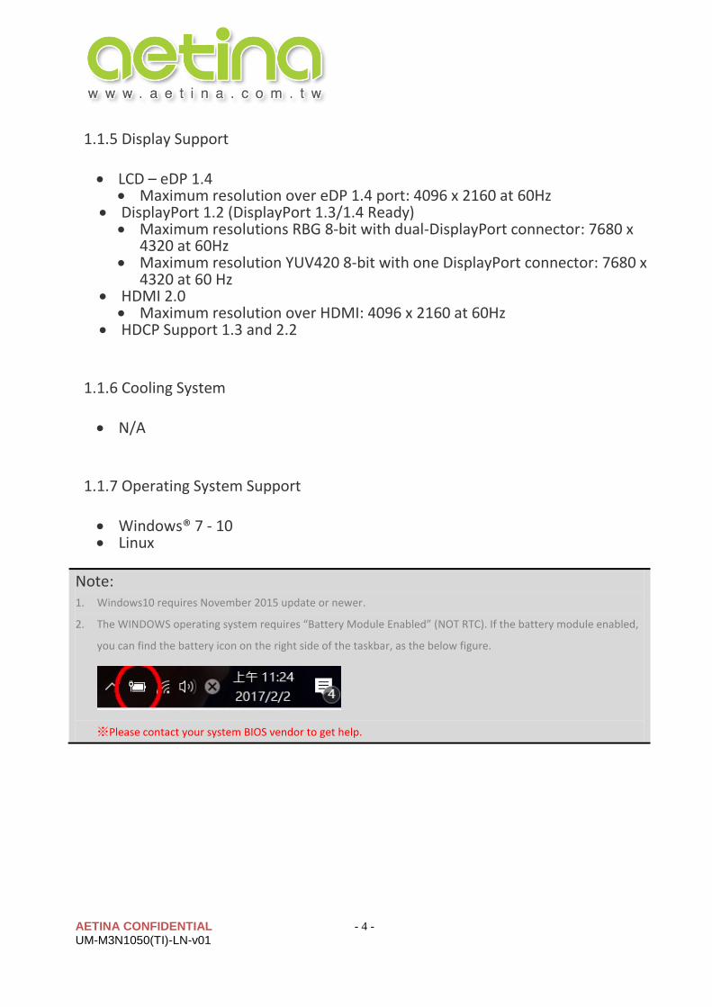
1.1.5 Display Support
LCD – eDP 1.4 Maximum resolution over eDP 1.4 port: 4096 x 2160 at 60Hz
DisplayPort 1.2 (DisplayPort 1.3/1.4 Ready) Maximum resolutions RBG 8-bit with dual-DisplayPort connector: 7680 x
4320 at 60Hz Maximum resolution YUV420 8-bit with one DisplayPort connector: 7680 x
4320 at 60 Hz HDMI 2.0
Maximum resolution over HDMI: 4096 x 2160 at 60Hz HDCP Support 1.3 and 2.2
1.1.6 Cooling System
N/A
1.1.7 Operating System Support
Windows® 7 - 10 Linux
Note: 1. Windows10 requires November 2015 update or newer.
2. The WINDOWS operating system requires “Battery Module Enabled” (NOT RTC). If the battery module enabled,
you can find the battery icon on the right side of the taskbar, as the below figure.
※Please contact your system BIOS vendor to get help.

AETINA CONFIDENTIAL UM-M3N1050(TI)-LN-v01
- 5 -
1.2 Configuration Table 1.1 lists the SKU configuration currently available for the GeForce GTX 1050(Ti) MXM graphics module.
Table 1.1: Board configuration
Specification M3N1050-LN Description M3N1050TI-LN Description
Chip GeForce GTX 1050 GeForce GTX 1050Ti
Core clock 1354MHz 1493MHz
Memory clock 3500MHz (7.0 Gbps) 3500MHz (7.0 Gbps)
Frame buffer 4 GB GDDR5 4 GB GDDR5
Memory interface 128-bit 128-bit
Memory type 256M x 32 GDDR5 FBGA-170
package
256M x 32 GDDR5 FBGA-170
package
Memory AVL Samsung K4G80325FB-HC28 Samsung K4G80325FB-HC28
Maximum board power 50 W 60 W
Connectors MXM 3.0 Connector
Interoperability
MXM 3.0 Connector
Interoperability
HDCP support Yes Yes
Supplementary Power
Connector
N/A N/A
Operating Temperature Standard: 0°C to +55°C
Extended Temp.: -20°C to +70°C
Wide Temp.: -40°C to +85°C
Standard: 0°C to +55°C
Extended Temp.: -20°C to +70°C
Wide Temp.: -40°C to +85°C
Storage Temperature -40°C to 125°C -40°C to 125°C
Operating Humidity 10~90%, No Condensation. 10~90%, No Condensation.

AETINA CONFIDENTIAL UM-M3N1050(TI)-LN-v01
- 6 -
2. Display Options
Table 2.1 list the GeForce GTX1050(Ti) MXM graphics module display options.
Table 2.1: Display Options
Displays Supported for Each Interface
DP_A DP_B DP_C DP_D DP_E DP_F
DisplayPort,
HDMI
DisplayPort
DisplayPort,
HDMI
eDP only DisplayPort,
DVI (single-link
or dual-link with
DP_F)
DisplayPort,
DVI (dual-link
with DP_E)
Note: 1. DP_P cannot be used for driving an external display.
2. System without Dual-link display can be supported up to four digital displays at the same time.
3. All display interfaces that support DisplayPort can be support dual-mode DisplayPort.

AETINA CONFIDENTIAL UM-M3N1050(TI)-LN-v01
- 7 -
3. Functional Description
3.1 Board Architecture
The AETINA M3N1050-LN & M3N1050TI-LN are based on MXM 3.1 Type A form
factor.
Figure 3.1: Block diagram
3.2 General Purpose Graphics Processing Unit
The AETINA GeForce GTX1050(Ti) MXM series are based on NVIDIA Pascal GPU. M3N1050-LN is based on GeForce GTX 1050. 640 CUDA core enabled and M3N1050TI-LN is based on GeForce GTX 1050Ti. 768 CUDA core enabled. All of them are compliant with NVIDIA’s CUDA compute capability 6.1.
3.2.1 Gpu Resoures
GeForce GTX 1050 GDDR5 SDRAM
-4 pieces 256M x 32 GDDR5, total capacity of 4096 Mbytes -128bit data bus width -7.0 Gbps clock frequency
BIOS ROM -4Mbit SPI FLASH for BIOS image

AETINA CONFIDENTIAL UM-M3N1050(TI)-LN-v01
- 8 -
GeForce GTX 1050Ti
GDDR5 SDRAM -4 pieces 256M x 32 GDDR5, total capacity of 4096 Mbytes -128bit data bus width -7.0 Gbps clock frequency
BIOS ROM -4Mbit SPI FLASH for BIOS image
3.3 Display Interface (Optional)
The AETINA GeForce GTX1050(Ti) MXM provides six digital output channels. Four channels can be active at same time.
3.3.1 Graphics Output channels
Figure 3.2: Output channels
3.3.2 Digital Output
The AETINA GeForce GTX1050(Ti) MXM supported 6x digital outputs via MXM connector.
DP_A/DP_B/DP_C/DP_D/DP_E/DP_F; dual-mode DisplayPort; maximum resolution over digital port: 7680 x 4320 at 60 Hz.

AETINA CONFIDENTIAL UM-M3N1050(TI)-LN-v01
- 9 -
3.3.3 Analog Output
The AETINA GeForce GTX1050(Ti) MXM not supports analog output.
3.3.4 AUX
The AETINA GeForce GTX1050(Ti) MXM supports AUX for DisplayPort monitor.
3.3.5 Hot Plug
The AETINA GeForce GTX1050(Ti) MXM supports Hot Plug detect for digital monitors. 3.4 PCI Express
The AETINA GeForce GTX1050(Ti) MXM supports a native x16 PCI Express Gen3/2/1 bus interface and also supports x8 lane widths.

AETINA CONFIDENTIAL UM-M3N1050(TI)-LN-v01
- 10 -
4. Pin Definition
4.1 Board Interface
Figure 4.1: M3N1050(TI)-LN Board layout
The table 4.1 shows the board layout and connector to familiarize users with M3N1050(TI)-LN MXM graphics module.
Table 4.1: Board layout and connectors
Specification Describe
G1 GeForce GTX 1050/1050Ti GPU
CN1 MXM connector
G1
CN1

AETINA CONFIDENTIAL UM-M3N1050(TI)-LN-v01
- 11 -
4.2 MXM Pin Assignments
4.2.1 MXM Connector
Figure 4.2: MXM connector (card TOP)
Figure 4.3: MXM connector (card BOTTOM)
4.2.2 MXM connector Pinout

AETINA CONFIDENTIAL UM-M3N1050(TI)-LN-v01
- 12 -
Table 4.2: MXM connector pinout

AETINA CONFIDENTIAL UM-M3N1050(TI)-LN-v01
- 13 -
Table 4.3: MXM connector pinout (continued)

AETINA CONFIDENTIAL UM-M3N1050(TI)-LN-v01
- 14 -
4.2.3 MXM OEM Pin Assignment
Table 4.4: MXM pin assignment
MXM OEM/GPIO1 Signal Name IO Type
OEM 4 GPU_EVENT# IN
OEM 5 GC6_FB_EN OUT
OEM 6 GPU_STEREO OUT
OEM 7 FRAMELOCK# IN
Note: 1. If OEM pin is not in use, keep it NC in the system board.
2. Keep the RESERVE pin as NC in the system board.

AETINA CONFIDENTIAL UM-M3N1050(TI)-LN-v01
- 15 -
5. Mechanical Specifications
5.1 Dimensions
The Actual dimensions of the M3N1050(TI)-LN are shown in below.
Figure 5.1: Dimensions of M3N1050(TI)-LN
AETINA CONFIDENTIAL UM-M3N1050(TI)-LN-v01
- 16 -
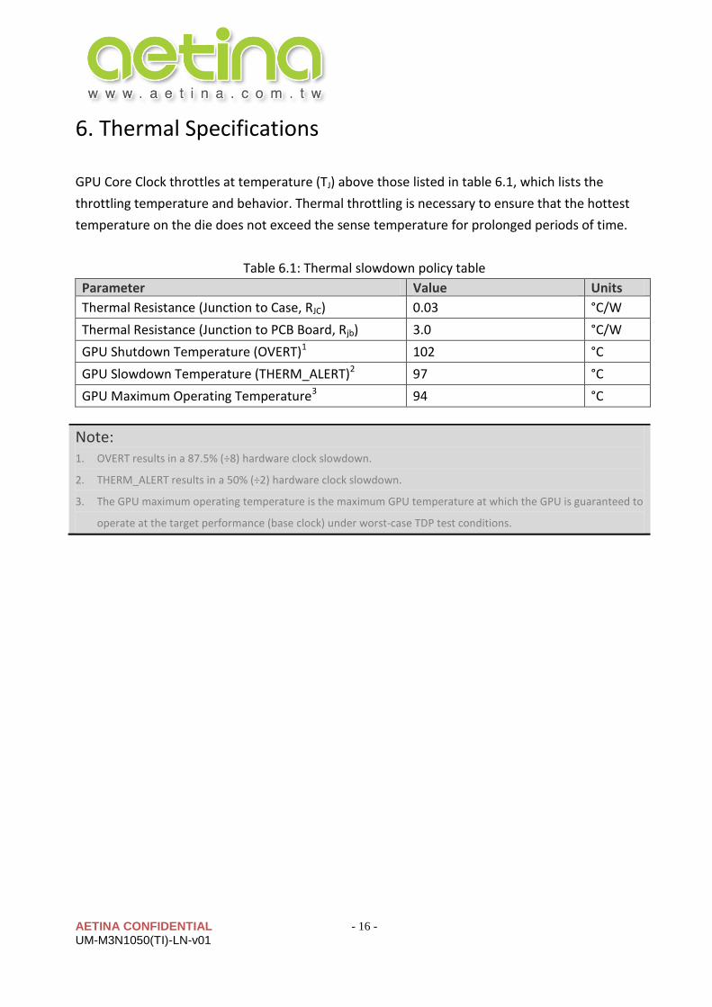
6. Thermal Specifications
GPU Core Clock throttles at temperature (TJ) above those listed in table 6.1, which lists the
throttling temperature and behavior. Thermal throttling is necessary to ensure that the hottest
temperature on the die does not exceed the sense temperature for prolonged periods of time.
Table 6.1: Thermal slowdown policy table
Parameter Value Units
Thermal Resistance (Junction to Case, RJC) 0.03 °C/W
Thermal Resistance (Junction to PCB Board, Rjb) 3.0 °C/W
GPU Shutdown Temperature (OVERT)1 102 °C
GPU Slowdown Temperature (THERM_ALERT)2 97 °C
GPU Maximum Operating Temperature3 94 °C
Note: 1. OVERT results in a 87.5% (÷8) hardware clock slowdown.
2. THERM_ALERT results in a 50% (÷2) hardware clock slowdown.
3. The GPU maximum operating temperature is the maximum GPU temperature at which the GPU is guaranteed to
operate at the target performance (base clock) under worst-case TDP test conditions.

AETINA CONFIDENTIAL UM-M3N1050(TI)-LN-v01
- 17 -
7. System Requirements
7.1 Power Sequencing
There is no power sequencing requirement for the input voltages to the MXM
module. However, the PWR_EN signal may be asserted only after all power rails are
within specified tolerance. The state of PWR_GOOD is undefined until all rails are
fully ramped.
Figure 7.1: Power sequencing No voltage shall be applied to any MXM module signal pin (except power pins and open drain signal specified in Table 7.1) until PWR_GOOD is asserted.
Table 7.1: Signals Exempted from Gating Requirement Group Signals
Power and Thermal SMB_CLK, SMB_DAT, TH_OVER#, TH_ALERT#, PWR_GOOD
System Management WAKE#, PEX_CLK_REQ# Display DP_x_HPD

AETINA CONFIDENTIAL UM-M3N1050(TI)-LN-v01
- 18 -
7.2 Module Power Down and Power Up
The MXM module may be powered down using the PWR_EN signal. The system designer may choose to shut down or keep the input power while the module is powered down.
Figure 7.2: Module power down All output signals from the MXM module are undefined when PWR_GOOD is deasserted or undefined. The system is recommended to gate critical signals using an appropriate qualifier. 7.3 Reset Requirements
System reset may be deasserted only after the assertion of the PWR_GOOD signal. Figure 7.3 shows the reset requirements relative to the PWR_EN and PWR_GOOD signals. This sequence must be followed on initial power on, system reset and resume from suspend/hibernate.
Figure 7.3: Reset Sequencing

AETINA CONFIDENTIAL UM-M3N1050(TI)-LN-v01
- 19 -
In order to reduce boot time, a system that monitors the PWR_GOOD signal, is allowed to violate the TPVPERL specification as long as the TPERST-PG timing is still met. 7.4 DisplayPort Interface
DC blocking capacitors of DisplayPort must be placed on the system board. In addition the MXM implementation of Dual-mode DisplayPort requires the circuit in Figure 5.4 on the AUX lines for proper dongle detection. The HPD signal conditioning must also be placed on the system board.
Figure 7.4: Dual-mode DisplayPort Implementation 7.5 Embedded DisplayPort (eDP)
Please contact Aetina for the eDP support. 7.6 DVI/HDMI on DP Interface
Native DVI or HDMI connector support can be implemented using a DisplayPort interface. Additional circuitry is required on the system and the proper signal mapping must be observed. As Figure 7.5 shows, 499Ω 1% pull-down resistors to ground on the DP lane signals must be placed on the connector side of AC coupling capacitors gated by a FET to limit the leakage. Additionally, level shifting circuits must also be implemented on DDC Data and Clock. Table 7.2 shows the mapping to connect the signals from the MXM connector to the HDMI/DVI connector. For the optional dual-link DVI support refer to Table 7.3.

AETINA CONFIDENTIAL UM-M3N1050(TI)-LN-v01
- 20 -
Table 7.2: DisplayPort Multiplexed signal definition
Pin Name DVI/HDMI DP_xL0
DP_xL0# TX_x_D2
TX_x_D2# DP_x_L1
DP_x_L1# TX_x_D1
TX_x_D1# DP_x_L2
DP_x_L2# TX_x_D0
TX_x_D0# DP_x_L3
DP_x_L3# TX_x_CLK
TX_x_CLK# DP_x_AUX DDC_x_CLK
DP_x_AUX# DDC_x_DAT
Figure 7.5: DVI/HDMI Implementation using DP Interface
Table 7.3: Dual-Link DVI Dual-Link DVI DP_A + DP_B DP_C + DP_D DP_E + DP_F
TX_CLK DP_A_L3 DP_C_L3 DP_E_L3 TX_D0 DP_A_L2 DP_C_L2 DP_E_L2 TX_D1 DP_A_L1 DP_C_L1 DP_E_L1 TX_D2 DP_A_L0 DP_C_L0 DP_E_L0 TX_D3 DP_B_L2 DP_D_L2 DP_F_L2 TX_D4 DP_B_L1 DP_D_L1 DP_F_L1 TX_D5 DP_B_L0 DP_D_L0 DP_F_L0 DDC DP_A_AUX DP_C_AUX DP_E_AUX
AETINA CONFIDENTIAL UM-M3N1050(TI)-LN-v01
- 21 -
7.7 Thermal and Power Management Interface
The thermal and power management interface of the MXM module consists of three main control signals in addition to SMBus interface used to read temperature and control various inputs to the temperature and power management interface. The three control signals can be described as system thermal and power protection (TH_OVERT#) and thermal and power system optimization (TH_ALERT# and TH_PWM). TH_OVERT# is a required open drain output from the MXM module which alerts the system that a critical temperature threshold has been crossed and the system must be shut down within 500 ms to prevent physical damage. The temperature threshold is defined as the minimum value of the module and the system limits. This feature is a fail-safe and should not occur during normal operation. TH_ALERT# is an optional open drain input/output of MXM module. On the MXM module side, the module will assert this signal to notify the system that its ALERT temperature has been crossed and it is taking steps to reduce the temperature and power of the module. On the system side, if the system determines the MXM module is operating in a temperature and power range it should not be, the system can assert the TH_ALERT# input to invoke the same temperature reduction mechanism to lower the temperature and power of the module. TH_PWM is an optional output of the MXM module which can be used to control a fan to optimize the MXM module performance and acoustic characteristics. The PWM frequency must be programmable between 10 and 30000Hz with duty cycle steps of no more than 1%.
Note: M3N1050(TI)-LN does not support TH_PWM function.
7.8 PWR_LEVEL Signal
The purpose of this pin is to give the system a hardware method for signaling the
module to reduce power consumption. The logic states are defined as 1 for full
power and 0 for reduced power. These two states may correspond to two power
levels defined in the MXM System Information Structure (input power substructure).
Refer to the MXM Graphics Module Software Specification for more information on
this substructure. Alternatively the module implementer may choose to associate
the pin states with other methods of power reduction. In any case the support of
this feature is required for the module and must provide at least 20% power
reduction from full power to reduced power. The use of this feature is optional for
the system (may be left unconnected).

AETINA CONFIDENTIAL UM-M3N1050(TI)-LN-v01
- 22 -
When PWR_LEVEL transitions from 1 to 0, the module must reduce power
consumption within 50 ms. In transitions from 0 to 1 the module may return to the
full power state within 250 ms.
The system should determine the values of the two power levels in the structure
based on the considerations of the maximum allowable current (10 A) through the
PWR_SRC rail limited by the capability of the MXM connector, and the maximum
allowable current of the battery. The system should drive PWR_LEVEL low whenever
a condition occurs that may cause the current through PWR_SRC to exceed 10 A, or
the total current drawn from the battery to exceed its limit. An example would be
that the AC adapter is inadvertently unplugged and the battery is running at a lower
voltage. In this case, the module, maintaining its higher power level, may draw a
current greater than 10A and damage the connector. Another example is a system
that contains more than one MXM module and operates at full power of each
module. When the AC adapter is unplugged in this case, the individual module may
not draw current more than 10A but the total current drawn from the battery may
exceed its limit. If the modules do not transition from high to low power in time, the
battery may be damaged.

AETINA CONFIDENTIAL UM-M3N1050(TI)-LN-v01
- 23 -
8. Certificates and Agencies
8.1 Certifications Please contact Aetina sales to get WHQL Driver for Windows 7 – 10.
8.2 Agencies Conformité Européenne (CE): TBD
Federal Communications Commission (FCC): TBD
AETINA CONFIDENTIAL UM-M3N1050(TI)-LN-v01
- 24 -
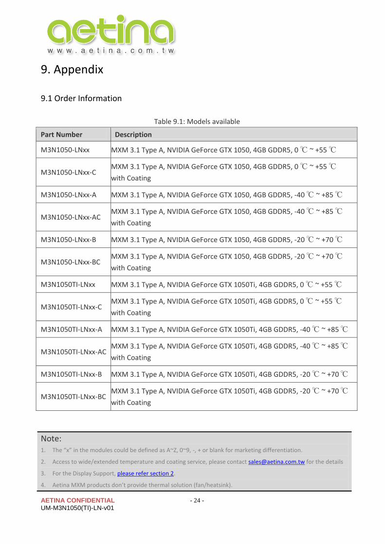
9. Appendix
9.1 Order Information
Table 9.1: Models available
Part Number Description
M3N1050-LNxx MXM 3.1 Type A, NVIDIA GeForce GTX 1050, 4GB GDDR5, 0 ~ +55
M3N1050-LNxx-C MXM 3.1 Type A, NVIDIA GeForce GTX 1050, 4GB GDDR5, 0 ~ +55
with Coating
M3N1050-LNxx-A MXM 3.1 Type A, NVIDIA GeForce GTX 1050, 4GB GDDR5, -40 ~ +85
M3N1050-LNxx-AC MXM 3.1 Type A, NVIDIA GeForce GTX 1050, 4GB GDDR5, -40 ~ +85
with Coating
M3N1050-LNxx-B MXM 3.1 Type A, NVIDIA GeForce GTX 1050, 4GB GDDR5, -20 ~ +70
M3N1050-LNxx-BC MXM 3.1 Type A, NVIDIA GeForce GTX 1050, 4GB GDDR5, -20 ~ +70
with Coating
M3N1050TI-LNxx MXM 3.1 Type A, NVIDIA GeForce GTX 1050Ti, 4GB GDDR5, 0 ~ +55
M3N1050TI-LNxx-C MXM 3.1 Type A, NVIDIA GeForce GTX 1050Ti, 4GB GDDR5, 0 ~ +55
with Coating
M3N1050TI-LNxx-A MXM 3.1 Type A, NVIDIA GeForce GTX 1050Ti, 4GB GDDR5, -40 ~ +85
M3N1050TI-LNxx-AC MXM 3.1 Type A, NVIDIA GeForce GTX 1050Ti, 4GB GDDR5, -40 ~ +85
with Coating
M3N1050TI-LNxx-B MXM 3.1 Type A, NVIDIA GeForce GTX 1050Ti, 4GB GDDR5, -20 ~ +70
M3N1050TI-LNxx-BC MXM 3.1 Type A, NVIDIA GeForce GTX 1050Ti, 4GB GDDR5, -20 ~ +70
with Coating
Note: 1. The “x” in the modules could be defined as A~Z, 0~9, -, + or blank for marketing differentiation.
2. Access to wide/extended temperature and coating service, please contact [email protected] for the details
3. For the Display Support, please refer section 2.
4. Aetina MXM products don’t provide thermal solution (fan/heatsink).
AETINA CONFIDENTIAL UM-M3N1050(TI)-LN-v01
- 1 -
Disclaimer
The information presented in this document is for informational purposes only and may contain technical inaccuracies, omissions and
typographical errors.
The information contained herein is subject to change and may be rendered inaccurate for many reasons, including but not limited to product
and roadmap changes, component and motherboard version changes, new model and/or product releases, product differences between differing
manufacturers, software changes, BIOS flashes, firmware upgrades, or the like. Aetina assumes no obligation to update or otherwise correct or
revise this information. However, Aetina reserves the right to revise this information and to make changes from time to time to the content hereof
without obligation of Aetina to notify any person of such revisions or changes.
Aetina MAKES NO REPRESENTATIONS OR WARRANTIES WITH RESPECT TO THE CONTENTS HEREOF AND ASSUMES NO RESPONSIBILITY FOR ANY
INACCURACIES, ERRORS OR OMISSIONS THAT MAY APPEAR IN THIS INFORMATION.
Aetina SPECIFICALLY DISCLAIMS ANY IMPLIED WARRANTIES OF MERCHANTABILITY OR FITNESS FOR ANY PARTICULAR PURPOSE. IN NO EVENT
WILL Aetina BE LIABLE TO ANY PERSON FOR ANY DIRECT, INDIRECT, SPECIAL OR OTHER CONSEQUENTIAL DAMAGES ARISING FROM THE USE OF ANY
INFORMATION CONTAINED HEREIN, EVEN IF NVIDIA IS EXPRESSLY ADVISED OF THE POSSIBILITY OF SUCH DAMAGES.