using process step verification (psv) to ensure … · using process step verification (psv) to...
TRANSCRIPT

Jeffrey Quinton F.B. Lynch - Slide 1
Using Process Step Verification (PSV) to Ensure Wafers Have Completed All
Process Steps
Jeffrey Quinton of Delphi Electronics & SafetyF.B. Lynch, III of Electroglas, Inc.

Jeffrey Quinton F.B. Lynch - Slide 2
Presentation• Who is Delphi• PSV Abstract• Processing Without PSV• Examples of Process Violations• Cost of a Process Violation• How Does PSV WORK• Other Considerations for
Implementation of PSV• Conclusions

Jeffrey Quinton F.B. Lynch - Slide 3
Who Is Delphi?• Delphi is a world leader in mobile electronics and
transportation components and systems technology
• Multi-national Delphi– Conducts its business operations through various subsidiaries
and has headquarters in Troy, Mich., USA, Paris, Tokyo and São Paulo, Brazil.
• Delphi's two business sectors – Dynamics, Propulsion, Thermal, and Interior Sector– Electrical, Electronics, and Safety Sector
• Delphi has approximately 185,000 employees and operates 171 wholly owned manufacturing sites, 42 joint ventures, 53 customer centers and sales offices and 33 technical centers in 40 countries.

Jeffrey Quinton F.B. Lynch - Slide 4
Delphi
Serving DiverseCustomers and Markets
Automotive Medical Truck Bus Marine

Jeffrey Quinton F.B. Lynch - Slide 5
Delphi Electronics & SafetyGlobal Presence
27,381
36
Manufacturing Sites:Employment:
Customer Centers:Technical Centers:
United States
515,677
35
Manufacturing Sites:Employment:
Customer Centers:Technical Centers:
Mexico & South America
84,432
1012
Manufacturing Sites:Employment:
Customer Centers:Technical Centers:
Europe
32,921
57
Manufacturing Sites:Employment:
Customer Centers:Technical Centers:
Asia/Pacific
1dd05-19.0*Regional breakdown is consistent message throughout Delphi.

Jeffrey Quinton F.B. Lynch - Slide 6
Delphi Electronics & Safety
Breadth of ProductBody
Powertrain
Safety
Integrated Media Systems
1dd05-16.0
Security Systems• Vehicle• Content
Body ElectronicsClimate ControllersHead-up DisplaysInstrument Clusters
Standalone & Engine Management System Controllers
• Engine• Machine and Heavy Duty• Powertrain• Transmission
Power ModulesSemiconductorsSoftware
Airbags•Frontal, Side, Curtain•Inflators, Cushions, Covers
Antilock Brake ControlBelt Tension SensorSeat BeltsSteering WheelsSuspension Electronic Control
Forewarn® Collision Warning Systems• Smart Cruise Control• Back-up Aid• Side Alert
Restraint Systems Electronics• Crash Sensing• Occupant Sensing
Steering Electronic Control
Acoustic SystemsAdvanced Digital Audio
• Playback Devices • Satellite Receivers• Digital Receivers
AmplifiersFuba® Advanced Antenna Systems
Hands-free Connectivity Navigation SystemsPremium Audio SystemsRear Seat Entertainment SystemsReceiversSatellite Data Services and CommunicationTruck PCWireless Networking
Jeffrey Quinton F.B. Lynch - Slide 7
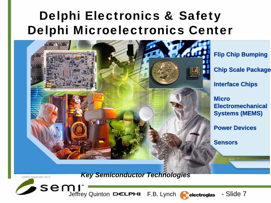
Delphi Electronics & Safety Delphi Microelectronics Center
1dd05-Appendix 45.0 Key Semiconductor Technologies
Flip Chip Bumping
Chip Scale Package
Interface Chips
Micro ElectromechanicalSystems (MEMS)
Power Devices
Sensors
Flip Chip Bumping
Chip Scale Package
Interface Chips
Micro ElectromechanicalSystems (MEMS)
Power Devices
Sensors

Jeffrey Quinton F.B. Lynch - Slide 8
Delphi Electronics & Safety
Harnessing the Power of MicroelectronicsFrom the Miniature World of Microelectronics, We Generate “Big Solutions” for Our Customers– Progressing Beyond the Concept of Up-
integration to Creating “Systems on a Chip”– Creating Platforms Geared to Specific
Applications and Markets– Reusing High-quality, Reliable Building Blocks
and Modules Selectively to Reduce Product Size, Cost and Complexity
Results in Cost-effective “Toolkits” for Multiple Market Applications
1dd05-32.0

Jeffrey Quinton F.B. Lynch - Slide 9
Dept 8436 - Wafer Test, Saw and Sort• 150 Products
– CMOS, Bipolar, Smart Power, IGBT, Micro Machine, and Sensors
– Flip Chip and Pad Devices
• 87 Test Cells– Teradyne A5xx, A3xx, J9xx - Sentry - SZ M3020 - LTX 77,
CP80, Synchro HT, CX– EG2001, EG2010, EG4090 and TEL P8XL, WDF Probers– Offline Ink
• Test 1,000,000 Die Per Day– 3 Shifts, 5 Days/week Operation
• Automatic Visual Inspect, Saw, and Sort• Packaging and Final Test

Jeffrey Quinton F.B. Lynch - Slide 10
PSV Abstract
• Process Step Verification (PSV)… provides a method to assure that wafers / lots will accurately flow through a pre-defined set of process steps.
• Wafers / Lots at any step in a process will not be tested or processed until they have completed all previous steps in the process.
• The system has been designed to be flexible such that it can be adapted to accommodate virtually any process, and can be integrated with equipment from third party vendors.

Jeffrey Quinton F.B. Lynch - Slide 11
Processing Without PSV• No problem with wafers that are
tested once, inked and sorted.• Multi-Pass Devices are at Risk
– Wafers that are tested, sent to bump room and come back for second pass test.
– Wafers that go through 3-4 test passes.– Wafers that go through automatic visual
inspection process.

Jeffrey Quinton F.B. Lynch - Slide 12
FabInspection
Pass 1Test
Pass 2Test
Pass 3Test
Pass 4Test
OfflineInk
AutomaticWafer
Inspection
DiePackage
Die Sort
OutsideCustomer
DELPHI PROCESS FLOW
Jeffrey Quinton F.B. Lynch - Slide 13
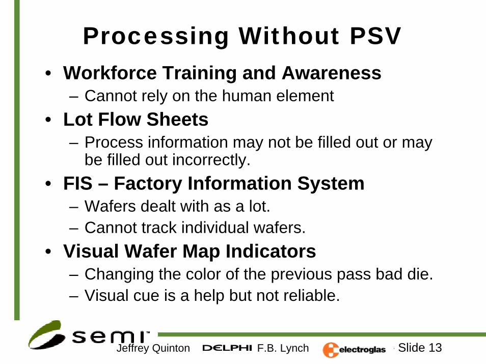
Processing Without PSV• Workforce Training and Awareness
– Cannot rely on the human element• Lot Flow Sheets
– Process information may not be filled out or may be filled out incorrectly.
• FIS – Factory Information System– Wafers dealt with as a lot.– Cannot track individual wafers.
• Visual Wafer Map Indicators– Changing the color of the previous pass bad die.– Visual cue is a help but not reliable.

Jeffrey Quinton F.B. Lynch - Slide 14
Processing Without PSV• Automatic Visual Inspection
– Adds additional ink dots to identify visually defective die.
– You cannot look at a wafer and know it has been inspected.
• Die Sort– New Lot Flow Sheet – cannot look at previous
processes.– Sort by ink dot or whatever map is available.– Machine cannot tell which map it is using.
• Offsite Wafer Processing (Packaging)– No indication of what process steps the wafer has
completed. – Correct wafer map must be provided.

Jeffrey Quinton F.B. Lynch - Slide 15
Examples of Process Violations• Example One: Device ABCD is a flip chip
IC used in a safety critical application in the vehicle. – First pass functional test.
• The last step of first pass test is to program some memory cells.
– 24 hour retention bake and Second pass test. • Second pass test is to make sure the memory cells
retain programming. – UV erase and a Third pass test
• Ensure devices were erased properly. – Automatic visual inspection to check for
mechanical or bump damage.

Jeffrey Quinton F.B. Lynch - Slide 16
Examples of Process Violations
• Result of a Missed Process Step – A module level failure at final assembly
• lost dollars due to scrap and replacement. – Latent failure after the module is placed in
a vehicle. • Warranty return with associated cost• Loss of customer confidence

Jeffrey Quinton F.B. Lynch - Slide 17
Examples of Process ViolationsExample Two: Device XYZ is a flip chip used in an automotive application.
• Functional test before bump process.– No inking is done to the device after this step. – Wafer map is the only evidence wafer was tested.
• Bump process – The part may not come back to test for several days.
• Second pass test follows the first pass map– Second pass is not a full functional test.
• Automatic visual inspect and die sort. • Module assembly
– Full functionality of the specific IC cannot be tested due to it being a part of a circuit.

Jeffrey Quinton F.B. Lynch - Slide 18
Examples of Process Violations
• Result of a Missed Process Step – Same cost as example 1
• Additional cost– Investment of engineering hours spent trying to
salvage the material:• Risk Assessment
– How many bad die did the customer receive?– What impact would there be on module functionality?
• Typically, there will only be a few bad die in the reel.– In one instance there were 17 bad modules in a lot of
8000 modules. – Is there some way to sort out the 17 and ship the rest or
do we have to scrap all 8000 units?

Jeffrey Quinton F.B. Lynch - Slide 19
Cost of a Process Violation
25 X $1000 = $25,000 Wafer Cost4 hours X $250 = $ 1,000 Engineering TimeReplacement Cost = $25,000 Product Replacement OT/Premium Ship = $ 9,000 Additional CostTotal Material/Labor Cost = $60,000Total Cost = ?? (Loss of Customer Confidence)
• Customer loss is difficult to compute due to unknown impact on customer confidence and impacts to their scheduling and downstream end users / customers.
• Supplier has seven (7) process violations per year. • Annual loss = 7 X $60,000 = $420,000

Jeffrey Quinton F.B. Lynch - Slide 20
How Does PSV Work
• Process result maps are generated at the first test or visual inspection step.
• All subsequent process steps utilize / follow this result map processing only good die.
• If a process step is missed the subsequent process step will not follow or process a wafer map that does not have the correct information.

Jeffrey Quinton F.B. Lynch - Slide 21
Process Step Verification Integration

Jeffrey Quinton F.B. Lynch - Slide 22
Process Monitoring Solutions
• Traditional Solutions– Weaknesses
• Lot based verification
• Process Step Verification– Advantages
• Integrates to MES• Lot, Wafer and
individual Die based verification
• Alarms / Messages to equipment / process owners of process violations

Jeffrey Quinton F.B. Lynch - Slide 23
How Does PSV Work
• PSV involves putting flag(s) in the wafer map file which tracks process step(s) the wafer has been through.
• The wafer mapping system has a database / wafer map repository that monitors and validates all process steps for each product type.

Jeffrey Quinton F.B. Lynch - Slide 24
How PSV Works - PSV Flow• Wafer Begins the Test Process at Pass 1
– A wafer map containing X/Y coordinate and bin information is created and stored in the map repository with unique Wafer ID.
– The lot header information includes the prior process step flag which is unique to the device and process.
• Wafer is Ready for the Next Step in the process, Pass 2– A dummy (0 bin) wafer map is sent to the wafer map repository.
• This map contains a prior process step flag specific to the process flow and process step of this device.
– The wafer map repository checks to see if a map is available with the previous process step flag and if it is the correct process step in the process flow. • If everything is ok a map is sent to the machine and
processing continues• If everything is not ok a message is sent to the operator,
telling them to check the wafer for correct processing.• PSV Continues for all Process Steps for the Device
Jeffrey Quinton F.B. Lynch - Slide 25
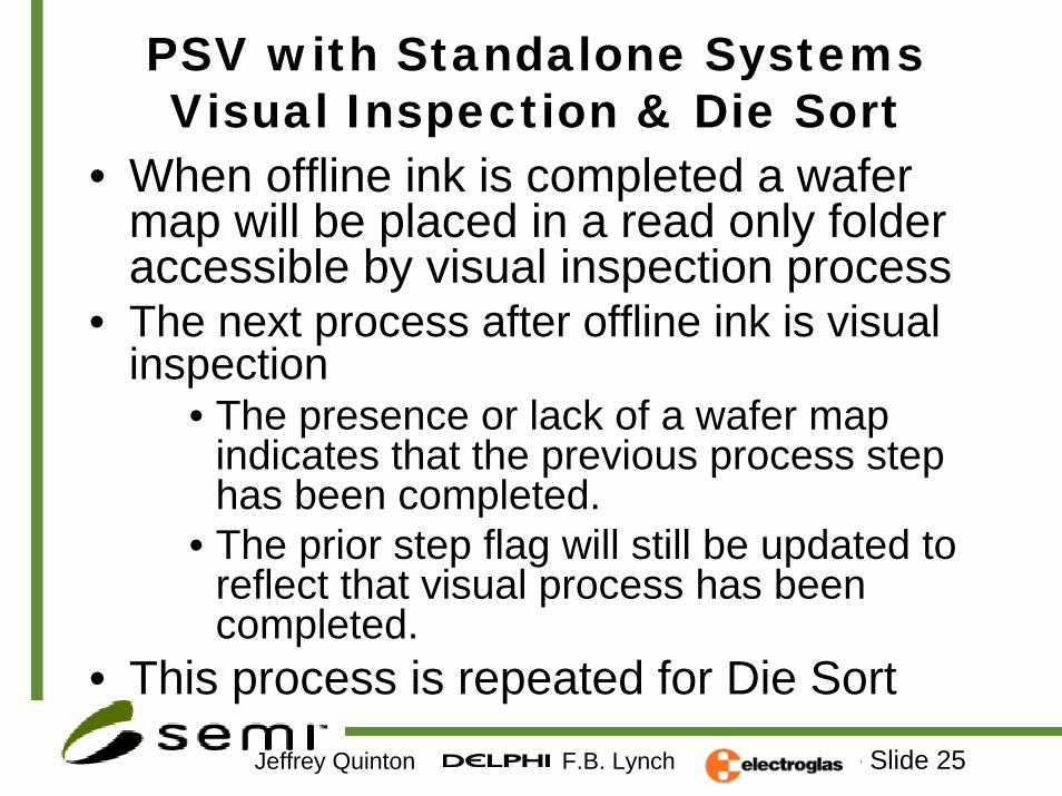
PSV with Standalone SystemsVisual Inspection & Die Sort
• When offline ink is completed a wafer map will be placed in a read only folder accessible by visual inspection process
• The next process after offline ink is visual inspection
• The presence or lack of a wafer map indicates that the previous process step has been completed.
• The prior step flag will still be updated to reflect that visual process has been completed.
• This process is repeated for Die Sort

Jeffrey Quinton F.B. Lynch - Slide 26
MAPRepository
SORTmanager
4090 Prober4090 Prober
4090 Prober4090 Prober
4090 Prober
AugustInspectionAugust
InspectionAugustInspectionAugust
Inspection
DmatixDie SorterDmatix
Die SorterDmatixDie SorterDmatix
Die SorterDymatixDie Sorter
Fab Visual
Dept 869Packaging
OffshorePackaging
DelphiSingapore
FISProcess Control
Incoming
ScribeReader
OutgoingScribe Reader
Lot and WaferTracking. Lot Verification.
TEL ProberTEL Prober
TEL Prober
TEL Prober
Camtek
Factory
Information
System
Wafer MapsPrior StepVerification
Future Integration Projects

Jeffrey Quinton F.B. Lynch - Slide 27
Other Considerations for Implementation of PSV
• First Die Integrity at Every Process Step– If first die is not correct, PSV will be of no value.
• Computer Hardware and Networking Infrastructure Must be 99.9 +% Dependable – If one goes back to a manual process they can no longer
guarantee a device has seen all of the process steps and that the resultant IC is a KGD.
• Standard Wafer Map Format – Format that can be specified to any equipment vendor.– Compatibility with equipment used by offshore assembly
houses. • Robust Wafer Laser Scribe Process
– Laser scribe integrity becomes the most important step in the Fab process.

Jeffrey Quinton F.B. Lynch - Slide 28
Conclusion• Customer Expectations
– Known Good Die• An unpackaged IC chip which will meet or exceed the
electrical specifications and reliability established for the packaged part.
• Meet or exceed the requirements of the intended hybrid or MCM (Multi-Chip Module) application.– Die cost 60 cents : Module cost $100.00– Full IC functionality (hot/room/cold) cannot be tested at
module level test.
– Customers expect 0 PPM

Jeffrey Quinton F.B. Lynch - Slide 29
Conclusions• Effective process management requires the ability to
take corrective action quickly when an out-of control process condition occurs.
• Prompt corrective action requires obtaining and managing data from a variety of sources and presenting those data in a manner that facilitates quick decision-making.
• Since every manufacturing environment is different, any solution must support extensible and unique customization.
• Users tend to be widely dispersed geographically–from corporate headquarters to remote locations, customer sites, and supplier facilities – collaboration requires a solution with both local and remote access via the Internet.
• PSV is that solution at Delphi.

Jeffrey Quinton F.B. Lynch - Slide 30
Conclusions• PSV Results
– Since the implementation of Process Step Verification at Delphi we have not had a missed process step or experienced any quality spills to any of our customers.
– Delphi ROI (return on investment) for (PSV) was 0.5 years (6 months) based on investment, throughput optimization and scrap savings.