using the flexible ‘5xx universal clock system … 5/22/2008 1 using the flexible ‘5xx universal...
TRANSCRIPT

1
5/22/2008 1
Using the flexible ‘5xx Universal Clock System (UCS)Stefan Schauer
2
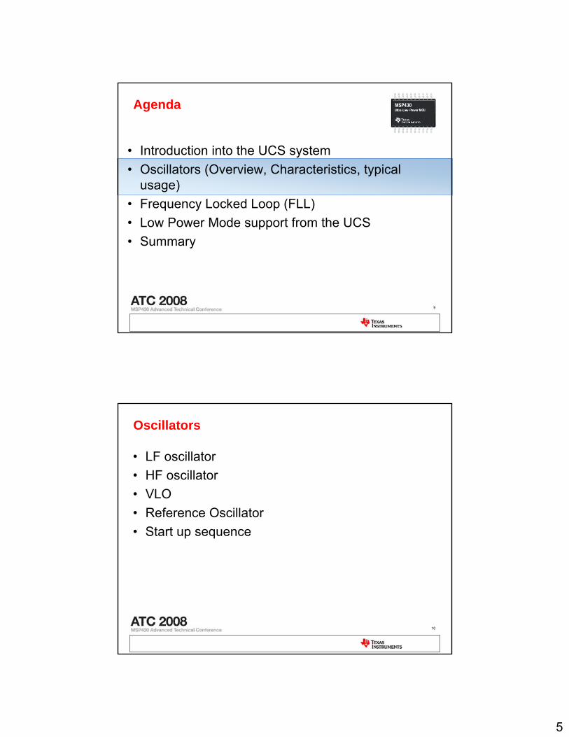
Agenda
• Introduction into the UCS system• Oscillators (Overview, Characteristics, typical
usage)• Frequency Locked Loop (FLL)• Low Power Mode support from the UCS• Summary

2
3
• Three low-freq sources– LFXT1– VLO– REFO
• FLL reference selectable from LFXT1, REFO, or XT2
• ACLK/SMCLK/MCLK can all be driven from any source
• MODOSC provided to modules– Example: Flash controller and
ADC
• PLL for USB devices only– Up-converts 4-24MHz XT1/2 to
internal 48MHz for USB communication
F5xx Unified Clock System (UCS)
Divider/1/2/4/8/16
10-bitFrequency Integrator
FLL
DCO
FLLREFCLK
DCOCLK
DCOCLKDIV
VLO
REFO
LFXT1
XT2
ACLK
MCLK
SMCLK
MODOSCMODCLK
Provided to Flash controller, ADC12
4
UCS Comparison to 4xx and 1xx
• Using best of FLL and Basic Clock– FLL– High clock flexibility
• Existing clocks essentially unchanged – XT1/XT2/DCO/FLL
• Increased clock orthogonality– Any source can drive any system
clock• Crystal pins muxed with I/O
function, defaulting as I/O– Must be initialized to crystal
function• Clock divider on all clock tree
outputs

3
5
Low Frequency Clock Sources
Range of choices to fit application needs
ZEROLOW<500nAVLO
ZEROMEDIUM3uAREFO
COMPONENTHIGH1uAXTAL
COSTPRECISIONPOWER
(Current included in Active and LPM0-3 current if clock is used for ACLK)
6
High Frequency Clock Sources
Range of choices to fit application needs
ZERODepends on Ref + Jitter60uA @ 1MHzDCO
COMPONENTHIGH60uA @ 12MHz150uA @ 20MHz300uA @ 32MHz
XTAL (XT2)
COMPONENTHIGH60uA @ 12MHz150uA @ 20MHz300uA @ 32MHz
XTAL (XT1)
COSTPRECISIONPOWER
(DCO Current included in Active and LPM0 current)

4
7
5xx FLL Overview
• FLL: Adjust DCO frequency in reference to a lower clock source (similar to PLL)
• Normally the FLL is used as source for the MCLK (CPU)
• Very flexible scaling of the output frequency
• Sources for Reference: REFO / LFXT1/XT1 / XT2
• Output frequency: 100kHz - >32Mhz
8
Frequency Locked Loop (FLL) functionality
• The System Clock of controllers has to meet different requirements, according to the application and system conditions:– High frequency, to react fast onto system hardware requests or events– Low frequency, to minimize current consumption, EMI, .....– Stable frequency for timer applications e.g. real time clock RTC– Low-Q oscillators to enable start-stop operation with 'zero' delay to
operation.• All these conflicting but essential requests can not be handled, with
– high-Q, fast frequency crystals– low-Q RC-type oscillators
• Lowest current consumption and frequency stability require the use of a low frequency crystal.
• The compromise used in the MSP430 is to use a low frequency crystal, and to multiply its frequency up to the nominal operating range.
5
9
Agenda
• Introduction into the UCS system• Oscillators (Overview, Characteristics, typical
usage)• Frequency Locked Loop (FLL)• Low Power Mode support from the UCS• Summary
10
Oscillators
• LF oscillator• HF oscillator• VLO• Reference Oscillator• Start up sequence

6
11
LF oscillator
• Support for 32kHz Crystal• Startup time < 1000ms• Internal Load Caps for Crystal:
2pF, 5.5pF, 8.5pF, 12pF (effective)• Adjustment of drive strength (0- 3)
– Default: highest setting for highest safety factor• Oscillator Allowance:
– 210 kOhm at 6pF (Drive Strength: 0 / Safety Factor: 5)– 300 kOhm at 12pF (Drive Strength: 1 / Safety Factor: 5)
• Separate fault flag for LFXT Oscillator• Many improvement for stability have been added
compared to older families• Bypass mode to feed in external digital clock
12
HF oscillator
• Support for 4 -32 MHz Crystal• Startup time < 10ms (6MHz Crystal)• Oscillator Allowance: 450 Ohm at 6MHz
320 Ohm at 12MHz200 Ohm at 20MHz200 Ohm at 32MHz
• No internal Load Caps for Crystal:(add 1pF from Bond Pads)
• Adjustment of drive strength (default highest setting)• Bypass mode to feed in external clock• XT1 and XT2 identical
7
13
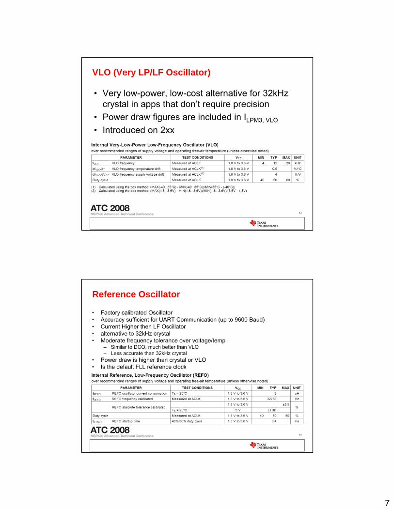
VLO (Very LP/LF Oscillator)
• Very low-power, low-cost alternative for 32kHz crystal in apps that don’t require precision
• Power draw figures are included in ILPM3, VLO
• Introduced on 2xx
14
Reference Oscillator
• Factory calibrated Oscillator• Accuracy sufficient for UART Communication (up to 9600 Baud)• Current Higher then LF Oscillator• alternative to 32kHz crystal• Moderate frequency tolerance over voltage/temp
– Similar to DCO, much better than VLO– Less accurate than 32kHz crystal
• Power draw is higher than crystal or VLO• Is the default FLL reference clock

8
15
What Can You Do With REFO?
• Periodic wakeup for apps in which these are true…– Don’t need crystal accuracy…– But need better accuracy than VLO– More cost-sensitive than power-sensitive
• Can you do RTC?– Not really -- +/-2% error means ~ +/- 1/2 hour error
every day– But not bad as a ‘walking wounded’ RTC mode in event
of crystal failure!
16
MODOSC
• Internal oscillator to help automate operation of some modules– Substitute for source clock in Flash module
No configuration of fFTG requiredNo Risk of bad programming due to wrong Flash clock
– Serves as ADC12_A’s internal oscillator (ADC12OSC)
• ~ 5MHz• Not available to system clocks – direct to modules• Generally for applications in which drift isn’t critical• Activation on demand
– Flash activates it automatically when programming or erasing– ADC12 activates it when chosen as conversion clock

9
17
RQRLLQ
-RINV CL
Condition for oscillation:|-RINV| = RL + RQmax
Safety Factor:
SF = RQmax
RLmax
Safety Factor Qualification
SF < 1.5 unsuitable1.5 ≤ SF < 2 risky2 ≤ SF < 3 suitable3 ≤ SF < 5 safeSF ≥ 5 very safe
Oscillator Allowance
• Load Capacitance CL contains C1, C2 and CS
• The amplification capability of the oscillator inverter is replaced with a negative resistance –RINV
• The quartz crystal is replaced by the load resonance resistance RL (effective resistance) and the effective Reactance LQ.
18
Crystal Layout
• Crystal as close the to MSP430 as possible• Short and direct traces, no traces underneath• Keep away switching signals• Ground crystal can, use guard ring around leads• Ground plane underneath crystal
10
19
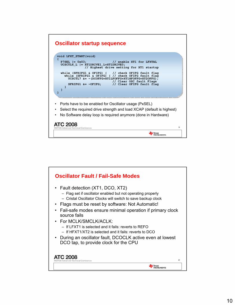
Oscillator startup sequence
• Ports have to be enabled for Oscillator usage (PxSEL)• Select the required drive strength and load XCAP (default is highest)• No Software delay loop is required anymore (done in Hardware)
void LFXT_START(void){
P7SEL |= 0x03; // enable XT1 for LFXTALUCSCTL6_L |= XT1DRIVE1_L+XT1DRIVE0;
// Highest drive setting for XT1 startup
while (SFRIFG1 & OFIFG) { // check OFIFG fault flagwhile (SFRIFG1 & OFIFG) { // check OFIFG fault flag
UCSCTL7 &= ~(DCOFFG+XT1LFOFFG+XT1HFOFFG+XT2OFFG); // Clear OSC fault Flags
SFRIFG1 &= ~OFIFG; // Clear OFIFG fault flag}
}}
20
Oscillator Fault / Fail-Safe Modes
• Fault detection (XT1, DCO, XT2)– Flag set if oscillator enabled but not operating properly – Cristal Oscillator Clocks will switch to save backup clock
• Flags must be reset by software: Not Automatic!• Fail-safe modes ensure minimal operation if primary clock
source fails• For MCLK/SMCLK/ACLK:
– If LFXT1 is selected and it fails: reverts to REFO– If HFXT1/XT2 is selected and it fails: reverts to DCO
• During an oscillator fault, DCOCLK active even at lowest DCO tap, to provide clock for the CPU

11
21
Oscillator Fail-Safes vs 2xx/4xx
• Similar to 2xx/4xx, except….• If LF crystal fails, REFO now takes over
– In 2xx/4xx, DCO takes over (only for WDT+)– Robust, but large freq difference can affect operation
• REFO and crystal have same nominal frequency, allowing similar functionality
• Remember:– REFO tolerance isn’t as tight – not a replacement for
crystal in all cases– Current draw is higher than crystal -- 3uA (typ)
22
Oscillator failsafe - Backup clocks
Original Source: LFXT1
Original Source: Other
Divider/1/2/4/8/16
10-bitFrequency Integrator
FLL
DCO
FLLREFCLK
DCOCLK
DCOCLKDIV
VLO
REFO
LFXT1
XT2
ACLK
MCLK
SMCLK
MODOSCMODCLK
Provided to Flash controller, ADC12
Off
12
23
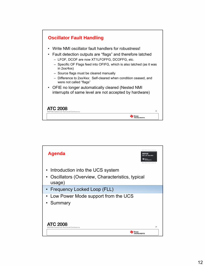
Oscillator Fault Handling
• Write NMI oscillator fault handlers for robustness!• Fault detection outputs are “flags” and therefore latched
– LFOF, DCOF are now XT1LFOFFG, DCOFFG, etc.– Specific OF Flags feed into OFIFG, which is also latched (as it was
in 2xx/4xx)– Source flags must be cleared manually– Difference to 2xx/4xx: Self-cleared when condition ceased, and
were not called “flags”
• OFIE no longer automatically cleared (Nested NMI interrupts of same level are not accepted by hardware)
24
Agenda
• Introduction into the UCS system• Oscillators (Overview, Characteristics, typical
usage)• Frequency Locked Loop (FLL)• Low Power Mode support from the UCS• Summary
13
25
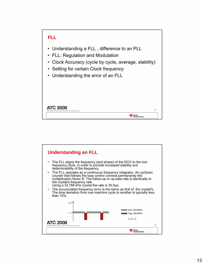
FLL
• Understanding a FLL , difference to an PLL• FLL: Regulation and Modulation• Clock Accuracy (cycle by cycle, average, stability)• Setting for certain Clock frequency• Understanding the error of an FLL
26
Understanding an FLL
• The FLL aligns the frequency (and phase) of the DCO to the low-frequency clock, in order to provide increased stability and determinability of the frequency.
• The FLL operates as a continuous frequency integrator. An up/down counter that follows the loop control corrects permanently the multiplication factor N. The follow-up or up-date rate is identically to the crystal's frequency rate. Using a 32,768 kHz crystal the rate is 30.5µs.
• The accumulated frequency error is the same as that of the crystal's. The time deviation from one machine cycle to another is typically less than 10%.
Δ f
pos. deviationneg. deviation
Σ Δf = 0

14
27
Digital Controlled Oscillator
• The operating range is controlled by: – DCORSEL0…DCORSEL2– Wide Range Area
• Digital Controlled Oscillator is controlled by– DCO0…DCO5– Frequency Tap for fine adjustment
• Five modulation bits MOD0 to MOD4 to define the timing interval
5DCO
Modulator
+1
DCO
5MOD
SCG1
DCOCLK
DISMODDCORSEL
0 1 2
reference clock e.g. ACLKSW or FLL controls the DCOCLK
DC -Generator
to clock distribution network
28
Note: The SCG0 bit in the Status Register (SR) controls the FLL loop (open or closed).Note: The SCG0 bit in the Status Register (SR) controls the FLL loop (open or closed).
FLL: Blockdiagram

15
29
29
FLL: Digital Oscillator Loop Control
• D: FLL Loop Divider in UCSCTL2 (FLLD bits)• N: Multiplier Bits in UCSCTL2 (FLLN bits)
(must be greater then 0)• n: DCO tap selection in UCSCTL 0
(Modified automatically by the FLL)
f(DCOCLK) = D x ( N + 1 ) × f(FLLRefClock) / n
The content of N defines the system frequency if the FLL is active.The content of N defines the system frequency if the FLL is active.
30
FLL: Selection of Nominal Frequency

16
31
Frequency Cycle time
selected:f3:f4:
1000 kHz 1000 nsec
943 kHz 1060 nsec
1042 kHz 960 nsec
Selected Selected frequencyfrequency
f2 f3 f4 f5 f6
DCOCLK
DCO +0+1
t periodΣError of
Modulation Period
+20+40
-40-20
0
[nsec]
t periodΣError of
[%]+4+3+2+1
0-1-2-3-4
MOD = 19
FLL: Modulation
32
FLL: Regulation and Modulation
• On each Ref Clock Cycle the DCO tap and the modulation is updated
• The DCO could get one tap up or down.• If the Frequency is locked the Tap will stay almost
the same and only the Modulation is changed.• The Modulation allows to change the DCO with
each DCO clock cycle to the adjusted frequency and the frequency of the Tap +1 to get less time for zero frequency error.

17
33
Understanding the Error of an FLL
FLL Error
-0.01
0
0.01
0.02
0.03
0.04
0.05
0.06
0.07
1 6 11 16 21 26 31 36 41 46 51 56 61 66 71 76 81 86 91
Clock Cycles
Erro
r [%
]
Error
• Clock Accuracy: Average stability– Example for the ‘Lock time’
of the FLL– Shown:
1MHz required FrequencyDCO = 943000 MHzDCO+1 = 1037540 MHz
– Clock Error < 0.1% after 50 clock cycles
– Clock Error < 0.003% after 100 clock cycles
FLL Error
-0.005-0.004-0.003-0.002-0.001
00.0010.0020.0030.0040.0050.0060.0070.0080.0090.01
1 6 11 16 21 26 31 36 41 46 51 56 61 66 71 76 81 86 91
Clock Cycles
Err
or [%
]
Error
34
Understanding the Error of an FLL
• Clock Accuracy: Cycle by cycle– FLL could change the DCO
frequency with each FLLREF clock cycle
– Modulation could change the DCO frequency with each DCO clock cycle

18
35
FLL versus PLL
Lock in requiredSimpleSwitch on/off
Limited due to long startup time
Very goodSupport for Low Power Mode
PossibleLimited Overshoot possible
>100 clock cycles< 5usStartup time
~ 0~ 0Long time Freq. Error
-~ 10%Frequency step size
Very smallJitter of ~ 10%Cycle by Cycle Accuracy
PLLFLL
36
Synchronization on Clock Switching
• Hardware controlled clock switching between asynchronous sources to avoid Glitches.
• The current clock cycle continues until the next rising edge.
• The clock remains high until the next rising edge of the new clock.
• The new clock source is selected and continues with a full high period.

19
37
void init_fll(unsigned int fsystem, const unsigned int fcrystal){
UCSCTL2 &= ~(0x3FF); // Reset FN bits// Choose the system frequency dividerUCSCTL2= FLLD__x | ((fsystem/fcrystal) - 1);
// Set Loop Controll and feedback devider
UCSCTL0 = 0x000; // Set DCO to lowest TapUCSCTL1= DCORSEL_x ; // Set DCO to required Range
} // End of fll_init()
Setting for certain Clock frequency
38
Agenda
• Introduction into the UCS system• Oscillators (Overview, Characteristics, typical
usage)• Frequency Locked Loop (FLL)• Low Power Mode support from the UCS• Summary

20
39
Low Power Mode support from the UCS
• The FLL provides the fastest clock on and off switching with a stabilized clock.(LDO on + 6 clocks)
• Dynamic change of clock sources to select lowest possible clock for the application/module.
• Any clock request from a peripheral module will cause its respective clock off signal to be overridden.– Clocks are just on as required.– Clock could be switched on without CPU wake up.
• Keep in mind: Current consumption for a certain task is independent from the clock, if the System is in LPM during the remaining time, but a e.g. a Timer needs a higher current when it is running on a higher speed then required.
40
Getting the Application more robust
• The watchdog, due to its security requirement, actively selects the VLOCLK source if the originally selected clock source is not available.
• Many security aspects are already covered by hardware but take respect of the Fail save mechanism in your application to take the proper actions.
• Implement OSC Fault Interrupt Service Routine• Using an input clock divider could prevent system
locks or errors due to spikes (esp. for external clocks).

21
41
Fully Automatic Clock Requests
• When clock request goes away, clock shuts down & LPMx fully implemented
• Used much more in 5xx than in previous families
ACLK_REQ
MCLK_REQ
SMCLK_REQ
Watch Dog Timer Module
UCS Module n−1 Module n
WDTACLKON WDTSMCLKON
..ACLKON..MCLKON
..SMCLKON
..ACLKON..MCLKON
..SMCLKON
ACLK
MCLK
SMCLK
Direct clock requestin Watchdog mode
Module n−2
..ACLKON..MCLKON
..SMCLKON
0
0
0
0
• A module can use a clock request to force its source to stay active, even when entering LPMx
• LPMx otherwise goes into effect
42
Review of Available Clocks
REFOVLOLFXT1
Low-FrequencyMODOSCHFXT1/2
DCOHigh-Frequency
Clock
3uA0nA*
300nA
32kHz12kHz32kHz
5MHz4 - 32MHz
100kHz –32MHz
Frequency (nominal)
LowMedium/High
XHigh
n/an/aX60uA @ 12MHzHigh
60uALow
Crystal Required
Current DrawPrecision
* Included in ILPM3, VLO spec (~1.2uA)

22
43
• Many focus was set on safety and flexibility to meet your application requirements as good as possible.
• Configuration may needs a few more things to consider due to the higher flexibility.
• Default settings are already set to meet most of the common requirements.
• Crystal less operation possible in many cases.
Summary
44
Thank you