using the hmc design tool for synthesizers with a … the hmc design tool for synthesizers with a...
TRANSCRIPT

USING THE HMC DESIGN TOOL FOR SYNTHESIZERS WITH A PFD OUTPUT
pg. 1
This document outlines the basic procedure for designing a loop filter for legacy HMC products such as the
HMC439QS16G, HMC3716LP4E, HMC440QS16GE, HMC698LP4E and HMC699LP4E that do not utilize a charge pump.
Because a charge pump isn’t used, voltage pulses, as opposed to current pulses are output. There is a work around for
this using the HMC PLL Design tool. If not found on the product splash page on the website please use the link provided
below.
http://www.hittite.com/products/view.html/view/HMC703LP4E
Under the “Product Support” heading click on “Software Download” and fill out the form. A link will be sent that allows
you to download and install the software.
Once installed Launch the application using the executable shown below.

USING THE HMC DESIGN TOOL FOR SYNTHESIZERS WITH A PFD OUTPUT
pg. 2
Under File, select “Load Hittite PLL Model File”, then select “PLLs with Integrated Microwave VCOs”, “HMC778LP6CE”
and finally “hmc778 Eval Board as Built.pll”. Click “Open”. Note the “Filter Design” radio button in the upper right side –
this will be used later to select the proper loop filter type while the “Noise Contributions” radio button will allow us to
enter the phase noise for various components in our synthesizer.

USING THE HMC DESIGN TOOL FOR SYNTHESIZERS WITH A PFD OUTPUT
pg. 3
HMC778LP6CE PLL file. Note that this will automatically populate the main form as well as other sub-forms with
information that is relevant to the HMC778LP6CE. Much of this information will need to be altered for our application.

USING THE HMC DESIGN TOOL FOR SYNTHESIZERS WITH A PFD OUTPUT
pg. 4
Under “Tools” there are several features that are helpful. Under “Options” one can define the component series that
will be used to generate the loop filter values. I typically set these as shown.

USING THE HMC DESIGN TOOL FOR SYNTHESIZERS WITH A PFD OUTPUT
pg. 5
Under “Parts Information”, details relative to the design may be entered. Here I’ve updated the values.

USING THE HMC DESIGN TOOL FOR SYNTHESIZERS WITH A PFD OUTPUT
pg. 6
Clicking the “FILTER DESIGN” radio button opens the Loop Filter design synthesis form. There are several key things to
understand regarding this form and its use for designing a loop filter for legacy HMC (now Analog Devices) PFD’s and
PFD based synthesizers.
1) The only TYPE of loop filter that can be derived using this tool for these PFD based products (with this
application) is the “PFD Filter”. The remaining types apply to charge pump based PLL’s.
2) The (2) columns of text boxes under the schematic allow the user to customize the synthesis of the loop values
based on their specific application. The column of text boxes on the left should be considered “Inputs” while the
column on the right will be the synthesized values. Our decisions here will affect R1 and C3 only, the remaining
components will be synthesized later.

USING THE HMC DESIGN TOOL FOR SYNTHESIZERS WITH A PFD OUTPUT
pg. 7
a. VCO Input is equivalent to the input capacitance of the Vtune port on the VCO. Here it’s been changed
to 100pF to match that of the VCO we plan to use.
b. C3/Cvco is simply the ratio of the capacitance of the shunt capacitor on the 3rd pole vs the Vco input
capacitance. This drives the derivation of C3 when “Apply” is clicked. Note that 1000 * 100pF = 100nF.
c. Lastly RL should be set to “200” since this is the value of our pull-up resistors on NU / ND and the R1 / RL
ratio should be set to “1 Ohms”. Click “Apply” and R1 should update to “200 Ohms” as well.
d. Finally click “OK” and exit the form.
The applications circuit from the HMC439QS16G is shown above. Although this application is somewhat different than
the one discussed here, there are still some important similarities. Note that the 200Ω pull-up resistors on the NU / ND
outputs and the 20Ω resistors on the U/D outputs. We always want to use the NU / ND outputs as they are turned off
most of the time and will thus have 6dBc/hz lower phase noise than the U/D output. The resistor values shown are set
for optimal phase noise performance. Deviating from this will alter the output swing and degrade phase noise. For
optimal temperature performance use 1% values. Lastly, note that the HMC439QS16G and HMC440QS16G are the only
parts that utilize external pull-up resistors. These resistors have been integrated into newer parts such as the
HMC3716LP4E, HMC698LP5E and HMC699LP5E.

USING THE HMC DESIGN TOOL FOR SYNTHESIZERS WITH A PFD OUTPUT
pg. 8
Next use the ”Noise Contributions” radio button to display the above menu. Here I’ve entered the Crystal Oscillator /
Input Noise values from the phase noise plot shown in the VCO datasheet after adjusting them for the difference in
frequency. Note that I’ve also de-selected the “Fractional N” mode check box. This will improve the phase noise inside
the loop bandwidth by 2-3dB typically as Integer mode will be assumed. The “Add / Subtract from Crystal Phase Noise”
can be used to quickly tweak the model if measured values differ from the typical values shown on the datasheet.

USING THE HMC DESIGN TOOL FOR SYNTHESIZERS WITH A PFD OUTPUT
pg. 9
Reference Path Noise can be left alone unless details are known.

USING THE HMC DESIGN TOOL FOR SYNTHESIZERS WITH A PFD OUTPUT
pg. 10
Phase Detector noise scales at 10*Log(F) so the noise as shown on the HMC439 datasheet can be entered and the
“Phase Detector Noise Specification Frequency” can be set to 100MHz and it will be scaled as the PFD frequency is
altered on the main form.

USING THE HMC DESIGN TOOL FOR SYNTHESIZERS WITH A PFD OUTPUT
pg. 11
Here is the phase noise plot from the oscillator that we plan to use. Enter this information into the

USING THE HMC DESIGN TOOL FOR SYNTHESIZERS WITH A PFD OUTPUT
pg. 12
The simplest method for accounting for the VCO contribution is to check the “Use Simple VCO Model?” box and enter
the phase noise offset frequencies and the corresponding “Open Loop VCO Noise” shown on the VCO datasheet. Note
that a slope of 30dB / decade was used to derive the 100hz value to account for the 1/f noise slope. If you have
measured data that is slightly different you may enter an offset. Lastly, enter the Pushing Figure from the datasheet and
click “Apply”.
If an RF divider will be used between the VCO output and the input to the PFD the offsets and residual or additive noise
may be entered using the RF Divider Noise radio button.
All devices discussed in this document require an active loop filter which means an op amp will be needed as part of the
loop filter. Most of the microwave VCO’s offered by Analog Devices require a tuning voltage range of 2 – 13V anyway.
The offsets and residual noise from the Analog Devices ADA4084-1op-amp that will be used can be entered for the op
amp based on the information shown in the op amp datasheet in the same manner as illustrated above.
USING THE HMC DESIGN TOOL FOR SYNTHESIZERS WITH A PFD OUTPUT
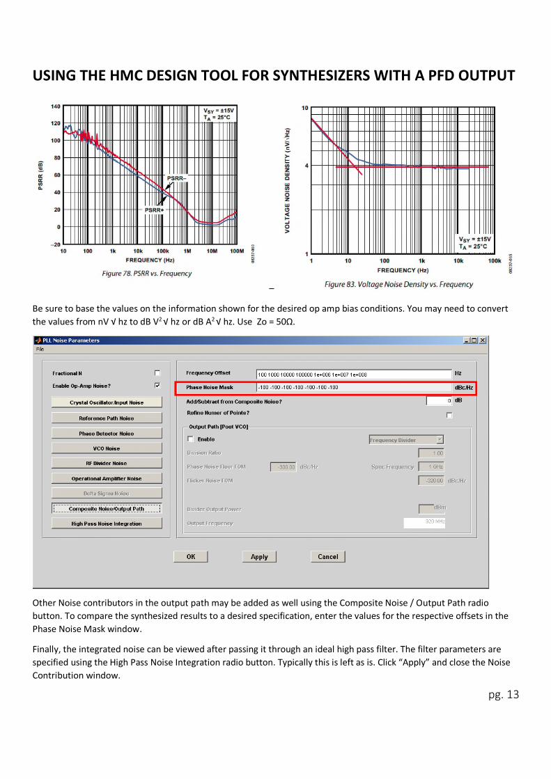
pg. 13
–
Be sure to base the values on the information shown for the desired op amp bias conditions. You may need to convert
the values from nV √ hz to dB V2 √ hz or dB A2 √ hz. Use Zo = 50Ω.
Other Noise contributors in the output path may be added as well using the Composite Noise / Output Path radio
button. To compare the synthesized results to a desired specification, enter the values for the respective offsets in the
Phase Noise Mask window.
Finally, the integrated noise can be viewed after passing it through an ideal high pass filter. The filter parameters are
specified using the High Pass Noise Integration radio button. Typically this is left as is. Click “Apply” and close the Noise
Contribution window.

USING THE HMC DESIGN TOOL FOR SYNTHESIZERS WITH A PFD OUTPUT
pg. 14
MAIN WINDOW
Enter the desired synthesizer parameters into the region shown by the red box above. The Phase Detector Gain when
the PFD Filter type is used will be specified in V / Rad (the output of the HMC439QS16GE is 2V pp).

USING THE HMC DESIGN TOOL FOR SYNTHESIZERS WITH A PFD OUTPUT
pg. 15
FILTER DESIGN
The ‘Filter Design’ radio button allows selection of various loop filter types.
We will need to use the PFD Filter type as shown above.
Next, enter the VCO Input capacitance from the VCO datasheet. C3 will be derived based on this value and the ratio
shown for C3 / Cvco (1000 is typical).
R1 / RL Ratio should be left at 1 as R1 will be derived based on the value we list for RL. RL is equivalent to the 200Ω pull-
up resistor shown on the applications circuits for the HMC439QS16GE. On newer parts these 200Ω resistors were moved
inside the device so although you will still need to specify the value here, you will not populate ‘RL’ on your layout, you

USING THE HMC DESIGN TOOL FOR SYNTHESIZERS WITH A PFD OUTPUT
pg. 16
will still need to populate R1. Another pitfall that is often made is altering the value of RL. This sets the voltage swing
and provides the optimum noise performance so the value should remain at 200Ω. R1 should match this value.
The remaining values will be automatically calculated from the ‘Main’ form. Click ‘Apply’ and close the ‘Loop Filter
Design’ window.
Clicking ‘Compute’ yields the result shown above. Note that C2 is an unrealistically large value due to our narrow loop
bandwidth.

USING THE HMC DESIGN TOOL FOR SYNTHESIZERS WITH A PFD OUTPUT
pg. 17
Increasing the Loop bandwidth yields a more realistic value. After computing use the ‘Set Scale’ buttons to re-scale if
desired. To tweak the performance, check the ‘Fix RC Values’ box. This will calculate the loop response based on the
component values instead of the ‘Desired Bandwidth’ and ‘Desired Phase Margin’ text boxes.
Note that depending on the design, when N = 1 you may see up to a 3dB degradation over the synthesized performance.