vamshi krishna chillara - bogdanst.com · vamshi krishna chillara thesis. an ultra-low-power adpll...
TRANSCRIPT

Electronics
An Ultra-Low-Power ADPLL forWPAN ApplicationsDesign, Implementation, and Validation
Vamshi Krishna Chillara
Mas
tero
fScie
nce
Thes
is

An Ultra-Low-Power ADPLL for WPANApplications
Design, Implementation, and Validation
Master of Science Thesis
For the degree of Master of Science in Electrical Engineeringat Delft University of Technology
Vamshi Krishna Chillara
November 15, 2013
Faculty of Electrical Engineering Mathematics and Computer Science (EEMCS) ·Delft University of Technology

Copyright c© Electrical EngineeringAll rights reserved.
Delft University of TechnologyDepartment of
Electrical Engineering
The undersigned hereby certify that they have read and recommendto the Faculty of Electrical Engineering Mathematics and Computer
Science (EEMCS) for acceptance a thesis entitledAn Ultra-Low-Power ADPLL for WPAN Applications
byVamshi Krishna Chillara
in partial fulfillment of the requirements for the degree ofMaster of Science Electrical Engineering
Dated: November 15, 2013
Supervisor(s):Prof. Dr. Robert Bogdan Staszewski
Dr. Yao-Hong Liu
Reader(s):Dr. Ir. Wouter A. Serdijn
Prof. Dr. Edoardo Charbon
Ir. Ying Wu

Abstract
RF PLLs for frequency synthesis and modulation consume a significant share ofthe total transceiver power, making sub-mW PLLs key to realize ulp WPAN radios.Compared to analog PLLs, all-digital phase-locked loops (ADPLLs) are preferred innanoscale CMOS, as they offer benefits of smaller area, programmability, capabilityof extensive self-calibrations, and easy portability. However, analog PLLs dominatethe ulp arena, since the time-to-digital converter (TDC) of an ADPLL has tradi-tionally been power hungry. In this work [1], an ultra-low power 2.1 GHz – 2.7 GHzfractional-N ADPLL is presented for wireless personal area network (WPAN) applica-tions. A DTC-assisted snapshot TDC and a DC-coupled DCO buffer with a tunablevoltage transfer characteristic (VTC) are proposed to lower the power consumption.The ADPLL prototype fabricated in TSMC LP 40 nm CMOS process consumes only860 µW at 1 V supply, and has a measured rms jitter of 1.71 ps (integrated from1k to 100MHz), leading to a state-of-the-art jitter2-power FoM of -236 dB. Thefrequency modulation capability is also demonstrated with a 2 Mcps HS-OQPSKmodulation for IEEE 802.15.4 (ZigBee) and 1 Mbps GFSK for Bluetooth Smart. Thiswork presents the first-ever wireless ADPLL to break the 1mW barrier and consumesat least five-times lower power compared to state-of-the-art ADPLLs. The presentedlow-power techniques enable the adoption of ADPLLs in the emerging ultra-low-powerapplications.
Master of Science Thesis i Vamshi Krishna Chillara

ii Abstract
Vamshi Krishna Chillara Master of Science Thesis

Acknowledgements
I would like to thank my supervisor, Prof. Robert Bogdan Staszewski, who intro-duced me to this exciting field of Digital-RF. Needless to say, his constant guidance,encouragement, and immense knowledge were indispensable for successful comple-tion of this work. I am glad (rather relieved) that I did not mar his immaculaterecord of first-time silicon success with ADPLLs.I want to thank Dr. Wouter Serdijn, Prof. Edoardo Charbon, and Ying Wu forreading my thesis and serving on my committee.I would like to thank Dr. Kathleen Philips for providing the opportunity to workat imec-nl. My daily-supervisors, Dr. Maja Vidojković and Dr. Yao-Hong Liu, hadbeen of great support and guidance through out, and I cannot thank them enough.Maja got me started, helped me with the layout during the tape-out crunch, and wasalways there for any advice—technical or otherwise. Yao-Hong was the go-to guyfor most part of my work, and we spent a lot of time having detailed discussions onevery conceivable issue. He coordinated this two-student project, and also broughtdelicious home-cooked lunches when we had to work over weekends.I owe special thanks to Bindi Wang for her meticulous design of the TDC and DTC,and importantly, for being a great company during times we had to work long. Ishould thank Xiongchuan (Coby) Huang and Ao Ba for their help in designing theDCO. Ao also designed the PA used in this work. I want to acknowledge the generoussupport of Benjamin Büsze in synthesizing the digital logic. I am grateful to Sandraand Marion for helping with the administrative tasks.Ini and Sangan deserve special mention, for one cannot endure microelectronics atDelft, and remain sane without amazing friends. Also, Satoshi should be thankedfor organizing get-togethers, visits, and ensuring we felt at home amidst all thedutch-eccentricities.Last thanks, as always, goes to my family for their unconditional love and support.My brother has been a great friend and mentor through out my life, and I will alwaysstrive to emulate him. My mom and dad did all they could to ensure I have a betterlife; I am fortunate to have them in my life. I should acknowledge Google Hangoutsfor connecting us from across three continents.
Master of Science Thesis iii Vamshi Krishna Chillara


Table of Contents
Abstract i
Acknowledgements iii
1 Introduction 11-1 Frequency synthesis in wireless transceivers . . . . . . . . . . . . . . . . 1
1-1-1 Metrics of a frequency synthesizer . . . . . . . . . . . . . . . . . 21-1-2 Impact of phase noise on transceiver operation . . . . . . . . . . 3
1-2 PLL based frequency synthesis . . . . . . . . . . . . . . . . . . . . . . . 51-2-1 Charge-pump phase-locked loop . . . . . . . . . . . . . . . . . . 5
1-3 Motivation and thesis objectives . . . . . . . . . . . . . . . . . . . . . . 71-3-1 Target specifications . . . . . . . . . . . . . . . . . . . . . . . . 8
1-4 Research contribution . . . . . . . . . . . . . . . . . . . . . . . . . . . 91-5 Thesis organization . . . . . . . . . . . . . . . . . . . . . . . . . . . . 10
2 All-digital phase-locked loops 112-1 Existing architectures . . . . . . . . . . . . . . . . . . . . . . . . . . . 11
2-1-1 Divider-less ADPLL . . . . . . . . . . . . . . . . . . . . . . . . . 112-1-2 Divider-based ADPLL . . . . . . . . . . . . . . . . . . . . . . . . 132-1-3 Comparison of divider-less and divider-based architectures . . . . 13
2-2 Requirements on TDC and DCO . . . . . . . . . . . . . . . . . . . . . . 142-2-1 Impact of TDC on phase noise . . . . . . . . . . . . . . . . . . . 142-2-2 Impact of DCO on phase noise . . . . . . . . . . . . . . . . . . . 15
2-3 Direct frequency modulation . . . . . . . . . . . . . . . . . . . . . . . . 162-3-1 Two-point frequency modulation . . . . . . . . . . . . . . . . . 16
2-4 Challenges for ultra-low-power applications . . . . . . . . . . . . . . . . 172-4-1 Reducing the TDC detection range . . . . . . . . . . . . . . . . 172-4-2 Lowering the operating frequency of TDC . . . . . . . . . . . . . 18
2-5 DTC-assisted snapshot TDC based ADPLL . . . . . . . . . . . . . . . . . 192-5-1 Phase prediction . . . . . . . . . . . . . . . . . . . . . . . . . . 202-5-2 Snapshotting and CKR generation . . . . . . . . . . . . . . . . . 232-5-3 Low-speed digital logic . . . . . . . . . . . . . . . . . . . . . . . 24
Master of Science Thesis v Vamshi Krishna Chillara

vi Table of Contents
3 RTL design 273-1 RTL design of low-speed digital logic . . . . . . . . . . . . . . . . . . . 27
3-1-1 Finite state machine . . . . . . . . . . . . . . . . . . . . . . . . 283-1-2 TX interface . . . . . . . . . . . . . . . . . . . . . . . . . . . . 293-1-3 TDC readout . . . . . . . . . . . . . . . . . . . . . . . . . . . . 313-1-4 Phase detector . . . . . . . . . . . . . . . . . . . . . . . . . . . 323-1-5 Loop filter—PVT bank . . . . . . . . . . . . . . . . . . . . . . . 343-1-6 Loop filter—Acquisition bank . . . . . . . . . . . . . . . . . . . 363-1-7 Loop filter—Tracking bank . . . . . . . . . . . . . . . . . . . . 36
3-2 System simulation in Verilog . . . . . . . . . . . . . . . . . . . . . . . . 393-3 Estimated power consumption . . . . . . . . . . . . . . . . . . . . . . . 41
4 Circuit design 434-1 Digitally controlled oscillator (DCO) . . . . . . . . . . . . . . . . . . . . 43
4-1-1 Inductor . . . . . . . . . . . . . . . . . . . . . . . . . . . . . . 444-1-2 Active part and biasing . . . . . . . . . . . . . . . . . . . . . . 464-1-3 Capacitor banks . . . . . . . . . . . . . . . . . . . . . . . . . . 474-1-4 Layout . . . . . . . . . . . . . . . . . . . . . . . . . . . . . . . 57
4-2 DCO buffer . . . . . . . . . . . . . . . . . . . . . . . . . . . . . . . . . 594-2-1 Self-biased inverter . . . . . . . . . . . . . . . . . . . . . . . . . 594-2-2 DC coupled buffer with tunable VTC . . . . . . . . . . . . . . . 60
4-3 Divider . . . . . . . . . . . . . . . . . . . . . . . . . . . . . . . . . . . 634-3-1 Transmission-gate based dynamic divider . . . . . . . . . . . . . 634-3-2 Tri-state inverter based dynamic divider . . . . . . . . . . . . . . 644-3-3 Post-layout simulations . . . . . . . . . . . . . . . . . . . . . . 64
4-4 Phase incrementer . . . . . . . . . . . . . . . . . . . . . . . . . . . . . 67
5 Measurements 695-1 ADPLL test plan . . . . . . . . . . . . . . . . . . . . . . . . . . . . . . 695-2 Measurement results . . . . . . . . . . . . . . . . . . . . . . . . . . . . 70
5-2-1 Open-loop DCO measurements . . . . . . . . . . . . . . . . . . . 705-2-2 Loop-locking behavior . . . . . . . . . . . . . . . . . . . . . . . 735-2-3 Spectral purity and phase noise . . . . . . . . . . . . . . . . . . 745-2-4 Direct frequency modulation . . . . . . . . . . . . . . . . . . . . 765-2-5 Power consumption . . . . . . . . . . . . . . . . . . . . . . . . 795-2-6 Performance summary and comparison . . . . . . . . . . . . . . 79
6 Conclusions 816-1 Future work . . . . . . . . . . . . . . . . . . . . . . . . . . . . . . . . 82
A Chip pinout, bonding diagram, and measurement setup 83
B Simulations 87B-1 Simulations of the capacitor banks . . . . . . . . . . . . . . . . . . . . 87
Vamshi Krishna Chillara Master of Science Thesis

Table of Contents vii
Bibliography 93
Glossary 99List of Acronyms . . . . . . . . . . . . . . . . . . . . . . . . . . . . . . 99
Master of Science Thesis Vamshi Krishna Chillara

viii Table of Contents
Vamshi Krishna Chillara Master of Science Thesis

List of Figures
1-1 Low-power transceiver architecture. . . . . . . . . . . . . . . . . . . . . 21-2 Frequency synthesis. . . . . . . . . . . . . . . . . . . . . . . . . . . . . 21-3 Phase noise and spurious tones. . . . . . . . . . . . . . . . . . . . . . . 41-4 Effect of tx phase noise. . . . . . . . . . . . . . . . . . . . . . . . . . 41-5 Effect of LO phase noise on receiver. . . . . . . . . . . . . . . . . . . . 41-6 PLL based frequency synthesizer. . . . . . . . . . . . . . . . . . . . . . 51-7 Simplified block diagram of charge-pump phase-locked loop (CP-PLL). . . 61-8 Benchmark of fractional-N ADPLLs. . . . . . . . . . . . . . . . . . . . . 8
2-1 Architecture of divider-less ADPLL. . . . . . . . . . . . . . . . . . . . . 122-2 Architecture of divider-based ADPLL. . . . . . . . . . . . . . . . . . . . 132-3 Two-point frequency modulation in divider-less ADPLL architecture. . . . 162-4 Principle of phase-prediction to reduce fractional-phase detection range. . 182-5 Top-level block diagram of the ADPLL. . . . . . . . . . . . . . . . . . . 212-6 Idea of digital-to-time converter (DTC) gain calibration [48]. . . . . . . . 222-7 tdc snapshotting and ckr generation. . . . . . . . . . . . . . . . . . . 23
3-1 Top-level block diagram of low-speed logic. . . . . . . . . . . . . . . . . 283-2 FSM of the implemented ADPLL. . . . . . . . . . . . . . . . . . . . . . 293-3 Implementation of tx interface block. . . . . . . . . . . . . . . . . . . 303-4 Implementation of TDC readout block. . . . . . . . . . . . . . . . . . . 313-5 Decoding the output of TDC. . . . . . . . . . . . . . . . . . . . . . . . 323-6 Implementation of phase detector block. . . . . . . . . . . . . . . . . . 333-7 Loop filter—top level block diagram. . . . . . . . . . . . . . . . . . . . 343-8 Loop filter and normalization for PVT bank. . . . . . . . . . . . . . . . . 353-9 Loop filter and normalization for acquisition bank. . . . . . . . . . . . . 373-10 Loop filter and normalization for tracking bank. . . . . . . . . . . . . . . 383-11 First order Σ∆ modulator. . . . . . . . . . . . . . . . . . . . . . . . . . 39
Master of Science Thesis ix Vamshi Krishna Chillara

x List of Figures
3-12 System level ADPLL simulation. . . . . . . . . . . . . . . . . . . . . . . 403-13 System level ADPLL simulation—PVT state. . . . . . . . . . . . . . . . . 403-14 System level ADPLL simulation—acquisition state. . . . . . . . . . . . . 403-15 System level ADPLL simulation—tracking state. . . . . . . . . . . . . . . 40
4-1 RLC model of the LC tank. . . . . . . . . . . . . . . . . . . . . . . . . 444-2 Inductance vs frequency across process corners. . . . . . . . . . . . . . . 454-3 Q-factor vs frequency across process corners. . . . . . . . . . . . . . . . 464-4 Circuit schematic of the implemented DCO. . . . . . . . . . . . . . . . . 474-5 Layout of the active part of the DCO. . . . . . . . . . . . . . . . . . . . 484-6 Switched MOM configuration. . . . . . . . . . . . . . . . . . . . . . . . 494-7 Circuit schematic of the unit cell of PVT bank. . . . . . . . . . . . . . . 504-8 Layout of the PVT bank. . . . . . . . . . . . . . . . . . . . . . . . . . . 514-9 Capacitance range of the PVT bank. . . . . . . . . . . . . . . . . . . . . 514-10 Layout of the acquisition bank. . . . . . . . . . . . . . . . . . . . . . . 524-11 Capacitance range of the acquisition bank. . . . . . . . . . . . . . . . . 534-12 Circuit schematic of the unit cell of tracking bank. . . . . . . . . . . . . 534-13 Circuit schematic of the MSB cell of tracking bank. . . . . . . . . . . . 554-14 Physical layout of the unit cell of tracking bank . . . . . . . . . . . . . . 554-15 Physical layout of the tracking bank. . . . . . . . . . . . . . . . . . . . 564-16 Capacitance range of the tracking bank. . . . . . . . . . . . . . . . . . 564-17 Layout of the DCO. . . . . . . . . . . . . . . . . . . . . . . . . . . . . . 574-18 Transient simulation of the DCO. . . . . . . . . . . . . . . . . . . . . . 584-19 Phase-noise simulation of the DCO. . . . . . . . . . . . . . . . . . . . . 584-20 Self-biased inverter as the DCO buffer. . . . . . . . . . . . . . . . . . . . 594-21 Biasing the self-biased inverter. . . . . . . . . . . . . . . . . . . . . . . 594-22 Tuning the VTC of the inverter. . . . . . . . . . . . . . . . . . . . . . . 604-23 Schematic of the proposed VTC-tunable buffer. . . . . . . . . . . . . . . 614-24 Operation of the buffer across process corners and phase-noise. . . . . . 624-25 Transmission-gate based dynamic CMOS divider. . . . . . . . . . . . . . 634-26 Tri-state inverter based dynamic CMOS divider. . . . . . . . . . . . . . 644-27 Simplified schematic of the implemented divider. . . . . . . . . . . . . . 654-28 Transient simulation of the divider at 1 V and 0.9 V supply. . . . . . . . 654-29 Phase noise of the divider at 1 V and 0.9 V supply. . . . . . . . . . . . . 664-30 Timing waveforms of ckvd2, ckr, and phase incrementer output. . . . 674-31 Circuit schematic of the phase incrementer. . . . . . . . . . . . . . . . . 68
5-1 Chip-micrograph of the ADPLL prototype. . . . . . . . . . . . . . . . . . 695-2 Block diagram of ADPLL test setup. . . . . . . . . . . . . . . . . . . . . 705-3 Measured tuning range of the DCO at 1 V supply. . . . . . . . . . . . . . 715-4 Measured tuning range of the tracking bank of the DCO. . . . . . . . . . 725-5 Measured phase noise of the DCO. . . . . . . . . . . . . . . . . . . . . . 73
Vamshi Krishna Chillara Master of Science Thesis

List of Figures xi
5-6 Measured phase noise of the DCO versus current. . . . . . . . . . . . . . 745-7 Measured settling behavior of the ADPLL. . . . . . . . . . . . . . . . . . 745-8 Output spectrum of the ADPLL for FCW = 37.5. . . . . . . . . . . . . . 755-9 Fractional spur over Bluetooth Smart channels. . . . . . . . . . . . . . . 755-10 Measured phase noise of the synthesizer for FCW = 38.125. . . . . . . . 755-11 Measured phase noise of the synthesizer for FCW = 37.5. . . . . . . . . . 765-12 Measured ZigBee modulation accuracy. . . . . . . . . . . . . . . . . . . 775-13 Measured ZigBee spectrum. . . . . . . . . . . . . . . . . . . . . . . . . 775-14 Measured Bluetooth Smart modulation accuracy. . . . . . . . . . . . . . 785-15 Measured Bluetooth Smart spectrum. . . . . . . . . . . . . . . . . . . . 785-16 Jitter variance-power plot of state-of-the-art PLLs. . . . . . . . . . . . . 80
6-1 FoM versus power consumption of state-of-the-art PLLs. . . . . . . . . . 82
A-1 Bonding diagram of the ADPLL IC. . . . . . . . . . . . . . . . . . . . . 83A-2 Photograph of the test PCB. . . . . . . . . . . . . . . . . . . . . . . . . 85A-3 Photograph of the test bench setup. . . . . . . . . . . . . . . . . . . . 85
B-1 C–V curve of the unit cell of the PVT bank. . . . . . . . . . . . . . . . . 87B-2 Quality factor of the unit cell of the PVT bank. . . . . . . . . . . . . . . 88B-3 C–V curve of the unit cell of the acquisition bank. . . . . . . . . . . . . 88B-4 Quality factor of the unit cell of the acquisition bank. . . . . . . . . . . 89B-5 C–V curve of the LSB cell of the tracking bank. . . . . . . . . . . . . . 89B-6 Quality factor of the LSB cell of the tracking bank. . . . . . . . . . . . . 90B-7 C–V curve of the MSB cell of the tracking bank. . . . . . . . . . . . . . 90B-8 Quality factor of the MSB cell of the tracking bank. . . . . . . . . . . . 91
Master of Science Thesis Vamshi Krishna Chillara

xii List of Figures
Vamshi Krishna Chillara Master of Science Thesis

List of Tables
1-1 Target specifications of the frequency synthesizer. . . . . . . . . . . . . 9
3-1 Estimated power breakdown of the low-speed digital logic. . . . . . . . . 41
4-1 Summary of capacitor banks. . . . . . . . . . . . . . . . . . . . . . . . 56
5-1 Measurement results of capacitor banks at around 2.4 GHz . . . . . . . 725-2 Measured power break-down of the ADPLL. . . . . . . . . . . . . . . . . 795-3 Comparison with the state-of-the-art. . . . . . . . . . . . . . . . . . . . 80
A-1 Chip pinout of the ADPLL prototype. . . . . . . . . . . . . . . . . . . . 84
Master of Science Thesis xiii Vamshi Krishna Chillara

xiv List of Tables
Vamshi Krishna Chillara Master of Science Thesis

Chapter 1
Introduction
Wireless communications have seen an explosive growth in the last decade. Anytimeanyplace connectivity is now a reality with smart phones becoming integral to ourdaily lives. Although proliferation of smart mobile devices will continue to propelthe semiconductor market, many untapped opportunities exist in the realm of short-range low-cost wireless networks. These small, low-cost autonomous sensor-nodeshave applications ranging from health care monitoring to home automation andenvironment sensing. It is these networks of tiny sensor-nodes that have the potentialto trigger the next wireless revolution after cell phones and internet. Low-cost high-volume requirements of these sensor nodes fare well with the integration and scalingtrends of CMOS. However, the autonomous operation requires the power consumptionto be as low as possible. Power budget analysis of such sensor nodes reveals that thewireless transceiver dominates the overall power. This, together with the need forlarge volume, low-cost, highly integrated solutions warrant the need for ultra-low-power RF transceivers in nanometer scale digital CMOS technologies. This thesis isan effort in that direction and deals with the design of an ultra-low power all-digitalphase-locked loop (ADPLL) for frequency synthesis in wireless transceivers.
1-1 Frequency synthesis in wireless transceivers
Figure 1-1 shows a simplified block diagram of a typical low-power transceiver. Alow-IF receiver and direct modulation transmitter are typically the preferred ar-chitectures in low-power low-cost applications owing to their power and cost effi-ciency [2–5].
In a low-IF receiver, the received radio frequency (RF) signal from the antenna isdown-converted to a low intermediate frequency (IF) by a quadrature mixer afteramplification by a low-noise amplifier (LNA). After low pass filtering and boostingthe signal amplitude to the required level by means of a programmable gain amplifier(PGA), the signal is fed to an analog-to-digital converter (ADC). The digitized datais then processed by the digital baseband which recovers the transmitted bits. Onthe transmit side, the digital baseband converts the user data to symbols, which are
Master of Science Thesis 1 Vamshi Krishna Chillara

2 Introduction
Electronics
LNA
PA
PGA
PGA
Mixer Low-pass filter
LOI
LOQ
ADC
ADC
IRX data
QRX data
Frequencysynthesizer TX data
FM
AM
Figure 1-1: Low-power transceiver architecture.
pulse shaped to obtain I and Q digital samples. These I and Q samples are thentransformed to polar form with amplitude and phase components. The frequencydata—obtained from differentiating1the phase data—then modulates the synthesizerwhile the amplitude data controls the power amplifier. Thus, polar architectureavoids the need for up-conversion mixers and instead uses direct modulation, therebysaving power and area. Thus, a frequency synthesizer is an integral part of thetransceiver and plays a key role in both receive path—to generate local oscillator(LO) signal for down-conversion—as well as in the transmit path, for direct frequencymodulation.
1-1-1 Metrics of a frequency synthesizer
A local oscillator (LO) that generates a signal with programmable frequency enablesup/down conversion in a wireless transceiver. A frequency synthesizer is normallyused as it can provide signals with high spectral purity over wide range of fre-quencies. Moreover, it enables direct frequency modulation in polar transmitters.Figure 1-2 shows the functional block diagram of such a frequency synthesizer. A
Electronics
FrequencysynthesizerXTAL
Fref
FCW
Fout
Figure 1-2: Frequency synthesis.
frequency synthesizer takes a low frequency clean reference from a crystal oscillator2
1implemented as difference between consecutive samples.2On chip replacements for crystal oscillators such as thermal diffusivity based [6] and MEMS
based [7] references is an active area of research but crystal based references currently dominate [8].
Vamshi Krishna Chillara Master of Science Thesis

1-1 Frequency synthesis in wireless transceivers 3
as an input and generates an output signal with a frequency determined by thefrequency command word (FCW). Some common metrics to gauge the performanceof a frequency synthesizer are discussed here.
Frequency tuning range and resolution
This denotes the range of frequencies that the synthesizer can generate with accept-able spectral purity and resolution. For instance, a frequency synthesizer designed fora 2.4 GHz Bluetooth Smart transceiver should cover the frequencies from 2.402 GHzto 2.480 GHz with a step of 2 MHz. Moreover, the accuracy with which the requiredchannel frequency can be acquired is also crucial and is specified as parts-per-million.Variations over process, voltage, and temperature (PVT) should be considered whileformulating the synthesizer specifications.
Channel switching time
Another important constraint on the synthesizer is its switching time—the time ittakes to switch from one channel to another with a required accuracy. This canbe crucial for some applications requiring fast switching such as frequency hoppingspread spectrum. Moreover, the PLL consumes more power in the transient statecompared to the locked state. Thus, fast switching helps to save power in ultra-low-power applications such as Bluetooth Smart.
Spectral purity
The required spectral purity is usually specified as a spectral mask that the syn-thesizer should satisfy. Both random and periodic fluctuations corrupt the spectralpurity of a frequency synthesizer. The output of a frequency synthesizer can berepresented in time-domain by Eq. (1-1).
v(t) = A sin(ωct+ ψ(t)) (1-1)
where A represents the amplitude of the synthesized signal with frequency ωc. ψ(t)captures the phase fluctuations. The impact of amplitude noise is generally neglectedas it can be alleviated by a limiter circuit. Phase fluctuations in turn are dividedinto random and periodic variations as shown in Eq. (1-2).
ψ(t) = ∆ψ sin(ωmt) + φ(t) (1-2)
The first term denotes the periodic variations, which appear as a spurious tone at afrequency ωm from the carrier. The random fluctuations, φ(t), manifest themselvesas a noise-skirt around the desired frequency (see Figure 1-3).
1-1-2 Impact of phase noise on transceiver operation
Both the spurious tones and the noise skirt degrade the performance of the transceiver.The spot value of the phase noise spectrum at a particular frequency and the integral
Master of Science Thesis Vamshi Krishna Chillara

4 Introduction
Electronics
ωc
Noise-skirt
spurspur
ωm ωm
ω
Figure 1-3: Phase noise and spurious tones.
of phase spectral density over a frequency range can both impair the performanceof the transceiver. On the transmit side, noise-skirt on the LO signal can make it apotential interferer (blocker) to a near-by receiver detecting a signal in the adjacentfrequency channel (see Figure 1-4).Figure 1-5 shows the impact of the phase noise of the frequency synthesizer on thereceiver in the presence of a large blocker in the near-by frequency channel. If the
Electronics
ω
Near-by TXWantedsignal
Figure 1-4: Effect of tx phase noise.
Electronics
signal
blocker
ωRF + ωm ωωRF ω
ωLO ω
ωIF ωIF + ωm
blocker
Figure 1-5: Effect of LO phase noise on receiver.
LO is ideal and has a spectrum of Dirac delta function, δ, then the down-convertedblocker is at offset ωm from the wanted signal and hence can be filtered off. However,if LO signal has a phase-noise skirt or a spectral tone at that offset, the blocker and
Vamshi Krishna Chillara Master of Science Thesis

1-2 PLL based frequency synthesis 5
wanted signal are down-converted to the same IF frequency, thereby degrading thesignal-to-noise ratio (SNR).
1-2 PLL based frequency synthesis
Although other methods such as direct digital synthesis or look-up table synthesisexist, phase-locked loop (PLL) based indirect frequency synthesis is widely used inwireless applications owing to its spectral purity and energy efficiency. Figure 1-6depicts a simple block diagram of a PLL based frequency synthesizer.
PLL is a negative feedback system that ensures that the phase of the desired outputsignal is locked to that of a known stable reference. The phase detector compares thephase of the reference signal with the output signal and generates the phase error.This phase difference is processed by the loop filter—to set the loop dynamics—andis then used to control the oscillator. In the steady state, the error signal in the loopis forced to a constant value ensuring that the phases of two signals are locked andhence the frequencies.3 In some implementations, a frequency divider is placed inthe feedback path so that a high frequency signal can be generated from a lowerreference frequency.
The frequency synthesis in wireless transceivers is dominated by charge-pump phase-locked loops (CP-PLLs) and all-digital phase-locked loops (ADPLLs), which differin the implementation of the aforementioned building blocks. With the advent ofnano-scale CMOS, ADPLLs have begun to supplant the traditional CP-PLLs in mostapplications.
Electronics
Loop filter
phasedetectorFref
Frequencydivider
Fdiv
Controlledoscillator
OTW FLO
Figure 1-6: PLL based frequency synthesizer.
1-2-1 Charge-pump phase-locked loop
Figure 1-7 shows a simplified block diagram of the conventional CP-PLL. The con-trolled oscillator of Figure 1-6 is implemented as a voltage-controlled oscillator(VCO)—controlled by an analog input voltage. The phase frequency detector (PFD)compares the phase of the reference signal and the divided down output signal, Fdiv,to generate an up/down pulse with a width proportional to the phase error. The
3frequency being the derivative of phase, a constant phase difference translates to zero frequencydifference.
Master of Science Thesis Vamshi Krishna Chillara

6 Introduction
output of the phase detector controls the magnitude and direction of the charge-pump current that is pumped into or out of the loop filter. The passive loop-filterconverts this current into a tuning voltage for the VCO while suppressing the noisefrom the reference signal and the phase frequency detector. The output frequencyof the VCO is adjusted such that the steady-state phase difference becomes constantand the output frequency is N times the input reference frequency.In integer-N synthesizers, the reference frequency limits the frequency resolution. Afine frequency resolution requires a small reference frequency which limits the maxi-mum loop-bandwidth that can be attained owing to the concerns of loop stability [9].Loop-bandwidth is usually chosen not greater than one-tenth of the reference fre-quency. A wide loop bandwidth might be needed for higher suppression of oscillatorphase noise or for faster switching speeds. Also, a small reference frequency needsa large multiplying factor N. Noise on the reference signal is amplified by N2 andhence a very large value of N is not desired.To decouple this bandwidth-resolution trade-off, fractional-N synthesizers evolved.The division ratio of the multi-modulus divider toggles between two integer valuese.g., N and N+1, to achieve the required fractional division on average. The dividercontrol is generated by a Σ∆ modulator to scramble the control pattern so that theresulting quantization noise is high-pass shaped. Consequently, Σ∆ control of thedivider ratio enables a fine frequency resolution with a large reference frequency.However, the bandwidth cannot be too large since the quantization induced phasenoise should be sufficiently filtered.
PFDFREF
VDD
IP
IN
up
down
Charge-pump
C2 R1
C1
Loop filter
÷(N + b) Frequencydivider
Fvco
Σ∆modulator
b(t)
Fdiv
Phase/freqeuncydetector VCO
Figure 1-7: Simplified block diagram of charge-pump phase-locked loop (CP-PLL).
Implementation difficulties in nanoscale CMOS
CP-PLLs with sub-mW power consumption have been realized for use in ultra-low-power applications [5]. However, the analog intensive nature of the CP-PLL makes
Vamshi Krishna Chillara Master of Science Thesis
1-3 Motivation and thesis objectives 7
its implementation difficult in advanced process nodes. Technology scaling shrinksthe transistor dimensions to enable high integration densities. Supply voltages arealso reduced to limit the electric fields so as to ensure reliable operation. However,this supply reduction makes it challenging to design traditional analog circuits suchas a cascoded current source used in the charge-pump. Moreover, short channeleffects such as drain-induced barrier lowering (DIBL) lead to reduced drain-sourceimpedance of the transistor further complicating the design of current sources. Also,the smallest transistor dimensions are usually not used in the charge-pump design tominimize noise and to achieve good matching between up and down current sources.Hence a charge-pump occupies a significant area. Also, since the passives do notscale well with the technology, the loop-filter used in CP-PLL occupies large area,increasing the overall system costs. In addition, the reduced gate-oxide thickness inthe nanoscale CMOS technologies results in significant current leakage through theintegration capacitor of the loop-filter. This leakage current increases the total PLLjitter, thereby degrading the performance.
1-3 Motivation and thesis objectives
The need for low-power low-cost transceivers in large volumes favors the realizationin the most advanced CMOS node available. The problems with analog design in low-voltage nano-meter scale CMOS processes and the possibility to integrate RF front-end with baseband processor favors the digitally intensive approach. Furthermore,a digital intensive approach provides numerous other benefits—better testability,reconfigurability, lower area, and high degree of integration. Moreover, the digitalapproach allows for extensive calibrations; for instance it is possible to track andcorrect the variations of the digitally controlled oscillator (DCO) gain over process,voltage, and temperature (PVT) [10]. This enables to accurately implement two-pointfrequency modulation required for a polar transmitter.
Accordingly, a digitally intensive PLL architecture called ADPLL emerged for fre-quency synthesis in wireless applications. Since its inception in [11], ADPLLs havegarnered the attention of numerous researchers because of their financial benefits andamenability to scaling. ADPLLs for frequency synthesis in different wireless standardsnamely Bluetooth, GSM, and EDGE have been successfully demonstrated [12–14]with a performance comparable to or even better than that of conventional charge-pump phase-locked loops (CP-PLLs). DCO and time-to-digital converter (TDC) be-ing the main bottle-necks justifiably have seen a number of efforts to counter thelimitations arising from their finite resolution. While [15–17] improve the DCO’sperformance, [18–21] address the problems that arise from TDC non-idealities. Thefractional spurs that impede the realization of a wide-band ADPLL are the focusof [22,23]. Thanks to these improvements, nearly one-third of the new mobile phonesproduced use ADPLLs [24].
In contrast, ADPLLs are hardly used in the ultra-low power arena with charge-pumpPLLs dominating the frequency synthesis in these transceivers [25–29]. This is evidentfrom Figure 1-8 which shows a plot of fractional-N ADPLLs published in the last fiveyears at ISSCC and VLSI symposium. The published works are plotted with powerconsumption in mW as abscissa and the jitter variance in ps2 as the ordinate. The
Master of Science Thesis Vamshi Krishna Chillara

8 Introduction
jitter2-power FoM4 is also indicated in the graph. It can be noticed that there are nofractional-N ADPLLs in the sub-mW vicinity, a key requirement for Bluetooth Smartand ZigBee applications. The main objective of this thesis is to break the sub-mWbarrier for ADPLLs so as to enable their adoption in ultra-low-power applications.The targeted specifications and scope of this thesis are discussed in the next section.
Figure 1-8: Benchmark of fractional-N ADPLLs.
1-3-1 Target specifications
The specifications of the targeted frequency synthesizer are shown in Table 1-1. Inaddition to generating the LO signal with the required frequency, this ADPLL shouldalso act as a direct frequency modulator in the transmitter path. Accordingly, anADPLL with a two-point modulation capability satisfying the tabulated specificationsis targeted.This all-digital synthesizer designed in 40 nm digital CMOS technology targets Blue-tooth Smart and ZigBee standards around the 2.4 GHz ISM band. It is desirable ifthis very synthesizer can also support 400 MHz medical implant communication ser-vice (MICS) applications. The MICS standard has two bands of frequencies: 402–405MHz and 420–450 MHz. Hence, the synthesizer is targeted to cover the frequencyrange of 2.4–2.7 GHz (400–450 MHz after division by 6) to accommodate all thethree aforementioned standards. In addition, the synthesizer should be able to han-dle data rates of up to 1 Mbps for Bluetooth Smart when acting as a frequency
4FoM = 10log10
((σ2
jitter
)∗(
P1mW
))[30]
Vamshi Krishna Chillara Master of Science Thesis

1-4 Research contribution 9
Table 1-1: Target specifications of the frequency synthesizer.
Parameter RequirementFrequency range 2.4–2.7 GHzFrequency accuracy 60 KHzSwitching time 40 µsPhase noise @ 1 MHz offset -110 dBc/HzIntegrated RMS phase error 2
Modulation data rate 1 MbpsReference frequency 32 MHzPower consumption <1 mWTechnology 40 nm digital CMOS
modulator. Finally, sub-mW power consumption is crucial to accommodate its usein the autonomous sensors deployed in wireless personal area networks (WPANs) orwireless body area networks (WBANs).
1-4 Research contribution
It is clear from the earlier discussion that the analog charge-pump phase-locked loops(CP-PLLs) dominate the ultra-low-power landscape. ADPLLs not only ease the designchallenges in advanced process nodes but also facilitate additional benefits thataccrue from digitization. However, ADPLLs have not been explored for the ultra-low-power applications, which require sub-mW power consumption. This work presentsthe first-ever multi GHz sub-mW fractional-N ADPLL by using a combination ofdigital-to-time converter (DTC) and TDC for fractional phase detection.
A TDC in a conventional ADPLL [31] needs to cover one full DCO period sensing theDCO clock at its full rate, thus consuming several mW. In this work, TDC snapshot-ting is implemented to reduce the sampling rate to FREF, while the DTC reducesthe detection range to less than one-tenth of the DCO clock period, leading to asignificant power reduction.
In addition, a power efficient DCO buffer with a tunable voltage transfer character-istic (VTC) is presented. It is DC coupled to the low-swing output of the DCO toavoid driving bulky resistor-biased decoupling capacitors. This approach reduces theoverall power consumption of the DCO plus buffers.
In this two-student ultra-low-power ADPLL project at imec-nl, my work deals withthe system level analysis of ADPLL, rtl and back-end design of low-speed digitalcircuitry, and circuit-level design of DCO and other high frequency blocks. The TDC,DTC, and the necessary calibration circuitry are designed by a colleague, Bindi Wang.A silicon prototype that can support Bluetooth Smart and ZigBee standards whileconsuming just 860 µW is implemented to demonstrate the feasibility of adaptingADPLLs for frequency synthesis in ultra-low power transceivers.
Master of Science Thesis Vamshi Krishna Chillara

10 Introduction
1-5 Thesis organization
This thesis is organized as follows. Chapter 2 begins with a background on ADPLLswhile reviewing the current state-of-the-art and highlighting the challenges in adapt-ing ADPLLs for ultra-low-power applications. Then the DTC assisted snapshot TDCbased ADPLL implemented in this work is presented. Chapter 3 describes the rtldesign of this ADPLL. The circuit design of DCO and other high speed blocks—divider-by-2, phase incrementer, and DCO buffer—is described in Chapter 4 alongwith simulation results. The measurement set-up, pcb layout, and the measurementresults of the implemented silicon prototype are presented in Chapter 5. Chapter 6is reserved for conclusions and provides suggestions for future work.
Vamshi Krishna Chillara Master of Science Thesis
Chapter 2
All-digital phase-locked loops
This chapter reviews the common architectures of all-digital phase-locked loops(ADPLLs) from the literature. The power consumption of each of these architecturesis analyzed to identify the power-hungry blocks. The possible solutions to reduce thepower at architectural level are explored. Finally, the digital-to-time converter (DTC)assisted snapshot time-to-digital converter (TDC) based ADPLL implemented in thiswork is described.
2-1 Existing architectures
Digital processing is cheaper, faster, and consumes less power in advanced CMOSnodes. However, scaling is less attractive for analog circuits as they are limited bythe electronic noise and low supply voltages make it difficult to meet the accuracyrequirements. ADPLLs evolved to address the challenges of implementing the tradi-tional charge-pump phase-locked loops (CP-PLLs) in advanced process nodes.In an ADPLL all the analog blocks of the CP-PLL are replaced either by their dig-ital equivalents or by mixed signal blocks with digital interfaces at the input andoutput. A voltage-controlled oscillator (VCO) of the conventional CP-PLL is replacedby a digitally controlled oscillator (DCO), which deliberately avoids any analog tun-ing. The DCO produces a frequency proportional to its input digital word plus anoffset. The charge-pump/phase-frequency detector combination got replaced by aTDC, which digitizes the time difference (phase) between its input signals. Since thephase error is digitized, a bulky passive loop filter of the CP-PLL can be replacedby a compact digital one, resulting in considerable cost savings. A review of currentliterature reveals various implementations to realize an ADPLL, mostly differing inthe way phase to digital conversion is achieved. They can be broadly classified intothe following two types: divider-less and divider-based ADPLLs.
2-1-1 Divider-less ADPLL
This is the architecture that triggered the research in digital-intensive frequencysynthesis for wireless transceivers and is first presented in [31]. Figure 2-1 shows
Master of Science Thesis 11 Vamshi Krishna Chillara

12 All-digital phase-locked loops
a simplified block-diagram of the divider-less ADPLL [32]. The output frequencytermed as the variable frequency, Fv, is set by the frequency command word (FCW).
FCW = FvFREF
(2-1)
Equivalently, FCW denotes the number of clock cycles of variable clock (CKV) inone reference clock. Hence, accumulating the FCW at reference rate provides thereference phase (ΦR) that is normalized to CKV clock period. The variable phase,ΦV , is obtained by counting the number of output clock cycles. Phase incrementergives the integer part of the variable phase, ΦV_int. A TDC is used to detect thephase with a resolution finer than one integer cycle.A typical TDC consists of a chain of delay elements that delay the CKV signal. Thedelayed versions of the CKV are sampled by fref to obtain the time delay betweenthe edges in terms of number of delay elements [18]. Hence the resolution of thefractional phase detection is limited by the intrinsic delay of the unit cells in theTDC. The fractional phase is obtained by normalizing the output of the TDC to theCKV period.The variable phase and reference phase, which are available as digital words cannow be subtracted by digital logic to generate the phase error. This phase erroris passed through a digital loop filter to obtain the oscillator tuning word (OTW).OTW controls the DCO frequency in a negative feedback configuration such that thephases of the CKV and reference clock fref are either equal or have a constantdifference in the steady state, depending on the type of loop. The frequency of thevariable clock (CKV) is hence equal to FCW times the reference frequency.
FREFTDC
DCOOTW
DLF
Phase Incrementer
Σ
CKR
ΦR
ΦV
ΦE
ΦV_int
ΦV_frac
CKVFCW
Figure 2-1: Architecture of divider-less ADPLL.
Since the clock signals CKV and fref are asynchronous, re-timing is needed toavoid metastability. The re-timed reference clock CKR is generated by sampling thereference clock fref with the variable clock (CKV). Since this re-sampling itself mayintroduce metastability, sampling is done both at the rising edge and the falling edgeof CKV, and the one farthest from the metastability is picked [32]. The re-timedreference clock CKR is then used as the clock for the low frequency digital logic:phase detector, digital loop filter, and gain normalization blocks.
Vamshi Krishna Chillara Master of Science Thesis

2-1 Existing architectures 13
2-1-2 Divider-based ADPLL
The divider-based ADPLL architecture, shown in Figure 2-2, is an exact block-by-block replacement of the analog blocks in a traditional CP-PLL with their digitalequivalents. In this architecture, the variable clock (CKV) is passed through a frac-tional divider before it is fed to the TDC. The required output frequency is set bythe divider ratio. To realize a fractional division ratio, a Σ∆ modulator dithers thedivider ratio between two integer values. The TDC compares the time difference be-tween the significant (rising or falling) edges of the stable reference clock fref andthe divided down output clock Fdiv to generate the phase error directly as a digi-tal word. After passing through a digital filter, the phase error controls the DCOfrequency to align it to the reference clock.
FREF TDC
DCOOTW
DLF
Multi-modulus divider
ΣΔFCW
Figure 2-2: Architecture of divider-based ADPLL.
2-1-3 Comparison of divider-less and divider-based architectures
The phase incrementer and the divider play a similar role and consume comparablepower and area, leading to a similar performance in either architecture. However,multi-modulus divider is accompanied with fractional spurs requiring additionalcircuitry to mitigate them [33]. Moreover, divider-based architectures do not operatein phase-domain and hence should be realized as type-II1 systems to ensure thedivided down CKV and fref edges are closely aligned. On the other hand, thedivider-less architectures [31,34] operate in the phase-domain but both the TDC andphase incrementer operate at the high output frequency (typically in the GHz range)consuming significant power. The reduced operating frequency of TDC in a divider-based architecture is offset by its increased range requirement—one reference clockperiod—as opposed to one CKV duration in a divider-less architecture. Thus, ineither architecture, TDC consumes a significant power. Section 2-4 explores differentapproaches in the literature to tackle this issue.
1type indicates the number of poles at the origin
Master of Science Thesis Vamshi Krishna Chillara

14 All-digital phase-locked loops
2-2 Requirements on TDC and DCO
Like any mixed-signal system, ADPLL also suffers from the effects of the inevitablequantization noise resulting from analog-to-digital and digital-to-analog conversion.The TDC which converts the analog phase of the CKV to a digital word limits the in-band phase-locked loop (PLL) noise, while the DCO that converts the digital controlword to an analog signal with desired frequency affects the out-of-band noise. For-tunately, both the TDC resolution—usually limited by the inverter delay—and theDCO frequency step improve with technology scaling and hence the performance ofthe ADPLL improves with each advanced node. The requirements on the resolutionof TDC and DCO for targeted applications are calculated here.
2-2-1 Impact of TDC on phase noise
The finite resolution of TDC results in quantization noise whose power is given byEq. (2-2) [35], where ∆TDC is the quantization step of the time-to-digital converter(TDC).
σ2t = ∆2
TDC/12 (2-2)This noise is distributed over the frequency band (0,fs
2 ), where fs is the samplingfrequency which is the reference frequency, fR, of the ADPLL. By normalizing it tothe unit interval and multiplying by 2π radians phase noise is obtained [32].
σΦ = 2π σtTv
(2-3)
Assuming an ideal TDC, the noise distribution can be considered white giving riseto a single-sided noise spectral density of
L = σ2ΦfR
(2-4)
From Eq. (2-3) and Eq. (2-4), the single sided phase noise of the ADPLL due toquantization of TDC is given by
L = (2π)2
12
(∆TDC
Tv
)2 1fR
(2-5)
This noise from the TDC has a low pass transfer function and hence dominatesthe in-band PLL noise. In addition to the quantization noise, the finite TDC stepand mismatch between the delay elements also result in spurs at the frequency,FCWfrac ∗ FREF , further degrading the phase noise of the ADPLL [22].In the TSMC 40 nm process in which the targeted synthesizer is implemented, aninverter delay of 20 ps is achievable without consuming too much power. For thisvalue of ∆TDC = 20 ps, the in-band PLL noise floor given by Eq. (2-5) is equalto -95 dBc/Hz with 2.7 GHz operating frequency. This value is sufficient for thetargeted applications and hence a delay-line based TDC suffices. Note that, it ispossible to achieve sub-inverter delay resolution, although at the expense of increasedpower consumption. In [19] time amplification is used to achieve sub-ps resolutionbut consumes a staggering 60 mW power. Vernier delay-line based architecture [36]uses the difference between individual delay elements to achieve fine resolution butrequires a large number of cells and hence consumes a lot of power.
Vamshi Krishna Chillara Master of Science Thesis

2-2 Requirements on TDC and DCO 15
2-2-2 Impact of DCO on phase noise
DCO is the core of the ADPLL and produces an output frequency proportional to itsinput digital word in addition to an offset. The frequency resolution of the DCO alsoadds additional quantization noise which can be modeled with white noise spectralcharacteristics provided the input tuning word spans multiple quantization levels.The variance of the quantization error in output frequency is then given by
σ2f = ∆f 2
res/12 (2-6)
Since this phase noise power is spread uniformly from DC to Nyquist frequency, thesingle sided spectral density is given by
12S∆f =
σ2f
fR(2-7)
This can be converted to phase variation by multiplying the DCO’s frequency tophase conversion transfer function, 2π
s. The single-sided phase noise power spectral
density at the output is then given by
L(∆f) = 112
(∆fres∆f
)2 1fR
(2-8)
Since the DCO input tuning word is held constant between two different values, thewhite noise assumption is not fully justified. Hence, the above equation is multipliedby sinc function to account for the zero-order hold operation on the input tuningword of DCO [32].
L(∆f) = 112
(∆fres∆f
)2 1fR
(sinc
∆ffR
)2(2-9)
The quantization noise of the DCO has a 20 dB/decade attenuation, similar to thatof the up-converted thermal noise from the oscillator. As long as this quantizationnoise is kept sufficiently low compared to the inherent phase noise of the oscillator(resulting from thermal and flicker noise of active part or the passive LC tank), theoverall phase noise is not significantly affected. The noise from the DCO is high-pass filtered by the loop and hence has a band-pass characteristic, degrading theout-of-band phase noise of the synthesizer.
A spot noise of -110 dBc/Hz at 1 MHz offset from the carrier frequency is targetedindicating that the phase noise from the DCO quantization should be lower than-120 dBc/Hz. A 50 kHz accuracy is required in channel selection, which correspondsto a DCO quantization noise of -112 dBc/Hz from Eq. (2-9), which is comparableto the targeted phase noise. Hence a 5-bit Σ∆ modulator is used to dither the DCOcontrol word to minimize the quantization noise [17]. In this way, the quantizationstep is reduced to ∆fres/25 and so is the quantization noise. However, the Σ∆-modulator itself introduces spurs somewhat limiting its improvement. Either a highdithering rate or higher order dithering can be employed to counter the issue ofspurs.
Master of Science Thesis Vamshi Krishna Chillara

16 All-digital phase-locked loops
2-3 Direct frequency modulation
Direct frequency modulation of the frequency synthesizer simplifies the transmitterarchitecture, saving power and area. In traditional fractional-N synthesizers, thedivider ratio is modulated by the TX data, achieving the desired frequency deviation.However, the maximum rate of modulation is limited by the loop bandwidth as themodulation signal is filtered by the low-pass characteristic of the PLL. A narrowloop bandwidth is usually chosen to minimize the high frequency quantization noiseinjected by the Σ∆ divider as well as to filter off the noise from phase detector or thereference clock. Thus it is difficult to achieve high data rates by directly modulatingthe divider ratio. To overcome this issue, techniques such as pre-emphasis [37] andtwo-point modulation [38,39] are used.In the approach using pre-emphasis, the frequency control is multiplied by inverseof the PLL transfer function to compensate the low-pass filtering by the loop. How-ever, it requires accurate knowledge of the loop transfer function to ensure the pre-emphasis does not distort the transmission data. In two-point modulation method,the modulation data is added directly to the oscillator control signal in addition tothe divider. If the oscillator gain is accurately known, this method removes the loopdynamics from the transmitted data path. The digital implementation of the PLLeases the implementation challenges of both these approaches. However, since thepre-emphasis method needs extra hardware it is not preferred.
2-3-1 Two-point frequency modulation
Figure 2-3 shows the implementation of the two-point modulation in the divider-lessADPLL architecture. The modulation data is added to the FCW in the low frequency
FREFTDC
DCOOTW
DLF
Phase Incrementer
Σ
CKR
ΦR
ΦV
ΦE
ΦV_int
ΦV_frac
CKVFCW
TX data
Low frequency High frequency
gain
Figure 2-3: Two-point frequency modulation in divider-less ADPLL architecture.
path and directly to the DCO control word in the high frequency path. The scalingfactor in the high-frequency path ensures that the LSB of the modulation datacorresponds to same frequency step in both high and low frequency paths. Thestep in the low-frequency path is set accurately by the reference frequency and is
Vamshi Krishna Chillara Master of Science Thesis

2-4 Challenges for ultra-low-power applications 17
independent of the variations in process, voltage, and temperatures (PVTs). On theother hand, the frequency step of the high frequency path depends on the resolutionof DCO, KDCO, and hence is different to that of the low-frequency path.
When the modulation data increases, the frequency of the DCO and hence the vari-able phase, ΦV , becomes higher. On the low-frequency path, the FCW is also in-creased which increases the reference phase, ΦR, keeping the phase error unchanged.However, the calculation of the gain factor on the high frequency path of the TXdata requires the knowledge of the DCO gain, KDCO. It can be calculated just-in-timeas discussed in [10]. Since the OTW is available as a digital signal, the change in OTWfor a known deviation in frequency can be observed to estimate the value of KDCOover PVT variations. Thus ADPLL can perform direct frequency modulation witha data-rate independent of the loop band-width while consuming little additionalhardware.
2-4 Challenges for ultra-low-power applications
DCO and TDC consume most of the power in an ADPLL. The power consumptionof DCO depends on its phase noise requirements, and hence can be scaled down inshort-range wireless applications. The design of DCO is discussed in Chapter 4. Onthe other hand, the power consumption of TDC is large, mainly owing to its highfrequency operation or large range requirement depending on the architecture.
The similarity of TDC to that of an analog-to-digital converter (ADC) inspired re-search in the lines of Σ∆ data-conversion. However, a coarser TDC resolution re-quirement does not necessarily translate to lower power beyond that available fromminimally sized inverter delays. As a result, Σ∆ frequency discriminator based ar-chitectures [40, 41] do not help unless a bang-bang phase detector is adopted orsub-inverter delay resolutions are required. Also, this approach does not take ad-vantage of the high resolution inverter delays available in the advanced CMOS nodesand expends considerable power in digital processing. A fine resolution TDC allowswide loop bandwidth, thereby filtering more noise from DCO. Since the power con-sumption of DCO is proportional to its phase noise, total ADPLL power can thus bereduced for a given jitter requirement.
In this work, the techniques to reduce the required phase detection range and oper-ating frequency of TDC are explored instead and are discussed here.
2-4-1 Reducing the TDC detection range
TDC needs to cover a range equal to the CKV period with a fine resolution, therebyconsuming considerable power. A bang-bang phase detector is adopted in [42] toreplace the TDC, thereby alleviating the issue of large range requirement. A bang-bang phase detector is essentially a D flip flop determining whether the referencesignal leads or lags the divided down signal. The spurs that are inherent to the bang-bang phase-locked loops (BBPLLs) are minimized by operating it in the random-noiseregime. To achieve this, a true fractional divider using a 10-bit DTC is proposed.
Master of Science Thesis Vamshi Krishna Chillara

18 All-digital phase-locked loops
Compared to a TDC, DTC consumes less power as it does not need power-hungrysense-amplifier based flip-flops [18] required by a TDC. That architecture achievesan impressive figure-of-merit (FoM)2 of -238 dB while consuming 4.5 mW. However,the integrated jitter cannot be traded to achieve the sub-mW power levels requiredfor our targeted applications as it would mean moving away from the random-noiseregime, thereby exacerbating the issue of spurious tones resulting from limit cycles.Moreover, the loop bandwidth of that circuit depends on the noise at the input ofthe bang-bang phase detector and hence additional circuitry is required for loopbandwidth regulation and frequency acquisition.A divider-less ADPLL with DTC and a bang-bang phase detector is presented in[43]. In [44], the authors propose to use the DTC in order to reduce the requiredTDC range rather than replacing it by a bang-bang phase detector. In both thesearchitectures, the accumulated value of fractional FCW is used to delay the referencesignal fref such that the delayed reference signal, frefdly is almost aligned to theCKV once the loop is locked. This idea of phase prediction is depicted in Figure 2-4for the case when FCW = 2.25. As can be seen, the required delay to align the FREFedge to the next CKV edge can be obtained by subtracting the accumulated value offractional FCW from 1. The delayed reference signal and the CKV can be then fed tothe narrow-range TDC, the output of which directly gives the fractional phase error.This approach helps in reducing the TDC range by as much as ten times.
FCW = 2.25
0 1 2 543 106 7 8 9 1211
0 2.25 4.5 6.75 9 11.25
CKV edges
FREF edges
Delay needed0 0.75 0.5 0.25 0 0.75
Figure 2-4: Principle of phase-prediction to reduce fractional-phase detection range.
In yet another approach [45], the quadrature phases of the DCO are used to reducethe operating range of TDC. Again, the accumulated value of FCWfrac is used toselect one of the four CKV phases that is closest to the FREF signal. In this way,the required detection range is reduced to one-fourth of CKV period. However, theTDC is clocked at CKV frequency (usually in the order of GHz), thereby increasingthe power consumption.
2-4-2 Lowering the operating frequency of TDC
The TDC compares the phase difference between the CKV signal and fref andhence operates at high frequency, consuming significant power. However, the phase
2FoM = 10log10
((σ2
jitter
)∗(
P1mW
))[30]
Vamshi Krishna Chillara Master of Science Thesis

2-5 DTC-assisted snapshot TDC based ADPLL 19
difference is calculated only close to the rising edge of fref i.e., the TDC needs tooperate only at the reference rate, typically tens of MHz. This is the basis of thetime-windowed TDC based architecture presented in [46] where the TDC is gatedto reduce its operating frequency and hence power consumption. However, this ap-proach requires a TDC with a detection range equal to the CKV period and hencecannot be combined with one of the methods that reduce the detection range. In [44],DTC based phase-prediction is used to simultaneously reduce the operating frequencyand detection range. Since the phase-prediction maintains a fixed phase differencebetween the frefdly and CKV signals, the first CKV pulse after the rising edge offrefdly is picked and is fed to the TDC for phase detection. In this way, total powerconsumption can be reduced by FCW times—typically on the order of 30–40 fromthe reduced operating frequency and nearly ten times from the reduced detectionrange.
2-5 DTC-assisted snapshot TDC based ADPLL
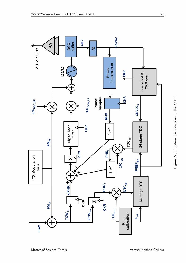
Figure 2-5 depicts the top-level block diagram of the ADPLL with two-point frequencymodulation capability designed in this work. The blocks with gray background—TDC, DTC, snapshotting, KDTC calibration, and power amplifier (PA)—are designedby colleagues at imec-nl and the description of their implementation is not a partof this thesis. The blocks with blue background are the analog/high-speed blocksthat warrant custom design whose circuit level implementation and layout are de-scribed in Chapter 4. The remaining blocks comprise the low-speed digital logicresponsible for processing the phase information to generate the appropriate controlsignals for the DCO. The functional description of the implemented low-speed digitalblocks is provided in this section. The detailed rtl-level description is deferred untilChapter 3.
A divider-less ADPLL architecture with a difference mode phase detector [32] is used.To meet stringent sub-mW PLL power constraints, three low-power techniques areemployed:
1. The biggest power-saving is obtained by using a DTC assisted snapshot TDCfor fractional phase detection. DTC helps in reducing the detection range ofDTC by using the principle of phase-prediction described in Section 2-4-1.Snapshotting reduces the operating frequency to reference rate.
2. Secondly, a power efficient DCO buffer with a tunable voltage transfer char-acteristic (VTC) is used to isolate the DCO from load variations in PA as wellas to boost the low-swing DCO output to rail-to-rail voltage levels. Unlike theconventional approach, the buffer is DC-coupled to the DCO to avoid drivingbulky resistor-biased decoupling capacitors. The implementation details of theDC-coupled DCO buffer are presented in Section 4-2-2.
3. Finally, a frequency divider (/2) reduces the operation of phase detection cir-cuitry to half the DCO rate, ckvd2. This saves power at the expense of dou-bling the required detection range.
Master of Science Thesis Vamshi Krishna Chillara

20 All-digital phase-locked loops
2-5-1 Phase prediction
By virtue of phase-prediction discussed in Section 2-4-1, DTC helps in reducingthe required detection range of TDC. Thus, the DTC/TDC combination acts as acoarse-fine structure with the coarse DTC assisting the fine TDC. A 64-stage DTC isimplemented so as to cover the maximum value of ckvd2 period with sufficientmargin over PVT variations. The digitally controlled delay line of the DTC is similarto the one in [47]. The control word of the DTC is obtained from the accumulatedvalue of fcwfrac, phrF, according to Eq. (2-10). The DTC gain, KDTC, is the ratioof time-step of the DTC to the time period of ckvd2 .
DTCctrl = 1− PHRF
KDTC
(2-10)
For correct phase prediction, the value of KDTC should be tracked accurately overPVT variations. Even with incorrect phase prediction, the ADPLL can lock but willhave an increased phase noise as it tries to track the incorrectly predicted ref-erence phase. The estimation is accomplished by the KDTC calibration block ofFigure 2-5 which monitors the sign of the phase error to correct the estimated valueof KDTC [48].The basic idea of estimation is as follows: When the DTC gain is underestimated, thepredicted variable phase is a saw tooth waveform with a slope larger than the ideal(i.e., reference) phase and a frequency fPE equal to fR∗min(FCWfrac, 1−FCWfrac)as shown in Figure 2-6. Similarly, when overestimated, the predicted phase has aslope smaller than the ideal one. Consequently, the polarity of ((PHRF-0.5)∗PHE)can be used to predict if the DTC gain is under/overestimated and thus can becorrected using least mean square algorithm.
Residue correction
Even when the DTC gain is correctly estimated, the accuracy of phase predictionis limited by the quantization step of the DTC. From Eq. (2-10), it can be seenthat the DTCctrl can be a fractional number. However, only integer part is used tocontrol the DTC delay and the residue that is left behind results in an error in phaseprediction. However, since this error is known beforehand, it can be corrected bysubtracting it from the output of the TDC. Thus this residue correction ensures thatthe quantization step of DTC has no impact on the overall phase noise. The exactimplementation is described in Section 3-1-3.
Vamshi Krishna Chillara Master of Science Thesis
2-5 DTC-assisted snapshot TDC based ADPLL 21
Ph
ase
Incr
emen
ter
DC
O
bu
ffer
/2
TX
Mo
du
lati
on
d
ata
FC
W
FC
WIn
t
CK
R
FC
Wfr
ac
PH
RF
KD
TC
ca
libra
tio
n
1/K
DT
C
DT
Cct
rl
Fre
f
64 s
tag
e D
TC
FR
EF
dly
16 s
tag
e T
DC
CK
VD
2 S
Sn
apsh
ot
&
CK
R g
enCK
R
CK
VD
2
CK
R
2.1-
2.7
GH
z
PH
V
1/K
TD
C
TD
Co
ut
DC
OD
igit
al lo
op
fi
lter
FM
LF Σ
CK
R
CK
V
CK
R
PH
EF
FM
HF
1/K
DC
O_H
F
1/K
DC
O_L
F
Ph
ase
sam
ple
r
1-z-1
1-z-1
dP
HR
Σ
CK
R
PA
Figu
re2-5:
Top-lev
elblockdiagram
ofthe
ADPL
L.
Master of Science Thesis Vamshi Krishna Chillara

22 All-digital phase-locked loops
6π
2π
4π
TPE 3TPE2TPE
CKV phase ideal-prediction
CKV phase actual-prediction
PHRF<0.5PE>0
PHRF>0.5PE<0
(PHRF−0.5)*PE<0
KDTC underestimation
6π
2π
4π
TPE 3TPE2TPE
CKV phase ideal-prediction
CKV phase actual-prediction
PHRF<0.5PE<0
PHRF>0.5PE>0
(PHRF−0.5)*PE>0
KDTC overestimation
Figure 2-6: Idea of DTC gain calibration [48].
Vamshi Krishna Chillara Master of Science Thesis

2-5 DTC-assisted snapshot TDC based ADPLL 23
2-5-2 Snapshotting and CKR generation
TDC snapshotting is implemented to reduce the operating frequency of TDC fromckvd2 to fref. The delayed reference, frefdly, which is aligned to ckvd2 bymeans of phase prediction is used to trigger the snapshot circuit. As shown in Fig-ure 2-7, frefdly deasserts the ckvenb signal which takes the snapshot of the firstckvd2 edge, ckvd2S. Thus, at every rising edge of the delayed reference clock
FREFdly
CKVENB
CKVD2S
CKR
CKVD2
Figure 2-7: tdc snapshotting and ckr generation.
frefdly, the snapshot of the ckvd2 rising edge is taken. Hence, the frequency ofthe snapshot signal is equal to the reference rate.The snapshot signal ckvd2S and the delayed reference frefdly are fed to the TDC.Since these two signals are aligned by the DTC, a narrow range TDC suffices. Also,the two inputs to the TDC—frefdlyand ckvd2S—toggle at reference rate, reducingthe operating frequency and hence power consumption of the TDC. When the ADPLLis locked, the phase prediction is accurate and hence the two inputs to the TDC havea constant phase difference. Any deviation from this phase difference indicates anincorrect output frequency and the TDC output directly gives the fractional phaseerror PHEF. Note that in the conventional architecture [31], the output of the TDCgives the fractional value of variable phase which is then compared to the fractionalreference phase to obtain the phase error. In this architecture, the fractional referencephase is used to delay the reference clock and the TDC output directly gives thephase error. The output of the TDC (PHEF) is assigned zero when the time (phase)difference between its inputs is equal to half the TDC range. A smaller time differencegives a negative phase error and a larger time difference results in a positive phaseerror.The snapshot signal ckvd2S has some constant offset from the original ckvd2 sig-nal, which can be greater than the narrow range of the TDC used. To compensatethis propagation delay, a constant delay offset is introduced in the frefdly pathbefore it is fed to the TDC. A set of inverters implement this offset delay. The valueof the required offset delay is estimated from post-layout simulations and ensuresthe operation of TDC at the midpoint of its range in steady state. Before the ADPLLlocks, the phase prediction is not accurate. Consequently, the time difference be-tween frefdly and ckvd2S is greater than the narrow range of the TDC. Thus, theTDC acts as a bang-bang phase detector, and brings the output frequency to theneighborhood of the target frequency. Eventually, the phase difference between the
Master of Science Thesis Vamshi Krishna Chillara
24 All-digital phase-locked loops
TDC inputs falls within its linear range. To avoid long settling-time due to the initialbang-bang operation of the TDC, a 16-stage TDC covering one-fifth of ckvd2 periodis implemented. Once the ADPLL is locked, the phase difference of the TDC inputs issmall as the DTC aligns the FREFdly and ckvd2S accurately, and hence falls withinits range. The TDC is realized by pseudo-differential inverter based delay lines andsense-amplifier based flip-flops with identical rising and falling edge metastabilitywindows [18].
Reference clock retiming
As discussed in Section 2-1-1, the reference clock should be retimed by the ckvd2 toavoid metastability arising from multiple clock domains. In the conventional archi-tecture [32], the fref signal is sampled by both the rising and falling edges of theckvd2 and the one farthest from metastability is selected. This increases the com-plexity and hence power consumption. In this work, the ckr generation circuitryis simplified to just a flip-flop, since frefdly and ckvd2s are synchronized owingto phase prediction. Thus, frefdly is sampled directly by ckvd2s to generate ckrtwo ckvd2 delays after its rising edge. This provides enough processing time forTDC and phase incrementer.
2-5-3 Low-speed digital logic
The low-speed digital logic is qualitatively discussed here. Chapter 3 provides adetailed description of each of the building blocks of the low-speed logic. The low-speed logic comprises a finite state machine, interface to tx data, phase detector, anda loop filter for each of the DCO’s three banks: PVT, acquisition, and tracking. TheDCO is made of three banks to cover a wide frequency range with a fine resolution.The required frequency is achieved successively with PVT bank bringing the outputfrequency to the neighborhood of the required channel, followed by acquisition bankwhich acquires the required channel with a medium resolution (~2 MHz in thiswork). Finally, the tracking bank locks to the required frequency channel with fineresolution. The state machine (not shown in Figure 2-5) controls the sequence inwhich the banks are activated and the duration for which they remain active.
The FCW is used to generate the required frequency according to Eq. (2-11).
Fout = FCW ∗ FREF (2-11)
The integer part of the FCW poses an upper-limit on the frequency that the ADPLLcan generate for a given reference clock. In this work, a 32 MHz reference is usedand a maximum frequency of 2.7 GHz is required. Since the loop operates at halfthe DCO frequency ckvd2, Fout = 2.7 GHz
2 . Thus the required number of integer bitsof FCW is obtained as 2.7e9/2
32e6 = 42.2, implying that 6 integer bits suffice. However, toenable the use of a lower reference frequency if required, 7 integer bits are allottedto the integer part of FCW. The number of fractional bits of FCW determine theaverage resolution with which the loop can lock to the required frequency. For a1 kHz resolution, 16 fractional bits are used (2∗32e6/216).
Vamshi Krishna Chillara Master of Science Thesis
2-5 DTC-assisted snapshot TDC based ADPLL 25
The TX modulation data is added to the FCW in the low frequency path (FMLF)and to the DCO control word in the high frequency path (FMHF). This two-pointmodulation allows the modulation bandwidth to exceed the PLL loop bandwidth.A scaling factor is added in the high frequency path to ensure the modulation datacorresponds to same frequency deviation in both high and low frequency paths. Itis required to compensate for the variations in the DCO gain, which is susceptible toPVT variations.A difference-mode architecture is used for the phase detector. It is functionallysimilar to the one described in Section 2-1-1 except for the separation of phase erroraccumulation from the phase detection. In this structure, the variable frequencyis obtained first from the variable phase, phv, to compute the frequency error.The phase error is then obtained by accumulating the frequency error. It easesthe implementation of zero-phase restart which is required at the mode switch-overfrom PVT to acquisition bank and from acquisition to tracking bank (see Section 3-1-4). Moreover, unwanted perturbations on the frequency error can be neglected byfreezing the phase error.The DTC control is generated from the accumulated fractional FCW, PHRF. Therequired delay is normalized to the loop-operation frequency ckvd2 using KDTCobtained from the DTC gain calibration block. The digital loop-filter of Figure 2-5is actually a set of three loop-filters, one for each bank. The loop filter for PVT andacquisition banks is simply a proportional path leading to a type-I PLL operationin these modes. Type-I operation results in a faster frequency acquisition but poorphase-noise. Since the phase noise is not important in this interval, type-I operationis preferred to improve settling time. The loop-filter for the tracking bank has pro-portional and an integral path, leading to a type-II operation in this mode. An iirfilter is also implemented to provide an additional out-of-band noise filtering. Allthree banks have gain normalization blocks to remove the impact of the DCO gainon the loop parameters.
Master of Science Thesis Vamshi Krishna Chillara

26 All-digital phase-locked loops
Vamshi Krishna Chillara Master of Science Thesis

Chapter 3
RTL design
This chapter describes the RTL design of the low-speed digital logic in Verilog. Thesynthesizable low-speed logic takes the variable phase, frequency command word(FCW) and other parameters for loop filter as the input and generates the controlword for digital-to-time converter (DTC) and digitally controlled oscillator (DCO).
3-1 RTL design of low-speed digital logic
The digital logic of the Figure 2-5 required for processing the variable phase infor-mation to generate appropriate control signals is described at the RTL level here.Verilog HDL and VHDL are the two primary hardware languages predominantlyused for digital design. Verilog HDL is chosen for this project as it is easy to syn-thesize the logic using the existing design flow at imec-nl. A top level block diagramof the low-speed logic is shown in Figure 3-1.The low-speed logic comprises a finite state machine, interface to tx data, phasedetector, and a loop filter for each of the DCO’s three banks: PVT, acquisition, andtracking. The state machine generates appropriate control signals to the rest of theblocks. It determines the duration and order in which each of the three banks ofDCO are activated after the frequency search is triggered. Also, it ensures that onlyone of three banks of DCO is active at any given instant.The block "tx interface" receives the tx data and the FCW from the digital base-band and generates the input control to the low-frequency and high frequency pathsto facilitate two-point frequency modulation (see Figure 2-5). The phase detectorgenerates the integer phase error by comparing the integer part of variable phasefrom the phase incrementer with the required reference phase. In addition, the phasedetector also computes the value of DTC control from the fractional part of FCWas discussed in Section 2-5-1 and reads the fractional phase error from the time-to-digital converter (TDC). A separate loop filter for each of the three banks thenprocesses the phase error to generate the appropriate control words for the DCO. Theimplementation details of each of these blocks is described in the following section.
Master of Science Thesis 27 Vamshi Krishna Chillara

28 RTL design
Loop filterABPhase
Detector
Loop filterP V T
Loop filterT B
TXInterface
TDCread-out
FSM
PHE[22:16]
DTCctrl[5:0]
PHEF [16:0]
ZPRP
ZPRA
FCW[22:0]
DTCctrl_extn
DTCctrl_SPI[5:0]
inv_Kdtc[8:0]
PHVI [6:0]
CKR
OTW_data[10:0]
PVTmode[2:0]
ABmode[2:0]
CH_SW
CKR
bank_sel[2:0]
srst
bank_sel[2]
bank_sel[1]
bank_sel[0]
PHE[22:0]
PHE[22:15]
TX data[9:0]
dly_dco path[2:0]
SPI_FCW[22:0]
Kdco_modn[5:0]
CKR
modn._on
TDC out[15:0]
inv_Ktdc[15:0]
residue_dly[1:0]
residue_corr_on
CKR
DTCresidue[1:0]
inv_Kdco_P [2:0]
mem_dcoP [4:0]
alphaP V T [1:0]
bank_en[2]
CKR
OTWP V T [4:0]
mem_dcoA[5:0]
inv_Kdco_A[2:0]
alphaAB [1:0]
bank_en[1]
CKR
mem_dcoT [8:0]
alphaT B [2:0]
rho[3:0]
inv_Kdco_T [7:0]
lambda[2:0]
IIR_EN
bank_en[0]
CKR
OTWT B_I [8:0]
OTWT B_F [4:0]
OTWAB [5:0]
Figure 3-1: Top-level block diagram of low-speed logic.
3-1-1 Finite state machine
Figure 3-2 shows the flow chart that represents the functional behavior of the statemachine.
The input channel switch, ch_sw, triggers the frequency search of the ADPLL. It isnegative edge sensitive and starts the state machine in state: "000". The state ma-chine waits for two ckr cycles in this state and moves to state: "001" while assertingthe synchronous reset signal "srst". The state machine then moves to pvt mode af-ter two ckr cycles. In the PVT mode, represented by state: "010" in the Figure 3-2,the srst signal is deasserted and the bank_en signal is set to "100". The msb of thebank_en signal enables the PVT bank while the bit 1 enables acquisition bank andthe lsb enables the tracking bank. In the PVT mode, PVT bank is enabled while theother two banks are disabled. The input, pvt_mode determines the duration of theADPLL in PVT mode according to Eq. (3-1).
TimePV T = (PVT_mode+ 1) ∗ 1FREF
∗ 30 (3-1)
Vamshi Krishna Chillara Master of Science Thesis

3-1 RTL design of low-speed digital logic 29
Electronics
"000"Wait for 2
CKR cyclesstart
"001"Wait for 2
CKR cycles
"010"Wait for
pvt_modeCKR cycles
"011"Wait forab_mode
CKR cycles
"100"stay here
"101"
"110"
"111"
Assert
srstif ch_sw
Assert pvt
Assert
ab
if ch_sw
Assert tb
if ch_swif ch_sw
if "1"
if "1"
if "1"
Figure 3-2: FSM of the implemented ADPLL.
In this work, a 32 MHz reference is used which corresponds to a period of around30 ns. Thus with a 3 bit control, the duration of PVT mode can vary from 1 µsto 8 µs with a step of 1 µs and is typically set to the smallest value. After thistime, the state changes to acquisition mode, state: "011". In this mode, only theacquisition bank is activated by setting the bank_en signal to "010". The input tothe PVT bank is held at the previous state and the input to the acquisition bank nowchanges depending on the phase error. The duration of this state is controlled in away similar to the PVT mode, with a three bit word, ab_mode. After the specifiedduration the state changes to tracking mode denoted as state: "100".In the tracking mode, tracking bank is activated by setting the bank_en signal to"001" while disabling the other two banks. The inputs to the other two banks arefrozen at the preceding value. The ADPLL remains in this state until the ch_swsignal is activated to acquire a new channel.Activating the ch_sw signal, switches the ADPLL to initial state irrespective of thecurrent state. Also, ADPLL transitions to the initial state from the unused states,"101"–"111" to avoid undefined states.
3-1-2 TX interface
Figure 3-3 shows the implementation details of the "TX interface" block of Figure 3-1. The inputs to this block are the 10-bit modulation data, "tx data", and thechannel FCW that selects the channel frequency. Using these inputs, it generatesappropriate inputs to the high frequency and low frequency paths.On the low-frequency path, the tx data is added to the FCW directly to modulatethe frequency. On the high frequency path, a DCO with a 60 kHz resolution and a
Master of Science Thesis Vamshi Krishna Chillara

30 RTL design
D Q
Qnrst
D Q
Qnrst
D Q
Qnrst
D Q
Qnrst
D Q
Qnrst
D Q
Qnrst
D Q
Qnrst
D Q
Qnrst
0
1
10’b0TX data[9:0]
modn_onnrst
CKR
Mux dly_dco-path[2:0]<<1
SPI_FCW[22:0]
FCW[22:0]low-frequency path
inv_Kdco_modn[5:0]
OTW_data[10:0]high frequency path
Figure 3-3: Implementation of tx interface block.
5-bit Σ∆ modulator that dithers the DCO input are used. This corresponds to aneffective resolution of roughly 2 kHz (60/25). Consequently, 10-bit modulation datacan support a frequency deviation of ±1 MHz with a 2 kHz resolution. Since 1 lsbof FCW corresponds to 1 kHz, the modulation data is shifted left by 1 bit before itis added to the FCW on the low frequency path. The figure below illustrates howthe modulation data controls the low and high frequency paths.
Electronics
32MHz
15.36MHz
7.68MHz
3.84MHz
1.92MHz
0.96MHz
480kHz
240kHz
120kHz
60kHz
30kHz
15kHz
7.5kHz
3.75kHz
1.9kHz
0.98kHz
32MHz
16MHz
8MHz
4MHz
2MHz
1MHz
500kHz
250kHz
125kHz
62.5kHz
31.25kHz
15.6kHz
7.8kHz
3.9kHz
1.95kHz
0.98kHz
dco9I 5F
pll 16F
tx data [9:0]
The frequency corresponding to the modulation data on the low-frequency path isfixed by the reference frequency and is independent of PVT variations. However, thesame is not true of the high frequency path as the DCO resolution is sensitive toPVT variations. Hence the modulation data is scaled by inv_Kdco_modn before it isadded to the DCO control word. The scaling factor is calculated from the DCO gainaccording to Eq. (3-2). A 6-bit word with 5 fractional bits is used to cover a rangeof 0.75–2.7 with 3% resolution. Since value of Kdco typically reduces compared tothe simulation results, more margin is kept on the higher side by adding an offsetof 0.75 to the scaling factor.
inv_Kdco_modn = 62.5 kHzKdco
(3-2)
Vamshi Krishna Chillara Master of Science Thesis
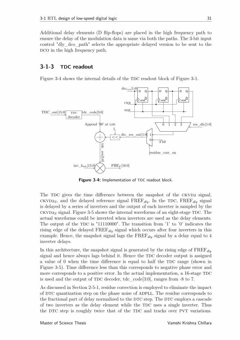
3-1 RTL design of low-speed digital logic 31
Additional delay elements (D flip-flops) are placed in the high frequency path toensure the delay of the modulation data is same via both the paths. The 3-bit inputcontrol "dly_dco_path" selects the appropriate delayed version to be sent to theDCO in the high frequency path.
3-1-3 TDC readout
Figure 3-4 shows the internal details of the TDC readout block of Figure 3-1.
Electronics
tdcdecoder
TDC_out[15:0] tdc_code[3:0]
Append ’00’ at lsb
tdc_res[5:0]
inv_ktdc[15:0] PHEF [16:0]
<<
110
dtc_res_out[1:0]
residue_corr_on
3’b0
0 1 2 3
D Q
Qnrst
D Q
Qnrst
D Q
Qnrst
dtcres[1:0]
res_dly[1:0]
ckr
nrst
Figure 3-4: Implementation of TDC readout block.
The TDC gives the time difference between the snapshot of the ckvd2 signal,ckvd2S, and the delayed reference signal FREFdly. In the TDC, FREFdly signalis delayed by a series of inverters and the output of each inverter is sampled by theckvd2S signal. Figure 3-5 shows the internal waveforms of an eight-stage TDC. Theactual waveforms could be inverted when inverters are used as the delay elements.The output of the TDC is "11110000". The transition from ’1’ to ’0’ indicates therising edge of the delayed FREFdly signal which occurs after four inverters in thisexample. Hence, the snapshot signal lags the FREFdly signal by a delay equal to 4inverter delays.In this architecture, the snapshot signal is generated by the rising edge of FREFdlysignal and hence always lags behind it. Hence the TDC decoder output is assigneda value of 0 when the time difference is equal to half the TDC range (shown inFigure 3-5). Time difference less than this corresponds to negative phase error andmore corresponds to a positive error. In the actual implementation, a 16-stage TDCis used and the output of TDC decoder, tdc_code[3:0], ranges from -8 to 7.As discussed in Section 2-5-1, residue correction is employed to eliminate the impactof DTC quantization step on the phase noise of ADPLL. The residue corresponds tothe fractional part of delay normalized to the DTC step. The DTC employs a cascadeof two inverters as the delay element while the TDC uses a single inverter. Thusthe DTC step is roughly twice that of the TDC and tracks over PVT variations.
Master of Science Thesis Vamshi Krishna Chillara

32 RTL design
CKVD2S
FREFdly0
FREFdly1
FREFdly2
FREFdly3
FREFdly4
FREFdly5
FREFdly6
FREFdly7
TDC range
Figure 3-5: Decoding the output of TDC.
Consequently, the residue is shifted left by 1 place (multiply by 2) and two zeros(corresponding to fractional bits) are appended to the lsb of the "tdc_code" signalbefore they are added together. Moreover, to ensure that both the residue and theTDC output have same delay, a set of three D flip-flops are used to delay the residue.The signal, "res_dly" selects one of these delayed versions. Residue correction canbe turned off by setting the res_corr_on signal to ’0’.Finally, the corrected output of TDC is normalized to the ckvd2 period to obtainthe phase error. This is accomplished by multiplying it by "inv_ktdc" which is theratio of tdc step to ckvd2 period. Since, a fixed relation (2 times) exists betweenthe TDC step and that of DTC, inv_ktdc can be deduced from the value of inv_kdtcwhich is estimated by the kdtc calibration block.
3-1-4 Phase detector
The phase detector implemented in this ADPLL is shown in Figure 3-6. A differencemode architecture is used in which the frequency information is first extracted fromthe phase to generate frequency error which is then accumulated to produce thephase error. The integer part of the variable frequency, dPHVI , is obtained from thedifference of two successive samples of the phase incrementer. It is compared withFCW to obtain the frequency error which is accumulated to produce the integer partof phase error.For the fractional part, a combination of DTC and TDC is used. As discussed inSection 2-5-1, the accumulated value of the fcwfrac is used to generate the dtcctrlas well as the residue that needs to be corrected from the output of TDC. Theoverflow resulting from the accumulation of fcwfrac is added to the integer FCW.The scaling by "inv_kdtc" is required to convert the normalization factor of the delayfrom ckvd2 period to the DTC unit delay. To cover the required range with 1%
Vamshi Krishna Chillara Master of Science Thesis

3-1 RTL design of low-speed digital logic 33
D Q
Qnrstckr
srst
PHVI [6:0]
−
+
FCW[22:16] D Q
Qnrstckr
srst
FCWI1[6:0]
FCW[15:0]D Q
Qnrstckr
srst
FCWaccum[15:0]
FCWaccum[16]
carry-out FCWaccum[15:8] −
+
8’d255 inv_kdtc[8:0]
0
1
dtcctrl1[16:11]
dtcctrl_SPI[5:0]
DTCctrl[5:0]
dtcctrl_extn
dtcctrl1[10:9] DTCresidue[1:0]
+
−
dPHVI [5:0]
dPHRI [6:0]
dPHEI [7:0]D Q
Qnrstckr
dPHEaccum[8:0]
D Q
Qnrst
srst
ckr ZPRA
ZPRP
trst
PHEI [8:0],16’b0
PHEF [16:0]
PHE[22:0]
Figure 3-6: Implementation of phase detector block.
resolution, 6 integer bits and 3 fractional bits are chosen. This value of "inv_kdtc"is obtained from the kdtc calibration block whose basic principle is described inSection 2-5-1. The total phase error is obtained by adding the output of TDC to theinteger part of the phase error.
An additional signal "dtcctrl_extn" is used to facilitate the stand-alone measurementsof DTC. When set to ’1’, the external control to the DTC, dtcctrl_SPI, overrides thecontrol signal generated by the phase detect logic.
Zero-phase restart
The wide tuning range is covered with fine frequency resolution (60 kHz) by dividingthe DCO into three banks: PVT, acquisition, and tracking with increasing resolutionsand decreasing tuning ranges. Only one of the three banks is active at a time andthe inputs to the banks are frozen at their previous values once the DCO mode isswitched. Thus each successive bank operates on the excess phase error left by itsimmediate coarse-bank. Consequently, the phase error that maintains the input tothe coarser bank is not needed as this input is frozen at the instant of mode switch-over. Hence, the accumulator that integrates the frequency error (see Figure 3-6) isreset when the DCO mode is switched from PVT to acquisition or from acquisition totracking. The signals, "ZPRP " and "ZPRA" indicate the mode switchover and resetthe accumulator accordingly. The flip-flop used to delay the integer variable phase,PHVI is reset by a synchronous reset signal which is delayed by 1 ckr period togenerate "trst". This delayed reset signal, trst, resets the accumulator that integratesthe frequency error. This ensures that the accumulator starts to add only after thecorrect frequency error is available, irrespective of the instant at which the phaseincrementer is reset.
Master of Science Thesis Vamshi Krishna Chillara

34 RTL design
3-1-5 Loop filter—PVT bank
Since the three banks of the DCO have different range and resolution, different bitsof the phase error are used to generate their input control words. The tuning wordof the PVT bank depends on the msb bits of the phase error while that of thetracking bank is derived from the lsb bits. Also, since the PVT bank and acquisitionbank are used only for frequency acquisition, the locking time is crucial while thephase noise does not matter during this time. Hence these two banks have justa proportional path resulting in a type-I PLL. Compared to a type-II PLL withan additional integral path, type-I systems lock faster but the DCO phase noiseis suppressed to a lesser extent. A type-II system suppresses the DCO phase noisewith a 40 dB/decade slope whereas a type-I system does so with a 20 dB/decade.Figure 3-7 shows top-level view of the loop filter implemented for each bank. The
Electronics
Phasedetect
PROP
PROP
Gainnorm.
IIRfilter
Gainnorm. CTRL
Gainnorm. CTRL
PROP
INT
CTRL
OTWP
OTWA
OTWT
Loop filterP V T
Loop filterAB
Loop filterT B
Figure 3-7: Loop filter—top level block diagram.
PVT and acquisition banks have a proportional path followed by a normalizationand a control block. The tracking bank has an IIR filter and an integral path inaddition. The gain normalization blocks normalize the DCO control word with theKdco of the corresponding bank to avoid the impact of DCO gain variations on theloop transfer function. The control blocks implement the functionality to generatethe zero-phase restart signals at mode switch-over and also to freeze the tuning wordonce the DCO mode is changed.Figure 3-8 shows the implementation of the proportional, normalization, and controlblocks of the PVT bank. The proportional constant, α, is chosen as a negative powerof 2 as this reduces the hardware complexity by replacing the multiplication by asimple right shift. The number of right shifts can be programmed from 1 to 3 bysetting the value of "alphaP ". The fractional bits of the phase error are neglected asthey do not change the tuning word even with the minimum value of α = 1/23.The DCO gain normalization is done by multiplying the output of proportional pathwith inv_kdco_P = FREF/kdco_P . The value of kdco should be evaluated at halfthe DCO frequency as the loop operates at ckvd2. This normalizes the frequency
Vamshi Krishna Chillara Master of Science Thesis

3-1 RTL design of low-speed digital logic 35
>>
alphaP
PHE[22:16]>>
tempalpha[7:0] 0
1
0
1
phe_d2[7:0]
8’b0
inv_kdco[1]
8’b0
inv_kdco[2]
<<1
inv_kdco[0]
tuneP [4:0]
0
1tuneP [4:0]
D Q
Qnrstckr
nrst
banksel ZPRP
banken
D Q
Qnrstckr
nrst
mem_dcoP [4:0]
OTWP V T [3:0]
OTWP V T [4]reg_dco[4:0]
PROP Gain norm.
CTRL
invisible
Figure 3-8: Loop filter and normalization for PVT bank.
information to reference frequency and decouples the loop transfer function from PVTvariations. Since high accuracy is not required in the PVT bank, this normalizationis implemented by a mantissa multiplier. A series of shifters and adders comprisethe multiplier as shown in Figure 3-8. It implements the following relation:
multiplier =(inv_kdco_P [2] + inv_kdco_P [1]
2)∗ 2inv_kdco_P [0] (3-3)
The LSB of the normalization factor is the exponent while the two MSB formthe mantissa. For typical values of fref = 32 MHz and kdco_P = 21.5/2 MHz,inv_kdco_P is around 3.The control block has the following three functions:
Freeze the PVT input on mode switch-overThe signal banksel, when deasserted, freezes the value of tuning word at reg_dco.It is held permanently until reset or banksel is reasserted.
Generate zero-phase restart signalThe output of the OR gate in the Figure 3-8 is always ’1’ except the instantswhen the value of banksel changes. Thus, a negative pulse of width equal tothe ckr period is generated to indicate the mode switch-over. This negativepulse is used to clear the contents of the phase error accumulator.
Master of Science Thesis Vamshi Krishna Chillara

36 RTL design
Facilitate open-loop testing of the DCOThe signal banken, when zero, sets the value of tuning word calculated by thepreceding blocks to 0. Consequently, the loop has no effect on the control wordof DCO and is effectively open. The DCO can then be tested by varying thevalue of mem_dcoP externally for instance via SPI. mem_dcoP can also beused to start the DCO at a frequency different from the center frequency onreset, thereby reducing the lock time.
Finally, the msb of the tuning word is inverted to convert the signed data intounsigned which then controls the PVT bank of the DCO.
3-1-6 Loop filter—Acquisition bank
To generate the tuning word of acquisition bank, only the msb of the fractionalphase error is used along with 3 integer lsb bits. Before the PLL is locked, the edgeprediction is not accurate and hence the TDC goes out of its narrow range, therebybehaving like a bang-bang phase detector. Hence, only the msb indicating the signof the fractional phase error is used. The proportional, normalization, and controlblocks are similar to those of the PVT bank except for changes in bit lengths (see Fig-ure 3-9). Since the value of "alphaA" is at least 1, it is absorbed into inv_kdco_A toreduce its bit length. The normalization factor is hence FREF/(2*kdco_A), wherekdco_A should be evaluated at half the DCO frequency. The proportional path thenshifts the input phase error right by (alphaA-1).
The multiplication is similar to that of Eq. (3-1-5), except for an additional offsetof 4.
multiplier = 4 +(inv_kdco_A[2] + inv_kdco_A[1]
2)∗ 2inv_kdco_A[0] (3-4)
The control block is also similar and generates the zero-phase restart signal on modeswitch-over, freezes the tuning word at the instant of switch-over, and facilitates theopen-loop testing.
3-1-7 Loop filter—Tracking bank
After the acquisition bank is disabled, the frequency is locked to within one lsb ofthe acquisition bank. The tracking bank then remains active until a new frequencychannel is required. The phase noise of the ADPLL is crucial in this interval and hencea type-II loop filter is used. The control word for the tracing bank is generated bythe 9 msb bits of the fractional phase error. Figure 3-10 shows the implementationdetails of the loop filter, normalization, and control block for the tracking bank.Z-domain analysis of the phase-locked loop (PLL) gives the dependence of loopbandwidth on the proportional constant, α, according to the Eq. (3-5) [32]. Thisassumes that the DCO again is accurately estimated.
BW = α
2πfR (3-5)
Vamshi Krishna Chillara Master of Science Thesis

3-1 RTL design of low-speed digital logic 37
>>
alphaA-1
PHE[22],PHE[18:15]>>
tempalpha[6:0] 0
1
0
1
<<
2
phe_d2[6:0]
8’b0
inv_kdco[1]
8’b0
inv_kdco[2]
<<1
inv_kdco[0]
tuneA[5:0]
0
1tuneA[5:0]
D Q
Qnrstckr
nrst
banksel ZPRA
banken
D Q
Qnrstckr
nrst
mem_dcoA[5:0]
OTWAB [4:0]
OTWAB [5]reg_dco[5:0]
PROP
Gain norm.
CTRL
invisible
Figure 3-9: Loop filter and normalization for acquisition bank.
In this work, α = 2−alphaT and is restricted to negative powers of 2 to simplify thehardware implementation. It can take values from 2−3–2−7. Accordingly, the loopbandwidth can vary from 637 kHz–40 kHz. The value of integral loop constant, ρ,affects the settling behavior of the PLL. The damping factor ζ of the system is givenby:
ζ = 12
(α√ρ
)(3-6)
For an optimum settling behavior, ζ = 1/√
2, and hence ρ should vary from 2−7–2−15.The value of ρ = 2−rho is made programmable and can take only negative powers of2. The integral path can be disabled by setting the signal T2 to zero.Since the lowest value of alphaT is fixed at 3, these 3 right shifts are absorbed intothe value of inv_kdco_T to reduce its bit length. Hence, the value of normalizationfactor is divided by 23 as shown in Eq. (3-7). The alphaT and rho are accordinglysubtracted by three before they shift the input tuning word.
inv_kdco_T = fR8 ∗ kdco_T
(3-7)
An additional IIR filter is used to further suppress the out-of-band phase noise. TheIIR filter implements the following difference equation and the implementation is
Master of Science Thesis Vamshi Krishna Chillara

38 RTL design
PHE[22],PHE[18:7]
inv_kdco[8:0]
>>
>>
tunet[15:0]
lambda[2:0]
+
−
Q D
nrstckrg
nrst
0
1
iiren
ckriiren
ckrg
IIR filter
tuneiir[16:0]
>>
>>
alphat[2:0]-3
rho[3:0]-3
tunerho[16:0]
0
1
D Q
Qnrstckr
nrst
tuneout[14:0]
tuneiir[16 : 0]
T2
tuneout[14:0]
OTW_data[10:0]banksel
banken
D Q
Qnrstckr
nrst mem_dcoT [8:0],5’b0
OTWT B_I [8:0]
OTWT B [9]
OTWT B_F [4:0]
invisible
invisible
Figure 3-10: Loop filter and normalization for tracking bank.
shown in Figure 3-10.y[k] = (1− λ)y[k − 1] + λx[k] (3-8)
where the value of λ = 2−lambda is limited to the negative powers of 2 and determinesthe location of the additional pole that is introduced by the IIR filter according toEq. (3-9).
fP = λ
2πfR (3-9)
As a rule of thumb, this pole is usually set at a frequency ten times to that of thepole introduced by the proportional path. If needed, the IIR filter can be by-passedby setting the signal iiren to 0. The clock is gated with this enable signal to ensurethat the IIR filter does not burn any power when disabled.The two-point modulation requires that DCO gain be estimated and normalizedaccurately. Hence, a full multiplier is used for gain normalization unlike the simplifiedadd and shift structure used for the other two banks. The output of the proportionaland integral path is summed to obtain the control word for the tracking bank.The modulation data, if any, is added to this word to directly modulate the DCO.
Vamshi Krishna Chillara Master of Science Thesis

3-2 System simulation in Verilog 39
Also, banken signal can be set to ’0’ to facilitate open-loop testing similar to theother banks. The tracking bank can then be tuned by changing the external word,mem_dcoT .The msb is inverted to convert the signed word into unsigned and the integer bitsare then sent to the tracking bank of the DCO. The 5 fractional bits are fed to thefirst order Σ∆ modulator to improve the DCO resolution and hence the quantizationnoise as discussed in Section 2-2-2
Σ∆ modulator
A 5-bit first order Σ∆ modulator is used to reduce the quantization noise from theDCO. Figure 3-11 shows its block diagram. A multiplexer selects the dithering clock
D Q
Qnrst
0
1
out[4:0]
OTWT B_F [4:0]
nrst
ckr
ckvd16
clk_sel
out[5]
sigdelen
OTWf
Figure 3-11: First order Σ∆ modulator.
between ckr or ckvd16 depending on the requirements. For instance, in receivemode, good out-of-band phase noise is required and hence a higher dithering ratemay be preferred. The signal clk_sel selects one of these two clocks. The divide-by-2n signals of the DCO output signal are available from the phase incrementer usedto generate variable phase.
3-2 System simulation in Verilog
The high-speed blocks—DCO, divider, and phase incrementer—are modeled behav-iorally in Verilog. Time-domain model of DCO as described in [49] is used for thispurpose. The low-speed blocks requiring custom design i.e., TDC, DTC, and snap-shot circuits are also modeled. These models are used together with the rtl leveldescription of low-speed logic to perform system level simulations in Verilog.Figure 3-12 shows important signals from a Verilog simulation of ADPLL. The signal"bank_sel" changes from ’4’ to ’2’ to ’1’, indicating the transition of ADPLL fromPVT to acquisition to tracking state. The zero-phase restart pulses at each transitioncan also be seen. The frequency of the ADPLL and input controls to each bank arealso shown. The input controls to each bank change only when the correspondingbank is active and are frozen afterwards.
Master of Science Thesis Vamshi Krishna Chillara

40 RTL design
Figure 3-12: System level ADPLL simulation.
Figure 3-13 shows the zoom-in of Figure 3-12 for the PVT state. The PVT bankbrings the output frequency to within one lsb of the PVT bank to the requiredvalue. Figure 3-14 shows the zoom-in of acquisition state and that of tracking stateis shown in Figure 3-15.
Figure 3-13: System level ADPLL simulation—PVT state.
Figure 3-14: System level ADPLL simulation—acquisition state.
Figure 3-15: System level ADPLL simulation—tracking state.
The TDC output code and hence the tracking bank input deviate by large values atthe start of frequency acquisition. This is the result of incorrect phase prediction atthe start which leads to bang-bang operation of the narrow-range TDC. As the outputfrequency becomes closer to the target frequency, the phase prediction becomesaccurate and the TDC operates at its center. Eventually, the output code of TDC
Vamshi Krishna Chillara Master of Science Thesis

3-3 Estimated power consumption 41
oscillates around zero. This is observed in the simulation as shown in Figure 3-15.
3-3 Estimated power consumption
Cadence Encounter is used to synthesize the implemented rtl level low-speed logic.After place and route, the extracted netlist is used along with the activity file gener-ated from the system level simulation to estimate power consumption using SynopsisPrimeTime. The estimated power breakdown of the low-speed digital logic is shownin Table 3-1.
Table 3-1: Estimated power breakdown of the low-speed digital logic.
Block Power consumption (µW)
TX interface 14TDC readout 9FSM 2Phase detector 17Loop filter—PVT 4.5Loop filter—acquisition 5Loop filter—tracking 125Digital loop filter 50Gain normalization 25IIR filter 40
KDTC calibration 35DTC decoder 35
Total 250
Master of Science Thesis Vamshi Krishna Chillara

42 RTL design
Vamshi Krishna Chillara Master of Science Thesis

Chapter 4
Circuit design
In this chapter, the circuit design and physical layout of the analog/high-speedblocks: digitally controlled oscillator (DCO), DCO buffer, divider, and phase incre-menter, are described with a focus on lowering the overall power consumption.
4-1 Digitally controlled oscillator (DCO)
As discussed in Section 2-1-1, a DCO is at the heart of an all-digital phase-lockedloop (ADPLL). It takes a digital input control word called the oscillator tuningword (OTW) and generates a sinusoidal output with a frequency proportional toOTW plus an offset. The performance of the frequency synthesizer—area, power,and spectral purity—depends to a large extent on that of the DCO. Hence consid-erable effort is put into its design, which is discussed in this section. The generaldesign considerations, namely power, phase noise, and tuning range, are first dis-cussed followed by a description of its building blocks —inductor, active part, andcapacitor bank. The physical layout, which affects the overall performance is alsodiscussed and the simulation results with post-layout parasitics are presented.An LC tank based oscillator with a fixed inductor and digitally tunable capacitorbanks is used to realize the DCO. The oscillation occurs at the resonance frequencyof the LC tank. A positive-feedback or a negative resistance is used to compensatethe energy-loss resulting from the parasitics in the LC tank, thereby sustaining theoscillation. The frequency tuning can be achieved either by changing the inductoror the capacitor. However, it is easier to change the capacitor rather than an induc-tor in monolithic implementations. Moreover, adding switches to the inductor willfurther degrade the already low quality factor of the on-chip inductors. Hence, alarge number of capacitor cells controlled by the OTW is used to achieve the digitalcontrol of the oscillator frequency. The frequency of the DCO with N capacitor cellsand an inductance L is given by Eq. (4-1).
f = 1
2π
√√√√L ∗ N−1∑i=0
Ck
(4-1)
Master of Science Thesis 43 Vamshi Krishna Chillara

44 Circuit design
In this work, a DCO covering a frequency range of 2.4–2.7 GHz with a phase noiseof -110 dBc/Hz at 1 MHz offset from the oscillating frequency and a raw frequencyresolution of 60 kHz is targeted. The design goal is to achieve this phase noiseperformance over the required tuning range with minimum power consumption. Thedesign variables are the choice of inductor and capacitor values, width and lengthof the transistors in the active part and bias current.
4-1-1 Inductor
The power dissipated in the LC tank needs to be replenished so as to sustain theoscillation, which places a lower limit on the power consumption of the DCO. Thisloss power can be calculated by a simple tank model as shown in Figure 4-1. In
L Rs
C
−R
Figure 4-1: RLC model of the LC tank.
the figure, the losses in the inductor due to the finite resistance of the metal isrepresented as a series resistance Rs. The quality factor of the on-chip inductors isusually worse than that of the capacitor banks and hence they dominate the overallenergy loss of the LC tank. Hence, the capacitor losses are neglected. The negativeresistance is used to model the active element that compensates the LC tank loss.The maximum energy stored in the inductor and capacitor is equal and is given byEq. (4-2).
Emax = 12LI
2peak = 1
2CV2peak (4-2)
where, Vpeak and Ipeak represent the peak values of the voltage across the LC tankand current through it. The current Ipeak flows through Rs resulting in a power lossequal to
Ploss = 12I
2peakRs = 1
2CV 2
peakRs
L(4-3)
The operating frequency is usually fixed and hence Eq. (4-3) can be rewritten as
Ploss = 12V 2peakRs
L2ω2 = 12V 2peak
LωQL
(4-4)
where QL is the quality factor of the inductor defined as the ratio of the imaginarypart of the impedance to the real part as shown in Eq. (4-5).
QL = ωL
R(4-5)
Vamshi Krishna Chillara Master of Science Thesis

4-1 Digitally controlled oscillator (DCO) 45
From Eq. (4-4) it is clear that for a given loss resistance and operating frequency ofthe oscillator, the larger the inductance the lower is the power consumption. Also,decreasing the series resistance or increasing the quality factor of the inductancelowers the power consumption.The largest value of the inductor that can be chosen is usually limited by the re-quirement on tuning range or the area. For a given operating frequency, a largevalue of inductance results in a small value of capacitance, limiting the tuning rangethat can be achieved. Moreover, a large inductor is accompanied by a large couplingcapacitance to the substrate, thereby decreasing the self-resonant frequency. Beyondthis self-resonant frequency, the coil can no longer be used as an inductor thus im-posing an upper limit on the achievable inductance value at a certain frequency instandard CMOS process. Also, it should be noted that the larger the inductancethe bigger is the frequency step for a fixed capacitance step. On the other hand, thequality factor is limited by the technology (thickness and conductivity of availablemetal layers).Finding the optimum value of inductance, which is just enough to satisfy the tuningrange with a reasonably large self-resonant frequency is non-trivial. After estimatingthe amount of fixed parasitic capacitance from the capacitor banks and active part,a value of 7.7 nH is chosen after some iterations. The inductance available from theTSMC library is used in this work. The inductance with top most metal layers—which are the thickest and hence have lowest resistivity—is chosen to maximize thequality factor. Moreover, it results in lower coupling capacitance as it is farthestfrom the substrate.Figure 4-2 shows the plot of the inductance as a function of frequency across typical,fast, and slow corners. The self-resonance frequency—beyond which an inductor
FF: 2.4G 7.240657n
TT: 2.4G 7.751025n
SS: 2.4G 8.272301n
Inductance (n)
-25.0
-9.0
7.0
23.0
39.0
55.0
Frequency (G)0.0 2.0 4.0 6.0 8.0
Figure 4-2: Inductance vs frequency across process corners.
behaves like a capacitor—is sufficiently far (>6 GHz) from the required operatingfrequencies (2.4–2.7 GHz). The value of inductance varies by almost 1 nH amongdifferent corners. This corresponds to a frequency deviation of nearly 150 MHz at
Master of Science Thesis Vamshi Krishna Chillara

46 Circuit design
2.4 GHz. To ensure DCO supports the required tuning range across process variations,a margin of 150 MHz on either side is added to its tuning range.
TT: 2.4G 14.16071
SS: 2.4G 12.74497
FF: 2.4G 15.84502
17.0Quality factor
3.4
6.8
0.0
10.2
13.6
Frequency (G)0.0 2.0 4.0 6.0 8.0
Figure 4-3: Q-factor vs frequency across process corners.
Figure 4-3 shows the plot of the quality factor of the inductance with frequencyacross process corners. The quality factor is around 14 in the typical case with a10% variation across corners.
4-1-2 Active part and biasing
A complementary cross-coupled topology is used to provide the negative resistancein the circuit of Figure 4-1, which replenishes the tank losses. Compared to thestructure with just an NMOS or a PMOS, complementary structure reuses the biascurrent, thereby providing roughly twice the transconductance for the same current.It provides a negative resistance of
R = −2/(gm,n + gm,p) (4-6)
where gm,n and gm,p denote the transconductance of NMOS and PMOS transistorsrespectively.Figure 4-4 shows the circuit schematic of the implemented DCO. Instead of a MOScurrent source, a poly-silicon resistor is used for biasing the DCO [50]. The currentsource is usually the dominating source of phase noise by means of flicker-noise up-conversion. Using a resistor avoids this and the thermal noise associated with it isfiltered by means of a tail capacitor, Ctail.The bias current is controlled by 5 parallel resistors connected to the supply rail byPMOS switches. A binary 5-bit digital word controls these switches, and hence thebias current. In addition, another resistor in parallel is always turned on providinga minimum offset current. The DCO current can vary from 80 µA to 450 µA at 1 Vsupply. The bias control can be used to implement swing voltage regulation in futuredesigns to ensure optimum current consumption over the entire frequency range.
Vamshi Krishna Chillara Master of Science Thesis

4-1 Digitally controlled oscillator (DCO) 47
7.7nH
Coarse
Medium
Fine
VDD
Bias Control
5
6
9
5
Ctail
Figure 4-4: Circuit schematic of the implemented DCO.
The length of the transistors in the cross-coupled pair is chosen at 100 nm (minimumlength: 40 nm) to minimize the flicker noise. The width of the transistors is increaseduntil the gm is sufficient to sustain the oscillation. The PMOS transistors are madethrice as wide as the NMOS devices to account for lower hole mobility. Using alarge aspect ratio pushes the transistors into weak-inversion region offering a bettergm–Id efficiency. However, it also increases the capacitance contribution from theactive part to the tank, limiting the achievable tuning range. Moreover, since thiscapacitance comprises junction capacitance, it depends non-linearly on the nodevoltage, making the oscillator susceptible to supply pushing.Figure 4-5 shows the layout of the active part of the DCO. The fingers of the cross-coupled pair are arranged in a common-centroid configuration to average out thelinear process variations. Also, the transistors are laid out to have same orientationfor better matching. The layout is made compact to minimize the routing parasiticsat the drain terminal of the cross-coupled pair as they are absorbed into the LCtank, reducing the maximum frequency attainable.
4-1-3 Capacitor banks
Design of capacitor banks is challenging in that they need to be tunable over a largefrequency range with a fine step. A tuning range of 2.25 GHz to 2.85 GHz witha 60 kHz step is targeted to leave enough margin for process variations to cover
Master of Science Thesis Vamshi Krishna Chillara

48 Circuit design
Cross-coupled
pair
Switchable
resistors
Ctail
To inductor
To inductor
Figure 4-5: Layout of the active part of the DCO.
the required 2.4 GHz to 2.7 GHz range. This results in a resolution requirement ofnearly 14 bits, which is difficult to achieve even with advanced component matchingtechniques. Generally, a 9-bit resolution is possible without resorting to matchingtechniques or digital calibration [32]. Fortunately, the fine 60 kHz resolution needsto cover a frequency deviation of at most 2 MHz corresponding to the frequencydeviation required by the direct frequency modulation. Thus, a segmented approachcan be used where three banks—coarse, medium, and fine—cover the desired tuningrange with required resolution. The coarse, medium, and fine banks are referred toas PVT, acquisition, and tracking banks following the nomenclature used in [32].The PVT bank covers the whole tuning range with very coarse resolution. The ac-quisition bank then brings the output frequency closer to the required channel fre-quency. The PVT and acquisition banks are active only at the start of the frequencyacquisition as discussed in Section 3-1-1. Finally, the tracking bank locks to thetarget frequency channel with a fine resolution and needs to cover a range equal toeither the step of medium bank or the modulation range, whichever is larger. Ontop of this, it should have sufficient margin to correct the frequency drifts in theoscillator over time.The range and resolution of each bank is determined as follows. The range of thePVT bank is made equal to the required tuning range. The resolution of the trackingbank is determined by the required frequency resolution according to Eq. (4-7)
∆f = (2π2Lf 3)∆C (4-7)
Vamshi Krishna Chillara Master of Science Thesis

4-1 Digitally controlled oscillator (DCO) 49
A 60 kHz resolution corresponds to a frequency step of roughly 20 aF at 2.7 GHzoutput and 7.7 nH inductance. To have sufficient overlap between two consecutivecapacitor banks, a ratio of 7–8 is chosen between the step of the coarser bank tothe range of its immediate fine bank. Using these criteria, a 9-bit tracking bit witha 60 kHz step, 6-bit acquisition bank with a 2.5 MHz step, and a 5-bit PVT bankwith a 20 MHz step are chosen.Another important requirement of the capacitor banks is their quality factor. Thetotal tank quality factor is given by the mathematical parallel combination of theinductor and capacitor quality factors. Hence, quality factor of the capacitor banksshould be made large compared to that of the inductor so that overall Q is limitedby that of the on-chip inductance. As mentioned earlier, a Q of 15 is achievable foron-chip inductors in the TSMC 40 nm technology. Hence, a quality factor of 50 istargeted for the capacitor banks in both ON and OFF states.
PVT bank
The PVT bank determines the tuning range of the DCO. A capacitor bank witha large frequency range, i.e., large
(Cmax
Cmin
)ratio is desired as it minimizes the off-
state capacitance. This in-turn allows the use of a larger inductance and henceresults in lower power consumption as discussed in Section 4-1-1. A switched MOMconfiguration shown in Figure 4-6 is used a unit cell of the PVT bank as it canprovide high tuning range. When the switch is enabled, the series combination of
P
CMOM CMOM
N
EN
Figure 4-6: Switched MOM configuration.
two MOM capacitors, CMOM/2, appears across the terminals P and N and the unitcell is considered to be in ON state. On the other hand, when the switch is open,the capacitance that appears across P and N is determined by the parasitics of theswitch and the MOM capacitors.Quality factorIn the ON state, the switch of Figure 4-6 can be replaced by a resistance RON ofthe transistor used to implement the switch. The impedance across P and N is thengiven by Z = RON + 1
jω
(CMOM
2
) giving rise to an on-state quality factor of
Qon = 1ωRon
(CMOM
2
) (4-8)
It is clear that Ron of the switch should be made as small as possible to have a goodQ. Hence an NMOS is used instead of PMOS as the mobility and hence conductanceof the electrons is 2–3 times that of holes. The ON resistance of a MOS switch canbe expressed as
Ron = 1µncox
WL
(vgs − vth)(4-9)
Master of Science Thesis Vamshi Krishna Chillara

50 Circuit design
Eq. (4-9) indicates that the aspect ratio(WL
)and the overdrive voltage (vgs − vth)
should be maximized to reduce the on resistance. However, increasing the aspectratio also increases the parasitic capacitance of the MOS switch and hence theoff-state capacitance, thereby degrading the capacitance range. To maximize theoverdrive voltage, two pull-down NMOS transistors are used to pull the DC voltageof source and drain terminals of the MOS switch to ground in ON state. The aspectratio of the MOS switch is then increased until its Qon reaches 50.
In the off-state the parasitic capacitance between drain and source terminals of theswitch appears between the two MOM capacitors leading to an off-state capacitanceof
Coff = CMOMCparCMOM + 2Cpar
(4-10)
which is nearly equal to the value of parasitic capacitance. The capacitance has thefollowing contributions: drain and source junction capacitors of the NMOS switch,drain junction capacitance of the pull-down transistors, and the parasitics from theMOM capacitor to substrate. The quality-factor in the off-state is largely determinedby that of the MOM capacitors which is quite high.
The DC-voltage at the drain and source terminals of the NMOS switch is set by theleakage current through the pull-down transistors which are now turned-off. Sincethe DCO output swing is typically around 300 mV – 400 mV, the maximum negativevoltage at the source terminal of the NMOS switch is around 200 mV. Hence, thegate-to-source voltage of the NMOS switch is always less than its threshold voltage,ensuring the switch remains off.
Figure 4-7 shows the circuit implementation of the unit cell of the PVT bank. An
C
Enb Enb
EnbC
EnbEn
Figure 4-7: Circuit schematic of the unit cell of PVT bank.
inverter is placed between the input control and the switch-enable so that capaci-tance is lowest when the bank is turned on. This results in a positive kdco, i.e., thefrequency increases with increasing input control.
The 5-bit PVT bank is binary weighted and the cells corresponding to the higherorder bits are made from multiple unit cells. The cell corresponding to bit 1 comprises21 unit cells and bit 2 comprises 22 unit cells and so on. This ensures that thecapacitance decreases monotonically with the input control. Also, the linearity isimproved as systematic mismatches are reduced.
Vamshi Krishna Chillara Master of Science Thesis

4-1 Digitally controlled oscillator (DCO) 51
Figure 4-8 shows the physical layout of the 5-bit PVT bank. The unit cells areplaced in a 4x8 matrix with 1 dummy cell. The cells are laid out such that theyhave a common centroid to suppress the mismatches resulting from linear gradientsacross the die. The layout parasitics are extracted using Calibre and the post-layout
60 µm
40 µ
m
Unit cell
CMOM
CMOM
switch
Figure 4-8: Layout of the PVT bank.
simulations to estimate the Q-factor and capacitance range are done using CadenceSpectre. The capacitance and Q-factor are calculated from the input impedance ofthe bank. Figure B-1 shows the C–V curve of the unit cell of the PVT bank.The capacitance step is 8.8 fF with an off-state capacitance of 4.5 fF. The qualityfactor in ON and OFF states is shown in Figure B-2. As can be seen, the qualityfactor is limited in the ON-state and is 48, sufficiently higher than that of theinductor. Figure 4-9 shows the total capacitance range of the PVT bank includingthe routing parasitics. The PVT bank has a minimum capacitance step of 140 fF andcovers a capacitance range of 273 fF with a 8.8 fF step.
31.0 140.75192fA
0.0 413.70769fA
Capacitance total (fA)
100.0
150.0
200.0
250.0
300.0
350.0
400.0
450.0
OTW_PVT[4:0]0.0 5.0 10.0 15.0 20.0 25.0 30.0 35.0
dx: 31.0
dy: 272.95577fA
s: 8.8050249fA/
Figure 4-9: Capacitance range of the PVT bank.
Master of Science Thesis Vamshi Krishna Chillara

52 Circuit design
Acquisition bank
The acquisition bank is implemented in a similar way as the PVT bank with smallerMOM capacitors. From Eq. (4-8), it can be seen that the on-state Q-factor increaseswhen CMOM decreases. Consequently, smaller switches are sufficient to achieve therequired quality factor, resulting in a lower off-state capacitance. The 6-bit acquisi-tion bank is realized from 63 unit cells controlled in a binary manner. The layoutof the bank is shown in Figure 4-10. The unit cells are arranged in a matrix of 8x8while ensuring a common-centroid. The acquisition bank occupies lesser area thanPVT bank due to the lower CMOM used. The post-layout simulations are performed
65 µm
30 µ
m
Unit cell
Figure 4-10: Layout of the acquisition bank.
to estimate the value of capacitance step, quality factor and capacitance range, andare shown in Figure B-3 and Figure B-4 respectively. The capacitance step of theunit cell is 1.2 fF with an off-state capacitance of 0.7 fF. The quality factor is greaterthan 50 in both ON and OFF states. Note that due to the presence of the inverterat the input of the switch, the ON state corresponds to low enable voltage in thesimulation plots.
The total capacitance of the acquisition bank as a function of its 6-bit input con-trol word is shown in Figure 4-11. The capacitance decreases monotonically withOTW_AB[5:0]. The minimum capacitance from the acquisition bank is only 44 fF,thanks to the smaller dimensions of the NMOS switch. The 6-bit acquisition bankhas a tuning range of 76 fF.
Vamshi Krishna Chillara Master of Science Thesis

4-1 Digitally controlled oscillator (DCO) 53
0.0 121.13476fA
63.0 44.891721fA
Capacitance total (fA)
40.0
60.0
80.0
100.0
120.0
OTW_AB[5:0]0.0 10.0 20.0 30.0 40.0 50.0 60.0 70.0
dx: 63.0
dy: 76.243042fA
s: 1.210207fA/
Figure 4-11: Capacitance range of the acquisition bank.
Tracking bank
Tracking bank locks the PLL frequency to the target frequency with the requiredresolution. The frequency resolution of this bank determines the resolution of theDCO. To achieve a 60 kHz resolution, a 20 aF capacitance is required as given byEq. (4-7). The MOS varactors in an accumulation mode or depletion mode arethe common choices to achieve this fine resolution [17, 51]. However, this requiresaccurate models for the varactor mode operation of the MOS transistor. Also, theC-V transfer curve of the MOS varactor is susceptible to PVT variations. Hence,fine bank is also realized using MOM capacitors which are better modeled and lessprone to PVT variations.
The circuit implementation of the unit cell of the tracking bank is shown in Figure 4-12 [52]. When the control signal is high, the input to the NMOS switch is low and
CsCs
Cb Cb
Enb
Enb
Enb
EnbEn
Figure 4-12: Circuit schematic of the unit cell of tracking bank.
is hence turned off. The capacitance in this state is given by the series combination
Master of Science Thesis Vamshi Krishna Chillara
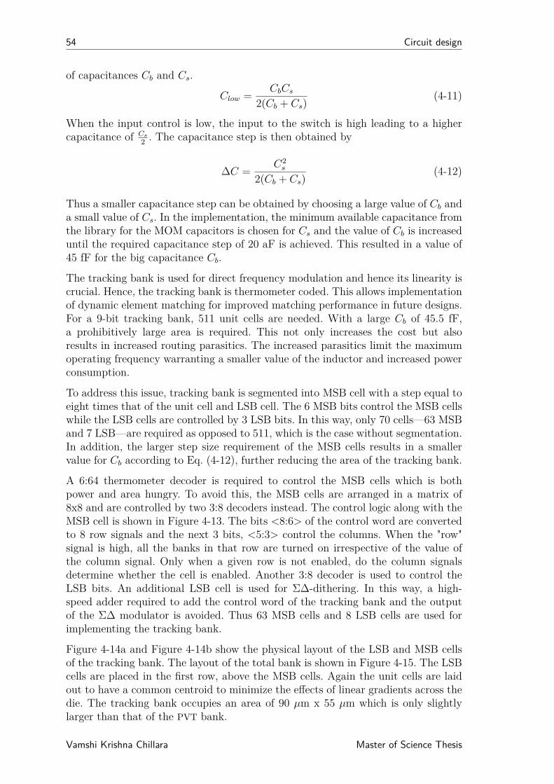
54 Circuit design
of capacitances Cb and Cs.
Clow = CbCs2(Cb + Cs)
(4-11)
When the input control is low, the input to the switch is high leading to a highercapacitance of Cs
2 . The capacitance step is then obtained by
∆C = C2s
2(Cb + Cs)(4-12)
Thus a smaller capacitance step can be obtained by choosing a large value of Cb anda small value of Cs. In the implementation, the minimum available capacitance fromthe library for the MOM capacitors is chosen for Cs and the value of Cb is increaseduntil the required capacitance step of 20 aF is achieved. This resulted in a value of45 fF for the big capacitance Cb.
The tracking bank is used for direct frequency modulation and hence its linearity iscrucial. Hence, the tracking bank is thermometer coded. This allows implementationof dynamic element matching for improved matching performance in future designs.For a 9-bit tracking bank, 511 unit cells are needed. With a large Cb of 45.5 fF,a prohibitively large area is required. This not only increases the cost but alsoresults in increased routing parasitics. The increased parasitics limit the maximumoperating frequency warranting a smaller value of the inductor and increased powerconsumption.
To address this issue, tracking bank is segmented into MSB cell with a step equal toeight times that of the unit cell and LSB cell. The 6 MSB bits control the MSB cellswhile the LSB cells are controlled by 3 LSB bits. In this way, only 70 cells—63 MSBand 7 LSB—are required as opposed to 511, which is the case without segmentation.In addition, the larger step size requirement of the MSB cells results in a smallervalue for Cb according to Eq. (4-12), further reducing the area of the tracking bank.
A 6:64 thermometer decoder is required to control the MSB cells which is bothpower and area hungry. To avoid this, the MSB cells are arranged in a matrix of8x8 and are controlled by two 3:8 decoders instead. The control logic along with theMSB cell is shown in Figure 4-13. The bits <8:6> of the control word are convertedto 8 row signals and the next 3 bits, <5:3> control the columns. When the "row"signal is high, all the banks in that row are turned on irrespective of the value ofthe column signal. Only when a given row is not enabled, do the column signalsdetermine whether the cell is enabled. Another 3:8 decoder is used to control theLSB bits. An additional LSB cell is used for Σ∆-dithering. In this way, a high-speed adder required to add the control word of the tracking bank and the outputof the Σ∆ modulator is avoided. Thus 63 MSB cells and 8 LSB cells are used forimplementing the tracking bank.
Figure 4-14a and Figure 4-14b show the physical layout of the LSB and MSB cellsof the tracking bank. The layout of the total bank is shown in Figure 4-15. The LSBcells are placed in the first row, above the MSB cells. Again the unit cells are laidout to have a common centroid to minimize the effects of linear gradients across thedie. The tracking bank occupies an area of 90 µm x 55 µm which is only slightlylarger than that of the PVT bank.
Vamshi Krishna Chillara Master of Science Thesis

4-1 Digitally controlled oscillator (DCO) 55
CsCs
Cb Cb
Enb
Enb
Enb
Enb
RWLS
CL
RW
Figure 4-13: Circuit schematic of the MSB cell of tracking bank.
Cb Cb
Cs Cs
(a) LSB cell
CbCb
CsCs
(b) MSB cell
Figure 4-14: Physical layout of the unit cell of tracking bank
The post-layout estimations of the capacitance step and quality factor of MSB celland LSB cell are shown in Figure B-7 and Figure B-8; and Figure B-5 and Figure B-6, respectively. The quality factor of both banks is greater than 50 in ON and OFFstates. The LSB cell has a step of 18 aF and the MSB cell has a step of 145 fF whichis approximately eight times the LSB step.Figure 4-16 shows the capacitance of the tracking bank as a function of its 9-bitcontrol word. The tracking bank has significant constant minimum capacitance of73 fF. It covers a range of 9 fF with an average step of 18 aF.The operating range and design of the quality factors of the three capacitor banksis summarized in Table 4-1. The total off-state capacitance from all three banks isaround 260 fF.
Master of Science Thesis Vamshi Krishna Chillara

56 Circuit design
90 µm
55
µm
LSB cell
MSB cells
MSB unit
Figure 4-15: Physical layout of the tracking bank.
Table 4-1: Summary of capacitor banks.
Bank type Bits Cmin Range ∆C Qmin
(fF) (fF)PVT 5 140.7 273 8.8 fF 48
Acquisition 6 45 76.2 1.2 fF 58Tracking 9 73 9.5 18 aF 66segmented (6+3)
511.0 73.004489fA
0.0 82.472575fA
Capacitance total (fA)
72.5
75.0
77.5
80.0
82.5
OTW_TB[8:0]0.0 106.0 212.0 318.0 424.0 530.0
dx: 511.0
dy: 9.4680866fA
s: 18.528545aA/
Figure 4-16: Capacitance range of the tracking bank.
Vamshi Krishna Chillara Master of Science Thesis

4-1 Digitally controlled oscillator (DCO) 57
4-1-4 Layout
The physical layout of the individual banks and the active part have already beenpresented. These blocks are arranged to minimize the routing parasitics from theinductor to capacitor banks and the active part as shown in Figure 4-17. Long
285 µm
31
0 µ
m
150 µm
11
0 µ
m
TB AB PVT
Active part
Figure 4-17: Layout of the DCO.
metal lines not only increase the fixed capacitance of the tank but also decrease thequality factor by increasing the series resistance. Top metals with large width areused for connecting the inductor with rest of the DCO to minimize the quality factordegradation. The capacitor banks and the active part are placed symmetrically aboutthe inductor.
Post-layout simulations
The parasitics from the layout are extracted using Calibre and the post-layout sim-ulations are performed to estimate the current consumption, swing, and phase-noiseof the DCO. The effect of bond wire connections from supply to the chip are modeledby a 2 nH inductor. The capacitor banks are modeled using Verilog-A by using thecapacitance step, range, and quality factor obtained from separate post-layout sim-ulations. The rest of the DCO is simulated using the Calibre extracted views. Thisspeeds-up the simulation significantly without sacrificing the accuracy.Figure 4-18 shows the output of the DCO obtained from the transient simulation.The single-ended output swing is around 335 mV for a current consumption of148 µA. The common-mode voltage is around 370 mV and is also shown in thefigure. Figure 4-19 shows the phase-noise of the DCO estimated using the periodicsteady-state (PSS) analysis. A phase-noise of -113 dBc/Hz at 1 MHz offset from theoperating frequency is achieved. The major noise contributors are the inductanceand the cross-coupled pair. The current consumption can be traded for phase-noiseusing the 5-bit bias control word.
Master of Science Thesis Vamshi Krishna Chillara

58 Circuit design
Figure 4-18: Transient simulation of the DCO.
Figure 4-19: Phase-noise simulation of the DCO.
Vamshi Krishna Chillara Master of Science Thesis

4-2 DCO buffer 59
4-2 DCO buffer
The DCO needs to drive the PA and divide-by-2 pre-scaler as shown in Figure 2-5. Abuffer is typically used to isolate the DCO from the effects of varying load, referredas load-pulling. Also, it allows the DCO to operate in the current-limited regime witha low output swing to reduce the power consumption. The implementation of thisDCO buffer is discussed in this section.
4-2-1 Self-biased inverter
Since inverter based buffers are power efficient, a self-biased inverter, shown in Fig-ure 4-20, is typically used as the DCO buffer. The DC-level of the DCO output is
Rbias
Cbias
From oscillator To PA and divider
Figure 4-20: Self-biased inverter as the DCO buffer.
prone to PVT variations. Consequently, the output of the oscillator is ac-coupled tothe buffer by means of a large coupling capacitor. Thus, the variations on the DC-level of the oscillator output do not impact the buffer output. The DC-level at theinput of the buffer is fixed by a large resistor Rbias. Since the resistor is connected tothe gate of the NMOS and PMOS of the inverter, no DC voltage drop occurs acrossit. This results in a same DC-voltage at the input and output nodes of the inverteri.e., it lies on the line "Vin = Vout". As shown in the Figure 4-21, the DC-level of
Vin
Vout
VTC
Vbias
Figure 4-21: Biasing the self-biased inverter.
the signal is the point of intersection of the VTC and Vin = Vout curves. The VTC
Master of Science Thesis Vamshi Krishna Chillara

60 Circuit design
of the inverter is fixed such that this point of intersection corresponds to the pointof maximum sensitivity on the voltage transfer characteristic (VTC) of the inverterand hence enables operation with low input-swing.
However, this approach uses passive components—Cbias and Rbias—that do not scalewith technology. Hence it occupies a large area leading to higher system costs. More-over, the large resistor Rbias used for biasing is a source of significant thermal noisewhich couples into the oscillator output, thereby degrading the phase noise perfor-mance. Thus the oscillator needs to expend more current to maintain the requiredphase noise levels. Furthermore, the large decoupling capacitor introduces signifi-cant parasitics, thereby loading the output node of the oscillator. This increases thepower consumption as well as reduces the maximum operable frequency of the os-cillator. Thus a self-biased inverter based buffer poses a serious challenge in scalingdown the power consumption.
4-2-2 DC coupled buffer with tunable VTC
To address the aforementioned problems of self-biased inverter, a DC-coupled bufferwith tunable VTC is proposed. In this approach, the bulky passives are avoided byDC coupling the oscillator output to the buffer. The variation in the DC-level ofthe DCO output now affects the operation of the buffer. Thus, to ensure the DCObuffer always operates at its maximum sensitivity point, VTC of the inverter is tunedas shown in Figure 4-22. In this way, the DC-level of the oscillator output alwayscorresponds to the maximum sensitivity point on the VTC of the buffer.
To summarize, in an ac-coupled self-biased inverter (Figure 4-20), the VTC is fixedat its optimum point, such that the input DC-level set by Rbias ensures operation atmaximum sensitivity. On the other hand, in the presented approach, the DC-level ofthe input buffer is fixed (by the DC-level of DCO output), while the VTC is changedto ensure the operation at maximum sensitivity point across PVT variations. In thisway, an area efficient low-power buffer which operates with low-input swing overPVT variations is realized.
Figure 4-22 illustrates the idea of tuning the VTC for operation across process vari-ations. The VTC of the inverter is varied by digitally controlling the device ratio of
Vin
Vout
Tunable VTC
wp/wn
Vbias
Figure 4-22: Tuning the VTC of the inverter.
Vamshi Krishna Chillara Master of Science Thesis

4-2 DCO buffer 61
PMOS to NMOS (wp/wn) of the inverter to cover process variation.Figure 4-23 shows the schematic of the proposed buffer with digitally tunable VTC.The variation in DC-level of the oscillator output is estimated from Spectre simula-tions across process corners. The number and width of the switchable PMOS/NMOSdevices is then chosen to cover this variation with extra margin. Four PMOS andNMOS devices with binary weighted widths serve as the additional devices and arecontrolled by the 5-bit digital word.When the input code is "00000" i.e., none of the additional devices are connected, adefault PMOS-NMOS pair is connected. This pair is sized to drive the subsequentload while operating at the maximum sensitivity point for an input DC-level cor-responding to the typical corner. The MSB of the 5-bit buffer control determineswhether PMOS or NMOS are turned on while the 4 LSB bits determine the numberof those devices that are turned on.
In
Out
EnP
EnN
WP
WN
out1
VDD
Figure 4-23: Schematic of the proposed VTC-tunable buffer.
The subsequent buffer of Figure 4-23 is used to drive the large output load. In itsabsence, the default pair of the tunable-buffer should be very large. This, in turnwarrants large sizes for additional devices to alter the wp/wn ratio significantly,leading to a larger overall size of the buffer. Thus, the first buffer brings the low-input swing to rail-to-rail level and drives the relatively small subsequent bufferwhich drives the actual load (PA and divider).By monitoring the duty-cycle of the oscillator output signal, the control code thattunes the VTC to the desired position is generated. At the optimal biasing point,the duty cycle of the oscillator output is 50%. If the input bias level is larger thanthe optimum level, then the digital control enables more PMOS devices such thatthe VTC shifts to the right. Similarly, if the input bias is smaller than the optimalpoint, more NMOS devices are enabled to shift the VTC towards left.From post-layout simulations across various process corners, variation of the DC-level of the DCO output signal is estimated. At 1 V supply, the DC-level varies from330 mV to 400 mV. The buffer is then designed to cover this range by adding NMOSand PMOS devices in parallel to the first inverter. These are connected to GND and
Master of Science Thesis Vamshi Krishna Chillara

62 Circuit design
VDD lines via switches which are controlled by the 5-bit buffer control word. TheMSB of the control word decides if additional PMOS or NMOS devices are requiredwhile the 4 LSB bits determine the number of devices connected in parallel to thefirst stage.
Figure 4-24 shows the transient simulation of the buffer across various process cor-ners. By setting an appropriate control word, the buffer can withstand the DC-levelvariations on its input signal. The phase noise simulation from PSS analysis is alsoshown. The buffer consumes 56 µA and has a phase noise of -123 dBc/Hz at 1 MHzoffset which 10 dB lower than that of the DCO.
Figure 4-24: Operation of the buffer across process corners and phase-noise.
Since the proposed structure avoids passive components, it occupies a very smallarea of 5 µm x 10 µm and is aligned with the technology scaling. In comparison,a self-biased inverter would need a coupling capacitor of the order of 0.5 pF and abiasing resistor of the order of 200 kΩ. The coupling capacitance should be largeenough to not attenuate the sinusoidal output of the DCO and the value of 0.5 pFis obtained from Spectre simulations. Using crtmom capacitor and ppoly resistorsfrom TSMC library, the area of these two is estimated at 20 µm x 20 µm or eighttimes that of the DC-coupled buffer. Moreover, the power consumption is reducedby avoiding driving the bulky parasitics associated with the decoupling capacitors.Also, noise feed-through from the bias resistor is absent, thereby allowing lowercurrent consumption for a given phase noise requirement compared to the traditionalapproach.
Vamshi Krishna Chillara Master of Science Thesis

4-3 Divider 63
4-3 Divider
As discussed in Section 2-1, a divide-by-2 block is used after the DCO buffer andthe divided down output clock is used for phase detection. This helps in reducingthe operating frequency of the phase incrementer and hence saves power. A sense-amplifier based divider [5] is ideal when the low-input swing operation is needed. Inthis work, since the DCO buffer boosts the output to rail-to-rail voltage, a dynamicCMOS divider is used for its high-speed, low-power operation. The dynamic dividersare fast since they avoid the positive feedback transistors required to store the outputuntil the next significant edge of the clock. Instead, the device and routing parasiticcapacitances are used for storing the value. Since the operation frequency is quitehigh, the nodes are refreshed before the capacitor discharges, thereby retaining thevalue. Transmission gate based and tri-state inverter based dividers are comparedto chose the optimum architecture.
4-3-1 Transmission-gate based dynamic divider
A transmission-gate based dynamic CMOS divider is shown in Figure 4-25 [53].
CKV
CKV
CKV
CKV
CKV
CKV
CKV
CKV
rst rst
nrst nrst
nrst rst
I+ Q+
Q-I-
VDD VDD
Figure 4-25: Transmission-gate based dynamic CMOS divider.
The transmission-gate inverter combination acts as a simple D-latch, with para-sitics at the output of transmission gate acting as the storage element. The cascadeof two-latches forms a master-slave flip-flop. Two such D-flip flops are cross-coupledto obtain a divider-by-2 with quadrature output phases. The outputs of each trans-mission gate should be initialized properly for this configuration to provide the re-quired divide-by-2 signals. This is accomplished by the pull-up and pull-down MOStransistors which are activated only at the reset.
Master of Science Thesis Vamshi Krishna Chillara

64 Circuit design
4-3-2 Tri-state inverter based dynamic divider
Figure 4-26 shows the simplified circuit schematic of the tri-state inverter baseddynamic divider. A tri-state inverter replaces the transmission-gate inverter combi-
rst rst
nrst rst
CKV
CKV
CKV
CKV
CKV
CKV
CKV
CKV
nrst nrst
Tri-state inverter
I+ Q+
Q-I-
VDD VDD
VDD
Figure 4-26: Tri-state inverter based dynamic CMOS divider.
nation of the previous configuration (see Figure 4-25). This structure is comparedwith the transmission-gate based architecture for power consumption and phasenoise performance. It was observed that the transmission-gate based architecturehas a slightly better phase-noise performance for a given power consumption andhence is adopted in this work.
4-3-3 Post-layout simulations
Initially, it was planned to use the quadrature phases of the divided-down DCOoutput to reduce the detection range of DTC. However, this could not be implementedand hence quadrature phases are no longer needed. Consequently, the divider ofFigure 4-25 is simplified to just one D-flip-flop with its inverted output and inputconnected as shown in Figure 4-27.The layout parasitics are extracted using Calibre and the post-layout simulationsto estimate the phase noise and power consumption of divider-by-2 are performed.Figure 4-28 shows the transient simulation of the divider output at 1 V and 0.9 Vsupply voltage. The two output phases, Q and Q, have a delay of around 40 ps atboth 1 V and 0.9 V. This is due to the presence of the extra inverter in one-path(see Figure 4-27). The estimated current consumption is roughly around 30 µA forboth supply voltages.Figure 4-29 shows the phase-noise of the divider at 1 V and 0.9 V supply voltagesestimated from PSS analysis. The phase-noise of the DCO is lower by 6 dB at theoutput of the divider by virtue of division by 2. However, if the phase-noise fromthe divider is large, it can limit the output phase noise. At 1 V supply, the phasenoise at 1 MHz offset is -140 dBc/Hz which is 17 dB lower than that of the bufferand hence does not affect the phase noise of the output signal.
Vamshi Krishna Chillara Master of Science Thesis

4-3 Divider 65
CKV
CKV CKV
CKV
Q
Q
Figure 4-27: Simplified schematic of the implemented divider.
1.25
V (V)
0.0
.25
.5
.75
1.0
time (ns)7.0 7.5 8.0 8.5 9.0
dx: 40.790378psdy: 393.57406fV s: 9.6486986mV/s
1V 27 TT
V (V)
0.0
.25
.5
.75
1.0
time (ns)7.0 7.5 8.0 8.5 9.0
dx: 41.858812psdy: 0.0V s: 0.0V/s
0.9V 27 TT
Figure 4-28: Transient simulation of the divider at 1 V and 0.9 V supply.
Master of Science Thesis Vamshi Krishna Chillara

66 Circuit design
Figure 4-29: Phase noise of the divider at 1 V and 0.9 V supply.
Vamshi Krishna Chillara Master of Science Thesis

4-4 Phase incrementer 67
4-4 Phase incrementer
A phase-incrementer performs the integer phase detection of the variable clock bycounting the number of ckvd2 clock cycles. As discussed in Section 3-1-2, a 7-bitinteger counter is required. The phase incrementer could be implemented either assynchronous or asynchronous logic. In a synchronous counter, all the flip-flops areclocked by the input clock. This leads to a large power consumption but the outputsare synchronized and the delay is small. Also, the ckvd2 clock is loaded by all theflip-flops which might increase the power consumption of the divider that drives thephase incrementer. For this reason, an asynchronous counter is used to realize thephase incrementer.In an asynchronous counter, the output of each stage triggers the succeeding stage.Thus operating frequency of each succeeding stage is reduced by 2, resulting in loweroverall power consumption. However, in this implementation, the outputs of eachstage are available after the preceding stage with some delay. Figure 4-30 shows thetiming diagram of the implemented synchronous counter. After the rising edge of
CKVD2
CKR
PHV_I[6:0]
After delaycompensation
Figure 4-30: Timing waveforms of ckvd2, ckr, and phase incrementer output.
the ckvd2 signal, the output of the counter takes a long time before all the bitsare settled. If the rising edge ckr that samples the output of the phase incrementerfalls within this window when the output phase is still changing (highlighted areain Figure 4-30), incorrect value of output phase is fed to the phase detector blockof the low-speed digital logic. This results in an incorrect estimation of phase errorand will break the lock.To address this issue, the delay between ckr and ckvd2 rising edges are estimatedusing post-layout simulations in all corners. Additional delay elements (buffers) areadded at the outputs of each stage of the phase incrementer to synchronize them andensure that the output of the phase incrementer begins to change only after the risingedge of ckr. Figure 4-31 shows the circuit schematic of the phase incrementer. Thelast two stages are implemented in a synchronous fashion since the delay is too large.The D-flip-flop within the asynchronous counter is implemented by a transmissiongate based structure similar to that discussed in Section 4-3-1 while a library cell isused for the sampling flip-flops.
Master of Science Thesis Vamshi Krishna Chillara

68 Circuit design
Delay compensation D7
PHV
D D D D DDD
CKVD2
CKR
Figure 4-31: Circuit schematic of the phase incrementer.
Vamshi Krishna Chillara Master of Science Thesis

Chapter 5
Measurements
The ultra-low-power ADPLL implemented in this work is fabricated in TSMC LP40 nm CMOS process. The measurement set-up, stand-alone DCO measurementsand ADPLL measurements are presented in this chapter.
5-1 ADPLL test plan
The chip micrograph of the low-power ADPLL is shown in Figure 5-1. The chip ispad-limited and occupies an active core area of only 0.2 mm2. It has separate powersupplies for DCO, TDC/DTC, low-speed logic, high-speed blocks, and the power am-plifier. This reduces the noise coupling from digital logic into DCO or TDC via supply.They also have separate grounds. The metal casing available with the package is con-nected to all the GND pins, expect the noisy digital-GND, of the IC via down-bondsto keep the inductance minimum. The separate power supplies helps evaluate thecurrent consumption of each of these blocks separately.
DCO
TDC/DTC
Digital
650 µm
31
0 µ
m
Buf.
& Div.
PA
Figure 5-1: Chip-micrograph of the ADPLL prototype.
The chip is placed in a QFN32 package. The packaged chip is mounted on a PCBwhich also contains LDO regulators to provide required supply voltages. Also, an
Master of Science Thesis 69 Vamshi Krishna Chillara
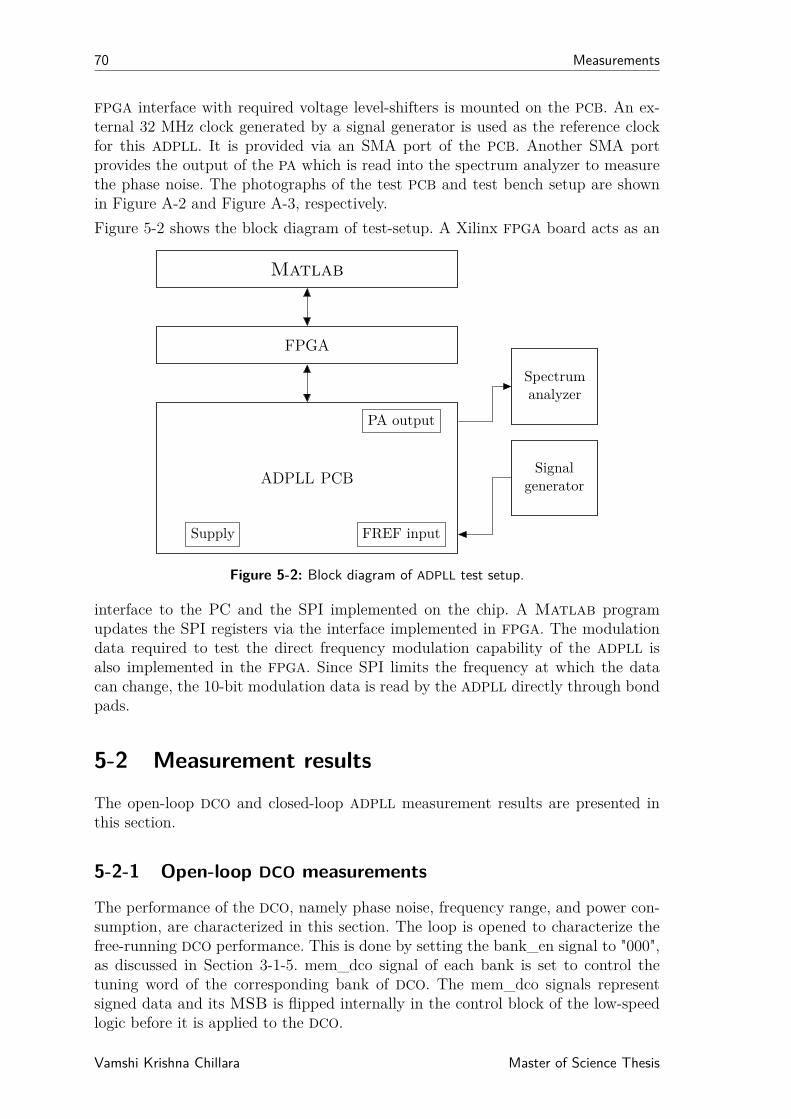
70 Measurements
FPGA interface with required voltage level-shifters is mounted on the PCB. An ex-ternal 32 MHz clock generated by a signal generator is used as the reference clockfor this ADPLL. It is provided via an SMA port of the PCB. Another SMA portprovides the output of the PA which is read into the spectrum analyzer to measurethe phase noise. The photographs of the test PCB and test bench setup are shownin Figure A-2 and Figure A-3, respectively.Figure 5-2 shows the block diagram of test-setup. A Xilinx FPGA board acts as an
Matlab
FPGA
ADPLL PCB
Spectrumanalyzer
Signalgenerator
Supply
PA output
FREF input
Figure 5-2: Block diagram of ADPLL test setup.
interface to the PC and the SPI implemented on the chip. A Matlab programupdates the SPI registers via the interface implemented in FPGA. The modulationdata required to test the direct frequency modulation capability of the ADPLL isalso implemented in the FPGA. Since SPI limits the frequency at which the datacan change, the 10-bit modulation data is read by the ADPLL directly through bondpads.
5-2 Measurement results
The open-loop DCO and closed-loop ADPLL measurement results are presented inthis section.
5-2-1 Open-loop DCO measurements
The performance of the DCO, namely phase noise, frequency range, and power con-sumption, are characterized in this section. The loop is opened to characterize thefree-running DCO performance. This is done by setting the bank_en signal to "000",as discussed in Section 3-1-5. mem_dco signal of each bank is set to control thetuning word of the corresponding bank of DCO. The mem_dco signals representsigned data and its MSB is flipped internally in the control block of the low-speedlogic before it is applied to the DCO.
Vamshi Krishna Chillara Master of Science Thesis

5-2 Measurement results 71
Tuning range
The DCO is designed to cover 2.25 GHz – 2.85 GHz using three banks—5-bit PVT,6-bit acquisition, and 9-bit tracking—to meet the required 2.4 GHz – 2.7 GHz fre-quency range. Figure 5-3 shows the measured frequency of the DCO with varyingPVT and acquisition code at 1 V supply.
0 10 20 30 40 50 60 70
OTW_AB[5:0]
2000
2100
2200
2300
2400
2500
2600
2700
2800
Freq
uency
[M
Hz]
PVT : 0PVT : 4PVT : 8PVT : 12PVT : 16PVT : 20PVT : 24PVT : 28PVT : 31
Figure 5-3: Measured tuning range of the DCO at 1 V supply.
The DCO covers the frequency range of 2.1 GHz – 2.7 GHz. Although the targetfrequency bands are covered, the frequency is shifted by around 150 MHz comparedto the post-layout simulations. One reason could be the change in inductance valuedue to process variations. As discussed in Section 4-1-1, the inductance value canchange by 10% over different corners leading to a frequency shift. Another possibilitycould be the under estimation of the parasitic capacitance by the extraction tool.
The frequency step of the PVT bank is around 11.6 MHz at the lowest operating fre-quency (2.1 GHz) and is 25.7 MHz at the highest operating frequency. At the typicalrunning frequency, 2.4 GHz, the frequency step of the PVT bank is 17 MHz whichis close to the simulated value. The frequency step of acquisition bank is 1.4 MHz,2.3 MHz, and 3.1 MHz at the lowest, typical, and highest operating frequencies, re-spectively. The PVT bank covers a frequency range of 530 MHz while the acquisitionbank has a range of around 150 MHz when operating around 2.4 GHz frequency.
The tuning range of the tracking bank is shown in Figure 5-4. The control wordsof the PVT and acquisition banks are tuned to change the operating frequency toaround 2.44 GHz. The control word for the tracking bank is then swept to obtainits frequency range. It can be seen that the tracking range covers a range of nearly20 MHz. The frequency step is around 40 kHz, slightly lower than that expectedfrom post-layout simulations. The possible reason is the larger parasitics in off-statethan expected from simulations. However, since the range is sufficiently larger thanthe step of acquisition bank, it is not an issue.
Master of Science Thesis Vamshi Krishna Chillara

72 Measurements
0 50 100 150 200 250 300 350 400 450 500
OTW_TB[8:0]
2435
2440
2445
2450
2455
2460
Freq
uency
[M
Hz]
Figure 5-4: Measured tuning range of the tracking bank of the DCO.
Table 5-1 summarizes the measurement results of the frequency range of the threebanks of the digitally controlled oscillator (DCO) at the typical operating frequencyof around 2.4 GHz. We can see that the range of the finer bank is around 7 timesthat of its immediate coarse bank ensuring sufficient overlap between the banks.
Table 5-1: Measurement results of capacitor banks at around 2.4 GHz
PVT Acquisition TrackingNo. of bits 5 6 9Frequency 17 MHz 2.3 MHz 40 kHz
stepFrequency 530 MHz 150 MHz 20 MHz
range
Phase noise and power consumption
The phase noise and power consumption of the oscillator are measured at 2.4 GHzoperating frequency. The DCO bias current is changed by tuning the 5-bit digitalcontrol word as discussed in Section 4-1-2. The measured phase noise of the DCOisshown in Figure 5-5. The DCO has a phase noise of -115.3 at 1 MHz offset for acombined (DCO+buffers) power consumption of 450 µA when operating at 2.46 GHz.
The current can be decreased to trade-off performance by tuning the bias controlword. Figure 5-6 shows the plot of the measured phase noise of DCO as a functionof current consumed of DCO and buffer. Since the DCO buffer and DCO share thesame power supply, the power consumed by the DCO alone could not be measured.A FoM given by Eq. (5-1) is typically used to evaluate the performance of an oscil-lator. It takes into account the power consumption and phase noise to enable a faircomparison.
FoM = L(∆f) + 10 log10
(∆ff0
)2+ 10 log10
(Power1 mW
)(5-1)
Vamshi Krishna Chillara Master of Science Thesis
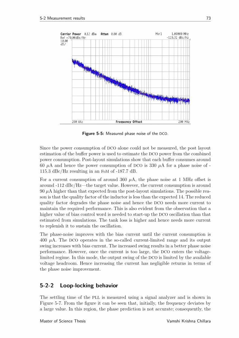
5-2 Measurement results 73
Figure 5-5: Measured phase noise of the DCO.
Since the power consumption of DCO alone could not be measured, the post layoutestimation of the buffer power is used to estimate the DCO power from the combinedpower consumption. Post-layout simulations show that each buffer consumes around60 µA and hence the power consumption of DCO is 330 µA for a phase noise of -115.3 dBc/Hz resulting in an FoM of -187.7 dB.For a current consumption of around 360 µA, the phase noise at 1 MHz offset isaround -112 dBc/Hz—the target value. However, the current consumption is around90 µA higher than that expected from the post-layout simulations. The possible rea-son is that the quality factor of the inductor is less than the expected 14. The reducedquality factor degrades the phase noise and hence the DCO needs more current tomaintain the required performance. This is also evident from the observation that ahigher value of bias control word is needed to start-up the DCO oscillation than thatestimated from simulations. The tank loss is higher and hence needs more currentto replenish it to sustain the oscillation.The phase-noise improves with the bias current until the current consumption is400 µA. The DCO operates in the so-called current-limited range and its outputswing increases with bias current. The increased swing results in a better phase noiseperformance. However, once the current is too large, the DCO enters the voltage-limited regime. In this mode, the output swing of the DCO is limited by the availablevoltage headroom. Hence increasing the current has negligible returns in terms ofthe phase noise improvement.
5-2-2 Loop-locking behavior
The settling time of the PLL is measured using a signal analyzer and is shown inFigure 5-7. From the figure it can be seen that, initially, the frequency deviates bya large value. In this region, the phase prediction is not accurate; consequently, the
Master of Science Thesis Vamshi Krishna Chillara

74 Measurements
-118-117-116-115-114-113-112-111-110-109-108-107
300 350 400 450 500 550 600
PN@
1 M
Hz [d
Bc/H
z]
DCO+Buffer current (µA)
Figure 5-6: Measured phase noise of the DCO versus current.
Bang-bang settling
Outside TDC’s range
Settling behavior
De
mo
du
late
d f
req
ue
ncy
Within
TDC’s range
Figure 5-7: Measured settling behavior of the ADPLL.
phase error is out of narrow range of the TDC. The TDC hence acts like a bang-bangphase detector during this time period. Eventually, the output frequency becomescloser to the target value reducing the phase error to within the TDC’s range. Hencethe frequency deviation and phase noise is small. The ADPLL settles to the targetvalue within 16 µs.
5-2-3 Spectral purity and phase noise
Figure 5-8 shows the spectrum of the ADPLL output clock when the frequency com-mand word (FCW) set to 37.5 corresponding to a target frequency of 2.4 GHz. Thereference spur is quite low at -70 dBc. The fractional spur occurring at 0.5*FREF,which is 16 MHz is also below 65 dBc as it corresponds to a channel with largefractional FCW.The magnitude of the fractional spurs is measured for all the channels that com-
Vamshi Krishna Chillara Master of Science Thesis

5-2 Measurement results 75
prise the Bluetooth Smart, 2.4 GHz – 2.48 GHz with a 2 MHz spacing. They areplotted in Figure 5-9. The worst-case fractional spur is -38 dBc for the near-integer
Fractional spur
Reference spur
Figure 5-8: Output spectrum of theADPLL for FCW = 37.5.
2400 2420 2440 2460 2480
-60
-55
-50
-45
-40
-35Integer channel (FCW=38)
Frequency [MHz]Frequency [MHz]
Frac
tiona
l spu
r [dB
c]
Figure 5-9: Fractional spur overBluetooth Smart channels.
channels. Although this value meets the target requirements (< -30 dBc) it is high.The possible reasons could be the mismatch between the individual delay elementsin the DTC [22]. Several spur-reduction techniques are proposed in the literature toaddress this issue. The FREF dithering employed in [22,23] may be adapted to thisarchitecture in future designs to improve the fractional spur performance.The phase-noise plot of the frequency synthesizer measured using an Agilent 4440Aspectrum analyzer is shown in Figure 5-10 for FCW = 38.125.
Figure 5-10: Measured phase noise of the synthesizer for FCW = 38.125.
The loop band-width is set to around 200 kHz by setting the proportional andintegral constants of the tracking bank, α = 2−5 and ρ = 2−11. The integrated phase
Master of Science Thesis Vamshi Krishna Chillara

76 Measurements
noise between 1 kHz – 100 MHz is 1.7 ps when FCW = 38.125. The phase noise atvery low frequency offsets is dominated by the reference signal. The in-band phasenoise is -90 dBc/Hz and is limited by either the accuracy of DTC gain calibration orthe TDC resolution. The out-of band phase noise at 1 MHz offset is -108.7 dBc/Hz.The phase noise of the synthesizer for far-off integer channel is shown in Figure 5-11 corresponding to an FCW of 37.5. The integrated jitter is 1.38 ps indicating theimprovement possible by applying spur-reduction techniques.
Figure 5-11: Measured phase noise of the synthesizer for FCW = 37.5.
5-2-4 Direct frequency modulation
The implemented ADPLL is capable of direct frequency modulation. It performs 2-point modulation to eliminate the impact of loop-bandwidth on the maximum data-rate achievable. The ADPLL is configured to provide modulation data for the twotargeted standards—ZigBee and Bluetooth Smart. The modulation data is generatedby the FPGA included in the test setup (see Figure 5-2).Figure 5-12 and Figure 5-13 show the 2 Mcps HS-OQPSK modulation provided bythe ADPLL. The ADPLL provides the modulation with 2.3% EVM while fulling thespectral mask requirements.The 1 Mbps GFSK modulation provided by the ADPLL are shown in Figure 5-14and Figure 5-15. The ADPLL provides the modulation with an FSK error of 5.2%(spec. < 20%) and fulfills the spectral mask requirements.
Vamshi Krishna Chillara Master of Science Thesis

5-2 Measurement results 77
Figure 5-12: Measured ZigBee modulation accuracy.
Figure 5-13: Measured ZigBee spectrum.
Master of Science Thesis Vamshi Krishna Chillara
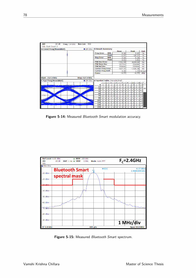
78 Measurements
Figure 5-14: Measured Bluetooth Smart modulation accuracy.
Bluetooth Smart
spectral mask
Bluetooth Smart
spectral mask
FC=2.4GHz
1 MHz/div
Figure 5-15: Measured Bluetooth Smart spectrum.
Vamshi Krishna Chillara Master of Science Thesis

5-2 Measurement results 79
5-2-5 Power consumption
The power break-down of the ADPLL is shown in Table 5-2. The power consumption
Table 5-2: Measured power break-down of the ADPLL.
Power consumption (µW)
DCO+buffer 450low-speed digital 270Divider + 100Phase incrementerTDC+DTC 40
Total 860
of the DCO and buffer is dominant. The high frequency circuits divider and phaseincrementer consume only 100 µW, thanks to the asynchronous counter architec-ture and dynamic logic for the divider. Most importantly, the TDC and DTC, whichperform the fractional phase detection consume only 40 µW compared to the typ-ical mW-level power consumption in time-to-digital converters (TDCs). The phaseprediction and snapshotting techniques enabled the narrow-range low-frequency op-eration of TDC as discussed in Section 2-1. This proves the effectiveness of the DTC-assisted snapshot TDC in reducing the power consumption drastically compared tothe conventional stand-alone TDC. The supply voltage and power consumption canbe further reduced to 0.9 V and 750 µW by trading-off jitter performance (2.2 ps).
5-2-6 Performance summary and comparison
The performance of the ADPLL designed in this work is summarized and comparedto the state-of-the-art PLLs in the literature and is shown in Table 5-3. The totalpower consumption of the ADPLL is 860 µW at 1 V supply for an integrated jitterof 1.7 ps operating at 2.4 GHz. This work achieves the lowest power consumptionamong the multi-GHz ADPLLs published in the literature with a state-of-the-art FoMof -236 dB.Figure 5-16 compares the presented ADPLL with the state-of-the art PLLs in literaturein terms of jitter variance and power consumption. The ADPLLs are denoted inblack. The CP-PLLs with lowest power and highest performance are also depicted (inblue). The jitter2-power FoM is also shown along with the desired direction i.e., toachieve low power and low jitter simultaneously. It is evident that this work presentsthe first sub-mW fractional-N ADPLL and achieves a power consumption at least 5times lower than that of the ADPLLs with similar FoM. Also, this ADPLL occupies3.75 times smaller area compared to its best performing analog counterpart [5] forsimilar applications, indicating its huge potential for cost savings. The sub-mWpower consumption of this ADPLL shows the feasibility of leveraging ADPLLs inultra-low-power applications.
1FoM = 10log10
((σ2
jitter
)∗(
P1mW
))[30]
Master of Science Thesis Vamshi Krishna Chillara

80 Measurements
Table 5-3: Comparison with the state-of-the-art.
This work [5] [12] [43] [42] [45]ISSCC’12 ISSCC’04 ISSCC’11 ISSCC’11 ISSCC’13
Architecture ADPLL CP-PLL ADPLL ADPLL ADPLL ADPLLDTC+TDC Analog TDC-based Bang-Bang Bang-bang TDC-based
Application Bluetooth Bluetooth Bluetooth NA 4G Cellular BluetoothSmart(V4)/ Smart(V4) (V1) EDR(V2)
ZigBee ZiBbee
Technology 40 nm 90 nm 130 nm 65 nm 40 nm 40 nm
Reference 32 MHz 24 MHz 13 MHz 48 MHz 40 MHz 26 MHz
Output (GHz) 2.1–2.7 1.7–2.48 2.4 4.9–6.9 2.9–4.0 2.4RMS Jitter (ps) 1.71 2.66 1.02 0.61 0.56 0.98Power (mW) 0.86 1.1 30 24 4.5 4.55
Supply 1 V 1.2 V 1.5 V 1.2 V 1.2 V 1.3 V
Reference spur -70 dBc -62 dBc -80 dBc -67 dBc -72 dBc -80 dBc
Core area(mm2) 0.2 0.75 0.8 0.91 0.22 0.075PN @ 1 MHz -109 -111 -86@10 kHz -116 -110 -113offset
FM capability Two-point Two-point Two-point No Two-point Two-point
FoM1 (dB) -236 -231 -225 -230 -238.3 -233.6
Figure 5-16: Jitter variance-power plot of state-of-the-art PLLs.
Vamshi Krishna Chillara Master of Science Thesis

Chapter 6
Conclusions
In this thesis, the theory and implementation of an ultra-low-power all-digital phase-locked loop (ADPLL) for frequency synthesis and modulation in ultra-low-powertransceivers is presented. In Chapter 2, it has been shown that TDC remains themain bottleneck in reducing the power consumption of ADPLLs to sub-mW levels.To this end, several low-power techniques are presented.The power consumption is reduced at architecture level by using a combinationof digital-to-time converter (DTC) and time-to-digital converter (TDC) with snap-shotting to replace the traditional power-hungry TDC for fractional phase detection.This reduces the required detection range as well as the operating frequency of theTDC resulting in huge power savings. At the circuit-level, the power consumption ofthe DCO is reduced by using a low-power DCO buffer with tunable voltage transfercharacteristic (VTC). This avoids bulky decoupling capacitors and biasing resistors,thereby reducing the power and area of the DCO plus buffers.The RTL design of the low-speed digital logic and the circuit design and physicallayout of the high speed blocks—DCO, DCO buffer, divider, and phase incrementer—are discussed in detail. To evaluate the effectiveness of the low-power techniquespresented, a prototype is implemented in a TSMC LP 40 nm CMOS process. Thesynthesizer has a measured integrated jitter of 1.7 ps for a power consumption of860 µW leading to a jitter2-power FoM of -236 dB. This is at least 5 dB better thanthat achieved by the published PLLs in literature with similar power consumption [5].The achieved FoM is slightly lower than the best FoM reported for ADPLLs, but hasat least 5x lower consumption. In addition, the prototype ADPLL also supportshigh data-rate frequency modulation, and is demonstrated for ZigBee and BluetoothSmart standards.Figure 6-1 shows the jitter2-power FoM of the state-of-the-art fractional-N ADPLLsplotted as a function of power consumption. This work presents the first RF ADPLLwith a sub-mW power consumption with an FoM close to the state-of-the-art. FromFigure 6-1, it can be observed that high performance ADPLLs tend to have a betterFoM compared to low-power ADPLLs. The presented techniques enable ADPLLs tobreak the sub-mW barrier and thus to be employed in the emerging ultra-low-powerWPAN applications.
Master of Science Thesis 81 Vamshi Krishna Chillara

82 Conclusions
1 10 100
Power [mw]
−245
−240
−235
−230
−225
−220
FoM
[d
B]
This work
ISSCC'11 5.1
Yao JSSC Mar '13
ISSCC'13 19.8
VLSI'11 11.1
VLSI'13 11.2
ISSCC'11 5.3
L. Xu CICC'09
ISSCC'09 5.1
ISSCC'13 20.6
ISSCC'10 26.6
HS Kim JSSC Jul '13
VLSI'09 18.2
ISSCC'12 14.5
ISSCC'11 3.2
ISSCC'10 26.7
ISSCC'11 3.1VLSI'10 14.3
ISSCC'11 5.6
ISSCC'10 26.5
ISSCC'08 19.1
Figure 6-1: FoM versus power consumption of state-of-the-art PLLs.
6-1 Future work
• Although the power consumption of the TDC is reduced drastically, DCO con-sumes considerable power. While the power consumption is limited mainly bythe Q-factor of the on-chip inductor, some improvements are possible. Thebias current of the DCO in this implementation is varied by changing the topresistor. However, the cross-coupled transistors remain unchanged and henceare optimized for only a limited range of bias current. This can be solvedby controlling the number of cross-coupled pair resistor cells attached to theLC-tank instead. Each such cell carries a fixed current and hence the powerconsumption and phase noise are optimum irrespective of the bias current.Also, swing regulation of the DCO should be implemented to ensure constantswing at all frequencies of operation.
• The automatic calibration of DC-coupled DCO buffer should be implemented.One way would be to measure the output duty cycle to control the buffercontrol word so as to maintain the 50% duty-cycle.
• Although the fractional spurs satisfy the requirements of the targeted appli-cation, they are still quite high. One possible way to mitigate the spurs is toincrease the size of the delay cells of DTC to improve matching. Since the DTCconsumes only 2.5% of the total power, increased size would have little impacton the overall power consumption. Also, FREF dithering proposed in [22, 23]may be adapted if needed. In addition, multiple phases of DCO could be ex-ploited to further reduce the DTC range. This reduces the INL and the reducedpower can be traded to further improve the matching performance.
Vamshi Krishna Chillara Master of Science Thesis

Appendix A
Chip pinout, bonding diagram, andmeasurement setup
Table A-1 lists the pinout configuration of the implemented ADPLL prototype. Thebonding diagram with the QFN32 package is shown in Figure A-1. The package hasa metal layer underneath to which numerous down-bonds are made from IC, therebyminimizing the length of grounding bond wires.
56
1
2
3
4
5
6
7
8
24
23
22
21
20
19
18
179 10 11 12 13 14 15 16
32 31 30 29 28 27 26 25
Figure A-1: Bonding diagram of the ADPLL IC.
Master of Science Thesis 83 Vamshi Krishna Chillara

84 Chip pinout, bonding diagram, and measurement setup
Table A-1: Chip pinout of the ADPLL prototype.
Pin number Name Description
1 — Grounded2 TDC_OUT<3>3 TDC_OUT<2> 4-bit TDC4 TDC_OUT<1> output5 TDC_OUT<0>6 PA_CM Buffer calibration7 VDD_PA 1 V PA supply8 VDD_PA 1 V PA supply9 PA_OUT Output clock10 VDD_DIV 1 V divider supply11 NRST Asynchronous reset
acive low12 GND_DIG Digital ground13 VDD_DIG 1 V digital supply14 MOSI SPI Control signal15 MISO SPI Control signal16 SCLK SPI clock17 CS SPI select18 TX_data<9>19 TX_data<8>20 TX_data<7> 10-bit modulation21 TX_data<6> data22 TX_data<5>23 TX_data<4>24 TX_data<3>25 TX_data<2>26 TX_data<1>27 TX_data<0>28 VDD_TDC 1 V TDC supply29 DTC_OUT DTC output
for testing30 TDC_IN TDC input
for testing31 CLK_IN 32 MHz reference32 VDD_DCO 1 V DCO supply
Vamshi Krishna Chillara Master of Science Thesis

85
Measurement setup
The test PCB on which the packaged ADPLL prototype is mounted is shown inFigure A-2. The output clock of the ADPLL is taken out via an SMA connector.External signal generator is used to supply the reference clock and is connected tothe test PCB via another SMA connector. The SPI registers of the ADPLL IC arecontrolled by a Matlab program via FPGA.
To FPGA
Level shifters
ADPLL IC
Matching
network
To PC
Reference clock
Output clockLDO
Figure A-2: Photograph of the test PCB.
The test bench built to characterize the implemented ADPLL prototype is shown inFigure A-3.
FPGA
Power supply
Spectrum analyzer
Signal generator
Figure A-3: Photograph of the test bench setup.
Master of Science Thesis Vamshi Krishna Chillara

86 Chip pinout, bonding diagram, and measurement setup
Vamshi Krishna Chillara Master of Science Thesis

Appendix B
Simulations
B-1 Simulations of the capacitor banks
The post-layout estimations of the quality factor and capacitance step of the capac-itor banks are shown here:
13.323542fA
4.5167448fA
7.5
10.0
Capacitance (fA)
2.5
5.0
12.5
15.0
0.0 .25 .5 .75 1.0Enable voltage
dx: 490.0mdy: 8.8067973fA s: 17.973056fA/
Figure B-1: C–V curve of the unit cell of the PVT bank.
Master of Science Thesis 87 Vamshi Krishna Chillara

88 Simulations
Q:48.621239
Q:594.72906
Quality factor 400.0
0.0
200.0
600.0
0.0 .25 .5 .75 1.0Enable voltage
Figure B-2: Quality factor of the unit cell of the PVT bank.
1.9283622fA
714.13692aA
1.75
.75
.5
1.5
Capacitance (fA)
2.0
1.25
1.0
Enable voltage0.0 .25 .5 .75 1.0
dx: 630.625mdy: 1.2142252fA s: 1.9254315fA/
Figure B-3: C–V curve of the unit cell of the acquisition bank.
Vamshi Krishna Chillara Master of Science Thesis

B-1 Simulations of the capacitor banks 89
2.0489991k
58.134898Quality factor (k)
-.5
0.0
.5
1.0
1.5
2.0
2.5
Enable voltage0.0 .25 .5 .75 1.0
Figure B-4: Quality factor of the unit cell of the acquisition bank.
867.58088aA
850.02236aA850.0
855.0
860.0
865.0
870.0
Capacitance (aA)
Enable voltage0.0 .25 .5 .75 1.0
dx: 659.28571mdy: 17.558512aA s: 26.63263aA/
Figure B-5: C–V curve of the LSB cell of the tracking bank.
Master of Science Thesis Vamshi Krishna Chillara

90 Simulations
66.363873
2.8041433k
Quality factor (k)
2.5
1.5
.5
1.0
3.0
0.0
2.0
.250.0 .5Enable voltage
1.0.75
Figure B-6: Quality factor of the LSB cell of the tracking bank.
758.19795aA
903.23169aA
800.0
825.0
875.0
925.0
750.0
Capacitance (aA)
900.0
850.0
775.0
.250.0 .5Enable voltage
1.0.75
dx: 731.58088mdy: 145.03374aA s: 198.24703aA/
Figure B-7: C–V curve of the MSB cell of the tracking bank.
Vamshi Krishna Chillara Master of Science Thesis

B-1 Simulations of the capacitor banks 91
2.082616k
74.384227
1.0
0.0
2.0
1.5
-.5
Quality factor (k)
2.5
.5
.250.0 .5Enable voltage
1.0.75
Figure B-8: Quality factor of the MSB cell of the tracking bank.
Master of Science Thesis Vamshi Krishna Chillara

92 Simulations
Vamshi Krishna Chillara Master of Science Thesis

Bibliography
[1] V. K. Chillara, Y.-H. Liu, B. Wang, A. Ba, M. Vidojkovic, K. Philips,H. de Groot, and R. B. Staszewski., “An 860µW 2.1-to-2.7GHz All-Digital PLL-Based Frequency Modulator with a DTC-Assisted Snapshot TDC for WPAN(Bluetooth Smart and ZigBee) Applications.” Solid-State Circuits ConferenceDigest of Technical Papers (ISSCC), Feb. 2014. to be published.
[2] C.-H. Park, S. Byun, Y. Song, S. Wang, C. Conroy, and B. Kim, “A low powerCMOS Bluetooth transceiver with a digital offset canceling DLL-based GFSKdemodulator,” in Solid-State Circuits Conference, 2003. Digest of TechnicalPapers. ISSCC. 2003 IEEE International, pp. 96–481 vol.1, 2003.
[3] W. Kluge, F. Poegel, H. Roller, M. Lange, T. Ferchland, L. Dathe, and D. Eg-gert, “A Fully Integrated 2.4-GHz IEEE 802.15.4-Compliant Transceiver forZigBee trade; Applications,” Solid-State Circuits, IEEE Journal of, vol. 41,no. 12, pp. 2767–2775, 2006.
[4] H. Ishikuro, M. Hamada, K.-I. Agawa, S. Kousai, H. Kobayashi, D. M. Nguyen,and F. Hatori, “A single-chip CMOS Bluetooth transceiver with 1.5MHz IFand direct modulation transmitter,” in Solid-State Circuits Conference, 2003.Digest of Technical Papers. ISSCC. 2003 IEEE International, pp. 94–480 vol.1,2003.
[5] Y.-H. Liu, X. Huang, M. Vidojkovic, A. Ba, P. Harpe, G. Dolmans, andH. de Groot, “A 1.9nJ/b 2.4GHz multistandard (Bluetooth Low Energy/Zig-bee/IEEE802.15.6) transceiver for personal/body-area networks,” in Solid-StateCircuits Conference Digest of Technical Papers (ISSCC), 2013 IEEE Interna-tional, pp. 446–447, 2013.
[6] S. Kashmiri, M. A. P. Pertijs, and K. Makinwa, “A Thermal-Diffusivity-BasedFrequency Reference in Standard CMOS With an Absolute Inaccuracy of 0.155C to 125 C,” Solid-State Circuits, IEEE Journal of, vol. 45, no. 12, pp. 2510–2520, 2010.
[7] M. Lutz, A. Partridge, P. Gupta, N. Buchan, E. Klaassen, J. McDonald, andK. Petersen, “MEMS Oscillators for High Volume Commercial Applications,” in
Master of Science Thesis 93 Vamshi Krishna Chillara

94 Bibliography
Solid-State Sensors, Actuators and Microsystems Conference, 2007. TRANS-DUCERS 2007. International, pp. 49–52, 2007.
[8] C. S. Lam, “A review of the recent development of MEMS and crystal oscillatorsand their impacts on the frequency control products industry,” in UltrasonicsSymposium, 2008. IUS 2008. IEEE, pp. 694–704, 2008.
[9] F. M. Gardner, “Charge-Pump Phase-Lock Loops,” Communications, IEEETransactions on, vol. 28, no. 11, pp. 1849–1858, 1980.
[10] R. Staszewski, J. Wallberg, C.-M. Hung, G. Feygin, M. Entezari, andD. Leipold, “LMS-based calibration of an RF digitally controlled oscillator formobile phones,” Circuits and Systems II: Express Briefs, IEEE Transactionson, vol. 53, no. 3, pp. 225–229, 2006.
[11] R.B.Staszewski, Digital deep-submicron CMOS frequency synthesis for RF wire-less applications. Phd thesis, University of Texas, Dallas, 2002.
[12] R. Staszewski, K. Muhammad, D. Leipold, C.-M. Hung, Y.-C. Ho, J. Wall-berg, C. Fernando, K. Maggio, R. Staszewski, T. Jung, J. Koh, S. John,I. Y. Deng, V. Sarda, O. Moreira-Tamayo, V. Mayega, R. Katz, O. Friedman,O. Eliezer, E. de Obaldia, and P. Balsara, “All-digital TX frequency synthesizerand discrete-time receiver for Bluetooth radio in 130-nm CMOS,” Solid-StateCircuits, IEEE Journal of, vol. 39, no. 12, pp. 2278–2291, 2004.
[13] R. Staszewski, D. Leipold, O. Eliezer, M. Entezari, K. Muhammad, I. Bashir,C. M. Hung, J. Wallberg, R. Staszewski, P. Cruise, S. Rezeq, S. Vemulapalli,K. Waheed, N. Barton, M. C. Lee, C. Fernando, K. Maggio, T. Jung, I. Elahi,S. Larson, T. Murphy, G. Feygin, I. Deng, T. Mayhugh, Y. C. Ho, K. M. Low,C. Lin, J. Jaehnig, J. Kerr, J. Mehta, S. Glock, T. Almholt, and S. Bhatara, “A24mm2 Quad-Band Single-Chip GSM Radio with Transmitter Calibration in90nm Digital CMOS,” in Solid-State Circuits Conference, 2008. ISSCC 2008.Digest of Technical Papers. IEEE International, pp. 208–607, 2008.
[14] J. Mehta, R. Staszewski, O. Eliezer, S. Rezeq, K. Waheed, M. Entezari, G. Fey-gin, S. Vemulapalli, V. Zoicas, C.-M. Hung, N. Barton, I. Bashir, K. Maggio,M. Frechette, M.-C. Lee, J. Wallberg, P. Cruise, and N. Yanduru, “A 0.8mm2
all-digital SAW-less polar transmitter in 65nm EDGE SoC,” in Solid-State Cir-cuits Conference Digest of Technical Papers (ISSCC), 2010 IEEE International,pp. 58–59, 2010.
[15] H.-H. Chang, P.-Y. Wang, J.-H. Zhan, and B.-Y. Hsieh, “A Fractional Spur-Free ADPLL with Loop-Gain Calibration and Phase-Noise Cancellation forGSM/GPRS/EDGE,” in Solid-State Circuits Conference, 2008. ISSCC 2008.Digest of Technical Papers. IEEE International, pp. 200–606, 2008.
[16] L. Fanori, A. Liscidini, and R. Castello, “3.3GHz DCO with a frequency reso-lution of 150Hz for All-digital PLL,” in Solid-State Circuits Conference Digestof Technical Papers (ISSCC), 2010 IEEE International, pp. 48–49, 2010.
Vamshi Krishna Chillara Master of Science Thesis

95
[17] R. Staszewski, C.-M. Hung, D. Leipold, and P. Balsara, “A first multigigahertzdigitally controlled oscillator for wireless applications,” Microwave Theory andTechniques, IEEE Transactions on, vol. 51, no. 11, pp. 2154–2164, 2003.
[18] R. Staszewski, S. Vemulapalli, P. Vallur, J. Wallberg, and P. Balsara, “1.3 V 20ps time-to-digital converter for frequency synthesis in 90-nm CMOS,” Circuitsand Systems II: Express Briefs, IEEE Transactions on, vol. 53, no. 3, pp. 220–224, 2006.
[19] M. Lee, M. Heidari, and A. Abidi, “A low noise, wideband digital phase-lockedloop based on a new time-to-digital converter with subpicosecond resolution,”in VLSI Circuits, 2008 IEEE Symposium on, pp. 112–113, 2008.
[20] C.-M. Hsu, M. Straayer, and M. Perrott, “A Low-Noise, Wide-BW 3.6GHzDigital ∆Σ Fractional-N Frequency Synthesizer with a Noise-Shaping Time-to-Digital Converter and Quantization Noise Cancellation,” in Solid-State Cir-cuits Conference, 2008. ISSCC 2008. Digest of Technical Papers. IEEE Inter-national, pp. 340–617, 2008.
[21] A. Liscidini, L. Vercesi, and R. Castello, “Time to digital converter based on a2-dimensions Vernier architecture,” in Custom Integrated Circuits Conference,2009. CICC ’09. IEEE, pp. 45–48, 2009.
[22] E. Temporiti, C. Weltin-Wu, D. Baldi, R. Tonietto, and F. Svelto, “A 3 GHzFractional All-Digital PLL With a 1.8 MHz Bandwidth Implementing SpurReduction Techniques,” Solid-State Circuits, IEEE Journal of, vol. 44, no. 3,pp. 824–834, 2009.
[23] R. Staszewski, K. Waheed, F. Dulger, and O. Eliezer, “Spur-Free Multirate All-Digital PLL for Mobile Phones in 65 nm CMOS,” Solid-State Circuits, IEEEJournal of, vol. 46, no. 12, pp. 2904–2919, 2011.
[24] R. Staszewski, “State-of-the-art and future directions of high-performance all-digital frequency synthesis in nanometer CMOS,” in Circuits and Systems (IS-CAS), Proceedings of 2010 IEEE International Symposium on, pp. 229–232,2010.
[25] M. Vidojkovic, Y.-H. Liu, X. Huang, K. Imamura, G. Dolmans, andH. De Groot, “A fully integrated 1.7–2.5GHz 1mW fractional-N PLL for WBANand WSN applications,” in Radio Frequency Integrated Circuits Symposium(RFIC), 2012 IEEE, pp. 185–188, 2012.
[26] D. Park, W. Lee, S. Jeon, and S. Cho, “A 2.5-GHz 860 µW charge-recyclingfractional-N frequency synthesizer in 130nm CMOS,” in VLSI Circuits, 2008IEEE Symposium on, pp. 88–89, 2008.
[27] G. Devita, A. C. W. Wong, N. Kasparidis, P. Corbishley, A. Burdett, andP. Paddan, “A 0.9mW PLL integrated in an ultra-low-power SoC for WPANand WBAN applications,” in ESSCIRC, 2010 Proceedings of the, pp. 158–161,2010.
Master of Science Thesis Vamshi Krishna Chillara

96 Bibliography
[28] A. Italia and G. Palmisano, “A 1.2-mW CMOS frequency synthesizer with fully-integrated LC VCO for 400-MHz medical implantable transceivers,” in RadioFrequency Integrated Circuits Symposium, 2009. RFIC 2009. IEEE, pp. 333–336, 2009.
[29] W.-H. Chen, W.-F. Loke, G. Thompson, and B. Jung, “A 0.5-V, 440µW fre-quency synthesizer for implantable medical devices,” in Custom Integrated Cir-cuits Conference (CICC), 2011 IEEE, pp. 1–4, 2011.
[30] X. Gao, E. Klumperink, M. Bohsali, and B. Nauta, “A 2.2GHz 7.6mW sub-sampling PLL with −126dBc/Hz in-band phase noise and 0.15psrms jitter in0.18µm CMOS,” in Solid-State Circuits Conference - Digest of Technical Pa-pers, 2009. ISSCC 2009. IEEE International, pp. 392–393,393a, 2009.
[31] R. Staszewski, C.-M. Hung, K. Maggio, J. Wallberg, D. Leipold, and P. Balsara,“All-digital phase-domain TX frequency synthesizer for Bluetooth radios in0.13 µ m CMOS,” in Solid-State Circuits Conference, 2004. Digest of TechnicalPapers. ISSCC. 2004 IEEE International, pp. 272–527 Vol.1, 2004.
[32] R. B. Staszewski and P. T. Balsara, All-Digital Frequency Synthesizer in Deep-Submicron CMOS. Wiley-Interscience, 2006.
[33] E. Temporiti, G. Albasini, I. Bietti, R. Castello, and M. Colombo, “A 700-khzbandwidth sigma; delta; fractional synthesizer with spurs compensation andlinearization techniques for wcdma applications,” Solid-State Circuits, IEEEJournal of, vol. 39, no. 9, pp. 1446–1454, 2004.
[34] L. Xu, S. Lindfors, K. Stadius, and J. Ryynanen, “A 2.4-GHz low-power all-digital phase-locked loop,” in Custom Integrated Circuits Conference, 2009.CICC ’09. IEEE, pp. 331–334, 2009.
[35] W. R. Bennett, “Spectra of quantized signals,” Bell System Technical Journal,vol. 27, no. 3, pp. 446–472, 1948.
[36] P. Dudek, S. Szczepanski, and J. Hatfield, “A high-resolution cmos time-to-digital converter utilizing a vernier delay line,” Solid-State Circuits, IEEE Jour-nal of, vol. 35, no. 2, pp. 240–247, 2000.
[37] M. Perrott, I. Tewksbury, T.L., and C. Sodini, “A 27-mw cmos fractional-nsynthesizer using digital compensation for 2.5-mb/s gfsk modulation,” Solid-State Circuits, IEEE Journal of, vol. 32, no. 12, pp. 2048–2060, 1997.
[38] R. A. Meyers and P. H. Waters, “Synthesiser review for pan-european digitalcellular radio,” in VLSI Implementations for Second Generation Digital Cord-less and Mobile Telecommunication Systems, IEE Colloquium on, pp. 8/1–810,1990.
[39] M. Bopp, M. Alles, M. Arens, D. Eichel, S. Gerlach, R. Gotzfried, F. Gruson,M. Kocks, G. Krimmer, R. Reimann, B. Roos, M. Siegle, and J. Zieschang, “Adect transceiver chip set using sige technology,” in Solid-State Circuits Con-ference, 1999. Digest of Technical Papers. ISSCC. 1999 IEEE International,pp. 68–69, 1999.
Vamshi Krishna Chillara Master of Science Thesis

97
[40] M. Ferriss and M. Flynn, “A 14mW Fractional-N PLL Modulator with an En-hanced Digital Phase Detector and Frequency Switching Scheme,” in Solid-StateCircuits Conference, 2007. ISSCC 2007. Digest of Technical Papers. IEEE In-ternational, pp. 352–608, 2007.
[41] W. Khalil, S. Shashidharan, T. Copani, S. Chakraborty, S. Kiaei, andB. Bakkaloglu, “A 700-µA 405-MHz All-Digital Fractional-N Frequency-LockedLoop for ISM Band Applications,” Microwave Theory and Techniques, IEEETransactions on, vol. 59, no. 5, pp. 1319–1326, 2011.
[42] D. Tasca, M. Zanuso, G. Marzin, S. Levantino, C. Samori, and A. L. Lacaita,“A 2.9-4.0-GHz Fractional-N Digital PLL With Bang-Bang Phase Detector and560-fsrms Integrated Jitter at 4.5-mW Power,” J. Solid-State Circuits, vol. 46,no. 12, pp. 2745–2758, 2011.
[43] N. Pavlovic and J. Bergervoet, “A 5.3GHz digital-to-time-converter-basedfractional-N all-digital PLL,” in Solid-State Circuits Conference Digest of Tech-nical Papers (ISSCC), 2011 IEEE International, pp. 54–56, 2011.
[44] J. Zhuang and R. Staszewski, “A low-power all-digital PLL architecture basedon phase prediction,” in Electronics, Circuits and Systems (ICECS), 2012 19thIEEE International Conference on, pp. 797–800, 2012.
[45] J. wei Lai, C.-H. Wang, K. Kao, A. Lin, Y.-H. Cho, L. Cho, M.-H. Hung, X.-Y. Shih, C.-M. Lin, S.-H. Yan, Y.-H. Chung, P. Liang, G.-K. Dehng, H.-S. Li,G. Chien, and R. Staszewski, “A 0.27mm2 13.5dBm 2.4GHz all-digital polartransmitter using 34Solid-State Circuits Conference Digest of Technical Papers(ISSCC), 2013 IEEE International, pp. 342–343, 2013.
[46] T. Tokairin, M. Okada, M. Kitsunezuka, T. Maeda, and M. Fukaishi, “A 2.1-to-2.8GHz all-digital frequency synthesizer with a time-windowed TDC,” in Solid-State Circuits Conference Digest of Technical Papers (ISSCC), 2010 IEEE In-ternational, pp. 470–471, 2010.
[47] M. Park, M. Perrott, and R. Staszewski, “An Amplitude Resolution Improve-ment of an RF-DAC Employing Pulsewidth Modulation,” Circuits and SystemsI: Regular Papers, IEEE Transactions on, vol. 58, no. 11, pp. 2590–2603, 2011.
[48] J. Zhuang and R. Staszewski, “Gain estimation of a digital-to-time converterfor phase-prediction all-digital PLL,” in Circuit Theory and Design (ECCTD),2013 21st European Conference on, 2013.
[49] K. Waheed and R. Staszewski, “Time-domain behavioral modeling of a multi-gigahertz digital rf oscillator using vhdl,” in Circuits and Systems, 2005. 48thMidwest Symposium on, pp. 1669–1672 Vol. 2, 2005.
[50] A. Ismail and A. Abidi, “CMOS differential LC oscillator with suppressed up-converted flicker noise,” in Solid-State Circuits Conference, 2003. Digest ofTechnical Papers. ISSCC. 2003 IEEE International, pp. 98–99 vol.1, 2003.
[51] P. Andreani and S. Mattisson, “On the use of MOS varactors in RF VCOs,”Solid-State Circuits, IEEE Journal of, vol. 35, no. 6, pp. 905–910, 2000.
Master of Science Thesis Vamshi Krishna Chillara

98 Bibliography
[52] W. Jiang, A. Tavakol, P. Effendrik, M. van de Gevel, F. Verwaal, andR. Staszewski, “Design of ADPLL system for WiMAX applications in 40-nmCMOS,” in Electronics, Circuits and Systems (ICECS), 2012 19th IEEE Inter-national Conference on, pp. 73–76, 2012.
[53] C.-M. Hung, R. Staszewski, N. Barton, M.-C. Lee, and D. Leipold, “A digitallycontrolled oscillator system for SAW-less transmitters in cellular handsets,”Solid-State Circuits, IEEE Journal of, vol. 41, no. 5, pp. 1160–1170, 2006.
Vamshi Krishna Chillara Master of Science Thesis

Glossary
List of Acronyms
ADC analog-to-digital converter
ADPLL all-digital phase-locked loop
BBPLL bang-bang phase-locked loop
CKR re-timed reference
CKV variable clock
CMOS complementary metal-oxide-semiconductor
CP-PLL charge-pump phase-locked loop
DCO digitally controlled oscillator
DIBL drain-induced barrier lowering
DTC digital-to-time converter
FCW frequency command word
FoM figure-of-merit
FPGA field programmable gate array
FSM finite state machine
IF intermediate frequency
LDO low-dropout
LNA low-noise amplifier
LO local oscillator
MICS medical implant communication service
OTW oscillator tuning word
Master of Science Thesis 99 Vamshi Krishna Chillara

100 Glossary
PCB printed circuit board
PGA programmable gain amplifier
PLL phase-locked loop
PVT process, voltage, and temperature
PA power amplifier
RF radio frequency
SNR signal-to-noise ratio
TDC time-to-digital converter
VCO voltage-controlled oscillator
VTC voltage transfer characteristic
WBAN wireless body area network
WPAN wireless personal area network
Vamshi Krishna Chillara Master of Science Thesis