various soc-related applications, business models, global industries & careerlife planning
TRANSCRIPT
Various SoC-Related Applications, Business
Models, Global Industries & CareerLife Planning
Four Major Technology Drivers
• RF and AMS• SoC• MPU• (Embedded) Memory
RF and AMS (Analog/Mixed Signal)
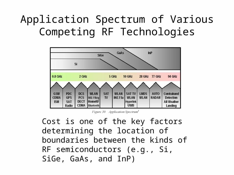
Application Spectrum of Various Competing RF Technologies
Cost is one of the key factors determining the location of boundaries between the kinds of RF semiconductors (e.g., Si, SiGe, GaAs, and InP)
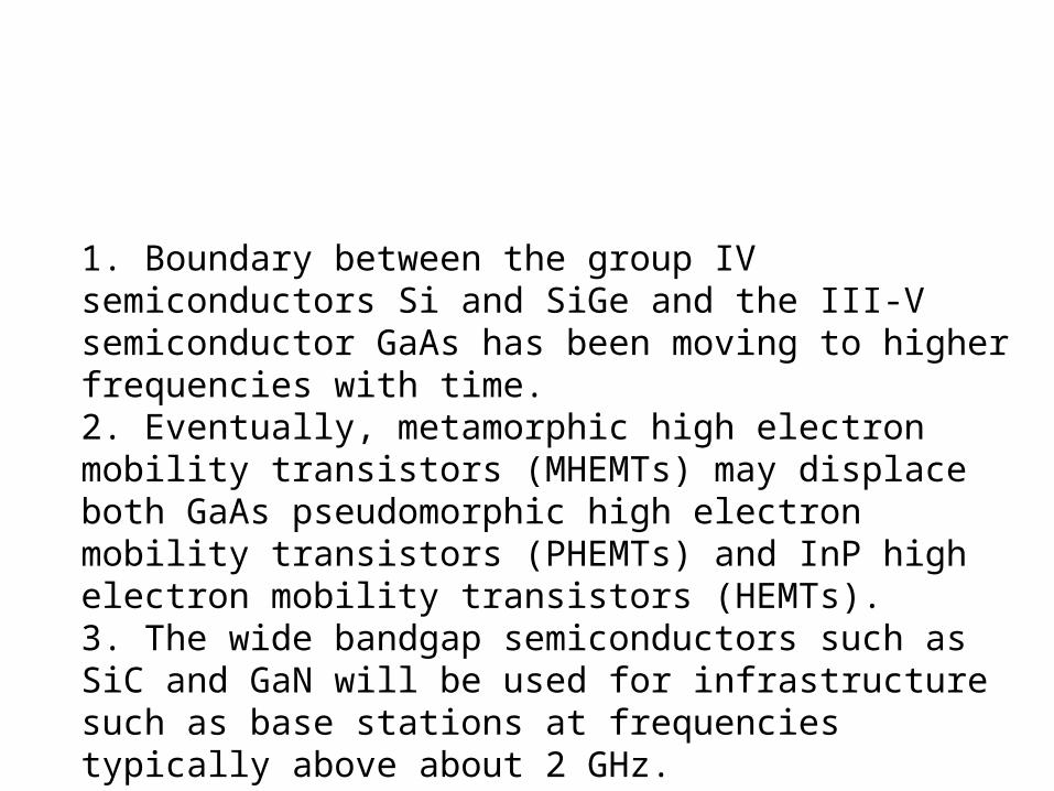
1. Boundary between the group IV semiconductors Si and SiGe and the III-V semiconductor GaAs has been moving to higher frequencies with time. 2. Eventually, metamorphic high electron mobility transistors (MHEMTs) may displace both GaAs pseudomorphic high electron mobility transistors (PHEMTs) and InP high electron mobility transistors (HEMTs). 3. The wide bandgap semiconductors such as SiC and GaN will be used for infrastructure such as base stations at frequencies typically above about 2 GHz.
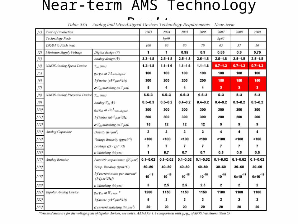
Near-term AMS Technology Req’t
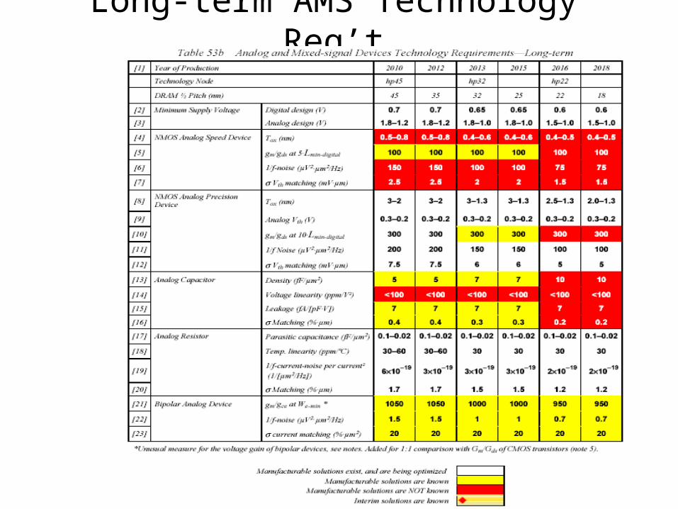
Long-term AMS Technology Req’t
1. Standards and protocols influence considerably parameters such as operating frequencies, channel bandwidth, and transmit power.
2. Increased RF performance for silicon is usually achieved by geometrical scaling. Increased RF performance for III-V compound semiconductors is achieved by optimizing carrier transport properties through materials and bandgap engineering.
3. During the last two decades, technologies based on III-V compounds have established new business opportunities for wireless communications systems.
4. When high volumes of product are expected, silicon and more recently silicon-germanium replace the III-Vs in those markets for which these group IVs can deliver appropriate performance at low cost.
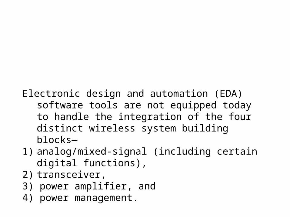
Electronic design and automation (EDA) software tools are not equipped today to handle the integration of the four distinct wireless system building blocks—
1) analog/mixed-signal (including certain digital functions),
2) transceiver,3) power amplifier, and 4) power management.
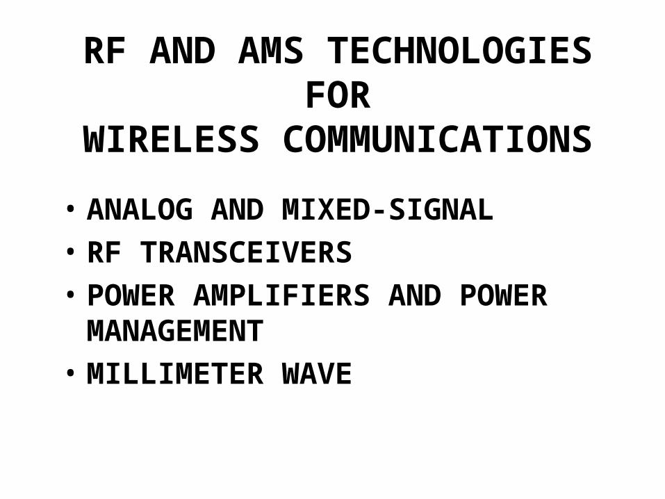
RF AND AMS TECHNOLOGIES FOR
WIRELESS COMMUNICATIONS
• ANALOG AND MIXED-SIGNAL• RF TRANSCEIVERS• POWER AMPLIFIERS AND
POWER MANAGEMENT• MILLIMETER WAVE
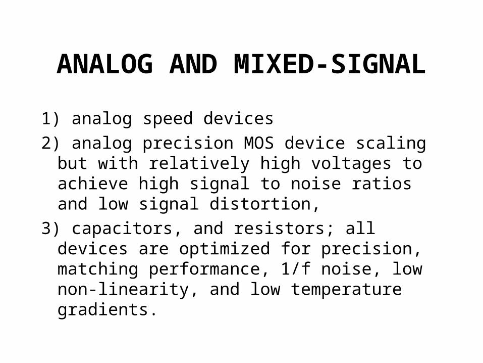
ANALOG AND MIXED-SIGNAL
1) analog speed devices 2) analog precision MOS device scaling but
with relatively high voltages to achieve high signal to noise ratios and low signal distortion,
3) capacitors, and resistors; all devices are optimized for precision, matching performance, 1/f noise, low non-linearity, and low temperature gradients.
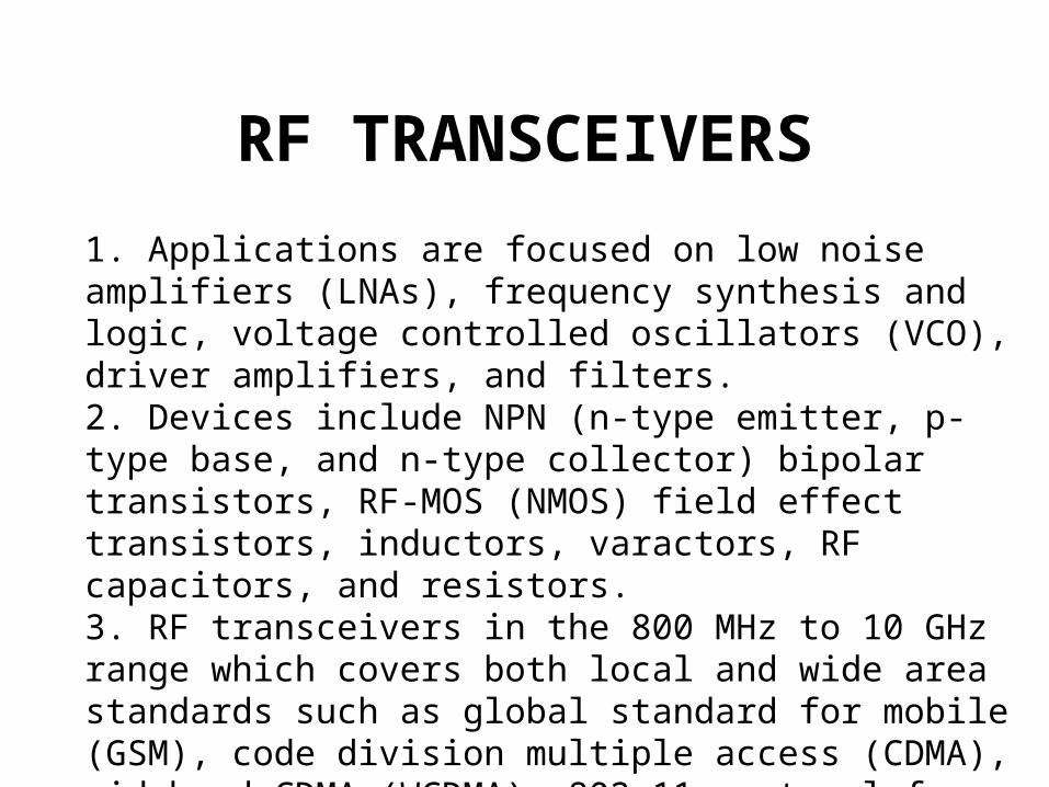
RF TRANSCEIVERS
1. Applications are focused on low noise amplifiers (LNAs), frequency synthesis and logic, voltage controlled oscillators (VCO), driver amplifiers, and filters. 2. Devices include NPN (n-type emitter, p-type base, and n-type collector) bipolartransistors, RF-MOS (NMOS) field effect transistors, inductors, varactors, RF capacitors, and resistors. 3. RF transceivers in the 800 MHz to 10 GHz range which covers both local and wide area standards such as global standard for mobile (GSM), code division multiple access (CDMA), wideband CDMA (WCDMA), 802.11 protocol for local area networks, and ultra wideband (UWB).
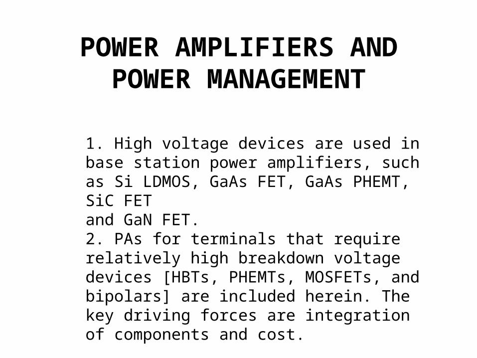
POWER AMPLIFIERS AND POWER MANAGEMENT
1. High voltage devices are used in base station power amplifiers, such as Si LDMOS, GaAs FET, GaAs PHEMT, SiC FETand GaN FET. 2. PAs for terminals that require relatively high breakdown voltage devices [HBTs, PHEMTs, MOSFETs, and bipolars] are included herein. The key driving forces are integration of components and cost.
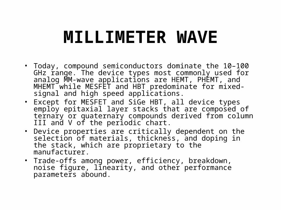
MILLIMETER WAVE
• Today, compound semiconductors dominate the 10–100 GHz range. The device types most commonly used for analog MM-wave applications are HEMT, PHEMT, and MHEMT while MESFET and HBT predominate for mixed-signal and high speed applications.
• Except for MESFET and SiGe HBT, all device types employ epitaxial layer stacks that are composed of ternary or quaternary compounds derived from column III and V of the periodic chart.
• Device properties are critically dependent on the selection of materials, thickness, and doping in the stack, which are proprietary to the manufacturer.
• Trade-offs among power, efficiency, breakdown, noise figure, linearity, and other performance parameters abound.
1. Manufacturing non-recurring engineering (NRE) costs are on the order of one million dollars (mask set + probe card); design NRE costs routinely reach tens of millions of dollars, with design shortfalls being responsible for silicon re-spins that multiply manufacturing NRE.
2. Manufacturing cycle times are measured in weeks, with low uncertainty; Design and verification cycle times are measured in months or years, with high uncertainty.
3. Software can account for 80% of embedded-systems development cost;
Test cost has grown exponentially relative to manufacturing cost;
Verification engineers outnumber design engineers on microprocessor project teams.
Challenges due to Silicon complexity ; impact of process scaling, new materials
or device/interconnect architectures
1. Non-ideal scaling of device parasitics and supply/threshold voltages (leakage, power management, circuit/device innovation, current delivery)
2. Coupled high-frequency devices and interconnects (noise/interference, signal integrity analysis and management, substrate coupling, delay variation due to cross-coupling)
3. Manufacturing variability (statistical process modeling and characterization, yield, leakage power)
4. Scaling of global interconnect performance relative to device performance (communication, synchronization)
5. Decreased reliability (gate insulator tunneling and breakdown integrity, joule heating and electromigration, single-event upset, general fault-tolerance)
6. Complexity of manufacturing handoff (reticle enhancement and mask writing/inspection flow, NRE cost).
7. Process variability (library characterization, analog and digital circuit performance, error-tolerant design, layout reuse, reliable and predictable implementation platforms)
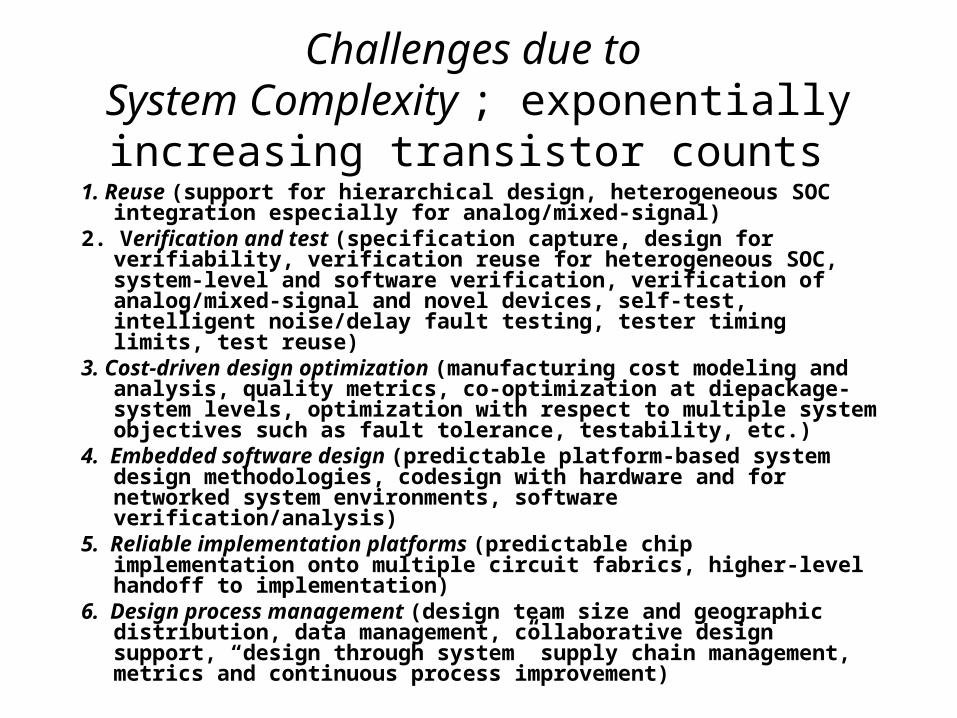
Challenges due to System Complexity ; exponentially
increasing transistor counts 1. Reuse (support for hierarchical design, heterogeneous SOC
integration especially for analog/mixed-signal)2. Verification and test (specification capture, design for
verifiability, verification reuse for heterogeneous SOC, system-level and software verification, verification of analog/mixed-signal and novel devices, self-test, intelligent noise/delay fault testing, tester timing limits, test reuse)
3. Cost-driven design optimization (manufacturing cost modeling and analysis, quality metrics, co-optimization at diepackage-system levels, optimization with respect to multiple system objectives such as fault tolerance, testability, etc.)
4. Embedded software design (predictable platform-based system design methodologies, codesign with hardware and for networked system environments, software verification/analysis)
5. Reliable implementation platforms (predictable chip implementation onto multiple circuit fabrics, higher-level handoff to implementation)
6. Design process management (design team size and geographic distribution, data management, collaborative design support, “design through system” supply chain management, metrics and continuous process improvement)
SoC
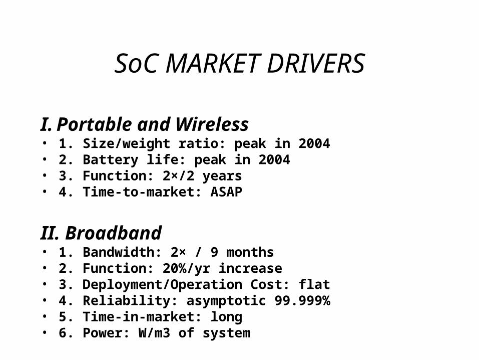
SoC MARKET DRIVERS
I. Portable and Wireless• 1. Size/weight ratio: peak in 2004• 2. Battery life: peak in 2004• 3. Function: 2×/2 years• 4. Time-to-market: ASAP
II. Broadband• 1. Bandwidth: 2× / 9 months• 2. Function: 20%/yr increase• 3. Deployment/Operation Cost: flat• 4. Reliability: asymptotic 99.999%• 5. Time-in-market: long• 6. Power: W/m3 of system
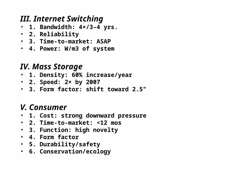
III. Internet Switching• 1. Bandwidth: 4×/3–4 yrs.• 2. Reliability• 3. Time-to-market: ASAP• 4. Power: W/m3 of system
IV. Mass Storage• 1. Density: 60% increase/year• 2. Speed: 2× by 2007• 3. Form factor: shift toward 2.5"
V. Consumer• 1. Cost: strong downward pressure• 2. Time-to-market: <12 mos• 3. Function: high novelty• 4. Form factor• 5. Durability/safety• 6. Conservation/ecology
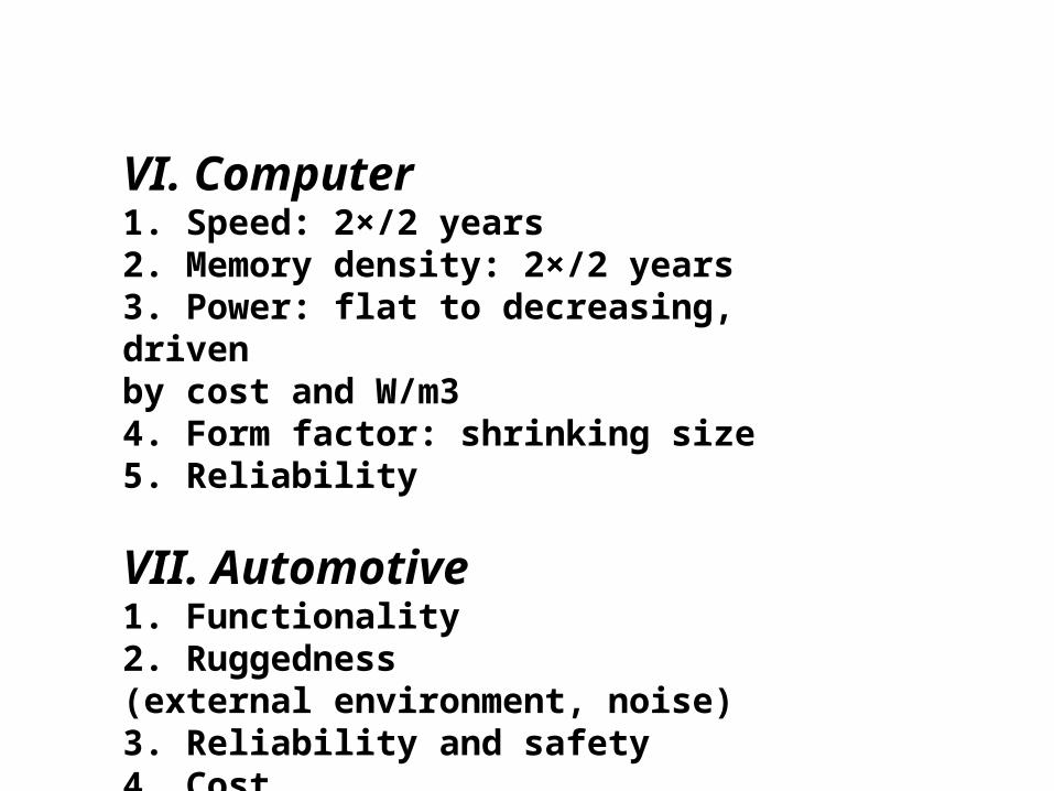
VI. Computer1. Speed: 2×/2 years2. Memory density: 2×/2 years3. Power: flat to decreasing, drivenby cost and W/m34. Form factor: shrinking size5. Reliability
VII. Automotive1. Functionality2. Ruggedness(external environment, noise)3. Reliability and safety4. Cost
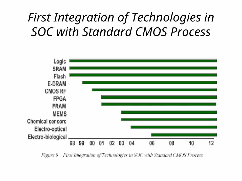
First Integration of Technologies in SOC with Standard CMOS
Process
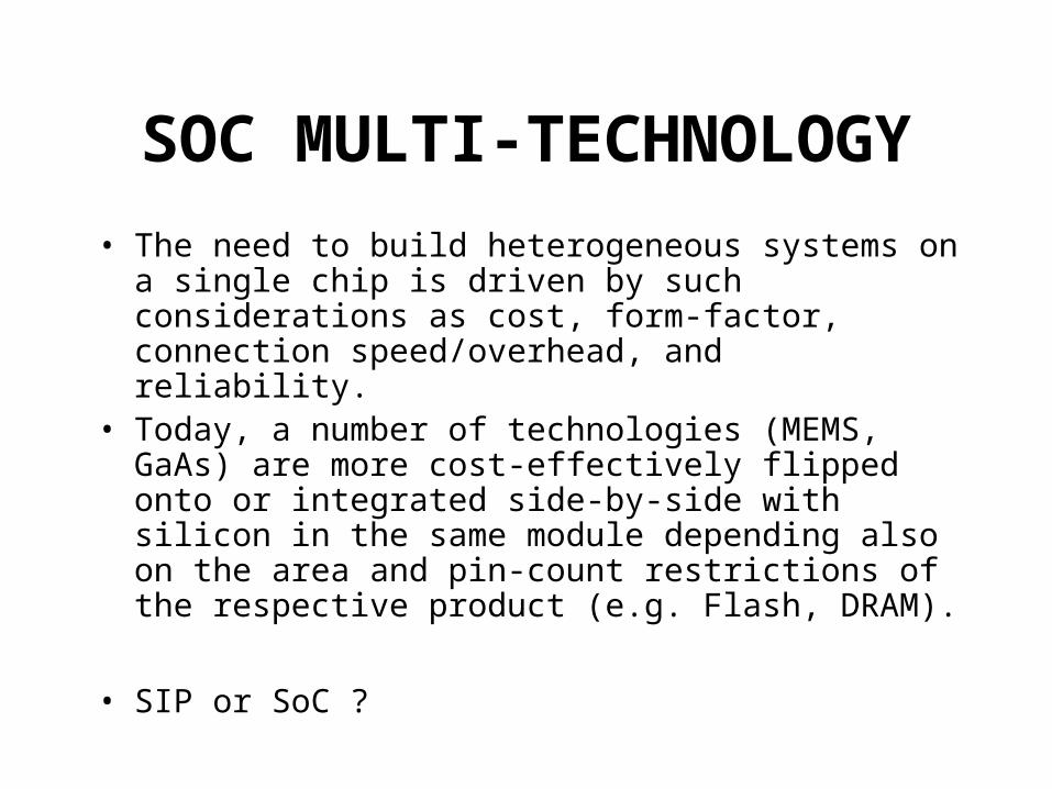
SOC MULTI-TECHNOLOGY
• The need to build heterogeneous systems on a single chip is driven by such considerations as cost, form-factor, connection speed/overhead, and reliability.
• Today, a number of technologies (MEMS, GaAs) are more cost-effectively flipped onto or integrated side-by-side with silicon in the same module depending also on the area and pin-count restrictions of the respective product (e.g. Flash, DRAM).
• SIP or SoC ?
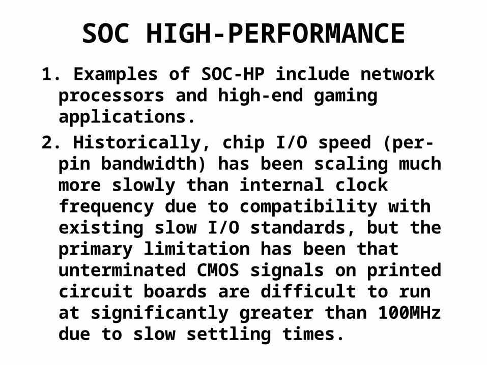
SOC HIGH-PERFORMANCE1. Examples of SOC-HP include
network processors and high-end gaming applications.
2. Historically, chip I/O speed (per-pin bandwidth) has been scaling much more slowly than internal clock frequency due to compatibility with existing slow I/O standards, but the primary limitation has been that unterminated CMOS signals on printed circuit boards are difficult to run at significantly greater than 100MHz due to slow settling times.
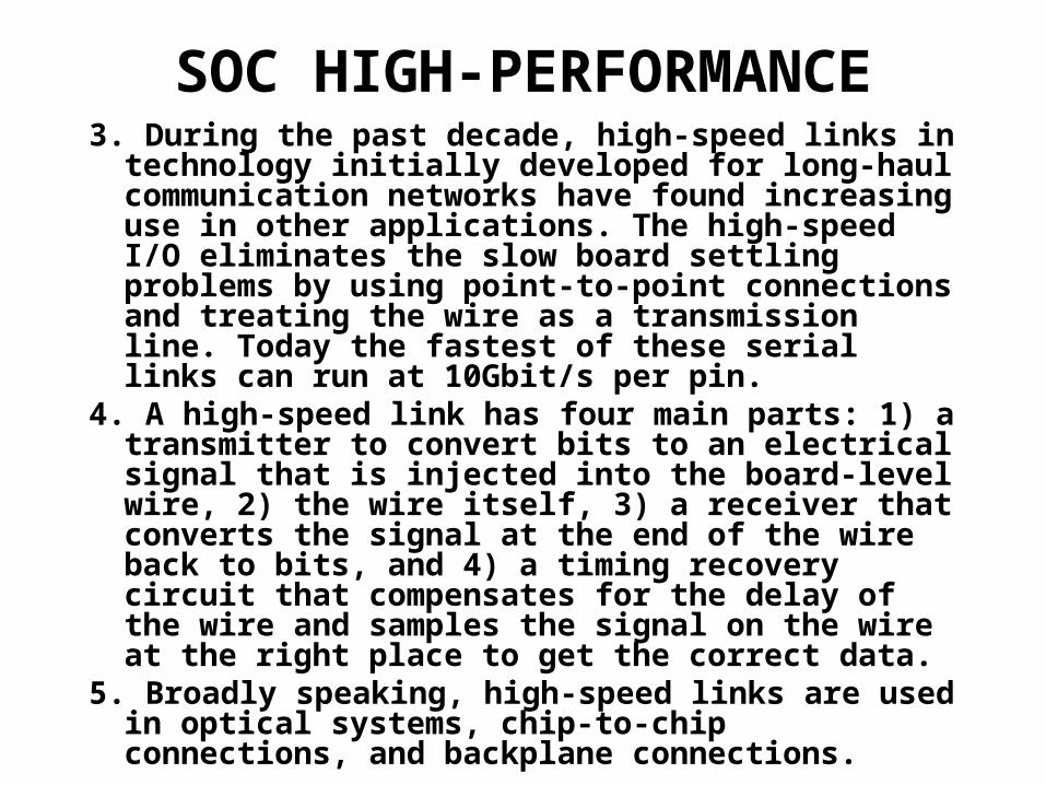
SOC HIGH-PERFORMANCE3. During the past decade, high-speed links in
technology initially developed for long-haul communication networks have found increasing use in other applications. The high-speed I/O eliminates the slow board settling problems by using point-to-point connections and treating the wire as a transmission line. Today the fastest of these serial links can run at 10Gbit/s per pin.
4. A high-speed link has four main parts: 1) a transmitter to convert bits to an electrical signal that is injected into the board-level wire, 2) the wire itself, 3) a receiver that converts the signal at the end of the wire back to bits, and 4) a timing recovery circuit that compensates for the delay of the wire and samples the signal on the wire at the right place to get the correct data.
5. Broadly speaking, high-speed links are used in optical systems, chip-to-chip connections, and backplane connections.
SOC LOW-COST, LOW-POWER
1. Examples of SOC-LP include portable and wireless applications such as PDAs or digital camera chips.
2. LOP(Low Operating Power) and LSTP(Low Standby Power)
SoC-related Business Models
– Foundry
– Independent Device Manufacturer (IDM)
– ASSP Provider (Fabless)
– IP Provider (Chipless)
– System House
– Design Service Providers (Design House)
– EDA Vendors
– Embedded Software Developers
– Assembly House (Chipak, ASE, Anam)
– Others
• Mask House (Dupont,…)
• Equipment Manufacturer
• Wafer/Materials Supplier
Foundry
– Silicon foundry offers 0.09+ micron digital + analog, RF, MEMS …
– long IP (free, priced) list desirable
– MPW runs for prototyping
– Reticle generation + fabrication
– P&R, testing, packaging service extra
– TSMC, UMC, Chartered, SMIC, Dongbu-Anam,..
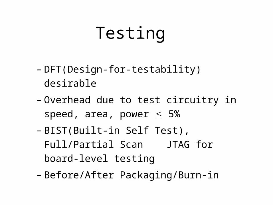
Testing
– DFT(Design-for-testability) desirable
– Overhead due to test circuitry in speed, area, power 5%
– BIST(Built-in Self Test), Full/Partial Scan JTAG for board-level testing
– Before/After Packaging/Burn-in
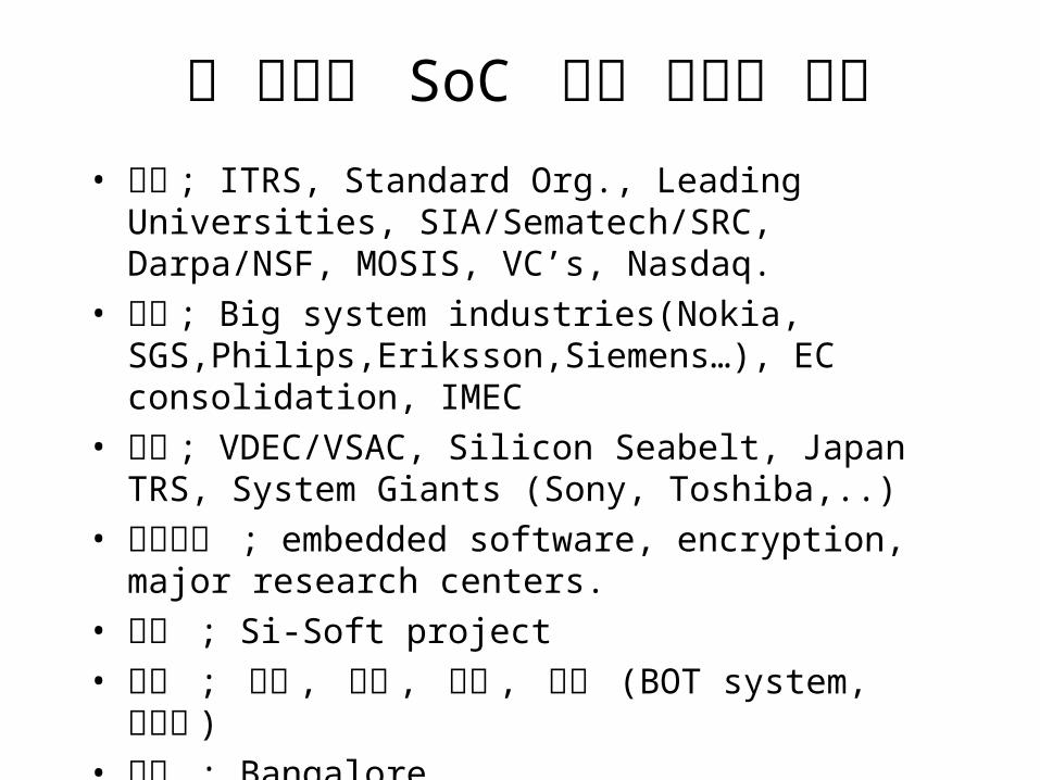
각 나라의 SoC 개발 전략과 현황• 미국 ; ITRS, Standard Org., Leading
Universities, SIA/Sematech/SRC, Darpa/NSF, MOSIS, VC’s, Nasdaq.
• 유럽 ; Big system industries(Nokia, SGS,Philips,Eriksson,Siemens…), EC consolidation, IMEC
• 일본 ; VDEC/VSAC, Silicon Seabelt, Japan TRS, System Giants (Sony, Toshiba,..)
• 이스라엘 ; embedded software, encryption, major research centers.
• 대만 ; Si-Soft project• 중국 ; 상해 , 심천 , 광주 , 북경 (BOT system,
국립대 )• 인도 ; Bangalore
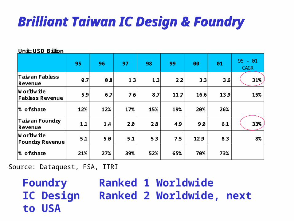
Brilliant Taiwan IC Design & FoundryBrilliant Taiwan IC Design & Foundry
Unit: USD Billion
95 96 97 98 99 00 01 95 - 01CAGR
Taiwan FablessRevenue
0.7 0.8 1.3 1.3 2.2 3.3 3.6 31%
WorldwideFabless Revenue
5.9 6.7 7.6 8.7 11.7 16.6 13.9 15%
% of share 12% 12% 17% 15% 19% 20% 26%
Taiwan FoundryRevenue
1.1 1.4 2.0 2.8 4.9 9.0 6.1 33%
WorldwideFoundry Revenue
5.1 5.0 5.1 5.3 7.5 12.9 8.3 8%
% of share 21% 27% 39% 52% 65% 70% 73%
Source: Dataquest, FSA, ITRI
Foundry Ranked 1 WorldwideIC Design Ranked 2 Worldwide, next to USA
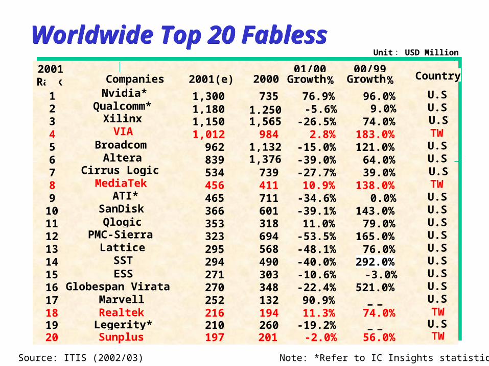
Worldwide Top 20 FablessWorldwide Top 20 Fabless
Source: ITIS (2002/03) Note: *Refer to IC Insights statistics
Unit : USD Million
2001Rank 2001(e) 2000
01/00 00/99Growth% Growth%
123456789
10111213141516171819
1,180 -5.6% 9.0%1,2501,150 -26.5% 74.0%1,5651,012 2.8% 183.0%984
962 -15.0% 121.0%1,132839 -39.0% 64.0%1,376534 -27.7% 39.0%739456 10.9% 138.0%411465 -34.6% 0.0%711366 -39.1% 143.0%601353 11.0% 79.0%318323 -53.5% 165.0%694295 -48.1% 76.0%568294 -40.0% 292.0%490271 -10.6% -3.0%303270 -22.4% 521.0%348252 90.9% --132216 11.3% 74.0%194210 260 -19.2% --
20
1,300 76.9% 96.0%735
CompaniesNvidia*
Qualcomm*Xilinx
VIABroadcom
AlteraCirrus Logic
MediaTekATI*
SanDiskQlogic
PMC-SierraLattice
SSTESS
Globespan VirataMarvellRealtekLegerity*Sunplus 197 201 -2.0% 56.0%
U.SU.SU.STWU.SU.SU.STWU.SU.SU.SU.SU.SU.SU.SU.SU.STWU.STW
Country
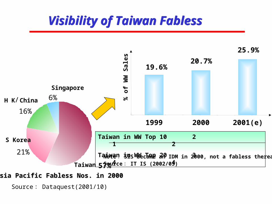
S Korea
21%
H K / China
16%
Singapore
6%
Taiwan 57%
Visibility of Taiwan FablessVisibility of Taiwan Fabless
Asia Pacific Fabless Nos. in 2000Asia Pacific Fabless Nos. in 2000
Source : Dataquest(2001/10)
Note : SiS became an IDM in 2000, not a fabless thereafterSource : IT IS (2002/03)
19.6%20.7%
25.9%
1999 2000 2001(e)%
of
WW
Sal
es
Taiwan in WW Top 10 2 1 2
Taiwan in WW Top 20 3 4 4
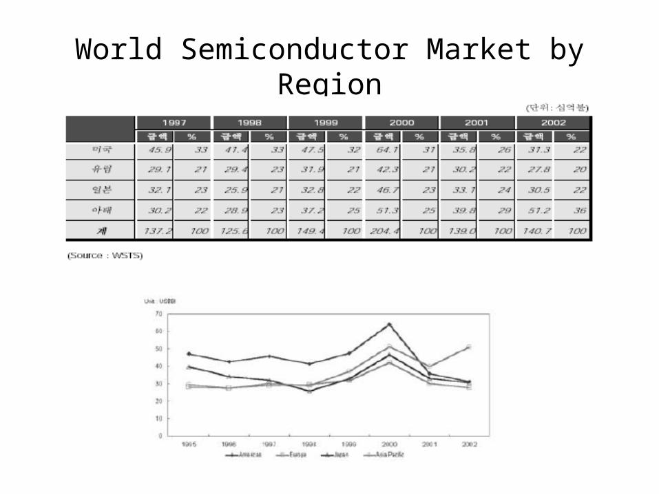
World Semiconductor Market by Region

World Semi Market by Application
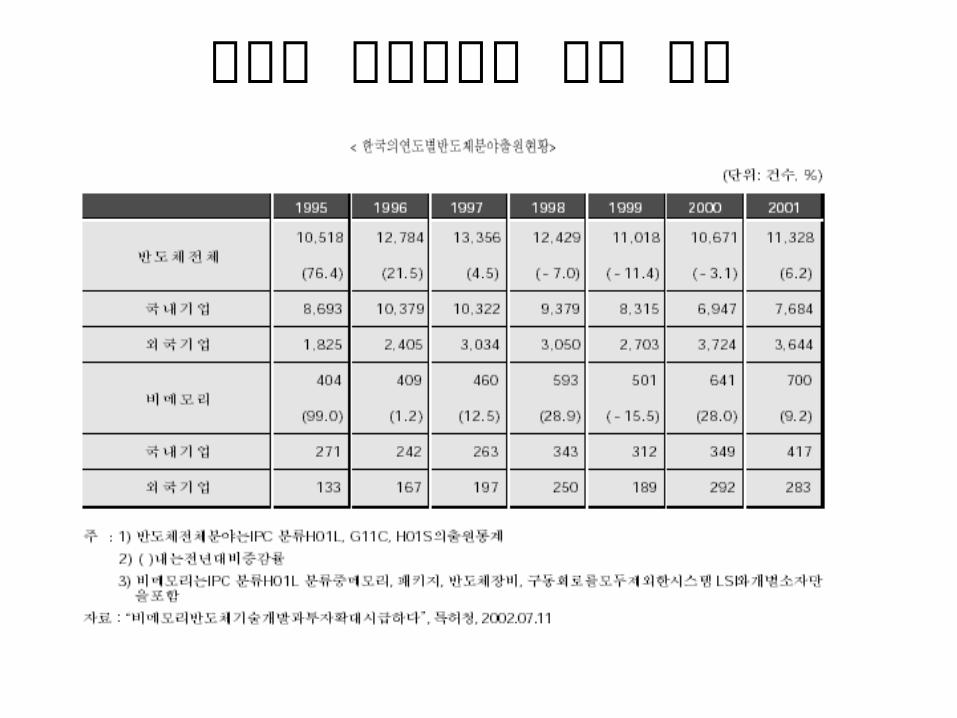
한국내 반도체특허 출원 현황
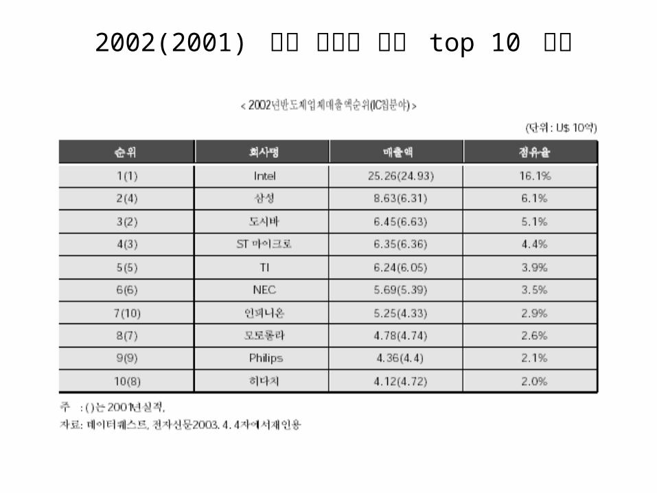
2002(2001) 세계 반도체 매출 top 10 기업
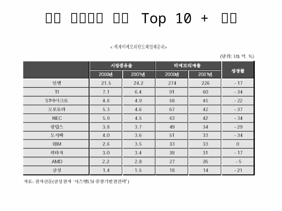
세계 비메모리 매출 Top 10 + 삼성
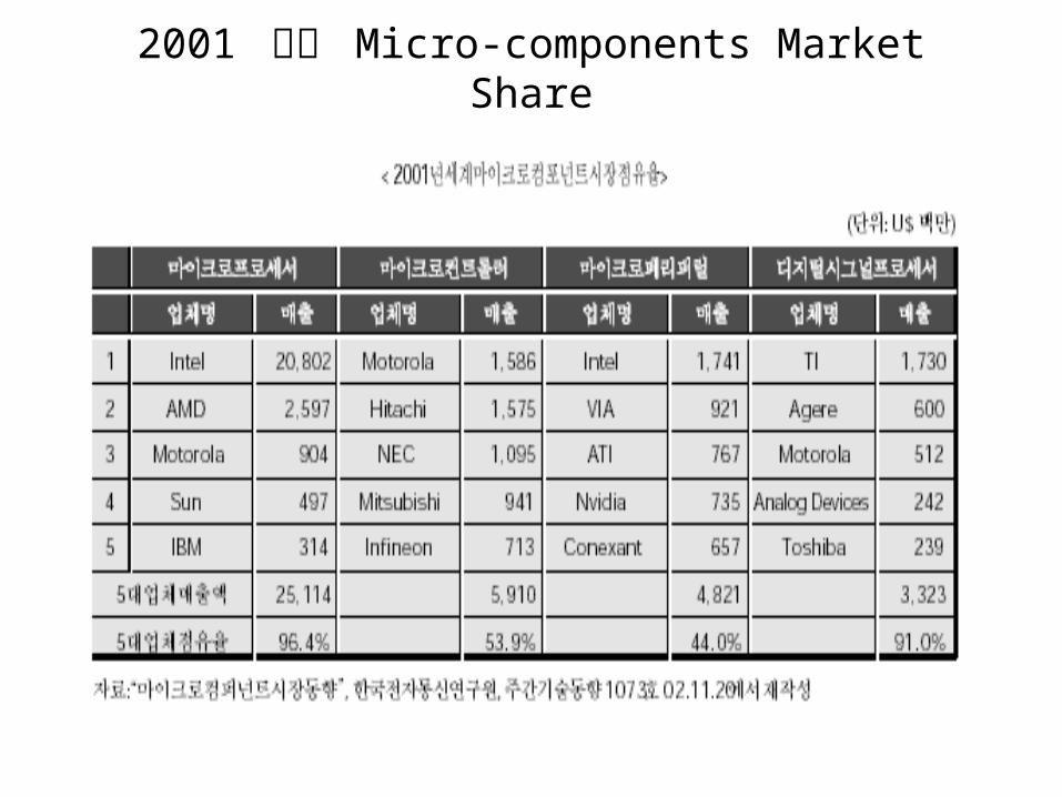
2001 세계 Micro-components Market Share
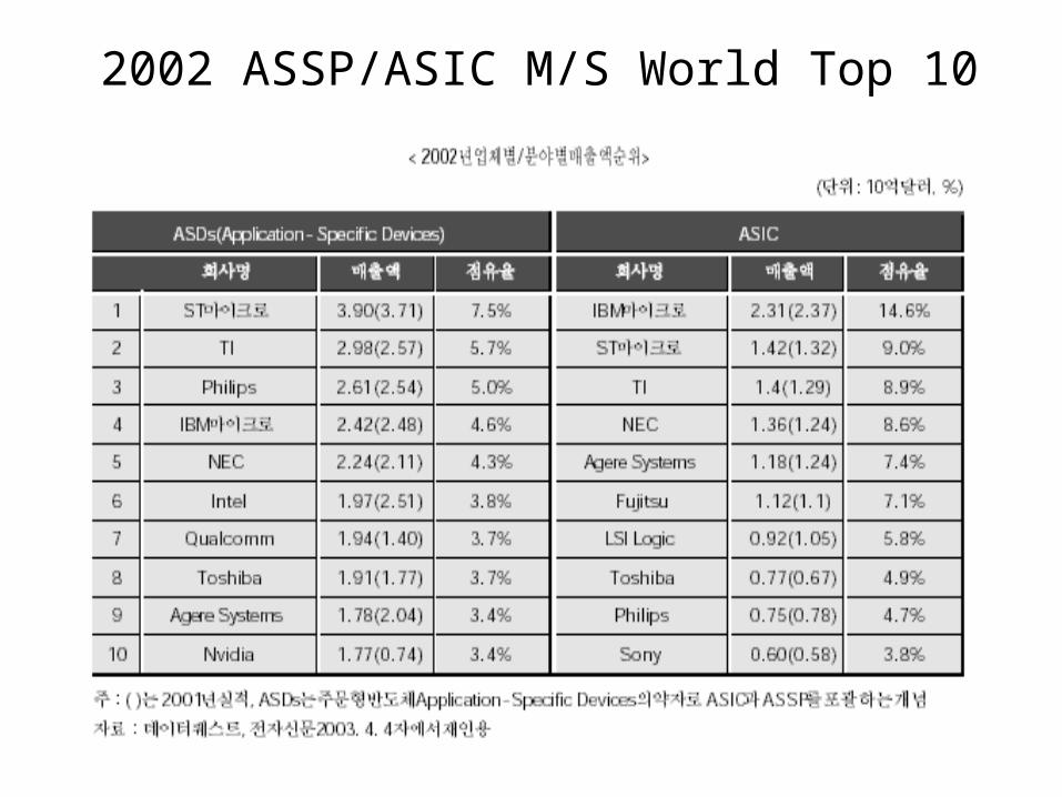
2002 ASSP/ASIC M/S World Top 10
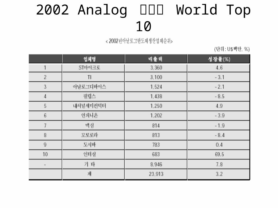
2002 Analog 반도체 World Top 10
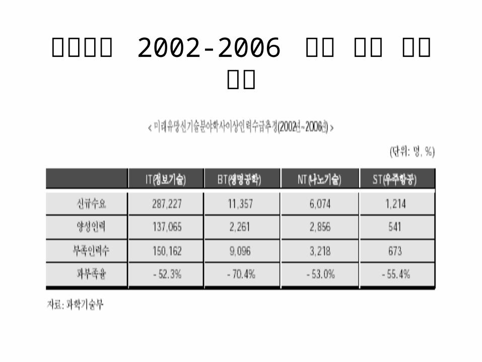
우리나라 2002-2006 학사 이상 인력 수요
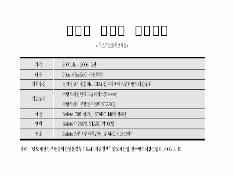
일본의 아스카 프로젝트

일본의 ASPLA Project
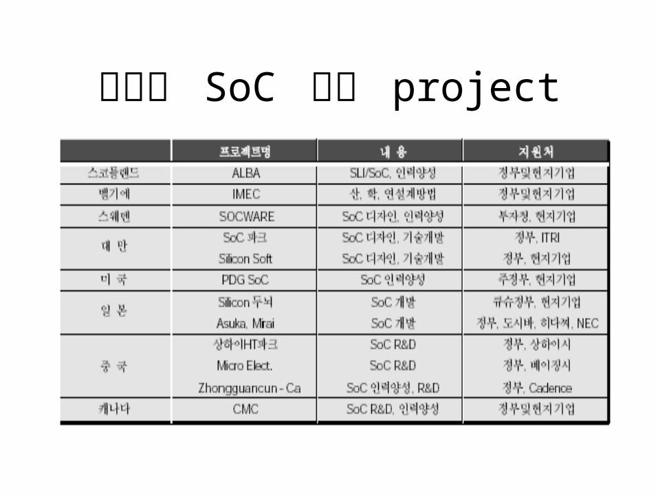
각국의 SoC 관련 project
Major Issues/Challenges of
SoC

SoC 가 가져오는 기회• 고속 성장하는 consumer product 의 특징은
portable, 저전력 소모 , 짧은 TTM (Time-to-Market) 임 .
• 이외에도 medical/bio/health, smart home, intelligent building, automotive/vehicle (최신 BMW 에는 processor core 가 1000 개 내장됨 ), military 시장에서도 SoC 의 엄청난 기능 /가격비 , 성능 /전력비는 새 응용을 열고 있다 .– 사람의 수명이 길어지고 , 출산율은 줄므로 생명과 복
지 , 교육 시장이 커 진다 .
SoC 가 가져오는 기회
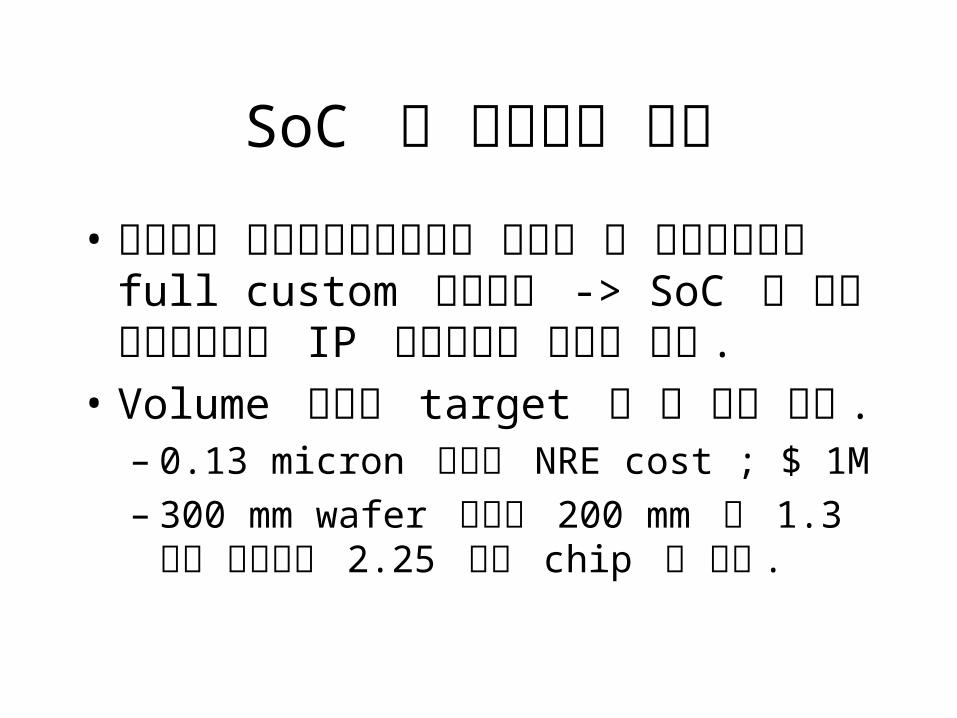
• 메모리와 마이크로프로세서가 견인해 온 반도체공정과 full custom 설계기술 -> SoC 에 의한 시스템설계와 IP 활용기술이 시장을 주도 .
• Volume 시장을 target 할 수 밖에 없음 .– 0.13 micron 공정의 NRE cost ; $ 1M– 300 mm wafer 공정은 200 mm 의 1.3
배의 비용으로 2.25 배의 chip 을 얻음 .
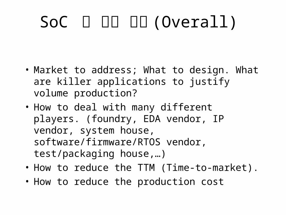
SoC 가 주는 도전 (Overall)
• Market to address; What to design. What are killer applications to justify volume production?
• How to deal with many different players. (foundry, EDA vendor, IP vendor, system house, software/firmware/RTOS vendor, test/packaging house,…)
• How to reduce the TTM (Time-to-market).• How to reduce the production cost
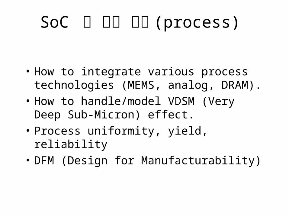
SoC 가 주는 도전 (process)
• How to integrate various process technologies (MEMS, analog, DRAM).
• How to handle/model VDSM (Very Deep Sub-Micron) effect.
• Process uniformity, yield, reliability• DFM (Design for Manufacturability)
한국의 SoC 설계기술의 발전 전략
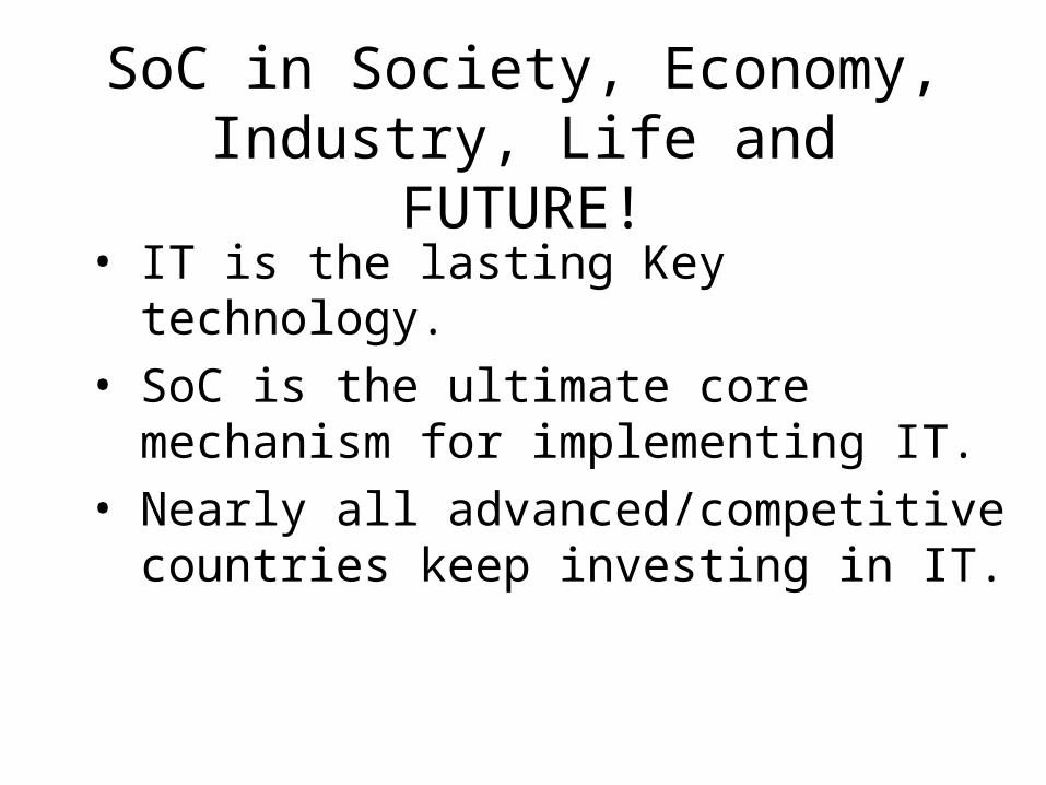
SoC in Society, Economy, Industry, Life and FUTURE!
• IT is the lasting Key technology.• SoC is the ultimate core mechanism
for implementing IT.• Nearly all advanced/competitive
countries keep investing in IT.
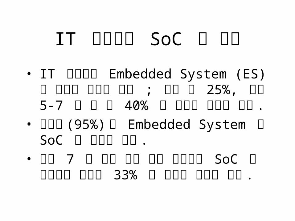
IT 산업에서 SoC 의 비중
• IT 산업에서 Embedded System (ES) 의 역할과 비중의 증대 ; 현재 약 25%, 향후 5-7 년 후 약 40% 에 접근할 것으로 보임 .
• 대부분 (95%) 의 Embedded System 은 SoC 로 구현될 것임 .
• 향후 7 년 후에 우리 나라 경제에서 SoC 가 차지하는 비중은 33% 에 육박할 것으로 보임 .
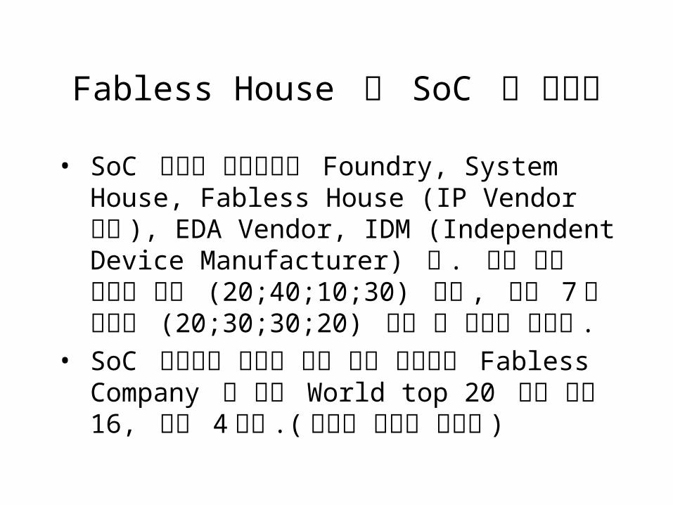
Fabless House 가 SoC 의 승부처
• SoC 산업의 구성요소는 Foundry, System House, Fabless House (IP Vendor 포함 ), EDA Vendor, IDM (Independent Device Manufacturer) 임 . 현재 시장 규모는 대략 (20;40;10;30) 이나 , 향후 7 년 후에는 (20;30;30;20) 으로 될 것으로 전망함 .
• SoC 산업분야 중에서 가장 빨리 성장하는 Fabless Company 의 경우 World top 20 내에 미국 16, 대만 4 개임 .( 한국도 일본도 전무함 )
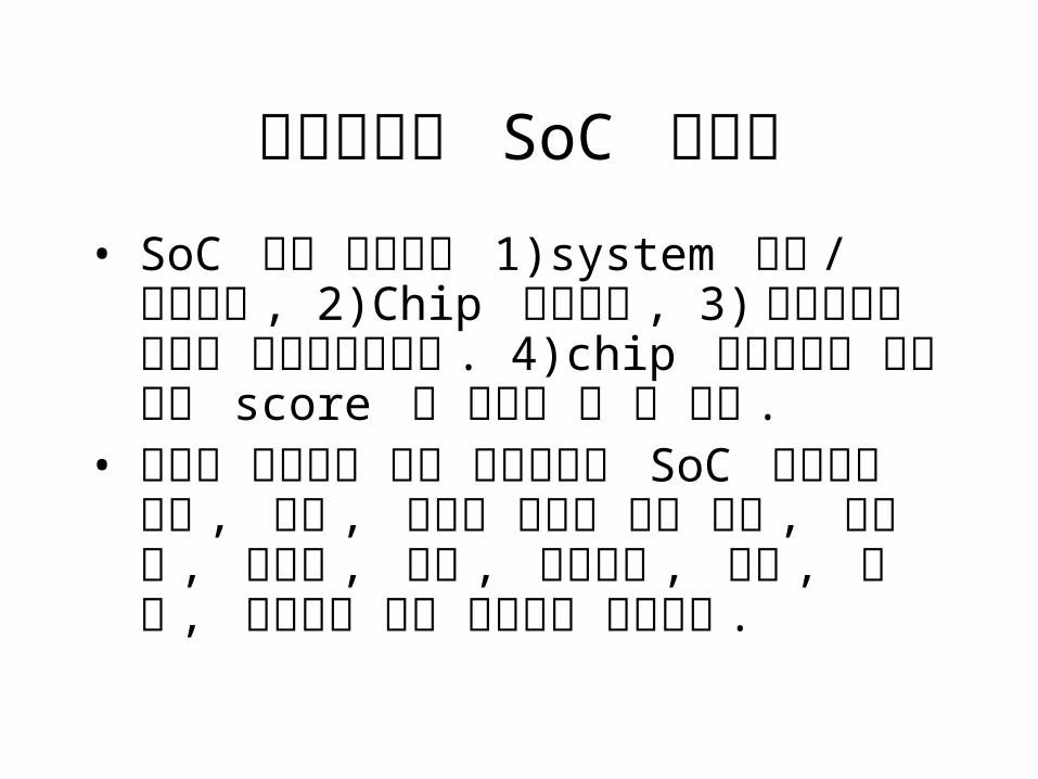
우리나라의 SoC 경쟁력
• SoC 국가 경쟁력은 1)system 착상 /설계능력 , 2)Chip 설계능력 , 3)내수시장의 크기와 국제마케팅능력 . 4)chip 제조기술에 대한 종합 score 로 평가해 볼 수 있다 .
• 이러한 기준에서 지금 우리나라의 SoC 경쟁력은 미국 , 일본 , 대만에 확실히 뒤져 있고 , 캐나다 , 프랑스 , 독일 , 이탈리아 , 중국 , 영국 , 이스라엘 등과 경쟁하는 입장이다 .
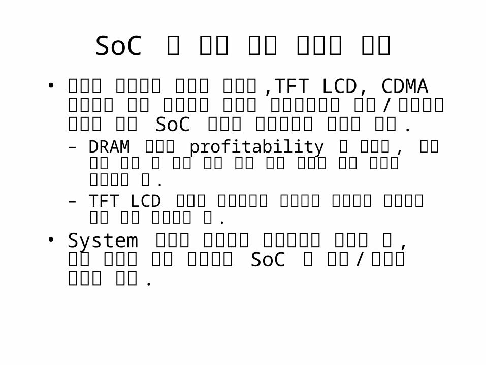
SoC 에 대한 우리 나라의 입장• 중국등 경쟁국에 대하여 반도체 ,TFT LCD,
CDMA 단말기등 일부 산업에서 가지는 경쟁력차이를 유지 /확장하는 유일한 길은 SoC 사업을 활성화하는 길밖에 없음 .– DRAM 산업은 profitability 뿐 아니라 , 돈을
번다 해도 번 돈을 거의 모두 계속 차세대 공장 건설에 투자해야 함 .
– TFT LCD 산업은 자본집약적 산업으로 언제든지 경쟁국에 추월 당할 가능성이 큼 .
• System 산업의 경쟁력과 부가가치를 높이는 길 , 역시 시스템 내에 내장되는 SoC 의 가치 /비중을 높이는 것임 .
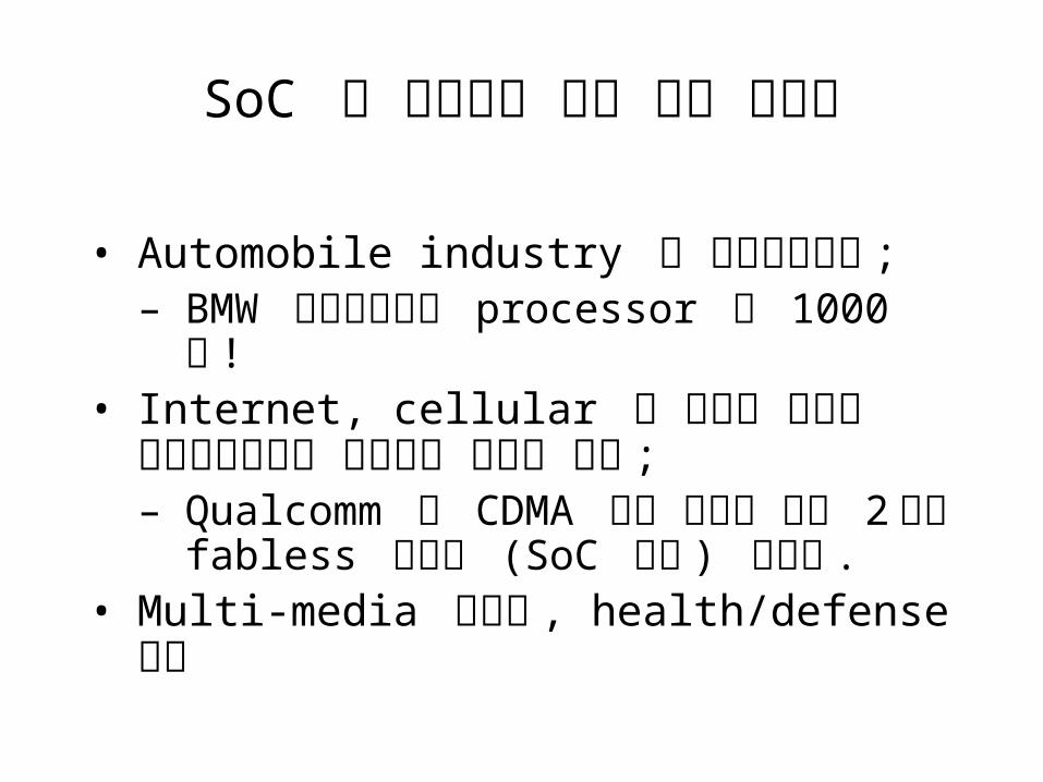
SoC 가 우리에게 주는 기회 요인들
• Automobile industry 의 고부가가치화 ;– BMW 최신기종에는 processor 가 1000
개 !• Internet, cellular 등 거대한 국내외
통신시장에서의 지속적인 성장의 기회 ;– Qualcomm 은 CDMA 기술 하나로 세계
2 위의 fabless 반도체 (SoC 설계 ) 회사임 .
• Multi-media 단말기 , health/defense 시장
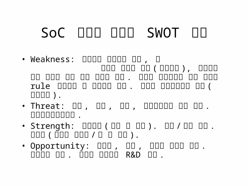
SoC 관점의 한국의 SWOT 분석
• Weakness: 다양성을 다루는데 약함 , 즉 분야간 /기능간 협력 ( 학제적 ) 마인드 부족 경청과 협상력 부족( 배달민족 ), 체계적인 개념 정립과 깊은 사고 훈련이 약함 . 개인의 능력과시를 전체 시스템 rule 준수보다 더 중요하게 여김 . 영어와 세계시민감각 부족 ( 유아독존 ). 질보다 양 , 내용보다 형식 우선주의 , 근시안적 사고
• Threat: 중국 , 인도 , 대만 , 선진제국과의 경쟁 심화 . 이공계기피심화현상 .
• Strength: 도전정신 ( 이길 수 있다 ). 향학 /성취 열정 . 자신감 ( 우리는 해냈다 /할 수 있다 ).
• Opportunity: 반도체 , 통신 , 자동차 산업의 존재 . 내수시장 있음 . 정부의 과학기술 R&D 투자 .
직업의 선택
1) 선택 시 고려할 점
• 나의 기술적 취향 /능력과
사회의 수요와 여건을 잘 살피라 .
• 분야는 전문적 적성 /능력으로 ,
직업 ( 연구 ,판매 , 관리 , 교육 , 중
재… ) 은 일반적 적성 /능력으로 선택 .
( 직업 /분야 /직장 /경력 ) 의 선택
2) 직업의 선택– 내가 좋아하고 , 보람을 느끼고 , 잘 할 수 있는 것 (educate,
research, develop, marketing & sales, policy, …)
– 내가 필요한 것을 제공해 주는 것 ( 자유 , 돈 , 명예 , 권한… )
– 유행 따라 , 가족의 강요에 따라 , 일시적 충동 ( 경쟁의식 , 감
정 , 욕심 ) 따라 하지 말 것 .
– 그 직업에 필요한데 내가 부족한 것은 계획성 있게 보완해 갈 것 .
(No one is perfect from the beginning.)
( 직업 /분야 /직장 /경력 ) 의 선택
3) 분야의 선택
– 내가 배운 기술 /지식이 효과적으로 적용되는 분야 (
기투자 분의 효용성 )
– 내가 앞으로 재미있게 해 나갈 수 있는 분야 ( 실력과
관심 )
– 사회의 수요 , 시장과 기술의 발전 추세를 고려
– Career plan 과 연계 ( 도달할 탁월의 수준과 활용방안 )
( 직업 /분야 /직장 /경력 ) 의 선택
4) 직장의 선택
– 명확한 목표가 있고 윤리적이고 우수한 ( 기술 or
비기술 ) 사람들이 있는 직장 .
– 내가 가치 있는 공헌을 할 수 있는 곳 ( 내가 그들을
행복하게 해 줄 수 있나 ?)
– 적어도 5년은 옮기지 않도록 하라 .
– 조국을 생각하라 .( 적어도 조국이 살도록 , 조국을
통하여 세계가 행복하도록 처신하라 .)
( 직업 /분야 /직장 /경력 ) 의 선택
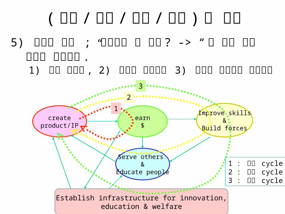
5) 경력의 선택 ; 공부해서 남 주냐 ? -> “남 주기 위해 죽도록 공부하라 .”
1) 남을 돕거나 , 2) 사람을 키우거나 3) 이러한 인프라를 만들거나
( 직업 /분야 /직장 /경력 ) 의 선택
createproduct/IP
earn$
Improve skills&
Build forces
Serve others &
Educate people
Establish infrastructure for innovation,education & welfare
1 : 자선 cycle2 : 교육 cycle3 : 정치 cycle
1
2
3

어떤 사람을 어떻게 키울 것이냐 ?
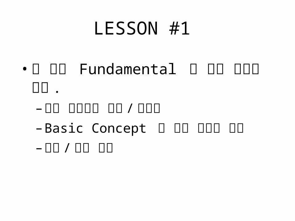
LESSON #1
• 세 가지 Fundamental 이 강한 사람이 필요 .– 깊이 생각하는 능력 /추진력– Basic Concept 에 대한 확실한 이해– 대화 /협동 능력
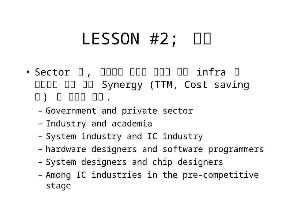
LESSON #2; 연결
• Sector 간 , 분야간의 교류와 협력을 위한 infra 를 구축하고 이를 통해 Synergy (TTM, Cost saving 등 ) 를 올려야 한다 . – Government and private sector– Industry and academia– System industry and IC industry– hardware designers and software programmers– System designers and chip designers– Among IC industries in the pre-competitive
stage
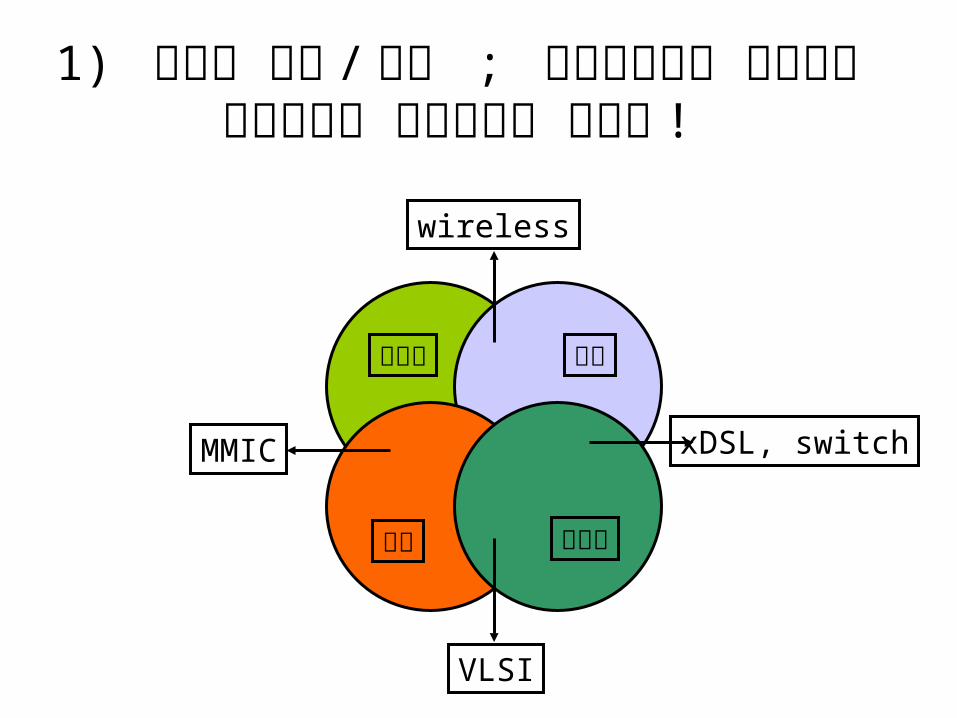
1) 개인의 경력 /전공 ; 주력분야에서 탁월하고 인접분야와 연결고리가 있어야 !
회로
전자기 통신
반도체
VLSI
MMIC xDSL, switch
wireless
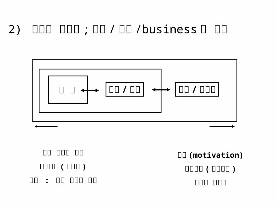
2) 국가의 경쟁력 ;교육 /연구 /business 의 연결
교 육 연구 / 개발 창업 / 상품화
실력 향상의 효율
핵심기술 ( 돌파력 )
지식 : 고속 단방향 흐름
동기 (motivation)
응용기술 ( 대응능력 )
다자간 쌍방향

3) 기업의 경쟁력 ; 기술과 비기술의 연결
지원조
Base Camp
특허전략경영
투자유치제휴 ,M&A
시장심리기술표준
.
.
.
정상 공격조
Top of mountain
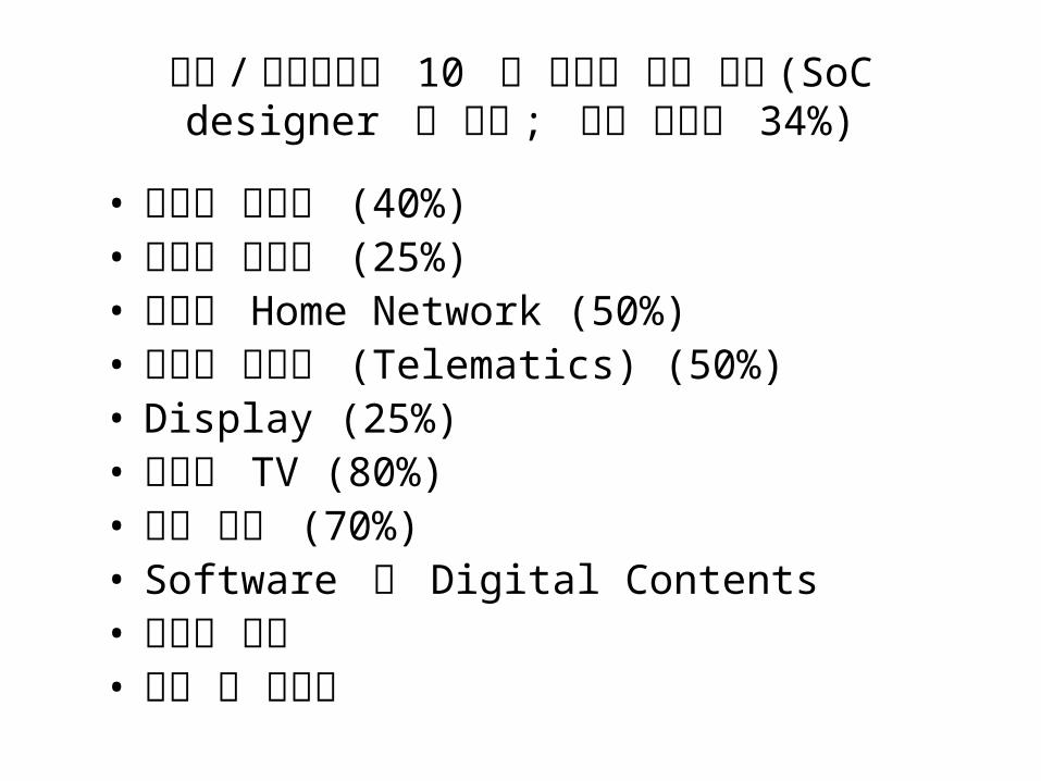
한국 /참여정부의 10 대 신성장 동력 산업(SoC designer 의 비중 ; 전체 산업의 34%)
• 차세대 반도체 (40%)• 지능형 로보트 (25%)• 지능형 Home Network (50%)• 미래형 자동차 (Telematics) (50%)• Display (25%)• 디지털 TV (80%)• 이동 통신 (70%)• Software 및 Digital Contents • 차세대 전지• 신약 및 바이오
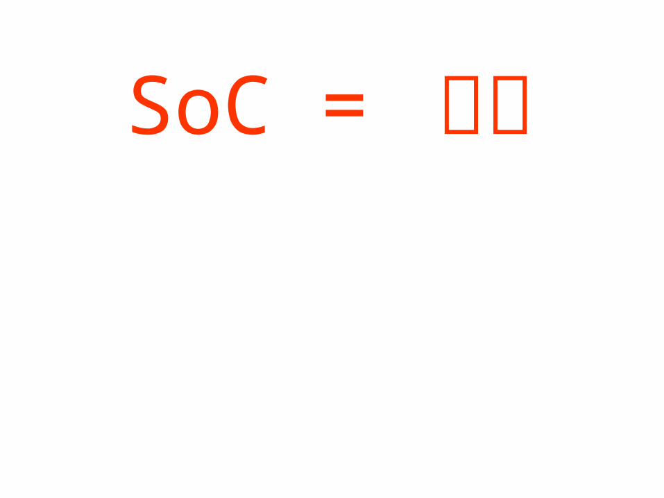
SoC = 기회SOC : System 과 Chip 을
연결함으로써 생기는 Opportunity