various topics related to feb liang han, ge jin university of science and technology of china...
TRANSCRIPT
Various Topics Related to FEB
Liang Han, Ge JinUniversity of Science and Technology of China
Dec.21,2013
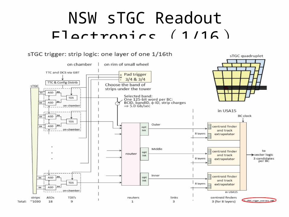
NSW sTGC Readout Electronics( 1/16)

FE Boards
V. Polychronakos Muon Week 16-20 September 2013 3
Two kinds of FE boards:
128 channel for PAD and Wires, Total of FE boards for Pad and wires: 2416 2=768
512 channel for strips, Total of FE Boards for strip: 2416 2=768
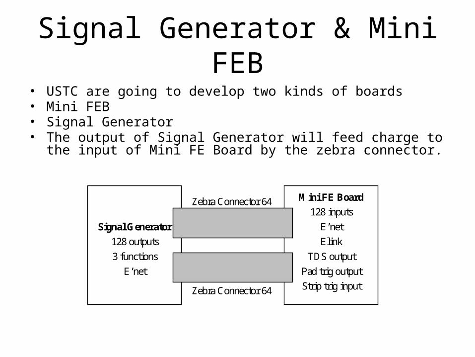
Signal Generator & Mini FEB• USTC are going to develop two kinds of boards• Mini FEB• Signal Generator• The output of Signal Generator will feed charge to the input of Mini FE
Board by the zebra connector.
Zebra Connector 64
Zebra Connector 64
Signal Generator
128 outputs
3 functions
E’net
Mini FE Board
128 inputs
E’net
Elink
TDS output
Pad trig output
Strip trig input

Functions of Signal GeneratorFunctions:.1) Same signals for all output;
2) Random signals to simulate TGC strip output;
3) 64 strip output + 64 pad output
USTC 5
Zebra Conn 64Zebra Conn 64
FPGAXC6VLX240T
Driver
strip0
strip63
strip64
strip128
To FEB

Mini FE Board
USTC 6
Zebra Conn 64Zebra Conn 64
VMM2
VMM2
FPGAXC6VLX240T
Strip0
Strip64
Strip128
Strip63
Ethernet
Strip trig in
Pad trig
E-Link
PC
GBT
in
At first Ethernet will be used to read out data and configure VMM
Then develop E-link firmware to connect GBT
out
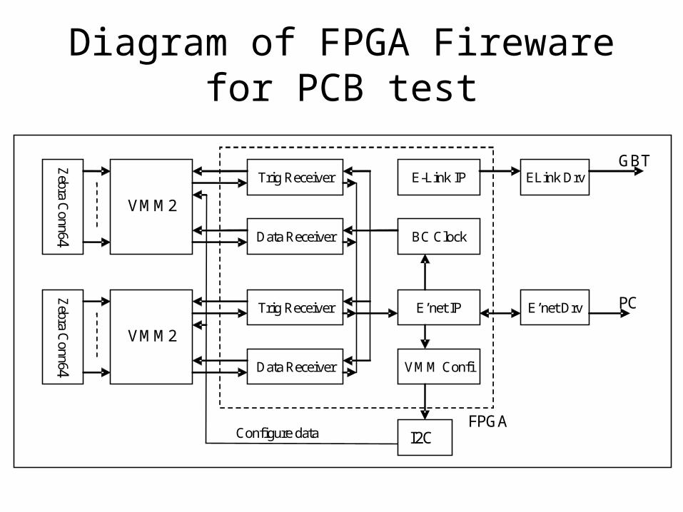
Diagram of FPGA Fireware for PCB test
FPGA
GBT
PC
Configure data
Zebra C
onn64 Z
ebra Conn64
VMM2
VMM2
Trig Receiver
Trig Receiver
Data Receiver
Data Receiver
E’net IP
E-Link IP
BC Clock
VMM Confi
E’net Drv
ELink Drv
I2C

Diagram of FPGA firmware for TDS test
Pad trigger in
Pad trigger out
GBT
PC
Configure data
Zebra C
onn64 Z
ebra Conn64
VMM2
VMM2
Trig Receiver
Trig Receiver
Pad TDS
Strip TDS
E’net IP
E-Link IP
BC Clock
VMM Confi
E’net Drv
FPGA
ELink Drv
I2C Drv
Serializer

Purposes of Development of Mini FEB
FEB PCB Test1. Analog performances of PCB: impedance of input, matching, shape of
signal, noise on PCB, protection circuit, test input2. Zebra performances: type, size, resistance, capacitance, crosstalk,
mounting on PCB3. Power, GNDVMM Understanding4. Configuration of VMM, BC clock, TTC5. Read out data from VMM 6. Consistency and crosstalk between channelsTDS Emulation7. Pad trigger8. Strip trigger logic emulation
University of Science and Technology of China 9

Zebra Connector• Type?• Pitch number: for 64/128/512 channels?• Size: Height, length, width• How to mount zebra on PCB?• Vendor?• Crosstalk• Impedance, capacity: is it changed in different temperature?• Working life?• Absolute maximum ratings: voltage, temperature • How to feed in signal? 1 signal+1 ground per channel from
sTGC to VMM

Questions about VMM2• How many tests have been done for VMM1 • Protection circuit, if it is needed to design on PCB again?• Analog Input via zebra connector?• Matching in input stage?• What kinds of tests for VMM2 will be done in BNL?• Specification of VMM2• How to consider the pin map of VMM during designing VMM?• Output of VMM2 connect to V6 FPGA directly?• Grounding: analog GND and digital GND in VMM2, How to
deal with GND on PCB.• Differences between VMM2 and VMM3: func, size, package

Schedule of Mini FE Board
USTC 12

Thank You!

The Second version of the ASIC (VMM2)
nSW Electronics Workshop - V. Polychronakos, BNLIBM 8RF 130 nm CMOS process, 1.2 V 9.1 x 9.1 mm2, ~6.5 mW/channel
G. De Geronimo, BNL Instr. Div.• Fixes issues (mostly minor) of the first version• Includes 10-bit digitizers for amplitude and timing (200 ns)• Includes a 6-bit Amplitude digitizer at ~40 ns conversion
time• Includes 4 word buffer, simultaneous read/write, can
continuously be read out at both phases of 200 MHz clock in DDR mode 800 Mbps
11-12/11/2013 14
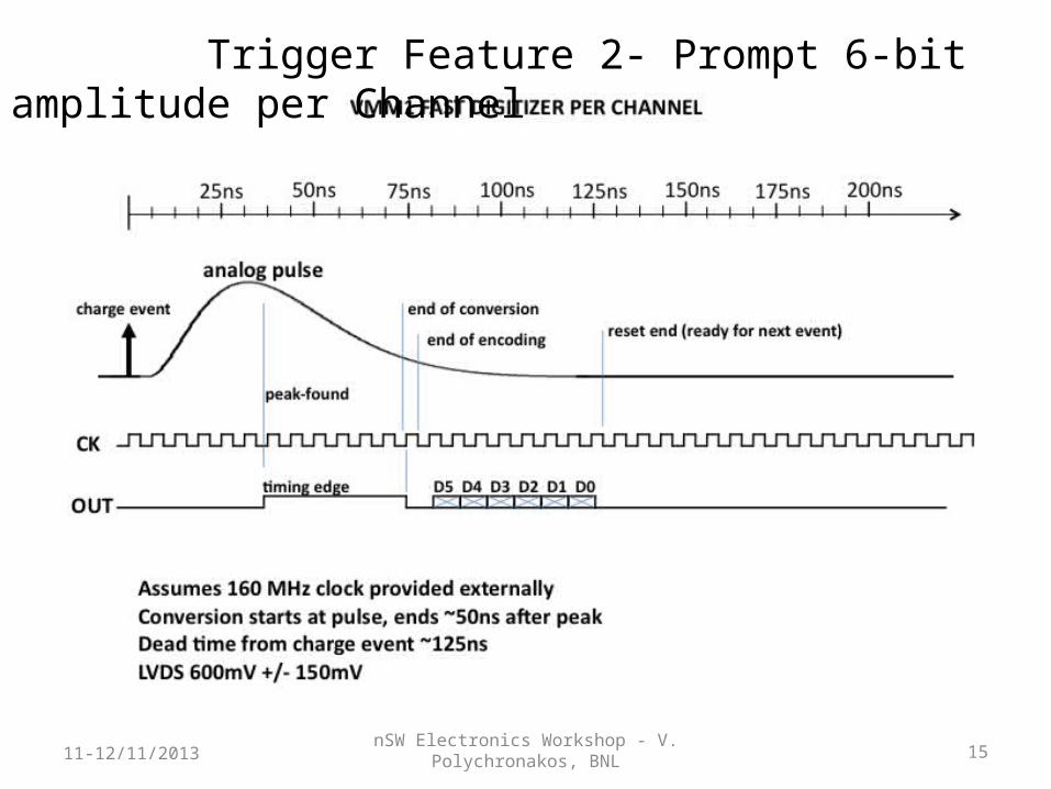
Trigger Feature 2- Prompt 6-bit amplitude per Channel
nSW Electronics Workshop - V. Polychronakos, BNL11-12/11/2013 15
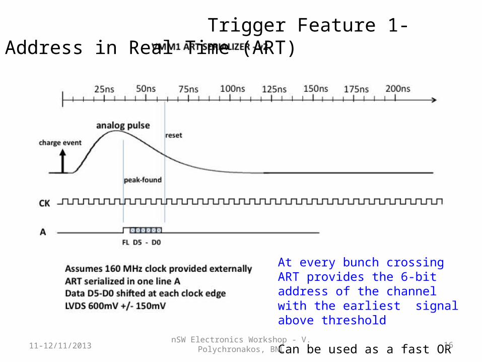
Trigger Feature 1- Address in Real Time (ART)
At every bunch crossing ART provides the 6-bit address of the channel with the earliest signal above threshold
Can be used as a fast OR
nSW Electronics Workshop - V. Polychronakos, BNL11-12/11/2013 16
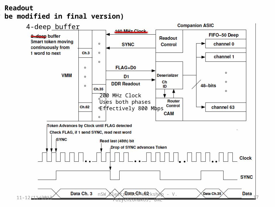
4-deep buffer
VMM2 Readout(May be modified in final version)
200 MHz ClockUses both phasesEffectively 800 Mbps
nSW Electronics Workshop - V. Polychronakos, BNL11-12/11/2013 17