vce vet · pdf filesection number of questions number of questions number of to be answered...
TRANSCRIPT

Figures
Words
STUDENT NUMBER Letter
VCE VET ELECTRONICS
Written examination
Structure of book
Friday 1 November 2002
Reading time: 3.00 pm to 3.15 pm (15 minutes)Writing time: 3.15 pm to 4.45 pm (1 hour 30 minutes)
QUESTION AND ANSWER BOOK
• Students are permitted to bring into the examination room: pens, pencils, highlighters, erasers,sharpeners, rulers, an approved graphics calculator (memory cleared) and/or one scientific calculator.
• Students are NOT permitted to bring into the examination room: blank sheets of paper and/or white outliquid/tape.
Materials supplied• Question and answer book of 21 pages including a formula sheet for Sections 1, 2 and 3 on page 21.
Instructions• Write your student number in the space provided above on this page.• Answer all questions in the spaces provided in this book.• Note: There are no separate items for Mathematics for Electronics 2. Understanding of mathematics has
been incorporated into the questions in Sections 1–3.• State all formulas and calculations.• All units must be specified in the answers.
• All written responses must be in English.
SUPERVISOR TO ATTACH PROCESSING LABEL HERE
Section Number of questions Number of questions Number ofto be answered marks
1 – DC power supplies 7 7 412 – Analogue systems 8 8 223 – Digital electronics 1 and Digital 8 8 35
and computer systemsTotal 98
Victorian Certificate of Education2002
VICTORIAN CURRICULUM AND ASSESSMENT AUTHORITY 2002
Students are NOT permitted to bring mobile phones and/or any other electronic communicationdevices into the examination room.

VCE VET ELECTRONICS 2
SECTION 1 – DC power supplies
Question 1
Switched Mode Power Supplies are used as power supplies for modern electronic equipment such as laptopcomputers and mobile phones.
The Switched Mode Power Supply is used in preference to a conventional power supply because
A. it is more efficient.
B. it is more compact.
C. it can be designed for varying levels of AC input voltages.
D. All of the above.
1 mark
Question 2
Simple voltage regulation can be achieved by using a Zener diode.
When used in a circuit, a Zener diode is always
A. reverse biased.
B. connected in series.
C. troubled by overheating.
D. forward biased.
1 mark
Question 3
A typical conventional DC power supply is shown in Figure 1 below.
Figure 1
The four stages of the circuit can be represented as a block diagram as shown in Figure 2 below.
Figure 2SECTION 1 – Question 3 – continued
C1+
A
B
18 VRMS240 VAC50 Hz
IC1
7812
2200 µ
Load
C
D
E
F
F
transformer rectifier filter voltageregulator
ACinput

3 VCE VET ELECTRONICS
SECTION 1 – continuedTURN OVER
Explain the function of each of the following components of the circuit in Figure 1.
i. Transformer
ii. Rectifier
iii. Filter
iv. Voltage regulator
4 × 2 = 8 marks
VCE VET ELECTRONICS 4
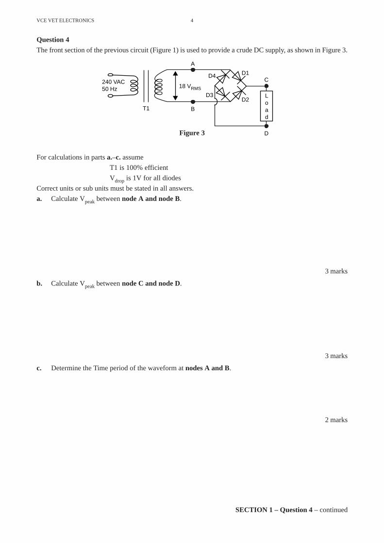
Question 4
The front section of the previous circuit (Figure 1) is used to provide a crude DC supply, as shown in Figure 3.
Figure 3
For calculations in parts a.–c. assume
T1 is 100% efficient
Vdrop is 1V for all diodes
Correct units or sub units must be stated in all answers.
a. Calculate Vpeak between node A and node B.
3 marks
b. Calculate Vpeak between node C and node D.
3 marks
c. Determine the Time period of the waveform at nodes A and B.
2 marks
SECTION 1 – Question 4 – continued
CD1
T1
D2
D4
D3
A
D
B
18 VRMS240 VAC50 Hz
Load

5 VCE VET ELECTRONICS
SECTION 1 – Question 4 – continuedTURN OVER
d. On the axes provided below, sketch the output waveform that would be observed between nodes A and B.
Show at least one full cycle of the waveform using the correct timeline, and the peak voltage.
Figure 4
3 marks
e. In Figures 5 and 6 below, clearly draw in arrows showing the conventional current path through the diodesand the load during each cycle of rectification.
Use Figure 5 for the first half cycle and Figure 6 for the second half cycle.
First half cycle Second half cycle
Figure 5 Figure 6
2 marks
–5
05 10 15 20 25 30 35 40 45 50
–10
–15
–20
–25
–30
–35
5
10
15
20
25
30
35
v(volts)
t (ms)
C
D1
D2
D4
D3
A
D
B
18 VRMS
Load
C
D1
D2
D4
D3
A
D
B
18 VRMS
Load
VCE VET ELECTRONICS 6
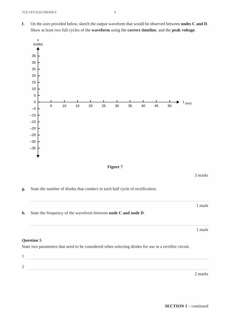
f. On the axes provided below, sketch the output waveform that would be observed between nodes C and D.
Show at least two full cycles of the waveform using the correct timeline, and the peak voltage.
Figure 7
3 marks
g. State the number of diodes that conduct in each half cycle of rectification.
1 mark
h. State the frequency of the waveform between node C and node D.
1 mark
Question 5
State two parameters that need to be considered when selecting diodes for use in a rectifier circuit.
1
2
2 marks
SECTION 1 – continued
–5
05 10 15 20 25 30 35 40 45 50
–10
–15
–20
–25
–30
–35
5
10
15
20
25
30
35
v(volts)
t (ms)
7 VCE VET ELECTRONICS
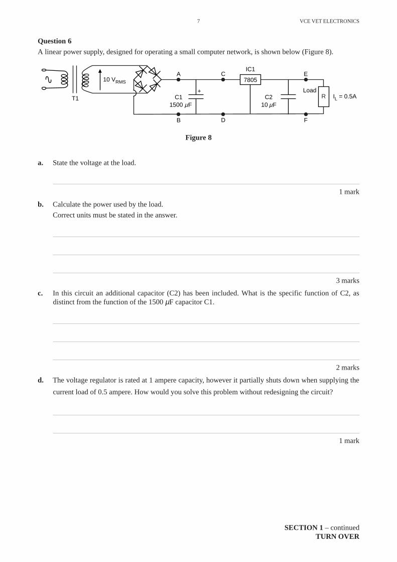
Question 6
A linear power supply, designed for operating a small computer network, is shown below (Figure 8).
Figure 8
a. State the voltage at the load.
1 mark
b. Calculate the power used by the load.
Correct units must be stated in the answer.
3 marks
c. In this circuit an additional capacitor (C2) has been included. What is the specific function of C2, asdistinct from the function of the 1500 µF capacitor C1.
2 marks
d. The voltage regulator is rated at 1 ampere capacity, however it partially shuts down when supplying the
current load of 0.5 ampere. How would you solve this problem without redesigning the circuit?
1 mark
SECTION 1 – continuedTURN OVER
IL = 0.5AC1+
A
B
10 VRMS
IC1
7805
1500 µC2 R
Load
C
D
E
F
F 10 µFT1
VCE VET ELECTRONICS 8
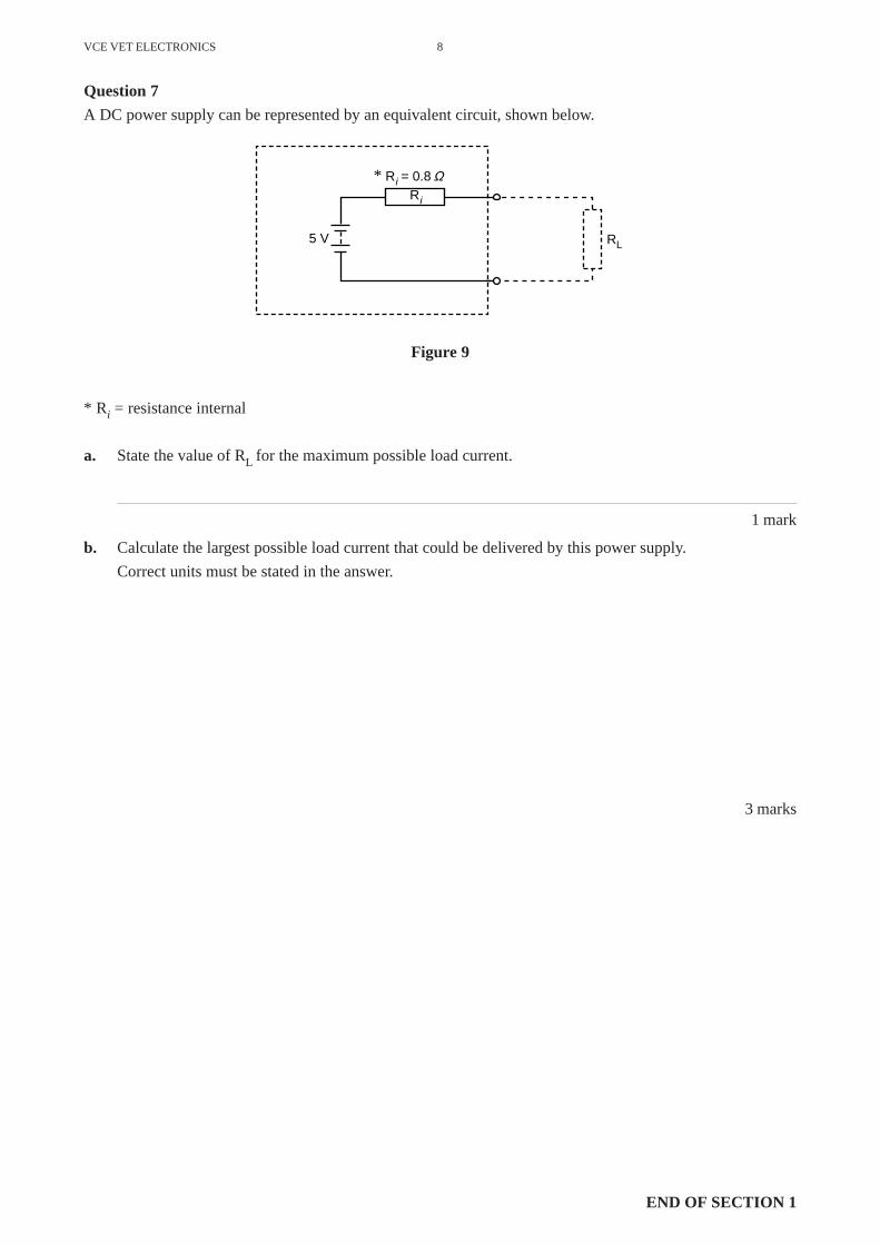
Question 7
A DC power supply can be represented by an equivalent circuit, shown below.
Figure 9
* Ri = resistance internal
a. State the value of RL for the maximum possible load current.
1 mark
b. Calculate the largest possible load current that could be delivered by this power supply.
Correct units must be stated in the answer.
3 marks
END OF SECTION 1
Ri
* Ri = 0.8
RL5 V
Ω
9 VCE VET ELECTRONICS
SECTION 2 – Analogue systems
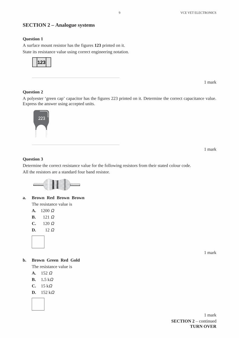
Question 1
A surface mount resistor has the figures 123 printed on it.
State its resistance value using correct engineering notation.
1 mark
Question 2
A polyester ‘green cap’ capacitor has the figures 223 printed on it. Determine the correct capacitance value.Express the answer using accepted units.
1 mark
Question 3
Determine the correct resistance value for the following resistors from their stated colour code.
All the resistors are a standard four band resistor.
a. Brown Red Brown Brown
The resistance value is
A. 1200 ΩB. 121 ΩC. 120 ΩD. 12 Ω
1 mark
b. Brown Green Red Gold
The resistance value is
A. 152 ΩB. 1.5 kΩC. 15 kΩD. 152 kΩ
1 markSECTION 2 – continued
TURN OVER
123

VCE VET ELECTRONICS 10
Question 4
A computer memory backup capacitor is 0.47 F.
Calculate the quantity of charge the capacitor will store when charged to 5 volts.
Correct units of charge must be stated.
3 marks
Question 5
Explain the process of energy conversion that takes place in a speaker whenan appropriate audio signal is applied to the inputs and sound is produced.
Detailed representation using block diagrams is acceptable.
3 marks
SECTION 2 – continued
A loudspeaker
11 VCE VET ELECTRONICS
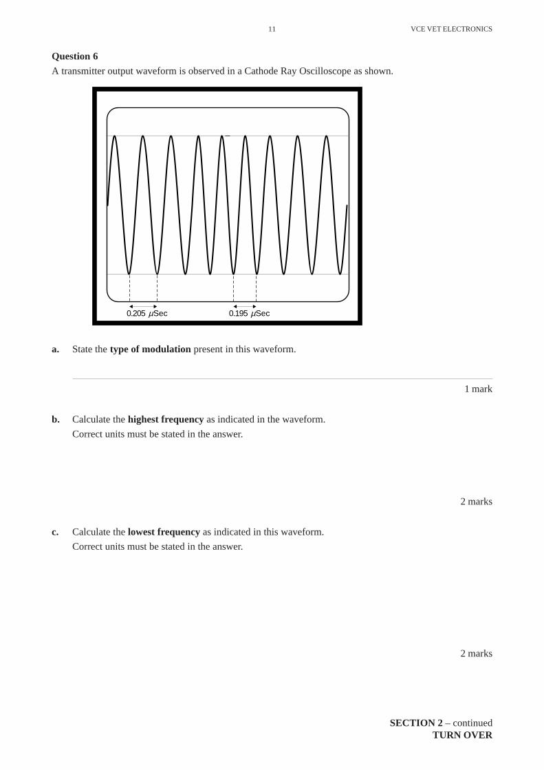
Question 6
A transmitter output waveform is observed in a Cathode Ray Oscilloscope as shown.
a. State the type of modulation present in this waveform.
1 mark
b. Calculate the highest frequency as indicated in the waveform.
Correct units must be stated in the answer.
2 marks
c. Calculate the lowest frequency as indicated in this waveform.
Correct units must be stated in the answer.
2 marks
SECTION 2 – continuedTURN OVER
Secµ0.205 Secµ0.195
VCE VET ELECTRONICS 12
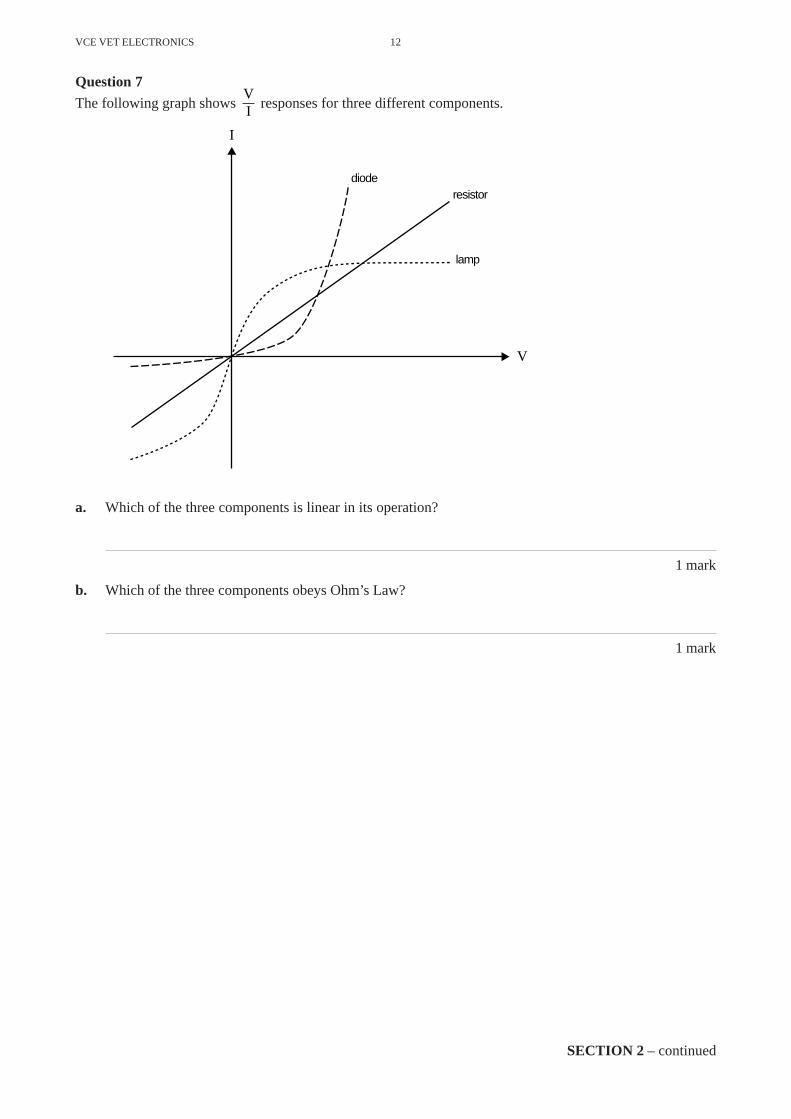
Question 7
The following graph shows VI responses for three different components.
a. Which of the three components is linear in its operation?
1 mark
b. Which of the three components obeys Ohm’s Law?
1 mark
SECTION 2 – continued
I
V
dioderesistor
lamp

13 VCE VET ELECTRONICS
Question 8Varying light can be used to control circuit operations when an LDR is utilised.
The characteristics of the LDR are shown in the graph below.
Figure 10
Figure 11
Referring to the circuit diagram above (Figure 11) determine the following.
a. What do the letters LDR represent?
1 mark
b. The component ‘Q1’ is identified as a
A. FET
B. SCR
C. PNP transistor
D. NPN transistor
1 mark
SECTION 2 – Question 8 – continuedTURN OVER
100 kΩ
100
dark bright light
light level
resistance
Ω
2 kΩ 1 kΩ
V supply
V out
0 volts
LDR
Q1
VCE VET ELECTRONICS 14
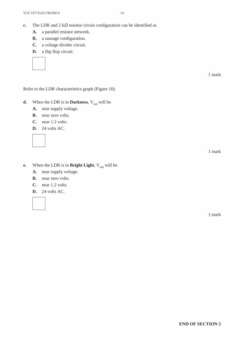
c. The LDR and 2 kΩ resistor circuit configuration can be identified as
A. a parallel resistor network.
B. a sausage configuration.
C. a voltage divider circuit.
D. a flip flop circuit.
1 mark
Refer to the LDR characteristics graph (Figure 10).
d. When the LDR is in Darkness, Vout will be
A. near supply voltage.
B. near zero volts.
C. near 1.2 volts.
D. 24 volts AC.
1 mark
e. When the LDR is in Bright Light , Vout will be
A. near supply voltage.
B. near zero volts.
C. near 1.2 volts.
D. 24 volts AC.
1 mark
END OF SECTION 2

15 VCE VET ELECTRONICS
SECTION 3 – Digital electronics 1 and Digital and computer systems
Question 1
The optical mouse is sometimes used instead of the conventional ball mouse on computers.
State one commonly recognised advantage the optical mouse has over a conventional mouse.
1 mark
Question 2
a. Within a Personal Computer System, the mouse is best described as
A. an output device
B. a parallel interface
C. a ROM
D. an input device
E. a clicker
1 mark
b. An older laptop computer, without a USB port, needs to be connected to a laser printer with a parallel port.
Select the most appropriate port on the laptop to use, from the available list.
A. LPT1
B. COM1
C. COM2
D. PS2
1 mark
SECTION 3 – continuedTURN OVER

VCE VET ELECTRONICS 16
Question 3
The circuit below (Figure 12) is a metal pipe locator circuit.
Figure 12
a. State the type of gates contained within the CD4001.
1 mark
b. State the logic function being performed by the gate IC1 a.
1 mark
c. Figure 12 shows two arrows indicating a connection to the IC pin 14 and IC pin 7. Explain the function ofthese connections.
2 marks
TO ICPIN 14
TO ICPIN 7
C2
C10.1 F
IC1 b
IC1 CD4001
IC1 a IC1 d
IC1 c
µ
C4.01 Fµ
C5.0047 Fµ
C3.001 Fµ
R515 Ω
C6100 F10VW
µ 9 voltbattery
MAGNETICEARPIECE
TR1DS548
R4
15 k
680 k
R2
R3
1.2 M
390 pF
RV14.7 k
6.8 k
L1
5
6
1
2
3
4 8
9
12
13
10
11
SECTION 3 – continued

17 VCE VET ELECTRONICS
Question 4
The diagram (Figure 13) shows an ‘Exclusive OR gate’ constructed from standard logic gates.
Figure 13
a. Complete the following truth table for the logic functions in Figure 13.
Table 1
5 marks
b. State the most simplified Boolean expression for Figure 13.
2 marks
c. Draw the single logic gate symbol that represents an XOR gate.
1 mark
B
0
0
1
1
0
1
0
1
A A B A.B A.B Q
BA
B
Q
A
A.B
A.B
SECTION 3 – continuedTURN OVER

VCE VET ELECTRONICS 18
Question 5
LCD (displays) require more complex circuitry to drive them compared to LED displays.
a. What do the letters LCD stand for?
1 mark
b. In portable electronic equipment, LED displays have progressively been replaced with LCDs. State theprincipal reason for this change.
2 marks
c. When being used in a circuit, state the input logic level required by a common anode seven-segmentLED display for segment illumination.
1 mark
SECTION 3 – continued

19 VCE VET ELECTRONICS
Question 6
Refer to the data sheet extract provided above.
There are three inputs specified in the table below.
For each input you are required to
• indicate illuminated display segments using ‘H’
• indicate non illuminated display segments using ‘L’
• indicate the final display showing, by shading the segments which are illuminated.
Place all answers in the table below.
6 marks
msb lsbDCBA
INPUTS DISPLAY SEGMENT
0101
a
i.
ii.
iii.
b c d e f g
FINAL DISPLAYSHOWING
(Shade illuminatedsegments)
Assume LT and BI/BROheld high
1001
Assume LT and BI/BROheld high
1111
Assume LT held low
SECTION 3 – continuedTURN OVER

VCE VET ELECTRONICS 20
Question 7
Complete the following number conversions.
Decimal Binary BCD
a.
79
Hexadecimal Binary Decimal
b.
A3
2 + 2 = 4 marks
Question 8
An analogue signal is converted to a digital output by the ADC.
a. Calculate how many possible 8 bit binary numbers are available to represent different analogue inputvoltage levels.
2 marks
b. If full scale input is 1.02 volts, calculate the smallest input voltage change which will be detected at thedigital output.
2 marks
msb lsb msb lsb
c. If the binary output changed from 1000 0000 to 1000 0100, calculate the input voltage change that hasoccurred.
2 marksSECTION 3 – continued
01
08
digitaloutputs
analogueinput
0 – 1.02 volts8 BitADC

21 VCE VET ELECTRONICS
END OF QUESTION AND ANSWER BOOK
V = IR IVR
=
V Vpeak RMS= 2
Q = C × V
fT
= 1T
1=f
P = V × Ι
∆ V input = ∆ output × voltage step
Formulas
voltage stepvoltage full scalenumber of steps
=