verilog manal
DESCRIPTION
experiments using verilog codeTRANSCRIPT
Testing and Verification VLSI Design Lab Manual
Experiment – 1
Aim : Study of Concept of Verification Environment and its component by preparing an exhaustive
test bench for all Basic Logic Gates.
Tool : Xilinx ISE Design Suite 14.1
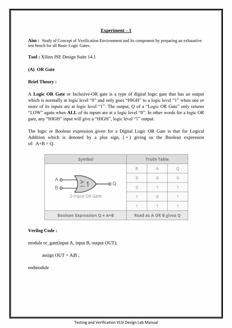
(A) OR Gate
Brief Theory :
A Logic OR Gate or Inclusive-OR gate is a type of digital logic gate that has an output
which is normally at logic level “0” and only goes “HIGH” to a logic level “1” when one or
more of its inputs are at logic level “1”. The output, Q of a “Logic OR Gate” only returns
“LOW” again when ALL of its inputs are at a logic level “0”. In other words for a logic OR
gate, any “HIGH” input will give a “HIGH”, logic level “1” output.
The logic or Boolean expression given for a Digital Logic OR Gate is that for Logical
Addition which is denoted by a plus sign, ( + ) giving us the Boolean expression
of: A+B = Q.
Verilog Code :
module or_gate(input A, input B, output OUT);
assign OUT = A|B ;
endmodule

Testing and Verification VLSI Design Lab Manual
RTL :
Verilog Test Bench :
module or_gate_test;
reg A;
reg B;
wire OUT;
or_gate uut (.A(A), .B(B), .OUT(OUT));
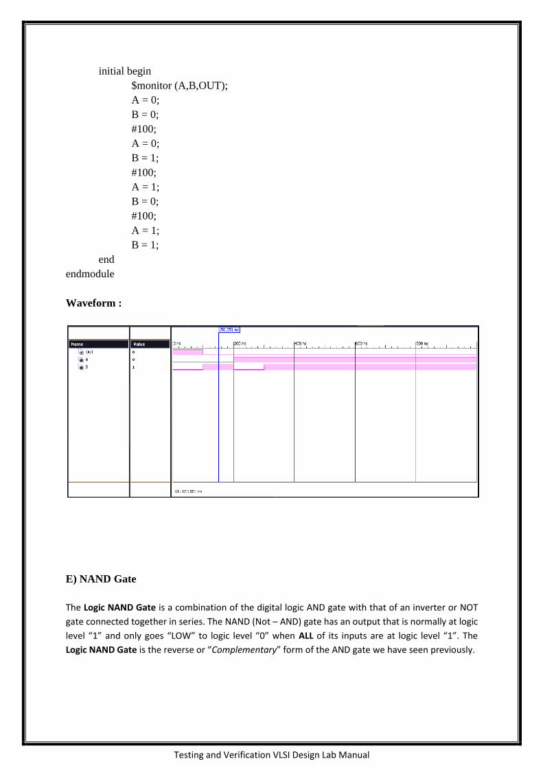
initial begin
$monitor(A,B,OUT);
A = 0;
B = 0;
#100;
A = 0;
B = 1;
#100;
A = 1;
B = 0;
#100;
A = 1;
B = 1;
end
endmodule
Waveform :

Testing and Verification VLSI Design Lab Manual
Conclusion :
(B) AND Gate
Brief Theory :
A Logic AND Gate is a type of digital logic gate that has an output which is normally at
logic level “0” and only goes “HIGH” to a logic level “1” when ALL of its inputs are at logic
level “1”. The output state of a “Logic AND Gate” only returns “LOW” again when ANY of
its inputs are at a logic level “0”. In other words for a logic AND gate, any LOW input will
give a LOW output.
The logic or Boolean expression given for a Digital Logic AND Gate is that for Logical
Multiplication which is denoted by a single dot or full stop symbol, ( . ) giving us the Boolean
expression of: A.B = Q.

Testing and Verification VLSI Design Lab Manual
Verilog Code :
module and_gate( input A, input B, output OUT);
assign OUT = A & B;
endmodule
RTL :
Verilog Test Bench :
module and_gate_test;
reg A;
reg B;
wire OUT;
and_gate uut (.A(A), .B(B), .OUT(OUT));
initial begin
$monitor(A,B,OUT);
A = 0;
B = 0;
#100;

Testing and Verification VLSI Design Lab Manual
A = 0;
B = 1;
#100;
A = 1;
B = 0;
#100;
A = 1;
B = 1;
end
endmodule
Waveform :
Conclusion :

Testing and Verification VLSI Design Lab Manual
C) NOT Gate
Brief Theory :
The digital Logic NOT Gate is the most basic of all the logical gates and is sometimes
referred to as an Inverting Buffer or simply a Digital Inverter. It is a single input device
which has an output level that is normally at logic level “1” and goes “LOW” to a logic level
“0” when its single input is at logic level “1”, in other words it “inverts” (complements) its
input signal. The output from a NOT gate only returns “HIGH” again when its input is at
logic level “0” giving us the Boolean expression of: A = Q.
Verilog Code :
module not_gate( input A, output OUT);
assign OUT = ~A;
endmodule
RTL :
Verilog Test Bench :

Testing and Verification VLSI Design Lab Manual
module not_gate_test;
reg A;
wire OUT;
not_gate uut (.A(A), .OUT(OUT));
initial begin
$monitor (A,OUT);
A = 0;
#100;
A = 1;
end
endmodule
Waveform :
Coclusion :
D) NOR Gate
The Logic NOR Gate or Inclusive-NOR gate is a combination of the digital logic OR gate
with that of an inverter or NOT gate connected together in series. The NOR (Not – OR) gate
has an output that is normally at logic level “1” and only goes “LOW” to logic level “0”

Testing and Verification VLSI Design Lab Manual
when ANY of its inputs are at logic level “1”. The Logic NOR Gate is the reverse or
“Complementary” form of the OR gate we have seen previously.
Verilog Code :
module nor_gate(input A, input B, output OUT);
assign OUT = ~(A | B);
endmodule
RTL :
Verilog Test Bench :
module nor_gate_test;
reg A;
reg B;
wire OUT;
nor_gate uut (.A(A), .B(B), .OUT(OUT));
Testing and Verification VLSI Design Lab Manual
initial begin
$monitor (A,B,OUT);
A = 0;
B = 0;
#100;
A = 0;
B = 1;
#100;
A = 1;
B = 0;
#100;
A = 1;
B = 1;
end
endmodule
Waveform :
E) NAND Gate
The Logic NAND Gate is a combination of the digital logic AND gate with that of an inverter or NOT
gate connected together in series. The NAND (Not – AND) gate has an output that is normally at logic
level “1” and only goes “LOW” to logic level “0” when ALL of its inputs are at logic level “1”. The
Logic NAND Gate is the reverse or “Complementary” form of the AND gate we have seen previously.

Testing and Verification VLSI Design Lab Manual
Verilog Code :
module nand_gate(input A, input B, output OUT);
assign OUT = ~(A & B);
endmodule
RTL :
Verilog Test Bench :
module nand_gate_test;
reg A;
reg B;
wire OUT;
nand_gate uut (.A(A), .B(B), .OUT(OUT));
initial begin
$monitor (A,B,OUT);
A = 0;
B = 0;
#100;

Testing and Verification VLSI Design Lab Manual
A = 0;
B = 1;
#100;
A = 1;
B = 0;
#100;
A = 1;
B = 1;
end
endmodule
Waveform :
Conclusion :

Testing and Verification VLSI Design Lab Manual
F) XOR Gate
Brief Theory :
There are two other types of digital logic gates which although they are not a basic gate in
their own right as they are constructed by combining together other logic gates, their output
Boolean function is important enough to be considered as complete logic gates. These two
“hybrid” logic gates are called the Exclusive-OR (Ex-OR) Gate and its complement the
Exclusive-NOR (Ex-NOR) Gate.
Output of an Exclusive-OR gate ONLY goes “HIGH” when its two input terminals are at
“DIFFERENT” logic levels with respect to each other.
Verilog Code :
module xor_gate(input A, input B, output OUT);
assign OUT = ((A & (~B)) | ((~A) & B));
endmodule
RTL :
Verilog Test Bench :
Testing and Verification VLSI Design Lab Manual
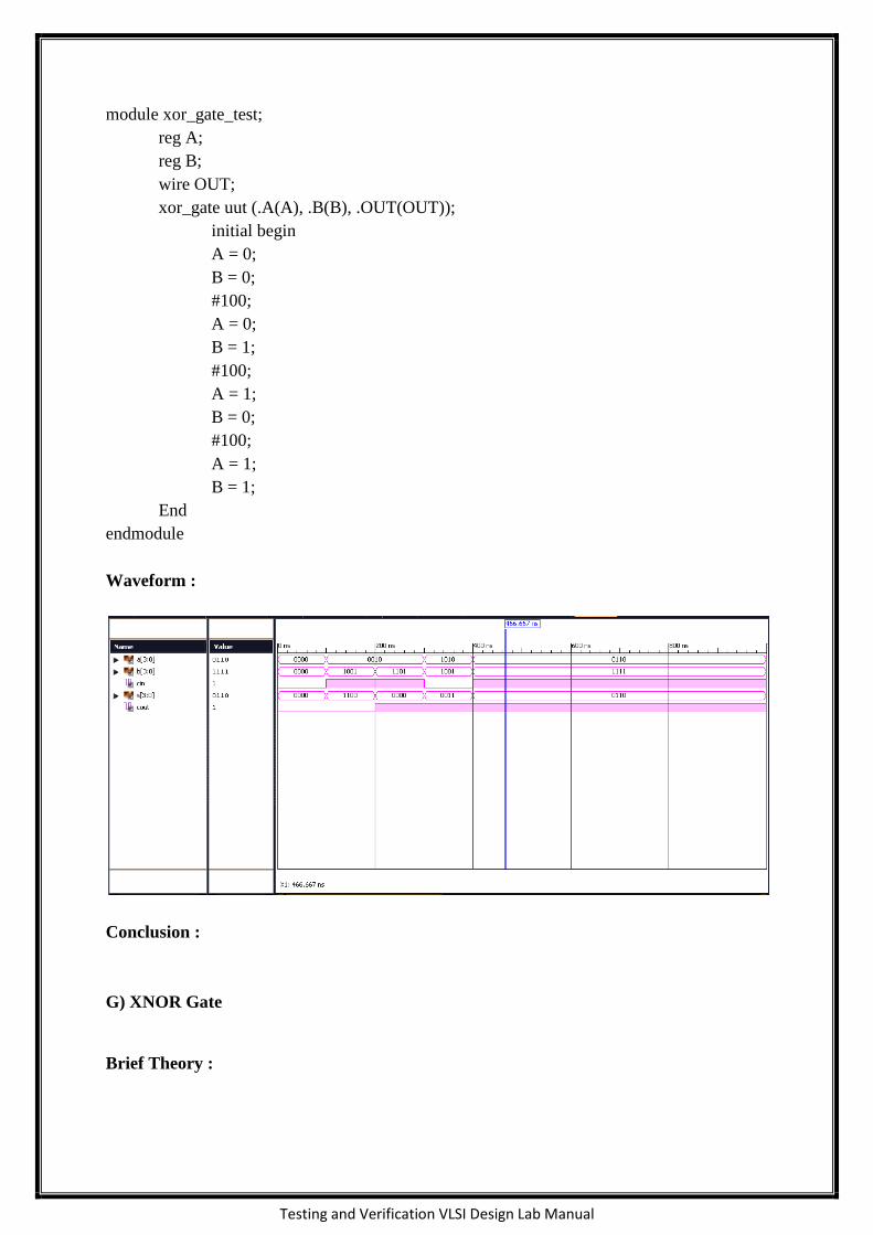
module xor_gate_test;
reg A;
reg B;
wire OUT;
xor_gate uut (.A(A), .B(B), .OUT(OUT));
initial begin
A = 0;
B = 0;
#100;
A = 0;
B = 1;
#100;
A = 1;
B = 0;
#100;
A = 1;
B = 1;
End
endmodule
Waveform :
Conclusion :
G) XNOR Gate
Brief Theory :

Testing and Verification VLSI Design Lab Manual
The Exclusive-NOR Gate function or Ex-NOR for short, is a digital logic gate that is the
reverse or complementary form of the Exclusive-OR function we look at in the previous
tutorial. Basically the “Exclusive-NOR Gate” is a combination of the Exclusive-OR gate and
the NOT gate but has a truth table similar to the standard NOR gate in that it has an output
that is normally at logic level “1” and goes “LOW” to logic level “0” when ANY of its inputs
are at logic level “1”.
However, an output “1” is only obtained if BOTH of its inputs are at the same logic level,
either binary “1” or “0”. For example, “00” or “11”. This input combination would then give
us the Boolean expression of: Q = (A B) = A.B + A.B
Verilog Code :
module xnor_gate(input A, input B, output OUT);
assign OUT = ((A & B) | ((~A) & (~B)));
endmodule
RTL :

Testing and Verification VLSI Design Lab Manual
Verilog Test Bench :
module xnor_gate_test;
reg A;
reg B;
wire OUT;
xnor_gate uut (.A(A), .B(B), .OUT(OUT));
initial begin
A = 0;
B = 0;
#100;
A = 0;
B = 1;
#100;
A = 1;
B = 0;
#100;
A = 1;
B = 1;
end
endmodule
Waveform :

Testing and Verification VLSI Design Lab Manual
Conclusion :