vertical power electronic devices based on bulk gan...
TRANSCRIPT
Vertical Power Electronic Devices Based on Bulk GaN Substrates
Dr. Isik C. Kizilyalli, CTO and Founder
Avogy, Inc.
677 River Oaks Parkway, San Jose, CA 95134
Partially funded by ARPA-E SWITCHES (Dr. T. Heidel)ONR-N00014-14-C-0087 (Dr. P. Maki)
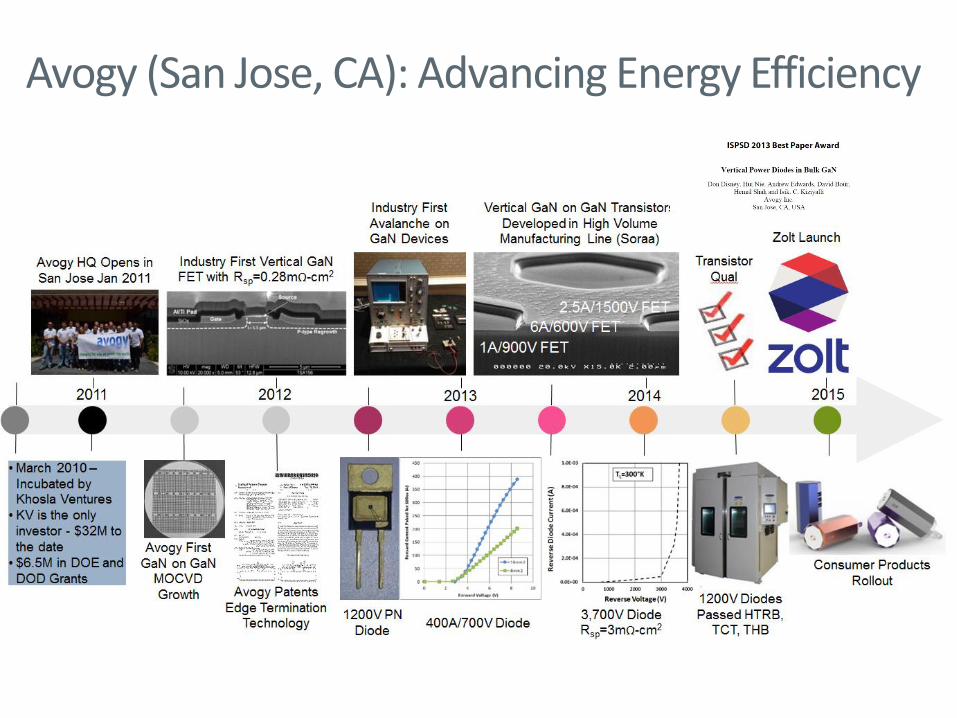
Avogy (San Jose, CA): Advancing Energy Efficiency

Vision and Mission for Vertical GaN Devices
Power Supplies*
Solar EV WindMotorDrive
UPS/Grid/Rail/Ship
Voltage (V) 600-1200 600 - 1200 600 - 1200 1200 - 3300 600 - 1200 1200 - 3300
Current (A) 0.5 – 20A 1 – 75A 50 – 200A 100 – 200A 2 – 100A 100 – 400A
Devices in Systems
Today
Si MOSFETSi PN
SiC SBD
Si MOSFETSi IGBTSi PN
SiC SBD
Si IGBTSi PN
Si IGBTSi PN
Si IGBTSi PN
Si IGBTSi Thyristor
Si PIN
Vision:Every power system in the world will utilize a vertical GaN device, circuit, technology, or science developed by 2030
Mission:The most efficient and compact power systems in the world are enabled by vertical GaN technologies
*Smart homes, LED drivers, laptops, mobile devices, data centers
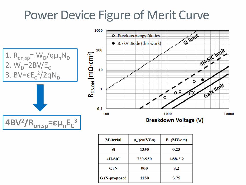
Power Device Figure of Merit Curve
4
4BV2/Ron,sp=εμnEC3
1. Ron,sp= WD/qμnND
2. WD=2BV/EC
3. BV=εEC2/2qND

GaN-on-GaN means less chip areaFor a given on-resistance (Ron) of 10mΩ:
500mΩ, 50 chips 40mΩ, 4 chips 10mΩ, 1 chip
GaN-on-GaNSiC
GaN-on-SiSi-MOSFET
GaN-on-GaN lowers die costwhile improving Ron ×Coff
switching characteristic
5

Schematic of a Boost Converter
Switch frequency increases → Optimum L and C Decreases
Vi is boosted to Vo
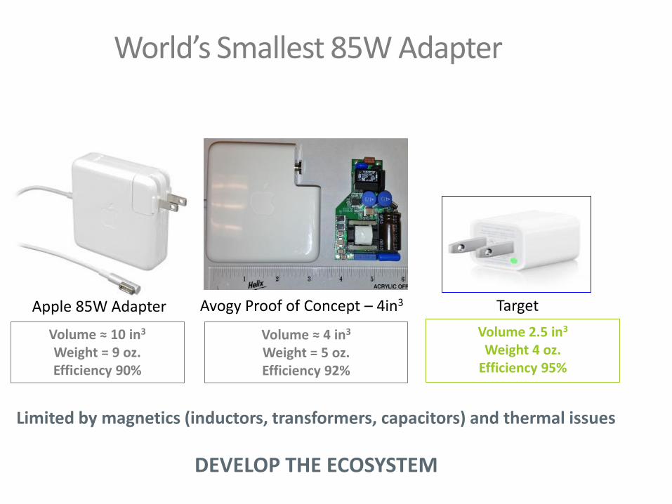
Volume ≈ 4 in3
Weight = 5 oz.Efficiency 92%
World’s Smallest 85W Adapter
Volume ≈ 10 in3
Weight = 9 oz.Efficiency 90%
Volume 2.5 in3
Weight 4 oz.Efficiency 95%
Avogy Proof of Concept – 4in3Apple 85W Adapter Target
Limited by magnetics (inductors, transformers, capacitors) and thermal issues
DEVELOP THE ECOSYSTEM
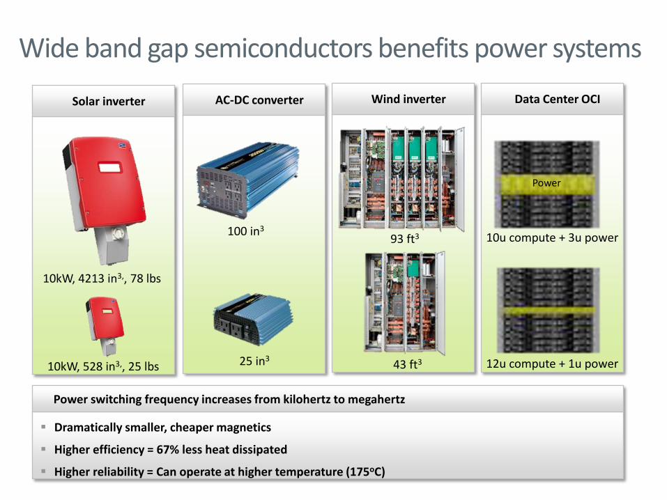
Data Center OCIWind inverterAC-DC converterSolar inverter
Wide band gap semiconductors benefits power systems
Dramatically smaller, cheaper magnetics
Higher efficiency = 67% less heat dissipated
Higher reliability = Can operate at higher temperature (175oC)
Power switching frequency increases from kilohertz to megahertz
10u compute + 3u power
12u compute + 1u power
Power
93 ft3
43 ft3
10kW, 4213 in3,, 78 lbs
10kW, 528 in3,, 25 lbs
100 in3
25 in3

WOCSEMMAD 2015
Bulk GaN vs. GaN-on-Si/SiCAttributes GaN on Si GaN on SiC GaN on Bulk-GaN
Defect Density (cm-2) 109 5x10⁸ 103 to 106
Lattice Mismatch, % 17 3.5 0
CTE Mismatch, % 54 25 0
Layer Thickness (µm) < 5 < 10 > 50
Breakdown Voltage (V) < 1000 < 2000 > 5000
Avalanche Capability No No Yes
Device Types Lateral Lateral Vertical and Lateral
Microscopy and Growth

Vertical FET Advantages over Lateral HEMTs
• Grow thick GaN layers: Drift region BV >> 1200V• Reduced number of defects: Improved Reliability, Large EC
• Breakdown occurs in bulk and not surface, avalanche capability• Current flow vertical and not parallel to surface• Realize high current (>> 20A) devices, Normally-off operation• For the same Rdson , a VFET is smaller than a HEMT
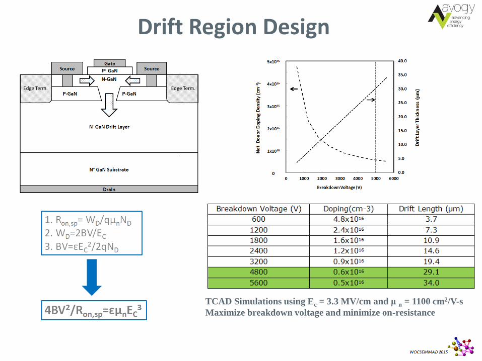
Drift Region Design
TCAD Simulations using Ec = 3.3 MV/cm and μ n = 1100 cm2/V-s
Maximize breakdown voltage and minimize on-resistance
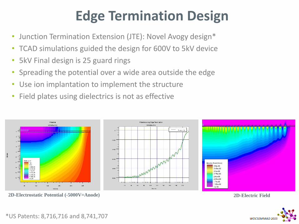
Edge Termination Design• Junction Termination Extension (JTE): Novel Avogy design*
• TCAD simulations guided the design for 600V to 5kV device
• 5kV Final design is 25 guard rings
• Spreading the potential over a wide area outside the edge
• Use ion implantation to implement the structure
• Field plates using dielectrics is not as effective
2D-Electrostatic Potential (-5000V=Anode) 2D-Electric Field
*US Patents: 8,716,716 and 8,741,707
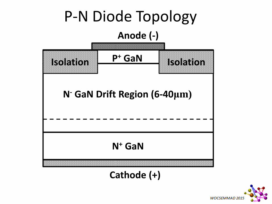
N+ GaN
N- GaN Drift Region (6-40μm)
P+ GaNIsolation Isolation
Cathode (+)
Anode (-)
P-N Diode Topology
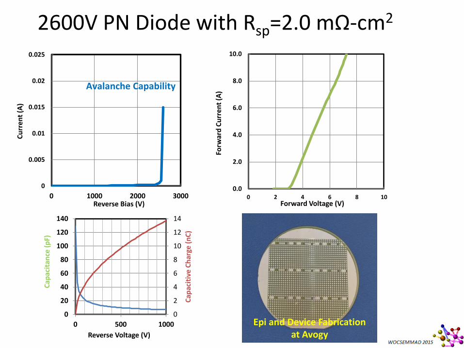
2600V PN Diode with Rsp=2.0 mΩ-cm2
0
0.005
0.01
0.015
0.02
0.025
0 1000 2000 3000
Cu
rren
t (A
)
Reverse Bias (V)
Avalanche Capability
0.0
2.0
4.0
6.0
8.0
10.0
0 2 4 6 8 10
Forw
ard
Cu
rren
t (A
)
Forward Voltage (V)
Epi and Device Fabrication at Avogy
0
2
4
6
8
10
12
14
0
20
40
60
80
100
120
140
0 500 1000
Cap
acit
ive
Ch
arge
(n
C)
Cap
acit
ance
(p
F)
Reverse Voltage (V)

Avalanche capability
• GaN devices do have avalanche capability
• PN diodes with 1700V epi design in TO-220 packages
• Current pulse width of 30ms, up to 15mA
• Avalanche energy in each pulse > 900mJ
0
2
4
6
8
10
12
14
16
0 500 1000 1500 2000 2500
IR (
mA
)
VR (V)
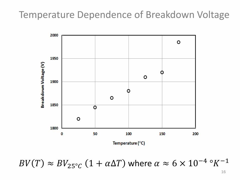
Temperature Dependence of Breakdown Voltage
16
𝐵𝑉 𝑇 ≈ 𝐵𝑉25°𝐶 1 + 𝛼∆𝑇 where 𝛼 ≈ 6 × 10⁻⁴ °𝐾−1
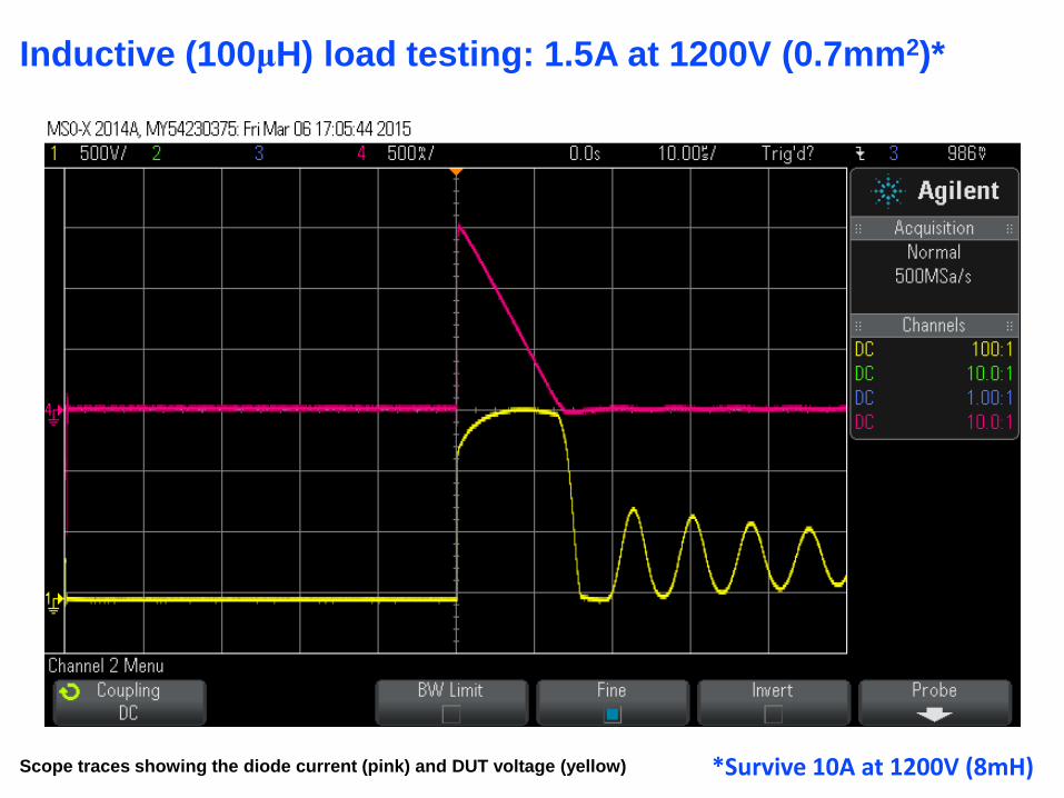
Inductive (100μH) load testing: 1.5A at 1200V (0.7mm2)*
Scope traces showing the diode current (pink) and DUT voltage (yellow) *Survive 10A at 1200V (8mH)
DUT
Schottkydiode
InductorCPower Supply
PulseGenerator
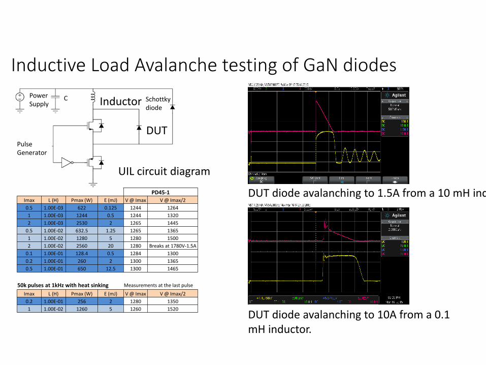
DUT diode avalanching to 1.5A from a 10 mH inductor
DUT diode avalanching to 10A from a 0.1 mH inductor.
UIL circuit diagram
Inductive Load Avalanche testing of GaN diodes
PD45-1
Imax L (H) Pmax (W) E (mJ) V @ Imax V @ Imax/2
0.5 1.00E-03 622 0.125 1244 1264
1 1.00E-03 1244 0.5 1244 1320
2 1.00E-03 2530 2 1265 1445
0.5 1.00E-02 632.5 1.25 1265 1365
1 1.00E-02 1280 5 1280 1500
2 1.00E-02 2560 20 1280 Breaks at 1780V-1.5A
0.1 1.00E-01 128.4 0.5 1284 1300
0.2 1.00E-01 260 2 1300 1365
0.5 1.00E-01 650 12.5 1300 1465
50k pulses at 1kHz with heat sinking Measurements at the last pulse
Imax L (H) Pmax (W) E (mJ) V @ Imax V @ Imax/2
0.2 1.00E-01 256 2 1280 1350
1 1.00E-02 1260 5 1260 1520
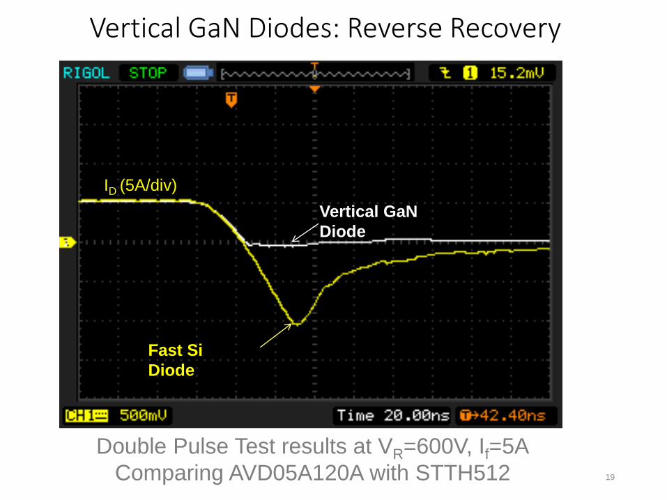
Vertical GaN Diodes: Reverse Recovery
19
ID (5A/div)
Fast Si
Diode
Vertical GaN
Diode
Double Pulse Test results at VR=600V, If=5A
Comparing AVD05A120A with STTH512
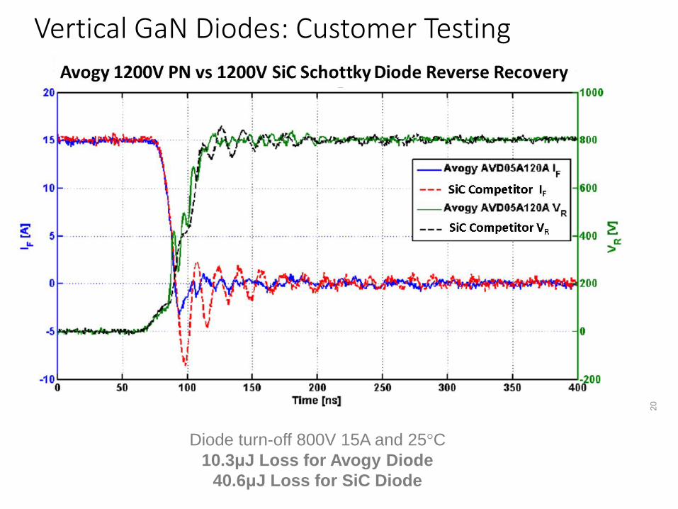
Vertical GaN Diodes: Customer Testing
Diode turn-off 800V 15A and 25°C
10.3μJ Loss for Avogy Diode
40.6μJ Loss for SiC Diode
20
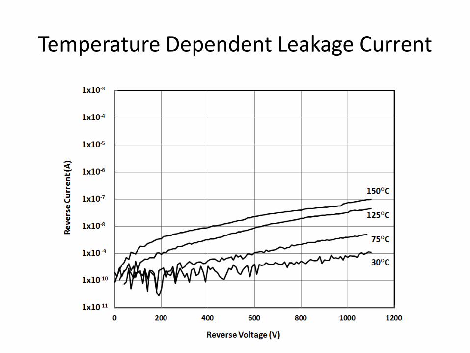
Temperature Dependent Leakage Current

3.7kV Diode with Rsp=2.95mW-cm2
• ND ≈ 5x1015 cm-3 (measured by C-V)• Drift layer thickness is 40μm• Edge termination designed for 5kV• Next ND ≈ 2-3x1015 cm-3 and 50μm

Measured Forward I-V PN-Diode Drift Region= 40μm
mn =1760(TL/300)-3/2 cm2/V-sElectron mobility in low-defect GaN > 1700 cm2/V-s
Diode Area ≈ 0.12 mm2

Minority Carrier Lifetime (τp ≈ 2ns)

I=400A for BV=700V PN Diodes
Agilent high power network analyzer
(Pulsed at 100μs)
J=2.5kA/cm2Demo 100A DC and BV=1400V
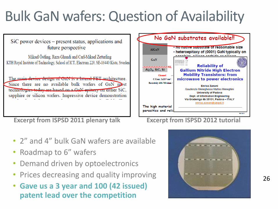
Bulk GaN wafers: Question of Availability
• 2” and 4” bulk GaN wafers are available
• Roadmap to 6” wafers
• Demand driven by optoelectronics
• Prices decreasing and quality improving
• Gave us a 3 year and 100 (42 issued) patent lead over the competition
Excerpt from ISPSD 2012 tutorialExcerpt from ISPSD 2011 plenary talk
26
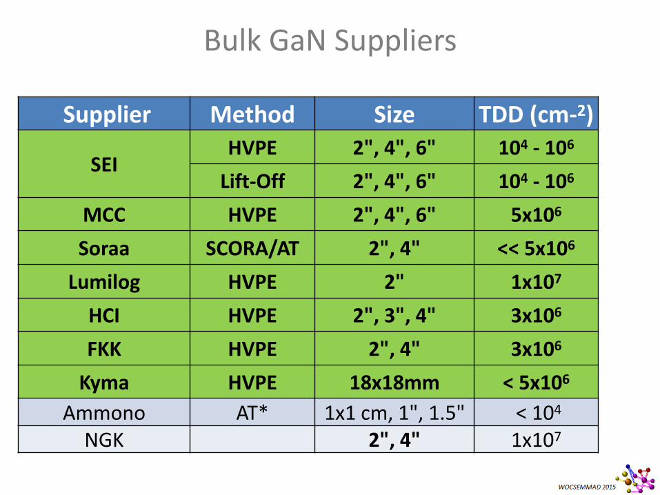
Bulk GaN Suppliers
Supplier Method Size TDD (cm-2)
SEIHVPE 2", 4", 6" 104 - 106
Lift-Off 2", 4", 6" 104 - 106
MCC HVPE 2", 4", 6" 5x10⁶
Soraa SCORA/AT 2", 4" << 5x10⁶
Lumilog HVPE 2" 1x10⁷
HCI HVPE 2", 3", 4" 3x10⁶
FKK HVPE 2", 4" 3x10⁶
Kyma HVPE 18x18mm < 5x10⁶
Ammono AT* 1x1 cm, 1", 1.5" < 104
NGK 2", 4" 1x10⁷
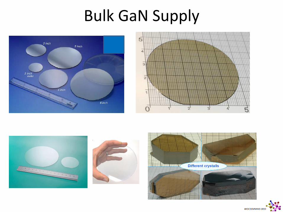
Bulk GaN Supply

1200-1700V PN Diode Trend Charts
# of diodes ≈ 40000

Avogy Inc. | Confidential under NDA | 4/19/2015 30
Test Lot Qty 168hr 500hr 1000hr Notes
HTRB(150˚C, 960V)
PD59 77 0/77 0/77 0/77 HTRB device qualification completeFailure mechanism identified and solved Substrate specification patented
PD66 77 0/77 0/77 0/77
PD67 77 0/77 0/77 0/77
THB(85˚C, 85%RH, 80V)
PD59 77 0/77 0/77 0/77 THB device qualification complete
PD60 77 0/77 0/77 0/77
PD66 77 0/77 0/77 0/77
PD77 77 0/77 0/77 0/77
HTOL
PD67/68 77 0/77 0/77 0/77 Working with substrate vendors/specs1. Pass HTOL with Substrate Vendor A,B2. Fail HTOL with Substrate Vendor C, D• No change in BV, Imax, or Ron• Shift in leakage current
PD77 77
PD77 77
PD77 77
TCT(-65˚C to 150˚C,
100/500/1000cyc)
PD68 77 0/77 0/77 0/77 TCT device qualification completePD77 77 0/77 0/77 0/77
PD77 77 0/77 0/77 0/77
PD78 77 0/77 0/77 0/77
PD76 77 0/77 0/77 0/77
1200V PN Diode Qualification/Reliability
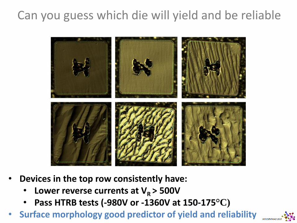
Can you guess which die will yield and be reliable
• Devices in the top row consistently have:• Lower reverse currents at VR > 500V • Pass HTRB tests (-980V or -1360V at 150-175°C)
• Surface morphology good predictor of yield and reliability

Comparison between prediction with test data
Correlation valid for all substrate vendors, MOCVD tools
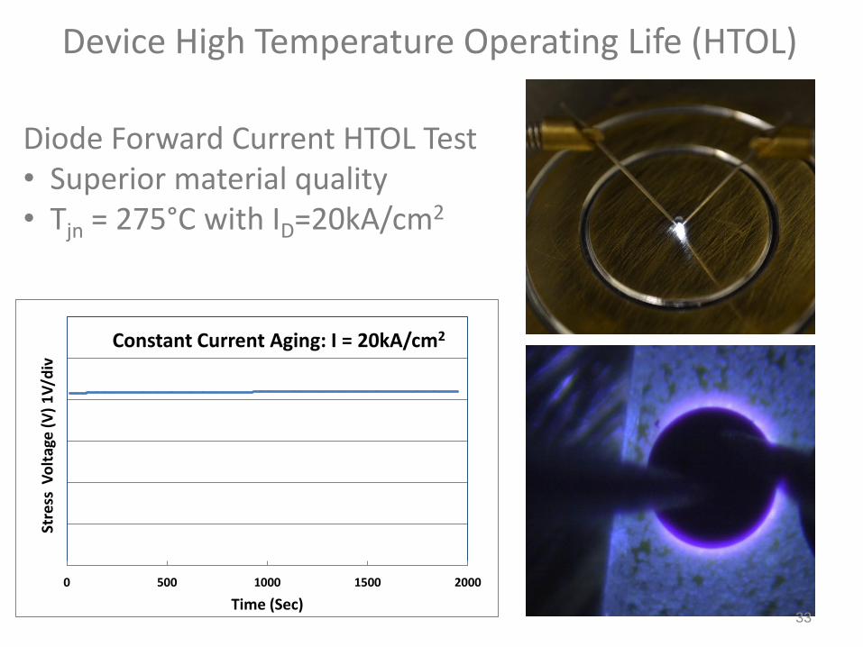
Device High Temperature Operating Life (HTOL)
Diode Forward Current HTOL Test• Superior material quality• Tjn = 275°C with ID=20kA/cm2
0 500 1000 1500 2000
Stre
ss V
olt
age
(V
) 1
V/d
iv
Time (Sec)
Constant Current Aging: I = 20kA/cm2
33

GaN p-n diodes on SCORA wafers
No JTE Device BV = 500-680VSub-threshold ideality n=25 substrates 13x13 mm2
Device Area = 0.11mm2
SCORA Substrates as Received
Diodes at Test

Parameter Extraction: Measurement versus Simulation
Forward current: Best fit obtained with τp = 1 ns and μn = 900-1000 cm2/V-s
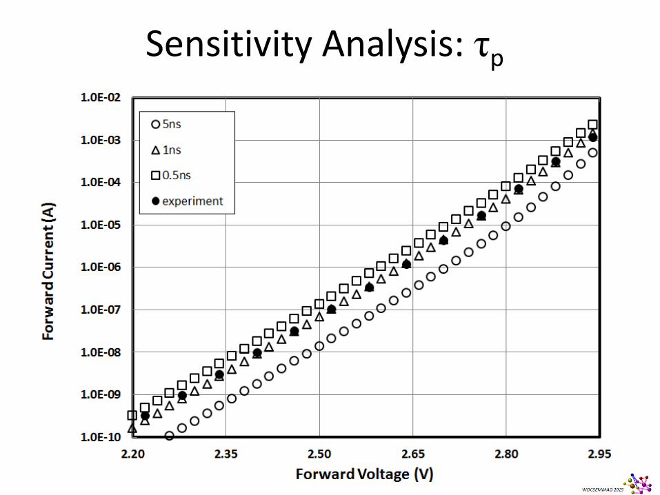
Sensitivity Analysis: τp

WOCSEMMAD 2015
Substrates from Na-flux method

WOCSEMMAD 2015
Vertical GaN FET Devices: Keep the Structures Simple
Bardeen-Brattain Transistor, Bell Labs 1947

2D Simulation of Current Flow
39

Vertical FET Structure
40

FET Layout and Process
Source
Gate
Pad
Buried p-layerGate
channel channel
FET Total Area
0.17mm2
FET Active Area
0.13mm2
41

Multiple MOCVD Growths for Transistor
42

1.5kV 2.2mΩ-cm2 ‘Normally-Off’ Vertical GaN FET
43

Performance Gap Between FET and P-N Diode
44Need to Improve the BV and RDS,ON for the FET

Vertical FET Structure II
45

46
Introducing the Zolt Laptop Charger Plus
World’s Smallest, Lightest and Smartest Laptop Power Charger.
© Copyright 2015 Avogy Inc. | Introduction for Investors | Proprietary & Confidential
4x Smaller | 3x Lighter | Laptops | Tablets | Phones | and more..

47
Smart 3-in-1 Charging
Power your laptop
and two mobile
devices -
simultaneously.
Zolt also powers your
GoPro, portable
speakers, camera
and more.
© Copyright 2015 Avogy Inc. | Introduction for Investors | Proprietary & Confidential
Compatible w/ 90%+ of
Laptops