vhdl & fpga. (4) -...
TRANSCRIPT

310/1780-12
ICTP-INFN Advanced Tranining Course onFPGA and VHDL for Hardware Simulation and Synthesis
27 November - 22 December 2006
���������������������������������������������������������������������
���� � ���� � ������� �
Nizar ABDALLHACTEL Corp.
2061 Stierlin CourtMountain View, CA 94043-4655
U.S.A.
________________________________________________________________These lecture notes are intended only for distribution to participants

VHDL & FPGA ArchitecturesNizar Abdallah, [email protected]

© 2006 Nizar Abdallah / Actel Corp. 2VHDL & FPGA Architectures November, 2006
OutlineIntroduction to FPGA & FPGA Design Flow
Synthesis I – Introduction
Synthesis II - Introduction to VHDL
Synthesis III - Advanced VHDL
Design verification & timing concepts
Programmable logic & FPGA architectures
Actel ProASIC3 FPGA architecture

Design Verification andTiming Concepts

© 2006 Nizar Abdallah / Actel Corp. 4VHDL & FPGA Architectures November, 2006
Timing in the Design Flow
Timing Driven Synthesis
Timing Driven Optimization
Timing Driven Floor-Planner
Timing Driven Place & Route

© 2006 Nizar Abdallah / Actel Corp. 5VHDL & FPGA Architectures November, 2006
Simulators versus Verifiers
SimulatorsCircuit-LevelTimingSwitch-LevelLogic-Level
Verifiers (Pattern Independent)Static Timing Analysis
© 2006 Nizar Abdallah / Actel Corp. 6VHDL & FPGA Architectures November, 2006
Timing Driven Methodology
Golden Rule:
Detect Problems as early as possibleDetect Problems as early as possible

© 2006 Nizar Abdallah / Actel Corp. 7VHDL & FPGA Architectures November, 2006
What are Timing Constraints?
Maximum or minimum limits placed on timing paths
Usually expressed in ns. or ps.
There are basically 4 types of timing paths in a synthesized digital design:
Input to registersRegisters to outputInput to outputRegisters to registers
To understand timing paths we first must understand flip-flop timing parameters

© 2006 Nizar Abdallah / Actel Corp. 8VHDL & FPGA Architectures November, 2006
Timing Paths
These basic timing paths can apply to:A module within an ASIC/FPGAA whole ASIC/FPGAA system with multiple chips
© 2006 Nizar Abdallah / Actel Corp. 9VHDL & FPGA Architectures November, 2006
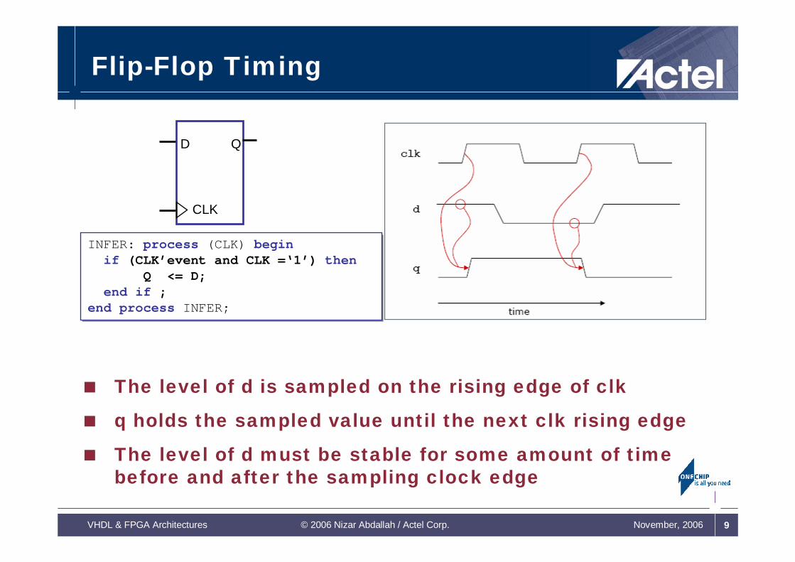
Flip-Flop Timing
The level of d is sampled on the rising edge of clk
q holds the sampled value until the next clk rising edge
The level of d must be stable for some amount of time before and after the sampling clock edge
CLK
D Q
INFER: process (CLK) beginif (CLK’event and CLK =‘1’) then
Q <= D;end if ;
end process INFER;
INFER: process (CLK) beginif (CLK’event and CLK =‘1’) then
Q <= D;end if ;
end process INFER;
© 2006 Nizar Abdallah / Actel Corp. 10VHDL & FPGA Architectures November, 2006
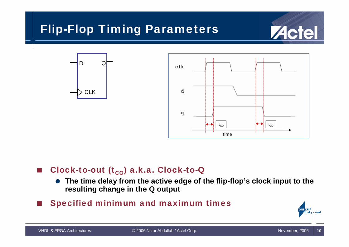
Flip-Flop Timing Parameters
Clock-to-out (tCO) a.k.a. Clock-to-QThe time delay from the active edge of the flip-flop’s clock input to the resulting change in the Q output
Specified minimum and maximum times
CLK
D Q

© 2006 Nizar Abdallah / Actel Corp. 11VHDL & FPGA Architectures November, 2006
Flip-Flop Timing Parameters (cont’d)
Input Setup (tS)The minimum time that the D input must be stable before the active (rising or falling) edge of the clock
CLK
D Q

© 2006 Nizar Abdallah / Actel Corp. 12VHDL & FPGA Architectures November, 2006
Flip-Flop Timing Parameters (cont’d)
Input Hold (tH)The minimum time that the D input must be stable after the active edge of the clock
CLK
D Q
© 2006 Nizar Abdallah / Actel Corp. 13VHDL & FPGA Architectures November, 2006
Flip-Flop Timing Parameters (cont’d)
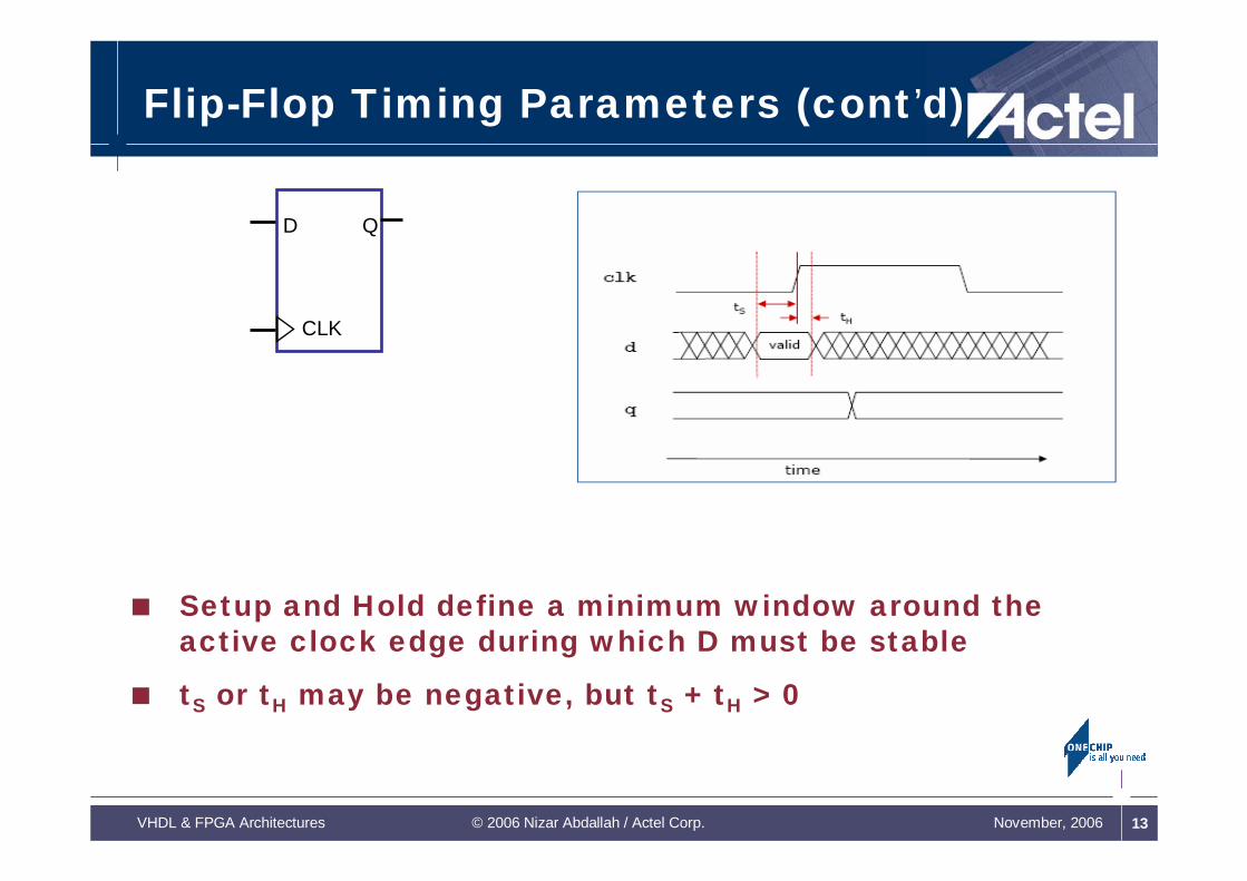
Setup and Hold define a minimum window around the active clock edge during which D must be stable
tS or tH may be negative, but tS + tH > 0
CLK
D Q

© 2006 Nizar Abdallah / Actel Corp. 14VHDL & FPGA Architectures November, 2006
Flip-Flop Timing Parameters (cont’d)
Clock ParametersClock cycle time (tCYC), minimumClock pulse width high (tCH), minimumClock pulse width low (tCL), minimum
CLK
D Q

© 2006 Nizar Abdallah / Actel Corp. 15VHDL & FPGA Architectures November, 2006
Constraining FPGA Designs with SDC
Source: Mentor Graphics Corporation ©, 2002
create_clock
set_multicycle_path
set_false_path
set_output_delay
set_input_delay
Constraining Designs @ Board-Level

© 2006 Nizar Abdallah / Actel Corp. 16VHDL & FPGA Architectures November, 2006
Constraining Designs
Design EnvironmentOperating conditions (Process / Voltage / Temperature)
Worst: to fix the setup violationsTypical: mostly ignoredBest: to fix the hold violations
Timing Assertions (Design-level)Clock CharacteristicsArrival Time at Each Input PortRequired Time at Each Output Port
Timing ExceptionsFalse PathsMaximum Path DelayMinimum Path DelayMulti-cycle Paths
© 2006 Nizar Abdallah / Actel Corp. 17VHDL & FPGA Architectures November, 2006
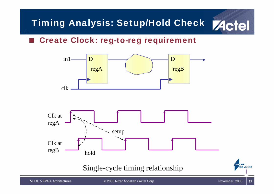
Timing Analysis: Setup/Hold Check
Create Clock: reg-to-reg requirement
regA regB
D Din1
clk
Clk atregA
Clk atregB
setup
hold
Single-cycle timing relationship

© 2006 Nizar Abdallah / Actel Corp. 18VHDL & FPGA Architectures November, 2006
Setup Check
Arrival/Required
Ck0
Slack = Required_time – Arrival_time (Violation if < 0)
20
FF2:D Arrival Time
FF2FF2FF1FF1
CK
D
CPCP
FF2:D Required Time
slack
40
FF2:CP
FF1:CP – FF2:D
20
CK-FF2:CP
15
= 30= 33
= +3
-STP
2
35FF1:CP
10
CK–FF1:CP
10
© 2006 Nizar Abdallah / Actel Corp. 19VHDL & FPGA Architectures November, 2006
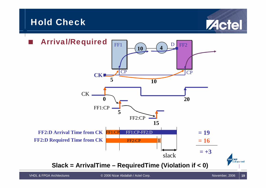
Hold Check
Arrival/Required
CK0
Slack = ArrivalTime – RequiredTime (Violation if < 0)
20
FF2:D Arrival Time from CKFF2:D Required Time from CK
slack
FF2:CP
= 19= 16
= +3
15
FF1:CP5
FF2FF2FF1FF1
CK
D
CPCP
10
FF1:CP-FF2:D
105
FF1:CP
FF2:CP 1
4

© 2006 Nizar Abdallah / Actel Corp. 20VHDL & FPGA Architectures November, 2006
Timing Analysis: Multi-cycle
set_multicycle_path: reg-to-reg exception
regA regB
D Din1
clk
Clk atregA
Clk atregB
setup
multi-cycle timing relationship

© 2006 Nizar Abdallah / Actel Corp. 21VHDL & FPGA Architectures November, 2006
2.0ns
Input Delay Constraints
Captures External Setup/Hold RequirementsMyDesign
ClockGenerator
CK
CK
IN
SDC: set_input_delay 2.0 -clock CK {IN}
3.0ns
Option “-min” for hold checkOption “-max” for setup check

© 2006 Nizar Abdallah / Actel Corp. 22VHDL & FPGA Architectures November, 2006
Constraining Designs
Set Input Delay: setup/hold requirements
Valid Data
0 15 30
23 ns 7 ns
clk
datain
> set_input_delay -max 23.0 -min 0.0 -clock clk {datain}
© 2006 Nizar Abdallah / Actel Corp. 23VHDL & FPGA Architectures November, 2006
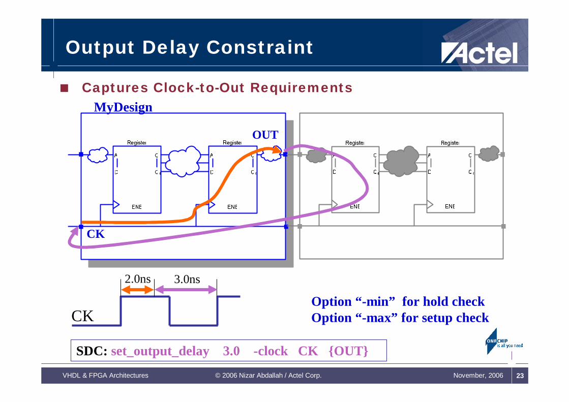
Output Delay Constraint
Captures Clock-to-Out Requirements
2.0ns
MyDesign
CK
CK
OUT
SDC: set_output_delay 3.0 -clock CK {OUT}
3.0ns
Option “-min” for hold checkOption “-max” for setup check
© 2006 Nizar Abdallah / Actel Corp. 24VHDL & FPGA Architectures November, 2006
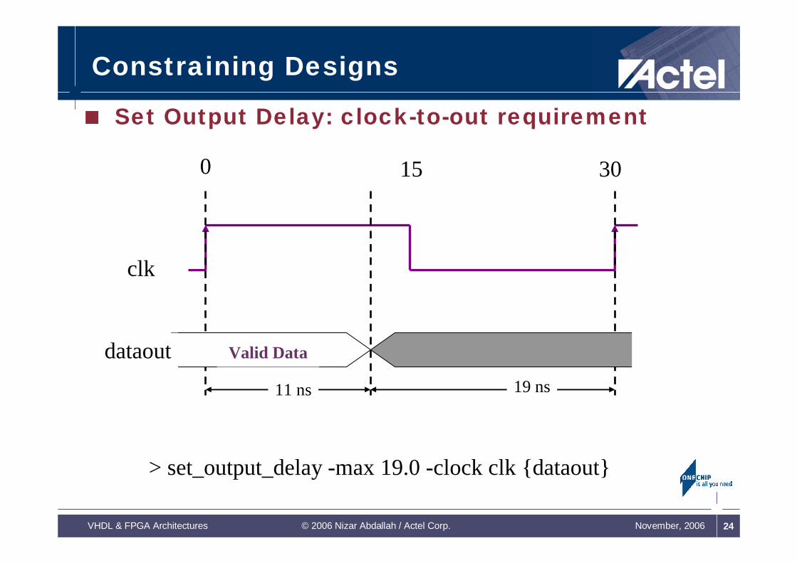
Constraining Designs
Set Output Delay: clock-to-out requirement
Valid Data
0 15 30
11 ns 19 ns
clk
dataout
> set_output_delay -max 19.0 -clock clk {dataout}

© 2006 Nizar Abdallah / Actel Corp. 25VHDL & FPGA Architectures November, 2006
Cross-Domain Analysis
Study over the Least Common Multiplier
common period

© 2006 Nizar Abdallah / Actel Corp. 26VHDL & FPGA Architectures November, 2006
Design OverviewBlock Diagram
PCI FPGA
FPGA 1
FPGA 2
FPGA 3
PCI BUS
Local Bus
1553 BC
128K x 8SRAM
128K x 8SRAM
Shared SRAM
© 2006 Nizar Abdallah / Actel Corp. 27VHDL & FPGA Architectures November, 2006
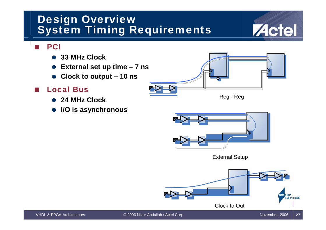
Design OverviewSystem Timing Requirements
PCI33 MHz ClockExternal set up time – 7 nsClock to output – 10 ns
Local Bus24 MHz ClockI/O is asynchronous
Reg - Reg
External Setup
Clock to Out
© 2006 Nizar Abdallah / Actel Corp. 28VHDL & FPGA Architectures November, 2006
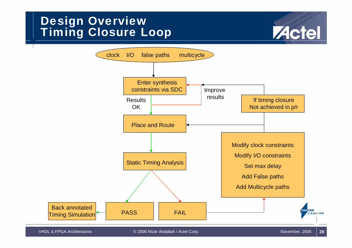
Design OverviewTiming Closure Loop
Enter synthesisconstraints via SDC
Place and Route
Improve resultsResults
OK
Static Timing Analysis
PASS FAIL
clock I/O false paths multicycle
Modify clock constraints
Modify I/O constraints
Set max delay
Add False paths
Add Multicycle paths
If timing closureNot achieved in p/r
Back annotatedTiming Simulation