video input processor (vip) - product.ic114.comproduct.ic114.com/pdf/s/saa7111_3.pdf · 8.2.1...
TRANSCRIPT

DATA SHEET
Product specificationSupersedes data of 1996 Oct 30File under Integrated Circuits, IC22
1998 May 15
INTEGRATED CIRCUITS
SAA7111Video Input Processor (VIP)

1998 May 15 2
Philips Semiconductors Product specification
Video Input Processor (VIP) SAA7111
CONTENTS
1 FEATURES
2 APPLICATIONS
3 GENERAL DESCRIPTION
4 QUICK REFERENCE DATA
5 ORDERING INFORMATION
6 BLOCK DIAGRAM
7 PINNING
8 FUNCTIONAL DESCRIPTION
8.1 Analog input processing8.2 Analog control circuits8.2.1 Clamping8.2.2 Gain control8.3 Chrominance processing8.4 Luminance processing8.5 RGB matrix8.6 VPO-bus (digital outputs)8.7 Synchronization8.8 Clock generation circuit8.9 Power-on reset and CE input8.10 RTCO output8.11 The Line-21 text slicer8.11.1 Suggestions for I2C-bus interface of the display
software reading line-21 data
9 GAIN CHARTS
10 LIMITING VALUES
11 CHARACTERISTICS
12 TIMING DIAGRAMS
13 CLOCK SYSTEM
13.1 Clock generation circuit13.2 Power-on control
14 OUTPUT FORMATS
15 APPLICATION INFORMATION
15.1 Layout hints
16 I2C-BUS DESCRIPTION
16.1 I2C-bus format16.2 I2C-bus detail16.2.1 Subaddress 0016.2.2 Subaddress 0216.2.3 Subaddress 0316.2.4 Subaddress 0416.2.5 Subaddress 0516.2.6 Subaddress 0616.2.7 Subaddress 0716.2.8 Subaddress 0816.2.9 Subaddress 09
16.2.10 Subaddress 0A16.2.11 Subaddress 0B16.2.12 Subaddress 0C16.2.13 Subaddress 0D16.2.14 Subaddress 0E16.2.15 Subaddress 1016.2.16 Subaddress 1116.2.17 Subaddress 1216.2.18 Subaddress 1A (read-only register)16.2.19 Subaddress 1B (read-only register)16.2.20 Subaddress 1C (read-only register)16.2.21 Subaddress 1F (read-only register)
17 FILTER CURVES
17.1 Anti-alias filter curve17.2 Luminance filter curves17.3 Chrominance filter curves
18 I2C START SET-UP
19 PACKAGE OUTLINE
20 SOLDERING
20.1 Introduction20.2 Reflow soldering20.3 Wave soldering20.3.1 PLCC20.3.2 QFP20.3.3 Method (PLCC and QFP)20.4 Repairing soldered joints
21 DEFINITIONS
22 LIFE SUPPORT APPLICATIONS
23 PURCHASE OF PHILIPS I2C COMPONENTS

1998 May 15 3
Philips Semiconductors Product specification
Video Input Processor (VIP) SAA7111
1 FEATURES
• Four analog inputs, internal analog source selectors,e.g. 4 × CVBS or 2 × Y/C or (1 × Y/C and 2 × CVBS)
• Two analog preprocessing channels
• Fully programmable static gain for the main channels orautomatic gain control for the selected CVBS or Y/Cchannel
• Switchable white peak control
• Two built-in analog anti-aliasing filters
• Two 8-bit video CMOS analog-to-digital converters(ADCs)
• On-chip clock generator
• Line-locked system clock frequencies
• Digital PLL for H-sync processing and clock generation
• Requires only one crystal (24.576 MHz) for all standards
• Horizontal and vertical sync detection
• Automatic detection of 50/60 Hz field frequency andautomatic switching between standards PAL and NTSC
• Luminance and chrominance signal processing forPAL BGHI, PAL N, PAL M, NTSC M, NTSC N andNTSC 4.43
• User programmable luminance peaking or aperturecorrection
• Cross-colour reduction for NTSC by chrominance combfiltering
• PAL delay line for correcting PAL phase errors
• Real time status information output (RTCO)
• Brightness Contrast Saturation (BCS) control on-chip
• The YUV (CCIR-601) bus supports a data rate of:
– 864 × fH = 13.5 MHz for 625 line sources
– 858 × fH = 13.5 MHz for 525 line sources.
• Data output streams for 16, 12 or 8-bit width with thefollowing formats:
– 411 YUV (12-bit)
– 422 YUV (16-bit)
– 422 YUV [CCIR-656] (8-bit)
– 565 RGB (16-bit) with dither
– 888 RGB (24-bit) with special application.
• 720 active samples per line on the YUV bus
• One user programmable general purpose switch on anoutput pin
• Built in line-21 text slicer
• Power-on control
• Two switchable outputs for the digitized CVBS or Y/Cinput signals AD1 (7 to 0) and AD2 (7 to 0) via theI2C-bus
• Chip enable function (reset for the clock generator)
• Compatible with memory-based features (line-lockedclock)
• Boundary scan test circuit complies with theIEEE Std. 1149.1 − 1990 (ID-Code = 0 7111 02 B)
• I2C-bus controlled (full read-back ability by an externalcontroller).
2 APPLICATIONS
• Desktop video
• Multimedia
• Digital television
• Image processing
• Video phone.
3 GENERAL DESCRIPTION
The Video Input Processor (VIP) is a combination of atwo-channel analog preprocessing circuit including sourceselection, anti-aliasing filter and ADC, an automatic clampand gain control, a Clock Generation Circuit (CGC), adigital multi-standard decoder (PAL BGHI, PAL M, PAL N,NTSC M and NTSC N), a brightness/contrast/saturationcontrol circuit and a colour space matrix (see Fig.1).
The CMOS circuit SAA7111, analog front-end and digitalvideo decoder, is a highly integrated circuit for desktopvideo applications. The decoder is based on the principleof line-locked clock decoding and is able to decode thecolour of PAL and NTSC signals into CCIR-601compatible colour component values. The SAA7111accepts as analog inputs CVBS or S-video (Y/C) fromTV or VTR sources. The circuit is I2C-bus controlled.

1998 May 15 4
Philips Semiconductors Product specification
Video Input Processor (VIP) SAA7111
4 QUICK REFERENCE DATA
5 ORDERING INFORMATION
SYMBOL PARAMETER MIN. TYP. MAX. UNIT
VDDD digital supply voltage 4.5 5.0 5.5 V
VDDA analog supply voltage 4.75 5.0 5.25 V
Tamb operating ambient temperature 0 25 70 °CPA+D analog and digital power 0.77 1.0 1.26 W
TYPE NUMBERPACKAGE
NAME DESCRIPTION VERSION
SAA7111WP PLCC68 plastic leaded chip carrier; 68 leads SOT188-2
SAA7111H QFP64 plastic quad flat package; 64 leads (lead length 1.6 mm); body14 × 14 × 2.7 mm
SOT393-1

1998 May 15 5
Philips Semiconductors Product specification
Video Input Processor (VIP) SAA7111
6 BLOCK DIAGRAM
Fig.1 Block diagram.
handbook, full pagewidth
SDA
XTAL
XTALI
RES
IICSA
TRST
TDI
HSVS
CLOCK
INTERFACEI C-BUS
SYNCHRONIZATIONCIRCUIT
LUMINANCECIRCUIT
SAA7111
CHROMINANCECIRCUIT
I C-BUSCONTROL
CLOCKS
Y
(31) 42
ANALOGPROCESSING
ANDANALOG-TO-
DIGITALCONVERSION
AI11AI12
AI21
AI22
21 (12)
19 (10)
17 (8)
15 (6)AD2 AD1
ANALOG
CONTROL
CON
FORMATTEROUTPUT
CONTROL
ANDBRIGHTNESSCONTRAST
SATURATION
BYPASS
GENERATIONCIRCUIT
POWER-ONCONTROL
(30)41
(27)38
(17)26
(29)40
(28)39
(60)3
(15)24
(16)25
(24)33
RTS0
(55) 66
(54) 65
(21) 30
(22) 31
(20) 29
LLC2
CREF
(52) 63
45 to 5053 to 62
(34 to 39)(42 to 51)
(53) 64
FEI
HREF
VPO(0 : 15)
GPSW
(63) 6
(62) 5
(61) 4
(23) 32
VSS
n.c.7,8,9 (64)
n.c.
10,36,37
22 (13)
AOUT23 (14)
RTCO CE
MGC653
RTS1
LLC
VSSA0VDDA0VSS1-5
VDD1-5
(57,41,33,25,18)68,52,44,34,27
(56,40,32,26,19)67,51,43,35,28
VSSA1-2VDDA1-2
18,14 (9,5)
20,16 (11,7)
Y/CVBS
C/CVBS
TCK 2 (59)
13 (4)
1 (58)
11 (2)
12 (3)
TMS
TDO
VREF
YUV-to-RGBCONVERSION
AND
UV
Y
PROCESSING
Y
LFCO
TESTCONTROL
BLOCKFOR
BOUNDARYSCAN TEST
ANDSCAN TEST
2
2
SCL
The pin numbers given in parenthesis refer to the 64-pin package.

1998 May 15 6
Philips Semiconductors Product specification
Video Input Processor (VIP) SAA7111
7 PINNING
SYMBOLPINS
I/O DESCRIPTIONPLCC68 QFP64
TRST 1 58 I Test reset input not (active LOW), for boundary scan test;notes 1, 2, 3 and 4.
TCK 2 59 I Test clock input for boundary scan test; note 3.
RTCO 3 60 O Real time control output: contains information about actual systemclock frequency, subcarrier frequency and phase and PAL sequence.
IICSA 4 61 I I2C-bus slave address select input; 0 → 48H for write, 49H for read,1 → 4AH for write, 4BH for read.
SDA 5 62 I/O I2C-bus serial data input/output.
SCL 6 63 I/O I2C-bus serial clock input/output.
n.c. 7 64 − Not connected.
n.c. 8 − − Not connected.
n.c. 9 − − Not connected.
n.c. 10 1 − Not connected.
TDO 11 2 O Test data output for boundary scan test; note 3.
TDI 12 3 I Test data input for boundary scan test; note 3.
TMS 13 4 I Test mode select input for boundary scan test or scan test; note 3.
VSSA2 14 5 GND Ground for analog supply voltage channel 2.
AI22 15 6 I Analog input 22.
VDDA2 16 7 P Positive supply voltage (+5 V) for analog channel 2.
AI21 17 8 I Analog input 21.
VSSA1 18 9 GND Ground for analog supply voltage channel 1.
AI12 19 10 I Analog input 12.
VDDA1 20 11 P Positive supply voltage (+5 V) for analog channel 1.
AI11 21 12 I Analog input 11.
VSSS 22 13 GND Substrate (connected to analog ground).
AOUT 23 14 O Analog test output; for testing the analog input channels.
VDDA0 24 15 P Positive supply voltage (+5 V) for internal CGC.
VSSA0 25 16 GND Ground for internal CGC.
VREF 26 17 O Vertical reference output signal (I2C-bit COMPO = 0) or inversecomposite blank signal (I2C-bit COMPO = 1) (enabled via I2C-bitOEHV).
VDD5 27 18 P Positive digital supply voltage 5 (+5 V).
VSS5 28 19 GND Digital ground for positive supply voltage 5.
LLC 29 20 O Line-locked system clock output (27 MHz).
LLC2 30 21 O Line-locked clock 1⁄2 output (13.5 MHz).
CREF 31 22 O Clock reference output: this is a clock qualifier signal distributed bythe CGC for a data rate of LLC2. Using CREF all interfaces on theVPO-bus are able to generate a bus timing with identical phase.If CCIR-656 format is selected (OFTS0 = 1 and OFTS1 = 1) aninverse composite blank signal (pixel qualifier) is provided on this pin.
1998 May 15 7
Philips Semiconductors Product specification
Video Input Processor (VIP) SAA7111
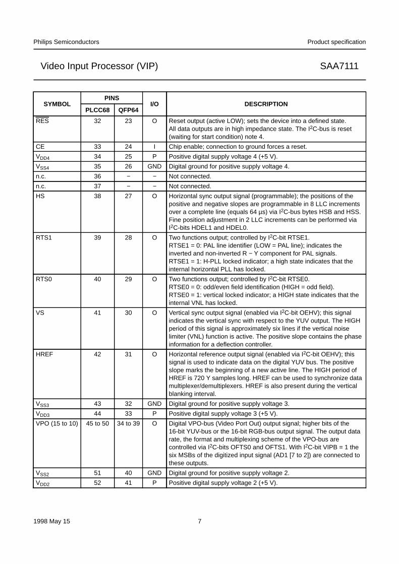
RES 32 23 O Reset output (active LOW); sets the device into a defined state.All data outputs are in high impedance state. The I2C-bus is reset(waiting for start condition) note 4.
CE 33 24 I Chip enable; connection to ground forces a reset.
VDD4 34 25 P Positive digital supply voltage 4 (+5 V).
VSS4 35 26 GND Digital ground for positive supply voltage 4.
n.c. 36 − − Not connected.
n.c. 37 − − Not connected.
HS 38 27 O Horizontal sync output signal (programmable); the positions of thepositive and negative slopes are programmable in 8 LLC incrementsover a complete line (equals 64 µs) via I2C-bus bytes HSB and HSS.Fine position adjustment in 2 LLC increments can be performed viaI2C-bits HDEL1 and HDEL0.
RTS1 39 28 O Two functions output; controlled by I2C-bit RTSE1.RTSE1 = 0: PAL line identifier (LOW = PAL line); indicates theinverted and non-inverted R − Y component for PAL signals.RTSE1 = 1: H-PLL locked indicator; a high state indicates that theinternal horizontal PLL has locked.
RTS0 40 29 O Two functions output; controlled by I2C-bit RTSE0.RTSE0 = 0: odd/even field identification (HIGH = odd field).RTSE0 = 1: vertical locked indicator; a HIGH state indicates that theinternal VNL has locked.
VS 41 30 O Vertical sync output signal (enabled via I2C-bit OEHV); this signalindicates the vertical sync with respect to the YUV output. The HIGHperiod of this signal is approximately six lines if the vertical noiselimiter (VNL) function is active. The positive slope contains the phaseinformation for a deflection controller.
HREF 42 31 O Horizontal reference output signal (enabled via I2C-bit OEHV); thissignal is used to indicate data on the digital YUV bus. The positiveslope marks the beginning of a new active line. The HIGH period ofHREF is 720 Y samples long. HREF can be used to synchronize datamultiplexer/demultiplexers. HREF is also present during the verticalblanking interval.
VSS3 43 32 GND Digital ground for positive supply voltage 3.
VDD3 44 33 P Positive digital supply voltage 3 (+5 V).
VPO (15 to 10) 45 to 50 34 to 39 O Digital VPO-bus (Video Port Out) output signal; higher bits of the16-bit YUV-bus or the 16-bit RGB-bus output signal. The output datarate, the format and multiplexing scheme of the VPO-bus arecontrolled via I2C-bits OFTS0 and OFTS1. With I2C-bit VIPB = 1 thesix MSBs of the digitized input signal (AD1 [7 to 2]) are connected tothese outputs.
VSS2 51 40 GND Digital ground for positive supply voltage 2.
VDD2 52 41 P Positive digital supply voltage 2 (+5 V).
SYMBOLPINS
I/O DESCRIPTIONPLCC68 QFP64

1998 May 15 8
Philips Semiconductors Product specification
Video Input Processor (VIP) SAA7111
Notes
1. For board design without boundary scan implementation (pin compatibility with the SAA7110) connect the TRST pinto ground.
2. This pin provides easy initialization of BST circuit. TRST can be used to force the TAP (Test Access Port) controllerto the Test-Logic-Reset state (normal operation) at once.
3. In accordance with the IEEE1149.1 standard the pads TCK, TDI, TMS and TRST are input pads with an internalpull-up transistor and TDO a 3-state output pad.
4. All pin names that carry an ‘overscore’ have been renamed due to Philips pin name conventions. In previous datasheet versions these pins were marked by the suffix ‘N’, e.g. TRST = TRSTN.
VPO (9 to 0) 53 to 62 42 to 51 O Digital VPO-bus output signal; lower bits of the 16-bit YUV-bus or the16-bit RGB-bus output signal. The output data rate, the format andmultiplexing schema of the VPO-bus are controlled via I2C-bitsOFTS0 and OFTS1. With I2C-bit VIPB = 1 the digitized input signals(AD1 [1 and 0] and AD2 [7 to 0]) are connected to these outputs.
FEI 63 52 I Fast enable input signal (active LOW); this signal is used to controlfast switching on the digital YUV-bus. A HIGH at this input forces theIC to set its Y and UV outputs to the high impedance state; note 4.
GPSW 64 53 O General purpose switch output; the state of this signal is set viaI2C-bus control and the levels are TTL compatible.
XTAL 65 54 O Second output terminal of crystal oscillator; not connected if externalclock signal is used.
XTALI 66 55 I Input terminal for 24.576 MHz crystal oscillator or connection ofexternal oscillator with CMOS compatible square wave clock signal.
VSS1 67 56 GND Digital ground for positive supply voltage 1.
VDD1 68 57 P Positive digital supply voltage 1 (+5 V).
SYMBOLPINS
I/O DESCRIPTIONPLCC68 QFP64

1998 May 15 9
Philips Semiconductors Product specification
Video Input Processor (VIP) SAA7111
Fig.2 Pin configuration (PLCC68).
handbook, full pagewidth
SAA7111
MGC636
10
11
12
13
14
15
16
17
18
19
20
21
22
23
24
25
26
60
59
58
57
56
55
54
53
52
51
50
49
48
47
46
45 VPO15
VPO14
VPO13
VPO12
VPO11
VPO10
VPO9
VPO8
VPO7
VPO6
VPO5
VPO4
VPO3
VPO3
44
27 28 29LL
C
LLC
2
CR
EF
RE
S
CE
HS
VS
RT
S1
RT
S0
HR
EF
n.c.
n.c.
30 31 32 33 34 35 36 37 38 39 40 41 42 43
9 8 7 6 5 4 3 2 1 68 67 66X
TA
LI
XT
AL
TR
ST
TC
K
RT
CO
IICS
A
n.c.
n.c.
n.c.
SD
A
SC
L
GP
SW
FE
I
VP
O0
VP
O1
65 64 63 62 61
n.c.
TDO
TDI
TMS
AI22
AI21
AI12
AI11
AOUT
VSSA2
VD
D1
VS
S1
VDDA2
VSSA1
VDDA1
VSS
VDDA0
VD
D5
VS
S5
VD
D4
VS
S4
VS
S3
VDD3
VSS2
VDD2
VSSA0
VREF

1998 May 15 10
Philips Semiconductors Product specification
Video Input Processor (VIP) SAA7111
Fig.3 Pin configuration (QFP64).
handbook, full pagewidth
SAA7111
MBH226
1
2
3
4
5
6
7
8
9
10
11
12
13
14
15
16
48
47
46
45
44
43
42
41
40
39
38
37
36
35
34
33
17 18 19 20 21 22 23 24 25 26 27 28 29 30 31 32
64 63 62 61 60 59 58 57 56 55 54 53 52 51 50 49
TC
K
IICS
A
SD
A
RT
CO
n.c.
TDO
n.c.
TDI
TMS
VSSA2
AI22
VDDA2
VPO15
VPO14
VPO13
VPO12
VPO11
VPO10
VPO9
VPO8
VPO7
VPO6
VPO5
VPO4
VPO3
VP
O2
VP
O1
VP
O0
FE
I
GP
SW
XT
AL
XT
ALI
VS
S1
VD
D1
VDD3
VDD2
VSS2
AI21
AI11
AOUT
VSSA1
VSSA0
VS
S5
LLC
LLC
2
CR
EF
CE
HS
RT
S1
RT
S0
VS
HR
EF
VS
S3
VS
S4
VD
D4
VR
EF
VSS
VDDA1
VDDA0
VD
D5
AI12
SC
L
TR
ST
RE
S

1998 May 15 11
Philips Semiconductors Product specification
Video Input Processor (VIP) SAA7111
8 FUNCTIONAL DESCRIPTION
8.1 Analog input processing
The SAA7111 offers four analog signal inputs, two analogmain channels with clamp circuit, analog amplifier,anti-alias filter and video CMOS ADC (see Fig.6).
8.2 Analog control circuits
The anti-alias filters are adapted to the line-locked clockfrequency with help from a filter control. During the verticalblanking, time gain and clamping control are frozen.
8.2.1 CLAMPING
The clamp control circuit controls the correct clamping ofthe analog input signals. The coupling capacitor is alsoused to store and filter the clamping voltage. An internaldigital clamp comparator generates the information withrespect to clamp-up or clamp-down. The clamping levelsfor the two ADC channels are fixed for luminance (60) andchrominance (128). Clamping time in normal use is setwith the HCL pulse at the back porch of the video signal.
8.2.2 GAIN CONTROL
Signal (white) peak control limits the gain at signalovershoots. The flow charts (see Figs 10 and 11) showmore details of the AGC. The influence of supply voltagevariation within the specified range is automaticallyeliminated by clamp and automatic gain control.
The gain control circuit receives (via the I2C-bus) the staticgain levels for the two analog amplifiers or controls one ofthese amplifiers automatically via a built-in automatic gain
Fig.4 Analog line with clamp (HCL) and gainrange (HSY).
handbook, halfpage
HCLMGC661HSY
analog line blankingTV line
1
60
225
GAIN CLAMP
control (AGC) as part of the Analog Input Control (AICO).The AGC (automatic gain control for luminance) is used toamplify a CVBS or Y signal to the required signalamplitude, matched to the ADCs input voltage range.The AGC active time is the sync bottom of the video signal.
8.3 Chrominance processing
The 8-bit chrominance signal is fed to the multiplicationinputs of a quadrature demodulator, where two subcarriersignals from the local oscillator DTO1 are applied(0 and 90° phase relationship to the demodulator axis).The frequency is dependent on the present colourstandard. The output signals of the multipliers arelow-pass filtered (four programmable characteristics) toachieve the desired bandwidth for the colour differencesignals.
The colour difference signals are fed to theBrightness/Contrast/Saturation block (BCS), whichincludes the following five functions;
1. AGC (automatic gain control for chrominance)
2. Chroma amplitude matching [different gain factors for(R−Y) and (B−Y) to achieve CCIR-601 levelsCr and Cb]
3. Chroma saturation control
4. Luminance contrast and brightness
5. Limiting YUV to the values 1 (min.) and 254 (max.) tofulfil CCIR-601 requirements.
Fig.5 Automatic gain range.
handbook, halfpageanalog input level
controlledADC input level
maximum
minimum
range 10 dB0 dB 0 dB
MGC660
+4 dB
−6 dB
(1 V(p-p) 75 Ω)

1998 May 15 12
Philips Semiconductors Product specification
Video Input Processor (VIP) SAA7111
The burst processing block provides the feedback loop ofthe chroma PLL and contains;
Burst gate accumulator
Colour identification and killer
Comparison nominal/actual burst amplitude
Loop filter chroma gain control
Loop filter chroma PLL
PAL sequence generation
Increment generation for DTO1 with divider to generatestable subcarrier for non-standard signals.
The chroma comb filter block eliminates crosstalk betweenthe chrominance channels in accordance with the PALstandard requirements. For NTSC colour standards thechroma comb filter can be used to eliminate crosstalk fromluminance to chrominance (cross-colour) for verticalstructures. The comb filter can be switched off if desired.
The resulting signals are fed to the variable Y-delaycompensation, RGB matrix, dithering circuit and outputinterface, which contains the VPO output formatter and theoutput control logic (see Fig.7).
8.4 Luminance processing
The 8-bit luminance signal, a digital CVBS format or aluminance format (S-VHS, HI8), is fed through aswitchable prefilter. High frequency components areemphasized to compensate for loss. The followingchrominance trap filter (f0 = 4.43 or 3.58 MHz centrefrequency selectable) eliminates most of the colour carriersignal, therefore, it must be bypassed for S-video(S-VHS, HI8) signals.
The high frequency components of the luminance signalcan be peaked (control for sharpness improvement viaI2C-bus) in two band-pass filters with selectable transfercharacteristic. This signal is then added to the original(unpeaked) signal. A switchable amplifier achievescommon DC amplification, because the DC gains aredifferent in both chrominance trap modes. The improvedluminance signal is fed to the BCS control located in thechrominance processing block (see Fig.8).
8.5 RGB matrix
Y, Cr and Cb-data are converted after interpolation intoRGB data in accordance with CCIR-601 recommendation.The realized matrix equations consider the digitalquantization:
R = Y + 1.371 Cr
G = Y − 0.336 Cb − 0.698 Cr
B = Y + 1.732 Cb.
After dithering (noise shaping) the RGB data is fed to theoutput interface within the VPO-bus output formatter.
8.6 VPO-bus (digital outputs)
The 16-bit VPO-bus transfers digital data from the outputinterfaces to a feature box or a field memory, a digitalcolour space converter (SAA7192 DCSC), a videoenhancement and digital-to-analog processor(SAA7165 VEDA2) or a colour graphics board(Targa-format) as a graphical user interface.
The output data formats are controlled via the I2C-bus bitsOFTS0, OFTS1 and RGB888. Timing for the data streamformats, 411 YUV (12-bit), 422 YUV (16-bit),565 RGB (16-bit) and 888 RGB (24-bit) with an LLC2 datarate, is achieved by marking each second positive risingedge of the clock LLC in conjunction with CREF (clockreference) (except RGB 888, see special application inFig.27). The higher output signals VPO15 to VPO8 in theYUV format perform the digital luminance signal.The lower output signals VPO7 to VPO0 in the YUV formatare the bits of the multiplexed colour difference signals(B−Y) and (R−Y). The arrangement of the RGB 565 andRGB 888 data stream bits on the VPO-bus is given inTable 5.
The data stream format 422 YUV (the 8 higher outputsignals VPO15 to VPO8) in LLC data rate fulfils theCCIR-656 standard with its own timing reference code atthe start and end of each video data block.
A pixel in the format tables is the time required to transfera full set of samples. In the event of a 4 : 2 : 2 format twoluminance samples are transmitted in comparison to one(B−Y) and one (R−Y) sample within a pixel. The timeframes are controlled by the HREF signal.

1998 May 15 13
Philips Semiconductors Product specification
Video Input Processor (VIP) SAA7111
Fast enable is achieved by setting input FEI to LOW.The signal is used to control fast switching on the digitalVPO-bus. HIGH on this pin forces the YUV outputs to ahigh-impedance state (see Figs 15 and 17).
The digitized analog PAL or NTSC signals AD1 (7 to 0)and AD2 (7 to 0) are connected directly to the VPO-busvia I2C-bit VIPB = 1.
AD1 (7 to 0) → VPO (15 to 8) andAD2 (7 to 0) → VPO (7 to 0)
The selection of the analog input channels are controlledvia I2C-bus subaddress 02 MODE select.
8.7 Synchronization
The prefiltered luminance signal is fed to thesynchronization stage. Its bandwidth is reduced to 1 MHzin a low-pass filter. The sync pulses are sliced and fed tothe phase detectors where they are compared with thesub-divided clock frequency. The resulting output signal isapplied to the loop filter to accumulate all phasedeviations. Internal signals (e.g. HCL and HSY) aregenerated in accordance with analog front-endrequirements. The output signals HS, VS, and PLIN arelocked to the timing reference, guaranteed between theinput signal and the HREF signal, as further improvementsto the circuit may change the total processing delay. It istherefore not recommended to use them for applicationswhich require absolute timing accuracy on the inputsignals. The loop filter signal drives an oscillator togenerate the line frequency control signal LFCO(see Fig.8).
8.8 Clock generation circuit
The internal CGC generates all clock signals required forthe video input processor. The internal signal LFCO is adigital-to-analog converted signal provided by thehorizontal PLL. It is the multiple of the line frequency(6.75 MHz = 432 × fh). Internally the LFCO signal ismultiplied by a factor of 2 or 4 in the PLL circuit (includingphase detector, loop filtering, VCO and frequency divider)to obtain the LLC and LLC2 output clock signals.The rectangular output clocks have a 50% duty factor(see Fig.22).
8.9 Power-on reset and CE input
A missing clock, insufficient digital or analog VDDA0 supplyvoltages (below 3.5 V) will initiate the reset sequence; alloutputs are forced to 3-state. The indicator output RES isLOW for approximately 128 LLC after the internal resetand can be applied to reset other circuits of the digital TVsystem.
It is possible to force a reset by pulling the CE(chip enable) to ground. After the rising edge of CE andsufficient power supply voltage, the outputs LLC, LLC2,CREF, RTCO, RTS0, RTS1, GPSW and SDA return from3-state to active, while HREF, VREF, HS and VS remain in3-state and have to be activated via I2C-bus programming(see Table 4).
8.10 RTCO output
The real time control and status output signal containsserial information about the actual system clock(increment of the HPLL), subcarrier frequency [incrementand phase (via reset) of the FSC-PLL] and PAL sequencebit. The signal can be used for various applications inexternal circuits, e.g. in a digital encoder to achieve cleanencoding (see Fig.16).
8.11 The Line-21 text slicer
The text slicer block detects and acquires Line-21 closedcaptioning data from a 525-line CVBS signal. Extendeddata services on Line-21 Field 2 are also supported.If valid data is detected the two data bytes are stored in twoI2C-bus registers. A parity check is also performed and theresult is stored in the MSB of the corresponding byte.A third I2C-bus register is provided for data valid and dataready flags. The two bits F1VAL and F2VAL indicate thatthe input signal carries valid Closed Captioning data on thecorresponding fields. The data ready bits F1RDY andF2RDY have to be evaluated if asynchronous I2C-busreading is used.
8.11.1 SUGGESTIONS FOR I2C-BUS INTERFACE OF THE
DISPLAY SOFTWARE READING LINE-21 DATA
There are two methods by which the software can acquirethe data;
1. Synchronous reading once per frame (or once perfield): It can use either the rising edge (Line-21 Field 1)or both edges (Line-21 Field 1 or 2) of the ODD signal(pin RTSO) to initiate an I2C-bus read transfer of thethree registers 1A, 1B and 1C
2. Asynchronous reading: It can poll either the F1RDY bit(Line-21 Field 1) or both F1RDY/F2RDY bits (Line-21Field 1 or 2). After valid data has been read thecorresponding F*RDY bit is set to LOW until new datahas arrived. The polling frequency has to be slightlyhigher than the frame or field frequency, respectively.

1998M
ay15
14
Philips S
emiconductors
Product specification
Video Input P
rocessor (VIP
)S
AA
7111
This text is here in white to force landscape pages to be rotated correctly when browsing through the pdf in the Acrobat reader.This text is here in_white to force landscape pages to be rotated correctly when browsing through the pdf in the Acrobat reader.This text is here inThis text is here inwhite to force landscape pages to be rotated correctly when browsing through the pdf in the Acrobat reader. white to force landscape pages to be ...
hand
book
, ful
l pag
ewid
th
AI22
AI21
FUSE (1 : 0)
AI12
AI11
FUSE (1 : 0)
AOSL (1 : 0)
HOLDG
ANALOGCONTROL
GAI10-GAI18
VSSS
n.c.
VBSL 8 8
64
13
MGC655
14
CHRLUM
VERTICALBLANKINGCONTROL
SOURCESWITCH
CLAMPCIRCUIT
ANALOGAMPLIFIER
ANTI-ALIASFILTER
BYPASSSWITCH
SOURCESWITCH
CLAMPCIRCUIT
ANALOGAMPLIFIER
ANTI-ALIASFILTER
BYPASSSWITCH
ADC2
ADC1
TEST
ANDSELECTOR
CLAMPCONTROL
GAINCONTROL
CROSS MULTIPLEXER
ANTI-ALIASCONTROL
VDDA1
VSSA2
AOUT
MODECONTROL
MODE 0MODE 1MODE 2
GAI20-GAI28GUDL0-GUDL2
GAFIXWPOFF
HSY VBLNKSVREF
HCL
AD1BYPAD2BYP
BUFFER
DAC9
DAC9
HLNRSUPTCV
VDDA2
9
5
6
8
11
7
10
12
VSSA1
GLIMBGLIMTWIPASLTCA
Fig.6 Analog input processing.
The pin numbers given in parenthesis refer to the 64-pin package.

1998M
ay15
15
Philips S
emiconductors
Product specification
Video Input P
rocessor (VIP
)S
AA
7111
This text is here in white to force landscape pages to be rotated correctly when browsing through the pdf in the Acrobat reader.This text is here in_white to force landscape pages to be rotated correctly when browsing through the pdf in the Acrobat reader.This text is here inThis text is here inwhite to force landscape pages to be rotated correctly when browsing through the pdf in the Acrobat reader. white to force landscape pages to be ...
hand
book
, ful
l pag
ewid
th
CHRLUM
CODE
AD1BYPAD2BYP
BRIGCONTSATN
HUEC
DCCF
MGC645
VDD1-5
VSS1-5
(57,41,33,25,18)
68,52,44,34,27
(56,40,32,26,19)67,51,43,35,28
(31) 42
(60) 3
(34 to 39),45 to 50
(42 to 51),53 to 62
(52) 63QUADRATURE
DEMODULATOR
COMBFILTERS
FORMATTEROUTPUT
AND INTERFACE
ACCUMULATORBURST GATE
LOW-PASS
LOOP FILTER
SUBCARRIER INCREMENTGENERATION
SUBCARRIERGENERATION
DIVIDER
FCTCCSTD 1
RGB MATRIXinterpolation
dithering
DIT CBR
CHBW0CHBW1
CSTD 0INCS
RES
TCKTDI
2 (59)12 (3)
32 (23)CONTROL
POWER-ON
CONTROLTEST
BLOCK
TDO
TRST
11 (2)
1 (58)
TMS 13 (4)
LUM Y
RTCO
n.c. 10 (1)
CLOCKSCE
Y
UV
RGB
FEI
HREF
VPO(9 : 0)
VPO(15 : 10)
AND
PHASEDEMOD.
AMPLITUDEDETECTOR
OFTS0OFTS1RGB888OEYCOEHVFECOVRLN
GPSWRTSE1RTSE0VIPBVLOFCOLOCOMPO
BRIGHTNESS,CONTRAST,
ANDSATURATION
CONTROL
GAINCONTROL
AND Y-DELAYCOMPENSATION
Fig.7 Chrominance circuit.
The pin numbers given in parenthesis refer to the 64-pin package.

1998M
ay15
16
Philips S
emiconductors
Product specification
Video Input P
rocessor (VIP
)S
AA
7111
This text is here in white to force landscape pages to be rotated correctly when browsing through the pdf in the Acrobat reader.This text is here in_white to force landscape pages to be rotated correctly when browsing through the pdf in the Acrobat reader.This text is here inThis text is here inwhite to force landscape pages to be rotated correctly when browsing through the pdf in the Acrobat reader. white to force landscape pages to be ...
hand
book
, ful
l pag
ewid
th
CREFLLC
XTALI
XTAL
VREFRTS0 HSVSSDASCLIICSA
GPSW
I C BUS CONTROL
CLOCKS
SYNCHRONIZATION CIRCUIT
PREF BYPS APER0APER1VBLB
AUFDHSBHSSFSELVTRC STTCFIDT
VNOI0VNOI1VTRC VTRC
CE
RTS1
MGC654
LLC2
HLCK
VDDA0VSSA0
53
61 63 62 30 29 17 27 28
1624
15
54
55
222021
DAC6
ANDWEIGHTING
ADDINGBAND-PASSVARIABLE
FILTER
CHROMINANCETRAP
PREFILTER
AMPLIFIERMATCHING
CLOCKLINE-LOCKED
GENERATOR
2LOOP FILTER
DETECTORPHASE
COARSE
DETECTORPHASE
FINESYNC SLICER
SYNCPREFILTER
LINE 21TEXT
SLICER
CLOCKCRYSTAL
GENERATORTIME
DISCRETE
OSCILLATOR 2INTERFACEI C-BUS
PROCESSORVERTICAL COUNTER
GENERATIONCLOCK
CIRCUIT
LUMINANCE CIRCUIT
BPSS0BPSS1PREF
LUM
VBLB
VBLB
Y
CLOCK CIRCUIT
INCS
STAGE
HPLLVTRCEXFIL
BYTE1BYTE2
STATUS2
2
Fig.8 Luminance and sync processing.
The pin numbers given in parenthesis refer to the 64-pin package.

1998 May 15 17
Philips Semiconductors Product specification
Video Input Processor (VIP) SAA7111
9 GAIN CHARTS
Fig.9 Amplifier curve.
handbook, halfpage
0
7.5
5.5
dB
3.5
1.5
−0.5
−4.5
−2.5
256 512gain value (i)
MGC648
bit [8] = 1
factor dB = 20 x log10 gain =( 512
768 − i
i > 256
bit [8] = 0
factor dB = 20 x log10 gain =( 512257 + i (
i < 256
(
Fig.10 Clamp and gain flow.
WIPE = white peak level (254); SBOT = sync bottom level (1); CLL = clamp level [60 Y (128 C)];HSY = horizontal sync pulse; HCL = horizontal clamp pulse.
handbook, full pagewidth
1 0
+ CLAMP − CLAMP NO CLAMP
1 0 1 0
0 1 1 0
MGC647
fast − GAIN slow + GAIN+ GAIN − GAIN
HCL HSY
ADC
SBOT WIPECLL
ANALOG INPUT
GAIN -><- CLAMP
VBLKNO BLANKING ACTIVE1 0
1998 May 15 18
Philips Semiconductors Product specification
Video Input Processor (VIP) SAA7111
handbook, full pagewidth ANALOG INPUT
AMPLIFIER
ANTI-ALIAS FILTER
ADC
LUMA/CHROMA DECODER
X
HSY
>254
>254
<1<4
>248
X = 0 X = 1
−1/LLC2 +1/LLC2 −1/LLC2 +/− 0+1/F +1/L
GAIN ACCUMULATOR (18 BITS)
ACTUAL GAIN VALUE 9-BIT (AGV) [−6/+6 dB]
X
STOP
HSY
Y
UPDATE FGV
MGC652
AGV
GAIN VALUE 9-BIT
1 0
1 0
1 0
1 0
1 0
1 0
1 0
1 0
01
10
10
VBLK1 0NO ACTION
9
8
DACgain
HOLDG
Fig.11 Gain flow chart.
X = system variable; Y = AGV − FGVI > GUDL; VBLK = vertical blanking pulse;HSY = horizontal sync pulse; AGV = actual gain value; FGV = frozen gain value.

1998 May 15 19
Philips Semiconductors Product specification
Video Input Processor (VIP) SAA7111
10 LIMITING VALUESIn accordance with the Absolute Maximum Rating System (IEC 134).
Note
1. Human body model: equivalent to discharging a 100 pF capacitor through a 1.5 kΩ resistor.
11 CHARACTERISTICSVDDD = 4.5 to 5.5 V; VDDA = 4.75 to 5.25 V; Tamb = 25 °C; unless otherwise specified.
SYMBOL PARAMETER CONDITIONS MIN. MAX. UNIT
VDDD digital supply voltage −0.5 +6.5 V
VDDA analog supply voltage −0.5 +6.5 V
Vdiff voltage difference between VSSAall andVSSall
− 100 mV
Tstg storage temperature −65 +150 °CTamb operating ambient temperature 0 70 °CTamb(bias) operating ambient temperature under bias −10 +80 °CVESD electrostatic discharge all pins note 1 −2000 +2000 V
SYMBOL PARAMETER CONDITIONS MIN. TYP. MAX. UNIT
Supplies
VDDD digital supply voltage 4.5 5.0 5.5 V
IDDD digital supply current 100 130 160 mA
PD digital power 0.45 0.65 0.88 W
VDDA analog supply voltage 4.75 5.0 5.25 V
IDDA analog supply current 60 70 80 mA
PA analog power 0.32 0.35 0.38 W
PA+D analog and digital power 0.77 1.0 1.26 W
Analog part
Iclamp clamping current VI = 1.25 V DC − 2 − µA
Vi(p-p) input voltage (peak-to-peakvalue), AC coupling required
couplingcapacitor = 10 nF; note 1
0.55 1.0 1.5 V
|Zi| input impedance clamping current off 200 − − kΩCi input capacitance − − 10 pF
αcs channel crosstalk fi = 5 MHz − −50 − dB
Analog-to-digital converters
B bandwidth at −3 dB − 15 − MHz
φdiff differential phase (amplifierplus anti-alias filter = bypass)
− 2 − deg
Gdiff differential gain (amplifier plusanti-alias filter = bypass)
− 2 − %
fADC ADC clock frequency 11 − 16 MHz
DLE DC differential linearity error − 0.5 − LSB
ILE DC integral linearity error − 1 − LSB

1998 May 15 20
Philips Semiconductors Product specification
Video Input Processor (VIP) SAA7111
Digital inputs
VIL LOW-level input voltage pinsSDA and SCL
−0.5 − +1.5 V
VIH HIGH-level input voltage pinsSDA and SCL
0.7VDDD − VDDD + 0.5 V
VIL(xtalI) LOW-level CMOS inputvoltage pin XTALI
− − 0.3VDDD V
VIH(xtalI) HIGH-level CMOS inputvoltage pin XTALI
0.7VDDD − − V
VILn LOW-level input voltage allother inputs
−0.5 − +0.8 V
VIHn HIGH-level input voltage allother inputs
2.0 − VDDD + 0.5 V
ILI input leakage current − − 1 µA
Ci(I/O) input capacitance inputs and outputs athigh-impedance
− − 8 pF
Ci(n) input capacitance all otherinputs
− − 8 pF
Digital outputs
VOL LOW-level output voltage pinsSDA and SCL
SDA/SCL at 3 mA sinkcurrent
− − 0.4 V
VOL LOW-level output voltage note 2 0 − 0.6 V
VOH HIGH-level output voltage note 2 2.4 − VDDD V
VOL(clk) LOW-level output voltage forclocks
−0.5 − +0.6 V
VOH(clk) HIGH-level output voltage forclocks
2.6 − VDDD + 0.5 V
FEI input timing
tSU;DAT input data set-up time 13 − − ns
tHD;DAT input data hold time 3 − − ns
Data and control output timing
CL output load capacitance 15 − 50 pF
tOHD;DAT output hold time CL = 15 pF 5 − − ns
tPD propagation delay CL = 40 pF − − 21 ns
tPDZ propagation delay to 3-state − − 21 ns
SYMBOL PARAMETER CONDITIONS MIN. TYP. MAX. UNIT

1998 May 15 21
Philips Semiconductors Product specification
Video Input Processor (VIP) SAA7111
Clock output timing (LLC and LLC2)
CL(LLC) output load capacitance 15 − 40 pF
Tcy cycle time LLC 35 − 39 ns
LLC2 70 − 78 ns
δLLC duty factors for tLLCH/tLLC andtLLC2H/tLLC2
CL = 40 pF 40 − 60 %
tr rise time Vi = 0.6 to 2.6 V − − 5 ns
tf fall time Vi = 2.6 to 0.6 V − − 5 ns
tdLLC2 delay time LLC output to LLC2output
Vi = 1.5 V;LLC/LLC2 = 40 pF
−1 − +1 ns
Data qualifier output timing (CREF)
tOHD;CREF output hold time CL = 15 pF 4 − − ns
tPD;CREF propagation delay frompositive edge of LLC
CL = 40 pF − − 20 ns
Clock input timing (XTALI)
δXTALI duty factor for tXTALIH/tXTALI nominal frequency 40 − 60 %
Horizontal PLL
fHn nominal line frequency 50 Hz field − 15625 − Hz
60 Hz field − 15734 − Hz
∆fH/fHn permissible static deviation − − 5.7 %
Subcarrier PLL
fSCn nominal subcarrier frequency PAL BGHI and NTSC 443 − 4433619 − Hz
NTSC M − 3579545 − Hz
PAL M − 3575612 − Hz
PAL N − 3582056 − Hz
∆fSCH/fSCHn lock-in range ±400 − − Hz
SYMBOL PARAMETER CONDITIONS MIN. TYP. MAX. UNIT

1998 May 15 22
Philips Semiconductors Product specification
Video Input Processor (VIP) SAA7111
Notes
1. The levels must be measured with load circuits; 1.2 kΩ at 3 V (TTL load); CL = 50 pF.
2. The effects of rise and fall times are included in the calculation of tOHD;DAT, tPD and tPDZ. Timings and levels refer todrawings and conditions illustrated in Figs 12 and 13.
Table 1 Processing delay
Crystal oscillator
fn nominal frequency 3rd harmonic − 24.576 − MHz
∆f/fn permissible nominalfrequency deviation
− − ±50 10−6
∆f/fn(T) permissible nominalfrequency deviation withtemperature
− − ±20 10−6
CRYSTAL SPECIFICATION (X1)
TambX1 operating ambienttemperature
0 − 70 °C
CL load capacitance 8 − − pF
Rs series resonance resistor − 40 80 ΩC1 motional capacitance − 1.5 ±20% − fF
C0 parallel capacitance − 3.5 ±20% − pF
FUNCTIONTYPICAL ANALOG DELAYAI22 −> ADCIN (AOUT) (ns)
DIGITAL DELAYADCIN → VPO (LLC-CLOCKS)
[YDEL(2 to 0) = 000]
Without amplifier or anti-alias filter 14
139With amplifier, without anti-alias filter 30
With amplifier plus anti-alias filter 72
SYMBOL PARAMETER CONDITIONS MIN. TYP. MAX. UNIT

1998 May 15 23
Philips Semiconductors Product specification
Video Input Processor (VIP) SAA7111
12 TIMING DIAGRAMS
Fig.12 Clock/data timing (8-bit CCIR-656 format of the VPO-bus).
An explanation of the output formats is given in Table 5.
handbook, full pagewidth
2.4 V
tLLC
tf
tPDtOHD;DAT
tLLCL
tLLCH
OUTPUTS VPO, HREF,VREF, VS, HS
CLOCK OUTPUT LLC
tr
0.6 V
2.6 V1.5 V0.6 V
MGC658
Fig.13 Clock/data timing (12/16-bit CCIR-601 format of the VPO-bus).
An explanation of the output formats is given in Table 5. The FEI timing of the VPO-bus is illustrated in Figs 15 and 17.
handbook, full pagewidth
2.4 V0.6 V
tLLC
tf
tPD
tOHD;CREF
tdLLC2
tr
tLLCL
tLLCH
2.4 V0.6 V
OUTPUTS VPO, HREF,
CLOCK OUTPUT LLC
CLOCK OUTPUT LLC2
1.5 V0.6 V
2.6 V
1.5 V0.6 V
2.6 V
VREF, VS, HS
OUTPUT CREF
tOHD;DAT
tdLLC2
tPD
MGC659
tLLC
tPD
tOHD;CREF
1998 May 15 24
Philips Semiconductors Product specification
Video Input Processor (VIP) SAA7111
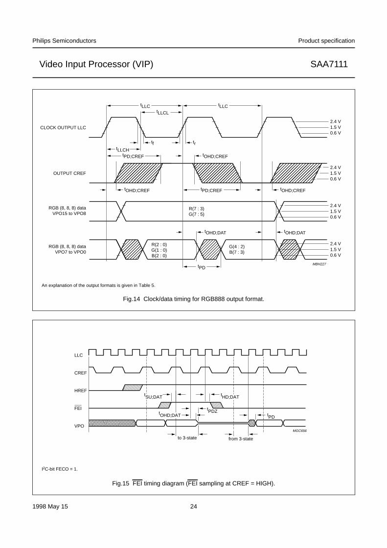
Fig.14 Clock/data timing for RGB888 output format.
An explanation of the output formats is given in Table 5.
handbook, full pagewidth
MBH227
2.4 V1.5 V0.6 V
2.4 V1.5 V0.6 V
2.4 V1.5 V0.6 V
CLOCK OUTPUT LLC
OUTPUT CREF
RGB (8, 8, 8) dataVPO15 to VPO8
RGB (8, 8, 8) dataVPO7 to VPO0
2.4 V1.5 V0.6 V
tOHD;DATtOHD;DAT
tOHD;CREF tOHD;CREF
tOHD;CREF
tPD;CREF
tPD
tPD;CREF
R(7 : 3)G(7 : 5)
G(4 : 2)B(7 : 3)
R(2 : 0)G(1 : 0)B(2 : 0)
tLLCL
tLLC tLLC
tf trtLLCH
Fig.15 FEI timing diagram (FEI sampling at CREF = HIGH).
I2C-bit FECO = 1.
handbook, full pagewidthLLC
CREF
HREF
FEI
VPO
to 3-state from 3-state
MGC656
tPDZtPD
tHD;DATtSU;DAT
tOHD;DAT

1998 May 15 25
Philips Semiconductors Product specification
Video Input Processor (VIP) SAA7111
Fig.16 Real time control output.
(1) Set to zero for one transmission, if a phase reset of the fsc - DTO is applied via I2C-bit CDTO. RTCO sequence is generated in LLC/4.
The HPLL increment represents the actual LFCO frequency (fLFCO × 4 = fLLC); 16 LSB from 20, upper four bits are fixed to 0100b
Where: fXTAL = 24.576 MHz, word length DTO2 = 20 bits.
The fsc increment represents the actual subcarrier frequency (related to the actual clock); 23 LSB from 24, MSB is 0b.
Where: word length DTO1 = 24 bits.
fLFCO
INCRHPLL fXTAL×
2word length DTO2
-------------------------------------------------=
fsc
INCRFSCPLL fXTAL×
2word length DTO1
-------------------------------------------------------INCRHPLL
219
----------------------------×=
handbook, full pagewidth
TIME SLOT:
BIT NO.:
transmitted once per line
22
1
21 1920 15161718 78911 10121314
SEQUENCE
190 67
2 3
6 45 230
16
45
RE
SE
RV
ED
16
INCRFSCPLL
MGC64963
01
RESERVED
128
HIGH
LOW
15
INCRHPLL
RE
SE
RV
ED
1
68
DTO RESET(1)
50 Hz fields: 23560 Hz fields: 232
Fig.17 FEI timing diagram (FEI sampling at CREF = LOW).
Timing is compatible with SAA7110; I2C-bit FECO = 0.
handbook, full pagewidth LLC
CREF
HREF
VPO
tSU;DAT tHD;DAT
to 3-state
MGC657
from 3-state
tOHD;DAT tPD
tPDZFEI

1998 May 15 26
Philips Semiconductors Product specification
Video Input Processor (VIP) SAA7111
Fig.18 HREF timing diagram.
handbook, full pagewidth
0
LLC
CREF
LLC2
HREF
Yn
UVn
HREF
Yn
UVn
1 2 3 4
U0 V0 U2 V2 U4
END OF ACTIVE LINE
START OF ACTIVE LINE
719718717716715
U718 V718
MGC646
V716U716V714

1998 May 15 27
Philips Semiconductors Product specification
Video Input Processor (VIP) SAA7111
Fig.19 Horizontal timing diagram.
(1) PLIN is switched to output RTS1 via I2C-bit RTSE1 = 0.
(2) See Table 1.
handbook, full pagewidth 0
108 −107
107 −106
MGC664
CVBS
50 x 2/LLC
139 x 1/LLC
7 x 2/LLC
Y - output
HREF (50 Hz)
12 x 2/LLC720 x 2/LLC 144 x 2/LLC
3 x 2/LLC
138 x 2/LLC720 x 2/LLC
burst
RTS1 (PLIN)(1)
processing delay CVBS->VPO(2)
0
0
4/LLC
HREF (60 Hz)
HS (60 Hz)
sync clipped
16 x 2/LLC
HS (50 Hz)programming range(step size: 8/LLC)
HS (60 Hz)programming range(step size: 8/LLC)
HS
113 x 2/LLC

1998 May 15 28
Philips Semiconductors Product specification
Video Input Processor (VIP) SAA7111
Fig.20 Vertical timing diagram for 50 Hz [nominal input signal VNL in normal mode (VNOI = 00b)].
(1) ODD is switched to output RTS0 via I2C-bit RTSE0 = 0.
The luminance peaking and the chrominance trap are bypassed during VREF = 0 if I2C-bit VBLB is set to logic 1.
The chrominance delay line (chroma-comb filter for NTSC, phase error correcting for PAL) is disabled during VREF = 0.
handbook, full pagewidth
313 314 315 316 317 318 319 335 336
1 2 3 4 5 6 7 8 22625
HREF
input CVBS
b: 2nd field
a: 1st field
VREF
VREF
VREF
VREF
VRLN = 1
VRLN = 0
624623622 23
HREF
input CVBS312311310
VRLN = 0
337
MGC662
503 x 2/LLC
VS
RTS0 (ODD)(1)
RTS0 (ODD)(1)
320
VS
71 x 2/LLC
VRLN = 1

1998 May 15 29
Philips Semiconductors Product specification
Video Input Processor (VIP) SAA7111
Fig.21 Vertical timing diagram for 60 Hz [nominal input signal VNL in normal mode (VNOI = 00b)].
(1) ODD is switched to output RTS0 via I2C-bit RTSE0 = 0.
(2) Line numbers in parenthesis refer to CCIR line counting.
The luminance peaking and the chrominance trap are bypassed during VREF = 0 if I2C-bit VBLB is set to logic 1.
The chrominance delay line (chroma-comb filter for NTSC, phase error correcting for PAL) is disabled during VREF = 0.
handbook, full pagewidth
VS
(266) (267) (268) (269) (270) (271) (272) (273) (274)
(4) (5) (6) (7) (8) (9) (10) (11) (20)(3)
HREF
b: 2nd field
a: 1st field
input CVBS
(2)(1)(525) (21) (22)
(283) (284)(265)(264)(263)(262)
VRLN = 1
VRLN = 0
VRLN = 1
VRLN = 0
1 2 3 4 5 6 7 8 17525524523522 18 19
263 264 265 266 267 268 269 270 271 280 281262261260259(285)282
(2)
(2)
MGC663
493 x 2/LLC
RTS0 (ODD)(1)
61 x 2/LLC
VREF
VREF
VREF
VREF
VS
HREF
input CVBS
RTS0 (ODD)(1)

1998 May 15 30
Philips Semiconductors Product specification
Video Input Processor (VIP) SAA7111
Table 2 Digital output control
Notes
1. OFTS(1 : 0) = 10 or 01 or 00.
2. OFTS(1 : 0) = 11.
13 CLOCK SYSTEM
13.1 Clock generation circuit
The internal CGC generates the system clocks LLC, LLC2and the clock reference signal CREF. The internalgenerated LFCO (triangular waveform) is multiplied by2 or 4 via the analog PLL (including phase detector, loopfilter, VCO and frequency divider). The rectangular outputsignals have a 50% duty factor.
OEYC FEIVPO
15 to 0 (1) 15 to 8 (2) 7 to 0 (2)
0 0 Z Z Z
1 0 active active Z
0 1 Z Z Z
1 1 Z active Z
Table 3 Clock frequencies
CLOCK FREQUENCY (MHz)
XTAL 24.576
LLC 27
LLC2 13.5
LLC4 6.75
LLC8 3.375
Fig.22 Block diagram of clock generation circuit.
handbook, full pagewidthBAND PASSFC = LLC/4
ZEROCROSS
DETECTION
PHASEDETECTION
LOOPFILTER
DIVIDER1/2
DIVIDER1/2
OSCILLATOR
DELAY CREF
MGC632
LLC2
LLCLFCO

1998 May 15 31
Philips Semiconductors Product specification
Video Input Processor (VIP) SAA7111
13.2 Power-on control
Power-on reset is activated at power-on, chip enable, PLL clock generation failure and if the supply voltage falls below3.5 V. The RES signal can be applied to reset other circuits of the digital picture processing system.
Fig.23 Power-on control circuit.
andbook, full pagewidth
MGC633128 LCC896 LCC
digital delaysome ms 20 to 200 µs
PLL-delay
<1 ms
RES
LLC
RESINT
LLCINT
XTAL
CE
POC VDDA
POCLOGIC
ANALOG
POC VDDDDIGITAL
POCDELAY
CLOCKPLL
CE
LLC
CLK0
RES
CE = chip enable input; XTAL = crystal oscillator output; LLCINT = internal system clock;
RESINT = internal reset; LLC = line-locked system clock output; RES = reset output (active LOW).

1998 May 15 32
Philips Semiconductors Product specification
Video Input Processor (VIP) SAA7111
Table 4 Power-on control sequence
14 OUTPUT FORMATS
Table 5 Output formats
Notes
1. Values in accordance with CCIR-601.
2. Before and after the video data, video timing codes are inserted in accordance with CCIR-656.
3. Values not defined during HREF = LOW.
4. CREF = 0 (see Fig.14).
5. CREF = 1 (see Fig.14).
INTERNAL POWER-ONCONTROL SEQUENCE
PIN OUTPUT STATUS FUNCTION
Directly after power-onasynchronous reset
VPO15 to VPO0, RTCO, RTS0, RTS1,GPSW, HREF, VREF, HS, VS, LLC, LLC2and CREF are in high-impedance state
direct switching to high impedance for20 to 200 ms
Synchronous resetsequence
LLC, LLC2, CREF, RTCO, RTS0, RTS1,GPSW and SDA become active;VPO15 to VPO0, HREF, VREF, HS and VSare held in high-impedance state
internal reset sequence
Status after power-oncontrol sequence
VPO15 to VPO0, HREF, VREF, HS and VSare held in high-impedance state
after power-on (reset sequence) a completeI2C-bus transmission is required
BUS SIGNAL 411 (12-BIT) 422 (16-BIT) (1) CCIR-656 (8-BIT)(2) RGB (16-BIT) (3) RGB (24-BIT) (3)
VPO15 Y07 Y17 Y27 Y37 Y07 Y17 U07 Y07 V07 Y17 R4 R7 R7VPO14 Y06 Y16 Y26 Y36 Y06 Y16 U06 Y06 V06 Y16 R3 R6 R6VPO13 Y05 Y15 Y25 Y35 Y05 Y15 U05 Y05 V05 Y15 R2 R5 R5VPO12 Y04 Y14 Y24 Y34 Y04 Y14 U04 Y04 V04 Y14 R1 R4 R4VPO11 Y03 Y13 Y23 Y33 Y03 Y13 U03 Y03 V03 Y13 R0 R3 R3VPO10 Y02 Y12 Y22 Y32 Y02 Y12 U02 Y02 V02 Y12 G5 G7 G7VPO9 Y01 Y11 Y21 Y31 Y01 Y11 U01 Y01 V01 Y11 G4 G6 G6VPO8 Y00 Y10 Y20 Y30 Y00 Y10 U00 Y00 V00 Y10 G3 G5 G5VPO7 U07 U05 U03 U01 U07 V07 X X X X G2 G4 R2VPO6 U06 U04 U02 U00 U06 V06 X X X X G1 G3 R1VPO5 V07 V05 V03 V01 U05 V05 X X X X G0 G2 R0VPO4 V06 V04 V02 V00 U04 V04 X X X X B4 B7 G1VPO3 X X X X U03 V03 X X X X B3 B6 G0VPO2 X X X X U02 V02 X X X X B2 B5 B2VPO1 X X X X U01 V01 X X X X B1 B4 B1VPO0 X X X X U00 V00 X X X X B0 B3 B0Pixel order Y 0 1 2 3 0 1 0 1 − note 4 note 5Pixel order UV 0 0 0 − −Data rates LLC2 LLC2 LLC LLC2 LLCI2C-buscontrol signals
OFTS0 = 0 OFTS0 = 1 OFTS0 = 1 OFTS0 = 0 OFTS0 = 0OFTS1 = 1 OFTS1 = 0 OFTS1 = 1 OFTS1 = 0 OFTS1 = 0
RGB888 = X RGB888 = X RGB888 = X RGB888 = 0 RGB888 = 1

1998 May 15 33
Philips Semiconductors Product specification
Video Input Processor (VIP) SAA7111
Fig.24 VPO output signal range with default BCS settings.
Equations for modification to the YUV levels via BCS control I2C bytes BRIG, CONT and SATN.
Luminance:
Chrominance:
It should be noted that the resulting levels are limited to 1 to 254 in accordance with CCIR-601/656 standard.
YOUT Int CONT71
------------------ Y 128–( )× BRIG+=
UVOUT Int SATN64
----------------- Cr Cb, 128–( )× 128+=
handbook, full pagewidth
LUMINANCE 100%
+255
+235
+128
+16
0
white
black
U-COMPONENT
+255+240
+212 +212
+128
+16
+44
0
blue 100%
blue 75%
yellow 75%
yellow 100%
colourless
V-COMPONENT
+255+240
+128
+16
+44
0
red 100%
red 75%
cyan 75%
cyan 100%
colourless
MGC634
a. Y output range. b. U output range (Cb). c. V output range (Cr).
CCIR Rec. 602 digital levels.
Fig.25 Oscillator application.
handbook, full pagewidth
XTAL
XTALI
65 (54)
66 (55)
MGC635
XTAL
L = 10 µH ±20%
C =10 pF
C =10 pF
C =1 nF
quartz (3rd harmonic)24.576 MHz
XTALI
65 (54)
66 (55)
SAA7111 SAA7111
The pin numbers given in parenthesis refer to the 64-pin package.
a. With quartz crystal. b. With external clock.
1998 May 15 34
Philips Semiconductors Product specification
Video Input Processor (VIP) SAA7111
15 APPLICATION INFORMATION
handbook, full pagewidth
Q1(24.576 MHz)
VPO(15 : 0)
SCL
VDDD
AI22
FEI
SDARTCO
VS
HS
AOUT
GPSW
RTS0
RTS1
RES
CREF
LLC2
LLC
HREF
VSSVSSVSSA
VDDA
VSSA
VDD
VSS
VSS
VREF
VSS
SAA7111
R4
75 Ω
C4
10 nF
C7
100 nF
100 nF
100 nF
100 nFC8
C9
C11
C12
C13
C14
C15
R6 1 kΩ
n.c.n.c.V
SS
A2
VS
S
VS
S1
VS
S2
VS
S3
VS
S4
VS
S5
IICS
A
VS
SA
1
VS
SA
0V
DD
A0
VD
DA
1V
DD
A2
VD
D1
VD
D2
VD
D3
VD
D4
VD
D5
TM
S
TD
I
TD
O
TC
K
TR
ST
n.c.
C17
L110µH
C16
1 nF 10 pF 10 pF
C18
R5
1 kΩ
27(18)
34(25)
44(33)
52(41)
68(57)
12(3)
16(7)
20(11)
24(15)
(34) 45
(35) 46
(36) 47
(37) 48
(38) 49
(39) 50
(42) 53
(43) 54
(44) 55
(45) 56
(46) 57
(47) 58
(48) 59
(31) 42
(27) 38
(30) 41
(60) 3
(14) 23
(53) 64
(28) 39
(29) 40
(20) 29
(21) 30
(22) 31
(23) 32
(17) 26
36 3798(64)
7
1(58)
2(59)
(61)4
(19)28
(26)35
(32)43
(40)51
(56)67
(13)22
(5)14
(9)18 10
(16)25
11(2)
13(4)
15 (6)
6 (63)
5 (62)
63 (52)
33 (24)
66 (55)
65 (54)XTAL
XTALI
n.c.n.c.
MGC651
VSSA
BSTVSS
n.c.n.c.
n.c.
n.c.
(49) 60
(50) 61
(51) 62
100 nF
100 nF
100 nF
100 nF
R3
75 Ω
C3
10 nF
VSSA
AI21
R2
75 Ω
C2
10 nF
VSSA
17 (8)
AI12
R1
75 Ω
C1
10 nF
VSSA
19 (10)
AI11 21 (12)
15
14
13
12
11
10
9
8
7
6
5
4
3
2
1
0
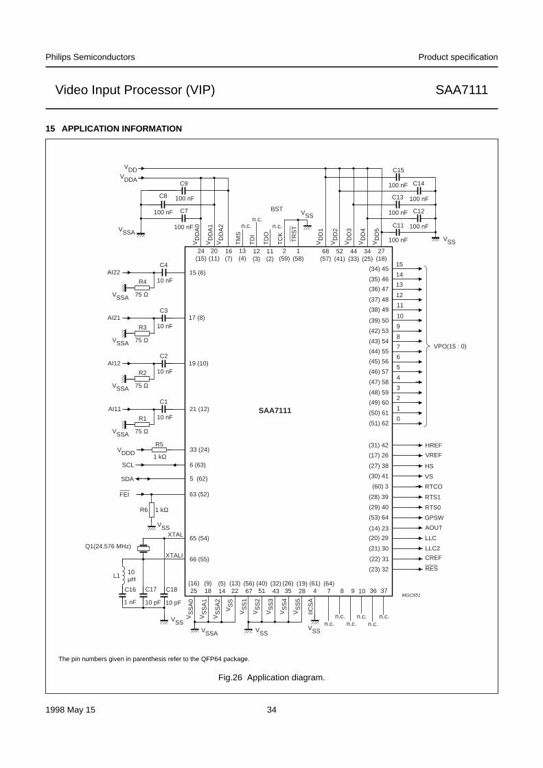
Fig.26 Application diagram.
The pin numbers given in parenthesis refer to the QFP64 package.

1998 May 15 35
Philips Semiconductors Product specification
Video Input Processor (VIP) SAA7111
Fig.27 Application diagram for RGB 24-bit output format.
The pin numbers given in parenthesis refer to the QFP64 package.
I2C-bus control bits:
OFTS(1 : 0) = 00 (subaddress 10h, bits D7 and D6).
RGB888 = 1 (subaddress 12h, bit D3).
handbook, full pagewidth
OEN
D77
6
5
4
3
2
1
0
D6
D5
D4 e.g.74HCT574D3
D2
D1
D0
(44) 55
(45) 56
(46) 57
(47) 58
(48) 59
(49) 60
(50) 61
(51) 62
(31) 42 HREF
(17) 26
(27) 38
(30) 41
(60) 3
(28) 39
(29) 40
(53) 64
(14) 23
(20) 29
(21) 30
(32) 31
(23) 32
VSSVSS
VSS
CLK
O73
R (2 : 0)R (7 : 0)
O6
O5
O4
O3
O2
O1
00
VDD VDD
3
3
3
2G (1 : 0)
G (7 : 0)
3B (2 : 0)
B (7 : 0)
LLC2N
MGD137
LLC2
e.g. 74F240
B (7 : 3)VPO (4 : 0)
VPO(7 : 0)
SAA7111
VPO (15 : 11) R (7 : 3)
G (7 : 5)
G (4 : 2)
VPO (10 : 8)
VPO (7 : 5)
5
8
8
VREF
HS
VS
RTCO
RTS1
RTS0
GPSW
AOUT
LLC
CREF
RES
8
15
14
13
12
11
10
9
8
(34) 45
(35) 46
(36) 47
(37) 48
(38) 49
(39) 50
(42) 53
(43) 54
VPO(15 : 8)
15.1 Layout hints
Use separate ground planes for analog and digital ground.Connect these planes at one point directly under thedevice, by using a zero Ω resistor. Use separate supplylines for analog and digital supply. Place the supplydecoupling capacitors nearby the supply pins.
Place the coupling (clamp) capacitors close to the analoginput pins. Place the termination resistors close to thecoupling capacitors. Care should be exercised concerningthe hidden layout capacitors around the crystalapplication. To avoid reflection effects use serial resistorsin the clock, sync and data lines.

1998 May 15 36
Philips Semiconductors Product specification
Video Input Processor (VIP) SAA7111
16 I2C-BUS DESCRIPTION
16.1 I2C-bus format
Table 6 Write procedure
Table 7 Read procedure (combined format)
Table 8 Description of I2C-bus format
Notes
1. If more than one byte DATA is transmitted then the auto-increment of the subaddress is performed.
2. During slave transmitter mode the SCL-LOW period may be extended by pulling SCL to LOW (in accordance withthe I2C-bus specification).
3. The I2C-bus subaddress 00 has to be initialized with 0 before being read.
S SLAVE ADDRESS W ACK(s) SUBADDRESS ACK(s) DATA (N BYTES) ACK(s) P
S SLAVE ADDRESS W ACK(s) SUBADDRESS ACK(s)
Sr SLAVE ADDRESS R ACK(s) DATA (N BYTES) ACK(m) P
CODE DESCRIPTION
S START condition
Sr repeated START condition
Slave address W 0100 1000b (IICSA = LOW) or 0100 1010b (IICSA = HIGH)
Slave address R 0100 1001b (IICSA = LOW) or 0100 1011b (IICSA = HIGH)
ACK(s) acknowledge generated by the slave
ACK(m) acknowledge generated by the master
Subaddress subaddress byte; see Table 9
Data data byte, see; note 1 and Table 9
P STOP condition
X = LSB slaveaddress
read/write control bit; X = 0, order to write (the circuit is slave receiver); X = 1, order to read(the circuit is slave transmitter)
Slave address read = 49H or 4BH; note 2
write = 48H or 4AH
IICSA = 0 or 1
Subaddress 00H chip version read and write; note 3
01H reserved −02H to 05H front-end part read and write
06H to 12H decoder part read and write
13H to 19H reserved −1AH to 1CH Line-21 text slicer part read only
1DH to 1EH reserved −1FH status byte read only

1998 May 15 37
Philips Semiconductors Product specification
Video Input Processor (VIP) SAA7111
Table 9 I2C-bus receiver/transmitter overview
Note
1. All unused control bits must be programmed with 0.
16.2 I2C-bus detail
The I2C-bus receiver slave address is 48H/49H. Subaddresses 0F, 1D, 1E and 13 to 19 are reserved; subaddress 01 isreserved for chip version.
SLAVE ADDRESSREAD WRITE IICSA
49H and 4BH 48H and 4AH 0 and 1
REGISTERFUNCTION
SUB-ADDR.
D7 D6 D5 D4 D3 D2 D1 D0
Chip version 00 ID07 ID06 ID05 ID04 ID03 ID02 ID01 ID00
Reserved 01 (1) (1) (1) (1) (1) (1) (1) (1)
Analog input control 1 02 FUSE1 FUSE0 GUDL2 GUDL1 GUDL0 MODE2 MODE1 MODE0
Analog input control 2 03 (1) HLNRS VBSL WPOFF HOLDG GAFIX GAI28 GAI18
Analog input control 3 04 GAI17 GAI16 GAI15 GAI14 GAI13 GAI12 GAI11 GAI10
Analog input control 4 05 GAI27 GAI26 GAI25 GAI24 GAI23 GAI22 GAI21 GAI20
Horizontal sync start 06 HSB7 HSB6 HSB5 HSB4 HSB3 HSB2 HSB1 HSB0
Horizontal sync stop 07 HSS7 HSS6 HSS5 HSS4 HSS3 HSS2 HSS1 HSS0
Sync control 08 AUFD FSEL EXFIL (1) VTRC HPLL VNOI1 VNOI0
Luminance control 09 BYPS PREF BPSS1 BPSS0 VBLB UPTCV APER1 APER0
Luminance brightness 0A BRIG7 BRIG6 BRIG5 BRIG4 BRIG3 BRIG2 BRIG1 BRIG0
Luminance contrast 0B CONT7 CONT6 CONT5 CONT4 CONT3 CONT2 CONT1 CONT0
Chroma saturation 0C SATN7 SATN6 SATN5 SATN4 SATN3 SATN2 SATN1 SATN0
Chroma Hue control 0D HUEC7 HUEC6 HUEC5 HUEC4 HUEC3 HUEC2 HUEC1 HUEC0
Chroma control 0E CDTO CM99 CSTD1 CSTD0 DCCF FCTC CHBW1 CHBW0
Reserved 0F (1) (1) (1) (1) (1) (1) (1) (1)
Format/delay control 10 OFTS1 OFTS0 HDEL1 HDEL0 VRLN YDEL2 YDEL1 YDEL0
Output control 1 11 GPSW (1) FECO COMPO OEYC OEHV VIPB COLO
Output control 2 12 RTSE1 RTSE0 (1) CBR RGB888 DIT AOSL1 AOSL0
Reserved 13-19 (1) (1) (1) (1) (1) (1) (1) (1)
Text slicer status 1A (1) (1) (1) (1) F2VAL F2RDY F1VAL F1RDY
Decoded bytes of thetext slicer
1B P1 BYTE16 BYTE15 BYTE14 BYTE13 BYTE12 BYTE11 BYTE10
1C P2 BYTE26 BYTE25 BYTE24 BYTE23 BYTE22 BYTE21 BYTE20
Reserved 1D-1E (1) (1) (1) (1) (1) (1) (1) (1)
Status byte 1F STTC HLCK FIDT GLIMT GLIMB WIPA SLTCA CODE

1998 May 15 38
Philips Semiconductors Product specification
Video Input Processor (VIP) SAA7111
16.2.1 SUBADDRESS 00
Table 10 Chip version SA 00, D7 to D0
Note
1. The I2C-bus subaddress 00 has to be initialized with 0 prior to reading it.
16.2.2 SUBADDRESS 02
Table 11 Analog control 1 (mode select; see Figs 28 to 35) SA 02, D2 to D0; note 1
Note
1. For modes 0 to 3 use BYPS (SA 09, D7) = 0 (chrominance trap active) and for modes 4 to 7 use BYPS = 1(chrominance trap bypassed).
Table 12 Analog control 1 SA 02, D5 to D3 (see Fig.11)
Table 13 Analog control 1 SA 02, D7 and D6
FUNCTIONCONTROL BITS
ID07 ID06 ID05 ID04 ID03 ID02 ID01 ID00
Chip version in read mode(1) 0 0 0 0 X X X X
chip version number reserved for chip name
FUNCTIONCONTROL BITS D2 TO D0
MODE 2 MODE 1 MODE 0
Mode 0: CVBS (automatic gain) 0 0 0
Mode 1: CVBS (automatic gain) 0 0 1
Mode 2: CVBS (automatic gain) 0 1 0
Mode 3: CVBS (automatic gain) 0 1 1
Mode 4: Y (automatic gain) + C (gain channel 2 fixed to GAI2 level) 1 0 0
Mode 5: Y (automatic gain) + C (gain channel 2 fixed to GAI2 level) 1 0 1
Mode 6: Y (automatic gain) + C (gain channel 2 adapted to Y gain) 1 1 0
Mode 7: Y (automatic gain) + C (gain channel 2 adapted to Y gain) 1 1 1
DECIMAL VALUE UPDATE HYSTERESIS FOR 9-BIT GAINCONTROL BITS D5 TO D3
GUDL 2 GUDL 1 GUDL 0
0.... off 0 0 0
....7 ±7 LSB 1 1 1
ANALOG FUNCTION SELECT FUSECONTROL BITS D7 AND D6
FUSE 1 FUSE 0
Amplifier plus anti-alias filter bypassed 0 0
0 1
Amplifier active 1 0
Amplifier plus anti-alias filter active 1 1

1998 May 15 39
Philips Semiconductors Product specification
Video Input Processor (VIP) SAA7111
Fig.28 Mode 0; CVBS (automatic gain).
handbook, halfpageAI22AI21
AI12AI11
CHROMA
LUMA
AD2
AD1MGC637
Fig.29 Mode 1; CVBS (automatic gain).
handbook, halfpage
MGC638
AI22AI21
AI12AI11
CHROMA
LUMA
AD2
AD1
Fig.30 Mode 2; CVBS (automatic gain).
handbook, halfpage
MGC639
AI22AI21
AI12AI11
CHROMA
LUMA
AD2
AD1
Fig.31 Mode 3; CVBS (automatic gain).
handbook, halfpage
MGC640
AI22AI21
AI12AI11
CHROMA
LUMA
AD2
AD1
Fig.32 Mode 4 Y (automatic gain) + C(gain channel 2 fixed to GAI1 level).
handbook, halfpage
MGC641
AI22AI21
AI12AI11
CHROMA
LUMA
AD2
AD1
Fig.33 Mode 5 Y (automatic gain) + C(gain channel 2 fixed to GAI1 level).
handbook, halfpage
MGC642
AI22AI21
AI12AI11
CHROMA
LUMA
AD2
AD1
Fig.34 Mode 6 Y (automatic gain) + C(gain channel 2 adapted to Y gain).
handbook, halfpage
MGC643
AI22AI21
AI12AI11
CHROMA
LUMA
AD2
AD1
Fig.35 Mode 7 Y (automatic gain) + C(gain channel 2 adapted to Y gain).
handbook, halfpage
MGC644
AI22AI21
AI12AI11
CHROMA
LUMA
AD2
AD1

1998 May 15 40
Philips Semiconductors Product specification
Video Input Processor (VIP) SAA7111
16.2.3 SUBADDRESS 03
Table 14 Analog control 2 (AICO2)
16.2.4 SUBADDRESS 04
Table 15 Gain control analog (AIC03); static gain control channel 1 GAI1 SA 04, D7 to D0
FUNCTION BIT NAME LOGIC LEVEL CONTROL BIT
Static gain control channel 1 (GAI18)
Sign bit of gain control GAI18 see Table 15 D0
Static gain control channel 2 (GAI28)
Sign bit of gain control GAI28 see Table 16 D1
Gain control fix (GAFIX)
Automatic gain controlled by MODE 1 and MODE 0 GAFIX 0 D2
Gain control is user programmable via GAI1 + GAI2 GAFIX 1 D2
Automatic gain control integration (HOLDG)
AGC active HOLDG 0 D3
AGC integration hold (freeze) HOLDG 1 D3
White peak off (WPOFF)
White peak control active WPOFF 0 D4
White peak off WPOFF 1 D4
Vertical blanking select (VBSL)
Long vertical blanking VBSL 0 D5
Short vertical blanking VBSL 1 D5
HL not reference select (HLNRS)
Normal clamping by HL not HLNRS 0 D6
Reference select by HL not HLNRS 1 D6
DECIMALVALUE
GAIN (dB)
SIGNBIT
CONTROL BITS D7 TO D0
GAI18 GAI17 GAI16 GAI15 GAI14 GAI13 GAI12 GAI11 GAI10
0.... −5.98 0 0 0 0 0 0 0 0 0
....255 0 0 1 1 1 1 1 1 1 1
256.... 0 1 0 0 0 0 0 0 0 0
....511 5.98 1 1 1 1 1 1 1 1 1

1998 May 15 41
Philips Semiconductors Product specification
Video Input Processor (VIP) SAA7111
16.2.5 SUBADDRESS 05
Table 16 Gain control analog (AIC04); static gain control channel 2 GAI2 SA 05
16.2.6 SUBADDRESS 06
Table 17 Horizontal sync begin SA 06, D7 to D0
16.2.7 SUBADDRESS 07
Table 18 Horizontal sync stop SA 07
\DECIMALVALUE
GAIN(dB)
SIGN BIT(SA 03, D1)
CONTROL BITS D7 to D0
GAI28 GAI27 GAI26 GAI25 GAI24 GAI23 GAI22 GAI21 GAI20
0.... −5.98 0 0 0 0 0 0 0 0 0
....255 0 0 1 1 1 1 1 1 1 1
256.... 0 1 0 0 0 0 0 0 0 0
....511 5.98 1 1 1 1 1 1 1 1 1
DELAY TIME(STEP SIZE = 8/LLC)
CONTROL BITS D7 to D0
HSB7 HSB6 HSB5 HSB4 HSB3 HSB2 HSB1 HSB0
−128...−108 forbidden (outside available central counter range)
−107... 1 0 0 1 0 1 0 1
...108 (50 Hz) 0 1 1 0 1 1 0 0
...107 (60 Hz) 0 1 1 0 1 0 1 1
109...127 (50 Hz)forbidden (outside available central counter range)
108...127 (60 Hz)
DELAY TIME(STEP SIZE = 8/LLC)
CONTROL BITS D7 to D0
HSS7 HSS6 HSS5 HSS4 HSS3 HSS2 HSS1 HSS0
−128...−108 forbidden (outside available central counter range)
−107... 1 0 0 1 0 1 0 1
...108 (50 Hz) 0 1 1 0 1 1 0 0
...107 (60 Hz) 0 1 1 0 1 0 1 1
109...127 (50 Hz)forbidden (outside available central counter range)
108...127 (60 Hz)

1998 May 15 42
Philips Semiconductors Product specification
Video Input Processor (VIP) SAA7111
16.2.8 SUBADDRESS 08
Table 19 Sync control SA 08, D7 to D5, D3 to D0
FUNCTION BIT NAME LOGIC LEVEL CONTROL BIT
Vertical noise reduction (VNOI)
Normal mode VNOI1 0 D1
VNOI0 0 D0
Searching mode VNOI1 0 D1
VNOI0 1 D0
Free running mode VNOI1 1 D1
VNOI0 0 D0
Vertical noise reduction bypassed VNOI1 1 D1
VNOI0 1 D0
Horizontal PLL (HPLL)
PLL closed HPLL 0 D2
PLL open, horizontal frequency fixed HPLL 1 D2
TV/VTR mode select (VTRC)
TV mode(recommended for poor quality TV signals only)
VTRC 0 D3
VTR mode (recommended as default setting) VTRC 1 D3
Extended loop filter (EXFIL)
Word width of the loop filter (LF2) amplification = 16-bit EXFIL 0 D5
Word width of the loop filter (LF2) amplification = 14-bit EXFIL 1 D5
Field selection (FSEL)
50 Hz and 625 lines FSEL 0 D6
60 Hz and 525 lines FSEL 1 D6
Automatic field detection (AUFD)
Field state directly controlled via FSEL AUFD 0 D7
Automatic field detection AUFD 1 D7
1998 May 15 43
Philips Semiconductors Product specification
Video Input Processor (VIP) SAA7111
16.2.9 SUBADDRESS 09
Table 20 Luminance control
Note
1. Not to be used with bypassed chrominance trap.
FUNCTION BIT NAME LOGIC LEVEL CONTROL BIT
Aperture factor (APER)
Aperture factor = 0 APER1 0 D1
APER0 0 D0
Aperture factor = 0.25 APER1 0 D1
APER0 1 D0
Aperture factor = 0.5 APER1 1 D1
APER0 0 D0
Aperture factor = 1.0 APER1 1 D1
APER0 1 D0
Update time interval for AGC value (UPTCV)
Horizontal update (once per line) UPTCV 0 D2
Vertical update (once per field) UPTCV 1 D2
Vertical blanking luminance bypass (VBLB
Active luminance processing VBLB 0 D3
Luminance bypass during vertical blanking VBLB 1 D3
Aperture band-pass (centre frequency) (BPSS) D5 and D4
Centre frequency = 4.1 MHz BPSS1 0 D5
BPSS0 0 D4
Centre frequency = 3.8 MHz; note 1 BPSS1 0 D5
BPSS0 1 D4
Centre frequency = 2.6 MHz; note 1 BPSS1 1 D5
BPSS0 0 D4
Centre frequency = 2.9 MHz; note 1 BPSS1 1 D5
BPSS0 1 D4
Prefilter active (PREF)
Bypassed PREF 0 D6
Active PREF 1 D6
Chrominance trap bypass (BYPS)
Chrominance trap active; default for CVBS mode BYPS 0 D7
Chrominance trap bypassed; default for S-Video mode BYPS 1 D7

1998 May 15 44
Philips Semiconductors Product specification
Video Input Processor (VIP) SAA7111
16.2.10 SUBADDRESS 0A
Table 21 Luminance brightness control BRIG7 to BRIG0 SA 0A
16.2.11 SUBADDRESS 0B
Table 22 Luminance contrast control CONT7 to CONT0 SA 0B
16.2.12 SUBADDRESS 0C
Table 23 Chrominance saturation control SATN7 to SATN0 SA 0C
16.2.13 SUBADDRESS 0D
Table 24 Chrominance hue control HUEC7 to HUEC0 SA 0D
OFFSETCONTROL BITS D7 to D0
BRIG7 BRIG6 BRIG5 BRIG4 BRIG3 BRIG2 BRIG1 BRIG0
255 (bright) 1 1 1 1 1 1 1 1
128 (CCIR level) 1 0 0 0 0 0 0 0
0 (dark) 0 0 0 0 0 0 0 0
GAINCONTROL BITS D7 to D0
CONT7 CONT6 CONT5 CONT4 CONT3 CONT2 CONT1 CONT0
1.999 (maximum) 0 1 1 1 1 1 1 1
1.109 (CCIR level) 0 1 0 0 0 1 1 1
1.0 0 1 0 0 0 0 0 0
0 (luminance off) 0 0 0 0 0 0 0 0
−1 (inverse luminance) 1 1 0 0 0 0 0 0
−2 (inverse luminance) 1 0 0 0 0 0 0 0
GAINCONTROL BITS D7 to D0
SATN7 SATN6 SATN5 SATN4 SATN3 SATN2 SATN1 SATN0
1.999 (maximum) 0 1 1 1 1 1 1 1
1.0 (CCIR level) 0 1 0 0 0 0 0 0
0 (colour off) 0 0 0 0 0 0 0 0
−1 (inverse chroma) 1 1 0 0 0 0 0 0
−2 (inverse chroma) 1 0 0 0 0 0 0 0
HUE PHASE (DEG)CONTROL BITS D7 to D0
HUEC7 HUEC6 HUEC5 HUEC4 HUEC3 HUEC2 HUEC1 HUEC0
+178.6.... 0 1 1 1 1 1 1 1
....0.... 0 0 0 0 0 0 0 0
....−180 1 0 0 0 0 0 0 0

1998 May 15 45
Philips Semiconductors Product specification
Video Input Processor (VIP) SAA7111
16.2.14 SUBADDRESS 0E
Table 25 Chrominance control SA 0E
FUNCTION BIT NAME LOGIC LEVEL CONTROL BIT
Chroma bandwidth (CHBW0 and CHBW1)
Small bandwidth (≈ 620 kHz) CHBW1 0 D1
CHBW0 0 D0
Nominal bandwidth (≈ 800 kHz) CHBW1 0 D1
CHBW0 1 D0
Medium bandwidth (≈ 920 kHz) CHBW1 1 D1
CHBW0 0 D0
Wide bandwidth (≈ 1000 kHz) CHBW1 1 D1
CHBW0 1 D0
Fast colour time constant (FCTC)
Nominal time constant FCTC 0 D2
Fast time constant FCTC 1 D2
Disable chroma comb filter (DCCF)
Chroma comb filter on (during VREF = 1)(see Figures 20 and 21)
DCCF 0 D3
Chroma comb filter off DCCF 1 D3
Colour standard (CSTD0 and CSTD1)
Colour standard control automatic switching betweenPAL BGHI and NTSC M
CSTD1 0 D5
CSTD0 0 D4
Colour standard control automatic switching betweenNTSC 4.43 (50 Hz) and PAL 4.43 (60 Hz)
CSTD1 0 D5
CSTD0 1 D4
Colour standard control automatic switching betweenPAL N and NTSC 4.43 (60 Hz)
CSTD1 1 D5
CSTD0 0 D4
Colour standard control automatic switching betweenNTSC N and PAL M
CSTD1 1 D5
CSTD0 1 D4
Compatibility to SAA7199 (CM99)
Default value CM99 0 D6
To be set if SAA7199 (digital encoder) is used forre-encoding in conjunction with RTCO
CM99 1 D6
Clear DTO (CDTO)
Disabled CDTO 0 D7
Every time CDTO is set, the internal subcarrier DTOphase is reset to 0° and the RTCO output generates alogic 0 at time slot 68 (see RTCO description Fig.16). Soan identical subcarrier phase can be generated by anexternal device (e.g. an encoder).
CDTO 1 D7

1998 May 15 46
Philips Semiconductors Product specification
Video Input Processor (VIP) SAA7111
16.2.15 SUBADDRESS 10
Table 26 Format/delay control SA 10
Table 27 VREF pulse position and length VRLN SA 10 (D3)
Note
1. The numbers given in parenthesis refer to CCIR line counting.
Table 28 Fine position of HS HDEL0 and HDEL1 SA 10
Table 29 Output format selection OFTS0 and OFTS1 SA 10
LUMINANCE DELAY COMPENSATION(STEPS IN 2/LLC)
CONTROL BITS D2 to D0
YDEL2 YDEL1 YDEL0
−4... 1 0 0
...0... 0 0 0
...3 0 1 1
VRLNVREF at 60 HZ 525 LINES (1) VREF at 50 HZ 625 LINES
0 1 0 1
Length 240 242 286 288
Line number first last first last first last first last
Field 1 19 (22) 258 (261) 18 (21) 259 (262) 24 309 23 310
Field 2 282 (285) 521 (524) 281 (284) 522 (525) 337 622 336 623
FINE POSITION OF HS WITH A STEP SIZEOF 2/LLC
CONTROL BITS D5 and D4
HDEL1 HDEL0
0 0 0
1 0 1
2 1 0
3 1 1
FORMATSCONTROL BITS D7 and D6
OFTS1 OFTS0
RGB 565, RGB 888 (dependent on controlbit RGB888) see Table 31
0 0
YUV 422 16 bits 0 1
YUV 411 12 bits 1 0
YUV CCIR-656 8 bits 1 1

1998 May 15 47
Philips Semiconductors Product specification
Video Input Processor (VIP) SAA7111
16.2.16 SUBADDRESS 11
Table 30 Output control 1 SA 11
Note
1. The pin number given in parenthesis refers to the 64-pin package.
FUNCTION BIT NAME LOGIC LEVEL CONTROL BIT
Colour on (COLO)
Automatic colour killer COLO 0 D0
Colour forced on COLO 1 D0
Decoder VIP bypassed (VIPB)
DMSD data to YUV output VIPB 0 D1
ADC data to YUV output; dependent on mode settings VIPB 1 D1
Output enable horizontal/vertical sync (OEHV)
HS, HREF, VREF and VS high impedance inputs OEHV 0 D2
Outputs HS, HREF, VREF and VS active OEHV 1 D2
Output enable YUV data (OEYC)
VPO-bus high-impedance inputs OEYC 0 D3
Output VPO-bus active OEYC 1 D3
Inverse composite blank (COMPO)
VREF is vertical reference COMPO 0 D4
VREF is inverse composite blank COMPO 1 D4
FEI control (FECO)
FEI sampling at CREF = LOW(SAA7110 compatible; see Fig.17)
FECO 0 D5
FEI sampling at CREF = HIGH FECO 1 D5
General purpose switch (GPSW)
Switches directly pin 64 (53) GPSW; note 1 GPSW 0 D7
GPSW 1 D7

1998 May 15 48
Philips Semiconductors Product specification
Video Input Processor (VIP) SAA7111
16.2.17 SUBADDRESS 12
Table 31 Output control 2 SA 12
Note
1. The pin number given in parenthesis refers to the 64-pin package.
FUNCTION BIT NAME LOGIC LEVEL CONTROL BIT
Analog test select (AOSL)
AOUT connected to internal test point 1 AOSL1 0 D1
AOSL0 0 D0
AOUT connected to input AD1 AOSL1 0 D1
AOSL0 1 D0
AOUT connected to input AD2 AOSL1 1 D1
AOSL0 0 D0
AOUT connected to internal test point 2 AOSL1 1 D1
AOSL0 1 D0
Dithering (noise shaping) control (DIT)
Dithering off DIT 0 D2
Dithering on DIT 1 D2
RGB output format selection (RGB888)
RGB565 RGB888 0 D3
RGB888 RGB888 1 D3
Chroma interpolation filter function (CBR)
Cubic interpolation (default) CBR 0 D4
Linear interpolation (lower bandwidth) CBR 1 D4
Real time outputs mode select (RTSE0)
ODD switched to output pin 40 (29); note 1 RTSE0 0 D6
VL switched to output pin 40 (29); note 1 RTSE0 1 D6
Real time outputs mode select (RTSE1)
PLIN switched to output pin 39 (28); note 1 RTSE1 0 D7
HL switched to output pin 39 (28); note 1 RTSE1 1 D7
1998 May 15 49
Philips Semiconductors Product specification
Video Input Processor (VIP) SAA7111
16.2.18 SUBADDRESS 1A (READ-ONLY REGISTER)
Table 32 Line-21 text slicer status SA 1A
16.2.19 SUBADDRESS 1B (READ-ONLY REGISTER)
Table 33 First decoded data byte of the text slicer SA 1B
16.2.20 SUBADDRESS 1C (READ-ONLY REGISTER)
Table 34 Second decoded data byte of the text slicer SA 1C
16.2.21 SUBADDRESS 1F (READ-ONLY REGISTER)
Table 35 Status byte SA 1F
I2C-BUSSTATUS BIT
NAMEFUNCTION STATUS BIT
F1RDY new data on field 1 has been acquired (for asynchronous reading); active HIGH D0
F1VAL Line-21 of field 1 carries valid data; active HIGH D1
F2RDY new data on field 2 has been acquired (for asynchronous reading); active HIGH D2
F2VAL Line-21 of field 2 carries valid data; active HIGH D3
I2C-BUSTEXT DATA
BITSFUNCTION DATA BITS
BYTE1 (6 to 0) data bit 6 to 0 of first data byte D6 to D0
P1 parity error flag bit; bit goes HIGH when a parity error has occurred D7
I2C-BUSTEXT DATA
BITSFUNCTION DATA BITS
BYTE2 (6 to 0) data bit 6 to 0 of second data byte D6 to D0
P2 parity error flag bit; bit goes HIGH when a parity error has occurred D7
I2C-BUSSTATUS BIT
NAMEFUNCTION STATUS BIT
CODE colour signal according to selected standard has been detected; active HIGH D0
SLTCA slow time constant active in WIPA-mode; active HIGH D1
WIPA white peak loop is activated; active HIGH D2
GLIMB gain value for active luminance channel is limited [min (bottom)]; active HIGH D3
GLIMT gain value for active luminance channel is limited [max (top)]; active HIGH D4
FIDT identification bit for detected field frequency; LOW = 50 Hz and HIGH = 60 Hz D5
HLCK status bit for locked horizontal frequency; LOW = locked and HIGH = unlocked D6
STTC status bit for horizontal phase loop; LOW = TV time-constant andHIGH = VTR time-constant
D7

1998 May 15 50
Philips Semiconductors Product specification
Video Input Processor (VIP) SAA7111
17 FILTER CURVES
17.1 Anti-alias filter curve
Fig.36 Anti-alias filter.
handbook, full pagewidth6
V(dB)
−420 2 4 6 8 10 12 14
f (MHz)
MGD138
−6
−12
−18
−24
−30
−36
0
17.2 Luminance filter curves
Fig.37 Luminance control SA 09H, 4.43 MHz Trap/CVBS mode, prefilter on and different aperture band-passcentre frequencies.
(1) = 43H; (2) = 53H; (3) = 63H; (4) = 73H.
handbook, full pagewidth
fY (MHz)
18
−300 2 4 86
MGD139
6
VY(dB)
−18
−6
(1)(2)(4)(3)
(1)(2)(4)(3)

1998 May 15 51
Philips Semiconductors Product specification
Video Input Processor (VIP) SAA7111
Fig.38 Luminance control SA 09H, 4.43 MHz Trap/CVBS mode, prefilter on and different aperture factors.
(1) = 40H; (2) = 41H; (3) = 42H; (4) = 43H.
handbook, full pagewidth
fY (MHz)
18
−300 2 4 86
MGD140
6
−18
−6
(1)(2)(3)(4)
(4)(3)(2)(1)
VY(dB)
Fig.39 Luminance control SA 09H, 4.43 MHz Trap/CVBS mode, prefilter off and different aperture band-passcentre frequencies.
(1) = 03H; (2) = 13H; (3) = 23H; (4) = 33H.
handbook, full pagewidth
fY (MHz)
18
−300 2 4 86
MGD141
6
−18
−6
(1)(2)(4)(3)
(1)(2)(4)(3)
VY(dB)

1998 May 15 52
Philips Semiconductors Product specification
Video Input Processor (VIP) SAA7111
Fig.40 Luminance control SA 09H, Y/C mode, prefilter on and different aperture factors.
(1) = C0H; (2) = C1H; (3) = C2H; (4) = C3H.
handbook, full pagewidth
fY (MHz)
18
−300 2 4 86
MGD142
6
−18
−6
(1)(2)(3)(4)
VY(dB)
Fig.41 Luminance control SA 09H, Y/C mode, prefilter off and different aperture factors.
(1) = 80H; (2) = 81H; (3) = 82H; (4) = 83H.
handbook, full pagewidth
fY (MHz)
18
−300 2 4 86
MGD143
6
−18
−6
(1)(2)(3)(4)
VY(dB)

1998 May 15 53
Philips Semiconductors Product specification
Video Input Processor (VIP) SAA7111
Fig.42 Luminance control SA 09H, 3.58 MHz Trap/CVBS mode, prefilter on and different aperture band-passcentre frequencies.
(1) = 43H; (2) = 53H; (3) = 63H; (4) = 73H.
handbook, full pagewidth
fY (MHz)
18
−300 2 4 86
MGD144
6
−18
−6
(1)(2)(4)(3)
(1)(2)(4)(3)
VY(dB)
Fig.43 Luminance control SA 09H, 3.58 MHz Trap/CVBS mode, prefilter on and different aperture factors.
(1) = 40H; (2) = 41H; (3) = 42H; (4) = 43H.
handbook, full pagewidth
fY (MHz)
18
−300 2 4 86
MGD145
6
−18
−6
(1)(2)(3)(4)
(4)(3)(2)(1)
VY(dB)

1998 May 15 54
Philips Semiconductors Product specification
Video Input Processor (VIP) SAA7111
Fig.44 Luminance control SA 09H, 3.58 MHz Trap/CVBS mode, prefilter off and different aperture band-passcentre frequencies.
(1) = 03H; (2) = 13H; (3) = 23H; (4) = 33H.
handbook, full pagewidth
fY (MHz)
18
−300 2 4 86
MGD146
6
−18
−6
(1)(2)(4)(3)
(1)(2)(4)(3)
VY(dB)
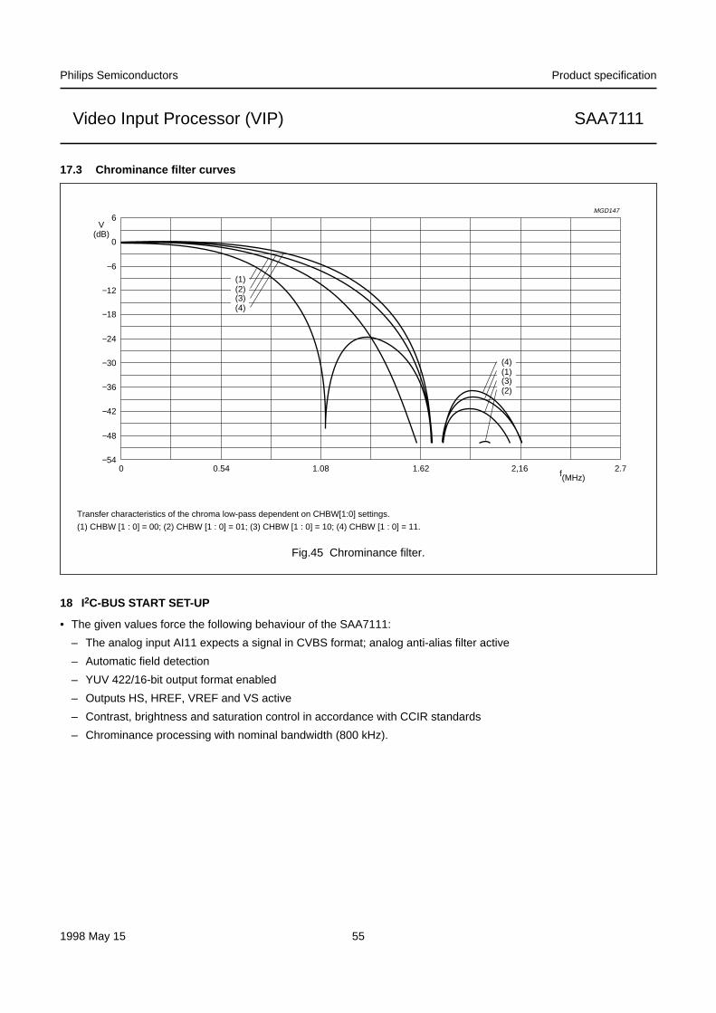
1998 May 15 55
Philips Semiconductors Product specification
Video Input Processor (VIP) SAA7111
17.3 Chrominance filter curves
18 I2C-BUS START SET-UP
• The given values force the following behaviour of the SAA7111:
– The analog input AI11 expects a signal in CVBS format; analog anti-alias filter active
– Automatic field detection
– YUV 422/16-bit output format enabled
– Outputs HS, HREF, VREF and VS active
– Contrast, brightness and saturation control in accordance with CCIR standards
– Chrominance processing with nominal bandwidth (800 kHz).
Fig.45 Chrominance filter.
Transfer characteristics of the chroma low-pass dependent on CHBW[1:0] settings.
(1) CHBW [1 : 0] = 00; (2) CHBW [1 : 0] = 01; (3) CHBW [1 : 0] = 10; (4) CHBW [1 : 0] = 11.
handbook, full pagewidth
2.7
6
0
−6
−12
−18
−24
−30
−36
−42
−48
−540 0.54 1.08 1.62 2,16
MGD147
f(MHz)
V(dB)
(1)(2)(3)(4)
(4)(1)(3)(2)

1998 May 15 56
Philips Semiconductors Product specification
Video Input Processor (VIP) SAA7111
Table 36 I2C-bus start set-up values
Notes
1. All X values must be set to LOW.
2. The I2C-bus subaddress 00 has to be initialized with 0 prior to reading.
SUB(HEX)
FUNCTION NAME(1)VALUES (BIN) (HEX)
7 6 5 4 3 2 1 0 START
00 chip version ID0(7 : 0); note 2 0 0 0 0 0 0 0 0 00
01 reserved 0 0 0 0 0 0 0 0 00
02 analog input control 1 FUSE(1 : 0), GUDL(2 : 0) andMODE(2 : 0)
1 1 0 0 0 0 0 0 C0
03 analog input control 2 X, HLNRS, VBSL, WPOFF, HOLDG,GAFIX, GAI2 and GAI18
0 0 1 0 0 0 1 1 33
04 analog input control 3 GAI(17 : 10) 0 0 0 0 0 0 0 0 00
05 analog input control 4 GAI(27 : 20) 0 0 0 0 0 0 0 0 00
06 horizontal sync start HSB(7 : 0) 1 1 1 0 1 0 1 1 EB
07 horizontal sync stop HSS(7 : 0) 1 1 1 0 0 0 0 0 E0
08 sync control AUFD, FSEL, EXFIL, X, VTRC and HPLLand VNOI(1 : 0)
1 0 0 0 1 0 0 0 88
09 luminance control BYPS, PREF, BPSS(1 : 0), VBLB,UPTCV and APER(1 : 0)
0 0 0 0 0 0 0 1 01
0A luminance brightness BRIG(7 : 0) 1 0 0 0 0 0 0 0 80
0B luminance contrast CONT(7 : 0) 0 1 0 0 0 1 1 1 47
0C chrominance saturation SATN(7 : 0) 0 1 0 0 0 0 0 0 40
0D chroma hue control HUEC(7 : 0) 0 0 0 0 0 0 0 0 00
0E chrominance control CDTO, CM99, CSTD(1 : 0), DCCF, FCTCand CHBW(1 : 0)
0 0 0 0 0 0 0 1 01
0F reserved 0 0 0 0 0 0 0 0 00
10 format/delay control OFTS(1 : 0), HDEL(1 : 0), VRLN andYDEL(2 : 0)
0 1 0 0 0 0 0 0 40
11 output control 1 GPSW, X, FECO, COMPO, OEYC,OEHV, VIPB and COLO
0 0 0 1 1 1 0 0 1C
12 output control 2 RTSE(1 : 0), X, CBR, RGB888, DIT andAOSL(1 : 0)
0 0 0 0 0 0 0 1 03
13 to19
reserved 0 0 0 0 0 0 0 0 00
1A text slicer status 0, 0, 0, 0, F2VAL, F2RDY, F1VAL andF1RDY
read only register
1B decoded bytes of thetext slicer
P1 and BYTE1(6 : 0)
1C P2 and BYTE2(6 : 0)
1D to1E
reserved 0 0 0 0 0 0 0 0 00
1F status byte STTC, HLCK, FIDT, GLIMT, GLIMB,WIPA and SLTCA and CODE
read only register

1998 May 15 57
Philips Semiconductors Product specification
Video Input Processor (VIP) SAA7111
19 PACKAGE OUTLINES
REFERENCESOUTLINEVERSION
EUROPEANPROJECTION ISSUE DATE
IEC JEDEC EIAJ
Note
1. Plastic or metal protrusions of 0.01 inches maximum per side are not included.
SOT188-2
4460
681
9
10 26
43
27
61
detail X
(A )3
bp
w M
A1A
A4
Lp
b1
βk1
k
Xy
e
E
B
DH
EH
v M B
D
ZD
A
ZE
e
v M A
pin 1 index
112E10 MO-047AC
0 5 10 mm
scale
92-11-1795-03-11
PLCC68: plastic leaded chip carrier; 68 leads SOT188-2
UNIT AA
min. max. max. max. max.1 A4 bp E(1) (1) (1)
e HEZywv β
mm 4.574.19 0.51 3.30
0.530.33
0.0210.013
1.27 0.51 2.16
45o0.18 0.100.18
DIMENSIONS (millimetre dimensions are derived from the original inch dimensions)
D(1)
24.3324.13
HD
25.2725.02
EZ
2.16
Db1
0.810.66
k
1.221.07
k1
0.1800.165 0.020 0.13
A3
0.25
0.01 0.05 0.020 0.0850.007 0.0040.007
Lp
1.441.02
0.0570.040
0.9580.950
24.3324.13
0.9580.950
0.9950.985
25.2725.02
0.9950.985
eEeD
23.6222.61
0.9300.890
23.6222.61
0.9300.890 0.085
0.0320.026
0.0480.042
Ee
inches
De

1998 May 15 58
Philips Semiconductors Product specification
Video Input Processor (VIP) SAA7111
UNIT A1 A2 A3 bp c E(1) e HE L Lp Zywv θ
REFERENCESOUTLINEVERSION
EUROPEANPROJECTION ISSUE DATE
IEC JEDEC EIAJ
mm 0.250.10
2.752.55 0.25
0.450.30
0.230.13
14.113.9 0.8
17.4516.95
1.20.8
70
o
o0.16 0.100.161.60
DIMENSIONS (mm are the original dimensions)
Note
1. Plastic or metal protrusions of 0.25 mm maximum per side are not included.
1.030.73
SOT393-1 MS-02296-05-2197-08-04
D(1) (1)(1)
14.113.9
HD
17.4516.95
EZ
1.20.8
D
e
θ
E A1A
Lp
detail X
L
(A )3
B
16
y
c
EHA2
D
ZD
A
ZE
e
v M A
1
64
49
48 33
32
17
X
bp
DH
bp
v M B
w M
w M
0 5 10 mm
scale
pin 1 index
QFP64: plastic quad flat package; 64 leads (lead length 1.6 mm); body 14 x 14 x 2.7 mm SOT393-1
Amax.
3.00
1998 May 15 59
Philips Semiconductors Product specification
Video Input Processor (VIP) SAA7111
20 SOLDERING
20.1 Introduction
There is no soldering method that is ideal for all ICpackages. Wave soldering is often preferred whenthrough-hole and surface mounted components are mixedon one printed-circuit board. However, wave soldering isnot always suitable for surface mounted ICs, or forprinted-circuits with high population densities. In thesesituations reflow soldering is often used.
This text gives a very brief insight to a complex technology.A more in-depth account of soldering ICs can be found inour “IC Package Databook” (order code 9398 652 90011).
20.2 Reflow soldering
Reflow soldering techniques are suitable for all PLCC andQFP packages.
The choice of heating method may be influenced by largerPLCC or QFP packages (44 leads, or more). If infrared orvapour phase heating is used and the large packages arenot absolutely dry (less than 0.1% moisture content byweight), vaporization of the small amount of moisture inthem can cause cracking of the plastic body. For moreinformation, refer to the Drypack chapter in our “QualityReference Handbook” (order code 9397 750 00192).
Reflow soldering requires solder paste (a suspension offine solder particles, flux and binding agent) to be appliedto the printed-circuit board by screen printing, stencilling orpressure-syringe dispensing before package placement.
Several methods exist for reflowing; for example,infrared/convection heating in a conveyor type oven.Throughput times (preheating, soldering and cooling) varybetween 50 and 300 seconds depending on heatingmethod. Typical reflow peak temperatures range from215 to 250 °C.
20.3 Wave soldering
20.3.1 PLCC
Wave soldering techniques can be used for all PLCCpackages if the following conditions are observed:
• A double-wave (a turbulent wave with high upwardpressure followed by a smooth laminar wave) solderingtechnique should be used.
• The longitudinal axis of the package footprint must beparallel to the solder flow.
• The package footprint must incorporate solder thieves atthe downstream corners.
20.3.2 QFP
Wave soldering is not recommended for QFP packages.This is because of the likelihood of solder bridging due toclosely-spaced leads and the possibility of incompletesolder penetration in multi-lead devices.
If wave soldering cannot be avoided, for QFPpackages with a pitch (e) larger than 0.5 mm, thefollowing conditions must be observed:
• A double-wave (a turbulent wave with high upwardpressure followed by a smooth laminar wave)soldering technique should be used.
• The footprint must be at an angle of 45 ° to the boarddirection and must incorporate solder thievesdownstream and at the side corners.
20.3.3 METHOD (PLCC AND QFP)
During placement and before soldering, the package mustbe fixed with a droplet of adhesive. The adhesive can beapplied by screen printing, pin transfer or syringedispensing. The package can be soldered after theadhesive is cured.
Maximum permissible solder temperature is 260 °C, andmaximum duration of package immersion in solder is10 seconds, if cooled to less than 150 °C within6 seconds. Typical dwell time is 4 seconds at 250 °C.
A mildly-activated flux will eliminate the need for removalof corrosive residues in most applications.
20.4 Repairing soldered joints
Fix the component by first soldering two diagonally-opposite end leads. Use only a low voltage soldering iron(less than 24 V) applied to the flat part of the lead. Contacttime must be limited to 10 seconds at up to 300 °C. Whenusing a dedicated tool, all other leads can be soldered inone operation within 2 to 5 seconds between270 and 320 °C.
CAUTION
Wave soldering is NOT applicable for all QFPpackages with a pitch (e) equal or less than 0.5 mm.

1998 May 15 60
Philips Semiconductors Product specification
Video Input Processor (VIP) SAA7111
21 DEFINITIONS
22 LIFE SUPPORT APPLICATIONS
These products are not designed for use in life support appliances, devices, or systems where malfunction of theseproducts can reasonably be expected to result in personal injury. Philips customers using or selling these products foruse in such applications do so at their own risk and agree to fully indemnify Philips for any damages resulting from suchimproper use or sale.
23 PURCHASE OF PHILIPS I2C COMPONENTS
Data sheet status
Objective specification This data sheet contains target or goal specifications for product development.
Preliminary specification This data sheet contains preliminary data; supplementary data may be published later.
Product specification This data sheet contains final product specifications.
Limiting values
Limiting values given are in accordance with the Absolute Maximum Rating System (IEC 134). Stress above one ormore of the limiting values may cause permanent damage to the device. These are stress ratings only and operationof the device at these or at any other conditions above those given in the Characteristics sections of the specificationis not implied. Exposure to limiting values for extended periods may affect device reliability.
Application information
Where application information is given, it is advisory and does not form part of the specification.
Purchase of Philips I2C components conveys a license under the Philips’ I2C patent to use thecomponents in the I2C system provided the system conforms to the I2C specification defined byPhilips. This specification can be ordered using the code 9398 393 40011.

1998 May 15 61
Philips Semiconductors Product specification
Video Input Processor (VIP) SAA7111
NOTES

1998 May 15 62
Philips Semiconductors Product specification
Video Input Processor (VIP) SAA7111
NOTES

1998 May 15 63
Philips Semiconductors Product specification
Video Input Processor (VIP) SAA7111
NOTES

Internet: http://www.semiconductors.philips.com
Philips Semiconductors – a worldwide company
© Philips Electronics N.V. 1998 SCA60
All rights are reserved. Reproduction in whole or in part is prohibited without the prior written consent of the copyright owner.
The information presented in this document does not form part of any quotation or contract, is believed to be accurate and reliable and may be changedwithout notice. No liability will be accepted by the publisher for any consequence of its use. Publication thereof does not convey nor imply any licenseunder patent- or other industrial or intellectual property rights.
Middle East: see Italy
Netherlands: Postbus 90050, 5600 PB EINDHOVEN, Bldg. VB,Tel. +31 40 27 82785, Fax. +31 40 27 88399
New Zealand: 2 Wagener Place, C.P.O. Box 1041, AUCKLAND,Tel. +64 9 849 4160, Fax. +64 9 849 7811
Norway: Box 1, Manglerud 0612, OSLO,Tel. +47 22 74 8000, Fax. +47 22 74 8341
Pakistan: see Singapore
Philippines: Philips Semiconductors Philippines Inc.,106 Valero St. Salcedo Village, P.O. Box 2108 MCC, MAKATI,Metro MANILA, Tel. +63 2 816 6380, Fax. +63 2 817 3474
Poland: Ul. Lukiska 10, PL 04-123 WARSZAWA,Tel. +48 22 612 2831, Fax. +48 22 612 2327
Portugal: see Spain
Romania: see Italy
Russia: Philips Russia, Ul. Usatcheva 35A, 119048 MOSCOW,Tel. +7 095 755 6918, Fax. +7 095 755 6919
Singapore: Lorong 1, Toa Payoh, SINGAPORE 319762,Tel. +65 350 2538, Fax. +65 251 6500
Slovakia: see Austria
Slovenia: see Italy
South Africa: S.A. PHILIPS Pty Ltd., 195-215 Main Road Martindale,2092 JOHANNESBURG, P.O. Box 7430 Johannesburg 2000,Tel. +27 11 470 5911, Fax. +27 11 470 5494
South America: Al. Vicente Pinzon, 173, 6th floor,04547-130 SÃO PAULO, SP, Brazil,Tel. +55 11 821 2333, Fax. +55 11 821 2382
Spain: Balmes 22, 08007 BARCELONA,Tel. +34 93 301 6312, Fax. +34 93 301 4107
Sweden: Kottbygatan 7, Akalla, S-16485 STOCKHOLM,Tel. +46 8 5985 2000, Fax. +46 8 5985 2745
Switzerland: Allmendstrasse 140, CH-8027 ZÜRICH,Tel. +41 1 488 2741 Fax. +41 1 488 3263
Taiwan: Philips Semiconductors, 6F, No. 96, Chien Kuo N. Rd., Sec. 1,TAIPEI, Taiwan Tel. +886 2 2134 2865, Fax. +886 2 2134 2874
Thailand: PHILIPS ELECTRONICS (THAILAND) Ltd.,209/2 Sanpavuth-Bangna Road Prakanong, BANGKOK 10260,Tel. +66 2 745 4090, Fax. +66 2 398 0793
Turkey: Talatpasa Cad. No. 5, 80640 GÜLTEPE/ISTANBUL,Tel. +90 212 279 2770, Fax. +90 212 282 6707
Ukraine : PHILIPS UKRAINE, 4 Patrice Lumumba str., Building B, Floor 7,252042 KIEV, Tel. +380 44 264 2776, Fax. +380 44 268 0461
United Kingdom: Philips Semiconductors Ltd., 276 Bath Road, Hayes,MIDDLESEX UB3 5BX, Tel. +44 181 730 5000, Fax. +44 181 754 8421
United States: 811 East Arques Avenue, SUNNYVALE, CA 94088-3409,Tel. +1 800 234 7381
Uruguay: see South America
Vietnam: see Singapore
Yugoslavia: PHILIPS, Trg N. Pasica 5/v, 11000 BEOGRAD,Tel. +381 11 625 344, Fax.+381 11 635 777
For all other countries apply to: Philips Semiconductors,International Marketing & Sales Communications, Building BE-p, P.O. Box 218,5600 MD EINDHOVEN, The Netherlands, Fax. +31 40 27 24825
Argentina: see South America
Australia: 34 Waterloo Road, NORTH RYDE, NSW 2113,Tel. +61 2 9805 4455, Fax. +61 2 9805 4466
Austria: Computerstr. 6, A-1101 WIEN, P.O. Box 213, Tel. +43 160 1010,Fax. +43 160 101 1210
Belarus: Hotel Minsk Business Center, Bld. 3, r. 1211, Volodarski Str. 6,220050 MINSK, Tel. +375 172 200 733, Fax. +375 172 200 773
Belgium: see The Netherlands
Brazil: see South America
Bulgaria: Philips Bulgaria Ltd., Energoproject, 15th floor,51 James Bourchier Blvd., 1407 SOFIA,Tel. +359 2 689 211, Fax. +359 2 689 102
Canada: PHILIPS SEMICONDUCTORS/COMPONENTS,Tel. +1 800 234 7381
China/Hong Kong: 501 Hong Kong Industrial Technology Centre,72 Tat Chee Avenue, Kowloon Tong, HONG KONG,Tel. +852 2319 7888, Fax. +852 2319 7700
Colombia: see South America
Czech Republic: see Austria
Denmark: Prags Boulevard 80, PB 1919, DK-2300 COPENHAGEN S,Tel. +45 32 88 2636, Fax. +45 31 57 0044
Finland: Sinikalliontie 3, FIN-02630 ESPOO,Tel. +358 9 615800, Fax. +358 9 61580920
France: 51 Rue Carnot, BP317, 92156 SURESNES Cedex,Tel. +33 1 40 99 6161, Fax. +33 1 40 99 6427
Germany: Hammerbrookstraße 69, D-20097 HAMBURG,Tel. +49 40 23 53 60, Fax. +49 40 23 536 300
Greece: No. 15, 25th March Street, GR 17778 TAVROS/ATHENS,Tel. +30 1 4894 339/239, Fax. +30 1 4814 240
Hungary: see Austria
India: Philips INDIA Ltd, Band Box Building, 2nd floor,254-D, Dr. Annie Besant Road, Worli, MUMBAI 400 025,Tel. +91 22 493 8541, Fax. +91 22 493 0966
Indonesia: PT Philips Development Corporation, Semiconductors Division,Gedung Philips, Jl. Buncit Raya Kav.99-100, JAKARTA 12510,Tel. +62 21 794 0040 ext. 2501, Fax. +62 21 794 0080
Ireland: Newstead, Clonskeagh, DUBLIN 14,Tel. +353 1 7640 000, Fax. +353 1 7640 200
Israel: RAPAC Electronics, 7 Kehilat Saloniki St, PO Box 18053,TEL AVIV 61180, Tel. +972 3 645 0444, Fax. +972 3 649 1007
Italy: PHILIPS SEMICONDUCTORS, Piazza IV Novembre 3,20124 MILANO, Tel. +39 2 6752 2531, Fax. +39 2 6752 2557
Japan: Philips Bldg 13-37, Kohnan 2-chome, Minato-ku,TOKYO 108-8507, Tel. +81 3 3740 5130, Fax. +81 3 3740 5077
Korea: Philips House, 260-199 Itaewon-dong, Yongsan-ku, SEOUL,Tel. +82 2 709 1412, Fax. +82 2 709 1415
Malaysia: No. 76 Jalan Universiti, 46200 PETALING JAYA, SELANGOR,Tel. +60 3 750 5214, Fax. +60 3 757 4880
Mexico: 5900 Gateway East, Suite 200, EL PASO, TEXAS 79905,Tel. +9-5 800 234 7381
Printed in The Netherlands 655102/1200/03/pp64 Date of release: 1998 May 15 Document order number: 9397 750 03116