video/image processing on fpga · pdf filevideo/image processing on fpga by jin zhao ... 2.6...
TRANSCRIPT

Video/Image Processing on FPGA
by
Jin Zhao
A Thesis
Submitted to the Faculty
of the
WORCESTER POLYTECHNIC INSTITUTE
In partial fulfillment of the requirements for the
Degree of Master of Science
in
Electrical and Computer Engineering
by
April 2015
APPROVED:
Professor Xinming Huang, Major Thesis Advisor
Professor Lifeng Lai
Professor Emmanuel O. Agu

Abstract
Video/Image processing is a fundamental issue in computer science. It is widely
used for a broad range of applications, such as weather prediction, computerized
tomography (CT), artificial intelligence (AI), and etc. Video-based advanced driver
assistance system (ADAS) attracts great attention in recent years, which aims at
helping drivers to become more concentrated when driving and giving proper warn-
ings if any danger is insight. Typical ADAS includes lane departure warning, traffic
sign detection, pedestrian detection, and etc. Both basic and advanced video/image
processing technologies are deployed in video-based driver assistance system. The
key requirements of driver assistance system are rapid processing time and low power
consumption. We consider Field Programmable Gate Array (FPGA) as the most
appropriate embedded platform for ADAS. Owing to the parallel architecture, an
FPGA is able to perform high-speed video processing such that it could issue warn-
ings timely and provide drivers longer time to response. Besides, the cost and power
consumption of modern FPGAs, particular small size FPGAs, are considerably ef-
ficient. Compared to the CPU implementation, the FPGA video/image processing
achieves about tens of times speedup for video-based driver assistance system and
other applications.

Acknowledgements
I would like to sincerely express my gratitude to my advisor, Professor Xinming
Huang. He offered me the opportunity to study and develop myself in Worcester
Polytechnic Institute, guided me in the research projects and mentored me in my
life.
Thanks to Sichao Zhu for his creative and helpful work in the traffic sign detection
project. Thanks to Bingqian Xie for her ideas and experiments in the lane departure
warning system project. Thanks to Boyang Li for helping me learn how to build
basic video/image processing block using Mathworks tools.
Thanks to The Mathworks. Inc for their generously supporting our research,
financially and professionally.
Thanks to all my lovely friends and my family for their help in the past years.
They always encourage me and give me confidence to overcome all the problems.
i

Contents
1 Introduction 1
2 Basic Video/Image Processing 3
2.1 Digital Image/Video Fundamentals . . . . . . . . . . . . . . . . . . . 3
2.2 Mathworks HDL Coder Introduction . . . . . . . . . . . . . . . . . . 5
2.3 Color Correction . . . . . . . . . . . . . . . . . . . . . . . . . . . . . 7
2.3.1 Introduction . . . . . . . . . . . . . . . . . . . . . . . . . . . . 7
2.3.2 Simulink Implementation . . . . . . . . . . . . . . . . . . . . . 8
2.3.3 FPGA Implementation . . . . . . . . . . . . . . . . . . . . . . 11
2.4 RGB2YUV . . . . . . . . . . . . . . . . . . . . . . . . . . . . . . . . 15
2.4.1 Introduction . . . . . . . . . . . . . . . . . . . . . . . . . . . . 15
2.4.2 Simulink Implementation . . . . . . . . . . . . . . . . . . . . . 17
2.4.3 FPGA Implementation . . . . . . . . . . . . . . . . . . . . . . 18
2.5 Gamma Correction . . . . . . . . . . . . . . . . . . . . . . . . . . . . 19
2.5.1 Introduction . . . . . . . . . . . . . . . . . . . . . . . . . . . . 19
2.5.2 Simulink Implementation . . . . . . . . . . . . . . . . . . . . . 21
2.5.3 FPGA Implementation . . . . . . . . . . . . . . . . . . . . . . 22
2.6 2D FIR Filter . . . . . . . . . . . . . . . . . . . . . . . . . . . . . . . 23
2.6.1 Introduction . . . . . . . . . . . . . . . . . . . . . . . . . . . . 23
ii

2.6.2 Simulink Implementation . . . . . . . . . . . . . . . . . . . . . 26
2.6.3 FPGA Implementation . . . . . . . . . . . . . . . . . . . . . . 28
2.7 Median Filter . . . . . . . . . . . . . . . . . . . . . . . . . . . . . . . 29
2.7.1 Introduction . . . . . . . . . . . . . . . . . . . . . . . . . . . . 29
2.7.2 Simulink Implementation . . . . . . . . . . . . . . . . . . . . . 30
2.7.3 FPGA Implementation . . . . . . . . . . . . . . . . . . . . . . 33
2.8 Sobel Filter . . . . . . . . . . . . . . . . . . . . . . . . . . . . . . . . 34
2.8.1 Introduction . . . . . . . . . . . . . . . . . . . . . . . . . . . . 34
2.8.2 Simulink Implementation . . . . . . . . . . . . . . . . . . . . . 35
2.8.3 FPGA Implementation . . . . . . . . . . . . . . . . . . . . . . 36
2.9 Grayscale to Binary Image . . . . . . . . . . . . . . . . . . . . . . . . 37
2.9.1 Introduction . . . . . . . . . . . . . . . . . . . . . . . . . . . . 37
2.9.2 Simulink Implementation . . . . . . . . . . . . . . . . . . . . . 39
2.9.3 FPGA Implementation . . . . . . . . . . . . . . . . . . . . . . 41
2.10 Binary/Morphological Image Processing . . . . . . . . . . . . . . . . 41
2.10.1 Introduction . . . . . . . . . . . . . . . . . . . . . . . . . . . . 41
2.10.2 Simulink Implementation . . . . . . . . . . . . . . . . . . . . . 43
2.10.3 FPGA Implementation . . . . . . . . . . . . . . . . . . . . . . 44
2.11 Summary . . . . . . . . . . . . . . . . . . . . . . . . . . . . . . . . . 45
3 Advanced Video/Image Processing 46
3.1 Lane Departure warning system . . . . . . . . . . . . . . . . . . . . . 46
3.1.1 Introduction . . . . . . . . . . . . . . . . . . . . . . . . . . . . 46
3.1.2 Approaches to Lane Departure Warning . . . . . . . . . . . . 47
3.1.3 Hardware Implementation . . . . . . . . . . . . . . . . . . . . 52
3.1.4 Experimental Results . . . . . . . . . . . . . . . . . . . . . . . 56
3.2 Traffic Sign Detection System Using SURF . . . . . . . . . . . . . . . 58
iii

3.2.1 Introduction . . . . . . . . . . . . . . . . . . . . . . . . . . . . 58
3.2.2 SURF Algorithm . . . . . . . . . . . . . . . . . . . . . . . . . 59
3.2.3 FPGA Implementation of SURF . . . . . . . . . . . . . . . . . 61
3.2.3.1 Overall system architecture . . . . . . . . . . . . . . 62
3.2.3.2 Integral image generation . . . . . . . . . . . . . . . 63
3.2.3.3 Interest points detector . . . . . . . . . . . . . . . . 64
3.2.3.4 Memory management unit . . . . . . . . . . . . . . . 67
3.2.3.5 Interest point descriptor . . . . . . . . . . . . . . . . 68
3.2.3.6 Descriptor Comparator . . . . . . . . . . . . . . . . 69
3.2.4 Results . . . . . . . . . . . . . . . . . . . . . . . . . . . . . . . 70
3.3 Traffic Sign Detection System Using SURF and FREAK . . . . . . . 71
3.3.1 FREAK Descriptor . . . . . . . . . . . . . . . . . . . . . . . . 72
3.3.2 Hardware Implementation . . . . . . . . . . . . . . . . . . . . 73
3.3.2.1 Overall System Architecture . . . . . . . . . . . . . . 73
3.3.2.2 Integral Image Generator and Interest Point Detector 74
3.3.2.3 Memory Management Unit . . . . . . . . . . . . . . 75
3.3.2.4 FREAK Descriptor . . . . . . . . . . . . . . . . . . . 76
3.3.2.5 Descriptor Matching Module . . . . . . . . . . . . . 77
3.3.3 Results . . . . . . . . . . . . . . . . . . . . . . . . . . . . . . . 78
3.4 Summary . . . . . . . . . . . . . . . . . . . . . . . . . . . . . . . . . 79
4 Conclusions 80
iv

List of Figures
1.1 Xilinx KC705 development kit . . . . . . . . . . . . . . . . . . . . . 2
2.1 Video stream timing signals . . . . . . . . . . . . . . . . . . . . . . . 5
2.2 HDL supported Simulink library . . . . . . . . . . . . . . . . . . . . . 6
2.3 Illustration of color correction . . . . . . . . . . . . . . . . . . . . . . 8
2.4 Flow chart of color correction system in Simulink . . . . . . . . . . . 9
2.5 Flow chart of video format conversion block . . . . . . . . . . . . . . 10
2.6 Flow chart of serialize block . . . . . . . . . . . . . . . . . . . . . . . 10
2.7 Flow chart of deserialize block . . . . . . . . . . . . . . . . . . . . . . 10
2.8 Implementation of color correction block in Simulink . . . . . . . . . 11
2.9 Example of color correction in Simulink . . . . . . . . . . . . . . . . . 12
2.10 HDL coder workflow advisor (1) . . . . . . . . . . . . . . . . . . . . . 13
2.11 HDL coder workflow advisor (2) . . . . . . . . . . . . . . . . . . . . . 13
2.12 HDL coder workflow advisor (3) . . . . . . . . . . . . . . . . . . . . . 14
2.13 HDL coder workflow advisor (4) . . . . . . . . . . . . . . . . . . . . . 14
2.14 HDL coder workflow advisor (5) . . . . . . . . . . . . . . . . . . . . . 15
2.15 Example of color correction on hardware . . . . . . . . . . . . . . . . 15
2.16 Illustration of RGB to YUV conversion . . . . . . . . . . . . . . . . . 16
2.17 Flow chart of RGB2YUV Simulink system . . . . . . . . . . . . . . . 17
2.18 Implementation of RGB2YUV block in Simulink . . . . . . . . . . . . 18
v

2.19 Example of RGB2YUV in Simulink . . . . . . . . . . . . . . . . . . . 19
2.20 Example of RGB2YUV on hardware . . . . . . . . . . . . . . . . . . 20
2.21 Illustration of gamma correction . . . . . . . . . . . . . . . . . . . . . 21
2.22 Flow chart of gamma correction system in Simulink . . . . . . . . . . 22
2.23 Parameter settings for 1-D Lookup Table . . . . . . . . . . . . . . . 22
2.24 Example of gamma correction in Simulink . . . . . . . . . . . . . . . 23
2.25 Example of gamma correction on hardware . . . . . . . . . . . . . . . 24
2.26 Illustration of 2D FIR filter . . . . . . . . . . . . . . . . . . . . . . . 25
2.27 Flow chart of 2D FIR filter system in Simulink . . . . . . . . . . . . . 26
2.28 Flow chart of 2D FIR filter block in Simulink . . . . . . . . . . . . . 26
2.29 Flow chart of Sobel Kernel block . . . . . . . . . . . . . . . . . . . . 27
2.30 Architecture of kernel mult block . . . . . . . . . . . . . . . . . . . . 27
2.31 Example of 2D FIR filter in Simulink . . . . . . . . . . . . . . . . . . 28
2.32 Example of 2D FIR filter on hardware . . . . . . . . . . . . . . . . . 28
2.33 Illustration of median filter . . . . . . . . . . . . . . . . . . . . . . . . 30
2.34 Flow chart of median filter block in Simulink . . . . . . . . . . . . . . 31
2.35 Flow chart of the median Simulink block . . . . . . . . . . . . . . . . 31
2.36 Architecture of the compare block in Simulink . . . . . . . . . . . . . 32
2.37 Implementation of basic compare block in Simulink . . . . . . . . . . 32
2.38 Example of median filter in Simulink . . . . . . . . . . . . . . . . . . 33
2.39 Example of median filter on hardware . . . . . . . . . . . . . . . . . . 34
2.40 Illustration of Sobel filter . . . . . . . . . . . . . . . . . . . . . . . . . 35
2.41 Flow chart of Sobel filter block in Simulink . . . . . . . . . . . . . . . 35
2.42 Flow chart of the Sobel kernel block in Simulink . . . . . . . . . . . . 36
2.43 Flow chart of the x/y directional block in Sobel filter system . . . . . 37
2.44 Example of Sobel filter in Simulink . . . . . . . . . . . . . . . . . . . 38
vi
2.45 Example of Sobel filter on hardware . . . . . . . . . . . . . . . . . . . 38
2.46 Illustration of grayscale to binary image conversion . . . . . . . . . . 39
2.47 Flow chart of the proposed grayscale to binary image conversion systems 40
2.48 Implementation of the gray2bin block in Simulink . . . . . . . . . . . 40
2.49 Example of grayscale to binary image conversion in Simulink . . . . . 40
2.50 Example of grayscale to binary image conversion on hardware . . . . 41
2.51 Illustration of morphological image processing . . . . . . . . . . . . . 43
2.52 Flow chart of the proposed image dilation block . . . . . . . . . . . . 44
2.53 Detail of the bit operation block . . . . . . . . . . . . . . . . . . . . . 44
2.54 Example of image dilation in Simulink . . . . . . . . . . . . . . . . . 45
2.55 Example of image dilation on hardware . . . . . . . . . . . . . . . . . 45
3.1 Flow chart of the proposed LDW and FCW systems . . . . . . . . . . 48
3.2 Illustration of Sobel filter and Otsu’s threshold binarization. (a) is
the original image captured from camera. (b) and (c) are ROI after
Sobel filtering and binarization, respectively . . . . . . . . . . . . . . 50
3.3 Hough transform from 2D space to Hough space . . . . . . . . . . . . 51
3.4 Sobel filter architecture . . . . . . . . . . . . . . . . . . . . . . . . . . 53
3.5 Datapath for Otsu’s threshold calculation . . . . . . . . . . . . . . . . 53
3.6 Hough transform architecture . . . . . . . . . . . . . . . . . . . . . . 54
3.7 Flow chart of front vehicle detection . . . . . . . . . . . . . . . . . . . 55
3.8 Results of our LDW and FCW systems . . . . . . . . . . . . . . . . . 57
3.9 Overall system block diagram . . . . . . . . . . . . . . . . . . . . . . 62
3.10 Integral image generation block diagram . . . . . . . . . . . . . . . . 63
3.11 Build Hessian Response block diagram . . . . . . . . . . . . . . . . . 65
3.12 Is Extreme block diagram . . . . . . . . . . . . . . . . . . . . . . . . 66
3.13 Interest point descriptor block diagram . . . . . . . . . . . . . . . . . 68
vii

3.14 Traffic sign detection system . . . . . . . . . . . . . . . . . . . . . . . 71
3.15 Illustration of the FREAK sampling pattern . . . . . . . . . . . . . . 72
3.16 FPGA design system block diagram . . . . . . . . . . . . . . . . . . . 74
3.17 Integral image address generator. . . . . . . . . . . . . . . . . . . . . 75
3.18 Normalized intensity calculation. . . . . . . . . . . . . . . . . . . . . 76
3.19 Descriptor matching flow chart . . . . . . . . . . . . . . . . . . . . . 77
3.20 A matching example of STOP sign detection . . . . . . . . . . . . . . 79
viii

List of Tables
3.1 Device utilization summary . . . . . . . . . . . . . . . . . . . . . . . 56
3.2 Device utilization summary . . . . . . . . . . . . . . . . . . . . . . . 71
3.3 Device utilization summary . . . . . . . . . . . . . . . . . . . . . . . 78
ix
Chapter 1
Introduction
Video/image processing is any form of signal processing for which the input is an
video/image, such as a video stream or photograph. Video/image needs to be pro-
cessed for better display, storage and other special purposes. For example, medical
scientists enhance x-ray images and suppress accompanying noises for doctors to
make precise diagnosis. Video/image processing also builds solid groundwork for
computer vision, video/image compression, machine learning and etc.
In this thesis we focus on real-time video/image processing for advanced driver
assistance system (ADAS). Each year millions of traffic accidents occurred around
the world cause loss of lives and property. Improving road safety through advanced
computing and sensor technologies has drawn lots of interests from researchers and
corporations. Video-based driver-assistance system is becoming an indispensable
part of smart vehicles. It monitors and interprets the surrounding traffic situation,
which greatly improves driving safety. ADAS includes, but is not limited to, lane
departure warning, traffic sign detection, pedestrian detection, etc. Unlike general
video/image processing on computer, driver assistance system naturally requires
rapid video/image processing as well as low power consumption. Alternative solution
1

should be considered for ADAS rather than general purpose CPU.
Field Programmable Gate Array (FPGA) is an reconfigurable integrated circuit.
Its parallel computational architecture an convenient access to local memories make
it the most appropriate platform for driver assistance system. An FPGA is able to
perform real-time video processing such that it could issue corresponding warnings
to the drivers timely. Besides, the cost and power consumption of modern FPGAs
are relatively low, compared to CPU and GPU. In this thesis work, we employ Xilinx
KC705 FPGA development kit in figure 1.1 as the hardware platform.
Figure 1.1: Xilinx KC705 development kit
This thesis is organized as follows. Chapter 2 introduces the basic video/image
processing blocks and their implementation on FPGA. Chapter 3 presents advanced
video/image processing algorithms for driver assistance system and their FPGA
implementation. Chapter 4 concludes our achievements and possible improvement
in the work of future.
2

Chapter 2
Basic Video/Image Processing
This chapter starts with introduction of digital video/image, then presents basic
video/image processing blocks. Basic video/image processing is not only broadly
used in simple video systems, but could be fundamental and indispensable compo-
nent in complex video projects. In the thesis, we cover the following video pro-
cessing functions: color correction, RGB to YUV conversion, gamma correction,
median filter, 2D FIR filter, Sobel filter, grayscale to binary conversion and mor-
phological image processing. For every functional block, this thesis introduces basic
idea, builds the blocks using Mathworks Simulink and HDL Coder toolbox, and
implements hardware block on FPGA.
2.1 Digital Image/Video Fundamentals
A digital image could be defined as a two-dimensional function f (x, y), where the
x and y are spatial coordinates, and the amplitude of f (x, y) at any location of an
image is called the intensity of the image at that point as (2.1).
3

f =
f (1, 1) f (1, 2) · · · f (1, n)
f (2, 1) f (2, 2) · · · f (2, n)
......
...
f (m, 1) f (m, 2) · · · f (m,n)
(2.1)
Color image includes color information for each pixel. It could be seen as a
combination of individual images of different color channels. The mainly used color
system in computer displays are RGB (Red, Green, Blue) space. Other color image
representation systems are HSI (Hue, Saturation, Intensity) and YCbCr or YUV.
Grayscale image refers to monochrome image. The only color of each pixel
is shade of gray. In fact, a gray color is one in which the red, green and blue
components all have equal intensity in RGB space. Hence, it is only necessary to
specify a single intensity value for each pixel, as opposed to represent each pixel
with three intensities in full color images.
For each color channel of RGB image and grayscale image pixel, the intensity is
within a given range between a minimum and maximum value. Often, every pixel
intensity is stored using an 8-bit integer giving 256 possible different grades from 0
and 255. The black is 0 and the white is 255, respectively.
Binary image, or black and white image, is a kind of digital image that has only
two possible intensity value for every pixel, 1 as white and 0 for black. The object
is labeled with foreground color while the rest of the image is with the background
color.
Video stream is a series of successive images. Every video frame consists of
active pixels and blanking as figure 2.1. At the end of each line, there is a portion
of waveform called horizontal blanking interval. The horizontal sync signal ’hsync’
indicates start of the next line. Starting from the top, all the active lines on the
4

Figure 2.1: Video stream timing signals
display area are scanned in this way. Once the entire active video frame is scanned,
there is another portion of waveform called vertical blanking interval. The vertical
sync signal ’vsync’ indicates start of the new video frame. The time slot of blanking
could be used to process video stream, which we can see in the following chapters.
2.2 Mathworks HDL Coder Introduction
Matlab/Simulink is a high-level language for scientific and technical computing in-
troduced by Mathworks, Inc. Matlab/Simulink takes matrix as basic data element
and makes tremendous matrix operation optimization. Therefore, Matlab is perfect
for video/image processing since video/image is naturally matrix.
HDL coder is a Matlab toolbox product. It generates portable, synthesizable
Verilog and VHDL code from Mathworks Matlab, Simulink and Stateflow charts.
The generated HDL code can be used for FPGA programming or ASIC (Application
Specific Integrated Circuit) prototyping and design. HDL Coder provides a workflow
advisor that automates the programming of Xilinx and Altera FPGAs. You can
5
control HDL architecture and implementation, highlight critical paths, and generate
hardware resource utilization estimates.
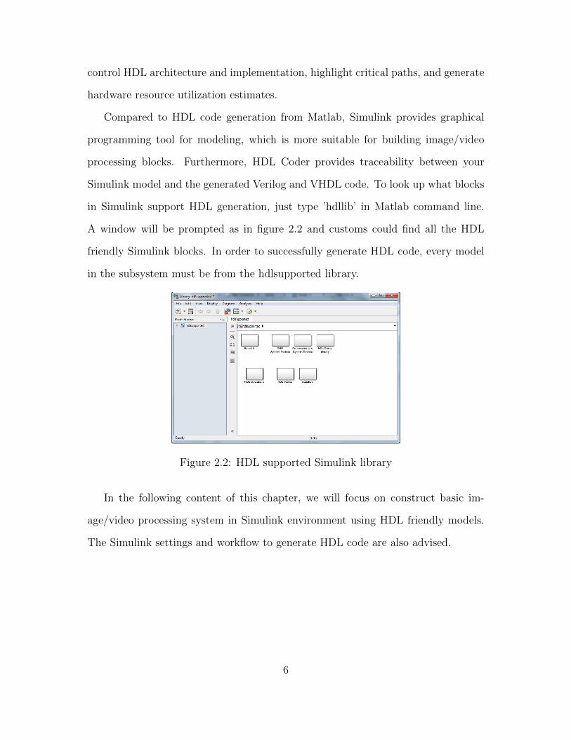
Compared to HDL code generation from Matlab, Simulink provides graphical
programming tool for modeling, which is more suitable for building image/video
processing blocks. Furthermore, HDL Coder provides traceability between your
Simulink model and the generated Verilog and VHDL code. To look up what blocks
in Simulink support HDL generation, just type ’hdllib’ in Matlab command line.
A window will be prompted as in figure 2.2 and customs could find all the HDL
friendly Simulink blocks. In order to successfully generate HDL code, every model
in the subsystem must be from the hdlsupported library.
Figure 2.2: HDL supported Simulink library
In the following content of this chapter, we will focus on construct basic im-
age/video processing system in Simulink environment using HDL friendly models.
The Simulink settings and workflow to generate HDL code are also advised.
6

2.3 Color Correction
2.3.1 Introduction
Color inaccuracies exist commonly during image/video acquisition. An error white
balance setting or inappropriate color temperature will produce color errors. In
most digital still and video imaging systems, color correction is to alter the overall
color of the light. In RGB color space, color image is stored in m×n× 3 arrays and
each pixel could be represented as 3D vector [R,G,B]′. The color channel correction
matrix M is applied to the input images in order to correct color inaccuracies. The
correction could be expressed by an multiplication as the following equality in (2.2):
Rout
Gout
Bout
=
M11 M12 M13
M21 M22 M23
M31 M32 M33
×Rin
Gin
Bin
(2.2)
or be unfolded in 3 items as
Rout = M11 ×Rin +M12 ×Gin +M13 ×Bin (2.3)
Gout = M21 ×Rin +M22 ×Gin +M23 ×Bin (2.4)
Bout = M31 ×Rin +M32 ×Gin +M33 ×Bin (2.5)
There are several solution to estimate the color correction matrix. For example,
Least-squares solution could make the matrix more robust and less influenced by
outliers. In the typical workflow, a test chart with known and randomly distributed
color patches was captured by a digital camera with “auto” white balance. Com-
7

parison of means of the red, green and blue color components in the color patches,
original versus captured, reveal the presence of non-linearity. The non-linearity
could be described using a 3 × 3 matrix N . In order to accurately display the real
color, we employ inverse matrix M = N−1 to offset non-linearity of video camera.
For example, In fig. 2.3, (a) is the generated original color patches. (b) is image
(a) with color inaccuracies. All the color patches seem containing more red compo-
nents. The color drifting could be modeled with matrix N and we could correct the
incorrect color patches with M = N−1 and get recovered image (c).
(a) (b) (c)
Figure 2.3: Illustration of color correction
2.3.2 Simulink Implementation
Simulink, provided by Mathworks, is a graphical block diagram environment for
modeling, simulating and analyzing multi-domain dynamic systems. Its interface
is a block diagramming tool and a set of block libraries. It supports simulation,
verification and automatic code generation.
Simulink is easy-to-use and efficient way to modeling functional algorithms. The
8
method is pretty straightforward: 1) create a new Simulink model. 2) type ’simulink’
in Matlab command line to view all available Simulink library blocks. 3) type ’hdl-
lib’ in Matlab command line and open all Simulink block that support HDL code
generation. 4) use these HDL friendly block to build up functional blocks hierar-
chically. You can do so by copying blocks from Simulink library and hdlsupported
library to your Simulink model, then simply draw connection lines to link blocks.
Simulink simulates a dynamic system by computing the states of all blocks at
a series of time steps over a chosen time span, using information defined by the
model. The Simulink library of solvers is divided into two major types: fixed-step
and variable-step. They can further be divided within each of these categories
as: discrete or continuous, explicit or implicit, one-step or multi-step, and single-
order or variable-order. For all the image processing demos in this thesis, variable
step discrete solver is selected. You can go to Simulink → Model Configuration
Parameters and select correct solver in the Solver tab of prompted window.
We will elaborate the basic steps and other algorithms in this chapter follow
the same guideline. It is important to point out that we just need to translate key
processing algorithms to HDL and so other parts of Simulink model, such as source,
sink, pre-processing and etc, are not necessarily from hdlsupported library.
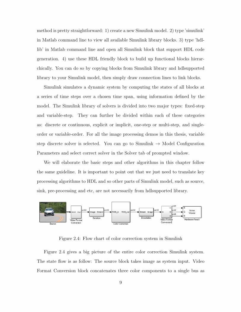
Figure 2.4: Flow chart of color correction system in Simulink
Figure 2.4 gives a big picture of the entire color correction Simulink system.
The state flow is as follow: The source block takes image as system input. Video
Format Conversion block concatenates three color components to a single bus as
9

in Figure 2.5. Serialize block converts image matrix to pixel-by-pixel stream. Fig.
2.6 illustrates the inner structure of Serialize block. Color correction block is the
key componentamong those modules. This block must be purely set up with funda-
mental blocks from hdlsupported library and hence could be translated to Verilog
and VHDL using HDL coder work flow. The subsequent Serialize block as fig. 2.7,
inverse of Serialize, convert serial pixel stream back to image matrix. The final block
- Video Viewer displays filtering result in Simulink.
Figure 2.5: Flow chart of video format conversion block
Figure 2.6: Flow chart of serialize block
Figure 2.7: Flow chart of deserialize block
Fig. 2.8 illustrates color correction block Simulink implementation. The input
bus signal is separated to three color components RGB. The gain blocks implement
multiplication. The sum blocks sum up previous multiplication products. Matrix
10

multiplication is implemented using these gain and sum blocks. Finally the corrected
color components are concatenated again to a bus signal. The delay blocks inserted
in between will be transferred to registers in hardware, which add more clock cycles
to leverage higher clock frequency.
Figure 2.8: Implementation of color correction block in Simulink
Fig 2.9 gives the simulation result in Simulink environment. Image (a) is the
RGB image with color inaccuracy and image (b) is the corrected image using color
correction Simulink system.
2.3.3 FPGA Implementation
After successfully making a functional Simulink project based on HDL friendly basic
blocks, we could simply generate HDL code from it using Mathworks HDL coder
toolbox.
11

(a) (b)
Figure 2.9: Example of color correction in Simulink
In the first step, right click the HDL friendly subsystem and select HDL Code
→ HDL Workflow Advisor. In the Set Target → Set Target Device and Synthesis
Tool step, for Synthesis tool, select Xilinx ISE and click Run This Task as in fig.
2.10.
In the second step as in fig. 2.12, right-click Prepare Model For HDL Code Gen-
eration and select Run All. The HDL Workflow Advisor checks the model for code
generation compatibility. You may encounter some incorrect model configuration
settings problems for HDL code generation as figure 2.11. To fix the problem, click
the Modify All button, or click the hyperlink to launch the Configuration Parameter
dialog and manually apply the recommended settings.
In the HDL Code Generation → Set Code Generation Options → Set Basic
Options step, select the following options, then click Apply: For Language, select
Verilog, Enable Generate traceability report, Enable Generate resource utilization
report. For the options available in the Optimization and Coding style tabs, you
can use these options to modify the implementation and format of the generated
code. This step is showed in fig. 2.13.
12
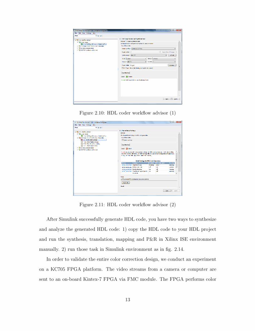
Figure 2.10: HDL coder workflow advisor (1)
Figure 2.11: HDL coder workflow advisor (2)
After Simulink successfully generate HDL code, you have two ways to synthesize
and analyze the generated HDL code: 1) copy the HDL code to your HDL project
and run the synthesis, translation, mapping and P&R in Xilinx ISE environment
manually. 2) run those task in Simulink environment as in fig. 2.14.
In order to validate the entire color correction design, we conduct an experiment
on a KC705 FPGA platform. The video streams from a camera or computer are
sent to an on-board Kintex-7 FPGA via FMC module. The FPGA performs color
13

Figure 2.12: HDL coder workflow advisor (3)
Figure 2.13: HDL coder workflow advisor (4)
correction on every video frame and exports the results to a monitor for display. We
delay the video pixel timing signals vsync, hsync and de accordingly to match pixel
delay cycles in Simulink.
The reported maximum frequency is 228.94 MHz. The resources utilization of
the color correction system on FPGA is as follows : 102 slice registers and 246 slice
LUTs. Fig. 2.15 illustrates the result of our color correction system on hardware.
Image (a) is an video image with color inaccuracy and image (b) is the corrected
14

Figure 2.14: HDL coder workflow advisor (5)
(a) (b)
Figure 2.15: Example of color correction on hardware
image with accurate color.
2.4 RGB2YUV
2.4.1 Introduction
Color image processing is a logical extension to the processing of grayscale images.
The main difference is that each pixel consists of a vector of components rather
15

than a scalar. Usually, a pixel from an image has three components: red, green and
blue. These are defined by the human visual system. Color is typically represented
by a three dimensional vector and user can define how many bits each component
have. Besides using RGB to represent the color of an image, there are different
ways to represent an image to make subsequent analysis or processing easier, such
as CMYK (subtractive color model, mainly used in color printing) and YUV (used
for video/image compression and television system). Here Y stands for luminance
signal, which is the combination of RGB components, with the color provided by
two color difference signals U and V.
Because many video/image processing is performed in YUV space or simply in
grayscale, so RGB to YUV conversion is very desirable in many video system. We
can use simple functions to show convert these components like:
Y = 0.299R + 0.587G+ 0.114B (2.6)
U = 0.492(B − Y ) (2.7)
V = 0.877(R− Y ) (2.8)
(a) (b) (c) (d)
Figure 2.16: Illustration of RGB to YUV conversion
16

Fig 2.16 illustrates the result of convert color image in RGB domain to image
with YUV components. Image (a) is the color image with RGB representation and
(b) (c) (d) is YUV components of the image, respectively.
2.4.2 Simulink Implementation
Figure 2.17: Flow chart of RGB2YUV Simulink system
Figure 2.17 gives an overview of the entire RGB2YUV Simulink system. The
other blocks are exactly identical with those in color correction model except the
RGB2YUV kernel block. The kernel block detail is shown in fig. 2.18. The input
bus signal is represented in Xilinx video data format, which is 32’hFFRRBBGG. So
we first separate the bus signal to three color components RGB. Red component is
bit 23 to 16; Green is bit 7 to 0; Blue is bit 15 to 8. The gain blocks implement
multiplication. The sum blocks calculate add and subtract result, which are defined
in block parameter. Matrix multiplication is implemented using these gain and
sum blocks. Finally the corrected color components are concatenated again to a
bus signal. The delay blocks inserted in between will be transferred to registers in
hardware, which break down the critical path to achieve higher clock frequency.
17

Figure 2.18: Implementation of RGB2YUV block in Simulink
Fig 2.19 gives the simulation result in Simulink environment. Image (a) is the
color image with RGB representation and (b) (c) (d) is YUV components of the
image, respectively.
2.4.3 FPGA Implementation
We validate the entire RGB2YUV design on a KC705 FPGA platform using gener-
ated HDL code. The reported maximum frequency is 159.69 MHz. The resources
utilization of the RGB to YUV system on FPGA is as follows: 106 slice registers
and 286 slice LUTs. Fig. 2.20 illustrates the result of our RGB to YUV system on
hardware. Image (a) is the color image with RGB representation and (b) (c) (d) is
YUV components of the image, respectively. To display Y(U/V) component in gray
scale, we assign the value of signal component to all RGB channels.
18

(a) (b)
(c) (d)
Figure 2.19: Example of RGB2YUV in Simulink
2.5 Gamma Correction
2.5.1 Introduction
Gamma correction is a nonlinear operation used to adjust pixel luminance in video
or still image systems. Image seems bleach out or too dark when it is not properly
corrected. Gamma correction controls the overall brightness of an image, crucial for
displaying an image accurately on a computer screen.
Gamma correction could be defined by the following power-law expression:
Vout = K × V rin (2.9)
where K is a constant coefficient and Vin/Vout is non-negative real values. In the
19

(a) (b)
(c) (d)
Figure 2.20: Example of RGB2YUV on hardware
common case of K = 1, the inputs and outputs are normalized in the range of [0, 1].
For 8-bit grayscale image, the input/output range is between [0, 255]. For the case
that gamma value r < 1, it is called an encoding gamma; conversely a gamma value
r > 1 is called a decoding gamma.
Gamma correction is necessary for image display due to nonlinear property of
computer monitor. Almost all computer monitors have an intensity to voltage re-
sponse curve which is roughly r = 2.2 power function. When computer monitor is
sent a certain pixel of intensity x, it will actually display a pixel with intensity x2.2.
This means that the intensity value displayed is less than what it is expected to be.
For instance, 0.52.2 = 0.22.
To correct this annoying bug, the input image intensity to the monitor must be
gamma corrected. Since the relationship between the voltage sent to monitor and
intensity displayed could be depicted by gamma coefficient r and monitor manufac-
tures provide the number, we could correct the signal before it reaches the monitor
20
(a) (b)
(c) (d)
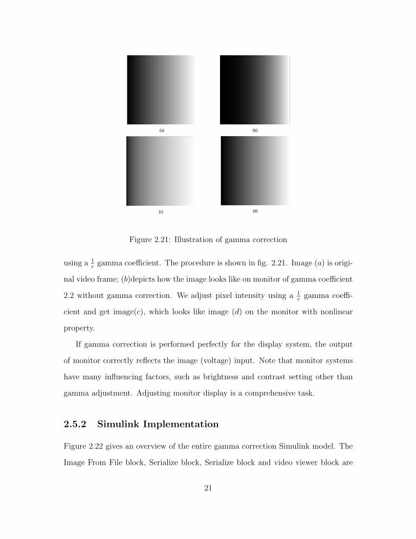
Figure 2.21: Illustration of gamma correction
using a 1r
gamma coefficient. The procedure is shown in fig. 2.21. Image (a) is origi-
nal video frame; (b)depicts how the image looks like on monitor of gamma coefficient
2.2 without gamma correction. We adjust pixel intensity using a 1r
gamma coeffi-
cient and get image(c), which looks like image (d) on the monitor with nonlinear
property.
If gamma correction is performed perfectly for the display system, the output
of monitor correctly reflects the image (voltage) input. Note that monitor systems
have many influencing factors, such as brightness and contrast setting other than
gamma adjustment. Adjusting monitor display is a comprehensive task.
2.5.2 Simulink Implementation
Figure 2.22 gives an overview of the entire gamma correction Simulink model. The
Image From File block, Serialize block, Serialize block and video viewer block are
21
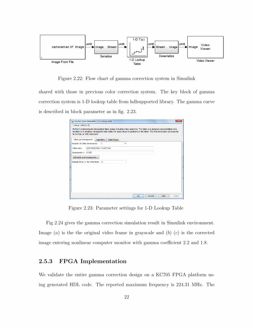
Figure 2.22: Flow chart of gamma correction system in Simulink
shared with those in previous color correction system. The key block of gamma
correction system is 1-D lookup table from hdlsupported library. The gamma curve
is described in block parameter as in fig. 2.23.
Figure 2.23: Parameter settings for 1-D Lookup Table
Fig 2.24 gives the gamma correction simulation result in Simulink environment.
Image (a) is the the original video frame in grayscale and (b) (c) is the corrected
image entering nonlinear computer monitor with gamma coefficient 2.2 and 1.8.
2.5.3 FPGA Implementation
We validate the entire gamma correction design on a KC705 FPGA platform us-
ing generated HDL code. The reported maximum frequency is 224.31 MHz. The
22

(a) (b) (c)
Figure 2.24: Example of gamma correction in Simulink
resources utilization of the gamma correction system on FPGA is as follows: 50
slices, 17 slice flip flops and 95 four input LUTs. Fig. 2.25 illustrates the result of
our gamma correction system on hardware. We apply the same gamma correction
block on all RGB color channels. Image (a) is the original color image with RGB
representation. Image (b) and (c) are the result of gamma correction system of co-
efficients 2.2 and 1.8. Image (d) is what the color image looks like on a real monitor
with nonlinear property.
2.6 2D FIR Filter
2.6.1 Introduction
The 2D FIR filter is a basic filter for image processing. The output signals of a
2D FIR filter can be computed using the input samples and previously computed
output samples as well as filter kernel. For a causal discrete-time FIR filter of order
N of 1 dimension, each value of the output sequence is a weighted sum of the most
recent input values, as shown in equation (2.10):
23

(a) (b)
(d)(c)
Figure 2.25: Example of gamma correction on hardware
y[n] = b0x[n] + b1x[n− 1] + b2x[n− 2] + · · ·+ bNx[n−N ] (2.10)
where x[n] is the input signal and the y[n] is the output signal. N is the filter
order, an Nth order filter has (N+1) terms on the right hand side. bi is the value of
the impulse response at the i-th instant for 0 ≤ i ≤ N of an Nth order FIR filter.
For 2-D FIR filter, the output signals rely on both previous pixels of current line
and pixels of upper lines. Upon the 2D filter kernel, the 2D FIR filter could be
either high-pass filter or low-pass filter. Equation (2.11) and (2.12) gives example
of typical high pass filter kernel and low pass filter kernel.
24
HighPass = [
0 −1 0
−1 4 −1
0 −1 0
] (2.11)
LowPass = [
1/16 1/8 1/16
1/8 1/4 1/8
1/16 1/8 1/16
] (2.12)
(a) (b)
(c) (d)
Figure 2.26: Illustration of 2D FIR filter
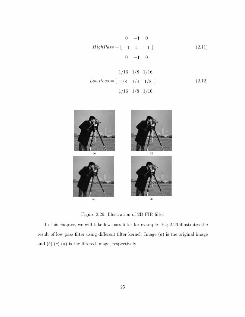
In this chapter, we will take low pass filter for example. Fig 2.26 illustrates the
result of low pass filter using different filter kernel. Image (a) is the original image
and (b) (c) (d) is the filtered image, respectively.
25

Figure 2.27: Flow chart of 2D FIR filter system in Simulink
2.6.2 Simulink Implementation
Figure 2.27 gives an overview of the entire 2D FIR filter Simulink system. The
architecture is also shared with following 2D filters in this chapter. The filtering
block is the only difference. Other blocks are the very same ones.
Figure 2.28: Flow chart of 2D FIR filter block in Simulink
Sobel filter block is implemented as fig. 2.28. We design a Sobel kernel block
to calculate the filter response of input image, then calculate the response absolute
value and convert it to uint8 data type for further display.
Fig. 2.29 is the architecture of Sobel kernel block. The 2D FIR algorithm
maintains three line buffers. Each iteration the input pixel is pushed into the current
line buffer that is being written to. The control logic rotates between these three
buffers when it reaches the column boundary. Each buffer is followed by a shift
register and data at the current column index is pushed into the shift register. At
each iteration a 3x3 kernel of pixels are formed from the pixel input, shift registers
26

Figure 2.29: Flow chart of Sobel Kernel block
and line buffer outputs. The kernel are multiplied by a 3x3 filter coefficient mask
and the sum of the result values is computed as the pixel output as in figure 2.30.
Figure 2.30: Architecture of kernel mult block
Fig 2.31 gives the low pass 2D FIR filter result in Simulink environment. Image
(a) is the the original video frame in grayscale and (b) is smoothed image output
using low pass filter in equation (2.12).
27

(a) (b)
Figure 2.31: Example of 2D FIR filter in Simulink
2.6.3 FPGA Implementation
(a) (b) (c)
Figure 2.32: Example of 2D FIR filter on hardware
We validate the entire 2D FIR filter design on a KC705 FPGA platform using
generated HDL code. The reported maximum frequency is 324.45 MHz. The re-
sources utilization of the 2D FIR filter system on FPGA is as follows: 71 slices, 120
flip flops, 88 four input LUTs and 1 FIFO16/RAM16. Fig. 2.32 illustrates the 2D
FIR filter system on hardware. Image (a) is the color image in grayscale and (b) (c)
is blurred image using different kinds of low pass filter kernels.
28

2.7 Median Filter
2.7.1 Introduction
Median filter is a nonlinear digital filtering technique, usually used for removing the
noise on an image. It is a more robust method than the traditional linear filtering
in some circumstances. The noise reduction is an important pre-processing step to
improve the results of the later process. The main idea of median filter is that using
a sliding window scan the whole image and replaces the center value in the window
with the median of all the pixel values in the window. The input image for median
filter is the grayscale image and the window is replied to each pixel of it. Usually,
we choose the window size as 3 by 3. Here we give an example of how the median
filter work in one window. For example, we have a 3 × 3 pixel window from an
image. The pixel values in the image window are 122, 116, 141, 119, 130, 125, 122,
120, 117. We can calculate what is the median value from the central one and all
the neighborhood values. The median value is 120. So the next step is to replace
the central value with the median value 120.
Compared to basic median filter, adaptive median filter may be more pratical.
In adaptive median filter, we just do the central value - median value swap when
the central value is black (0) or white (255) pixel. Otherwise, the system will keep
the original central pixel intensity.
Fig 2.33 illustrates the result of median filter using different sizes of filter kernel.
Image (a) is the original image; image (b) is image (a) with thin salt and pepper
noise; image (c) is the result of 3×3 median filter applied on image (b); image (d) is
image (a) with thick salt and pepper noise; image (e) is the result of 3× 3 median
filter applied on image (d); image (f) is the result of 5 × 5 median filter applied
on image (d). Comparing those images, we can find that the median filter blurs
29

(a) (b) (c)
(d) (e) (f)
Figure 2.33: Illustration of median filter
input image. With larger median filter mask, we filter out more noise, but lose more
information as well.
2.7.2 Simulink Implementation
The architecture of median filter Simulink system is the same with 2D FIR filter
model in fig. 2.27. The median filter is depicted in fig. 2.34. The median algorithm,
like 2D FIR filter, also maintains three line buffers. Each iteration the input pixel
is pushed into the current line buffer that is being written to. The control logic
rotates between these three buffers when it reaches the column boundary. Each
buffer is followed by a shift register and data at the current column index is pushed
into the shift register. At each iteration a 3x3 kernel of pixels are formed from the
pixel input, shift registers and line buffer outputs. Then the median block decide
the median output. Note that our adaptive median filter is design to filter out salt
30

Figure 2.34: Flow chart of median filter block in Simulink
and pepper noise. It should be modified in order to handle other kinds of error. It
first chooses the median intensity of input 9 input pixels in compare block in fig.
2.35, then compares the current pixel intensity with 0 and 255. If the pixel is salt
or pepper, the switch block chooses median value as output; otherwise it just passes
through current pixel intensity.
Figure 2.35: Flow chart of the median Simulink block
Fig. 2.36 shows the architecture of compare block. It is built with 19 basic
31

Figure 2.36: Architecture of the compare block in Simulink
Figure 2.37: Implementation of basic compare block in Simulink
compare blocks as in fig. 2.37. The basic compare blocks, taking 2 data input,
employ 2 relational operators and 2 switches to get the larger one and smaller one.
With such design, we get the median pixel value of 9 input pixels.
Fig 2.38 gives the median filter result in Simulink environment. Image (a) and
(c) is the the original video frame in different density of salt and pepper noise.
Image(b) and (d) is the recovered images using our 3× 3 median filter block.
32

(a) (b)
(c) (d)
Figure 2.38: Example of median filter in Simulink
2.7.3 FPGA Implementation
We validate the entire adaptive median filter design on the KC705 FPGA platform
using generated HDL code. The reported maximum frequency is 374.92 MHz. The
resources utilization of the median filter system on FPGA is as follows: 81 slices, 365
slice LUTs and 1 Block RAM/FIFO. Fig. 2.39 illustrates the median filter system
on hardware. Image (a) and (b) are the original grayscale image and image with
salt and pepper noise. Image (c) is recovered image using generated RTL median
filter.
33

(a) (b) (c)
Figure 2.39: Example of median filter on hardware
2.8 Sobel Filter
2.8.1 Introduction
The Sobel operator performs a 2-D spatial gradient measurement on an image and
so emphasizes regions of high frequency that correspond to edges. Typically it is
used to find the approximate absolute gradient magnitude at each point in an input
grayscale image. Here we also need a window to do the scanning work and here
we still choose 3 by 3 as the size of the window, then we apply two kernels on the
sliding window separately and independently. The x directional kernel is shown as
the following equation:
Gx =
0.125 0 −0.125
0.25 0 −0.25
0.125 0 −0.125
and y directional kernel is similar. By summing up the x and y directional kernel
response, we get the final Sobel filter response.
Fig 2.40 illustrates the result of Sobel filter. Image (a) is the original image;
34

(a) (b)
Figure 2.40: Illustration of Sobel filter
output image (b) is highlighted result using Sobel filter;
2.8.2 Simulink Implementation
Figure 2.41: Flow chart of Sobel filter block in Simulink
The architecture of Sobel filter Simulink system is the same with 2D FIR filter
system in fig. 2.27. The Sobel filter block filter is depicted in fig. 2.41. It first
calculates Sobel filter response in x and y direction in Sobel kernel block, then sum
their absolute values to get the final Sobel filter response and quantize the response
to Uint8 type for following display.
35
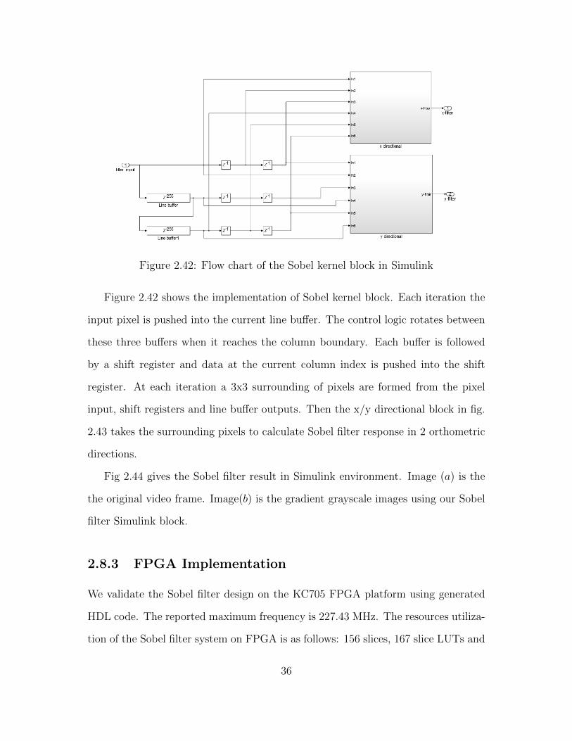
Figure 2.42: Flow chart of the Sobel kernel block in Simulink
Figure 2.42 shows the implementation of Sobel kernel block. Each iteration the
input pixel is pushed into the current line buffer. The control logic rotates between
these three buffers when it reaches the column boundary. Each buffer is followed
by a shift register and data at the current column index is pushed into the shift
register. At each iteration a 3x3 surrounding of pixels are formed from the pixel
input, shift registers and line buffer outputs. Then the x/y directional block in fig.
2.43 takes the surrounding pixels to calculate Sobel filter response in 2 orthometric
directions.
Fig 2.44 gives the Sobel filter result in Simulink environment. Image (a) is the
the original video frame. Image(b) is the gradient grayscale images using our Sobel
filter Simulink block.
2.8.3 FPGA Implementation
We validate the Sobel filter design on the KC705 FPGA platform using generated
HDL code. The reported maximum frequency is 227.43 MHz. The resources utiliza-
tion of the Sobel filter system on FPGA is as follows: 156 slices, 167 slice LUTs and
36

Figure 2.43: Flow chart of the x/y directional block in Sobel filter system
1 Block RAM/FIFO. Fig. 2.45 illustrates the Sobel filter system on hardware. Im-
age (a) is the original grayscale image and (b) is sharpened image with Sobel filter,
which highlights all the edges containing most critical information of the image.
2.9 Grayscale to Binary Image
2.9.1 Introduction
Converting grayscale image to binary image is often used in order to find Region
of Interest - a portion of image that is of interest for further processing because
binary image processing reduces the computational complexity. For example, Hough
transform is widely used to detect straight lines, circle and other specific curve in
an image and it takes only binary image input.
Grayscale image to binary image conversion always follows a high pass filter,
such as Sobel filter, to highlight the key information of an image, which is always
boundary of object. Subsequently, the key step of grayscale to binary conversion is
to set up an threshold. Each pixel of gradient image generated by highpass filter is
37

(a) (b)
Figure 2.44: Example of Sobel filter in Simulink
(a) (b)
Figure 2.45: Example of Sobel filter on hardware
compared to the chosen threshold. If the pixel intensity is larger than the threshold,
it is set to 1 in the binary image. Otherwise, it is set to 0.
We could imagine an appropriate threshold determine the quality of converted
binary image. Unfortunately, there isn’t a single threshold working for every image.
A threshold good for bright scene could never work for dark scene, and vice versa.
In section 3.1.2, we introduce an adaptive thresholding method to convert grayscale
image to binary image. Here, we will focus on fixed threshold method.
Fig 2.46 illustrates the result of grayscale to binary image conversion using dif-
38
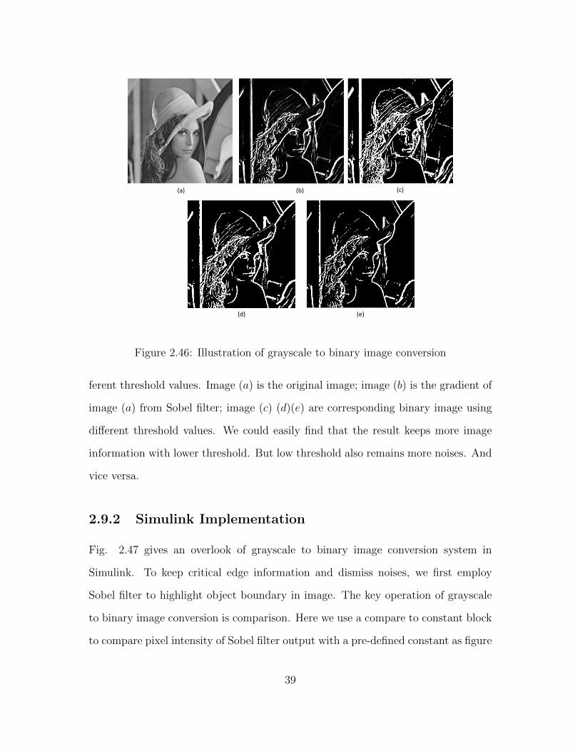
(b)
(d)
(a) (c)
(e)
Figure 2.46: Illustration of grayscale to binary image conversion
ferent threshold values. Image (a) is the original image; image (b) is the gradient of
image (a) from Sobel filter; image (c) (d)(e) are corresponding binary image using
different threshold values. We could easily find that the result keeps more image
information with lower threshold. But low threshold also remains more noises. And
vice versa.
2.9.2 Simulink Implementation
Fig. 2.47 gives an overlook of grayscale to binary image conversion system in
Simulink. To keep critical edge information and dismiss noises, we first employ
Sobel filter to highlight object boundary in image. The key operation of grayscale
to binary image conversion is comparison. Here we use a compare to constant block
to compare pixel intensity of Sobel filter output with a pre-defined constant as figure
39

Figure 2.47: Flow chart of the proposed grayscale to binary image conversion sys-tems
2.48. This will produce an output a binary image of 1 (white) and 0 (black).
Figure 2.48: Implementation of the gray2bin block in Simulink
(a) (b) (c)
Figure 2.49: Example of grayscale to binary image conversion in Simulink
Fig 2.49 gives the grayscale to binary image conversion result in Simulink envi-
ronment. Image (a) is the original grayscale image; image (b) is high-passed image
using Sobel filter; image (c) is converted binary representation of image content.
40

(a) (b)
Figure 2.50: Example of grayscale to binary image conversion on hardware
2.9.3 FPGA Implementation
We validate the grayscale to binary conversion design on the KC705 FPGA platform
using generated HDL code. The reported maximum frequency is 426.13 MHz. The
resources utilization of the grayscale to binary system on FPGA is as follows: 9
slices registers and 2 slice LUTs. Fig. 2.50 illustrates the grayscale to binary system
on hardware. Image (a) is the original grayscale image; image (b) is corresponding
binary image, which keeps the main information of original grayscale image.
2.10 Binary/Morphological Image Processing
2.10.1 Introduction
Morphological image processing is a collection of non-linear operations related to
the shape or morphology of features in an image. Morphological technique typically
probes a binary image with a small shape or template known as structuring ele-
ment consisting of only 0’s and 1’s. The structuring element could be any size and
positioned at any possible locations in the image.
A lot of morphological image processing is conducted in 3 × 3 neighborhood.
41
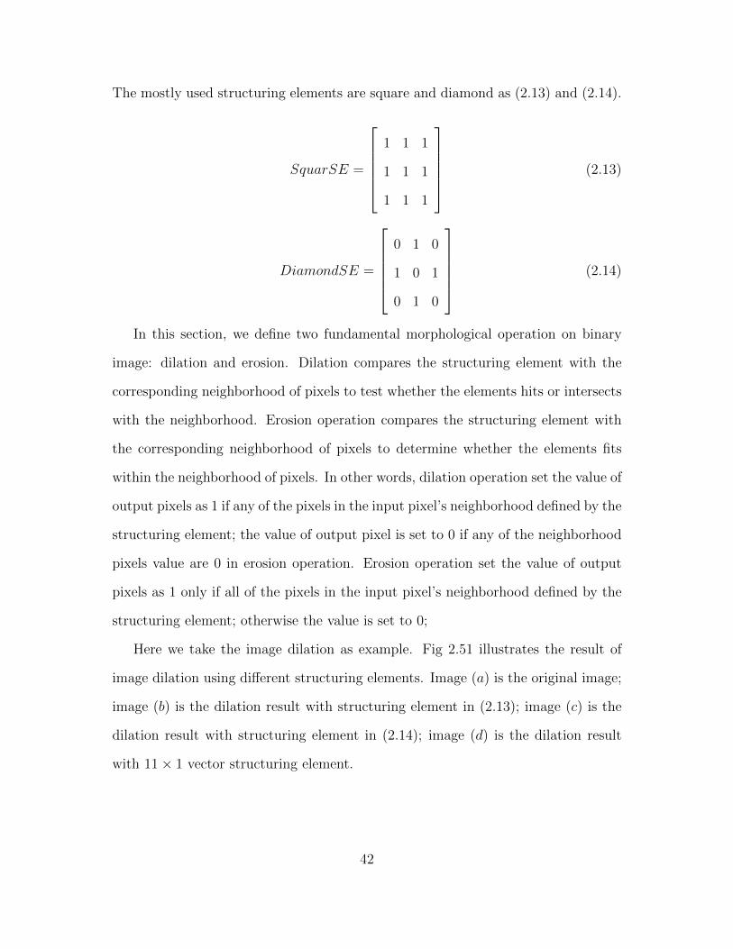
The mostly used structuring elements are square and diamond as (2.13) and (2.14).
SquarSE =
1 1 1
1 1 1
1 1 1
(2.13)
DiamondSE =
0 1 0
1 0 1
0 1 0
(2.14)
In this section, we define two fundamental morphological operation on binary
image: dilation and erosion. Dilation compares the structuring element with the
corresponding neighborhood of pixels to test whether the elements hits or intersects
with the neighborhood. Erosion operation compares the structuring element with
the corresponding neighborhood of pixels to determine whether the elements fits
within the neighborhood of pixels. In other words, dilation operation set the value of
output pixels as 1 if any of the pixels in the input pixel’s neighborhood defined by the
structuring element; the value of output pixel is set to 0 if any of the neighborhood
pixels value are 0 in erosion operation. Erosion operation set the value of output
pixels as 1 only if all of the pixels in the input pixel’s neighborhood defined by the
structuring element; otherwise the value is set to 0;
Here we take the image dilation as example. Fig 2.51 illustrates the result of
image dilation using different structuring elements. Image (a) is the original image;
image (b) is the dilation result with structuring element in (2.13); image (c) is the
dilation result with structuring element in (2.14); image (d) is the dilation result
with 11× 1 vector structuring element.
42

(a) (b)
(c) (d)
Figure 2.51: Illustration of morphological image processing
2.10.2 Simulink Implementation
Fig. 2.52 gives an overlook of image dilation block in Simulink. The delay blocks
collect current pixel surroundings (according to structuring element) for bit opera-
tion blocks to perform subsequent calculation. The key operation of binary image
morphology is bit operation. For image erosion application, bits AND operation is
preformed; for image dilation application, we need to perform bits OR operation.
For example, a 5-input OR operation is applied to perform image dilation in fig.
2.53.
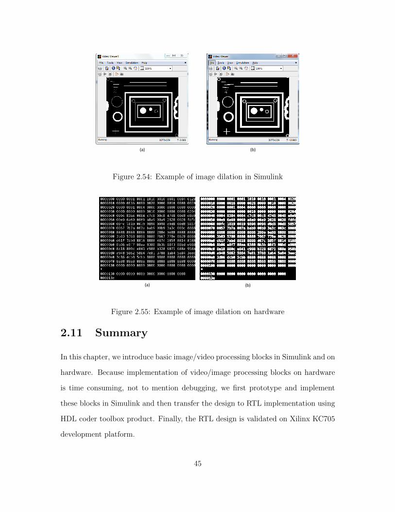
Fig 2.54 gives the image dilation result in Simulink environment. Image (a) is
the original binary image; image (b) is dilated image output using 3 × 3 square
structuring element.
43

Figure 2.52: Flow chart of the proposed image dilation block
Figure 2.53: Detail of the bit operation block
2.10.3 FPGA Implementation
We validate the image dilation design on the KC705 FPGA platform using gener-
ated HDL code. The reported maximum frequency is 359.02 MHz. The resources
utilization of the image dilation system on FPGA is as follows: 28 slice registers, 32
slice LUTs and 1 Block RAM/FIFO. Fig. 2.55 illustrates the image dilation system
on hardware. Image (a) is the original binary image and (b) is dilated image using
generated image dilation HDL code.
44
(a) (b)
Figure 2.54: Example of image dilation in Simulink
(a) (b)
Figure 2.55: Example of image dilation on hardware
2.11 Summary
In this chapter, we introduce basic image/video processing blocks in Simulink and on
hardware. Because implementation of video/image processing blocks on hardware
is time consuming, not to mention debugging, we first prototype and implement
these blocks in Simulink and then transfer the design to RTL implementation using
HDL coder toolbox product. Finally, the RTL design is validated on Xilinx KC705
development platform.
45

Chapter 3
Advanced Video/Image Processing
3.1 Lane Departure warning system
3.1.1 Introduction
Each year millions of traffic accidents occurred around the world cause loss of lives
and properties. Improving road safety through advanced computing and sensor
technologies has drawn lots of interests from the auto industry. Advanced Driver
assistance system (ADAS) thus gains great popularity, which helps drivers to prop-
erly handle different driving condition and giving warnings if any danger is insight.
Typical driver assistance system includes, but is not limited to, lane departure
warning, traffic sign detection [1], obstacle detection [2], pedestrian detection [3],
etc. Many accidents were caused by careless or drowsy drivers, who failed to notice
that their cars were drifting to neighboring lanes or were too close to the car in the
front. Therefore, lane departure warning (LDW) system and front collision warning
(FCW) system are designed to prevent this type of accidents.
Different methods have been proposed for lane keeping and front vehicle detec-
tion. Marzotto et al. [4] proposed a RANSAC-like approach to minimize computa-
46

tional and memory cost. Risack et al. [5] used a lane state model for lane detection
and evaluated lane keeping performance as a parameter called time to line cross-
ing (TLC). McCall et al. [6] proposed a ’video-based lane estimation and tracking’
(VioLET) system which uses steerable filters to detect the lane marks. Others used
Hough transform for feature based lane detection. Wang et al. [7] combined Hough
transform and Otsu’s threshold method together to improve the performance of lane
detection and implemented it on a Kintex FPGA platform. Lee et al. [8] removed
redundant operations and proposed an optimized Hough transform design which
uses fewer logic gates and less number of cycles when implemented on an FPGA
board. Lin et al. [9] integrated lane departure warning system and front collision
warning system on a DSP board.
The key requirements of a driver assistance system are rapid processing time and
low power consumption. We consider FPGA as the most appropriate platform for
such a task. Owing to the parallel architecture, an FPGA can perform high-speed
video processing such that it can issue warnings timely and provide drivers more
time to response. Besides, the cost and power consumption of modern FPGAs,
particularly small size FPGAs, are considerably efficient.
In this contribution, we present a monocular vision lane departure warning and
front collision warning system jointly implemented on a single FPGA device. Our
experimental results demonstrate that the FPGA-based design is fully functional
and it achieves the real-time performance of 160 frame-per-second (fps) for high
resolution 720P video.
3.1.2 Approaches to Lane Departure Warning
The proposed LDW and FCW system takes video input from a single camera
mounted on a car windshield. Fig. 3.1 shows the flow chart of the proposed LDW
47

Sobel Filter
Otsu ThresholdBinarization
Hough Transform
Lane Detection
Departure
Lane Departure Warning
Gradient Image
Binary Image
Peak
T
Shadow Detection
Distance Calculation
LUT
Collision
Front Collision Warning
With Velocity
T
Image Dilation
Grayscale Image
Figure 3.1: Flow chart of the proposed LDW and FCW systems
and FCW systems. The first step is to apply a Sobel filter on the gray scale image
frame to sharpen the edges after an RGB to gray scale conversion. This operation
helps highlight the lane marks and front vehicle boundary while eliminating dirty
noise on the road. The operator of Sobel filter is
G = G2x +G2
y (3.1)
where the Gx is Sobel kernel in x - direction as in (3.2) and similarly Gy in y-
direction.
Gx =
0.125 0 −0.125
0.25 0 −0.25
0.125 0 −0.125
(3.2)
Next, an important task is to convert the gray scale video frame to a “perfect”
binary image which is used by both LDW and FCW systems. A “perfect” binary
48

image means high signal-to-noise ratio, preserving desired information while aban-
doning useless data to produce more accurate results and to ease computational
burden. For LDW and FCW systems, the desired information is lane marks of the
road and vehicles in the front. Therefore, we cut off the top part of every image
and crop the area of interest to the bottom 320 rows of a 720P picture. All subse-
quent calculations are conducted on this region of interest (ROI). When converting
from gray scale to binary image, a fixed threshold is often not effective since the
illumination variance has apparent influence on the binarization. Instead, we choose
Otsu’s threshold, a dynamic and adaptive method, to obtain binary image that is
insensitive to background changes. The first step of Otsu’s method is to calculate
probability distribution of each gray level as in (3.3).
pi = ni/N (3.3)
where pi and ni are probability and pixel number of gray level i. N is the total
pixel number of all possible levels (from 0 to 255 for gray scale). The second is to
step through all possible level t to calculate ω∗(t) and µ∗(t) as in (3.4) and (3.5).
ω∗ (t) =t∑
i=0
pi (3.4)
µ∗ (t) =t∑
i=0
ipi (3.5)
The final step is to calculate between-class variance (σ∗B(t))2 as in (3.6).
(σ∗B (t))2 =[µ∗Tω
∗ (t)− µ∗ (t)]2
ω∗ (t)× [1− ω∗ (t)](3.6)
where µ∗T is µ∗(255) in this case. For easy implementation on an FPGA, (3.6) is
49

re-written as (3.7)
σ2B (t) =
[µT/N × ω (t)− µ (t)]2
ω (t)× [N − ω (t)](3.7)
where ω (t) = ω∗ (t)×N and µ (t) = µ∗ (t)×N . Otsu’s method selects level t∗ as
binarization threshold, which has largest σ2B(t∗). Fig. 3.2 illustrates effects of Sobel
filter and Otsu’s threshold binarization.
(a)
(b)
(c)
Figure 3.2: Illustration of Sobel filter and Otsu’s threshold binarization. (a) is theoriginal image captured from camera. (b) and (c) are ROI after Sobel filtering andbinarization, respectively
Image dilation is a basic morphology operation. It usually uses a structuring
element for probing and expanding shapes in a binary image. In this design, we
apply image dilation to smooth toothed edges introduced by Sobel filter, which can
50

Figure 3.3: Hough transform from 2D space to Hough space
assist the subsequent operations to perform better.
Furthermore, Hough transform (HT) is widely used as a proficient way of finding
lines and curves in binary image. Since most lines on a road are almost straight
in pictures, we mainly discuss the way of finding straight lines in binary image
using Hough transform. Every point (x,y) in 2D space can be represented in polar
coordinate system as
ρ = xcos (θ) + ysin (θ) (3.8)
Fig. 3.3 illustrates 2D space to Hough space mapping. If point A and B are
on the same straight line, there exists a pair of ρ and θ that satisfy both equation,
which means two curves in polar coordinate have an intersection point. As more
points on the same line are added to the polar system, there should be one shared
intersection point between these curves. In Hough transform algorithm, it keeps
track of all intersection points between curves and the intersections with big voting
imply that there is a straight line in 2D space.
By analyzing Hough transform for lane detection, we optimize the transform
during the following two steps: 1) dividing the image into a left part and a right
part, perform HT with positive θ for the left part and negative θ for the right part
due to the slope nature of the lanes; 2) further shrink the range of θ by ignoring
51

those lines that are almost horizontal with θ near ±90. Empirically, the range of
θ is set to [1, 65] for the left part and [−65,−1] for the right part. We choose the
most voted (ρ, θ) pairs of left part and right part as detected left lane and right
lane, respectively. To avoid occasional errors on a single frame, the detected lanes
are compared with results from preceded 4 frames. If they are outliers, the system
takes weighted average of results of preceded 4 frames as the current frame’s lanes.
If either the left lane or the right lane is excessively upright (i.e. abs (θ) < 30), the
system issues lane departure warning.
For the front collision warning system, we identify the front vehicle by detecting
the shadow area within a triangular region in front of the car on the binary image.
From the position of the front vehicle, the actual distance is obtained using an
empirical look-up-table (LUT). The system generates a collision warning signal when
the distance is smaller than suggested safe distance at the vehicle traveling speed.
3.1.3 Hardware Implementation
In this section, we elaborate the hardware architecture for LDW and FCW systems,
especially for the design implementations of Sobel filter, Otsu’s threshold binariza-
tion, Hough transform and front vehicle detection.
Fig. 3.4 is the architecture of Sobel filter. The Sobel filter module takes 3 Block
RAMs (BRAMs) to store the current row of input pixels and buffer 2 rows right
above it. Two registers connected to Block RAM output buffer the read data for 2
clock cycles (cc) for each row. With such an architecture, we get every pixel together
with its 8 neighbors at the same cc. The Sobel kernel is then applied on the 3 × 3
image block. The system sums the 3 × 3 result to get Sobel response in x - and y-
directions. The sum of square of Sobel filter response in two directions is set as
gradient value of the center pixel (the red color in Fig. 3.4). The image dilation
52

... ...
... ...
... ...
X
Line BufferBlock RAM
Sobel kernel Reg
=
Figure 3.4: Sobel filter architecture
module has similar architecture as Sobel filter. The only difference is that it uses a
structuring element of 3× 3 1’s rather than Sobel kernel on the block and produces
a dilated binary image.
REGREGREGREGREG
Gray level
w RAM
u RAM
REG
X
+
REG
+
REG
X1/N
X
- X X
i
ut
Denoreg
Nume
X
-
N
X
Numereg
Deno
COMP
Figure 3.5: Datapath for Otsu’s threshold calculation
We implement the Otsu’s method by closely following (3.7). The gradient pixel
intensity is 8-bit gray level as an input of this block. Hence we use 256 registers to
count the total number of every level (i.e. ni) in ROI of current video frame. The
following step is to accumulate ni and i×ni to get ω and µ, which are stored in two
separate RAMs. [10] directly computes σ2B as in (6), but the division is expensive
in term of processing speed and hardware resource use. [7] takes advantage of extra
ROMs to convert division to subtraction in log domain. After careful consideration,
53
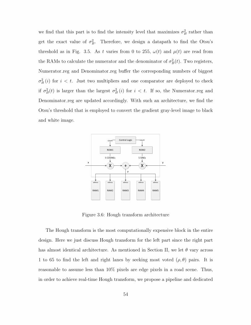
we find that this part is to find the intensity level that maximizes σ2B rather than
get the exact value of σ2B. Therefore, we design a datapath to find the Otsu’s
threshold as in Fig. 3.5. As t varies from 0 to 255, ω(t) and µ(t) are read from
the RAMs to calculate the numerator and the denominator of σ2B(t). Two registers,
Numerator reg and Denominator reg buffer the corresponding numbers of biggest
σ2B (i) for i < t. Just two multipliers and one comparator are deployed to check
if σ2B(t) is larger than the largest σ2
B (i) for i < t. If so, the Numerator reg and
Denominator reg are updated accordingly. With such an architecture, we find the
Otsu’s threshold that is employed to convert the gradient gray-level image to black
and white image.
ROM1
X
ROM2
X
5 COSINEs 5 SINEs
x y
+
RAM1 RAM2 RAM3 RAM4 RAM5
ρ
Control Logic countcount
address address address address address
Figure 3.6: Hough transform architecture
The Hough transform is the most computationally expensive block in the entire
design. Here we just discuss Hough transform for the left part since the right part
has almost identical architecture. As mentioned in Section II, we let θ vary across
1 to 65 to find the left and right lanes by seeking most voted (ρ, θ) pairs. It is
reasonable to assume less than 10% pixels are edge pixels in a road scene. Thus,
in order to achieve real-time Hough transform, we propose a pipeline and dedicated
54
architecture as in Fig. 3.6. ROM1 and ROM2 store cosine and sine values for θ
from 1 to 65 (totally 13 groups with every 5 successive ones as a group). When the
HT module receives position information of edge pixels, it reads out cosine and sine
values of θ and performs Hough transform. Control logic generates a signal count to
indicate which 5 θ′s are being processed. Once they receives the ρ, each block reads
its corresponding value from RAMs, adds it by 1, and then write it back. After
all edge pixels go through the Hough transform module, the system scans all RAM
locations and finds most voted (ρ, θ) pair as the left lane. If the detected lanes are
excessively upright (θ < 30), a lane departure warning will be released at the very
first time.
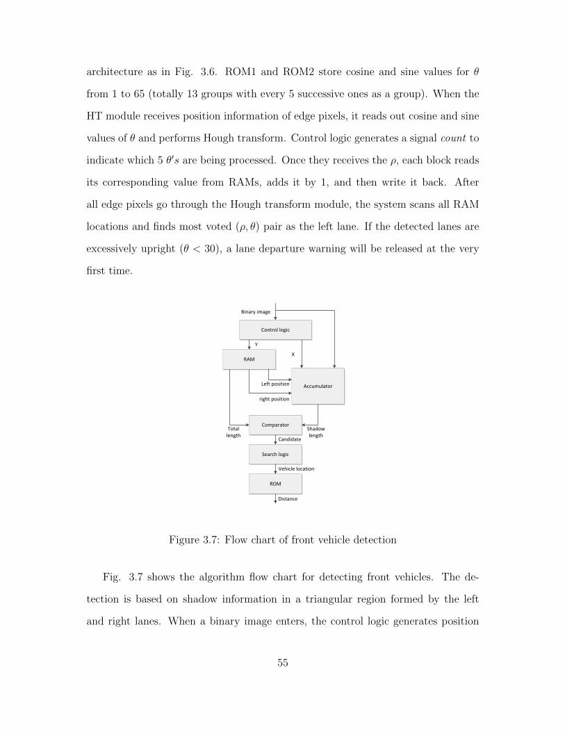
Control logic
Binary image
RAM
Accumulator
Comparator
Search logic
ROM
Y
X
Left position
right position
Total length
Shadow length
Vehicle location
Distance
Candidate
Figure 3.7: Flow chart of front vehicle detection
Fig. 3.7 shows the algorithm flow chart for detecting front vehicles. The de-
tection is based on shadow information in a triangular region formed by the left
and right lanes. When a binary image enters, the control logic generates position
55

information X and Y. For every row, the RAM, as a LUT, provides left and right
boundary positions of a targeted triangle region based on vertical information Y.
The Accumulator block counts the white pixels within the triangle area for each
row. If the number of filled pixels is larger than a fixed ratio to the triangle width
of that row, it is a candidate for front vehicle detection. The candidate row, which
are closest to the bottom of an image, is considered as the front vehicle’s position.
Finally, the system converts the row number to the physical distance on the ground
through a LUT implemented using a ROM. If the vehicle traveling speed is known,
a front collision warning can be issued when the front vehicle is closer than the safe
distance.
3.1.4 Experimental Results
The proposed design is implemented in Verilog HDL. Xilinx ISE tool is used for
design synthesis, translation, mapping and placement and routing (PAR). In order
to validate the entire design, we conduct an experiment on a KC705 FPGA platform.
The video streams from a camera mounted on a vehicle windshield are sent to an
on-board Kintex-7 FPGA via FMC module. The FPGA performs lane departure
and front collision warning examination on every video frame and exports the results
to a monitor for display. The input video is 720P resolution at the rate of 60 fps.
We take the video clock as system clock of our design, which is 74.25MHz in this
case.
Table 3.1: Device utilization summaryResources Used Available UtilizationNumber of Slices Registers: 8,405 407,600 2%Number of Slice LUTs: 10,081 203,800 4%Number of Block RAMs: 60 445 13%Number of DSP48s 31 840 3%
56

The resources utilization of the LDW and FCW systems on an XC7K325TFPGA
is shown in Table 3.1. Although we verify the design on a 7-series FPGA, it can also
be implemented on a much smaller device for lower cost and less power consumption,
e.g. Spartan-6 FPGA. The reported maximum frequency is 206 MHz. Thus if the
system runs at maximum frequency, it can process 720P video at 160 fps, which is
corresponding to the pixel clock frequency at 206 MHz. The design is validated by
road tests using the FPGA-based hardware system. Fig. 3.8 illustrates some results
of our LDW and FCW systems. The detected lanes are marked as green and the
detected front vehicle is marked as blue.
(a)
(b)
(c)
(d)
Figure 3.8: Results of our LDW and FCW systems
57
3.2 Traffic Sign Detection System Using SURF
3.2.1 Introduction
In driver-assistance systems, traffic sign detection is among the most important and
helpful functionalities. Many traffic accidents happen due to drivers’ failure to ob-
serve the road traffic signs, such as stop signs, do not enter signs, speed limit signs,
and etc. Three kinds of methods are often applied to implement road traffic sign de-
tection – color-based, shape-and-partition-based, and feature-based algorithms[11].
Traffic signs are designed with unnatural color and shape, making them conspic-
uous and well-marked. Color-based and shape-based method are the initial and
straightforward ones to be used for sign detection[12][13]. However, these methods
are sensitive to the video environment. Illumination change and partial occlusion of
traffic sign seriously degrade the effectiveness of these methods. The third type of
methods are based on feature extraction and description. These algorithms detect
and describe salient blob as features of an image and video. The features are usually
unaffected by the variance of illumination, position and partial occlusion. Reported
feature-based algorithms contain Scale Invariant Feature Transformation (SIFT)[14],
Histogram of Oriented Gradient (HoG)[15], Haar-like feature algorithm[16], etc.
Speeded Up Robust Features (SURF) [17] is one of the best feature-based algo-
rithms and has found wide application in the Computer Vision community[18][19][20].
It extracts Hessian matrix-based interest points and has a distribution-based de-
scriptor, which is a scale- and rotation-invariant algorithm. These features make it
perfect for object matching and detection. The key advantage of SURF is to use
integral image and Hessian matrix determinant for feature detection and descrip-
tion, which greatly boosts the process efficiency. Even so, like other feature-based
algorithms, SURF is computationally complex which often results very low frame
58

rate on an embedded processor. In order to employ SURF for real-time appli-
cations, parallel processing architecture and platform need to be considered. By
analyzing the parallelism during each step of the SURF algorithm, we choose Field
Programmable Gate Array (FPGA) as the embedded platform because of its rich
resources for computations and convenient access of local memories. Finally, we
implement a SURF-based real-time road traffic sign detection system on a Xilinx
Kintex-7 FPGA with SVGA video input and output.
3.2.2 SURF Algorithm
This section overviews the SURF algorithm [17]. The algo-rithm consists of three
main steps: integral image generation, interest point localization, and interest point
description.
I∑ (P ) =x∑
i=0
y∑j=0
I(x, y) (3.9)
Integral image is one of the main advantages of SURF. Integral image I∑ (P )
in P = (x, y) represents the sum of all the pixels on the left and top of P as in
(3.9). Integral image is used in both the subsequent interest point detection and
description to obtain higher efficiency. Once integral image is computed, it takes
only 3 additions/subtractions to get the sum of the pixels intensities over an upright
rectangular region. Another benefit is that the calculation time is independent of
the box size.
SURF detector locates features based on the Hessian matrix. The original defi-
nition of Hessian matrix is shown in (3.10),
59
H (P, s) =
Lxx (P, s) Lxy (P, s)
Lxy (P, s) Lyy (P, s)
(3.10)
where Lxx (P, s) denotes the convolution of Gaussian second-order derivative in x−
direction with input image in point P at scale s, and similarly for Lxy (P, s) and
Lyy (P, s). Simple box filters using the integral image are used to approximate
the second-order Gaussian partial derivation, and yielding less computation bur-
den. The problem thus reduces from calculating Gaussian second-order derivative
responses to the box filter responses. Denoting the blob responses by Dxx, Dyy and
Dxy , then the determinant of the original Hessian matrix in SURF is approximated
as follows:
det(Happrox) = DxxDyy − (0.9Dxy)2 (3.11)
where 0.9 is used to balance the Hessian determinant. In order to achieve scale
invariance, SURF applies box filters of different sizes on the original image to search
and compare interest points. Box filters of different sizes construct the scale space,
which is divided into octaves. The local maxima of box filter responses larger than
a predefined threshold in image and scale space are selected as interest point candi-
dates. A non-maximum suppression in a 3×3×3 neighborhood is applied to screen
out “false” candidates with position correction elements above 0.5 and localize in-
terest points.
SURF builds an descriptor around the neighborhood of each interest point. First,
a square region of 20s-by-20s centered on the interest pointis constructed along the
dominant direction. In order to keep it simple, the dominant directions of interest
points are set to be upright. The region is then divided into 4×4 smaller sub-regions
with each window size 5s-by-5s (sampling step s). For each of these sub-regions,
60

Haar wavelet responses (filter size 2s) are computed at 5 × 5 regularly distributed
sample points. These responses are then weighted by a Gaussian function(σ = 3.3)
centred at the interest point. We use dx and dy to denote weighted Haar wavelet
response in horizontal direction and vertical direction. Each sub-region generates a
4-D vector v = (∑dx,
∑dy,
∑|dx|,
∑|dy|). All sub-regions are then concatenated
into a vector, resulting in a 64-dimensional descriptor vector.
3.2.3 FPGA Implementation of SURF
The SURF algorithm introduced in Section 3.2.2 is considered as a high-speed,
robust and accurate method to extract and describe interest points of an image or
a video frame. Descriptors of these key points can be used as pivotal features of
images and videos, and can be applied in many applications, such as traffic sign
detection, machine stereo vision, object tracking, etc. However, the complexity of
the algorithm itself leads to frequent memory access and long computing latency,
which makes the SURF algorithm difficult to be used in real-time systems. On
a dual-core 2.5 GHz processor,simulations of the Matlab code configured with the
first two octaves takes 1.38 seconds to detect and describe all the 284 feature points
from an image with 800×600 resolution. More recently, an FPGA SoC architecture
was proposed and it achieved about 10 fps processing rate on a Xilinx XC5VFX70
FPGA incorporating PowerPC-440 CPU with floating-point processing units [21].
It was an approach of hardware/software co-design with integral image generator
and fast-Hessian generator implemented by dedicated hardware, and the rest of
the algorithm was implemented using software of the embedded PowerPC. But the
frame rate is still unsatisfactory for real-time systems like traffic sign detection.
This section presents a FPGA-only architecture to implement the real-time
SURF algorithm toward videos in 800×600 resolution at 25 fps. We will first present
61

the overall system architecture using data flow and state the limitation and approx-
imation of the FPGA implementation. Then we will describe each function module
in detail.
3.2.3.1 Overall system architecture
We make every effort to follow the original SURF algorithm as closely as possible.
However, we still have to do several approximations for the hardware design. Firstly,
traffic sign usually occupies only a small part of a frame, which makes most of interest
points detected at the first two octaves with small filter sizes. Based on this, the
hardware architecture computes the fast-Hessian responses of pixels and detects the
interest points among them only at the first two octaves. The filter size at octave 1
is 9, 15, 21, 27 while octave 2 contains 15, 27, 39, 51. Initial sample rate of octave
1 is set to 2. The current design is oriented towards videos in 800×600 resolution
at 25 fps and it can be easily adapted to other sizes. Secondly, as mentioned in
Section 2, the dominant direction of each interest point is set upright to simplify
calculation. Finally, we implement a modified descriptor using larger, overlapping
sub-regions to ensure better matching performance.
DDR-3 SDRAM
Physical
Interface
Integral
Image
Generator
Interest
point
detector
Interest point
descriptor
Kintex 7 FPGA
Video
In
Video
Out
Memory Controller Module
Interest Points
Index & Scale
Integral
Image
Interest Points
Surroundings
Xilinx FPGA MIG Solution
Integral
Image
Figure 3.9: Overall system block diagram
The overall system diagram is summarized in Fig. 3.9. The FPGA-based SURF
architecture is composed of 4 submodules - Integral Image Generator, Interest Point
62

Detector, Interest Point Descriptor and Memory Controller Module. The input is
RGB format video with 40M pixel rate. Integral Image Generator converts the
original data to gray integral image and transfers it to Interest Point Detector and
Memory Controller Module. Interest Point Detector is aimed to find all the local
Fast-Hessian maxima as interest points and get their index and scales. Memory
Controller Module is designed for data writing and reading with SDRAM interface.
It stores the integral image and provides the integral image of interest points sur-
roundings to the Interest Point Descriptor. In addition, a comparator module (not
shown because it is independent of SURF) matches the interest points descriptors of
the current frame with those of the library to determine if a traffic sign is detected.
In the video output, the traffic sign is highlighted before sending to the display. The
details of each module are explained below.
3.2.3.2 Integral image generation
RGB2GRAYaddress
generationaccumulation
24-bitRGBpixel
8-bitGraypixel
8-bitGraypixel
28-bitintegral
pixel
Controlsignals
Controlsignals
Controlsignals
andaddress
Controlsignals
Figure 3.10: Integral image generation block diagram
Integral image generation module is the entry point of the entire architecture.
Its block diagram is shown in Fig. 3.10. It consists of 3 lower-level modules. The
input video data is in RGB format while all the SURF calculation is based on gray
scale. The RGB2GRAY unit is responsible for this transformation. After that, row
and column information is produced according to control signals (vsync, hsync and
de) in address generation module. Finally, an integral image is calculated in the
accumulation module. Suppose the current video position is D, its integral image
63

can be obtained from ID = IA + iD − IB − IC , where I denotes integral image and
i the gray value. A,B,C are the upper-left, upper and left pixel of D, respectively.
To reduce register uses, the integral image of upper line is stored in a block ram.
It is also noted that the video of integral image has the same format with the
original one. The only difference is that the 24-bit RGB information is replaced by
a 28-bit gray integral value.
3.2.3.3 Interest points detector
This module is designed to calculate fast-Hessian responses of all sample points
at multi-scale and then find local maxima at x, y and scale space as interest
point candidates. A non-maximum suppression is applied to these candidates to
screen out “false” interest points. Interest points detector is divided into 3 blocks:
Build Hessian Response, Is Extreme and Interpolate Extremum. They are explained
as follows.
Build Hessian Response Build Hessian Response block diagram is shown in
Fig. 3.11. The largest filter size among the first 2 octaves is 51. According to
SURF algorithm, integral image located in the rectangle with relative location be-
tween (-26,-26) and (25,25) are needed to calculate responses of all Gaussian filter
size of the first 2 octaves. In our design, the initial sampling step is defined as 2 and
octave 2 doubles that. Therefore, iterative cycle is 4 lines. Calculation of filter size
of octave 1 is carried out in line 1, 3, 5, 7, etc, while that of octave 2 in line 1, 5, 9, 13,
etc. Based upon these analysis, this block utilizes 56 block RAMs with depth of 800
to buffer 56 integral image lines. Each Block RAM can be accessed independently.
600 lines of integral image are stored into the 56 Block RAM iteratively. This archi-
tecture makes the writing of incoming pixels and calculation of Gaussian response
64

RGB2GRAYaddress
generationaccumulation
24-bitRGBpixel
8-bitGraypixel
8-bitGraypixel
28-bitintegral
pixel
Controlsignals
Controlsignals
Controlsignals
andaddress
Controlsignals
Figure 3.11: Build Hessian Response block diagram
happen concurrently. For example, the incoming integral image pixel of line 53 is
stored into Block RAM 53 while the first 52 image lines are all available for Gaus-
sian response calculation of octave 1 and octave 2. 100 MHz clock frequency ensures
the pace of 192 pixels (due to overlap, it is actually 164 pixels) access for the re-
sponse computation of 6 different filter size. In addition, Pre BRAM FIFO buffers
incoming integral image at 40 MHz pixel rate and delivers the data at 100 MHz
system clock. Hessian Response Computation is the pipelined calculation unit of
fast-Hessian determinant response. To save DSP resources of FPGA, 192 pixels are
serialized into 6 groups. After calculation, 6 Hessian determinants are de-serialized
and transferred to Is-Extreme block in parallel.
Is Extreme Is Extreme unit (in Fig. 3.12) is aimed to find local maxima of
Hessian-matrix determinants as interest points candidates. With the incoming first
two octaves response, local maxima can be detected on layers with filter size of 15,
65
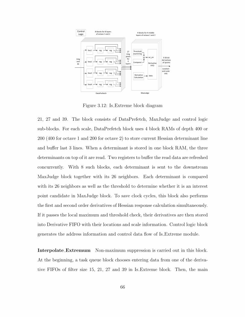
line1
Control Logic
reg reg
line2 reg reg
line3 reg reg
line4 reg reg
Thresholdexamining
DerivativeCalculation
DerivativeFIFO
8 blocks for 8 layers of octave 1 and 2
4 blocks for 4 middle layers of octave 1 and 2
iimgandde
27 iimg
pixelsfor4
layers
wr_en
data
x 9 30-bit derivatives of ipoints
Location and scale
info
Comparer
DataPrefetch MaxJudge
Figure 3.12: Is Extreme block diagram
21, 27 and 39. The block consists of DataPrefetch, MaxJudge and control logic
sub-blocks. For each scale, DataPrefetch block uses 4 block RAMs of depth 400 or
200 (400 for octave 1 and 200 for octave 2) to store current Hessian determinant line
and buffer last 3 lines. When a determinant is stored in one block RAM, the three
determinants on top of it are read. Two registers to buffer the read data are refreshed
concurrently. With 8 such blocks, each determinant is sent to the downstream
MaxJudge block together with its 26 neighbors. Each determinant is compared
with its 26 neighbors as well as the threshold to determine whether it is an interest
point candidate in MaxJudge block. To save clock cycles, this block also performs
the first and second order derivatives of Hessian response calculation simultaneously.
If it passes the local maximum and threshold check, their derivatives are then stored
into Derivative FIFO with their locations and scale information. Control logic block
generates the address information and control data flow of Is Extreme module.
Interpolate Extremum Non-maximum suppression is carried out in this block.
At the beginning, a task queue block chooses entering data from one of the deriva-
tive FIFOs of filter size 15, 21, 27 and 39 in Is Extreme block. Then, the main
66

computation is to perform the matrix operation as in (3.12).
O = −H\D
= −
H11 H12 H13
H21 H22 H23
H31 H32 H33
\D1
D2
D3
= − 1
det(H)·
H∗11 H∗12 H∗13
H∗21 H∗22 H∗23
H∗31 H∗32 H∗33
·D1
D2
D3
(3.12)
where det (H) = H11 ×H∗11 +H12 ×H∗12 +H11 ×H∗12.
the companion matrix H∗ijis shared by numerator and denominator calculation.
Considering enormous resources demanding of division, only fraction1
det(H)is com-
puted to transform other arduous division to multiplication. The absolute value of
matrix O elements should be less than 0.5 so that the local maximum is accepted as
interest point. The x, y and scale of interest points are then adjusted accordingly.
3.2.3.4 Memory management unit
A frame with 800×600 resolution is too large for on-chip block RAM and can only be
stored in on-board SDRAM. Xilinx provides designers the 7 Series FPGA Memory
Interface Generator (MIG) to communicate with off-chip DDR3 SDRAM. It wraps
the complex physical signals of DRAM and provides an easily-access user interface.
The user interface runs at 200 MHz clock with 512-bit data width. In our design,
this unit manages all memory access, and plays the role of a bridge between interest
point detector and interest point descriptor. It performs the following functions:
1. de-serializing 8 successive integral image points and writing them into the MIG
and SDRAM. A clock domain crossing FIFO is deployed to interface between
67

40 MHz pixel rate to 200 MHz data rate.
2. generating the addresses of interest point surroundings of the rectangle be-
tween (-13s, -13s) and (12s, 12s) with interval s, where s is the scale. Then
read command is applied to MIG with desired pixels addresses. Due to the
single port property, we grant write command with higher priority than read
command.
3. when all the surroundings of an interest point, 26 × 26 integral image pixels,
are available, transferring them to Interest Point Descriptor module serially
with index and scale information of current interest point. The clock domain
crossing between 100 MHz system clock and 200 MHz MIG UI clock is also
implemented by independent clock FIFO.
3.2.3.5 Interest point descriptor
Haar wavelet transform
Wavelet response reconstruct
Gaussian mask controller
Gaussian mask weight
Gaussian mask LUT
Sub-regions accumulation
Gaussian scaling
Accumulation for length of
regionnormalization
26x26 iimg
scale
28 bits
32 bits24x24 Haar
wavelet response
Gaussianmask
32 bits
Sub-region wavelet response
32 bits
16x2 response block channels for
X and Y dir
32 bits
36 bits 16x2 Gaussian weight results
48 bits16x4 Sub-region pre-descriptor
36 bits
48 bits64-dimensional
descriptor
Figure 3.13: Interest point descriptor block diagram
68
Unlike original SURF implementation, modified SURF calculates descriptor from
a square region with edge size of 24s. Equally, this rectangle is split up to 16 sub-
region. Each sub-region is 9s×9s. Adjacent sub-regions have overlap of 9×4 points.
To perform modified SURF descriptor computation, a 26 × 26 matrix needs to be
extracted from the integral image to calculate the 2D Haar wavelet transform. The
block buffers 3 lines of serial-coming integral image pixels to calculate Haar wavelet
response of the central lines. After that, the 24× 24 responses are reconstructed as
16 9× 9 sub-block. We use Gaussian mask to weight each sub-block and obtain 16
dx and dy simultaneously. Gaussian mask of possible scales has been pre-calculated
and loaded to look up table during the initial stage. After that, we sum dx, dy
and |dx|, |dy| of all 16 sub-regions respectively and get the pre-descriptor. The pre-
descriptor is organized as a 64 × 1 vector. Finally, the pre-descriptor is Gaussian-
scaled and normalized to get the final descriptor for a precise matching result. An
accumulation unit is used to compute normalization factor. Fig. 3.13 shows key
design details, such as data flow and bus width, that are important to achieve real-
time performance.
3.2.3.6 Descriptor Comparator
After interest point descriptors calculation, the comparator computes the similarity
of current frame and pre-built traffic sign libraries to determine whether a traffic
sign is detected. As an initial experiment, the system stores only stop signs in the
library using on-chip block RAM. We choose 128 representative interest points in
the standard stop sign image, then calculate their descriptors for the library.
When the descriptor of an interest points enters this module, the comparator
reads descriptors of interest points in the library for matching. The entering de-
scriptor needs to be matched with every descriptor in the library. The speed is un-
69

acceptable if the match is conducted completely serially. As a tradeoff between speed
and resource use, the 128 descriptors are divided into 8 independent groups. The
groups are matched with the current descriptor concurrently while 16 descriptors in
a group enter in pipeline mode. This architecture improves processing performance
considerably.
A descriptor subtracting 128 library descriptors produces 128 distance values.
After all the interest point descriptors are processed, this module generates a 128
distance vectors. The 128 vectors are sorted and the system chooses sum of the
smallest 30 ones to compare with the threshold. If the sum is less than the threshold,
then a stop sign is detected.
3.2.4 Results
We build the system on a Kintex-7 FPGA board shown in Fig. 3.14. The video
frames are sent to a Xilinx KC705 platform through the AVNET video I/O board on
the FMC connector. FPGA detects traffic signs of every video frame and output the
video for display using the same adaptor. Table 3.2 presents the design summary
on Kintex 7 FPGA. The maximum frequency is 125.92 MHz (the Xilinx memory
interface IP core runs independently at a separate 200 MHz clock zone). All timing
constraints are met. The test frame rate is 60 fps of 800 × 600 resolution. The
FPGA-SURF implementation achieves real-time while producing the same results in
video stream as original CPU-based SURF, thus very promising for future industry
application.
70

Figure 3.14: Traffic sign detection system
Table 3.2: Device utilization summaryResources Used Available UtilizationNumber of Slices Registers: 108,581 407,600 26%Number of Slice LUTs: 179,559 203,800 88%Number of RAM36s: 182 445 40%Number of RAM18s: 80 890 8%Number of DSP48s 244 840 29%
3.3 Traffic Sign Detection System Using SURF
and FREAK
In our previous work [1], the SURF algorithm is used because it employs integral
image to quickly search blob-like keypoints by detecting local maxima of Hessian
matrix determinant. However, the calculation and matching of SURF descriptors
cost much computational and memory resources. In this paper, we adopt the state-
of-the-art FREAK descriptor to replace the SURF descriptor in [1].
Inspired by human visual system, FREAK produces a cascade of binary strings
as the keypoint descriptor. The binary structure makes the descriptor faster to
compute and easier to match, while remaining robust to scale, noise and rotation.
To the best of our knowledge, this is the first hardware implementation of FREAK
on an FPGA. Our experimental results demonstrate that the FPGA-based design
71

is fully functional and it achieves the real-time performance of processing videos of
800×600 resolution at 60 frame-per-second (fps), while the software implementation
on Intel Core i5-3210M CPU achieves only about 2.5 fps using the same algorithms.
3.3.1 FREAK Descriptor
For every keypoint detected by SURF detector, FREAK generates a binary de-
scriptor that compares 43 weighted Gaussian average over sampling points near the
keypoint. Fig. 3.15 shows the FREAK sampling pattern. The sampling pattern
is biologically inspired by human retina sampling grid which is circular with the
difference of having higher density of sampling points near the central keypoint. In
order to make the descriptor less sensitive to noise, all sampling points need to be
smoothed with Gaussian kernel. By mimicking the retina pattern, FREAK applies
different kernels size on the sampling points. The closer to the center, the smaller
kernel size is used.
Figure 3.15: Illustration of the FREAK sampling pattern
FREAK constructs the binary descriptor string S by one-to-one comparison of
the smoothed sampling point:
S =∑
0≤a≤N
2aT (Pa) , (3.13)
72

where Pa is a pair of sampling points, N is the length of the descriptor string,
and
T (Pa) =
1
0
if M (P r1a ) > M (P r2
a ) ,
otherwise,
(3.14)
with M (P r1a ) and M (P r2
a ) are the smoothed intensity of sampling points of the
pair Pa.
Instead of comparing each sampling point with all others, FREAK produces a
512-bit descriptor by comparing 512 most important pairs. The 512 bits are further
separated to 4 components each with 128-bits, which represents a coarse-to-fine
information architecture, to speed up the matching processing.
3.3.2 Hardware Implementation
This section presents the FPGA design to implement real-time object detection
using SURF detector and FREAK descriptor on a Xilinx KC705 board. The design
is aimed to process videos of 800× 600 resolution at 60 fps and detect 10 different
kinds of objects simultaneously. We first introduce the overall system architecture,
and then describes each module in detail.
3.3.2.1 Overall System Architecture
Fig. 3.16 shows the overall system architecture that is composed of 5 sub-modules.
As the entry module, Integral Image Generator converts RGB format video pixels to
grayscale and accumulates them to get the integral image. Interest Point Detector
finds all blob-like keypoints using SURF. Keypoint descriptor calculation is per-
formed in FREAK Descriptor module. Memory Management Unit is responsible for
73

SDRAM
Interest point Detector
FREAK Descriptor
Kintex 7 FPGA
VideoIn
Memory Management Unit
Keypoints location & scale
Integral Image
Xilinx FPGA MIG Solution
Integral Image
Descriptor Matching
Sampling points surroundings
Result
KeypointDescriptor
Integral Image
Generator
Figure 3.16: FPGA design system block diagram
integral image storage and access. Finally, Descriptor Matching Module performs
the keypoint descriptor matching and produces traffic sign detection results.
3.3.2.2 Integral Image Generator and Interest Point Detector
The design of these two modules are similar to our previous implementation in [1].
Integral Image Generator has three lower-lever blocks which implement RGB to
grayscale transformation, address generation and integral image calculation, respec-
tively. Interest Point Detector also consists of three functional blocks: Build Hessian Response,
Is Extreme and Interpolate Extremum. An independent clock FIFO first trans-
fers 40 MHz integral image pixel rate to 100 MHz system clock domain. Then,
Build Hessian Response uses a Block RAM ping-pong structure to fetch necessary
integral image pixels and calculates box filter responses of the first two octaves of the
scale space in pipeline mode. Is Extreme employs an buffer to obtain every box filter
response together with its 26 neighbors in x, y and scale space at the same time, and
then finds all local maxima as keypoint candidates. Interpolate Extremum carries
out non-maximum suppression to filter out false keypoint candidates. More details
can be found in [1].
74

3.3.2.3 Memory Management Unit
Integral image with 800× 600 resolution is too large for the FPGA on-chip BRAM,
and thus can be only stored in off-chip SDRAM. Memory Management Unit is re-
sponsible for writing integral image to SDRAM via FPGA Memory Interface Gen-
erator (MIG) IP core and generating addresses of integral image, which are required
for descriptor calculation, to read data back from SDRAM. In our design, we take
the average of a square patch for every sampling point, instead of using Gaussian
approximation. Thus the integral image, which is obtained in previous step, further
accelerates the calculation of smoothed sampling points intensities. Both the dis-
tances of sampling points to keypoint and the sizes of square patches are related to
keypoint scale. In order to save computational resources, we also quantize possible
keypoint scales to 64 levels and compute the corresponding distances and square
sizes in advance. These data are stored in SRAM for lookup in subsequent steps.
Fig. 3.17 illustrates how this module generates correct addresses from keypoint
locations and scales using the SRAM. (X left, Y top), (X right, Y top), (X left,
Y bottom) and (X right, Y bottom) are locations of 4 vertices of the square patch
for each sampling point.
SRAM
+
+ +
+
-
-
Keypoint x
Keypoint y
KeypointScale
dx
dy
Square size
Sampling point x
Sampling point y
X_right
X_left
Y_top
Y_bottom
Figure 3.17: Integral image address generator.
75

3.3.2.4 FREAK Descriptor
SRAM
-
x
area
1/area
Normalized intensity
Sum of intensities over the square
X_right
X_left
Y_bottom
Y_top
x-
-ID
--
IC
IB
IA
Figure 3.18: Normalized intensity calculation.
It requires four integral image pixels for a smoothed retina point intensity cal-
culation, namely IA, IB,IC ,and ID. It then involves a division operation to obtain
the normalized sampling point intensity as in (3.15).
M =ID − IC − IB + IA
area, (3.15)
However, dividers are expensive for FPGA implementation in term of hardware
resource and latency, and should be avoided if possible. In our design, Fig. 3.18
shows an alternative method to compute the smoothed sampling point intensity.
First, the area of the square patch is calculated. Then, a look-up table (LUT) is
used to get the reciprocal of the area. Meanwhile, the sum of pixels intensities in the
square is quickly obtained using integral image. Finally the normalized sampling
point intensity is obtained from a multiplication.
For object detection applications, image content has little impact on the selected
pairs. We conduct an experiment in advance to find the 512 most important pairs
and their indices. With all 43 smoothed sampling points intensities, this module
takes advantage of 512 pairs indices to build a cascade of 512-bit binary string as
76

the keypoint descriptor.
3.3.2.5 Descriptor Matching Module
SRAM
XOR
Count 1s of each 128 bits and get a 4D vector
Output 1 only if each element of the vector is smaller than a
distance threshold
Matching sign of each interest point in the library
OR
If the matched pairs number is larger than a pre-set threshold,
corresponding object is detected
Descriptors in library
Descriptors of video frame
Figure 3.19: Descriptor matching flow chart
Once the FREAK keypoint descriptors are generated, the Descriptor Matching
Module compares them with the precomputed descriptors of the traffic signs in the
library. It effectively quantifies the similarity between the traffic signs detected in the
current video frame and each traffic sign in the library. In our design, the system is
aimed to detect 10 different kinds of traffic signs in the picture and thus 10 descriptor
matching units are instantiated for the parallel comparison. The architecture and
flow chart of the descriptor matching is shown in Fig. 3.19. For each desired
traffic sign in the library, we find 500 representative keypoints and then calculate
the FREAK descriptors for each keypoint. These descriptors are stored in on-chip
SRAM as the library.
When processing each video frame, the descriptor of an keypoint is computed
and is entered into the descriptor matching unit that reads the descriptors from
77

the library for one-to-one comparison. We compare every 128-bits of the 512-bit
descriptor between the evaluated keypoint and the keypoints in library. Only if
all four distances are smaller than a threshold, we set the matching status of the
keypoint as true. It indicates a good match for the keypoint is found in the library.
Initially, the values of all matching results are set to false. After all the keypoints are
processed, the output module counts the number of keypoints whose matching status
bits are set as “true”. If the total number is larger than an empirical threshold, then
a corresponding traffic sign is detected. With a set of 10 parallel matching units, the
system is able to detect 10 different traffic signs concurrently and independently.
3.3.3 Results
In order to validate the FPGA design, we setup an experiment to detect 10 different
traffic signs in a video stream. The video are compared with standard traffic sign
images frame by frame, whose features are precomputed and stored in the library
in the on-chip BRAM. The target platform is Xilinx KC705 evaluation board. The
video streams from a camera are sent to the FPGA through an FMC video adaptor
with HDMI input. FPGA performs traffic sign detection of every video frame and
exports the results to 10 LEDs for display. The target frame rate is 60 fps for image
resolution of 800×600. The entire system architecture is designed and implemented
using Verilog HDL.
Table 3.3: Device utilization summaryResources Used Available UtilizationNumber of Slices Registers: 60,044 407,600 14%Number of Slice LUTs: 147,190 203,800 72%Number of RAM36s: 289 445 64%Number of RAM18s: 321 890 36%Number of DSP48s 139 840 16%
78

Figure 3.20: A matching example of STOP sign detection
The resources utilization of the traffic sign detection and recognition system on
FPGA is listed in Table 3.3. The maximum frequency is 122 MHz. In order to verify
the design, the same algorithm is implemented on software running on a CPU. The
FPGA hardware produces exactly the same results as the software. In addition, the
FPGA system successfully detects the traffic signs at 60 fps, which is sufficient for
real-time applications. As an example, Fig. 3.20 shows the matching result of a
video frame with a standard STOP sign.
3.4 Summary
In this chapter,we build complex video processing systems design and analyze the
result on hardware. We implement the entire system, including video input, video
processing and video display, for real time video applications: lane departure warn-
ing/ front collision warning system and traffic sign detection system. The results
prove that our systems could handle complicated high-throughput video processing
with real-time requirement.
79

Chapter 4
Conclusions
In this thesis, we focus on real-time video/image processing. At begining, we intro-
duce basic concepts of digital image/video and how to perform basic and fundamen-
tal operations on image/video in Matlab environment. When the image/video size
goes large, as today’s HD and Ultra HD resolution, it’s almost impossible to process
and analyze an ocean of video/image data fastly enough. We employ FPGA, owing
natural parallel computing architecture and easy access to local memory, to accel-
erate image/video processing in real time. However, FPGA development is always
time and energy cosuming compared to software development.
Furtunately, Mathworks provide HDL coder toolbox, which supports HDL code
generation for Matlab and Simulink and provide entire workflow for programming
FPGA boards. We make 8 demos to show building demos in Simulink and translate
Simulink blocks to HDL code that could directly run on FPGA.
Besides, We present two function blocks of advanced driver assistance system -
traffic sign detection and lane departure warning/ front collision warning system, as
examples to demostrate powerfulness of advanced image/video processing on FPGA,
especially for those scenarios having real-time demand.
80

We are glad to find that our FPGA solution achieves the speedup of over 10
times faster than traditional CPU platform for image/video processing.
In conclusion, FPGA accelerations is a cost-efficient, high-performance video
processing solution for those applications with low power and real-time requirements.
81

Bibliography
[1] J. Zhao, S. Zhu, and X. Huang, “Real-time traffic sign detection using surf fea-tures on fpga,” in High Performance Extreme Computing Conference (HPEC),2013 IEEE. IEEE, 2013, pp. 1–6.
[2] A. Broggi, C. Caraffi, R. Fedriga, and P. Grisleri, “Obstacle detection withstereo vision for off-road vehicle navigation,” in Computer Vision and PatternRecognition - Workshops, 2005. CVPR Workshops. IEEE Computer SocietyConference on, 2005, pp. 65–65.
[3] D. M. Gavrila, “Pedestrian detection from a moving vehicle,” in ComputerVision, ECCV 2000. Springer, 2000, pp. 37–49.
[4] R. Marzotto, P. Zoratti, D. Bagni, A. Colombari, and V. Murino, “A real-timeversatile roadway path extraction and tracking on an fpga platform,” ComputerVision and Image Understanding, vol. 114, no. 11, pp. 1164–1179, 2010.
[5] R. Risack, N. Mohler, and W. Enkelmann, “A video-based lane keeping as-sistant,” in Intelligent Vehicles Symposium, 2000. IV 2000. Proceedings of theIEEE. IEEE, 2000, pp. 356–361.
[6] J. C. McCall and M. M. Trivedi, “Video-based lane estimation and tracking fordriver assistance: survey, system, and evaluation,” Intelligent TransportationSystems, IEEE Transactions on, vol. 7, no. 1, pp. 20–37, 2006.
[7] W. Wang and X. Huang, “An fpga co-processor for adaptive lane departurewarning system,” in Circuits and Systems (ISCAS), 2013 IEEE InternationalSymposium on. IEEE, 2013, pp. 1380–1383.
[8] S. Lee, H. Son, and K. Min, “Implementation of lane detection system usingoptimized hough transform circuit,” in Circuits and Systems (APCCAS), 2010IEEE Asia Pacific Conference on. IEEE, 2010, pp. 406–409.
[9] H.-Y. Lin, L.-Q. Chen, Y.-H. Lin, and M.-S. Yu, “Lane departure and frontcollision warning using a single camera,” in IEEE International Symposiumon Intelligent Signal Processing and Communication Systems (ISPACS 2012),2012.
82

[10] W. Jianlai, Y. Chunling, Z. Min, and W. Changhui, “Implementation of otsu’sthresholding process based on fpga,” in Industrial Electronics and Applications,2009. ICIEA 2009. 4th IEEE Conference on. IEEE, 2009, pp. 479–483.
[11] K. Brkic, “An overview of traffic sign detection methods,” Department of Elec-tronics, Microelectronics, Computer and Intelligent Systems Faculty of Electri-cal Engineering and Computing Unska, vol. 3, p. 10000.
[12] L.-W. Tsai, J.-W. Hsieh, C.-H. Chuang, Y.-J. Tseng, K.-C. Fan, and C.-C. Lee,“Road sign detection using eigen colour,” IET computer vision, vol. 2, no. 3,pp. 164–177, 2008.
[13] A. De La Escalera, L. E. Moreno, M. A. Salichs, and J. M. Armingol, “Roadtraffic sign detection and classification,” Industrial Electronics, IEEE Transac-tions on, vol. 44, no. 6, pp. 848–859, 1997.
[14] D. G. Lowe, “Distinctive image features from scale-invariant keypoints,” Inter-national journal of computer vision, vol. 60, no. 2, pp. 91–110, 2004.
[15] Q. Zhu, M.-C. Yeh, K.-T. Cheng, and S. Avidan, “Fast human detection usinga cascade of histograms of oriented gradients,” in Computer Vision and PatternRecognition, 2006 IEEE Computer Society Conference on, vol. 2. IEEE, 2006,pp. 1491–1498.
[16] M. J. Jones and P. Viola, “Robust real-time object detection,” in Workshop onStatistical and Computational Theories of Vision, 2001.
[17] H. Bay, A. Ess, T. Tuytelaars, and L. Van Gool, “Speeded-up robust features(surf),” Computer vision and image understanding, vol. 110, no. 3, pp. 346–359,2008.
[18] Z. Zhang, C. Cao, R. Zhang, and J. Zou, “Video copy detection based onspeeded up robust features and locality sensitive hashing,” in Automation andLogistics (ICAL), 2010 IEEE International Conference on. IEEE, 2010, pp.13–18.
[19] M. Zhou and V. K. Asari, “Speeded-up robust features based moving objectdetection on shaky video,” in Computer Networks and Intelligent Computing.Springer, 2011, pp. 677–682.
[20] A. C. Murillo, J. Guerrero, and C. Sagues, “Surf features for efficient robotlocalization with omnidirectional images,” in Robotics and Automation, 2007IEEE International Conference on. IEEE, 2007, pp. 3901–3907.
[21] J. Svab, T. Krajnık, J. Faigl, and L. Preucil, “Fpga based speeded up robustfeatures,” in Technologies for Practical Robot Applications, 2009. TePRA 2009.IEEE International Conference on. IEEE, 2009, pp. 35–41.
83