· web view... (of course this extra power has to come from somewhere and that somewhere is an...
TRANSCRIPT
1
5. Bipolar Junction Transistors I
5.1 Basic Transistor Operation
Most students suffer when encountering BJT transistors for the first time for several reasons: (i) they are more complicated than anything you’ve discussed so far; (ii) like diodes, they are non-linear devices, but unlike diodes they are 3-terminal devices…not 2; (iii) they are active devices…they can produce an output containing more power than the input (of course this extra power has to come from somewhere and that somewhere is an external power supply); (iv) their input impedance is low and their output impedance is large. This last fact determines how a transistor must be biased…as we’ll soon see in the following examples.
It is important that you acquire an understanding of transistors…how they work and how they’re typically used. Transistors are essential components of every electronic circuit from the simplest amplifier to the most elaborate digital computer. Integrated Circuits (IC’s), which have mostly replaced individual transistors, are themselves nothing other than huge arrays of transistors (along with other components), over the years each one having been reduced to microscopic size. Still, you have to connect individual IC’s together, to other types of circuits and interface them to the outside world. Thus, you need to understand their input and output characteristics, ratings and how not to mistreat them!
In this lecture, we will by-pass the physics of semiconductors…nor will we present a detailed mathematical analysis of transistor
2
behavior. Most electrical engineering books generate equivalent circuits of transistor operation based on something called the h-parameter (hybrid) model…a presentation that is completely devoid of intuition. Instead, we’ll present a very simple model of transistor behavior, which is highly intuitive and makes them easy to use. Of course there will be limitations with such an approach, but if you want to get into the nuances of semiconductor behavior…take a class in solid state physics or electrical engineering.
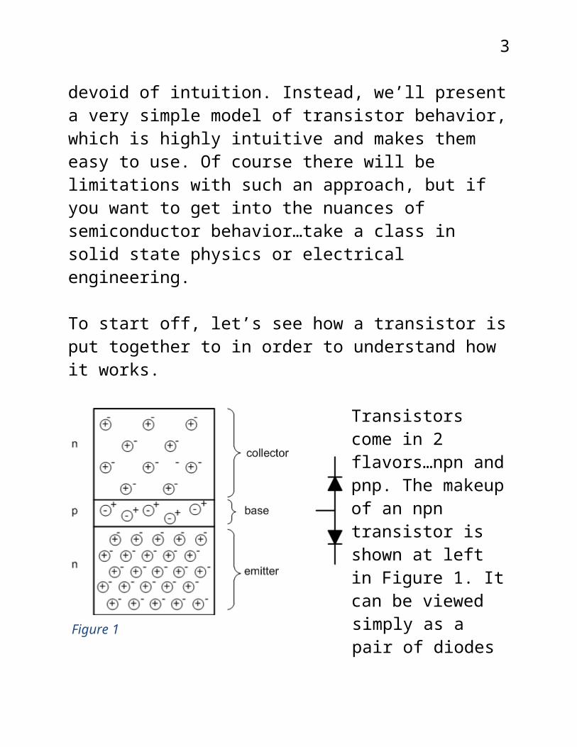
To start off, let’s see how a transistor is put together to in order to understand how it works.
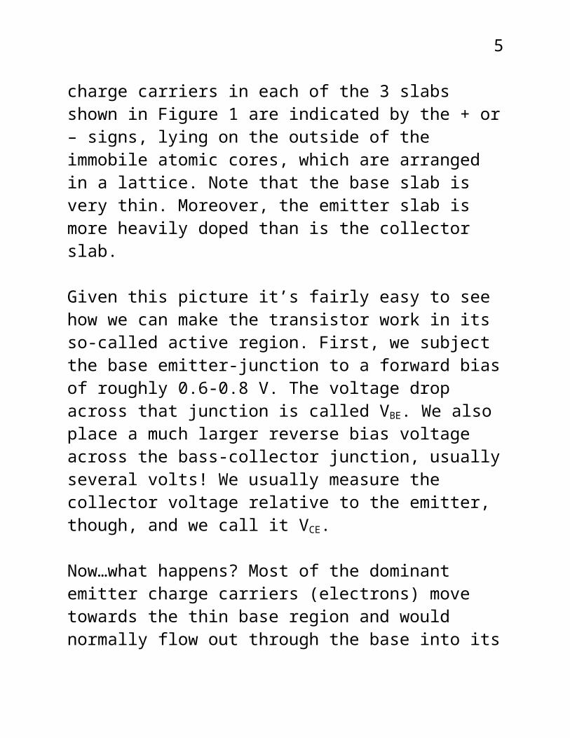
Transistors come in 2 flavors…npn and pnp. The makeup of an npn transistor is shown at left in Figure 1. It can be viewed simply as a pair of diodes connected back-to-back. The “block” of material making up the transistor is a 3-slab sandwich of silicon, each slab having been
doped with an impurity so that they have excess charge carriers of a particular type. For example, if we add a material that has one more valence electron than silicon’s four, like phosphorus, arsenic, or antimony (which are all in the same column on the periodic table…the one just to the right of silicon), we get a
Figure 1
3
semiconductor with more electrons free to move in the conduction band. This makes n-type silicon, whose dominant charge carriers are negative (-) electrons. Conversely, if we add boron, aluminum, gallium, or indium (once again, all from the same column in the periodic table, but one column to the left of silicon), this creates a semiconductor with a deficit of electrons (called holes) in the conduction band. This makes p-type silicon, whose dominant charge carriers are positive (+) holes (whew, this is getting into some ugly chemistry, isn't it?). The dominant mobile charge carriers in each of the 3 slabs shown in Figure 1 are indicated by the + or – signs, lying on the outside of the immobile atomic cores, which are arranged in a lattice. Note that the base slab is very thin. Moreover, the emitter slab is more heavily doped than is the collector slab.
Given this picture it’s fairly easy to see how we can make the transistor work in its so-called active region. First, we subject the base emitter-junction to a forward bias of roughly 0.6-0.8 V. The voltage drop across that junction is called VBE. We also place a much larger reverse bias voltage across the bass-collector junction, usually several volts! We usually measure the collector voltage relative to the emitter, though, and we call it VCE.
Now…what happens? Most of the dominant emitter charge carriers (electrons) move towards the thin base region and would normally flow out through the base into its external connection in the form of a base current IB. However, the big, bad collector, with its strong + voltage, VCE, is sitting very close to the emitter (because the base is quite thin) and it “gobbles up”, or collects, most of the emitter’s charge carriers being injected into the base
4
region. The charge carriers that flow out of the base are barely a trickle compared to the number of carriers that flow into and then out of the collector in the form of a collector current IC. Thus, IC is a little bit less than IE, the emitter current. Note that conventional current flow is opposite the direction of the flow of negative carriers that take place in npn transistors. For pnp transistors, direction of flow of the positive ‘holes’ is identical to that of conventional current.
The relationship between these 3 currents is …
and dividing by IE we get…
where α = Ic / IE
Thus…
Solving for IC…
(5.1)Typical values for α are about 0.95 – 0.995…most of the emitter current being swept up by the collector. Thus β ranges from about 20 – 200!
5
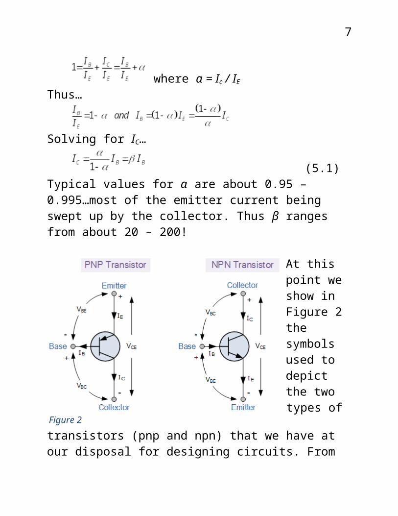
At this point we show in Figure 2 the symbols used to depict the two types of transistors (pnp and npn) that we have at our disposal for designing circuits.
From the previous discussion we can see that transistors can deliver a huge current gain β as seen from the perspective of the base. We’ll see how we can design transistor circuits that exploit this fact in spite of omitting more detail about many subtleties we’ve ignored.
First, a few simple rules to keep in mind before we start designing circuits:
1. Bias Polarity: The collector must be more positive than the base, which must be more positive than the emitter. Notice in Figure 2 that the symbols are arranged so that the largest possible bias voltage is always on top and decreases as you proceed to the bottom of the symbol. In many books, you’ll see the orientation of the symbols arranged willy-nilly, particularly in circuit diagrams containing more than one transistor. I have always found this to be terribly confusing. In my mind, current, like water, always flows downhill and the above symbol orientations are consistent with that mode of thought.
2. Junctions: The base-emitter and base-collector junctions act like diodes. Establishing normal transistor operation requires a forward
Figure 2
6
bias of voltage drop VBE on the order of 0.6-0.8 volts on the base-emitter junction, while requires a reverse bias on the order of several volts on the base-collector junction.
3. Maximum Ratings: There are maximum values for IC, IB and VCE, which should not be exceeded. See listings in table 2.1, p. 74, table 2.2, p. 196 and table 8.1, pps 501-502 of your primary reference, The Art of Electronics (AOE) or check the manufacturer’s handbook.
4. Current Amplification: IC = β IB in a transistor’s normal operating regime. However, there is a caveat… β is a mercurial parameter! A given transistor might have a β whose value is 100, while another transistor of exactly the same model and fabricated by the same manufacturer might have a β equal to 30! Designing a circuit whose desired output is dependent on the value of β yields a circuit designed by a fool. If a transistor fails in a circuit and you replace it, you do not want the output to change.
5.2 Transistor Operating Regions
There a three regions in which transistors normally operate:i. Active region - the transistor operates as an amplifier…IC = βIB as
described above.ii. Saturation – The transistor is “fully on” acting like a closed switch,
or a short circuit. Current freely flows from collector to emitter. IC = I (saturation). The collector voltage is typically about 0.2 V above the emitter voltage (for an npn transistor…the reverse for pnp). Thus, the base-collector junction is forward-biased as is the base-emitter voltage.
iii. Cut-off – The transistor is “fully off” acting like an open switch, or an open circuit. No current flows from collector to emitter. IC = 0. The collector voltage is typically the same as…or very close to…the collector power supply voltage, VCC.
First we’ll present some basic transistor circuits in which the transistor is operating in the active region.
7
A. The Emitter Follower
Shown in Figure 3 is an example of a circuit called the emitter follower. The output “follows” the input…less 1 diode voltage drop, i.e., VE ≈ VB – 0.6 volts. Thus, the output will sit at ground potential if the input drops below 0.6 V (if the bottom of the emitter resistor is grounded).
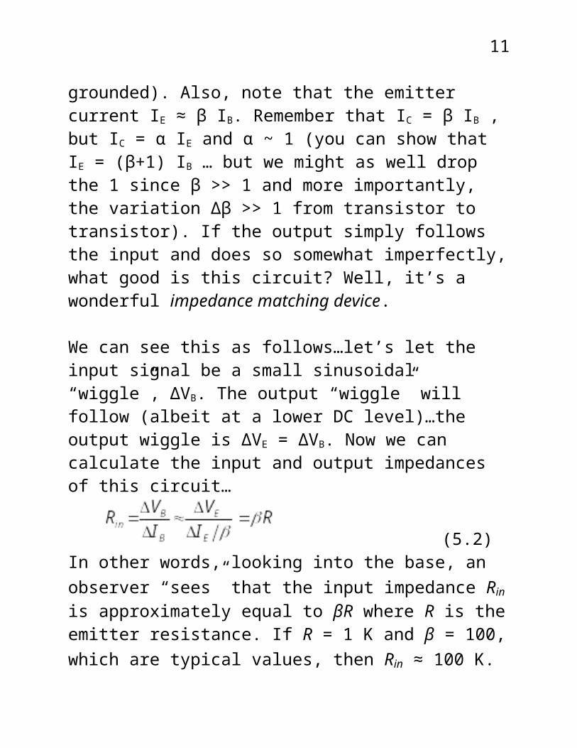
Also, note that the emitter current IE ≈ β IB. Remember that IC = β IB , but IC = α IE and α ~ 1 (you can show that IE = (β+1) IB … but we might as well drop the 1 since β >> 1 and more importantly, the variation Δβ >> 1 from transistor to transistor). If the output simply follows the input and does so somewhat imperfectly, what good is this circuit? Well, it’s a wonderful impedance matching device.
We can see this as follows…let’s let the input signal be a small sinusoidal “wiggle”, ΔVB. The output “wiggle” will follow (albeit at a lower DC level)…the output wiggle is ΔVE = ΔVB. Now we can calculate the input and output impedances of this circuit…
(5.2)In other words, looking into the base, an observer “sees” that the input impedance Rin is approximately equal to βR where R is the emitter resistance. If R = 1 K and β = 100, which are typical values, then Rin ≈ 100 K.
Figure 3
8
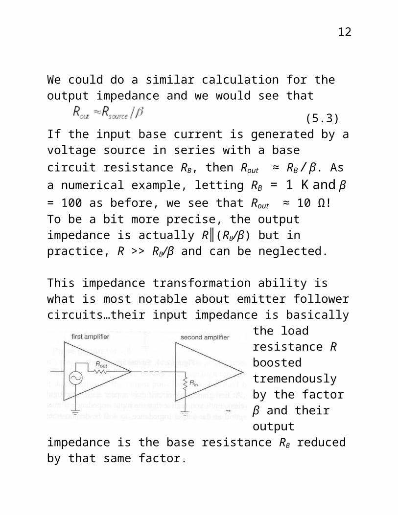
We could do a similar calculation for the output impedance and we would see that
(5.3)If the input base current is generated by a voltage source in series with a base circuit resistance RB, then Rout ≈ RB / β. As a numerical example, letting RB = 1 K and β = 100 as before, we see that Rout ≈ 10 Ω! To be a bit more precise, the output impedance is actually R║(RB/β) but in practice, R >> RB/β and can be neglected.
This impedance transformation ability is what is most notable about emitter follower circuits…their input impedance is basically the load resistance R boosted tremendously by the factor β and their output impedance is the base resistance RB
reduced by that same factor.Thus, if you are dealing with, say, a 2-stage amplifier (Figure 4) whose 1st stage output is a voltage, but whose
output impedance is fairly sizeable, say 1-10 K or so, then if you try to pass its output signal into a 2nd stage whose input impedance is comparable, it will act as a voltage divider and you’ll load down the signal you’re trying to pass on to the 2nd stage. Solution…insert an emitter follower between the two stages and you won’t load down the 1st stage signal.
Thus, emitter followers are typically used when the following
Figure 4
9
situations are encountered. You need…i. A low impedance signal source within a circuit or at its output.
ii. To convert a high impedance voltage reference, such as derived from a voltage divider, into a stiff voltage reference, i.e., one with low output impedance.
iii. To, in general, isolate a signal source from the loading effect of following stages.
There are caveats to pay attention to when using emitter followers.

10
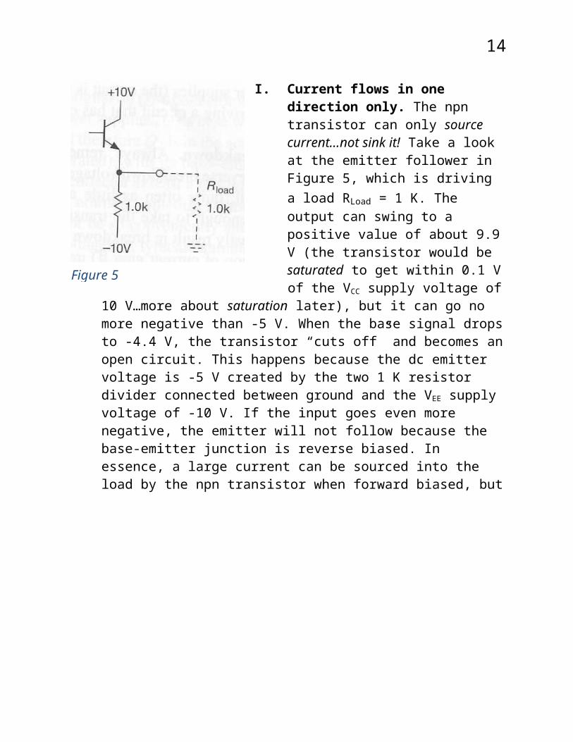
I. Current flows in one direction only. The npn transistor can only source current…not sink it! Take a look at the emitter follower in Figure 5, which is driving a load RLoad = 1 K. The output can swing to a positive value of about 9.9 V (the transistor would be saturated to get within 0.1 V of the VCC supply voltage of 10 V…more about saturation later), but it can go no more negative than -5 V. When the base signal drops to -4.4 V, the transistor “cuts off” and becomes an open circuit. This happens because the
dc emitter voltage is -5 V created by the two 1 K resistor divider connected between ground and the VEE supply voltage of -10 V. If the input goes even more negative, the emitter will not follow because the base-emitter
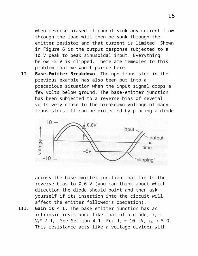
junction is reverse biased. In essence, a large current can be sourced into the load by the npn transistor when forward biased, but when reverse biased it cannot sink any…current flow through the load will then be sunk through the emitter resistor and that current is limited. Shown in Figure 6 is the output response subjected to a 10 V peak to peak sinusoidal input. Everything below -5 V is clipped. There are remedies to this problem that we won’t pursue here.
II. Base-Emitter Breakdown. The npn transistor in the previous example has also been put into a precarious situation when the input signal drops a few volts below ground. The base-emitter junction has been subjected to a reverse bias of several volts…very close to the breakdown voltage of many
Figure 5
Figure 6
11
transistors. It can be protected by placing a diode across the base-emitter junction that limits the reverse bias to 0.6 V (you can think about which direction the diode should point and then ask yourself if its insertion into the circuit will affect the emitter follower’s operation).
III. Gain is < 1. The base emitter junction has an intrinsic resistance like that of a diode, rE ≈ VT* / IC. See Section 4.1. For IC = 10 mA, rE ≈ 5 Ω. This resistance acts like a voltage divider with the load. Typical gains range from 0.95-0.99 and are dependent on the collector current. This value and its variation are in general not much of a concern.
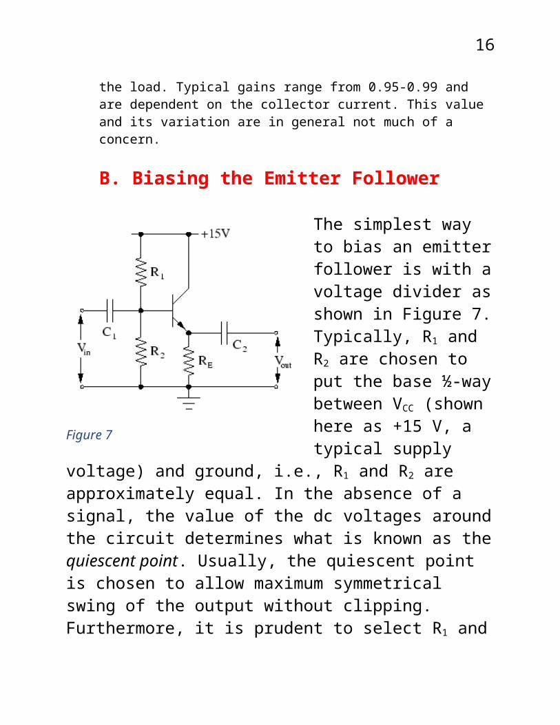
B. Biasing the Emitter Follower
The simplest way to bias an emitter follower is with a voltage divider as shown in Figure 7. Typically, R1 and R2 are chosen to put the base ½-way between VCC (shown here as +15 V, a typical supply voltage) and ground, i.e., R1 and R2 are approximately equal. In the absence of a signal, the value of the dc voltages around the circuit
determines what is known as the quiescent point. Usually, the quiescent point is chosen to allow maximum symmetrical swing of the output without clipping. Furthermore, it is prudent to select R1 and R2 so that the impedance their parallel combination presents to Vin is less than the impedance seen “looking into the transistor’s base, i.e., R1║R2 < β RE. Thus, variations in RE won’t affect the quiescent operating point very much, but you don’t
Figure 7
12
want to make R1║R2 too small. This would increase power dissipation and would wreck one of the emitter follower’s primary functions, namely, to present a high impedance to the signal source.
Example 5.1
Let’s make an ac-coupled emitter follower (Figure 7) for audio signals (20 Hz – 20 KHz). Also, set VCC = 15 V and quiescent current = 1 mA.
Step 1. Choose VE. For the largest possible symmetrical swing without clipping, VE = ½ VCC = 7.5 V. This brings up the reason why the output is ac-coupled via capacitor C2. The output will most likely drive a circuit whose quiescent input is different than 7.5 V. Moreover, resistance tolerances and variations in transistor β could lead to an output dc level a few 100 mV different than 7.5 V.
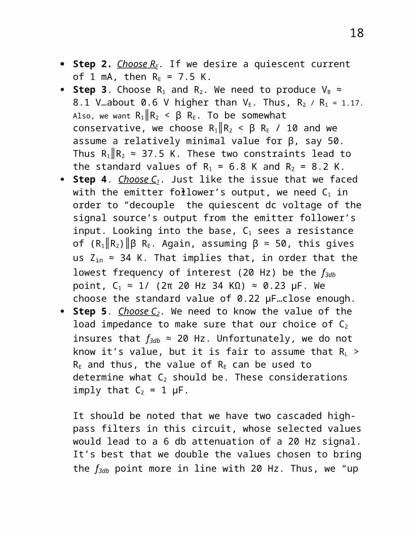
Step 2. Choose RE. If we desire a quiescent current of 1 mA, then RE = 7.5 K. Step 3. Choose R1 and R2. We need to produce VB ≈ 8.1 V…about 0.6 V
higher than VE. Thus, R2 / R1 = 1.17. Also, we want R1 R║ 2 < β RE. To be somewhat conservative, we choose R1 R║ 2 < β RE / 10 and we assume a relatively minimal value for β, say 50. Thus R1 R║ 2 ≈ 37.5 K. These two constraints lead to the standard values of R1 = 6.8 K and R2 = 8.2 K.
Step 4. Choose C1. Just like the issue that we faced with the emitter follower’s output, we need C1 in order to “decouple” the quiescent dc voltage of the signal source’s output from the emitter follower’s input. Looking into the base, C1 sees a resistance of (R1 R║ 2)║β RE. Again, assuming β ≈ 50, this gives us Zin ≈ 34 K. That implies that, in order that the lowest frequency of interest (20 Hz) be the f3db point, C1 ≈ 1/ (2π 20 Hz 34 KΩ) ≈ 0.23 μF. We choose the standard value of 0.22 μF…close enough.
Step 5. Choose C2. We need to know the value of the load impedance to make sure that our choice of C2 insures that f3db ≈ 20 Hz. Unfortunately, we do not know it’s value, but it is fair to assume that RL > RE and thus, the value of RE can be used to determine what C2 should be. These considerations imply that C2 = 1 μF.
13
It should be noted that we have two cascaded high-pass filters in this circuit, whose selected values would lead to a 6 db attenuation of a 20 Hz signal. It’s best that we double the values chosen to bring the f3db point more in line with 20 Hz. Thus, we “up the game a bit” picking C1 = 0.47 μF and C2 = 2.2 μF.
The emitter output impedance is approximately Zout ≈ RE ║[ZS║(R1║R2)/ β], where ZS is the impedance of the signal source. Assuming ZS = 10 K and β = 50, we obtain Zout ≈ 154 Ω. It should be noted that we’ve neglected rE, the intrinsic emitter resistance in these calculations. It’s usually small potatoes. Here, its value is VT*/1 mA ≈ 25 – 50 Ω, since VT* ranges between 25 – 50 mV. Furthermore, given the mercurial value of β and the fact that we know not either the source or load impedance, why push for accuracy?
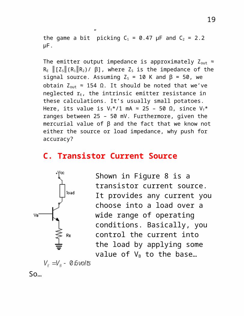
C. Transistor Current Source
Shown in Figure 8 is a transistor current source. It provides any current you choose into a load over a wide range of operating conditions. Basically, you control the current into the load by applying some value of VB to the base…
So…
But, since IC ≈ IE for large β…
independent of VC, as long as the transistor is not forced into saturation (VC ≥ VE + 0.2 volts) or cutoff (VC ≈ VCC).
Figure 8
14
This transistor configuration works as a current source because the collector is reverse-biased and therefore its output impedance is quite large. It works much better than simply attaching a voltage source to a relatively large resistor, but it’s not ideal. Collector impedances are on the order of mega-ohms, which, however, do show a relatively small variation with voltage. There are fixes, though, which are even better, but we leave them to a later discussion…or never, depending upon time.
D. Biasing the Transistor Current Source
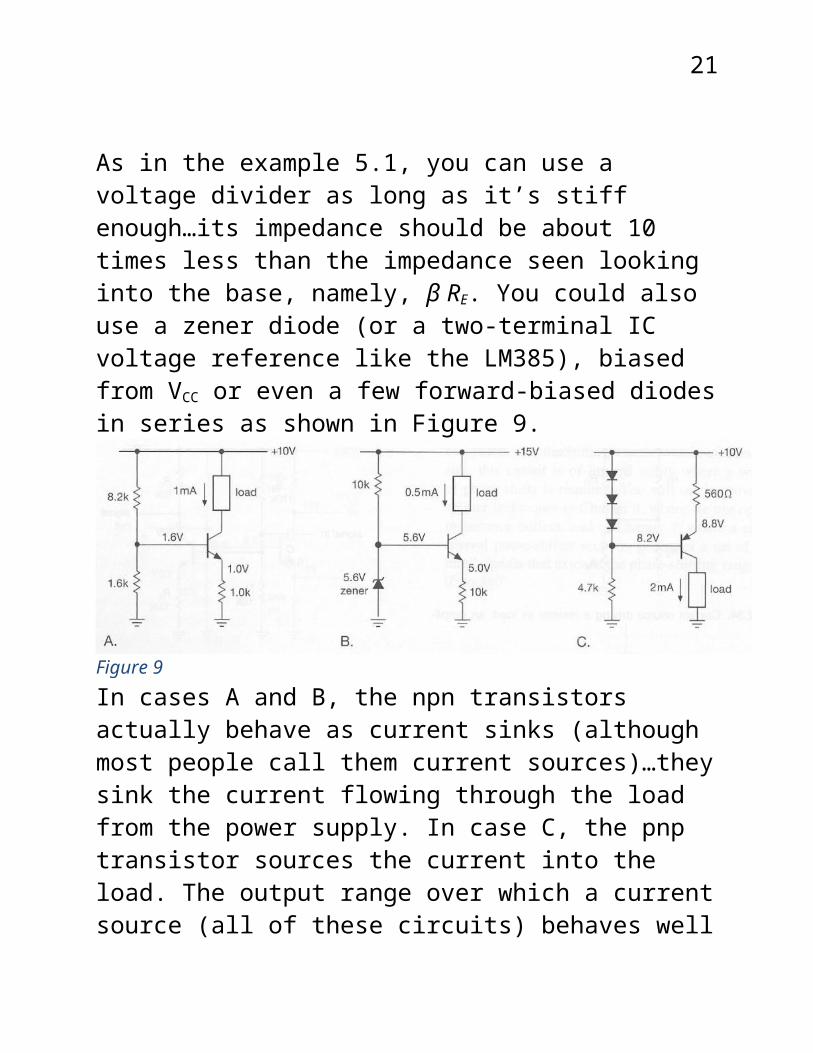
As in the example 5.1, you can use a voltage divider as long as it’s stiff enough…its impedance should be about 10 times less than the impedance seen looking into the base, namely, β RE. You could also use a zener diode (or a two-terminal IC voltage reference like the LM385), biased from VCC or even a few forward-biased diodes in series as shown in Figure 9.
In cases A and B, the npn transistors actually behave as current sinks (although most people call them current sources)…they sink the current flowing through the load from the power supply.
Figure 9
15
In case C, the pnp transistor sources the current into the load. The output range over which a current source (all of these circuits) behaves well is called compliance…set by the requirement that the transistor is not forced out of the active region. Thus, in A, VC can range from almost 10 volts down to about 1.1 – 1.2 volts. In B, it can only drop down to about 5.1 volts. In C, VC can range from ground up to about 8.6 volts.
The current source doesn’t have to have a fixed voltage VB. If the base is driven by a variable voltage source vin, the output current will vary proportionately and smoothly (as long as the transistor remains within compliance) as…iout = vin / RE. In fact, this property is the basis of the common emitter amplifier, which is capable of generating a large gain, as we’ll see in the next section.
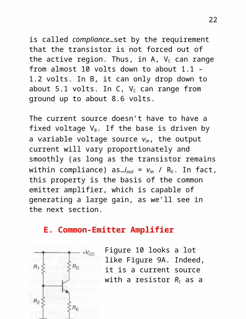
E. Common-Emitter Amplifier
Figure 10 looks a lot like Figure 9A. Indeed, it is a current source with a resistor RC as a load. The collector voltage is
VC = VCC – IC RC
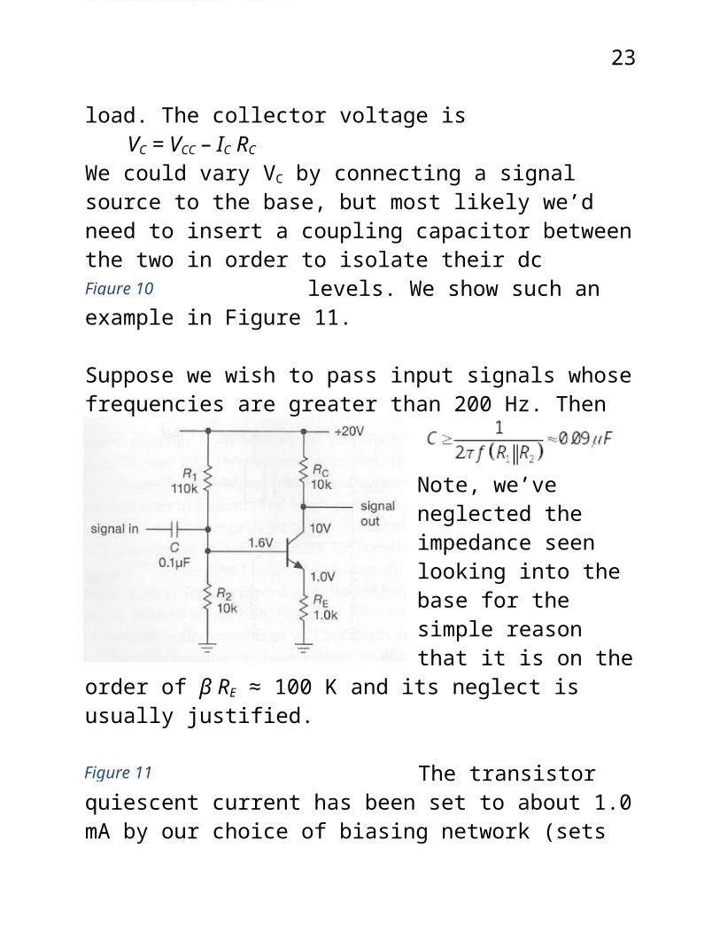
We could vary VC by connecting a signal source to the base, but most likely we’d need to insert a coupling capacitor between the two in order to isolate their dc levels. We show such an example in Figure 11.Figure 10
16
Suppose we wish to pass input signals whose frequencies are greater than 200 Hz. Then
Note, we’ve neglected the impedance seen looking into the base for the simple reason that it is on the order of β RE ≈ 100 K and its neglect is usually justified.
The transistor quiescent current has been set to about 1.0 mA by our choice of biasing network (sets VB = 1.6 volts) and the value of RE = 1.0 K. That current establishes VC = 10 volts, half-way between VCC and ground.
Now suppose we apply a base input “wiggle signal” vB, which leads to an equivalent emitter wiggle of vE = vB. This causes a wiggle in the emitter current iE = vE / RE and nearly the same wiggle in iC. Finally, this wiggle cause a wiggle in collector voltage
vC = -iC RC = -vB (RC / RE)Aha! We have a voltage amplifier whose gain is given by
vout / vin = - RC / RE (5.4)…in this case about -10. The minus sign means that a positive wiggle in the base generates a 10 times greater negative wiggle in the collector. This is called a common-emitter amplifier with emitter degeneration.
Figure 11
17
-----------------------------------------------------------------------------Problem. Estimate the input impedance and output impedance of this amplifier (include the effect of the emitter resistance RE in your estimate).Answer. You should get about 8K and 10K respectively.-----------------------------------------------------------------------------
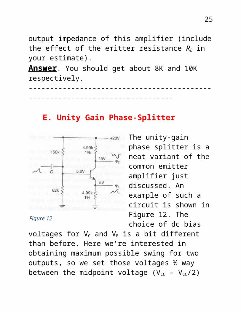
E. Unity Gain Phase-Splitter
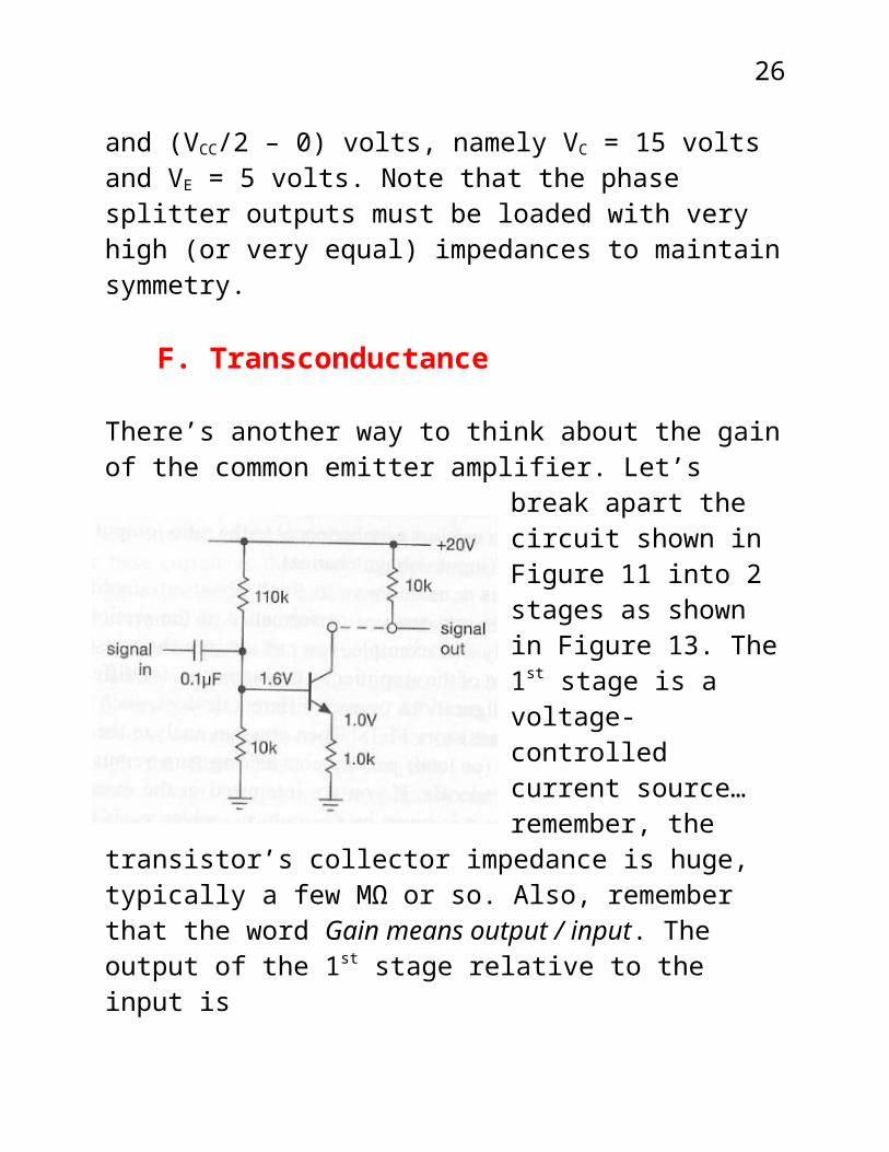
The unity-gain phase splitter is a neat variant of the common emitter amplifier just discussed. An example of such a circuit is shown in Figure 12. The choice of dc bias voltages for VC and VE is a bit different than before. Here we’re interested in obtaining maximum possible swing for two outputs, so we
set those voltages ½ way between the midpoint voltage (VCC – VCC/2) and (VCC/2 – 0) volts, namely VC = 15 volts and VE = 5 volts. Note that the phase splitter outputs must be loaded with very high (or very equal) impedances to maintain symmetry.
F. Transconductance
There’s another way to think about the gain of the common emitter amplifier. Let’s break apart the circuit shown in Figure 11 into 2 stages as shown in Figure 13. The 1st stage is a voltage-
Figure 12
18
controlled current source…remember, the transistor’s collector impedance is huge, typically a few MΩ or so. Also, remember that the word Gain means output / input. The output of the 1st
stage relative to the input is
Gain (gm) = ΔIout / ΔVin = iout / vin
(5.5)gm is called the transconductance, i.e., the transistor is acting as a voltage to current amplifier, whose gain in this circuit is -1 mA/V.
The 2nd stage of the circuit is simply the load resistor, RC, which converts the collector current into a voltage, vout. The voltage gain of the composite two stages is
GV = gm RC = (-1 mA/V) 10 K = -10.
You might be asking yourself, “What is the
point of all this?” First, once you know the transconductance of a circuit, you can then easily figure out what loads are going to throw the circuit out of compliance. Second, the overall voltage gain is trivial to calculate by multiplying the transconductance by the load impedance. Third, if you use an active load that is a current source, you can generate enormous voltage gains on the order of 10,000 or more. We’ll encounter such examples later on.
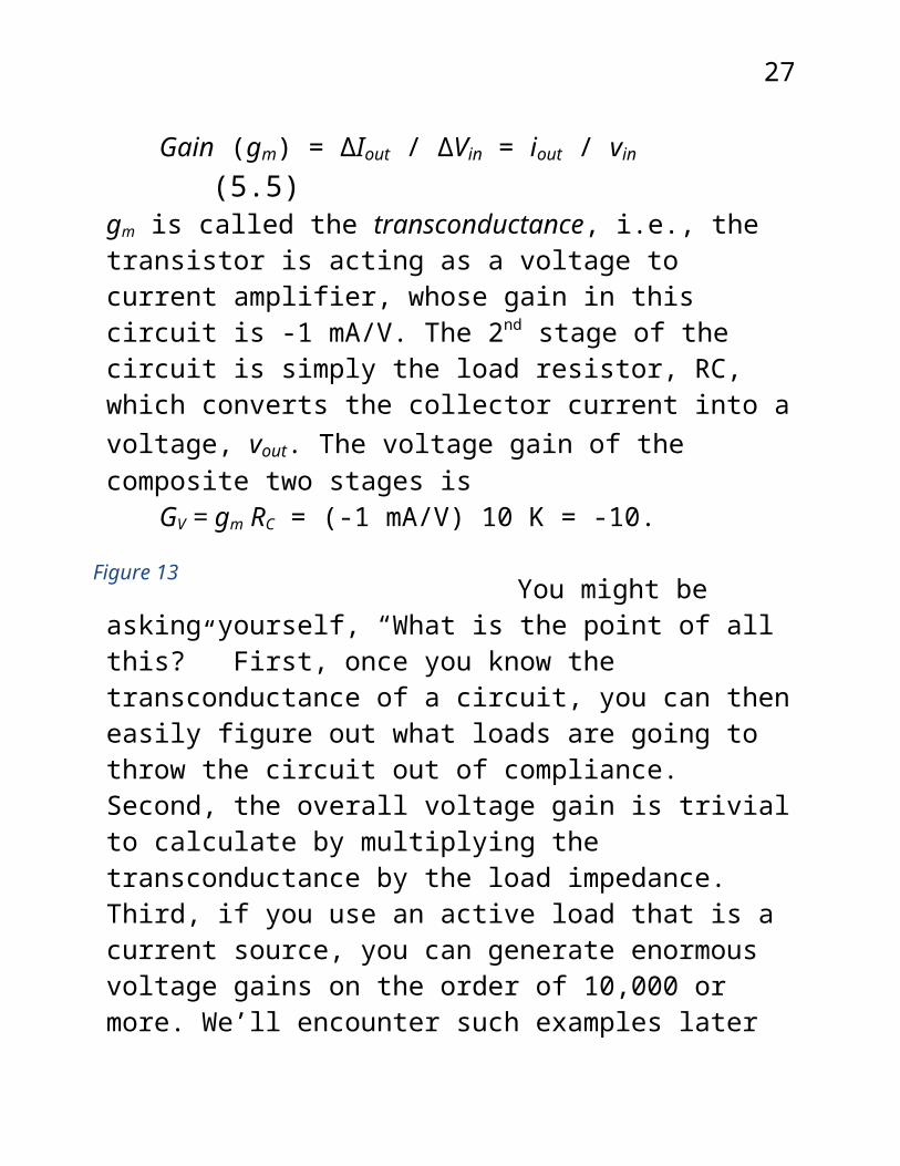
Figure 13
19
5.3 Saturation and Cutoff – Transistor Switch
As previously noted, ransistors have three basic modes of operation; active, saturation and cutoff. Our previous discussion gave examples of transistors operating in the active mode, but here we show how the transistor can be operated as a simple switch, working between saturation and cutoff.
Figure 14 shows a typical application in which a transistor operates as a switch whose purpose is to turn off and on an LED (light emitting diode). You can see in the figure that the transistor behavior can be approximately represented as a simple open-closed switch. Red LED’s will light up typically when a few milliamps is driven
through them. They’ll barely glow when driven by 1 mA but the light they emit will knock your eye out if driven by 30 mA or thereabouts. The switch is closed by applying 5 volts to the input base resistor R1 and opened by applying 0 volts. Note that when the switch is turned on, approximately IB ≈ 5 mA. If β were equal to 100 (as it likely would be if the transistor was operating in the active region), then IE ≈ IC = 0.5 A. The voltage drop across the 100 Ω collector resistor R2 would then be 50 V! The voltage drop across red LED’s, when turned on is typically around 2 V. Thus, the collector voltage VC would be about – 43 V! Clearly, this cannot happen since the transistor is basically a
Figure 14
20
short circuit to ground and VC can never drop below about 0.2…the voltage drop across a saturated transistor. Obviously β ≠ 100. In fact, as a transistor is forced into saturation by applying ever larger base currents, β drops precipitously. In this example, the collector current reaches a maximum when the transistor is saturated. The voltage across the current limiting collector resistor will be about 2.8 V (2 V across the diode and 0.2 V across the transistor). Thus, ICmax ≈ 2.8 V/100 Ω = 28 mA. β has been forced down to a value of 28/5 = 5.6! Further increases in IB would serve no purpose other than to simply force β down even further without changing IC one iota (or the brightness of the LED).
The npn transistor in the above circuit is operating as a low-side switch…the transistor is connected to the low voltage side (in the above case, gnd) of power supply. Note, that the transistor is turned on (conducting) when the input control voltage is “high” or +5 V and the transistor is turned off when the input control voltage is “low” or 0 V.
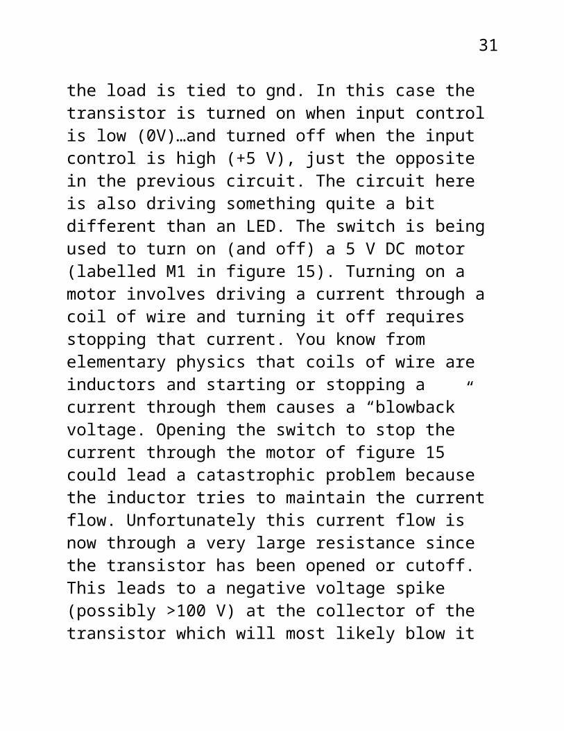
We can use a pnp transistor to make a high-side switch. We show such a switch in figure 15. The emitter of the transistor is tied to the high voltage side of the supply and the load is tied to gnd. In this case the transistor is turned on when input control is low (0V)…and turned off when the input control is high (+5 V), just the opposite in the previous circuit. The circuit here is also driving something quite a bit different than an LED. The switch is being used to turn on (and off) a 5 V DC motor (labelled M1 in figure 15). Turning on a motor involves driving a current through a coil of wire and turning it off requires stopping that current. You know from elementary physics that coils of wire
21
are inductors and starting or stopping a current through them causes a “blowback” voltage. Opening the switch to stop the current through the motor of figure 15 could lead a catastrophic
problem because the inductor tries to maintain the current flow. Unfortunately this current flow is now through a very large resistance since the transistor has been opened or cutoff. This leads to a negative voltage spike (possibly >100 V) at the collector
of the transistor which will most likely blow it to smithereens. The solution is to place a diode “clamp” across the motor’s terminals, which allows the current to keep flowing in a loop for a while through the motor and the diode. The voltage at the transistor collector is “clamped” one diode voltage drop below ground thus rescuing it from doom. Diodes used for this purpose are called flyback diodes. They usually have breakdown voltage ratings of about 20 V but tremendous power ratings enabling them to handle large currents typically associated with motors.
5.4 Transistor Switches in Digital LogicTransistors can be combined to create all our fundamental digital logic: AND, OR, and NOT.
22
(Note: These days MOSFETS are more likely to be used to create logic gates than BJTs. MOSFETs are more power-efficient, which makes them the better choice.)
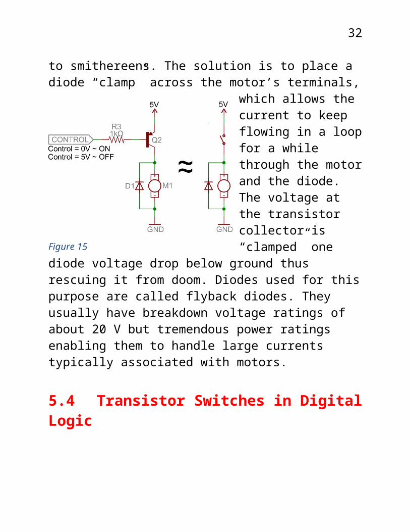
InverterFigure 16 shows a transistor circuit that implements an inverter, or NOT gate:
Here a high voltage (say, +5V, which we call a logical 1) into the base will turn the transistor on, which will effectively connect the collector to the emitter. Since the emitter is connected directly to ground, the collector will be as well…almost (it will be slightly higher, somewhere around VCE(sat) ~ 0.05-0.2V). In other words, the output will be ~0V, or logical 0. On the other hand, if the input is low
(logical 0), the transistor looks like an open circuit, and the output is pulled up to VCC (or logical 1, assuming VCC = +5V). In logic, we would say if the input is Y, the output is NOT Y, or
.
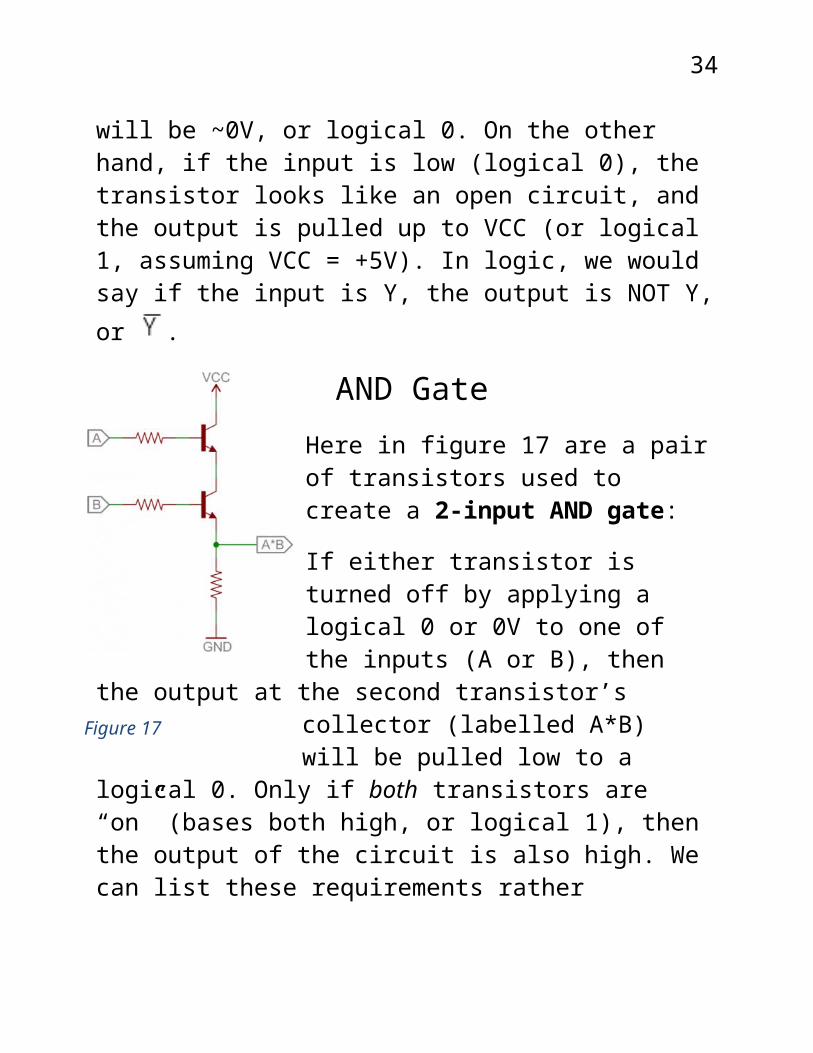
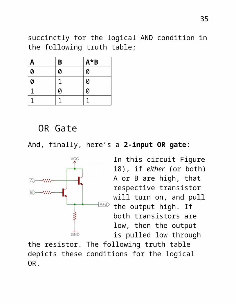
AND GateHere in figure 17 are a pair of transistors used to create a 2-input AND gate:
Figure 16
23
If either transistor is turned off by applying a logical 0 or 0V to one of the inputs (A or B), then the output at the second transistor’s collector (labelled A*B) will be pulled low to a logical 0. Only if both transistors are “on” (bases both high, or logical 1), then the output of the circuit is also high. We can list these requirements rather succinctly for the logical AND
condition in the following truth table;
A B A*B0 0 00 1 01 0 01 1 1
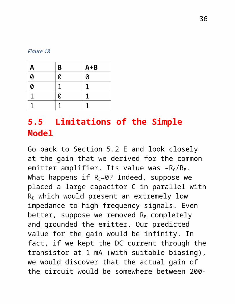
OR GateAnd, finally, here’s a 2-input OR gate:
In this circuit Figure 18), if either (or both) A or B are high, that respective transistor will turn on, and pull the output high. If both transistors are low, then the output is pulled low through the resistor. The following truth table depicts these conditions for the logical OR.
Figure 17
Figure 18
24
A B A+B0 0 00 1 11 0 11 1 1
5.5 Limitations of the Simple ModelGo back to Section 5.2 E and look closely at the gain that we derived for the common emitter amplifier. Its value was –RC/RE. What happens if RE→0? Indeed, suppose we placed a large capacitor C in parallel with RE which would present an extremely low impedance to high frequency signals. Even better, suppose we removed RE completely and grounded the emitter. Our predicted value for the gain would be infinity. In fact, if we kept the DC current through the transistor at 1 mA (with suitable biasing), we would discover that the actual gain of the circuit would be somewhere between 200-400. Moreover, the actual value of the gain would be a bit “mercurial”. Indeed, if you changed transistors in the circuit, you’d obtain a value for the gain significantly different than the one you had with the old transistor. As additional insults, the amplifier would become significantly non-linear…the output would be a distorted image of the input and the gain would be highly temperature dependent. Can you guess why?
The answer to this question was hinted at in the discussion of the emitter follower “caveats” in section 5.2A. The transistor conducts when the base-emitter junction is forward biased. It is essentially a junction diode and its behavior when forward biased is well-described by the Ebers-Moll equation, which is
25
essentially the equation presented in section 4.1 that relates the current through a forward-biased diode as a function of the voltage across the junction. The I vs V curve for an actual diode and the idealized equation that describes it was shown in figure 2. The slope of that curve at any forward biased voltage is the diode’s transconductance, or the inverse of its resistance. Thus, what we are getting at here is the base-emitter junction, being a forward-biased diode, exhibits an intrinsic resistance rE that is quite small. Its value is dependent on the current through it, it is highly temperature dependent and it varies from one transistor to another. Clearly, the gain that we derived for the common emitter amplifier should have been –RC/(RE + rE). The value of RE swamps out rE in the circuits we’ve discussed so far, but look out when RE→0!
5.6 Subleties – Ebers-Moll ModelSo far we’ve used a simple model of the BJT to design four types of circuits: (i) emitter follower (ii) current source (iii) common emitter amplifier and (iv) switches. We’ve simply used the relation IC = βIB, where we have basically thought of the input to the transistor as a current-controlled device operating essentially as a current amplifier. Most circuit designers think this way. After all, the input impedance to a transistor devoid of a resistor in the emitter circuit is quite low and therefore ought to be controlled by an input current rather than a voltage. However, many circuits such as differential amplifiers (which are the input stage to some operational amplifiers, or op amps), logarithmic converters, temperature compensation and many others require you to think of the transistor as a
26
transconductance device…output collector current is controlled by an input base-emitter voltage.
So, instead of thinking of the transistor as a current amplifier as depicted by rule 4 in section 5.1 (essentially, IC = βIB), let’s write down the equation for the relationship between IC and VBE. It is…
(5.6a)VT ~ 25 mV at room temperature. Furthermore, we note that the reverse-bias leakage current IS is a strong function of temperature T and is typically 1 pA – 1 fA.
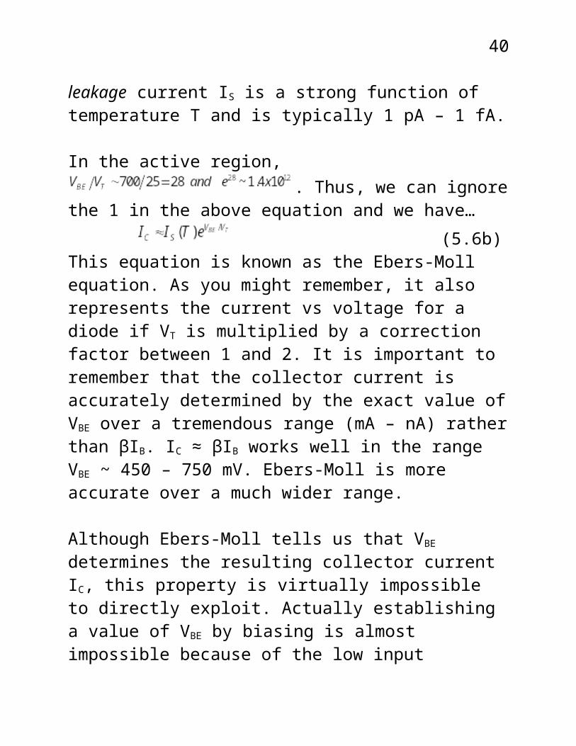
In the active region, . Thus, we can ignore the 1 in the above equation and we have…
(5.6b)This equation is known as the Ebers-Moll equation. As you might remember, it also represents the current vs voltage for a diode if VT is multiplied by a correction factor between 1 and 2. It is important to remember that the collector current is accurately determined by the exact value of VBE over a tremendous range (mA – nA) rather than βIB. IC ≈ βIB works well in the range VBE ~ 450 – 750 mV. Ebers-Moll is more accurate over a much wider range.
Although Ebers-Moll tells us that VBE determines the resulting collector current IC, this property is virtually impossible to directly exploit. Actually establishing a value of VBE by biasing is almost impossible because of the low input resistance of the transistor and the fact that the actual value of VBE is temperature dependent.
27
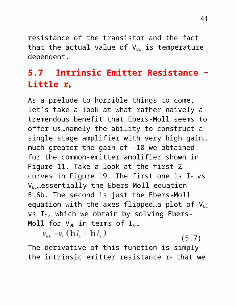
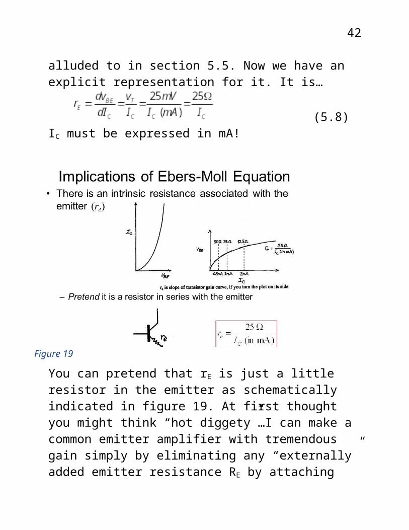
5.7 Intrinsic Emitter Resistance − Little rE As a prelude to horrible things to come, let’s take a look at what rather naively a tremendous benefit that Ebers-Moll seems to offer us…namely the ability to construct a single stage amplifier with very high gain…much greater the gain of -10 we obtained for the common-emitter amplifier shown in Figure 11. Take a look at the first 2 curves in Figure 19. The first one is IC vs VBE…essentially the Ebers-Moll equation 5.6b. The second is just the Ebers-Moll equation with the axes flipped…a plot of VBE vs IC, which we obtain by solving Ebers-Moll for VBE in terms of IC…
(5.7)The derivative of this function is simply the intrinsic emitter resistance rE that we alluded to in section 5.5. Now we have an explicit representation for it. It is…
(5.8)IC must be expressed in mA!

28
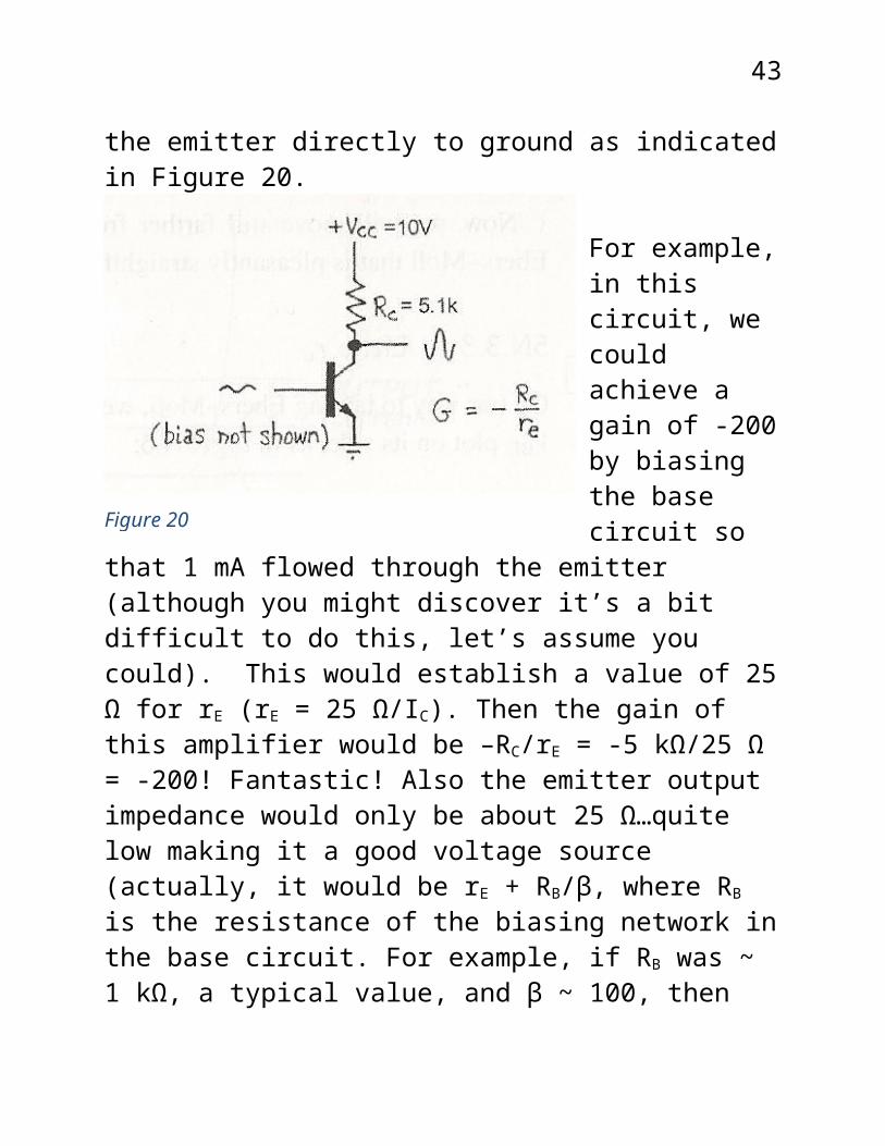
You can pretend that rE is just a little resistor in the emitter as schematically indicated in figure 19. At first thought you might think “hot diggety”…I can make a common emitter amplifier with tremendous gain simply by eliminating any “externally” added emitter resistance RE by attaching the emitter directly to ground as indicated in Figure 20.
For example, in this circuit, we could achieve a gain of -200 by biasing the base circuit so that 1 mA flowed
Figure 19
Figure 20
29
through the emitter (although you might discover it’s a bit difficult to do this, let’s assume you could). This would establish a value of 25 Ω for rE (rE = 25 Ω/IC). Then the gain of this amplifier would be –RC/rE = -5 kΩ/25 Ω = -200! Fantastic! Also the emitter output impedance would only be about 25 Ω…quite low making it a good voltage source (actually, it would be rE + RB/β, where RB is the resistance of the biasing network in the base circuit. For example, if RB was ~ 1 kΩ, a typical value, and β ~ 100, then RB/β ~ 10 Ω, making a total of 35 Ω, still quite low).
Unfortunately, the above circuit is horrible…it suffers numerous afflictions associated with rE…which it turns out is highly variable.
5.7 Distortion
30
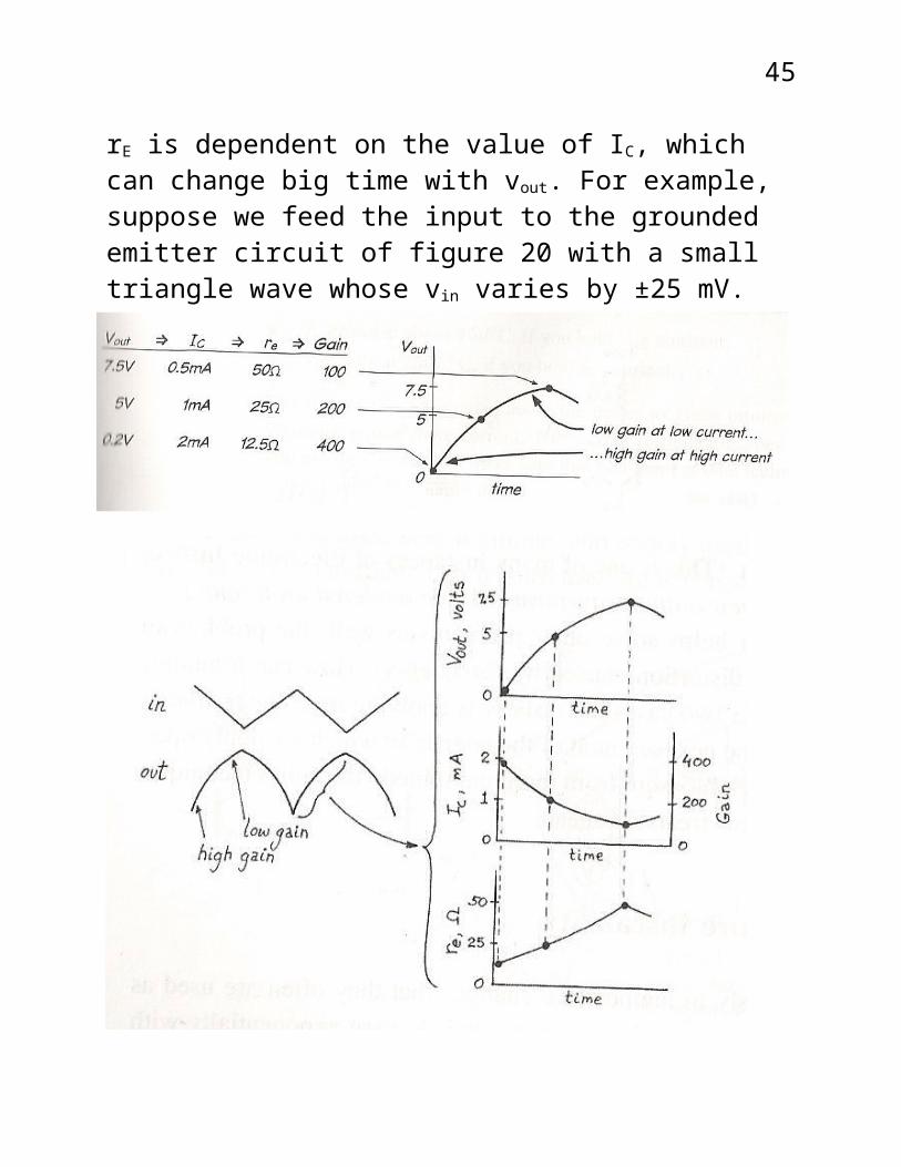
rE is dependent on the value of IC, which can change big time with vout. For example, suppose we feed the input to the grounded emitter circuit of figure 20 with a small triangle wave whose vin varies by ±25 mV. Since the gain of the amplifier is -200, vout will vary by ± 5 V…or so you might think. However, a change in Vout that big will also cause IC and therefore the gain to also change a lot. Figure 21 illustrates this problem in which we show how the gain varies in response to the input triangle wave.The effect of this variation should be obvious…it leads to a rather severe type of output signal distortion the author of your text has called “barn-roof” distortion…the output signal looks like a Vermont barn roof shown in Figure 22), which is an actual scope trace of input and output (the scope gain has been set to 100 x that of the output).
Figure 22
You can’t get rid of this variation in rE, but you can pretty much eliminate its effects. Just add an emitter resistor whose value swamps it out (already did this in the circuit of Figure 11). The result we obtain for the circuit here is shown in Figure 23. rE still varies as much as it did before if the input signal causes the
31
output to vary by the same amount. However, the variation is swamped by the much larger RE in the denominator of the gain factor. The variation is now only ±4%.
Basically what the resistor RE adds to the circuit is something called negative feedback…a truly remarkable tool to have in
one’s circuit design repertoire. Negative feedback can be thought of in the
following way: if somebody does something bad to you…you
32
act in such a way as to minimize the effect of their action. Positive feedback is the opposite. You might think of it as: if somebody does something good to you…you act to maximize its effect. Negative feedback in electronic circuits provides stability…positive feedback provides chaos (which, believe it not is sometimes desirable…such as designing oscillators).
We can easily see how the addition of RE provides negative feedback…if the input rises, so will the emitter voltage VE, which “fights back” on the forward bias of the base-emitter voltage, i.e., it minimizes the increase in VBE that would occur otherwise. Note, we have gained stability, but that comes with the price of lower gain…you can’t have your cake and eat too!
5.8 Temperature Instability and the Early Effect
If you take a look at the position of the temperature T in the Ebers-Moll equation, you would think that as the temperature of a transistor goes up, its output current IC would drop, which is contrary to both common sense and experience. Indeed, it does go up…sometimes catastrophically in a poorly designed circuit. The problem is IS(T), the reverse-bias saturation current in the Ebers-Moll equation…it increases rapidly with temperature…overwhelming the reducing effect of T in the exponent. The upshot can be expressed as two rules…
IC grows about 9% / oC, with VBE held constant…it doubles for an 8 oC rise.
VBE falls at 2 mV / oC…it is roughly proportional to 1/Tabs
The high gain circuit devoid of an RE feedback resistor pictured in Figure 20 is virtually useless. An 8 oC rise in temperature with
33
the collector biased at ½ the supply voltage will drive the transistor into saturation!
There is another effect not caused directly by temperature that can also create instability problems in a poorly designed circuit. It’s called the Early effect. VBE (at constant IC) varies slightly with VCE. This effect is caused by a change in the effective width of the transistor base region as VCE changes. It is given approximately by…
ΔVBE = - η ΔVCE where η ~ 10-4 – 10-5 (5.9)This is often expressed as a linear increase of collector current with increasing collector voltage when VBE is held constant. It is expressed as…
(5.10)where VA is known as the Early voltage and is typically 50 – 500 V. It is shown graphically in Figure 24. A low Early voltage leads to steeper curves as shown in the graph and this translates to lower collector resistance. Thus, the collector of the transistor doesn’t act as a good current source. This can have a deleterious effect on transistors driving moderately high impedances or on current mirror circuits, which we’ll discuss later on.
34
Figure 24
5.9 Temperature Stability and High Gain
Signal distortion and variation of gain can be greatly minimized by applying negative feedback. We’ve already demonstrated this with the addition of RE in the circuit of Figure 23. Also, negative feedback almost completely renders the effects of temperature
variation inconsequential. However, this benefit came at the expense of high gain. But could we circumvent this cost so that we could have our cake and eat it, too? Unlike with cake, it’s
possible with electronic circuits. The trick is to include RE as in the low gain amplifier of Figure 23, but then to bypass it with a
Figure 25a
35
capacitor to make it disappear in a desired signal frequency range. This bypass remedy is illustrated in Figure 25a.
The gain of this circuit at very low frequencies is -10. The higher frequency AC gain assuming 0 impedance for the capacitor would be –RC / rE. If the circuit were biased such that IC ~ 1.1 mA, the quiescent DC collector voltage VC would be VCC / 2 = 7.5 V and rE would be 25 mV/1.1 mA ~ 23 Ω. Thus, the high frequency AC gain would be about -300! The gain indicated in the scope trace is ‘only’ 235…that’s because the circuit was actually biased with IC ~ 0.86 mA, but you get the picture.
There is another way to achieve large gain
Figure 25b
Question:Assume the circuit in Figure 25a is biased such that rE~23 Ω. What is the value of the corner frequency for this circuit?
36
and yet stabilize it fairly well against temperature induced change. Use DC feedback to stabilize the quiescent point. You take the bias voltage from the collector rather than from the supply VCC. This technique is illustrated in Figure 26. The base voltage VB sits 1 diode drop above ground or ~ 0.6-0.7 V. The 6.8k and 68k resistors form a 10:1 divider and so the collector voltage must be must sit at (1 + 10) diode drops above ground or VC ~ 11 VBE ~ 7 V. The collector quiescent voltage is about ½-way between VCC and ground, generating a collector current of a little less than 1 mA. Any tendency for the transistor to be driven into saturation caused by a rise in temperature is stabilized, since the decreasing collector voltage will reduce VBE. The collector quiescent point might drift a volt or so, but in many cases this is acceptable if really high gain is asked for from a single stage.
There is a problem with this circuit though…the feedback acts to reduce its input and output impedances. The input signal sees the value of R1 effectively reduced by the gain of the amplifier…down to perhaps 200 Ω or so…potentially a real problem particularly if the output impedance of the signal source is non-negligible. Understanding this will require a more detailed presentation of feedback, which we’ll cover in a later lecture. For now, let’s just say that there are ways around this ‘impedance lowering effect’ and leave it at that.
5.10 Current Mirrors
Your text doesn’t introduce these incredibly slick circuits since almost no one designs and builds them, although someone must
37
since they are ubiquitous in IC’s. Indeed, someday you might get ‘backed up against a wall’ where you are forced to design a specialized IC yourself in which a current mirror might well be one of its components (of course, you’d ‘farm out’ your design to be manufactured by some company). Thus, your text does discuss them in quite some detail in Section 5S.2, Transistors II.
We show a schematic of a current mirror in Figure 27. Why devise such a circuit anyway since it’s easy to make current
sources many other ways? Mirrors are used to link currents in a circuit…matching one to another…or, indeed, making one current some multiple of the other. You can see how the mirror works by examining Figure 28. Notice that Q1’s collector and base are connected directly together. Thus, right off the git-go you can see that both the
Figure 27
38
collector and base will be roughly 1 diode drop above ground and that the current IPGM will be about 1 mA in this case. Since VBE2 = VBE1, IOUT = IPGM. This is true no matter what the value of the RLOAD is in Figure 27 (within limits). You can program the current as you like by simply adjusting RPGM appropriately.The direct connection between collector and base is another example of negative feedback. If more current flows through Q1, VC1 will drop thus decreasing the current through Q1…and the reverse is true. Thus, VBE1 will stabilize at a value of IC1 that generates a VBE1 consistent with that IC1.
A real plus for this circuit is its ability to operate from “rail to rail” (electronic jargon for “from one supply to the other”). In other words, it will work really well almost from saturation to cutoff…the current mirror has a really wide “compliance”, which explains its use in OP AMPS (another reason is that IC’s use transistors instead of resistors whenever possible). Several complications arise in current mirrors. First, if the temperatures of Q1 and Q2 diverge, 1:1 mirroring fails. There is an easy solution to this problem: put the two transistors close together in an IC (in fact, trying to build a mirror with two separate, discrete transistors wouldn’t win you any prizes). There are many options…for example, Analog Devices offers several such as the npn dual matched pair MAT01AHZ or the npn quad matched pair MAT14ARZ. VBE still changes with rising T but the feedback in in Q1 will lower its value of VBE and therefore that of Q2 which requires the identical amount of lowering since its temperature rises by the same amount as that of Q1.
39
Second…the Early effect is a bit of a problem for current mirrors…even in matched pair IC’s depending on the load that Q2 drives. Remember that the Early effect causes a change in VBE if VCE changes which will happen when Q2 drives a resistance load. Your text goes into excruciating detail to estimate the magnitude of the Early effect, which we will not bother with here. The parameter VA (the Early voltage discussed in Section 5.8) tells you whether or not you might have a problem. The larger VA is, the higher the collector impedance of the transistor. The higher the collector impedance, the better it can drive a resistive load without large changes in VCE…which minimizes the Early effect. So, simply use transistors with large VA’s. However, manufacturers do not list Early voltages in their specifications! If they happen to show IC vs VCE curves, you can directly estimate VA and even better,
the collector impedance of the transistor. If they don’t, they simply tell you to measure it yourself! Lovely! There is a better solution…the Wilson current mirror (Figure 29), which uses something in one of the legs called the cascode configuration.
An approximate analysis shows how the Wilson current mirror works and why its mirroring error should be very low. Transistors Q1 and Q2 in Figure 29 are a matched
pair sharing the same emitter and base potentials and therefore have IC1 = IC2 and IB1 = IB2. This is a simple two-transistor current
40
mirror with IE3 as its input and IC1 as its output. When a current Iin is applied to the input node (the connection between the base of Q3 and collector of Q1), the voltage from that node to ground begins to increase. As it exceeds the voltage required to bias the emitter-base junction of Q3, Q3 acts as an emitter follower and the base voltage of Q1 and Q2 begins to rise. As this base voltage increases, current begins to flow in the collector of Q1. All increases in voltage and current stop when the sum of the collector current of Q1 and base current of Q3 exactly balance Iin. Under this condition all three transistors have nearly equal collector currents and therefore approximately equal base currents. Let IB = IB1 = IB2 ≈ IB3. Then the collector current of Q1 is Iin - IB; the collector current of Q2 is exactly equal to that of Q1 so the emitter current of Q3 is IE3 = IC2 + 2IB. The collector current of Q3 is its emitter current minus the base current so Iout = Iin + IB - IB = Iin. In this approximation, the mirroring error is zero.
The virtue of this circuit is that Q3 doesn’t determine in any way the value of the output current. It merely passes that current to the load from Q2. Q2 is protected from the Early effect since its collector voltage IC2 does not change regardless of the value of the load. Therefore, Q1 is protected also since its base voltage IB1 must equal IB2. This design is the standard form for mirrors inside OP AMPS, such as the LF411. The program current is usually not set by a collector resistor RPGM, whose value is temperature dependent thus defeating the purpose of generating an ‘invariable’ current. Instead, it is usually programed by (you guessed it) another transistor as discussed in your text…but we’ll quit here.
41
5.11 Differential (Difference) Amplifier
The differential amplifier does what its name implies…it amplifies the difference between two input signals and ignores their absolute levels…only the difference matters. They are commonly used when a signal is transferred over a long distance via some “double conductor” cable such as: a twisted pair, Ethernet, coax or audio. One conductor might simply connect the ground of the signal source to the ground of the receiver while the other conductor carries the signal of interest. If the long cable picks up unwanted electrical noise from the environment…that noise is usually picked up by both conductors more or less equally. Audio signals, for example, are commonly afflicted with 60 Hz noise, which can cause an unwanted hum in the audio output. This noise is usually common mode…it afflicts the audio ground as well as the audio signal. Hence the task of difference amplifier is to reject that common mode noise and amplify the difference signal carried by the two conductors. In many cases, the common mode noise might swamp the signal by a factor of ten or more, but if the common mode rejection ratio (CMRR) is greater than this, the signal of interest is easily retrieved…almost magically.
Difference amplifiers are used universally as the input stage of operational amplifiers, which we’ll cover in a later lecture.
42
A typical differential amplifier (also called a long-tailed pair) is shown in Figure 30. You’ll actually build it in the lab. You’ll use an IC transistor array such as the CA3096 in order to achieve good matching (the array contains two pnp and 3 npn
transistors). Before analyzing how it
performs its task of amplifying a difference between two inputs and rejecting their common mode, we need to establish the DC quiescent operating conditions.
Quiescent PointsIf we tie the two bases to ground, then the voltage at point A in Figure 31 should be ~ -1 V. That means that the current through Rtail (the 10 k resistor that makes up the tail of the two emitters)
is ~ 1.5 mA (no need to be anal about accuracy). Since the two inputs are grounded, by symmetry, 0.75 mA flows through each collector. Thus, Vout DC is 7.5 V. Note, it is centered essentially between +VCC and ground…not between ±VCC.
This is because the output can swing essentially between +VCC and ground…not between ±VCC. The bottom of the possible voltage swing is determined by VA and that voltage cannot
Figure 30
Figure 31
43
change very much. Hence, our reason for the choice of biasing that places Vout DC at ~7.5 V…at the midpoint of the possible swing range.
Differential GainAssume that a pure difference signal Vin is presented to inputs A and B. What we mean by that is when the voltage at A is +Vin/2, the voltage at B will be –Vin/2. For example, it could be a small sine wave “wiggle” presented to A and another sine wave equal in frequency and amplitude, but shifted 180 O in phase, presented to B. Such a pair of signals could be derived from the common emitter amplifier shown in Figure 10 with RE = RC (such a circuit is known as a phase splitter and is discussed in Transistors I, 4W.2 of your text). You should see that VA in Figure 31 does not change. This lack of change occurs because the transistor that conducts a little more in response to the positive-going wiggle produces an increase in its emitter current of ΔIE ~ ΔIC while the other transistor that conducts less in response to its ‘equal but opposite’ negative-going wiggle produces an equal reduction in its emitter current leaving the
current through RTAIL the same as it was…2 IC,
Figure 32
44
where IC is the DC bias current that flows through each collector.
Thus you can treat the right side transistor (the one from which the output is derived) as the familiar common emitter amplifier with its emitter tied to the fixed voltage VA as shown in Figure 32.
Don’t make the mistake (as your text warns) of guessing that the gain is G = RC / (rE + RE) (forget about the – sign since we haven’t defined what we mean by + and – between the two inputs). That’s because the full difference voltage Vin defines the gain of the circuit not just the Vin/2 applied to each input. Vin/2 does produce the collector wiggle ΔIC seen in each transistor. The differential gain is
(5.11)Thus, the differential gain is halved from what Figure 32 might lead you to mistakenly conclude.
Common Mode GainIn this case assume a pure common mode signal: this can be generated by tying the two inputs together and applying the same identical sine wave wiggle to each of the inputs. VA is no longer fixed. It will rise and fall since each transistor conducts more (or less) in concert. This common mode amplifier will have a much smaller gain since RTAIL is relevant… and it is big!
Another factor of 2 appears in the calculation of the common mode gain because of the fact that not only is the “output”
45
transistor driving a current ΔIC through the tail, but its compadre, the left-hand transistor in Figure 31 is doing the same thing. Thus 1 ΔIC is driven through the output transistor’s emitter resistors rE + RE, but 2 ΔIC‘s goe through the common taol resistor. The result is that VA jumps twice as much as you would expect just by considering only the output transistor.
The common mode gain is then…
(5.12)This can be considered another way…by picturing only the output transistor but with a total emitter resistance that is effectively 2 RTAIL + rE + RE. This consideration is indicated in Figure 33. We can now easily calculate the common mode gain…and you can see that we just get Equation 5.12 again.
Let’s finish by putting in some numbers for this circuit. GDIF = 38 and GCM = 0.5, so the common
mode rejection ratio is CMRR = 76!Figure 33