ktuportal.inktuportal.in/.../uploads/2017/10/power-electronics-lab.docx · web viewby using 30v...
TRANSCRIPT
Lab Manual
For
POWER ELECTRONICS LAB
Department of Electrical and Electronics Engineering

LIST OF EXPERIMENS
1. STUDY OF POWER ELECTRONIC DEVICES
2. STATIC V-I CHARACTERISTICS OF AN SCR
3. R AND RC FIRING CIRCUITS
4. DIGITAL FIRING CIRCUIT
5. TRIGGER CIRCUIT USING RAMP CONTROL
6. CHARACTERISTICS OF POWER MOSFET
7. UJT FIRING CIRCUIT
8. TRIGERING OF TRIAC USING DIAC
9. IGBT CHOPPER CONTROL USING 555 TIMER
10. IGBT CHARACTERISTICS
11. SINGLE PHASE FULLY CONTROLLED BRIDGE CONVERTER
12. PHASE LOCKED LOOPS
Experiment No: 1
Date :
STUDY OF POWER DEVICES
AIM:
To study about power devices like SCR, TRIAC, MOSFET, Power Transistor, IGBT, etc.
Silicon Controlled Rectifier:
As the name indicates SCR is made up of Silicon. As its name indicate SCR is a rectifier,
and the rectification can be controlled. The
schematic diagram of an SCR is shown in figure. An
SCR is a four-layer, three-junction, three terminal,
pnpn semiconductor switching device. The three
junctions are named as J1, J2 and J3.
The terminal connected to the outer p+ region is
called anode The terminal connected to the outer n+
region is called cathode. The terminal connected to
the inner p region is called Gate.
The symbol of SCR is similar to a diode, with an
additional gate terminal. The constructional diagram of SCR is given in figure.

An SCR as the name indicates perform rectification action. That is it can conduct
current only in one direction (From anode to cathode) Also the conduction from anode to
cathode can be controlled using the gate terminal. He the gate terminal is directly
connected to the p region (not as in in the case of insulated gate devices) so input
impedance will be low, and SCR act as a current controlled device.
SCRs are biggest power semiconductor devices made, in terms of their dimension. A
high power SCR may have a size around 10cm. The doping level of each layer is indicated
in figure.
Device Operation
The operation of SCR can be brought in to three modes
o Forward Blocking Mode
o Forward Conduction Mode
o Reverse Blocking Mode
Forward Blocking Mode:-
Assume that SCR is connected to the supply such a way that, anode is connected to
the positive terminal and cathode is connected to the negative terminal. Or we can say that
anode is at a higher potential than cathode. At this condition, the junctions J1 and J3 will
be forward biased and Junction J2 will be reverse biased. If the applied voltage is
increased, the reverse bias across the junction J2 will increase. This condition of the SCR is
termed as the “forward blocking mode”. In the forward blocking mode reverse biased
junction J2 blocks the current flow through it. But a small amount of leakage current flows
due to minority carriers. This small current during forward blocking mode is called
forward leakage current. Forward blocking mode is characterized by, low anode current
and high anode to cathode voltage.
Forward Conduction Mode:-
When the anode to cathode voltage is positive we say SCR is in the forward blocking
mode. In this condition junction J2 is reverse biased and blocks any current from anode to
cathode. If we increase the anode to cathode voltage, reverse bias across the junction
increases. The leakage current also shows very slight increase with increase in anode
voltage. When the anode to cathode voltage is increased above a particular voltage called
break over voltage, avalanche breakdown occur at junction J2 and SCR starts conducting.
The mode of operation when SCR is conducting is called, forward conduction mode.
Forward conduction mode is characterized by, low anode to cathode voltage and high
anode current. The process of bringing SCR from forward blocking mode to forward
conduction mode is called, Turn On process.
To turn off a conducting SCR anode current should be brought bellow holding
current. The method of bringing SCR from forward blocking mode to forward conduction
mode by increasing the anode voltage above break over voltage may damage the SCR.
One safer method to bring an SCR from blocking mode to conduction mode is by giving
suitable gate signal.
When a gate signal is applied the forward leakage current increases and junction
break over occur at low anode voltage. That is by giving a gate signal we can turn on the
SCR at low value of anode to cathode voltage. By increasing the gate current, the forward
break over voltage can be reduced.
Latching Current:- It is the minimum value of anode current which should be reached
during the turn on process, to maintain SCR in the conduction mode even when the gate
signal is removed.
Holding Current:- It is the minimum value of anode current that should be reached in
order to turn off SCR.

Reverse Blocking Mode:-
When the cathode terminal is at a higher a higher potential than the anode, SCR is said
to be in the reverse blocking mode.In this condition, junctions J1 and J3 are in the reverse
biased condition, and J2 is in the forward biased condition.The reverse biased junctions J1
and J3 blocks the supply voltage.The voltage blocking capacity of junction J1 will be more
than J3. Because Junction J1 is formed by a lightly doped region.During this time a small
leakage current will flow through the device from cathode to anode. (Reverse Leakage
current) .When the reverse voltage is increased, the reverse bias across junction J1 and J3
increases.Junction J3 will undergo breakdown first, and followed by junction J1.
TRIAC:
TRIACs are three terminal devices that are used to switch large a.c. currents with a
small trigger signal. TRIACs are commonly used in dimmer switches, motor speed control
circuits and equipment that automatically controls mains powered equipment including
remote control. The TRIAC has many advantages over a relay, which could also be used to
control mains equipment; the TRIAC is cheap, it has no moving parts making it reliable
and it operates very quickly.
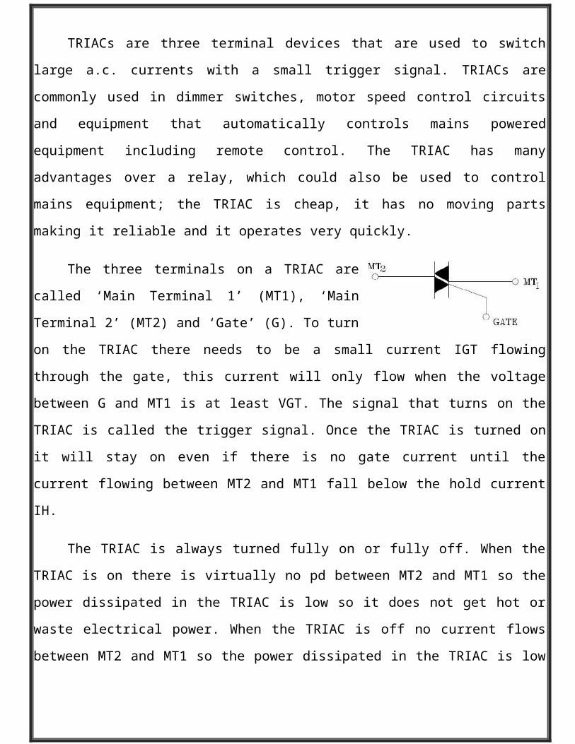
The three terminals on a TRIAC are called ‘Main
Terminal 1’ (MT1), ‘Main Terminal 2’ (MT2) and ‘Gate’
(G). To turn on the TRIAC there needs to be a small
current IGT flowing through the gate, this current will only flow when the voltage between
G and MT1 is at least VGT. The signal that turns on the TRIAC is called the trigger signal.
Once the TRIAC is turned on it will stay on even if there is no gate current until the current
flowing between MT2 and MT1 fall below the hold current IH.
The TRIAC is always turned fully on or fully off. When the TRIAC is on there is
virtually no pd between MT2 and MT1 so the power dissipated in the TRIAC is low so it
does not get hot or waste electrical power. When the TRIAC is off no current flows

between MT2 and MT1 so the power dissipated in the TRIAC is low so it does not get hot
or waste electrical power. This means that TRIACs can be small and are very efficient.
Power MOSFET:
Power MOSFET’s are generally of enhancement type only. This MOSFET is turned
‘ON’when a voltage is applied between gate and source. The MOSFET can be turned ‘OFF’
by removing the gate to source voltage. Thus gate has control over the conduction
of the MOSFET. The turn-on and turn-off times of MOSFET’s are very small. Hence they
operateat very high frequencies; hence MOSFET’s are preferred in applications such
as choppers and inverters. Since only voltage drive (gate-source) is required, the
drive circuits of MOSFET are very simple. The paralleling of MOSFET’s is easier due
to their positive temperature coefficient. But MOSFTS’s have high on-state resistance
hence for higher currents; losses in the MOSFET’s are substantially increased. Hence
MOSFET’s are used for low power applications.
Construction
Power MOSFET’s have additional features to handle larger powers. On the
n+substrate high resistivity n- layer is epitaxially grown. The thickness of n- layer
determines the voltage blocking capability of the device. On the other side of n+ substrate,
a metal layer is deposited to form the drain terminal. Now p-regions are diffused in the
epit axially grown n- layer. Further n+regions are diffused in the p- regions as shown.
2SiOlayer is added, which is then etched so as to fit metallic source and gate terminals. A
power MOSFET actually consists of a parallel connection of thousands of basic MOSFET
cells on the same single chip of silicon.
When gate circuit voltage is zero and VDD is present, n+p-
junctions are reverse biased and no current flows from drain to
source. When gate terminal is made positive with respect to
source, an electric field is established and electrons from n-
channel in the p- regions. Therefore a current from drain to
source is established.Power MOSFET conduction is due to majority carriers therefore
time delays caused by removal of recombination of minority carrier s is
removed.Because of the drift region the ON state drop of MOSFET increases. The thickness
of the drift region determines the breakdown voltage of MOSFET. As seen a parasitic
BJT is formed, since emitter base is shorted to source it does not conduct.
Power Transistor:
The need for a large blocking voltage in the off state and a high current
carrying capability in the on state means that a power BJT must have substantially
different structure than its small signal equivalent. The modified structure leads to
significant differences in the I-V characteristics and switching behavior between
power transistors and its logic level counterpart.

Power Transistor Structure:
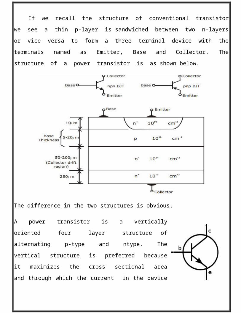
If we recall the structure of conventional transistor we see a thin p-layer is
sandwiched between two n-layers or vice versa to form a three terminal device
with the terminals named as Emitter, Base and Collector. The structure of a power
transistor is as shown below.
The difference in the two structures is obvious.
A power transistor is a vertically oriented four layer structure of alternating p-type
and ntype. The vertical structure is preferred because it
maximizes the cross sectional area and through which the
current in the device is flowing. This also minimizes on -state
resistance and thus power dissipation in the transistor.
The doping of emitter layer and collector layer is quite
large typically 1019 cm-3. A special layer called the collector drift
region (n-) has a light doping level of 1014.The thickness of the drift region determines the

breakdown voltage of the transistor. The base thickness is made as small as possible in
order to have good amplification capabilities, however if the base thickness is small
the breakdown voltage capability of the transistor is compromised.
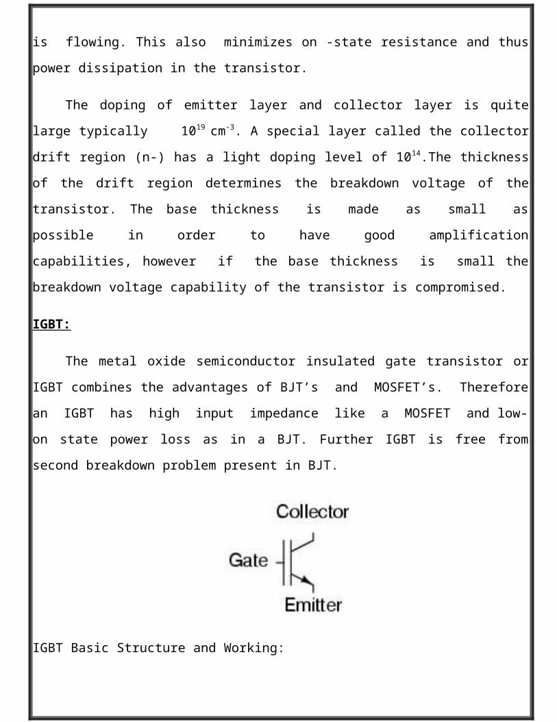
IGBT:
The metal oxide semiconductor insulated gate transistor or IGBT combines the
advantages of BJT’s and MOSFET’s. Therefore an IGBT has high input impedance like
a MOSFET and low-on state power loss as in a BJT. Further IGBT is free from second
breakdown problem present in BJT.
IGBT Basic Structure and Working:
It is constructed virtually in the same manner as a power MOSFET. However, the
substrate is now a p+layer called the collector.When gate is positive with respect to
positive with respect to emitter and with gate emitter voltage greater than VGSTH, an n
channel is formed as in case of power MOSFET. This nchannel short circuits then- region
with n+ emitter regions.An electron movement in the n- channel in turn causes substantial
hole injection from p+ substrate layer into the epitaxially n- layer. Eventually a forward
current is established.
The three layersp+ ,n- and pconstitute a pnp transistor with p+ as emitter, n- as base
and pas collector. Alson-, pand n+ layers constitute anpn transistor. The MOSFET is
formedwith input gate, emitter as source and n- region as drain. Equivalent circuit is
as shown below.
Also pserves as collector for pnp device and also as base for npn transistor. The two
pnp and npn is formed as shown.When gate is applied VGS> V GSthMOSFET turns on. This
gives the base drive to T1 . Therefore T1 starts conducting. The collector of T1 is base
of T2 . Therefore regenerative action takes place and large number of carriers are
injected into the n- drift region. This reduces the ON-state loss of IGBT just like
BJT.When gate drive is removed IGBT is turn-off. When gate is removed the induced
channel will vanish and internal MOSFET will turn-off. Therefore T1will turn-off it T2 turns
off.
Structure of IGBT is such that R1 is very small. If R1 small T1 will not conduct
therefore IGBT’s are different from MOSFET’s since resistance of drift region reduces
when gate drive is applied due to p+ injecting region. Therefore ON state IGBT is very
small.
Result:

Experiment No: 2
Date :
STATIC V-I CHARACTERISTICS OF SCR
AIM:
To plot the static V-I characteristics of the given SCR.
EQUIPMENTS AND COMPONENTS REQUIRED:
THEORY:
A silicon controlled rectifier (SCR) is the oldest and most widely used member of the
thyristor family. The SCR is a four layer pn-pn device with three junctions. It has three
terminals: anode, cathode and gate. The SCR is used essentially as a controlled switch,.
Fast switching action, small size, high reliability, low loss, high current and high voltage
Sl No Equipment/Component Specification Quantity
1 SCR-
2 Ammeters-
3 Power Supply-
4 Wattage Resistors-
5 Voltmeters-

ratings are the useful features which make the SCR suitable for power control in many
applications.
The static V-I characteristics of an SCR is shown in figure. The SCR has three modes
of operation: reverse blocking mode, forward blocking mode (off state) and forward
conduction mode (on state).
CIRCUIT DIAGRAM:
OBSERVATIONS:
VAK (V) IA (µA)

Reverse Blocking Mode:
When the cathode is positive with respect to the anode, the junctions J1 and J3 are
reverse biased and J2 is forward biased. Only a small leakage current of the order of a few
milli-amperes or micro-amperes flows and the device is in the reverse blocking mode.
When the voltage is increased to the reverse breakdown voltage, the depletion layers at
the junctions J1 and J3 breakdown and the current through the device increases to a high
value.The high current at high voltage causes more losses in the device and the junction
temperature may exceed the permissible value resulting in the damage of the device.
Forward Blocking Mode:
When the anodeis made positive with respect to thecathode, J1 and J3 are forward
biased and J2 is reverse biased. The reverse biased junction J2limits the anode current to a
few milli-amperes (forward leakage current). The SCR is then said to be in the forward
blocking mode. Application of a small positive gate current causes slight increase of
forward leakage current.
Forward conduction mode:
When the SCR is in the forward blocking mode, if the anode to cathode voltage is
increased to the forward breakdown voltage, junction J2 breaks down so that the SCR
becomes equivalent to a conducting diode. The voltage across the device falls to a small
value and the anode current is limited by the load impedance. When theforwardvoltage is
less than the forward breakdown voltage, the SCR can be triggered into conduction by
applying a pulse of positive gate current. Lower anode to cathode voltage requires higher
gate trigger current and higher anode to cathode voltage requires lower gate trigger
current. If the gate current is sufficiently large, the device can be turned on with a small
anode to cathode voltage.

PROCEDURE:
Reverse Blocking Characteristics:
Connections are made as in figure (i). Keeping the potential divider in its minimum
position, 230V supply is switched on. The cathode to anode voltage is gradually increased
and the ammeter and voltmeter readings are noted.
CIRCUIT DIAGRAM:
Observations:
Ig = 0 Ig = 0.5 Igt
VAK(V) IA (µA) VAK(V) IA (µA)

CIRCUIT DIAGRAM:
Observations:-
Determination of Vgt and Igt:
To obtain the values of the minimum values of gate voltage (Vgt) and gate current (Igt) to
turn on the thyristor, connections are made as in fig(ii). Keeping the anode resistance RA at
its maximum position and the voltage applied to the gate zero (i.e., potential divider RG at
its minimum position), the 30V power supply is switched on. With zero gate voltage, the
thyristor is in the forward blocking mode. The gate voltage is gradually increased, till the
anode current suddenly increase.The gate voltage and gate current corresponding to this
point give Vgt and Igt.
VAK (V) IA (A)

Forward Blocking Characteristics:
Connections are made as in fig(iii). Keeping the series resistance maximum and
potential divider in its minimum position, 230V supply is switched on. Keeping gate circuit
open, the anode to cathode voltage is gradually increased and the ammeter and voltmeter
readings are noted. Now the key K1 is closed and gate voltage is adjusted to get 0.5
Igtandprocedure is repeated.
ForwardConduction Characteristics:
Connections are made as in fig(iv). The gate voltage is adjusted to get sufficient gate
voltage to turn on the SCR. Now 30V supply is switched on keeping the anode resistance at
its maximum value and key K2 open. After ensuring that the SCR is conducting, the key K2
is closed. The anode current and anode to cathode voltage are noted. The anode current is
increased in steps and anode to cathode voltage is noted in each case.

RESULTS:

Experiment No: 3
Date :
R AND RC TRIGGERING CIRCUITS
AIM:
To design and setup R and RC triggering circuits for a half controlled rectifier for
different firing angles and draw relevant waveforms.
APPARATUS REQUIRED:
Sl No Apparatus/Tool Specification Quantity
1 SCR-
2 Ammeters-
3 Power Supply-
4 Wattage Resistors-
5 Voltmeters-
6 Potentiometers
7 Capacitor
8 SCR
9 Transformer
10 Bread Board
THEORY:
R Firing circuit:
Figure shows the most basic circuit. R2 is the variable resistance. Rb is the stabilizing
resistance. If R2 is zero, gate current may flow from source through R1, D and gate to
cathode. This current should not exceed maximum permissible gate current Igm. R1 can
therefore be found from the relation (Vm/R1) ≤ Igm. The function of R1 is to limit gate
current to a safe value, as R2 is varied. Resistance Rb should have such value that maximum
voltage drop across it does not exceed maximum possible gate voltage Vg. This happens
only when R2 is zero. Under these conditionV m R
R1+R2≤V gm. As resistances R1, R2 are large, gate
trigger circuits draw a small current. Diode D allows the flow of current during the
positive half cycle only i.e., gate voltage is half wave DC pulse. The amplitude of this DC
pulse can be controlled by varying R2. The potentiometer setting R2 determines the gate
voltage amplitude. When R2 is large, current I is small and voltage across Rb is Vg = I x Rb.
As Vg is less than Vgt SCR will not turn on. Trigger circuit consists of resistance only. Vg is
therefore inphase with source voltage Vs. Adjust R2 in such a way that Vg = Vgt at different
firing angles depending upon instantaneous values of input voltage. When R2 is large
enough to such that Vg become equal to Vgt only at peak value of output voltage,
corresponding firing angle will be 900. The resistance triggering cannot give firing angle
beyond 900.
Circuit Diagram:

Design:
When R2 is minimum, Ig will be maximum.
V m
R1≤ I gmax
V m=12√2V
Igmax = 100 mA
Therefore R1 ≥ VmI gmax
= 170 . (Use 220Ω Ωstd.)
When R2 is maximum, current will be minimum and voltage drop across Rb will be
maximum and it should not exceed Vgm
V m Rb
R1+Rb≤ V gmax
Rb ≤V gmax R1
V m−V gmax
Vgmax = 2.5 V, Vm = 12√2 V
Rb ≤ 2.5∗22012√2−2.5
=38 Ω(Use 33Ωstd)
When R2 = Max
V ¿=( V m
R1+R2+Rb)∗Rb
Vgt = 0.8 V, Vm = 12√2 V
R2 = 0.447 (Use 1K pot std)Ω
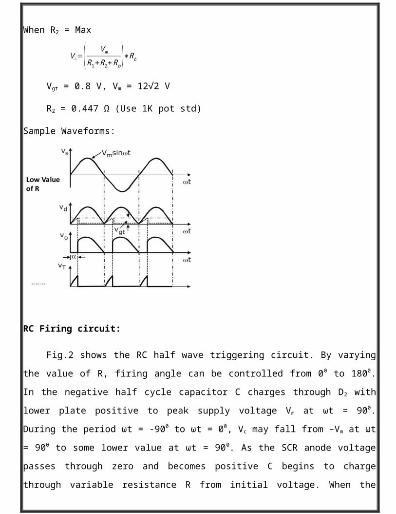
Sample Waveforms:
RC Firing circuit:
Fig.2 shows the RC half wave triggering circuit. By varying the value of R, firing angle
can be controlled from 00 to 1800. In the negative half cycle capacitor C charges through D2
with lower plate positive to peak supply voltage Vm at t = 90ω 0. During the period t = -ω900 to t = 0ω 0, Vc may fall from –Vm at t = 90ω 0 to some lower value at t = 90ω 0. As the SCR
anode voltage passes through zero and becomes positive C begins to charge through
variable resistance R from initial voltage. When the capacitor charges to positive voltage
equal to Vgt, SCR is fused and after this capacitor holds to small positive voltage. D1 is used
to prevent breakdown of cathode to gate through D2 during negative half cycle. The SCR
will trigger when Vc= Vgt+ Vd. At the instant of triggering VC is assumed constant. Hence the
maximum value of R is given byR<V S−V ¿−V d
I ¿

When the SCR triggers, voltage drop across it falls to 1 to 1.5V. This in turn lowers the
voltage drop across R and C to this low value of 1 to 1.5V. Low voltage across SCR during
conduction period keeps C discharged.
Circuit Diagram:
DESIGN:
Consider maximum firing angle to be achieved as 1600.
Vs = Vm Sin 1600 = 12√2 Sin 1600.
Igt = 200 µA
R<V S−V ¿−V d
I ¿
Vgt = 0.8 V, Vd = 0.6V
R = 22 KΩ
RC>1.3T /2

T = 20*10-3ms
C = 0.56 µF (Use 1µF std)
Sample Waveforms:
PROCEDURE
Set up the circuit on breadboard. Turn on the SCR by adjusting triggering pulse. Note
down the maximum and minimum firing angle. Observe the waveforms corresponding to
each firing angle.
RESULT:
The circuit is setup and the waveforms for various firing angles are observed and plotted.

Experiment No: 4
Date :
DIGITAL TRIGGERING CIRCUIT
AIM:
To design and set up a digital triggering circuit, suitable for triggering a single phase
half wave controlled rectifier.
EQUIPMENTS AND COMPONENTS REQUIRED:
Sl No Apparatus/Tool Specification Quantity
1 IC 741
2 IC 74121
3 Power Supply-
4 Resistors-
5 Diode
6 Potentiometers
7 Capacitors
THEORY:
The actual firing circuit of a digital firing circuit suitable for triggering a single phase
half wave controlled rectifier is shown in figure. The supply voltage is stepped down to an
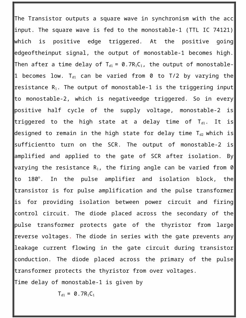
appropriate value and fed to the base of transistor Q1. The Transistor outputs a square
wave in synchronism with the acc input. The square wave is fed to the monostable-1 (TTL
IC 74121) which is positive edge triggered. At the positive going edgeoftheinput signal, the
output of monostable-1 becomes high. Then after a time delay of Td1 = 0.7R1C1, the output
of monostable-1 becomes low. Td1 can be varied from 0 to T/2 by varying the resistance R1.
The output of monostable-1 is the triggering input to monostable-2, which is negativeedge
triggered. So in every positive half cycle of the supply voltage, monostable-2 is triggered to
the high state at a delay time of Td1. It is designed to remain in the high state for delay time
Td2 which is sufficientto turn on the SCR. The output of monostable-2 is amplified and
applied to the gate of SCR after isolation. By varying the resistance R1, the firing angle can
be varied from 0 to 180o. In the pulse amplifier and isolation block, the transistor is for
pulse amplification and the pulse transformer is for providing isolation between power
circuit and firing control circuit. The diode placed across the secondary of the pulse
transformer protects gate of the thyristor from large reverse voltages. The diode in series
with the gate prevents any leakage current flowing in the gate circuit during transistor
conduction. The diode placed across the primary of the pulse transformer protects the
thyristor from over voltages.
Time delay of monostable-1 is given by
Td1 = 0.7R1C1
Maximum time delay,
Td1 (max) = 0.7R1maxC1
Since maximum time delay is 180o,
Td1 (max) = T/2, where T is the time period of the ac supply.
Thus,
R1max = T
1.4C1
Width of output pulse Td2 of monostable-2 should be sufficient to turn on the SCR.
Td2 = 0.7R2C2
Thus,
R2 =T d2
0.7C2
Suitable values of R1, C1, R2and C2are selected.
Design:
For Mono 1output,
T=0.7RC, Take C= 1 FμT(min) = 10ms
T(max) = 19ms
Rmin corresponding to 10ms, R=10×10−3
0.7×1×10−6 =14.3 kΩ=15kΩ
RmaxCorresponding to 19ms, R=19×10−3
0.7×1×10−6 =27.1 kΩ=15kΩ
Fix Rmin as fixed resistance and (Rmax –Rmin) as pot. Take15kΩ resistor and 15kΩ pot.
For Mono 2 , Assume T= 1ms and take C = 0.1 F, thenμ
R=1×10⁻³
0.7×0.1×10−6 =14.3 kΩ
Take R as 15kΩpot
Sample Waveform:
PROCEDURE:
The circuit is set up, supply is switched on. Waveforms at different points are
observed on the CRO. The firing angle is varied by varying the resistance R1. For different
firing angles, the above waveforms are observed.

RESULT:
A digital firing circuit has been designed and set up for triggering a single
phase half wave controlled rectifier.
Experiment No: 5

Date :
TRIGGER CIRCUIT USING RAMP CONTROL
AIM:
To design and set up a ramp controlled trigger circuit for a thyristor in a single phase half
wave controlled rectifier.
THEORY
For phase controlled rectifier, the trigger pulse must be synchronized with the main
supply. In ramp control circuit, the ramp generator produces a saw tooth waveform in
synchronism with main supply. This ramp is compared with a DC level in an opamp
comparator. The output of the comparator is the trigger pulse which may be directly
applied or through one amplifier and pulse transformer to the thyristor gate. The trigger
delay can be varied by varying the dc level applied to the comparator.
ZCD: The closed loop gain of the op-amp is selected high to get a square wave as output
when the input signal crosses zero.
CIRCUIT DIAGRAM:

DESIGN:
Assume the value of capacitor as 1μF.
The capacitor is charged at a constant current. Then the capacitor voltage will rise
according to the expression.
V= ¿C
Assume maximum voltage as 5v at 10ms, then,

I=CVt
=1× 10−6 ×510×10−3 =0.5mA
Assume emitter resistance voltage as about 3V. Then,
RE= 3
0.5×10−3 =6 k Ω, Take RE as 5.6k Ω
With RE=5.6k Ω , VRE=5.6×103 ×0.5× 10−3=2.8 V
Assume I2 = 0.1mA, the base current will be negligible when compared to I2
R1+R2=V CC
I 2= 12
0.1×10−3 =120k Ω
V B=V CC−V ℜ−V BE=12−2.8−0.7=8.5V
Also We have,
V B=V CC R2
R1+R2
Then,
R2=V B (R1+R2)
V CC=8.5×120
12=85 k Ω
Take R1 =33k Ω and R2 = 82k Ω
R1 =120-85 = 35k Ω
PROCEDURE: Design the ramp control circuit as per the design given above. Choose
0.5mA as the charging current of the capacitor C in the ramp generator. Set up the circuit
and test the performance.
RESULT:
A ramp control trigger circuit for a thyristor in a single phase half wave controlled rectifier
has been designed and set up.
Experiment No: 6
Date :
CHARACTERISTICS OF POWER MOSFET
AIM:
1. To obtain the output characteristics of a power MOSFET.
2. To obtain the transfer characteristics of power MOSFET
THEORY:
The power metal oxide semiconductor field effect transistor (MOSFET) is a device
derived from the field effect transistor (FET) for the use as a fast acting switch at power
levels. Unlike the bipolar transistor, which is a current controlled, the MOSFET is a voltage
controlled device. The main terminals are the drain and source. The current flow from
drain to source is being controlled by the gate to source voltage.
The absence of any stored charge makes very fast switching possible, with on and
off times being much less than 1µs. Above approximately 100V, the conduction losses are
higher for the bipolar transistor, but the switching loss is much less.
In the drain characteristics of the MOSFET, at very low values of drain source
voltage, the device has a constant resistance characteristic but at higher values of drain
source voltage, the gate voltage determines the current. However in power applications,
the drain source voltage must be small in order to minimize the on state conduction
losses.
PROCEDURE:
Set up the circuits shown in figure.

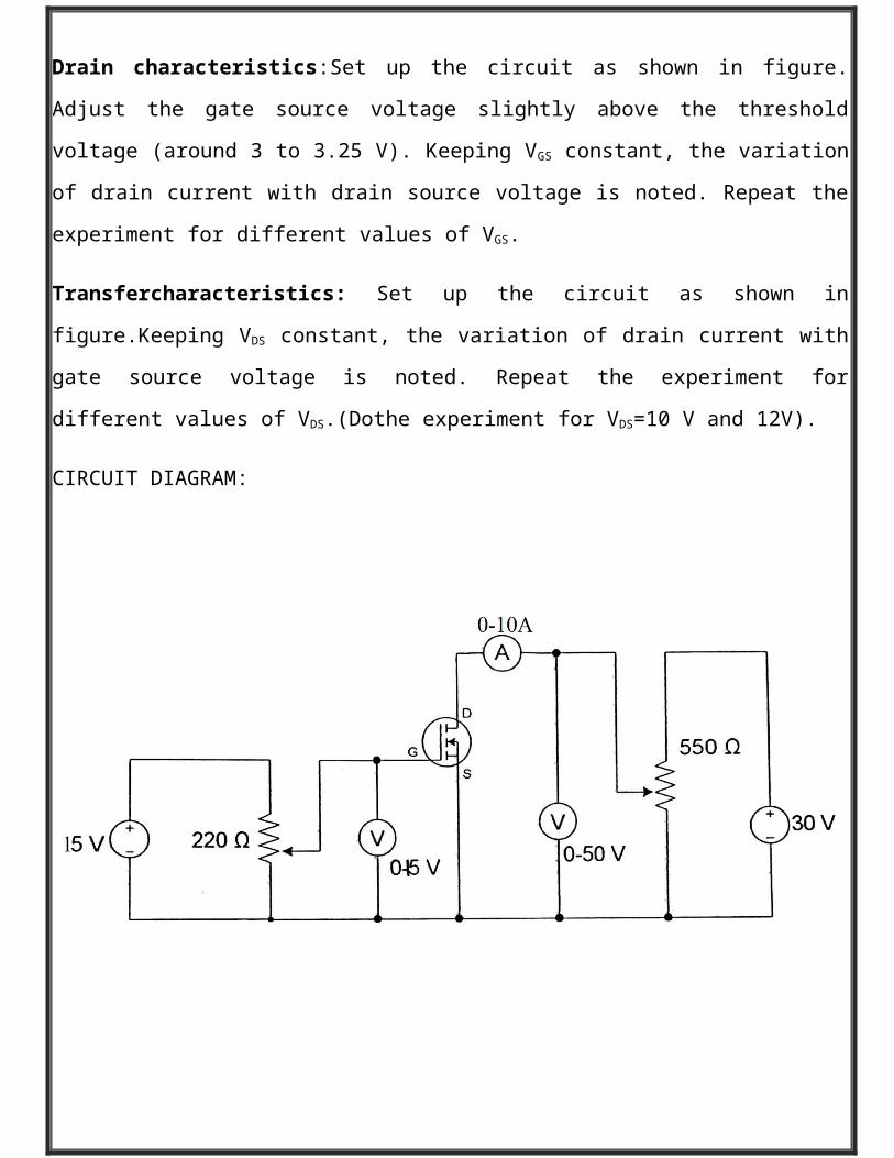
Drain characteristics:Set up the circuit as shown in figure. Adjust the gate source voltage
slightly above the threshold voltage (around 3 to 3.25 V). Keeping VGS constant, the
variation of drain current with drain source voltage is noted. Repeat the experiment for
different values of VGS.
Transfercharacteristics: Set up the circuit as shown in figure.Keeping VDS constant, the
variation of drain current with gate source voltage is noted. Repeat the experiment for
different values of VDS.(Dothe experiment for VDS=10 V and 12V).
CIRCUIT DIAGRAM:

SAMPLE WAVEFORM
OUTPUT CHARACTERISTICS TRANSFER CHARACTERISTICS
VGS = 5V VGS = 10V
ID(mA) VDS (V) ID(mA) VDS (V)
VDS = 10V VDS = 20V
VGS (V) ID(mA) VGS (V) ID(mA)

RESULT:
The drain characteristics and transfer characteristics of the given MOSFET are obtained.

Experiment No: 7
Date :
UJT FIRING CIRCUIT
AIM:
To design and set up a UJT firing circuit for a single phase half wave controlled rectifier or
single phase ac regulator.
THEORY:
The UJT is atwo layer pn device with three terminals. The terminals are called
emitter (E), base-1 (B1) and base-2 (B2). It consists of an n type silicon bar with ohmic
contacts for the two base terminals. A single p type emitter junction is formed by alloying
a p type material on the side of the silicon bar. Its structure, equivalent circuit and symbol
are shown in figure (i).
Fig(i)
With positive voltage VBB applied between B1 andB2, the potential of point A with
respect to B1 is given by
V A=V BB R1
R1+R2=
V BB R1
RBB=ηV BB

where is called the intrinsic stand off ratio. Typical values of range from 0.51 to 0.82η η
and RBB is of the order 5K to 10K . Ω Ω
The static emitter characteristic of a UJT is shown in figure (ii). When the emitter voltage
is greater than VBB, the emitter - base1 junction becomes forward biased and the emitter
current increases rapidly. Vd is the emitter diode drop (0.4 -0.7V).
Fig(ii)
Point A is called the peak point and the corresponding voltage and current are denoted by
VP and IP. the forward biased pn junction produces large number of holes in the base1
region so that the resistance drops to a very low value (about 50 ). As a result, voltageΩ
drop in R1 falls, the diode gets greater forward bias and the emitter current Ie increases as
shown by portion AB of the characteristic. In the region AB, the device exhibits negative
resistance, as an increase in emitter current is accompanied by a decrease in the emitter
voltage. At point B, E-B1 region is saturated and R1 does not decrease any more. A further
increase in Ieis accompanied by a rise in the emitter voltage as shown by the portion BC.
Point B is called the valley point; VVandIV are the corresponding emitter voltage and
emitter current. The negative resistance region between the peak point and the valley
point gives the switching characteristic so useful in generating gate trigger signals for
thyristor.
A synchronized UJT half wave trigger circuit is in figure. The output of the half wave
diode rectifier is clipped to a standard level VZ by the zener diode. The voltage

VZisappliedto the RC charging circuit. The capacitor charges at a rate determined by the
charging resistor. When the capacitor voltage reaches the peak point emitter voltage,
V P=ηV Z+V D, the E-B1 junction of UJT breaks down. As a result, the capacitor discharges
through the primary of the pulse transformer and a voltage pulse occurs at the secondary
which is fed to the gate circuit of the thyristor of a half wave controlled rectifier or a single
phase ac regulator. When the capacitor discharges the emitter circuit is turned off and the
UJT is restored to its initial state. The capacitor charges again and similar operations
repeat. The pulse repetition period is independent of the supply voltage and is given by
T=1f=RC ln ( 1
(1−η ) ). Slight variation in the pulse repetition frequency with temperature is
compensated by the resistance Rb2 connected in series with base2. The value of Rb2 is given
by Rb2=10000ηV Z
.
Even though a number of pulses are produced in a half cycle, only the first pulse will
determine the firing angle.
Since Vz goes to zero at the end of every half cycle, capacitor voltage falls to zero and
begins to charge afresh at the beginning of every half cycle. So for a given value of R1, the
time when the first pulse is applied to the SCR in a half cycle remains constant. The
synchronization of trigger pulse with the supply voltage is thus achieved.
Changing the value of R changes the instant at which the first pulse occurs. So the
firing angle can be controlled by varying R. The total range of control is around 150o. the
charging resistor R must be sufficiently small to admit the required peak point current of
the UJT.
(V Z−V P )/R> IPorR<(V Z−V P )/ IP
Since V P=ηV Z+V D ,R<[V Z (1−η )−V D ] / IP
i.e.,Rmax=[V Z (1−η )−V D ] / IP

Again the resistance R must be sufficiently large so that the emitter current does not
exceed the valley current IV.
(V Z−V V ) /R< IVorR>(V Z−V V ) /IV
Rmin=(V Z−V V ) /I V
The capacitor value should be such as to store sufficient charge to trigger the SCR. The
typical values of C are 0.1 to 0.5µF. The value of the series resistance is calculated from
R s=(V m√2−V Z) / IZmax
CIRCUIT DIAGRAM

SAMPLE WAVEFORMS:
DESIGN:
V Z=V
I P=µA
η=¿
IV=mA
V V =V
I Zmax=mA
Rmax=[V Z (1−η )−V D ]
IP=¿
Rmin=(V Z−V V )
IV=¿
T=1f=RC ln ( 1
(1−η ) )
T=ms , R=¿
Thus C= µF
R s=(V m√2−V Z) / I Zmax=¿
Rb2=10000ηV Z
=¿
PROCEDURE:
The UJT trigger circuit is set up. The supply is stepped down to a suitable value to get the
synchronizing signal, which is fed to the triggering circuit. The waveforms at various
stages are observed on the CRO for different values of firing angle.
RESULT:
A UJT firing circuit for single phase half wave controlled rectifier (single phase ac
regulator) has been designed, set up and the waveforms have been plotted.
\
Experiment No: 8
Date :
TRIGERING OF TRIAC USING DIAC
Aim: To set up a triggering circuit using DIAC for triggering a TRIAC used in a single phase
ac phase control circuit.
THEORY: The TRIAC is a bidirectional device with three terminal, two main terminals and
a gate. It is a five layer device and is equivalent to a pair of SCR’s connected in anti-parallel.
Since the TRIAC can conduct in both directions, the terms anode and cathode are not
applicable to the TRIAC. The two main terminals are designated as MT1 andMT2. MT1 is
taken as the reference point formeasurements of voltage and current at MT2 and gate. The
TRIAC is used mainly for the control of power in an circuits. With the gate open, the TRIAC
will block both half cycles of ac applied voltage. The TRIAC can be turned on in each half
cycle by a negative or positive gate current. So the TRIAC has four triggering modes.
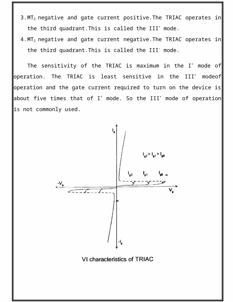
1. MT2 positive and gate current positive.The TRIAC operates in the first quadrant.This
is called the I+ mode.
2. MT2 positive and gate current negative.The TRIAC operates in the first quadrant.This
is called the I- mode.
3. MT2 negative and gate current positive.The TRIAC operates in the third
quadrant.This is called the III+ mode.
4. MT2 negative and gate current negative.The TRIAC operates in the third
quadrant.This is called the III- mode.
The sensitivity of the TRIAC is maximum in the I+ mode of operation. The TRIAC is
least sensitive in the III+ modeof operation and the gate current required to turn on the
device is about five times that of I+ mode. So the III+ mode of operation is not commonly
used.

The DIAC is a gate less device with two terminals. It is capable of blocking or
conducting current in either direction. It is used as trigger device for TRIAC gate circuits.
When MT1 is positive with respect to MT2 by a voltage greater than break over
voltage, structure P1N1P2N2 breaks over by normal thyristor action. When MT2 is positive
with respect to MT2 by a voltage greater than break over voltage, structure P2N1P2N3
breaks down and conducts current. When the device conducts the voltage across it falls to
about 3V. The circuit is energized by the transformer secondary voltage, v=V m sinωt . the
triggering device is a DIAC and the firing angle control is by varying the value of resistance
R. during the positive half cycle of the input voltage, capacitor C charges with top plate
positive. The charging rate is controlled by the resistance R. when the capacitor voltage,
V c=V ¿+V BO, where VBO is the break over voltage of the DIAC, the TRIAC will trigger,
provided the gate current Igt is available. The operation of TRIAC during the positive half

cycle is in mode I+. During the negative half cycle, the capacitor charges in the reverse
direction and a negative gate signal with respect to MT1 will trigger the TRIAC. So the
TRIAC operates in mode III-.
When the TRIAC is triggered the instantaneous voltage of the input voltage
V >V c+ I ¿R=V c=V ¿+V BO+ I ¿ R
OR
R>(V−V ¿−V BO )
I ¿
.
Taking the maximum firing angle as 120o, Rmax=0.866 V m−V ¿−V BO
I ¿
whereVm is the peak value of the line voltage. When the SCR is triggered the capacitor
voltage, V c=V ¿+V BO. But V c=V cmin+1
RC∫0
t d
V m sinωt dt where Vcmin is the initial voltage from
which the capacitor C charges and td is the time of charging of the capacitor. Since in half
cycle, the capacitor discharges through the TRIAC gate, Vcminis essentially zero.
Thus, V ¿+V BO=1
RC∫0
t d
V m sinωt dt
= 1RC
V m
ω (1−cosωt d )
For a maximum delay of 120o,
V ¿+V BO=1
Rmax C1.5V m
ω
whereω is the angular frequency in radian per second.
CIRCUIT DIAGRAM:
SAMPLE WAVEFORMS:
PROCEDURE:AC phase control circuit using TRIAC is set up. Suitable voltage is applied to
the circuit adjusting the autotransformer. Different firing angles are obtained by varying
the resistance R, for each firing angle, load voltage, voltage across SCR and DIAC are
observed on the CRO.

RESULT:A single phase voltage controller using TRIAC was set up. The waveforms of
source voltage, load voltage, voltage across SCR and voltage across DIAC are observed on
the CRO and plotted.

Experiment No: 9
Date :
IGBT CHOPPER CONTROL USING 555 TIMER
AIM:
To study and verify the chopper operation using IGBT triggered by 555 timer. Also obtain
the required waveforms and calculate duty cycle of output waveforms.
THEORY:
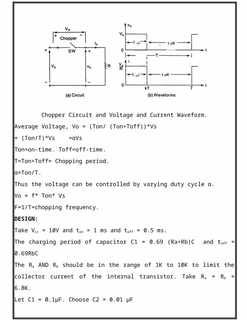
A chopper is a static power electronic device that converts fixed dc input voltage to a
variable dc output voltage. A Chopper may be considered as dc equivalent of an ac
transformer since they behave in an identical manner.
A chopper is a high speed “on" or “off” semiconductor switch. It connects source to load
and load and disconnect the load from source at a fast speed. In this manner, a chopped
load voltage as shown in Fig.1 is obtained from a constant dc supply of magnitude Vs.
During the period Ton, chopper is on and load voltage is equal to source voltage Vs. During
the period Toff, chopper is off, load voltage is zero. In this manner, a chopped dc voltage is
produced at the load terminals.
Chopper Circuit and Voltage and Current Waveform.
Average Voltage, Vo = (Ton/ (Ton+Toff))*Vs
= (Ton/T)*Vs =αVs
Ton=on-time. Toff=off-time.
T=Ton+Toff= Chopping period.
=Ton/T.αThus the voltage can be controlled by varying duty cycle .αVo = f* Ton* Vs
F=1/T=chopping frequency.
DESIGN:
Take Vcc = 10V and ton = 1 ms and toff = 0.5 ms.
The charging period of capacitor C1 = 0.69 (Ra+Rb)C and toff = 0.69RbC
The Ra AND Rb should be in the range of 1K to 10K to limit the collector current of the
internal transistor. Take Ra = Rb = 6.8K.
Let C1 = 0.1µF. Choose C2 = 0.01 µF
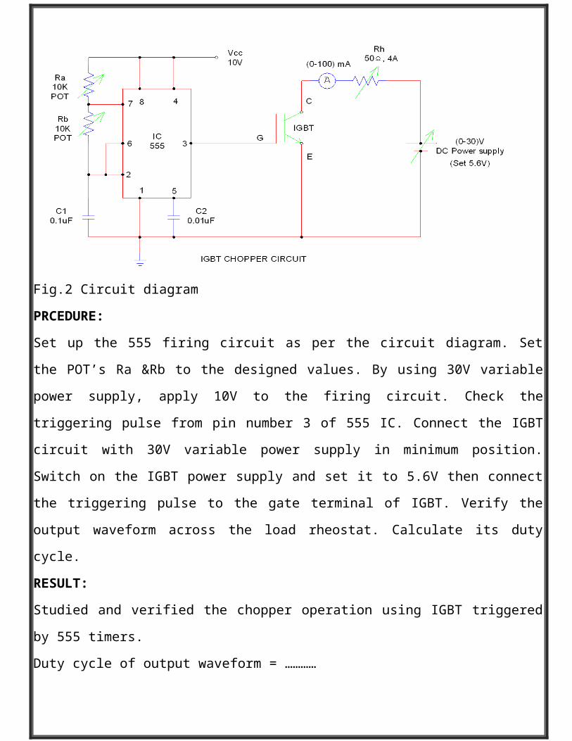
Fig.2 Circuit diagram
PRCEDURE:
Set up the 555 firing circuit as per the circuit diagram. Set the POT’s Ra &Rb to the
designed values. By using 30V variable power supply, apply 10V to the firing circuit. Check
the triggering pulse from pin number 3 of 555 IC. Connect the IGBT circuit with 30V

variable power supply in minimum position. Switch on the IGBT power supply and set it
to 5.6V then connect the triggering pulse to the gate terminal of IGBT. Verify the output
waveform across the load rheostat. Calculate its duty cycle.
RESULT:
Studied and verified the chopper operation using IGBT triggered by 555 timers.
Duty cycle of output waveform = …………
Experiment No: 10
Date :
IGBT CHARACTERISTICS
AIM:
By conducting a suitable experiment, plot the collector and drain characteristics of the
given IGBT.
THEORY:
Insulated Gate Bipolar Transistor (IGBT) is a three terminal device having a gate, collector
and an emitter. They are widely used in medium power applications such as dc and ac
motor devices, UPS systems, power supplies etc…Fig.1 shows the schematic view of an N-
channel IGBT.
Fig.1: Schematic view of an N-channel IGBT
Fig.2: IGBT Circuit Symbol
Static V-I or output or collector characteristics of anIGBT (n-channel type) show the plot of
collector current Icversus collector-emitter voltage VCE for various values of gate-emitter
voltages. These characteristics are shown in fig.3. In this characteristic the controlling
parameter is gate-emitter voltage VGE because IGBT is a voltage-controlled device.
Fig.3 Output I-V characteristics of an IGBT
The transfer characteristics if an IGBT is a plot of collector current IC versus gate-emitter
voltage VGE as shown in fig.4. This characteristic is identical to that of power MOSFET.
When VGE is less than the threshold voltage VGET, IGBT is in the off-state.
Fig.4 Transfer characteristics of IGBT
When the device is off, junction J2 blocks forward voltage and in case reverse voltage
appears across collector and emitter, junction J1 blocks it.

Fig.5 Circuit diagram
PROCEDURE:
Collector characteristics:
1. Setup the circuit as per the circuit diagram.
2. Keep the VGE at 5.5 V and vary VCE in equal steps and note down the collector current.
3. Repeat it for various values of VGE.
Transfer characteristics:
1. Setup the circuit as per the circuit diagram.
2. Make VCE = 10V. Vary VGE in equal steps and note down ID.
RESULT:
The collector characteristics and transfer characteristics of IGBT are plotted.

Experiment No: 11
Date :
SINGLE PHASE FULLY CONTROLLED BRIDGECONVERTER
AIM:
To set up a single phase fully controlled bridge converter and conduct experiment in the
setup to obtain
a) The waveforms across load and thyristor for α=600 corresponding to the
discontinuous mode of operation.
b) The load current waveforms for α=600corresponding to discontinuous mode
of operation.
c) The average output voltage α=600corresponding to continuous conduction.
Verify with theoretical value.
THEORY: Figure shows a single phase fully controlled thyristor bridge converter.
During positive half cycle of the ac supply voltage, point ‘a’ in the diagram is
positive and ‘b’ is negative. Thyristors T1 and T4 are turned on at ωt=α.Voltage across RL
load, V0 = Vab. Because of the presence of inductance in the load, load current I0 lags V0.At
ωt=π , V0 = Vab= 0. But load current has not decayed to zero. So even after ωt=π ,T1 and T4
continues to be in on state and V0 = Vabbecomes negative. Assuming discontinuous mode of
operation (corresponding to a low value of load inductance) I0 becomes zero at ωt=βand
T1 and T4 gets turned off.
V0 = Vab ; for ∝≤ ωt ≤ β
Thyristors T2 and T3 are turned on at ωt=π+∝, (after half a cycle, supply polarity is
reversed, ‘b’ becomes positive, ‘a’ becomes negative). As long asβ≤ωt ≤ π+∝, none of the
thyristors in th bridge circuit is in the on state and V0 = 0, I0 = 0. Atωt=π+∝, T2 and T3 are
turned on and V0= Vba and load current I0 lags V0. The waveforms of load voltage, load
current and thyristor voltage (VT1) corresponding to discontinuous mode are as in figure.
If the load inductance has a high value, continuous mode of operation is
obtained. in this mode, thyristor T1 and T4 which are turned on at ωt=α, continues to be in
the on state until thyristors T2 and T3 are turned on at ωt=π+∝ .So V0 = Vab ; for ∝≤ωt ≤ π+∝.
When T2 and T3 are turned on, a reverse voltage appears across T1 and T4 and they are
commutated.
V0= Vba; π+∝ . ≤ωt ≤ 2π+∝.
The same process repeats in the next half cycles of ac input voltage. The waveforms
corresponding to continuous mode of operation is shown in figure.
The average output voltage for discontinuous of operation is
V 0=1π∫α
β
V m sin ωt dωt
V 0=V m
π¿
Corresponding to continuous mode of operation, average output voltage is
V 0=1π ∫
α
π+α
V m sin ωt dωt
V 0=2V m
πcos α
PROCEDURE: Connections are made as in figure. The autotransformer is adjusted so that
the input voltage is 60 V. The firing angle of the thyristors is varied by varying the pot in
the firing module. If the thyristors do not fire interchange the input connections to the
bridge. The required waveforms are plotted.

CIRCUIT DIAGRAM

WAVE FORMS:

RESULT:
A single phase fully controlled bridge converter has been setup. the waveforms across load
and thyristor for α=600has obtained corresponding to discontinuous and continuous mode
of operation.
Experiment No: 12
Date :
PHASE LOCKED LOOPS
AIM:
To study the PLL IC NE 565 and to determine the lock in range and capture range for a free
running frequency of 2.5 kHz.
THEORY:
Phase Locked Loop is an important block of linear systems. It is a technique for
electronic frequency control. Applications are satellite communication systems, air borne
navigational systems, FM communication systems, computers etc.
A PLL consists of a phase detector, a low pass filter, an error amplifier and a voltage
controlled oscillator. VCO is a free running multivibrator and operates at a set frequency f0,
called free running frequency. If an input signal frequency,fsis applied to PLL, the phase
detector compares the phase and frequency of the incoming signal to that of the output of
VCO. If the two signals differ in frequency or in phase, an error voltage is generated. The
high frequency components are removed by the low pass filter and the difference
frequency component is amplified and applied as control voltage to VCO. This signal shifts
the VCO frequency in a direction to reduce the difference between input and output
frequencies. If fs= f0, the circuit is said to be locked. Once locked, PLL tracks the frequency
changes of the input signal. Thus PLL goes through three stages.
(i) Free running stage (ii) Capture stage (iii) Locked stage
Lock in Range: The range of frequencies over which the PLL can maintain lock with the
incoming signal is called lock in range.
Capture range: The range of frequencies over which the PLL can acquire lock with an
input signal is called capture range.

IC NE565 is available as a 14 pin DIP and a 10 pin metal can package. Pin configuration
and block diagram are given in figure. The output frequency of VCO is given by f 0=1.2
4 R1C1
Hz where R1 and C1 are external resistor and capacitor connected to pin 8 and 9. The VCO
free running frequency is adjusted with R1 and C1 to be at the center of the input
frequency. The VCO output is connected to the phase comparator by connecting pins4 and
5. A capacitor C is connected between pins 7 and 10 to make a low pass filter with an
internal resistance 3.6K.
Lock in Range, f L=±8 f 0
−V CC
Capture range, f C=±√ f L
2 π C2(3.6×10³)
PINOUT of 565
DESIGN:
Let C1=0.01 µF, C2=0.1 µF,
Free running frequency, f0= 2.5 kHz (given)
f 0=1.2
4 R1C1Hz
R1=1.2
4 ×0.01 ×10−6× 2.5× 103 =12K
Lock∈range , f L=±8 f 0
−V CC=± 8×2.5 ×103
12−(−12)=±833.33 Hz
Capture range , f C=±√ f L
2π C2(3.6×10³)=±√ 833.33
2π ×0.1×10−6(3.6×10³)=± 607 Hz
Lock in range = f3 - f1
Capture range = f2 – f4
BLOCK DIAGRAM
CIRCUIT DIAGRAM :
PROCEDURE:
Circuit is set up. First the free running frequency of the oscillator is to be determined. The
pin nos 2 and 3 are shorted and connected to the ground. The VCO output is observed at
pin no 4 and the free running frequency is measured.
To get the lock range and capture range, the VCO output is given to the phase
detector (connect pin n 4 and 5 together). The input signal is given to the pin no 2 and pin
no 3 is grounded. The phase detector compares the input signal with VCO output, any
difference in phase is amplified and fed back to VCO, which adjust the VCO output
frequency to be equal to input signal frequency. Vary the input signal frequency and
determine the range of frequencies in which the two signals are locked.
RESULT: The PLL IC 565 was studied and lock in range and capture range for a free
running frequency of 2.5KHz is found.
Lock in Range =
Capture range =