· web viewcourse structure & syllabus of master of technology (m.tech) in electronics...
TRANSCRIPT

COURSE STRUCTURE & SYLLABUS OF MASTER OF TECHNOLOGY (M.TECH)
In
Electronics & Telecommunication
Course Structure
First Year
First Semester
Paper Code
Subject
MFET1 Semiconductor Devices and ModellingMFET2 VLSI Technology and Process ModelingMFET3 Modern Digital Communication TechnologyMFET4 Digital Voice and Picture Communication
Syllabus
MSET1 : SEMICONDUCTORS DEVICES & MODELLING
1. BASIC SEMICONDUCTOR PHYSICSIntroduction, Solis-state Structure, Band Structure, Electrons and Hole: Semiconductor Statistics, Intrinsic; Extrinsic and Compensated Semiconductors, Electron and Hole Mobilities and Drift Velocities, Hall Effect and Magnetoresistance.
2. P-N JUNCTIONS, SCHOTTKY BARRIER JUNCTIONS, HETEROJUNCTIONS AND OHMIC CONTACTS
Introduction, p-n Junction Under Zero Bias Condition, Current Voltage Characteristics of an Ideal p-n Junction (The Diode Equation), Tunneling and Tunnel Diodes, Junction Breakdown – Breakdown Mechanisms; Impact Ionization and Avalanche Breakdown, Schottky Barriers, Current Voltage Characteristics of Schottky Diodes – Thermionic Emission Model; Current Voltage Characteristics : Thermionic Field Emission & Field Emission; Small-Signal Circuit of a Schottky Diode
3. BIPOLAR JUNCTION TRANSISTORSPrinciple of Operation, Minority Carrier Profiles in a Bipolar Junction Transistor, Current Components and Current Gain, Base Spreading Resistance and Emitter Current Crowding in Bipolar Junction Transistor, Effects of Non-Uniform Doping in the Base Region: Graded Base Transistors, Output Characteristics of Bipolar Junction Transistors and Early effect, Ebers-Moll Model, Bipolar Junction Transistor as a Small Signal Amplifier: Cutoff Frequencies, Bipolar Junction Transistor as a Switch, Bipolar Junction Transistors in Integrated Circuits.
4. FIELD EFFECT TRANSISTORS

Introduction, Surface Charge in Metal Oxide Semiconductor Capacitor, Capacitance-Voltage Characteristics of an MIS Structure, Metal Oxide Semiconductor Field-Effect Transistors (MOSFETs), Velocity Saturation Effects in MOSFETs, Short Channel and Nonideal Effects in MOSFETs, Subthreshold Current in MOSFETs, MOSFET Capacitances and Equivalent Circuit, Enhancemment-and Depletion-Mode MOSFETs Complementary MOSFETs (CMOS) and Silicon on Sapphire, Metal Semi-conductor Field-Effect Transistors.
MSET2 : VLSI TECHNOLOGY & PROCESS MODELLING
1. A REVIEW OF MICROELECTRONICS AND AN INTRODUCTION TO MOS TECHNOLOGY
Introduction to integrated circuit technology, The integrated circuit (IC) era, Metal-oxide-semiconductor (MOS) and related VLSI technology, Basic MOS transistors, Enhancement mode transistor action, Depletion mode transistor action, Depletion mode transistor action, nMOS fabrication, CMOS fabrication, Thermal aspects of processing, BiCMOS technology, Production of E-beam masks.
2. SUBSYSTEM DESIGN AND LAYOUTSwitch logic, Gate (restoring) logic – The inverter; Two-input nMOS; CMOS and BiCMOS Nand Gates;Two-input nMOS, CMOS and BiCMOS Nor Gates; Other forms of CMOS logic, Examples of structured design (combinational logic) – A parity generator; Bus arbitration logic for n-line bus; Multiplexers (data selectors); A general logic function block; A four-line Gray code to binary code converter; The programmable logic array (PLA), Some clocked sequential circuits – Two-phase clocking; Charge storage; Dynamic register element; A dynamic shift register.
3. SUBSYSTEM DESIGN PROCESSESSome general considerations, An illustration of design processes – The general arrangement of a 4-bit arithmetic processor; The design of a 4 – bit Shifter, Observations.
4. SOME CMOS DESIGN PROJECTSIntroduction to project work, CMOS project 1 – an incrementer / decrementer, CMOS project 2 – left / right shift serial / parallel register, CMOS project 3 – a comparator for two n-bit numbers , CMOS/BiCMOS project 4 – a two-phase non-overlapping clock generator with buffered output on both phases, CMOS projects 5 – design of a latch – an event-driven latch element for EDL systems.
5. ULTRA-FAST VLSI CIRCUITS AND SYSTEMS – INTRODUCTION TO GAAS TECHNOLOGY
Ultra-fast systems, Gallium arsenide crystal structure, Technology Development, Device modeling and performance estimation, MESFET-based design, GaAs MESFET classes of logic.
MSET3 : MODERN DIGITAL COMMUNICATION TECHNOLOGY
1. ELECTRONIC COMMUNICATION SYSTEM
Introduction, Contaminations, Noise, The Audio Spectrum, Signal Power Units, Volume Unit , Signal-To-Noise Ratio, Analog And Digital Signals, Modulation, Fundamental Limitations In A Communication System, Number Systems
2. SAMPLING AND ANALOG PULSE MODULATION
Introduction, Sampling Theory, Sampling Analysis, Types Of Sampling, Practical Sampling: Major Problems, Types Of Analog Pulse Modulation, Pulse Amplitude Modulation, Pulse Duration Modulation, Pulse Position Modulation, Signal-To-Noise Ratios In Pulse Systems
3. DIGITAL MODULATION: DM AND PCM
Introduction, Delta Modulation, Pulse.Code Modulation , PCM Reception And Noise, Quantization Noise Analysis, Aperture Time, The Ratio And Channel Capacity Of PCM, Comparison Of PCM With Other Systems, Pulse Rate, Advantages Of PCM, Codecs, 24-Channel PCM, The PCM Channel Bank, Multiplex Hierarchy, Measurements Of Quantization Noise, Differential PCM
4. DIGITAL DATA TRANSMISSION
Introduction, Representation Of Data Signal, Parallel And Serial Data Transmission, 20ma Loop And Line Drivers, Modems, Type Of Transient Noise In Digital Transmission, Data Signal: Signal Shaping And Signaling Speed, Partial Response (Correlative) Techniques, Noise And Error Analysis, Repeaters, Digital-Modulation Systems, Amplitude-Shift Keying (ASK), Frequency Shift Keying (FSK), Phase-Shift Keying (PSK), Four-Phase Or Quarternary PSK, Interface Standards
5. COMMUNICATION OVER BANDLIMITED CHANNELS
Definition And Characterization Of 4 Bandlimited Channel, Optimum Pulse Shape Design For Digital Signaling Through Bandlimited Awgn Channels, Optimum Demodulation Of Digital Signals In The Presence Of 151 And Awgn, Equalization Techniques, Further Discussion
MSET4: DIGITAL VOICE & PICTURE COMMUNICATION
1. RADIO RECEIVERSTrf and Superheat receivers, AM broadcast receivers, Communication Receivers, Tuning Indicator, Diversity reception, FM receivers.
2. NOISE Introduction, External noise, Internal noise, Noise in Communication system, Noise in AM,FM, and PM system, Noise in pulse modulated systems.

3. PROPAGATION OF WAVESReflection/ refraction of radio waves, Atmospheric absorption – Tropospheric Scatter, Ionospheric Layers, Sky Waves, Virtual Height, Regular & irregular ionospheric variations, Skip distance, Primary & Secondary Service Area.
4. BROAD BANK COMMUNICATIONSTime division multiplexing, Frequency Division multiplexing, Computer Communication System, Microwave Links, Line of Sight (LOS)links, Tropospheric Links, Satellite Communications – Choice of Orbit FDMA, TDMA, SPADE, Optical Communications – Modulation and Detection, Integrated service digital network (ISDN).
5. PICTURE-SIGNAL TRANSMISSION AND RECEPTIONFacsimile-transmission and reception, Television-scanning process, CCIR-B standards, TV camera systems – image orthicon and vidicon –transmission and reception principle for black and white TV signals, Principle of color TV – primary colours, colour TV systems – NTSC, SECAM, PAL, Transmission and reception using PAL system, PIL Picture tube.
6. RECORDING AND DIGITAL PROCESSING OF VIDEO SIGNALSBasic Video recording principles, Recording of luminance signals, Recording of Chrominance signal, Frequency range of the VHS signal, Tape loading, Tape format in VHS systems, Operating modes of a video cassette recorder, E-E mode, Playback mode, Digital processing of Video Signals, How much digital is the Digital TV? Video processor, Audio Processing, Control Computer, CD Players

COURSE STRUCTURE & SYLLABUS OF MASTER OF TECHNOLOGY (M.TECH)
In
Electronics & Telecommunication
Course Structure
First Year
Second Semester
Paper Code
Subject
MFET5 Solid State CircuitsMFET6 Digital Circuits & Systems MFET7 Optimal ControlMFET8 Satellite Communication System
Syllabus
MFET5 SOLID STATE CIRCUITS
1. TRANSISTOR SWITCHING:Objectives, Introduction, Ideal Transistor Switch , Practical Transistor Switch, Transistor Switching Times, Improving the Switching Times, Direct- Coupled Inverter, Capacitor-Coupled Inverter, Capacitor –Coupled Inverter Circuits, Junctions FET Switching Circuits, MOSFET Switching Circuits, Review Questions, Problems. Laboratory Exercise, Laboratory Exercise.
2. IC OPERATIONAL AMPLIFIERS IN SWITCHING CIRCUITS: Objectives, Introduction, IC Operational Amplifiers , Op-Amps as Linear Amplifiers, Op-
Amps in Switching Circuits, Op-Amp Inverters, Op-Amps Clipper Circuits, Op-Amp Differentiator, Miller Integrator Circuit, Review Questions, Problems,.Laboratory Exercise, Laboratory Exercise , Laboratory Exercise.
3. SCHMITT TRIGGER CIRCUIT AND VOLTAGE COMPARATIONS: Objectives, Introduction, Transistor Schmitt Trigger Circuit, Designing for the
UTP,Designing for the UTP and LTP, Speed Up Capacitor, Output/Input Characteristics, Op-Amp Schmitt Trigger Circuits, IC Schmitt, IC Voltage Comparators, Review Questions, Problems, Laboratory Exercise, Laboratory Exercise.
4. MONOSTABLE AND ASTABLE MULTIVIBRATORS:Objectives, Introduction, Collector- Coupled Monostable Multivibrator, Designing a Monostable Multivibrator, Triggering Monostable Multivibrators,Emitter-Coupled Monostable Multivibrators, Op- Amp Monostable Multivibrators, Astable Multivibrators,

Voltage Comparator as Monostable and Astable , Review Questions, Problems, Laboratory Exercise, Laboratory Exercise.
5. IC TIMER CIRCUITS:Objective , Introduction, The 555 IC Timer, 555 as a Monostable Multivibrator, Designing a 555 Monostable Circuit, Modification to the Basic 555 Monostable Circuit, 555 Astable Multivibrator, Modifications to the Basic 555 Astable Circuit, More 555 Timer Applications, CMOS Timer Circuit, Review Questions, Problems, Laboratory Exercise , Laboratory Exercise.
6. RAMP, PULSE AND FUNCTION GENERATORS:Objective, Introduction, RC Ramp Generator, Constant- Current Ramp Generator, ,UJT Relaxation Oscillators, Bootstrap Ramp Generators, Free –Running Ramp Generators, Miller Integrator Ramp Generators, Triangular Waveform Generators, Pulse Generator Circuit, Op – amp Function Generator, Review Questions, Problems, Laboratory Exercise , Laboratory Exercise, Laboratory Exercise.
7. INTEGRATED CIRCUIT LOGIC GATES:Objectives, Introduction, Logic Gate Performance Factors, DTL, HTL, and RTL,Standard TTL, Open – Collector TTL , Tri-State TTL ( TSL), Other TTL Types, Emitter – Coupled Logic (ECL), P-MOS and N-MOS Logic Gates, CMOS Logic Gates, Integrated Injection Logic (I L) Comparison of Major IC Logic Types , Interfacing Different Logic Types, Review Questions, Problems, Laboratory Exercise, Laboratory Exercise , Laboratory Exercise.
8. BISTABLE MULTIVIBRATORS (FLIP-FLOPS):Objectives, Introduction, Transistor Collector- Coupled Bistable, Emitter – Coupled Bistable, Bistable Triggering, The T Flip- Flop, The SC Flip Flop, The Clocked SC Flip-Flop, The D Flip Flop, The D Flip- Flop, The JK Flip Flop, Master Slave Flip-Flops, Review Questions, Problems, Laboratory Exercise, Laboratory Exercise.
9. SAMPLING , CONVERSION, MODULATION AND MULTIPLEXING:Objectives, Introduction , Sampling Gates, Sample- and Hold Circuit, Digital-to –Anolog Conversation, Pulse Modulation, Time Division Multiplexing, Pulse Code- Modulation and Demodulation, Review Questions, Problems, Laboratory Exercise, Laboratory Exercise, Laboratory Exercise.
MFET6 DIGITAL CIRCUITS AND SYSTEMS
1. LOGIC GATES AND BOOLEAN ALGEBRA:Boolean Constants, Variables and Functions, Truth Table and Timing diagram: Truth Table; Timing Diagram, Logic Gates, Boolean expressions for Logic Circuits: Determining Output Expressions. Constructing Logic Diagrams, Boolean algebra Laws and Rules: Boolean Laws, Rules for Boolean Algebra , Demorgan’s Theorems, Canonical or Standard Forms for Boolean Functions: Standard Sum of Products Form; Standard Product of Sum Forms; Conversion between Standard or Canonical Forms;, Karnaugh Map: K.Map Format; Plotting; Boolean Expression; Grouping Cells for Simplification; Plotting Truth Table Functions; “Do not care” Conditions; Multiple Output Function Minimization, Universal Property of the NAND and NOR Gates, NAND and NOR Implementation: NAND Implementation; NOR Implementation, Quine MC Cluskey

Method: Determining Price Implicants; Determining Essentials Prime Implicants of Minimal Cover; Cyclic Prime Implicant Chart, Exercises.
2. DIGITAL LOGIC FAMILIES:Digital Integrated Circuits, Characteristics of Digital IC’s, Positive and Negative Logic, High Active and Low Active Signals, Digital Logic Families, Diode Logic, Direct Coupled Transistor Logic (DCTL), Resistor Transistor Logic (RTL), Diode Transistor Logic (DTL), High Threshold Logic (HTL), Integrated Injection Logic (IIL), Transistor Transistor Logic (TTL): Unused Inputs; Advantages and Disadvantages of TTL, Emitter coupled Logic(ECL), Unipolar Logic Policies: PMOS and NMOS Circuits; CMOS Circuits, Interfacing TTL and CMOS, Comparison of Logic Families, Exercise.
3. COMBINATIONAL AND ARITHMETIC LOGIC CIRCUITS:Combinational and Sequential Circuit, Adders: Half Adder; Full Adder; Parallel Adder; Look Ahead Carry Adder; Serial Adder; BCD Adder; IC Adders, Subtractor: Half Subtractor; Full Subtractor; Two’s Complement adder/subtractor, Encoder: Decimal to BCD Encoder; Switch encoder; Octal to Binary encoder, Decoders: 1 of 8 Decoders; BCD to Decimal Decoders; BCD to Seven Segment Decoder, Code Converter: Excess 3 code converter; Binary to Gray Code Converter, Multiplexers: Basic two Input Multiplexers; Four input multiplexers; Eight input multiplexers; IC multiplexers, Boolean Function Implementation; Application of multiplexers, Demultiplexers: 1 line to 4 line Demultiplexers, Demultiplexers ICs; Applications of Demultiplexers, Magnitude Comparator, Parity Generator/Checker, Multiplier, Dividers, Arithmetic Logic Unit, Static Hazards, Exercise.
4. WAVE SHAPING CIRCUITS:Introduction, Linear Wave Shaping Circuits: The High Pass RC(differentiator) Circuit; Integrator, Application of Linear Wave Shaping Circuits, Non Linear Wave Shaping Circuits: Clipping or Limiting Circuits; Clamping Circuits; Transistor Clamping Circuits, Exercise.
5. FLIP FLOP AND TIMING CIRCUITS:Latches: SR Latch; Gated SR Latch; Gated D Latch, Gated Flip Flop: Clock Pulse Triggering; Edge Triggered SR flip-flop; Edge Triggered JK flip-flop; Edge Triggered D flip-flop; Edge Triggered T flip-flop, Integrated Circuit flip-flop, Race around problem, The Master Slave JK flip flop, Difference between Latch and flip flop, Flip Flop Parameters, Flip Flop excitation table, Application of Flip Flop, Multivibrators, Bistable Multivibrators: Commutating or Speed up Capacitors; Triggering, Astable Multivibrator: Gated Astable Multivibrator; Schmitt Trigger Astable Multivibrator, Monostable Multivibrator IC’s: Gated Monostable Multivibrator; Monostable Multivibrator ICs; Schmitt Trigger Monostable Multivibrator, Schmitt Trigger, The 555 Timer, Exercise.
6. SEMICONDUCTOR MEMORIES:Memory Organisation, Classification of Memories, Read only memory: Mask Programmable ROM(M ROM); Programmable ROM; Reprogrammable Read Only Memory; ROM Applications, Random Access Memory: Static RAM; Dynamic RAM; RAM IC; Application of RAM, CCD Memories, Content Addressable Memory, Memory Expansion, Memory Address Decoding, Programmable Logic Devices, PROM as PLD, Programmable Array Logic (PAL): PAL Devices, Programmable Logic Array (PLA),

Field Programmable Gate Array (FPGA): Logic Cell Array; The Actel ACT; The Plessey ERA, Exercise.
7. A/D AND D/A CONVERTERS:Representation of an Analog Signal in Digital form, Operational amplifier Basics, Digital to Analog Conversion, Binary Weighted Resistance D/A converter, R-2R Ladder D/A converter, Performance Characteristics of D/A converters, Applications of D/A converters, Integrated Circuit D/A converters, Sample and Hold Circuits, Analog Switches and Multiplexers, Analog to Digital Conversion, Simultaneous A/D Conversion, simultaneous A/D conversion, Stair Step Ramp Conversion, Tracking A/D converter, Single Slope A/D converter, Dual Slope A/D converter, Voltage to Frequency A/D converter, Successive Approximation A/D converter, Integrated Circuit Analog to Digital Converter, Performance Characteristics of A/D converter, Exercise.
MFET7 : OPTIMAL CONTROL 1 : INTRODUCTION TO CONTROL SYSTEM1.1 Classification Of Systems1.2 Open-Loop Control System1.3 Closed-Loop Control Systems1.4 Elements Of Automatic Or Feedback Control System1.5 Requirement Of Automatic Control Systems
2 : MATHEMATICAL MODELS OF CONTROL SYSTEM2.1 Representation Of a Control System2.2 Description Of Some Of Typical Physics System2.3 Tachnogenerators2.4 Potentiometers, LVDT and Synchros2.5 Synchros2.6 Hydraulic Actuation
3: BASIC PRINCIPLES OF FEEDBACK CONTROL3.1 The Control Objectives3.2 Feedback Control System Characteristics3.3 Proportional Mode Of Feedback Control3.4 Integral Mode Of Feedback Control3.5 Derivatie Mode Of Feedback Control
4 : TIME DOMAIN ANALYSIS AND FREQUENCY RESPONSE4.1 Standard Test Signals4.2 Static Accuracy4.3 Computation Of Steady State Errors4.4 Transient Response: First Order System4.5 Transient Response: Second Order System4.6 Transient Response Specification4.7 Conclusion4.8 Frequency Response4.9 Frequency Domain Specifications4.10 Magnitude And Phase Angle Characteristics Plot

4.11 Frequency Response Specification4.12 Representation Sinusoidal Transfer Function
5. CONCEPTS OF STABILITY AND THE ROUTH STABILITY CRITERION5.1 Bounded-Input Bounded-Output Stability5.2 Zero-Input Stability5.3 The Routh Stability Criterion
6: NYQUIST STABILITY CRITERION6.1 Stability Margin6.2 Phase Margin
7: BODE PLOTS
8: ROOT LOCUS8.1 The transfer function of a second order control system8.2 GENERAL RULES
MFET8 SATELLITE COMMUNICATION SYSTEM
1. PRINICPLES OF SATELLITE COMMUNICATIONS:Evolution and Growth of Communication Satellite, Synchronous Satellite, International Regulation and Frequency Co-ordination, Satellite Frequency Allocation and Bank Spectrum, General and Technical Characteristics of a Satellite Communication System, Advantages of Satellite Communication, Active and Passive Satellite , Advent of Digital Satellite Communication, Modem and Codec, Review Questions, Reference.
2. DIGITAL SATELLITE TRANSMISSION:Advantages of Digital Communication, Byte, Baud , Elements of Digital Satellite Communication Systems, Digital Baseband Signals, Digital Modulation Techniques, Satellite Digital Link Design, Time Division Multiplexing , UST, 24- Channel System, Review Questions, Reference.
3. MULTIPLE ACCESS TECHNIQUES:Introduction, Time Division Multiple Acces ( TDMA) , TDMA, Frame Structures, TDMA Burst Structures,TDMA Frame Efficiency, TDMA Superframe, TDMA Frame Acquisition and Synchronization, TDMA Compared to FDMA, TDMA Burst Time Plan, Mutiple Beam (Satellite Switched) TDMA Satellite Systems, Beam Hopping ( Transponder Hopping)TMDA, Code Division Multiple Access (CDMA) and Hybrid Access Techniques, Suggested References, Review Questions.
4. DEMAND ASSIGNMENT MULTIPLE ACCESS TECHNIQUES: Introduction , Erlang call congestion ( Blocking or B) Formula, Demand Assignment Control , DA- FDMA ( Spade) System, Demand Assignment TDMA (DATDMA) Digital Speech Interpolation, Review Questions, References.
5. SPREAD SPECTRUM TECHNIQUE AND CODE DIVISION MULTIPLE ACCESS:
Introduction , Process Gain and Jam Margin, J/S Ratio and Antijam Margin, Direct Sequence Spread Spectrum Techniques , PN Sequency, DS- CDMA, Frequency Hopping
Spread Spectrum Communication System (FM-SS), Frequency Hopping Spread Spectrum Code- Division Multiple Access (FH-SS-CDMA), Synchronization, Application of Spread Spectrum Techniques, Hybrid Systems, Review Questions.
6. SATELLITE ORBITS AND INCLINATION:Introduction, Synchronous Orbit, Orbital Parameters, Satellite Location With Respect to the Earth , Look Angles, Earth Coverage and Slant Range, Eclipse Effects, Satellite Placement in Geostationary Orbit, Station Keeping, Satellite Stabilization, Review Questions, References.
7. COMMUNICATION SATELLITE SUBSYSTEMS: Introduction, Electric Power Supply, Attitude and Orbit Control , Propulsion Sub System, Repeaters, Antenna Systems, Telemetry , Tracking and Command (TTC) Subsystem, Thermal Control System, Structure Subsystem, Reliability of Satellite Subsystems, Review Questions, References.
8. SATELLITE EARTH STATIONS: Introduction, Earth Station Design Requirement, Earth Station Subsystems, Monitoring and Control, Frequency Coordination , Small Earth Station, Very Small Aperture Terminals (VSATs), Mobile and Transport Earth Stations, Earth Stations in Near Future, TVRO Systems (Television Receive Only Systems), Review Questions, References.
9. SATELLITE AND CABLE TRANSMISSION SYSTEMS:Introduction, Cable Channel Frequencies, Head- End Equipment, Distribution of the Signal , Important Cable Television Network Specifications, Network Architecture, Optical Fibre CATV Systems, Indian Perspective, Future of Cable TV Systems, Reference.
10. SPEECH CODING TECHNIQUEES :Introduction, Some Facts about Speech, Digital Speech Quality and International Digital Telephony Standards, Basic Speech Coding Methods, Low Bit Rate Speech Coding, Audio Coding, Hardware Technology in Speech Coding, Speech Coder Performance.

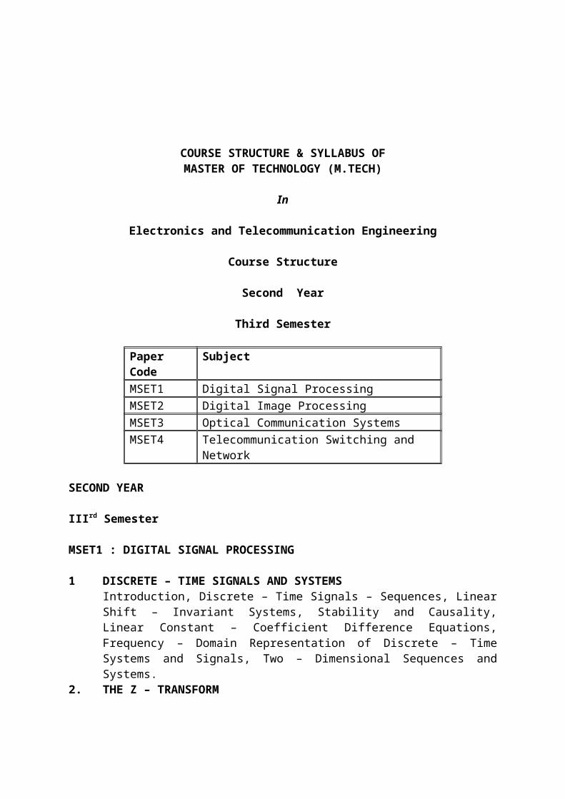
COURSE STRUCTURE & SYLLABUS OF MASTER OF TECHNOLOGY (M.TECH)
In
Electronics and Telecommunication Engineering
Course Structure
Second Year
Third Semester
Paper Code Subject
MSET1 Digital Signal ProcessingMSET2 Digital Image Processing MSET3 Optical Communication Systems MSET4 Telecommunication Switching and Network
SECOND YEAR
IIIrd Semester
MSET1 : DIGITAL SIGNAL PROCESSING
1 DISCRETE – TIME SIGNALS AND SYSTEMSIntroduction, Discrete – Time Signals – Sequences, Linear Shift – Invariant Systems, Stability and Causality, Linear Constant – Coefficient Difference Equations, Frequency – Domain Representation of Discrete – Time Systems and Signals, Two – Dimensional Sequences and Systems.
2. THE Z – TRANSFORM Introduction, z- Transform, Inverse z- Transform, z- transform Theorems and Properties, System Function, Two- Dimensional Z- Transform, Summary,
3 THE DISCRETE FOURIER TRANSFORMIntroduction, Representation of Periodic Sequences- The Discrete Fourier Series, Properties of Discrete Fourier Series, Summary of Properties of the DFS Representation of Periodic Sequences, Sampling the z- Transform, Fourier Representation of Finite- Duration Sequences- The Discrete Fourier Transform, Properties of Discrete Fourier Transform, Summary of Properties of the Discrete Fourier Transform, Linear Convolution Using the Discrete Fourier Transform, Two- Dimensional Discrete Fourier Transform, Summary.
4 FLOW GRAPH AND MATRIX REPRESENTATION OF DIGITAL FILTERSIntroduction, Signal Flow Graph Representation of Digital Networks, Matrix Representation of Digital Networks, Basic Network Structures for IIR Systems, Transposed Forms, Basic Network Structures for FIR Systems, Parameter Quantization Effects, Tellengen’s Theorem for Digital Filters and Its Applications, Summary.

5 DIGITAL FILTER DESIGN TECHNIQUESIntroduction, Design of IIR Digital Filters from Analog Filters, Design Examples : Analog- Digital Transformation, Computer- Aided Design of IIR Digital Filters, Properties of FIR Digital Filters, Design of FIR Filters Using Windows, Computer- Aided Design of FIR Filters, A comparison of IIR and FIR Digital Filters, Summary.
6 COMPUTATION OF THE DISCRETE FOURIER TRANSFORMIntroduction, Goertzel Algorithm, Decimation-in–Time FFT Algorithms, Decimation-in-Frequency FFT Algorithms, FFT Algorithms for N a Composite Number, General Computational Considerations in FFT Algorithms, Chirp Z- Transform Algorithm, Summary.
MSET2 : DIGITAL IMAGE PROCESSING
1. CONTINUOUS IMAGE MATHEMATICAL CHARACTERIZATION
Image Representation, Two-Dimensional Systems, Two-Dimensional Fourier Transform, Image Stochastic Characterization
2. PSYCHOPHYSICAL VISION PROPERTIESLight Perception, Eye Physiology, Visual Phenomena, Monochrome Vision Model, Color Vision Model
3. PHOTOMETRY AND COLORIMETRYPhotometry, Color Matching, Colorimetry Concepts, Tristimulus Value Transformation
4. IMAGE SAMPLING AND RECONSTRUCTIONImage Sampling And Reconstruction Concepts, Image Sampling Systems, Image Reconstruction Systems
5. DISCRETE IMAGE MATHEMATICALCHARACTERIZATIONVector-Space Image Representation, Generalized Two-Dimensional Linear Operator, Image Statistical Characterization, Image Probability Density Models, Linear Operator Statistical Representation
6. IMAGE QUANTIZATIONScalar Quantization, Processing Quantized Variables, Monochrome And Color Image Quantization
7. SUPERPOSITION AND CONVOLUTIONFinite-Area Superposition And Convolution, Sampled Image Superposition And Convolution, Circulant Superposition And Convolution, Superpositon And Convolution Operator Relationship
8. UNITARY TRANSFORMSGeneral unitary transforms, fourier transform, cosine, sine, and hartley transforms, hadamard, haar, anddaubechies transforms, karhunen-loeve transform

9. IMAGE ENHANCEMENTContrast Manipulation, Histogram Modification, Noise Cleaning, Edge Crispening, Color Image Enhancement, Multispectral Image Enhancement10. IMAGE RESTORATION MODELSGeneral Image Restoration Models, Optical Systems Models, Photograpidc Process Models, Discrete Image Restoration Models
11. MORPHOLOGICAL IMAGE PROCESSINGBinary Image Connectivity, Binary Image Hit Or Miss Transformations, Binary Image Shrinking, Thinning, Skeletonizing, And Thickening, Binary Image Generalized Dilation And Erosion, Binary Image Close And Open Operations, Gray Scale Image Morphological Operations
12. EDGE DETECTIONEdge, line, and spot models, first-order derivative edge detection, second-order derivative edge detection, edge-fitting edge detection, luminance edge detector performance, color edge detection, line and spot detection
13. IMAGE FEATURE EXTRACTIONImage feature evaluation, amplitude features, transform coefficient features, texture definition, visual texture discrimination MSET3 : OPTICAL COMMUNICATION SYSTEMS
1.........ELEMENTARY DISCUSSION OF PROPAGATION IN DIELECTRIC WAVEGUIDES
1.1 Introduction1.2 Step-index fibers: numerical aperture and multi path dispersion 1.3 Propagation and multipath dispersion in graded-index fibers 1.4 Modes and rays1.5 The slab waveguide
2 MATERIAL DISPERSION2.1 Refractive index: theory2.2 The refractive indices of bulk media: experimental values 2.3 Time dispersion in bulk media2.4 The wavelength of minimum dispersion
3 ATTENUATION MECHANISMS IN OPTICAL FIBERS3.1 Introduction3.2 Absorption3.3 Scattering3.4 Other very low-loss materials3.5 All-plastic and polymer-clad-silica (PCS) fibers 3.6 Damage by ionizing radiation
4 SYSTEM CONSIDERATIONS 4.1 The optimum wavelength for silica fibers4.2 The ultimate bandwidth limitation

4.3 A comparison between optical fibers and conventional electrical transmission lines
5 SINGLE-MODE FIBERS5.1 Types of single-mode fiber
5.1.1 Introduction5.1.2 Standard single-mode fiber 5.1.3 Dispersion-shifted fiber5.1.4 Dispersion-flattened fiber5.1.5 Practical fiber profiles
5.2 Mode spot size5.3 HE 11 mode propagation characteristics
6 THE FABRICATION OF FIBERS, CABLES AND PASSIVE COMPONENTS6.1 Fiber production methods
6.1.1 Introduction6.1.2 Crucible methods6.1.3 Vapour deposition methods6.1.4 Fiber pulling and coating6.1.5 Comparison between vapour deposition methods
6.2 Fiber strength6.3 Cables6.4 Splices and connectors
6.4.1 Introduction6.4.2 Splices6.4.3 Connectors6.4.5 Couplers
7 FIBER PARAMETERS: SPECIFICATION AND MEASUREMENT7.1 Introduction7.2 The refractive-index profile7.3 Near- and far-field intensity distributions 7.4 Attenuation measurements7.5 Bandwidth measurements7.6 Cutoff wavelength
8 THE DESIGN OF LEDS FOR OPTICAL COMMUNICATION8.1 The external quantum efficiency8.2 The Burrus-type double heterostructure surface-emitting LED (DH-SLED)8.3 The stripe-geometry, edge-emitting LED (ELED) 8.4 LED-to-fiber launch efficiency8.5 Lensed LED-to-fiber launch systems8.6. LED designs
9 SEMICONDUCTOR LASERS9.1 The theory of laser action in semiconductors
9.1.1 The condition for gain9.1.2 Rates of stimulated and spontaneous emission9.1.3 The effect of refractive index9.1.4 Calculation of the gain coefficient9.1.5 The relation of the gain coefficient to the current density
9.2 Some simplified calculations9.2.1 An estimate of the gain coefficient9.2.2 Theoretical variation of the gain coefficient9.2.3 The threshold current density9.2.4 The differential quantum efficiency
9.3 Modulation frequency response9.3.1 Small signal frequency response9.3.2 Step response9.3.3 Frequency modulation (chirp)
9.4 Noise in semiconductor lasers
10 SEMICONDUCTOR LASERS FOR OPTICAL FIBER COMMUNICATION SYSTEMS
10.1 Introduction10.2 Methods for obtaining the stripe geometry10.3 Optical and electrical characteristics of Fabry-Perot lasers
10.3.1 Spectral characteristics10.3.2 Power and voltage characteristics
10.4 Quantum-well lasers and laser arrays10.5 Single frequency semiconductor lasers
10.5.1 Introduction10.5.2 Distributed feedback (DFB) lasers
10.6 The reliability of DH semiconductor LEDs and lasers10.7 The transmitter module
11 THE RECEIVER AMPLIFIER11.1 Introduction11.2 Sources of receiver noise11.3 Circuits, devices and definitions11.4 Signal-to-noise ratio in the voltage amplifier circuit11.5 Signal-to-noise ratio in the transimpedance feedback amplifier 11.6 The ideal quantum-limited receiver11.7 Amplifier design examples
11.7.1 High input resistance or integrating amplifier11.7.2 Voltage amplifier with low input resistance11.7.3 Explicit solution11.7.4 A worked example
12 THE REGENERATION OF DIGITAL SIGNALS12.1 Causes of regeneration error
12.1.1 The ideal digital system 12.1.2 Causes of regeneration error12.1.3 Filter Characteristics designed to minimize intersymbol interference12.1.4 The eye diagram
12.2 The quantum limit to detection12.3 The effect of amplifier noise and thermal noise on the error probability
12.3.1 Probability of error when shot noise is negligible12.3.2 Probability of error when multiplied shot noise is comparable to other
sources of noise12.3.3 System Optimization

12.4 Noise penalties in practical system12.4.1 Introduction12.4.2 Non – zero extinction ratio12.4.3 Finite pulse width and timing jitter12.4.4 Power amplitude variations : modal noise
13 OPTICAL FIBER COMMUNICATION SYSTEMS13.1 Introduction13.2 The economic merits of optical fiber systems
13.2.1 An overview13.2.2 Telecommunications13.2.3 Local distribution services13.2.4 Computer networks, local data transmission and telemetry
13.3 Digital optical fiber telecommunication systems13.3.1 Introduction13.3.2 First generation systems13.3.3 Second generation systems13.3.4 Future systems
13.4 Data communication networks13.4.1 Introduction13.4.2 Network topologies13.4.3 Medium access control protocols13.4.4 System examples
13.5 Analog systems13.5.1 Advantages and disadvantages of analog modulation 13.5.2 Direct intensity modulation at baseband13.5.3 The use of a frequency-modulated subcarrier
13.6 The optical ether
MSET4 TELECOMMUNICATION SWITCHING AND NETWORKS
1 INTRODUCTION1.1 Evolution of Telecommunications 1.2 Simple Telephone Communication 1.3 Basics of a Switching System 1.4 Manual Switching System1.5 Major Telecommunication Networks 2 STROWGER SWITCHING SYSTEMS2.1 Rotary Dial Telephone 2.2 Signalling Tones2.3 Strowger Switching Components 2.4 Step-by-Step Switching 2.4 Design Parameters2.5 100-line Switching System 2.6 1000-line Blocking Exchange 2.8 10,OOO-line Exchange

3 CROSSBAR SWITCHING3.1 Principles of Common Control 3.2 Touch Tone Dial Telephone 3.3 Principles of Crossbar Switching3.4 Crossbar Switch Configurations 3.5 Crosspoint Technology 3.6 Crossbar Exchange Organisation
4 ELECTRONIC SPACE DIVSION SWITCHING4.1 Stored Program Control 4.2 Centralised SPC 4.3 Distributed SPC 4.4 Software Architecture 4.5 Application Software 4.6 Enhanced Services 4.7 Two-Stage Networks 4.8 Three-Stage Networks 4.9 n- Stage Networks
5 TRAFFIC ENGINEERING5.1 Network Traffic Load and Parameters.5.2 Grade of Service and Blocking Probability 5.3 Modelling Switching Systems5.4 Incoming Traffic and Service Time Characterisation 5.5 Blocking Models and Loss Estimates5.6 Delay Systems
6 TELEPHONE NETWORKS6.1 Subscriber Loop Systems 6.2 Switching Hierarchy and Routing 6.3 Transmission Plan 6.4 Transmission Systems 6.5 Numbering Plan6.6 Charging Plan6.7 Signalling Techniques 6.8 Inchannel Signalling 6.9 Common Channel Signalling 6.10 Cellular Mobile Telephony
7 DATA NETWORKS7.1 Data Transmission in PSTNs7.2 Switching Techniques for Data Transmission 7.3 Data Communication Architecture7.4 Link-to-Link Layers7.5 End-to-End Layers7.6 Satellite Based Data Networks7.7 Local Area Networks7.8 Metropolitan Area Networks

7.9 Fibre Optic Networks7.10 Data Network Standards7.11 Protocol Stacks7.12 Internetworking
8 INTEGRATED SERVICES DIGITAL NETWORK8.1 Motivation for ISDN8.2 New Services8.3 Network and Protocol Architecture 8.4 Transmission Channels8.5 User-Network Interfaces8.6 Signalling8.7 Numbering and Addressing8.8 Service Characterisation8.9 Interworking8.10 ISDN Standards8.11 Expert Systems in ISDN8.12 Broadband ISDN
COURSE STRUCTURE & SYLLABUS OFMASTER OF TECHNOLOGY (M.TECH)
InElectronics & Telecommunication
Course Structure
Second Year
Fourth Semester
SPECIALIZATION 2
SPECIALIZATION 2 : COMMUNICATION SYSTEM
MSCS 01 : Communication SystemIntroduction to Communication Systems; Noise; Amplitude Modulation; Single-Sidebanded Techniques; Frequency Modulation; Radio Receivers; Transmission Lines; Radiation and Propagation of Waves; Antennas; Waveguides, Resonators and Components; Microwave Tubes and Circuits; Semiconductor Microwave Devices and Circuits; Pulse Communications; Digital Communication; Broadband Communication Systems; Radar Systems; Television Fundamentals; Introduction to Fiber Optic Technology. MSCS 02 : Radar SystemIntroduction to Radar; The Radar Equation; MTI and Pulse Doppler Radar; Tracking Radar; Detection of Signals in Noise; Information form Radar Signals; Radar Clutter; Propagation of Radar Waves; The Radar Antenna; Radar Transmitters; Radar Receivers. MSCS 03 : Wireless CommunicationHistory of Radio Communication; Cellular Market Regulatory Structure; Fundamental Wireless System Design and Components; The Cell Base Station; Radio Frequency Channelization ; Radio Frequency Propagation; Wireless Communication System Towers; Antennas and Radio-Frequency Power; Base Station Equipment and Radio-Frequency Signal Flow; Wireless System Capacity Engineering; Cellular Regulatory Processes; Enhancers and Micro cells; Design Tools and Testing Methods; The Mobile Switching Center; The N-AMPS Standard; The Fixed Networks and System Connectivity; Microwave Radio Systems; Wireless Interconnection to the Public Switched Telephone Network; Cellular Call Processing; Roaming and Intercarrier Networking; Wireless Fraud; Digital Wireless Technologies; Personal Communication Services; Wireless Data Technologies; Commercial and Business Issues; Enhanced Specialized Mobile Radio; Satellite PCS Systems; Broadband Technologies; The Future of Wireless Telephony.
Specialization 2 COMMUNICATION SYSTEM
Paper Code SubjectMSCS 01 Communication SystemMSCS 02 Radar SystemMSCS 03 Wireless Communication MS 04 Project

MS 04 : PROJECT
Project Guidelines :
Thinking up a Project
You are expected to come up with your own idea for a project. A wide range of topics is acceptable so long as there is substantial computing content and project is predominantly of a practical, problem-solving nature. You might take up an interest which you already have in your stream of engineering. You may do your project in any reputed organization or a department. Every student is to take up a project individually. The project is a vehicle for you to demonstrate the required level of competence in your chosen field of Masters.Start thinking about your project right in the beginning. If you want to do the project in industrial environment start your correspondence fairly early to find an organization, which is ready to accept you You must submit an outline of your project (two or three pages) to your guide within one month of start of the project work. This must include the Title, Objective, Methodology (main steps to carry out a project), expected output and organization where you intend to carry out the project.
Arranging a Guide
When you have an idea of your project, even a tentative one, approach a suitable person who has interest and expertise in that area. The Guide may be a person with M.E. / M.Tech with a five-year working experience or a B.E./ B.Tech having a working experience of fifteen years in relevant field.
Working with the Guide
The Guide’s role is to provide support and encouragement to direct the student’s attention to relevant literature, to provide technical assistance occasionally, to read and comment on the draft report and to give guidance on the standard and amount of work required. The Guide is not responsible to teach any new skills and language required for project work or for arranging any literature or equipment. You are expected to meet at least once a month to your Guide. Rest you can workout your own arrangement. The students, who are content to carry out their work largely without supervision, should keep their Guide in touch with what they are doing. A student should not remain silent for months and then appear with a complete project work unknown to supervisor. In such circumstances, the Guide cannot be counted on to give an automatic seal of his approval. If a project produces a piece of software, the Guide would normally expect to see a demonstration of the software in action.The main purpose of the report is to explain what you did in your project. The reader should be able to see clearly what you set out to do and what you achieved. It should describe the problem addresses and explain why you tackled it in the way you did. It should include your own assessment of how successful the project was.Resist temptation to include pages of padding. If the project consists of developing an application in area with which a computer scientist would not be familiar – such as chemical

testing, stock & shares – it might be necessary to include some explanatory company/ organization profile for whom you have done the work must not appear in chapters and must go to appendix part. The work that is presented for examiners should be your own. The presentation of another person’s work, design or program as though they are your own is a serious examination offence. Direct quotation form the work of others (published or un published) must always be clearly identified as such by being placed in quotation marks, it is essential that reader should be able to see where the other work ends and your begins.Sometimes a project containing good work is marred by a report, which is turgid, obscure and simply ungrammatical. In such cases, it is very difficult to find out the work done during the project. An examiner cannot be kind enough to look properly on a project that is almost unreadable.
Important points for carrying out a project
The organizations or companies offer you a placement for project work out of good will or to get some useful work done. Usually the companies do not provide you everything required by you. You must settle this right in the beginning of the project with the business that what will you get from them and what you have to arrange yourself.
Some times a complication arises due to the fact that some aspect of your project work is considered confidential by the company. If this is so, it is your responsibility to get whatever clearance is necessary from the organization right in the beginning as essential parts like system analysis and design, flow charts etc. can not be missing from a project report.
Make sure you allow enough time for writing report. It is strongly recommended that do some writing work as you carry out the project rather than leaving write up until the end. You must allow at least a month to finally write the report. There has to be enough time for the supervisor to read and comment on it and for student to make changes (sometimes extensive) on the basis of the comments. You may have to prepare two or three drafts before the final submission. Remember that it is mainly the project reports that get examined. An external supervisor receives a pile of project reports written by people who he does not know. If a project produced some software he even may not get time to see it running. In most cases he forms his judgment purely on the basis of the report. Please make your report as readable as possible content wise as well as presentation wise.
1. Introduction: This must contain background, any previous work done in the area of your project, your objective and other relevant material that may be helpful to further explain your project work.
2. The existing system: The study of the present system; problems in existing system.
3. System design: The proposed system; Any specific problem encountered at how you handled them.
4. Implementation of the system: Implementation issues and their justification.

5. Conclusions: Any shortcoming; your assessment of your work; comparison of your work with similar works; silent features of your work any feature modification. Real times applications of your project work.
References must be given at the end following any standard way of giving references. For example:Langdrof, ‘Theory of Alternating Current Machinery” Tata McGraw Hill, July 2003.
Finally, your project work is your brainchild and nobody knows about it more than you. Be confident to explain your work at the time of viva and be honest to accept any short falls.
The Project Report DetailsThe report should be prepared with the Word Processing software. They should be printed on A4 size (Executive Bond) paper. A margin of 1.5 inches must be allowed on left hand side for binding. The pages should be numbered. The report should be typed in the 12-font size with vertical spacing of 1.5. You must submit three copies of your Project Report in between the dates designated by the University positively alongwith a brief Bio –Data of the Supervisor.A report should be hard bound (light green cover with golden print on the cover). The title of the project should be clearly visible on the cover.The cover page should be as figures below. The first page should be title page containing the title, the candidates name, Enrolment Number, Name of Study Centre and University. Second page is a certificate from the supervisor. The 3rd page is for the acknowledgement. Fourth page gives the contents of the project report. Fifth page should be an abstract of the project followed by the chapters. You must ensure that all pages are legible. Where the project has produced software for a personal computer, you should include a CD inside the back cover of the report, along with instructions in the report how to run it.
COURSE STRUCTURE & SYLLABUS OF
MASTER OF TECHNOLOGY (M.TECH)
InElectronics & Telecommunication
Course Structure
Second Year
Fourth Semester
SPECIALIZATION 1
Specialization 1 : Microwave & Optical Communication
MSMOC 01 : Microwave Introduction to Circuit, Devices and Antenna; Introduction; Basic Transmission Line Theory; Propagation of Electromagnetic Waves; Microwave Transmission Lines; Impedance Transformations for Matching; Microwave network Theory and Passive Devices; Microwave Resonators; Microwave Filters; Microwave Vacuum Tube Devices; Microwave Solid State Devices and Circuits; Applications of Microwaves; Microwave Radiation Hazards; Microwave Measurements.
MSMOC 02 : Optical Electronics and Fiber Optics CommunicationOptical Communication – An Overview; Light Propagation in Optical fibers; Fiber Optics Technology; Optical Sources and Transmitter Circuits; Optical Detectors and Receiver; Integrated Optics and Photonic Circuits; Wavelength Division Multiplexing; Coherent Optical Communication; Optical Amplifiers; Photonic Switching; Fiber Optic Communication and LAN; Broadband Networks; Soliton Communication Systems.
MSMOC 03 : Communication SystemIntroduction to Communication Systems; Noise; Amplitude Modulation; Single-Side banded Techniques; Frequency Modulation; Radio Receivers; Transmission Lines; Radiation and Propagation of Waves; Antennas; Waveguides, Resonators and Components; Microwave Tubes and Circuits; Semiconductor Microwave Devices and Circuits; Pulse Communications; Digital Communication; Broadband Communication Systems; Radar Systems; Television Fundamentals; Introduction to Fiber Optic Technology.
Specialization 1 MICROWAVE AND OPTICAL COMMUNICATION
Paper Code Subject
MSMOC 01 MicrowaveMSMOC 02 Optical Electronics and Fiber Optics Communications MSMOC 03 Communication System MS 04 Project

MS 04 : PROJECT
Project Guidelines :
Thinking up a Project
You are expected to come up with your own idea for a project. A wide range of topics is acceptable so long as there is substantial computing content and project is predominantly of a practical, problem-solving nature. You might take up an interest which you already have in your stream of engineering. You may do your project in any reputed organization or a department. Every student is to take up a project individually. The project is a vehicle for you to demonstrate the required level of competence in your chosen field of Masters.Start thinking about your project right in the beginning. If you want to do the project in industrial environment start your correspondence fairly early to find an organization, which is ready to accept you You must submit an outline of your project (two or three pages) to your guide within one month of start of the project work. This must include the Title, Objective, Methodology (main steps to carry out a project), expected output and organization where you intend to carry out the project.
Arranging a Guide
When you have an idea of your project, even a tentative one, approach a suitable person who has interest and expertise in that area. The Guide may be a person with M.E. / M.Tech with a five-year working experience or a B.E./ B.Tech having a working experience of fifteen years in relevant field.
Working with the Guide
The Guide’s role is to provide support and encouragement to direct the student’s attention to relevant literature, to provide technical assistance occasionally, to read and comment on the draft report and to give guidance on the standard and amount of work required. The Guide is not responsible to teach any new skills and language required for project work or for arranging any literature or equipment. You are expected to meet at least once a month to your Guide. Rest you can workout your own arrangement. The students, who are content to carry out their work largely without supervision, should keep their Guide in touch with what they are doing. A student should not remain silent for months and then appear with a complete project work unknown to supervisor. In such circumstances, the Guide cannot be counted on to give an automatic seal of his approval. If a project produces a piece of software, the Guide would normally expect to see a demonstration of the software in action.The main purpose of the report is to explain what you did in your project. The reader should be able to see clearly what you set out to do and what you achieved. It should describe the problem addresses and explain why you tackled it in the way you did. It should include your own assessment of how successful the project was.

Resist temptation to include pages of padding. If the project consists of developing an application in area with which a computer scientist would not be familiar – such as chemical testing, stock & shares – it might be necessary to include some explanatory company/ organization profile for whom you have done the work must not appear in chapters and must go to appendix part. The work that is presented for examiners should be your own. The presentation of another person’s work, design or program as though they are your own is a serious examination offence. Direct quotation form the work of others (published or un published) must always be clearly identified as such by being placed in quotation marks, it is essential that reader should be able to see where the other work ends and your begins.Sometimes a project containing good work is marred by a report, which is turgid, obscure and simply ungrammatical. In such cases, it is very difficult to find out the work done during the project. An examiner cannot be kind enough to look properly on a project that is almost unreadable.
Important points for carrying out a project
The organizations or companies offer you a placement for project work out of good will or to get some useful work done. Usually the companies do not provide you everything required by you. You must settle this right in the beginning of the project with the business that what will you get from them and what you have to arrange yourself.
Some times a complication arises due to the fact that some aspect of your project work is considered confidential by the company. If this is so, it is your responsibility to get whatever clearance is necessary from the organization right in the beginning as essential parts like system analysis and design, flow charts etc. can not be missing from a project report.
Make sure you allow enough time for writing report. It is strongly recommended that do some writing work as you carry out the project rather than leaving write up until the end. You must allow at least a month to finally write the report. There has to be enough time for the supervisor to read and comment on it and for student to make changes (sometimes extensive) on the basis of the comments. You may have to prepare two or three drafts before the final submission. Remember that it is mainly the project reports that get examined. An external supervisor receives a pile of project reports written by people who he does not know. If a project produced some software he even may not get time to see it running. In most cases he forms his judgment purely on the basis of the report. Please make your report as readable as possible content wise as well as presentation wise.
6. Introduction: This must contain background, any previous work done in the area of your project, your objective and other relevant material that may be helpful to further explain your project work.
7. The existing system: The study of the present system; problems in existing system.
8. System design: The proposed system; Any specific problem encountered at how you handled them.

9. Implementation of the system: Implementation issues and their justification.
10. Conclusions: Any shortcoming; your assessment of your work; comparison of your work with similar works; silent features of your work any feature modification. Real times applications of your project work.
References must be given at the end following any standard way of giving references. For example:Langdrof, ‘Theory of Alternating Current Machinery” Tata McGraw Hill, July 2003.
Finally, your project work is your brainchild and nobody knows about it more than you. Be confident to explain your work at the time of viva and be honest to accept any short falls.
The Project Report DetailsThe report should be prepared with the Word Processing software. They should be printed on A4 size (Executive Bond) paper. A margin of 1.5 inches must be allowed on left hand side for binding. The pages should be numbered. The report should be typed in the 12-font size with vertical spacing of 1.5. You must submit three copies of your Project Report in between the dates designated by the University positively alongwith a brief Bio –Data of the Supervisor.A report should be hard bound (light green cover with golden print on the cover). The title of the project should be clearly visible on the cover.The cover page should be as figures below. The first page should be title page containing the title, the candidates name, Enrolment Number, Name of Study Centre and University. Second page is a certificate from the supervisor. The 3rd page is for the acknowledgement. Fourth page gives the contents of the project report. Fifth page should be an abstract of the project followed by the chapters. You must ensure that all pages are legible. Where the project has produced software for a personal computer, you should include a CD inside the back cover of the report, along with instructions in the report how to run it.

COURSE STRUCTURE & SYLLABUS OF
MASTER OF TECHNOLOGY (M. TECH)
In
Electronics and Telecommunication Engg / Computer Engg.
Course Structure
Second Year
Fourth Semester
Specialization VLSI Design and Embedded System
Paper Code Subject
MSVE 5 Embedded Systems DesignMSVE 6 Embedded Systems DesignMSVE 7 Verilog Hardware Description LanguagesMS8 Project
MSVE 5 : DIGITAL SYSTEM DESIGN
VLSI Design Methodologies for Digital IC: VLSI Design Flow, Structured Design Strategies, VLSI Design Styles, and Chip Design Options.
Implementation Technology: Transistor switches, CMOS logic, PLD, Transmission gates.
Introduction to logic gates: Synthesis AND, OR, NOT, NAND, NOR, EX-OR, EX-NOR gate, Buffer etc.
Number Representation and Arithmetic Circuits: Positional Number representation, addition of unsigned numbers, signed numbers, fast adders, design of arithmetic circuits using cad tools, Multiplications.
Combinational circuits building blocks: Multiplexer, Decoder, encoder, code converter, arithmetic comparison circuits, Verilog for combinational circuits.

Design of sequential circuit, design of asynchronous sequential circuit.
Control Unit design: Moore & Mealy Machines, Arithmetic logic Unit, Programmable Logic Array.
Concept of Parameterized Modules: n-bit Mux, n-Bit Adder, n by m Mux, n by m Ram using parameterized modules
Circuit Characterization and Performance Estimation: Resistances and Capacitances Estimation, SPICE Modeling, Switching Characteristics, Delay Models, Rise and Fall times, Propagation Delays, Body Effect, Testing and verification.
Text:
1. Fundamental of digital Logic with Verilog design by S. Brown & Z. Vransesic, TMH.
2. William I. Fletcher, " An Engineering Approach to Digital Design “, Prentice Hall of India, 1996.
3. James E. Palmer, David E. Perlman, " Introduction to Digital Systems ", Tata McGraw Hill, 1996.
4. N.N. Biswas, " Logic Design Theory ", Prentice Hall of India, 1993.
MSVE 6 : Embedded Systems Design
Introduction to embedded systems: Background and History of Embedded Systems, definition and Classification, Programming languages for embedded systems: desirable characteristics of programming languages for embedded systems, low-level versus high-level languages, main language implementation issues: control, typing. Major programming languages for embedded systems. Embedded Systems on a Chip (SoC) and the use of VLSI designed circuits.
Processor and Memory Organization: Structural units in processor, Processor selection for an embedded system, Memory devices, Memory selection, Allocation for memory to program segments and blocks and memory map of a system, DMA, Interfacing processor. I/O Devices - Device I/O Types and Examples – Synchronous - Iso-synchronous and Asynchronous Communications from Serial Devices - Examples of Internal Serial-Communication Devices - UART and HDLC - Parallel Port Devices - Sophisticated interfacing features in Devices/Ports- Timer and Counting Device
Microcontroller: Introduction to Microcontrollers, Evolution, Microprocessors vs. Microcontroller, MCS-51 Family Overview, Important Features, and Architecture. 8051 Pin Functions, Architecture, Addressing Modes, Instruction Set, Instruction Types.
Programming: Assembly Programming. Timer Registers, Timer Modes, Overflow Flags, Clocking Sources, Timer Counter Interrupts, Baud Rate Generation. Serial Port Register, Modes of Operation, Initialization, Accessing, Multiprocessor Communications, Serial Port Baud Rate.
Interrupts: Interrupt Organization, Processing Interrupts, Serial Port Interrupts, External Interrupts, and Interrupt Service Routines. Microcontroller Specification, Microcontroller Design, Testing, Timing Subroutines, Look-up Tables, Serial Data Transmission.
Applications: Interfacing Keyboards, Interfacing Displays, Interfacing A/D and D/A Converters, Pulse Measurement, Loudspeaker Interface, Memory Interface.
Text:
1. Embedded System Design by Peter Marwedel, Kluwer Acadeemic Pub.2. The 8051 Microcontroller by K.J. Ayala, Penram International3. Designing Embedded Hardware by John Catsoulis, O’reilly4. Embedded System Design by Frank Vahid,Tony Givargis,”,John Wiley & Sons, Inc5. Programming Embedded Systems by Michael Barr, O’reilly6. John B Peat man " Design with Microcontroller ", Pearson education Asia, 19987. Raymond J.A. Bhur and Donald L.Bialey, " An Introduction to real time systems:8. Heath, Steve, " Embedded Systems Design ", Newnes 19979. Embedded Systems by Raj Kamal, TMH
MSVE 7 : Verilog Hardware Description Languages
Verilog HDL Background: Verilog HDL History, Existing Languages, Verilog HDL Requirements, The Verilog HDL Language.
Verilog HDL: Concept of HDL, Framing Verilog Concepts: Design abstraction Hierarchy, Types of Simulation, Types of Languages, Simulation versus Programming, HDL learning Paradigms, Identifiers, White Space, Comments, Numbers, Text Macros, Modules, Semicolons, Value set, Strengths, Numbers, values and unknowns
Modeling: Structural Model, Data Flow and Behavioral model
Study of Verilog Language:Operators: Binary operators, Unary operators, Reduction operators, Ternary operators, Equality operators, Concatenations, Logical Versus Bit wise Operations, Operations that not real on Reals, Working with strings, Combining Operators, Sizing. Lexical conventions, Data types, Expressions, Assignments. User defined Primitives: Combinatorial UDPs, Optimistic Multiplexer, Pessimistic Mux, The Gritty Details, Sequential UDP, UDP instance. Conditional statements: if, else, case, casex etc, Task & functions, Specify Block, Compiler Directive. Looping statements: Forever statement, Repeat statement, while statement, for statement.

Synthesizable RTL/Behavioral Modeling Using Verilog HDL: Difference between synthesizable and Behavioral Modeling.
State Machines: State machine types, State Machine Modeling Style, State encoding Methods, Default conditions, implicit state machines, Registered and Unregistered outputs, Factors in choosing a state machine modeling style.
Efficient & Standard Coding/Commenting styles during HDL Design editing: Actual coding for module: Module definition, Parameter declaration, input output definition, register wire definition, local declaration, Assign statements, Always statements.
Test Benches and test Management: Introduction to Testing: Model Size Versus Test Volume, functional testing, regression testing, self checking test benches, sign off, system test versus unit tests, Response-Driven stimulus, Test benches of inouts, loading files into Verilog memories, Test benches with no test vectors, using a scripts to run test cases, modeling BIST, The surround and capture method.
Text:
Verilog Quickstart By James M. Lee ,Kluwer Academic Publishers
MS 8 : PROJECT
Project Guidelines :
Thinking up a Project
You are expected to come up with your own idea for a project. A wide range of topics is acceptable so long as there is substantial computing content and project is predominantly of a practical, problem-solving nature. You might take up an interest which you already have in your stream of engineering. You may do your project in any reputed organization or a department. Every student is to take up a project individually. The project is a vehicle for you to demonstrate the required level of competence in your chosen field of Masters.Start thinking about your project right in the beginning. If you want to do the project in industrial environment start your correspondence fairly early to find an organization, which is ready to accept you You must submit an outline of your project (two or three pages) to your guide within one month of start of the project work. This must include the Title, Objective, Methodology (main steps to carry out a project), expected output and organization where you intend to carry out the project.
Arranging a GuideWhen you have an idea of your project, even a tentative one, approach a suitable person who has interest and expertise in that area. The Guide may be a person with M.E. / M.Tech with a five-year working experience or a B.E./ B.Tech having a working experience of fifteen years in relevant field.

Working with the GuideThe Guide’s role is to provide support and encouragement to direct the student’s attention to relevant literature, to provide technical assistance occasionally, to read and comment on the draft report and to give guidance on the standard and amount of work required. The Guide is not responsible to teach any new skills and language required for project work or for arranging any literature or equipment. You are expected to meet at least once a month to your Guide. Rest you can workout your own arrangement. The students, who are content to carry out their work largely without supervision, should keep their Guide in touch with what they are doing. A student should not remain silent for months and then appear with a complete project work unknown to supervisor. In such circumstances, the Guide cannot be counted on to give an automatic seal of his approval. If a project produces a piece of software, the Guide would normally expect to see a demonstration of the software in action.The main purpose of the report is to explain what you did in your project. The reader should be able to see clearly what you set out to do and what you achieved. It should describe the problem addresses and explain why you tackled it in the way you did. It should include your own assessment of how successful the project was.Resist temptation to include pages of padding. If the project consists of developing an application in area with which a computer scientist would not be familiar – such as chemical testing, stock & shares – it might be necessary to include some explanatory company/ organization profile for whom you have done the work must not appear in chapters and must go to appendix part. The work that is presented for examiners should be your own. The presentation of another person’s work, design or program as though they are your own is a serious examination offence. Direct quotation form the work of others (published or un published) must always be clearly identified as such by being placed in quotation marks, it is essential that reader should be able to see where the other work ends and your begins.Sometimes a project containing good work is marred by a report, which is turgid, obscure and simply ungrammatical. In such cases, it is very difficult to find out the work done during the project. An examiner cannot be kind enough to look properly on a project that is almost unreadable.
Important points for carrying out a project
The organizations or companies offer you a placement for project work out of good will or to get some useful work done. Usually the companies do not provide you everything required by you. You must settle this right in the beginning of the project with the business that what will you get from them and what you have to arrange yourself.
Some times a complication arises due to the fact that some aspect of your project work is considered confidential by the company. If this is so, it is your responsibility to get whatever clearance is necessary from the organization right in the beginning as essential parts like system analysis and design, flow charts etc. can not be missing from a project report.
Make sure you allow enough time for writing report. It is strongly recommended that do some writing work as you carry out the project rather than leaving write up until the end. You must allow at least a month to finally write the report. There has to be enough time for the supervisor to read and comment on it and for student to make

changes (sometimes extensive) on the basis of the comments. You may have to prepare two or three drafts before the final submission. Remember that it is mainly the project reports that get examined. An external supervisor receives a pile of project reports written by people who he does not know. If a project produced some software he even may not get time to see it running. In most cases he forms his judgment purely on the basis of the report. Please make your report as readable as possible content wise as well as presentation wise.
11. Introduction: This must contain background, any previous work done in the area of your project, your objective and other relevant material that may be helpful to further explain your project work.
12. The existing system: The study of the present system; problems in existing system.
13. System design: The proposed system; Any specific problem encountered at how you handled them.
14. Implementation of the system: Implementation issues and their justification.
15. Conclusions: Any shortcoming; your assessment of your work; comparison of your work with similar works; silent features of your work any feature modification. Real times applications of your project work.
References must be given at the end following any standard way of giving references. For example:Langdrof, ‘Theory of Alternating Current Machinery” Tata McGraw Hill, July 2003.
Finally, your project work is your brainchild and nobody knows about it more than you. Be confident to explain your work at the time of viva and be honest to accept any short falls.
The Project Report DetailsThe report should be prepared with the Word Processing software. They should be printed on A4 size (Executive Bond) paper. A margin of 1.5 inches must be allowed on left hand side for binding. The pages should be numbered. The report should be typed in the 12-font size with vertical spacing of 1.5. You must submit three copies of your Project Report in between the dates designated by the University positively alongwith a brief Bio –Data of the Supervisor.A report should be hard bound (light green cover with golden print on the cover). The title of the project should be clearly visible on the cover.The cover page should be as figures below. The first page should be title page containing the title, the candidates name, Enrolment Number, Name of Study Centre and University. Second page is a certificate from the supervisor. The 3rd page is for the acknowledgement. Fourth page gives the contents of the project report. Fifth page should be an abstract of the project

followed by the chapters. You must ensure that all pages are legible. Where the project has produced software for a personal computer, you should include a CD inside the back cover of the report, along with instructions in the report how to run it.