viewing and editing designs in vivado - auburn university
TRANSCRIPT

Viewing and Editing Designs in Vivado
1
This tutorial will show the basics of viewing, analyzing and editing implemented designs in the Xilinx Vivado environment.
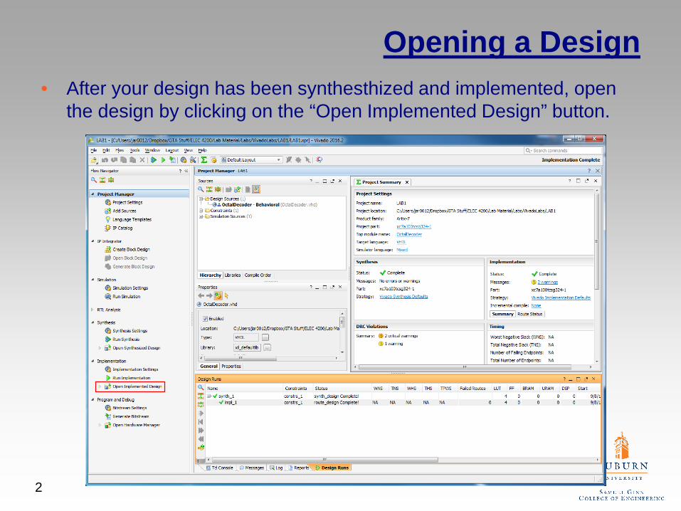
Opening a Design• After your design has been synthesthized and implemented, open
the design by clicking on the “Open Implemented Design” button.
2
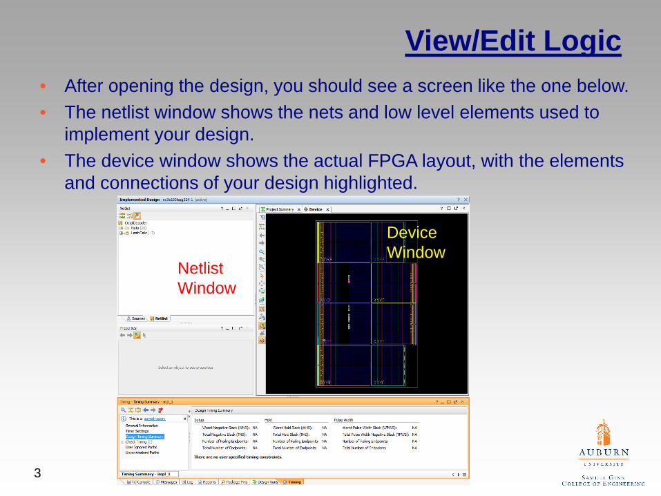
View/Edit Logic• After opening the design, you should see a screen like the one below.• The netlist window shows the nets and low level elements used to
implement your design.• The device window shows the actual FPGA layout, with the elements
and connections of your design highlighted.
3
NetlistWindow
DeviceWindow
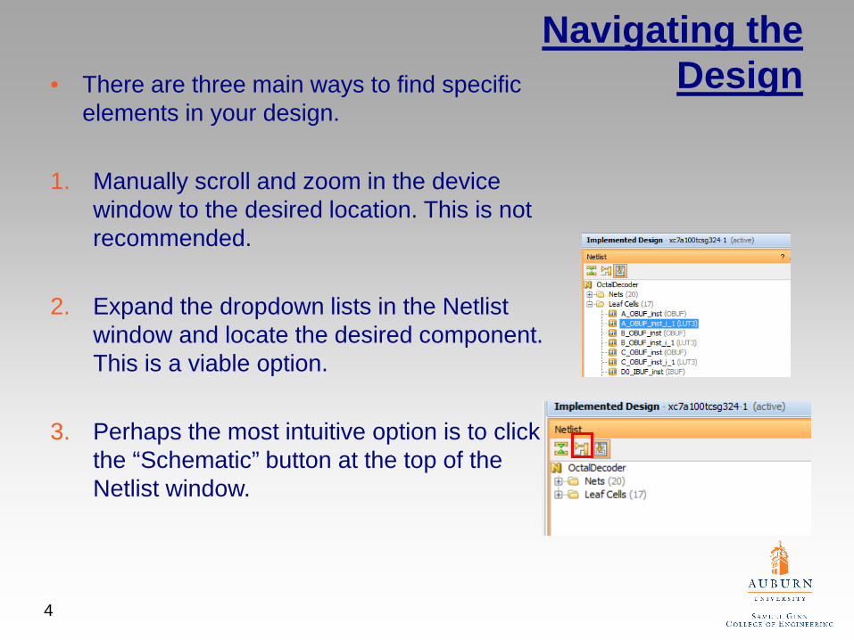
Navigating the Design• There are three main ways to find specific
elements in your design.
1. Manually scroll and zoom in the device window to the desired location. This is not recommended.
2. Expand the dropdown lists in the Netlist window and locate the desired component. This is a viable option.
3. Perhaps the most intuitive option is to click the “Schematic” button at the top of the Netlist window.
4

Viewing the Schematic• The schematic window shows
all the elements you had selected (by default this is all of them) and their interconnects.
• This schematic is from the octal to 7 segment decoder you designed in Lab 1.
• It should look similar to the gate level drawing you did for that prelab, except that AND/OR gates have been replaced with Look-Up-Tables (LUTs).
• You can also see I/O pins and buffers.
5
Exploring the Design
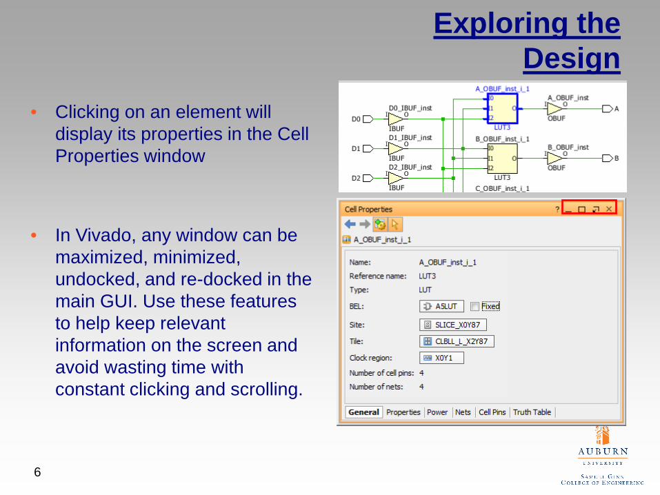
• Clicking on an element will display its properties in the Cell Properties window
• In Vivado, any window can be maximized, minimized, undocked, and re-docked in the main GUI. Use these features to help keep relevant information on the screen and avoid wasting time with constant clicking and scrolling.
6

Exploring the Design
• To view the logic function implemented by the LUT, click on the Truth Table tab.• You will see a truth table and the
logic expression implemented by the LUT.
• Note that I2,I1,I0 and O are internal names to the LUT.
• To compare these equations to the ones you derived by hand for Lab 1, click the Nets or Cell Pins tab, or look at the schematic, and record which internal name corresponds to which external name.
• For this LUT:• D2 ≡ I0• D1 ≡ I1• D0 ≡ I2• A ≡ O
7
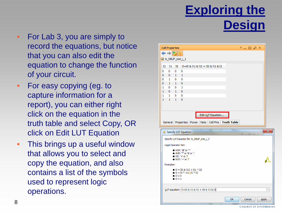
Exploring the Design
• For Lab 3, you are simply to record the equations, but notice that you can also edit the equation to change the function of your circuit.
• For easy copying (eg. to capture information for a report), you can either right click on the equation in the truth table and select Copy, OR click on Edit LUT Equation
• This brings up a useful window that allows you to select and copy the equation, and also contains a list of the symbols used to represent logic operations.
8
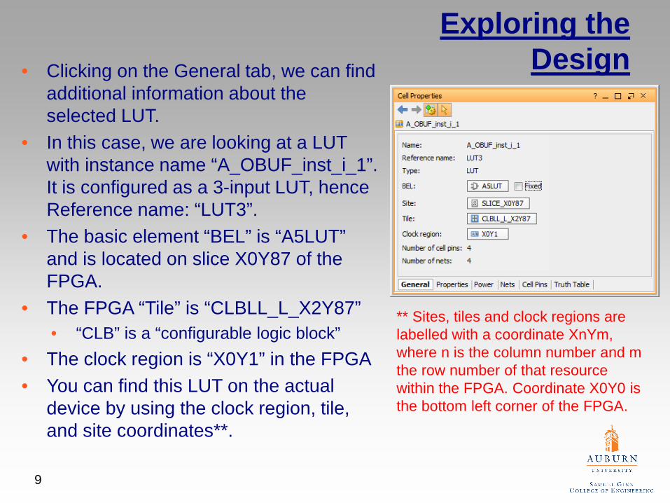
Exploring the Design• Clicking on the General tab, we can find
additional information about the selected LUT.
• In this case, we are looking at a LUT with instance name “A_OBUF_inst_i_1”. It is configured as a 3-input LUT, hence Reference name: “LUT3”.
• The basic element “BEL” is “A5LUT” and is located on slice X0Y87 of the FPGA.
• The FPGA “Tile” is “CLBLL_L_X2Y87”• “CLB” is a “configurable logic block”
• The clock region is “X0Y1” in the FPGA• You can find this LUT on the actual
device by using the clock region, tile, and site coordinates**.
9
** Sites, tiles and clock regions are labelled with a coordinate XnYm, where n is the column number and m the row number of that resource within the FPGA. Coordinate X0Y0 is the bottom left corner of the FPGA.
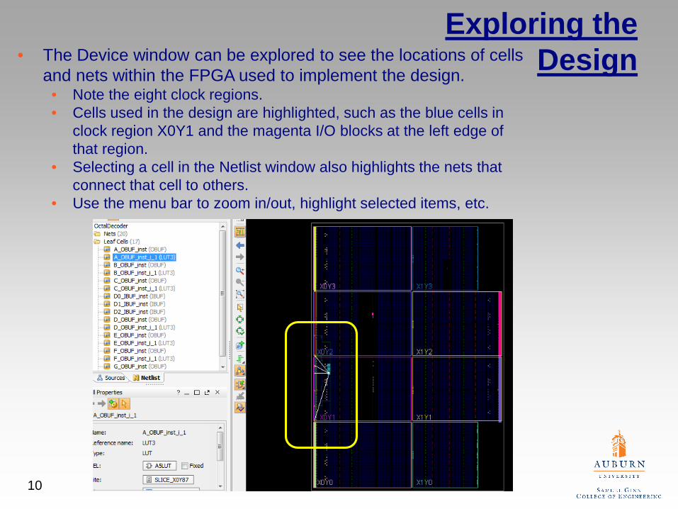
Exploring the Design• The Device window can be explored to see the locations of cells
and nets within the FPGA used to implement the design. • Note the eight clock regions.• Cells used in the design are highlighted, such as the blue cells in
clock region X0Y1 and the magenta I/O blocks at the left edge of that region.
• Selecting a cell in the Netlist window also highlights the nets that connect that cell to others.
• Use the menu bar to zoom in/out, highlight selected items, etc.
10
Exploring the Design
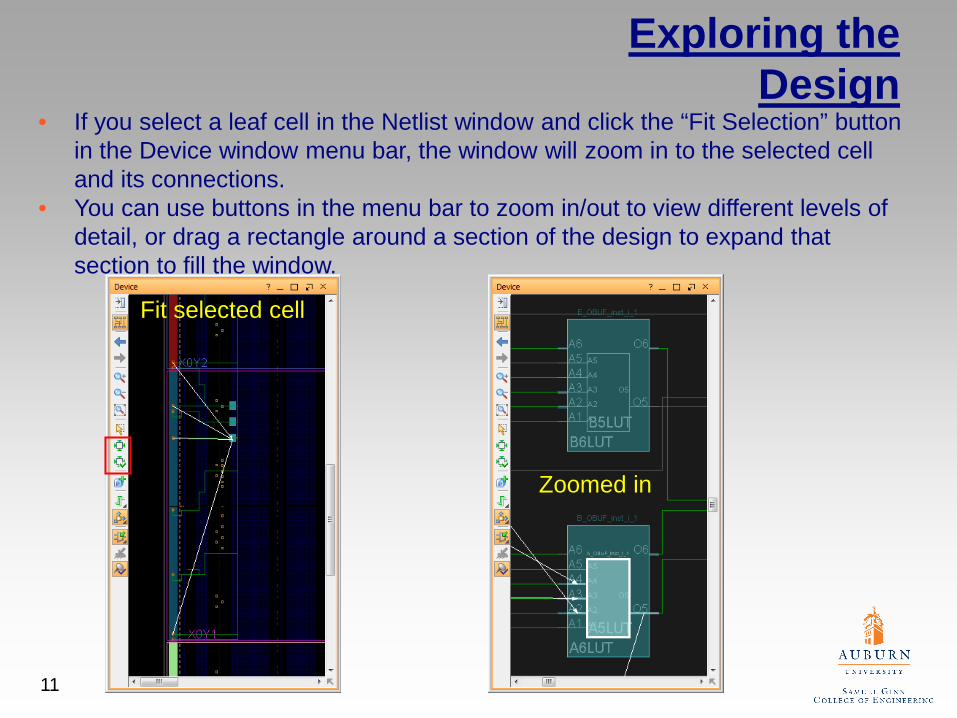
• If you select a leaf cell in the Netlist window and click the “Fit Selection” button in the Device window menu bar, the window will zoom in to the selected cell and its connections.
• You can use buttons in the menu bar to zoom in/out to view different levels of detail, or drag a rectangle around a section of the design to expand that section to fill the window.
11
Fit selected cell
Zoomed in

Exploring the Design
• Once you have found the desired correct slice, and you should notice several facts.
• First, there are only four LUTs present, not the seven shown on the schematic.
• Second, these are 6-input LUTs, not the 3-input LUTs in the schematic.
• You should spend some time exploring and try to understand why this might be. There is a question related to it in your lab manual.
12
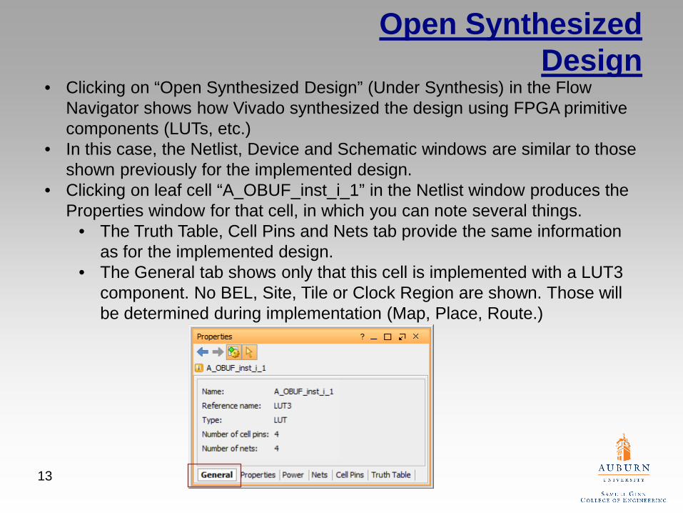
Open Synthesized Design
13
• Clicking on “Open Synthesized Design” (Under Synthesis) in the Flow Navigator shows how Vivado synthesized the design using FPGA primitive components (LUTs, etc.)
• In this case, the Netlist, Device and Schematic windows are similar to those shown previously for the implemented design.
• Clicking on leaf cell “A_OBUF_inst_i_1” in the Netlist window produces the Properties window for that cell, in which you can note several things.
• The Truth Table, Cell Pins and Nets tab provide the same information as for the implemented design.
• The General tab shows only that this cell is implemented with a LUT3 component. No BEL, Site, Tile or Clock Region are shown. Those will be determined during implementation (Map, Place, Route.)
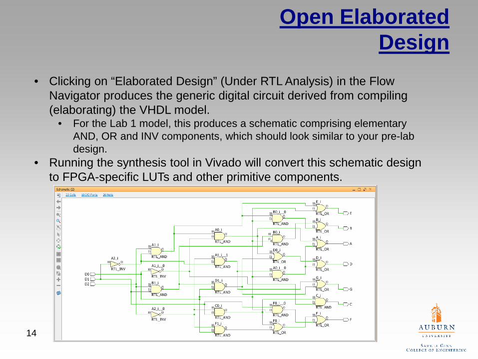
Open Elaborated Design
14
• Clicking on “Elaborated Design” (Under RTL Analysis) in the Flow Navigator produces the generic digital circuit derived from compiling (elaborating) the VHDL model.
• For the Lab 1 model, this produces a schematic comprising elementary AND, OR and INV components, which should look similar to your pre-lab design.
• Running the synthesis tool in Vivado will convert this schematic design to FPGA-specific LUTs and other primitive components.