· web viewloss due to leakage current during forward and reverse blocking. switching losses...
TRANSCRIPT
EE6303- POWER ELECTRONICS – QB 16marks
DEPARTMENT OF ELECTRICAL AND ELECTRONICS ENGINEERING
Question bank
EE6503-POWER ELECTRONICS
PART A
UNIT-I POWER SEMI-CONDUCTOR DEVICES
1. Why IGBT is very popular nowadays?
a. Lower hate requirements
b.Lower switching losses
c. Smaller snubbed circuit requirements
2. What are the different methods to turn on the thyristor?
a. Forward voltage triggering
b.Gate triggering
c. dv/dt triggering
d.Temperature triggering
e. Light triggering
3. What is the difference between power diode and signal diode?
Power diode Signal diode 1.Constructed with n-layer, called drift region between p+ layer and n+
layer.Drift region is not present. 2.The voltage, current and power ratings are higher.Lower3.Power
diodes operate at high speeds. Operates at higher switching speed.
4. IGBT is a voltage controlled device. Why?
Because the controlling parameter is gate-emitter voltage.
5. Power MOSFET is a voltage controlled device. Why?
Because the output (drain) current can be controlled by gate-source voltage.
6. Power BJT is a current controlled device. Why?
Because the output (collector) current can be controlled by base current.
7. What are the different types of power MOSFET?
a. N-channel MOSFET
b.P-channel MOSFET
8. How can a thyristor turned off?
A thyristor can be turned off by making the current flowing through it to zero.
9. Define latching current.
EE6303- POWER ELECTRONICS – QB 16marks
The latching current is defined as the minimum value of anode current which it must attain during
turn on process to maintain conduction when gate signal is removed.
10. Define holding current
The holding current is defined as the minimum value of anode current below which it must fall to
for turning off the thyristor.
11. What is a snubber circuit?
It consists of a series combination of a resistor and a capacitor in parallel with the thyristors. It is
mainly used for dv / dt protection.
12. What losses occur in a thyristor during working conditions?
a. Forward conduction losses
b.Loss due to leakage current during forward and reverse blocking.
c. Switching losses at turn-on and turn-off.
d.Gate triggering loss.
13.Define hard-driving or over-driving.
When gate current is several times higher than the minimum gate current required, a thyristor is said to
be hard-fired or over-driven. Hard-firing of a thyristor reduces its turn-on time and enhances its di/dt
capability.
14. Define circuit turn off time.
It is defined as the time during which a reverse voltage is applied across the thyristor during
its commutation process.
15. Why circuit turn off time should be greater than the thyristor turn-off time?
Circuit turn off time should be greater than the thyristor turn-off time for reliable turn-off,
otherwise the device may turn-on at an undesired instant, a process called commutation failure.
17. What is the turn-off time for converter grade SCRs and inverter grade SCRs?
Turn-off time for converter grade SCRs is 50 – 100 ms turn-off time for converter grade SCRs and
inverter grade SCRs and for inverter grade SCRs is 3 – 50 ms.
18. What are the advantages of GTO over SCR?()
a. Elimination of commutation of commutating components in forced commutation, resulting in
reduction in cost, weight and volume.
b. Reduction in acoustic noise and electromagnetic noise due to elimination of commutation
chokes.
c. Faster turn-off, permitting high switching frequencies.
d. Improved efficiency of the converters.
EE6303- POWER ELECTRONICS – QB 16marks
19. What is meant by phase controlled rectifier?
It converts fixed ac voltage into variable dc voltage.
20.Mention some of the applications of controlled rectifier.
a. Steel rolling mills, printing press, textile mills and paper mills employing dc motor drives.
b.DC traction
c. Electro chemical and electro-metallurgical process
d.Portable hand tool drives
e. Magnet power supplies
f. HVDC transmission system
21. State the advantages of IGBT over MOSFET
Smaller snubber circuit requirements
Lower switching losses
Lower gate requirements
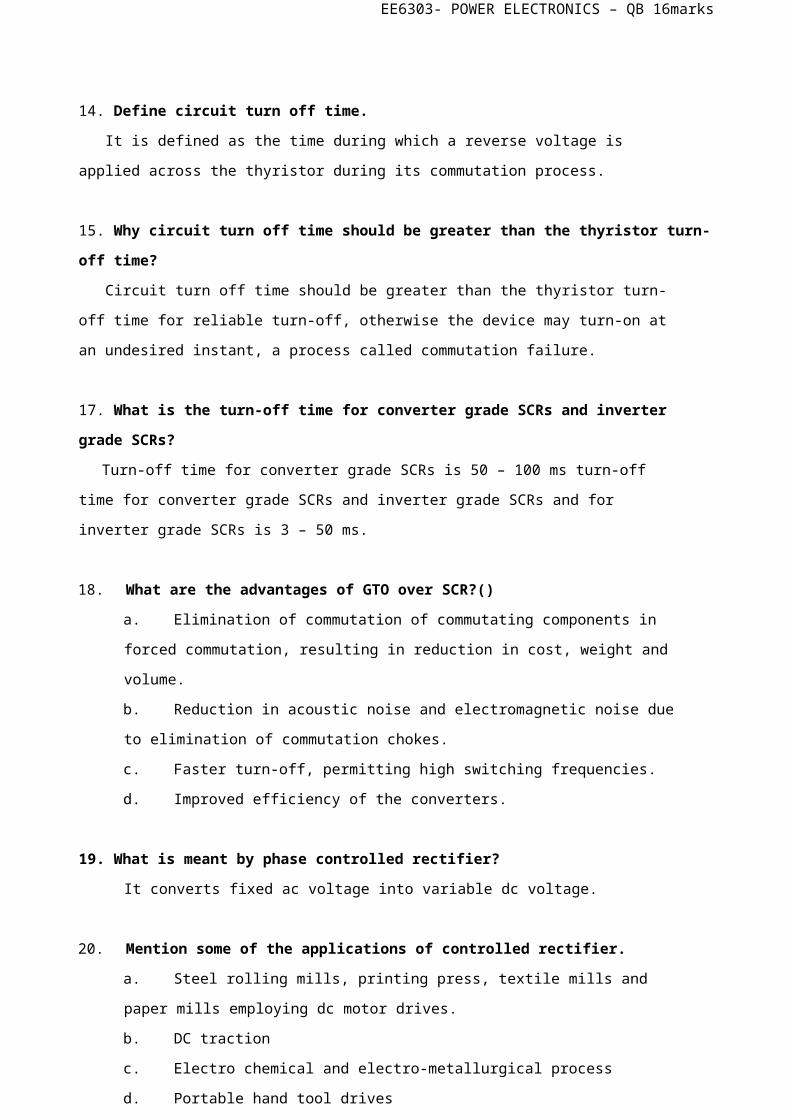
22. What are the applications of TRIAC
Fan regulators
Induction heating
AC voltage Regulators
Draw the turn on characteristics of TRIAC
UNIT-II
PHASE-CONTROLLED CONVERTERS
1. What is the function of freewheeling diodes in controlled rectifier?
It serves two process.
a. It prevents the output voltage from becoming negative.
b. The load current is transferred from the main thyristors to the freewheeling diode, thereby
allowing all of its thyristors to regain their blocking states.
2. What are the advantages of freewheeling diodes in a controlled in a controlled rectifier?
a. Input power factor is improved.
EE6303- POWER ELECTRONICS – QB 16marks
b.Load current waveform is improved and thus the load performance is better.
3. What is meant by delay angle?
The delay angle is defined as the angle between the zero crossing of the input voltage and the
instant the thyristors is fired.
4. What are the advantages of single phase bridge converter over single phase mid-point
converter?
a. SCRs are subjected to a peak-inverse voltage of 2Vm in a fully controlled bridge rectifier. Hence
for same voltage and current ratings of SCrs, power handled by mid-point configuration is about
b. In mid-point converter, each secondary winding should be able to supply the load power. As such,
the transformer rating in mid-point converter is double the load rating.
5. What is commutation angle or overlap angle?
The commutation period when outgoing and incoming thyristors are conducting isknown as
overlap period. The angular period, when both devices share conduction is known as the commutation
angle or overlap angle.
6. What are the different methods of firing circuits for line commutated converter?
a. UJT firing circuit.
b.The cosine wave crossing pulse timing control.
c. Digital firing schemes.
7. Give an expression for average voltage of single phase semiconverters.
Average output voltage Vdc = (Vm / _) (1 + cos _ ).
8. What is meant by input power factor in controlled rectifier?
The input power factor is defined as the ratio of the total mean input power to thetotal RMS
input volt-amperes.
PF = ( V1 I1 cos _1 ) / ( Vrms Irms) where V1 = phase voltage, I1 = fundamentalcomponent of the supply
current, _1 = input displacement angle, Irms = supply rms current.
9. What are the advantages of six pulse converter?
a. Commutation is made simple.
b. Distortion on the ac side is reduced due to the reduction in lower order harmonics.
c. Inductance reduced in series is considerably reduced.
10. What is meant by commutation?
It is the process of changing the direction of current flow in a particular path of the circuit. This
process is used in thyristors for turning it off.
EE6303- POWER ELECTRONICS – QB 16marks
11. What are the types of commutation?
a. Natural commutation
b.Forced commutation
12. What is meant by natural commutation?
Here the current flowing through the thyristor goes through a natural zero and enable the thyristor
to turn off.
13. What is meant by forced commutation?
In this commutation, the current flowing through the thyristor is forced to become zero by external
circuitry.
14. What is meant by dc chopper?
A dc chopper is a high speed static switch used to obtain variable dc voltage from a constant dc
voltage.
15.What are the applications of dc chopper?
a. Battery operated vehicles
b.Traction motor control in electric traction
c. Trolly cars
d.Marine hoists
e. Mine haulers
f. Electric braking.
16.What are the applications of dc chopper?
Chopper provides
a. High efficiency
b.Smooth acceleration
c. Fast dynamic response
d.Regeneration
17. What is meant by step-up and step-down chopper?
In a step- down chopper or Buck converter, the average output voltage is less than the input voltage. In a
step- up chopper or Boost converter, the average output voltage is more than the input voltage.
18.Write down the expression for average output voltage for step down chopper.
Average output voltage for step down chopper V0 = _ Vs, _ is the duty cycle
19.Write down the expression for average output voltage for step up chopper.
Average output voltage for step down chopper V0 = Vs, _ is the duty cycle
EE6303- POWER ELECTRONICS – QB 16marks
20. What is meant by duty-cycle?
Duty cycle is defined as the ratio of the on time of the chopper to the total time period of the
chopper. It is denoted by _.
UNIT-III
DC TO DC CONVERTER
1. What are the two types of control strategies?
a. Time Ratio Control (TRC)
b.Current Limit Control method (CLC)
2. What is meant by TRC?
In TRC, the value of Ton / T is varied in order to change the average output voltage.
3. What are the two types of TRC?
a. Constant frequency control
b.Variable frequency control
4. What is meant by FM control in a dc chopper?
In frequency modulation control, the chopping frequency f (or the chopping period T) is varied.
Here two controls are possible.
a. On-time Ton is kept constant
b. Off period Toff is kept constant.
5. What is meant by PWM control in dc chopper?
In this control method, the on time Ton is varied but chopping frequency is kept constant. The width
of the pulse is varied and hence this type of control is known as Pulse Width Modulation (PWM).
6. Write down the expression for the average output voltage for step down and step up chopper.
Average output voltage for step down chopper is VO = _ VS. Average output voltage for step
up chopper is VO = _ VS x [ ( 1- _ )]1/.
7. What are the different types of chopper with respect to commutation process?
a. Voltage commutated chopper.
b.Current commutated chopper.
c. Load commutated chopper.
8. What is meant by voltage commutation?
In this process, a charged capacitor momentarily reverse biases the conducting thyristor and
turn it off.
EE6303- POWER ELECTRONICS – QB 16marks
9. What is meant by current commutation?
In this process, a current pulse is made to flow in the reverse direction through the conducting
thyristor and when the net thyristor current becomes zero, it is turned off.
10. What is meant by load commutation?
In this process, the load current flowing through the thyristor either becomes zero or is transferred to
another device from the conducting thyristor.
11.What are the advantages of current commutated chopper?
a. The capacitor always remains charged with the correct polarity.
b. Commutation is reliable as load current is less than the peak commutation current ICP.
c. The auxiliary thyristor TA is naturally commutated as its current passes through zero value.
12.What are the advantages of load commutated chopper?
a. Commutating inductor is not required.
b. It is capable of commutating any amount of load current.
c. It can work at high frequencies in the order of kHz.
d.Filtering requirements are minimal.
13.What are the disadvantages of load commutated chopper?
a. For high power applications, efficiency becomes very low because of high switching losses
at high operating frequencies.
c. Peak load voltage is equal to twice the supply voltage.
d. The commutating capacitor has to carry full load current at a frequency of half chopping
frequency.
e. One thyristor pair should be turned-on only when the other pair is commutated. This can be
realized by sensing the capacitor current that is alternating.
14. What is meant by inverter?
A device that converts dc power into ac power at desired output voltage and frequency is called
an inverter.
15.What are the applications of an inverter?
a. Adjustable speed drives
b. Induction heating
c. Stand-by aircraft power supplies
d.UPS
e. HVDC transmission
16.What are the main classification of inverter?
EE6303- POWER ELECTRONICS – QB 16marks
a. Voltage Source Inverter
b.Current Source Inverter
17.Why thyristors are not preferred for inverters?
Thyristors require extra commutation circuits for turn off which results in increased complexity of the
circuit. For these reasons thyristors are not preferred for inverters.
18. How output frequency is varied in case of a thyristor?
The output frequency is varied by varying the turn off time of the thyristors in the inverter circuit,
i.e. the delay angle of the thyristors is varied.
19.Give two advantages of CSI.
a. CSI does not require any feedback diodes.
b.Commutation circuit is simple as it involves only thyristors.
20.What is the main drawback of a single phase half bridge inverter?
It require a 3-wire dc supply.
UNIT-IV
INVERTERS
1. Why diodes should be connected in antiparallel with the thyristors in inverter circuits?
For RL loads, load current will not be in phase with load voltage and the diodes connected in anti
parallel will allow the current to flow when the main thyristors are turned off. These diodes are called
feedback diodes.
2. What types of inverters require feedback diodes?
VSI with RL load.
3. What is meant a series inverter?
An inverter in which the commutating elements are connected in series with the load is called a
series inverter.
4. What is the condition to be satisfied in the selection of L and C in a series inverter?
R2 < 4L
5. What is meant a parallel inverter?
EE6303- POWER ELECTRONICS – QB 16marks
An inverter in which the commutating elements are connected in parallel with the load is called a
parallel inverter.
6. What are the applications of a series inverter?
The thyristorised series inverter produces an approximately sinusoidal waveform at a high output
frequency, ranging from 200 Hz to 100kHz. It is commonly used for fixed output applications such as
a. Ultrasonic generator.
b. Induction heating.
c. Sonar Transmitter
d.Fluorescent lighting.
7. How is the inverter circuit classified based on commutation circuitry?
b.Load commutated inverters.
c. Self commutated inverters.
d.Forced commutated inverters.
8. What is meant by McMurray inverter?
It is an impulse commutated inverter which relies on LC circuit and an auxiliary thyristor for
commutation in the load circuit.
9. What are the applications of a CSI?
a. Induction heating
b.Lagging VAR compensation
c. Speed control of ac motors
d.Synchronous motor starting.
10.What is meant by PWM control?
In this method, a fixed dc input voltage is given to the inverter and a controlled ac output
voltage is obtained by adjusting the on and off periods of the inverter
components. This is the most popular method of controlling the output voltage and this method is
termed as PWM control
.
11.What are the advantages of PWM control?
a. The output voltage can be obtained without any additional components.
b. Lower order harmonics can be eliminated or minimized along with its output voltage control.
As the higher order harmonics can be filtered easily, the filtering requirements are minimized.
12.What are the disadvantages of the harmonics present in the inverter system?
a. Harmonic currents will lead to excessive heating in the induction motors. This will reduce the
load carrying capacity of the motor.

EE6303- POWER ELECTRONICS – QB 16marks
b. If the control and the regulating circuits are not properly shielded, harmonics from power ride
can affect their operation and malfunctioning can result.
c. Harmonic currents cause losses in the ac system and can even some time produce resonance in the
system. Under resonant conditions, the instrumentation and metering can be affected.
d. On critical loads, torque pulsation produced by the harmonic current can be useful.
13.What are the methods of reduction of harmonic content?
a. Transformer connections
b.Sinusoidal PWM
c. Multiple commutation in each cycle
d.Stepped wave inverters
14.Compare CSI and VSI.
1.Input voltage is maintained Constant Input current is constant but adjustable
2.The output voltage does not depend on the load The output current does not depend on the load
3.The magnitude of the output current and its waveform depends on the nature of the load
impedance The magnitude of the output voltage
and its waveform depends on the nature of the load impedance 4.It requires feedback
diodes It does not requires feedback diodes
5. Commutation circuit is complicated i.e. it contains capacitors and inductors. Commutation
circuit is simple i.e. it contains only capacitors.
15. What are the disadvantages of PWM control?
SCRs are expensive as they must possess low turn-on and turn-off times.
16. What does ac voltage controller mean?
It is device which converts fixed alternating voltage into a variable voltage without change in
frequency.
17.What are the applications of ac voltage controllers?
a. Domestic and industrial heating
b.Lighting control
c. Speed control of single phase and three phase ac motors
d.Transformer tap changing
18.What are the advantages of ac voltage controllers?
a. High efficiency
b.Flexibility in control
c. Less maintenance
EE6303- POWER ELECTRONICS – QB 16marks
19.What are the disadvantages of ac voltage controllers?
The main draw back is the introduction of harmonics in the supply current and the load voltage
waveforms particularly at low output voltages
.
20.What are the two methods of control in ac voltage controllers?
a. ON-OFF control
b.Phase control
UNIT-V
AC TO AC CONVERTERS
1. What is the difference between ON-OFF control and phase control?
ON-OFF control: In this method, the thyristors are employed as switches to connect the load circuit to
the source for a few cycles of the load voltage and disconnect it for another few cycles. Phase control: In
this method, thyristor switches connect the load to the ac source for a portion of each half cycle of input
voltage.
2. What is the advantage of ON-OFF control?
Due to zero-voltage and zero current switching of thyristors, the harmonics generated by the
switching action are reduced.
3. What is the disadvantage of ON-OFF control?
This type of control is applicable in systems that have high mechanical inertia and high thermal time
constant.
4. What is the duty cycle in ON-OFF control method?
Duty cycle K = n/ (n + m), where n = no. of ON cycles, m = no. of OFF cycles.
5. What is meant by unidirectional or half-wave ac voltage controller?
Here the power flow is controlled only during the positive half-cycle of the input voltage.
6. What are the disadvantages of unidirectional or half-wave ac voltage controller?
a. Due to the presence of diode on the circuit, the control range is limited and the effective RMS
output voltage can be varied between 70.7% and 100%.
b. The input current and output voltage are asymmetrical and contain a dc component. If there
is an input transformer, saturation problem will occur
c. It is only used for low power resistive load.
7. What is meant by bidirectional or half-wave ac voltage controller?
EE6303- POWER ELECTRONICS – QB 16marks
Here the power flow is controlled during both cycles of the input voltage.
8. What is the control range of firing angle in ac voltage controller with RL load?
9. What type of gating signal is used in single phase ac voltage controller with RL load?
High frequency carrier gating signal is used for single phase ac voltage controller with RL load.
10.What are the disadvantages of continuous gating signal?
a. More heating of the SCR gate.
b. Increases the size of pulse transformer.
11. What is meant by high frequency carrier gating?
Thyristor is turned on by using a train of pulses from a to p. This type of signal is called as high
frequency carrier gating.
12. What is meant by sequence control of ac voltage regulators?
It means that the stages of voltage controllers in parallel triggered in a proper sequence one after the
other so as to obtain a variable output with low harmonic content.
13. What are the advantages of sequence control of ac voltage regulators?
a. System power factor is improved.
b.Harmonics are reduced in the source current and the load voltage.
14.What is meant by cyclo-converter?
It converts input power at one frequency to output power at another frequency with one-stage
conversion. Cycloconverter is also known as frequency changer.
15.What are the two types of cyclo-converters?
a. Step-up cyclo-converters
b.Step-down cyclo-converters
16.What is meant by step-up cyclo-converters?
In these converters, the output frequency is less than the supply frequency.
17. What is meant by step-down cyclo-converters?
In these converters, the output frequency is more than the supply frequency.
18.What are the applications of cyclo-converter?
a. Induction heating
b.Speed control of high power ac drives
d.Power supply in aircraft or ship boards
EE6303- POWER ELECTRONICS – QB 16marks
19.What is meant by positive converter group in a cyclo converter?
The part of the cycloconverter circuit that permits the flow of current during Positive half cycle
of output current is called positive converter group.
20. What is meant by negative converter group in a cyclo converter?
The part of the cyclo converter circuit that permits the flow of current during negative half cycle
of output current is called negative converter group.
POWER ELECTRONICS
PART B
Unit I
Power Semiconductor Devices
1. Briefly explain the structure and VI characteristics of Power DiodePower diode:
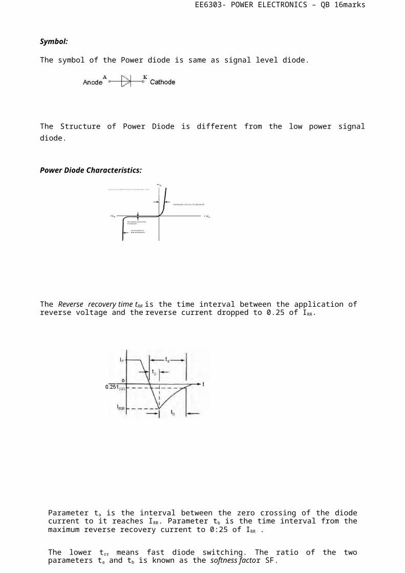
Diode is a two terminal P-N junction semiconductor device, with terminals anode (A) and cathode (C).
Symbol:
The symbol of the Power diode is same as signal level diode.
The Structure of Power Diode is different from the low power signal diode.
Power Diode Characteristics:
The Reverse recovery time tRR is the time interval between the application of reverse voltage and the reverse current dropped to 0.25 of IRR.
EE6303- POWER ELECTRONICS – QB 16marks
Parameter ta is the interval between the zero crossing of the diode current to it reaches IRR. Parameter tb is the time interval from the maximum reverse recovery current to 0:25 of IRR .
The lower trr means fast diode switching. The ratio of the two parameters ta and tb is known as the softness factor SF.
Power Diode Applications:
As a rectifier Diode
For Voltage Clamping
As a Voltage Multiplier
As a freewheeling Diode
Types of Diodes
Schottky diodes:
These diodes are used where a low forward voltage drop (usually 0.3V) is needed in low output voltage circuits. These diodes are limited in their blocking voltage capabilities to 50 – 100V.
Fast Recovery diodes:
These are used in high frequency circuits in combination with controllable switches where a small reverse recovery time is needed. At power levels of several hundred volts and several hundred amperes, these diodes have trr ratings of less than a few microsecond.
Line frequency diodes:
The on state voltage of these diodes is designed to be as low as possible and as a consequence have larger trr, which are acceptable for line frequency applications. These diodes are available with blocking voltage ratings of several kilovolts and current ratings of several kilo amperes. Moreover, they can be connected in series and parallel to satisfy any voltage and current requirement.
EE6303- POWER ELECTRONICS – QB 16marks
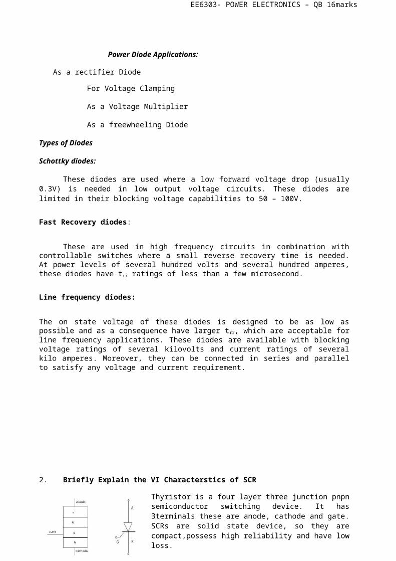
2. Briefly Explain the VI Characterstics of SCR
Thyristor is a four layer three junction pnpn semiconductor switching device. It has 3terminals these are anode, cathode and gate. SCRs are solid state device, so they are compact,possess high reliability
and have low loss.
SCR is made up of silicon, it act as a rectifier; it has very low resistance in the forwarddirection and high resistance in the reverse direction. It is a unidirectional device.
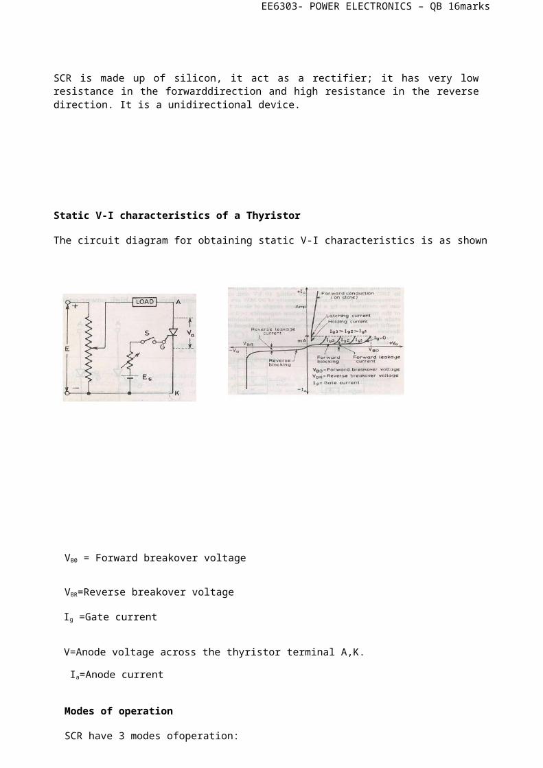
Static V-I characteristics of a Thyristor
The circuit diagram for obtaining static V-I characteristics is as shown
VB0 = Forward breakover voltage

EE6303- POWER ELECTRONICS – QB 16marks
VBR=Reverse breakover voltage
Ig =Gate current
V=Anode voltage across the thyristor terminal A,K.
Ia=Anode current
Modes of operation
SCR have 3 modes ofoperation:
Reverse blocking mode Forward blocking mode ( off state) Forward conduction mode (on state)
3. Briefly explain the Turn ON methods of SCRDifferent turn ON methods for SCR
1. Forward voltage triggering2. Gate triggering
3. / triggering
4. Light triggering
5. Temperature triggering
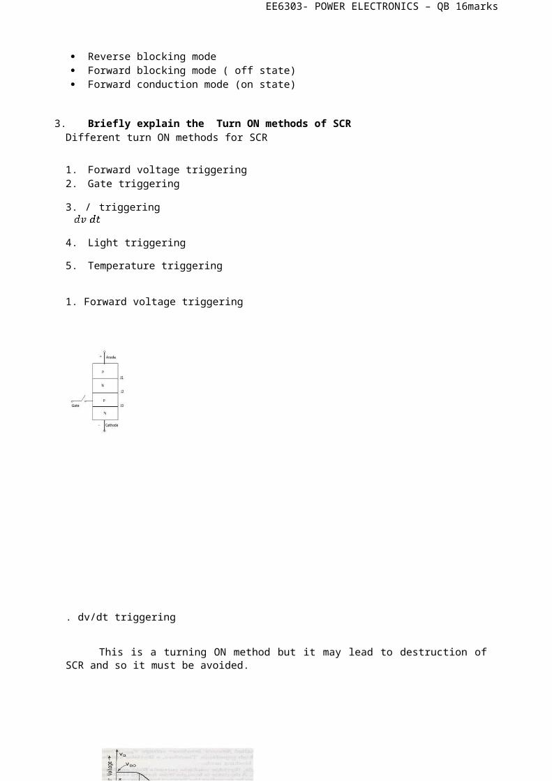
1. Forward voltage triggering
. dv/dt triggering
EE6303- POWER ELECTRONICS – QB 16marks
This is a turning ON method but it may lead to destruction of SCR and so it must be avoided.
Latching current
The latching current may be defined as the minimum value of anode current which at must attain during turn ON process to maintain conduction even if gate signal is removed.
Holding current
It is the minimum value of anode current below which if it falls, the SCR will turn OFF.
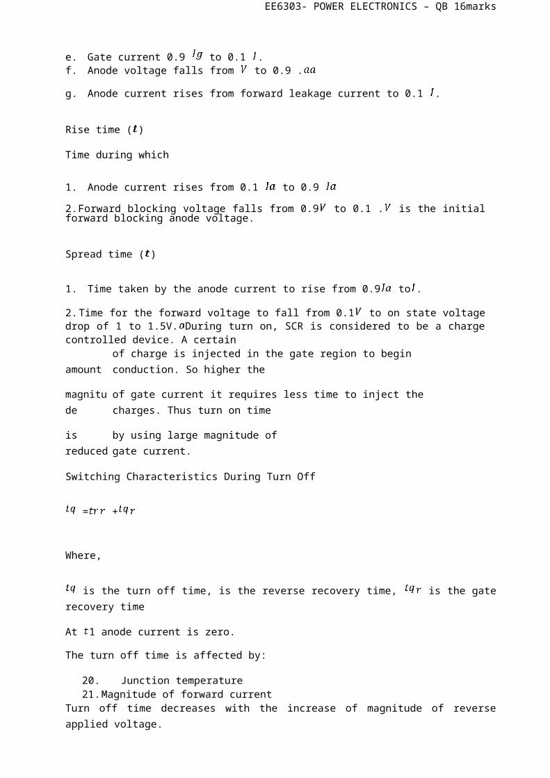
4. Briefly explain the Switching characteristics of thyristors
It is the time during which it changes from forward blocking state to ON state. Total turnon time is divided into 3 intervals:
1. Delay time2. Rise time3. Spread time
Delay time
If and represent the final value of gate current and anode current. Then the
delay timecan be explained as time during which the gate current attains 0.9 to the
EE6303- POWER ELECTRONICS – QB 16marks
instant anodecurrent reaches 0.1 or the anode current rises from forward leakage current to 0.1 .
e. Gate current 0.9 to 0.1 .f. Anode voltage falls from to 0.9 .
g. Anode current rises from forward leakage current to 0.1 .
Rise time ( )
Time during which
1. Anode current rises from 0.1 to 0.9
2. Forward blocking voltage falls from 0.9 to 0.1 . is the initial forward blocking anode voltage.
Spread time ( )
1. Time taken by the anode current to rise from 0.9 to .
2. Time for the forward voltage to fall from 0.1 to on state voltage drop of 1 to 1.5V. During turn on, SCR is considered to be a charge controlled device. A certainamount of charge is injected in the gate region to begin conduction. So higher the
magnitude of gate current it requires less time to inject the charges. Thus turn on time
is reduced by using large magnitude of gate current.
Switching Characteristics During Turn Off
= +
Where,
is the turn off time, is the reverse recovery time, is the gate recovery time
At 1 anode current is zero.
The turn off time is affected by:
20. Junction temperature21. Magnitude of forward current
Turn off time decreases with the increase of magnitude of reverse applied voltage.
EE6303- POWER ELECTRONICS – QB 16marks
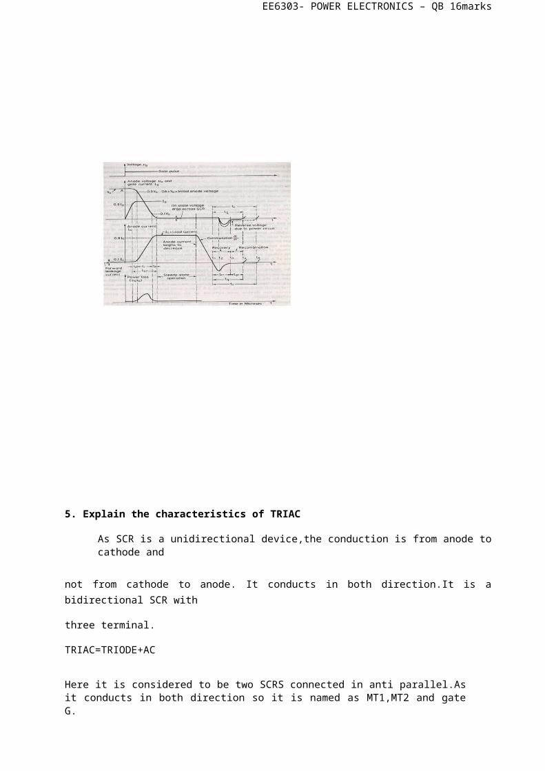
5. Explain the characteristics of TRIAC
As SCR is a unidirectional device,the conduction is from anode to cathode and
not from cathode to anode. It conducts in both direction.It is a bidirectional SCR with
three terminal.
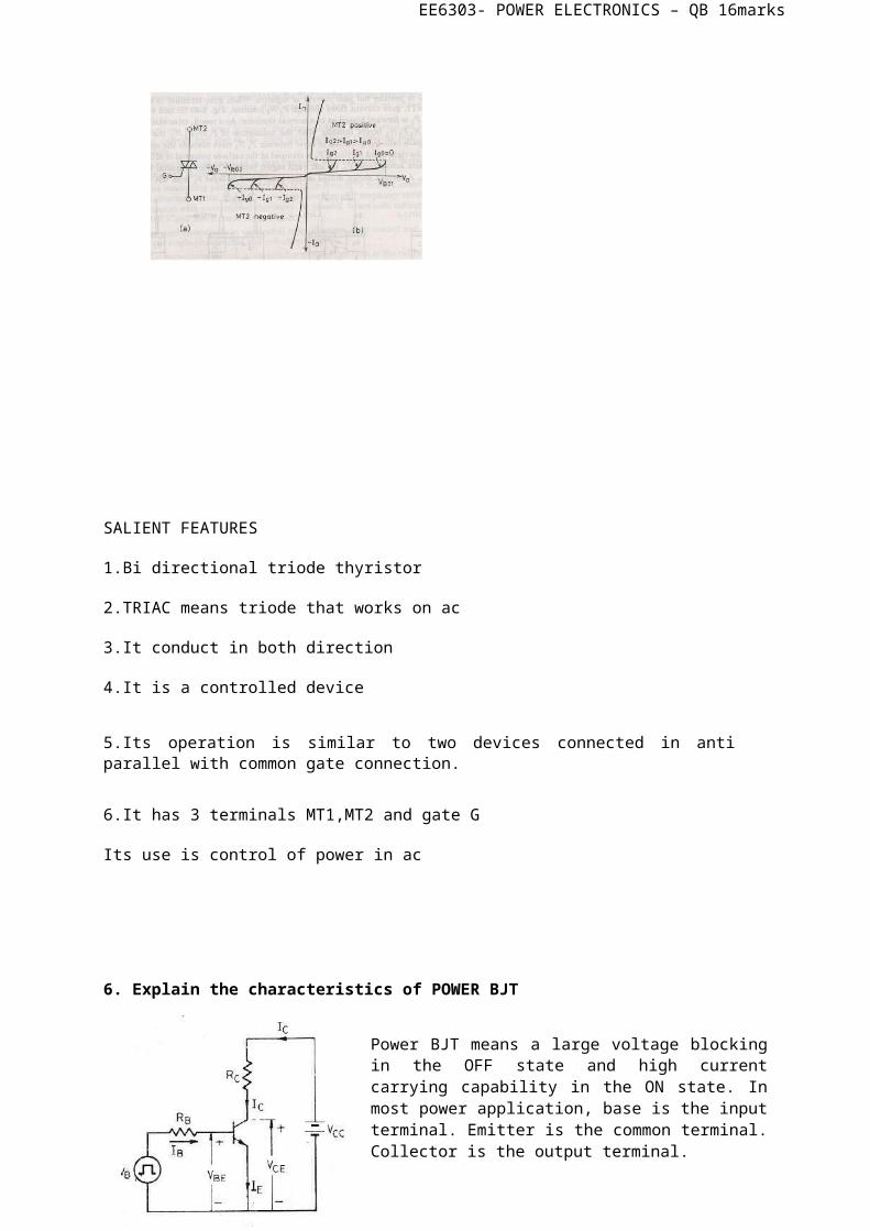
TRIAC=TRIODE+AC
Here it is considered to be two SCRS connected in anti parallel.As it conducts in both direction so it is named as MT1,MT2 and gate G.
EE6303- POWER ELECTRONICS – QB 16marks
SALIENT FEATURES
1.Bi directional triode thyristor
2.TRIAC means triode that works on ac
3.It conduct in both direction
4.It is a controlled device
5.Its operation is similar to two devices connected in anti parallel with common gate connection.
6.It has 3 terminals MT1,MT2 and gate G
Its use is control of power in ac
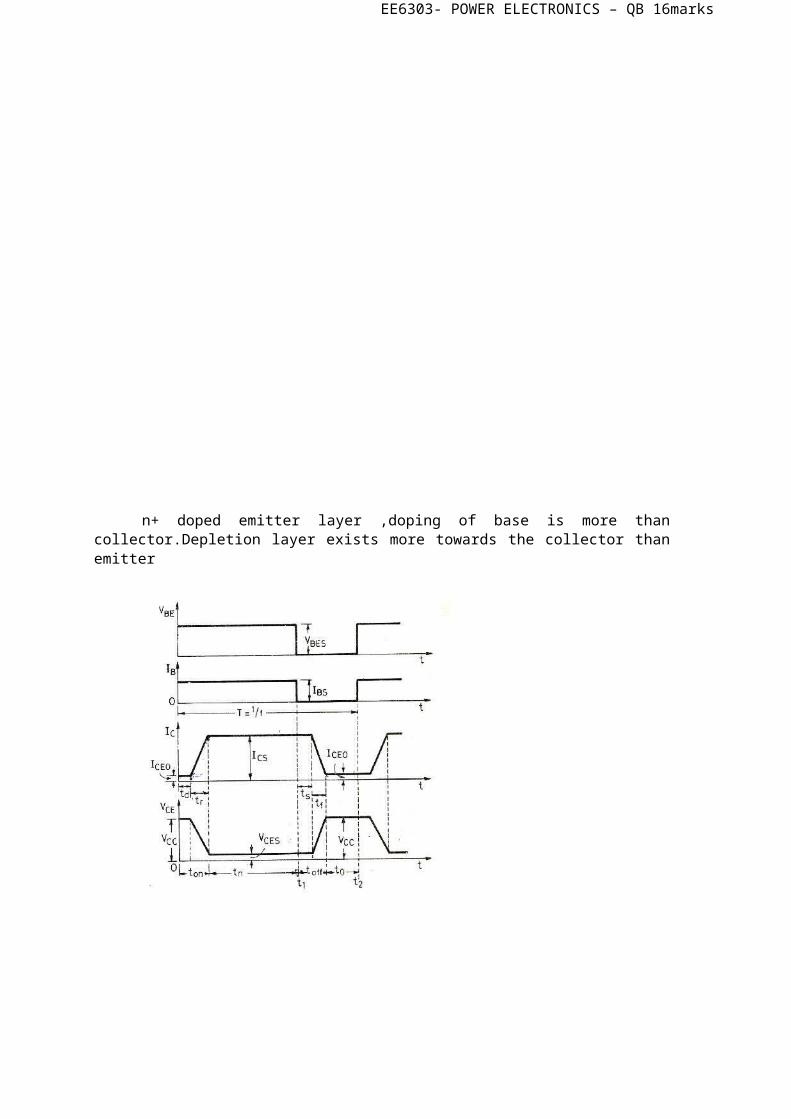
6. Explain the characteristics of POWER BJT
Power BJT means a large voltage blocking in the OFF state and high current carrying capability in the ON state. In most power application, base is the input terminal. Emitter is the common terminal. Collector is the output terminal.
EE6303- POWER ELECTRONICS – QB 16marks
n+ doped emitter layer ,doping of base is more than collector.Depletion layer exists more towards the collector than emitter
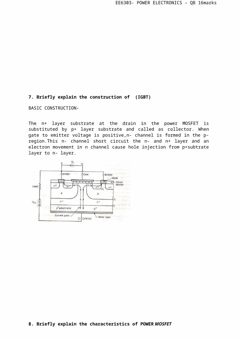
7. Briefly explain the construction of (IGBT)
BASIC CONSTRUCTION-
The n+ layer substrate at the drain in the power MOSFET is substituted by p+ layer substrate and called as collector. When gate to emitter voltage is positive,n- channel is formed in the p- region.This n- channel short circuit the n- and n+ layer and an electron movement in n channel cause hole injection from p+subtrate layer to n- layer.
EE6303- POWER ELECTRONICS – QB 16marks
8. Briefly explain the characteristics of POWER MOSFET
A power MOSFET has three terminal devices. Arrow indicates the direction of current flow. MOSFET is a voltage controlled device. The operation of MOSFET depends on flow of majority carriers only.
EE6303- POWER ELECTRONICS – QB 16marks
Switching Characteristics:-
The switching characteristic is influenced by
1. Internal capacitance of the device.
2. Internal impedance of the gate drive circuit. Total turn on time is divided into
1.Turn on delay time
2.Rise time
Switching waveform of power MOSFET
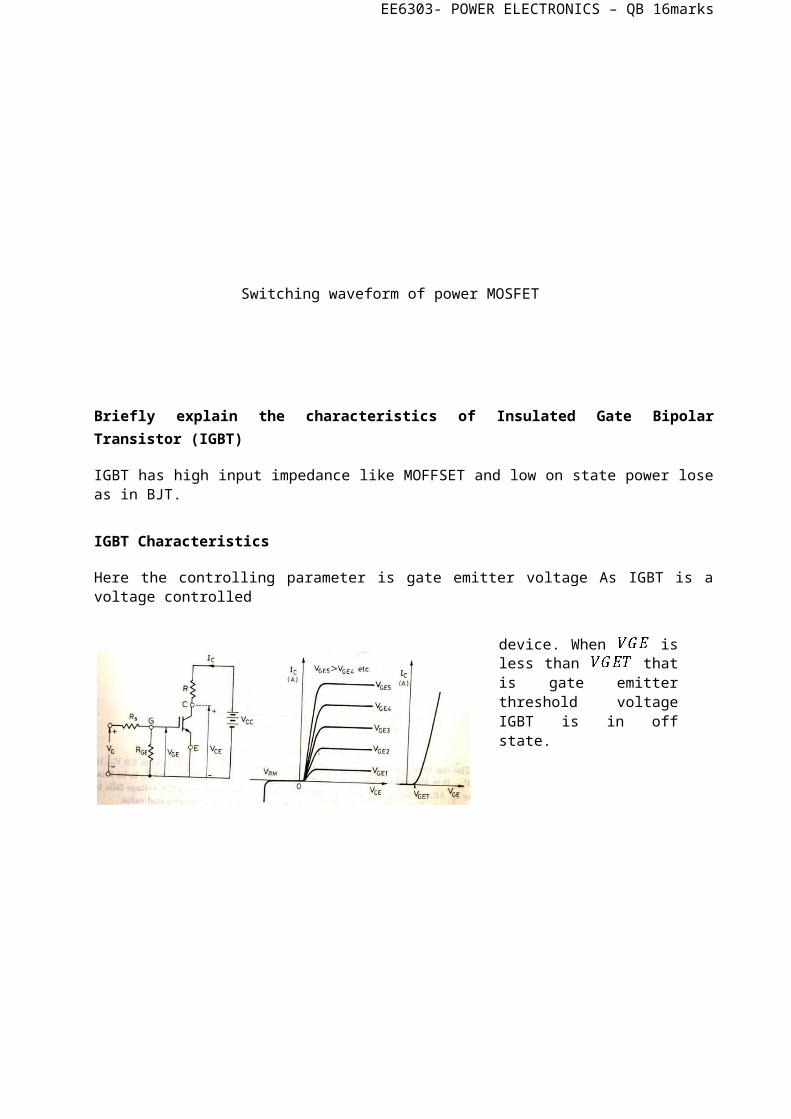
Briefly explain the characteristics of Insulated Gate Bipolar Transistor (IGBT)
IGBT has high input impedance like MOFFSET and low on state power lose as in BJT.
IGBT Characteristics
Here the controlling parameter is gate emitter voltage As IGBT is a voltage controlled
EE6303- POWER ELECTRONICS – QB 16marks
device. When is less than that is gate emitter threshold voltage IGBT is in off state.
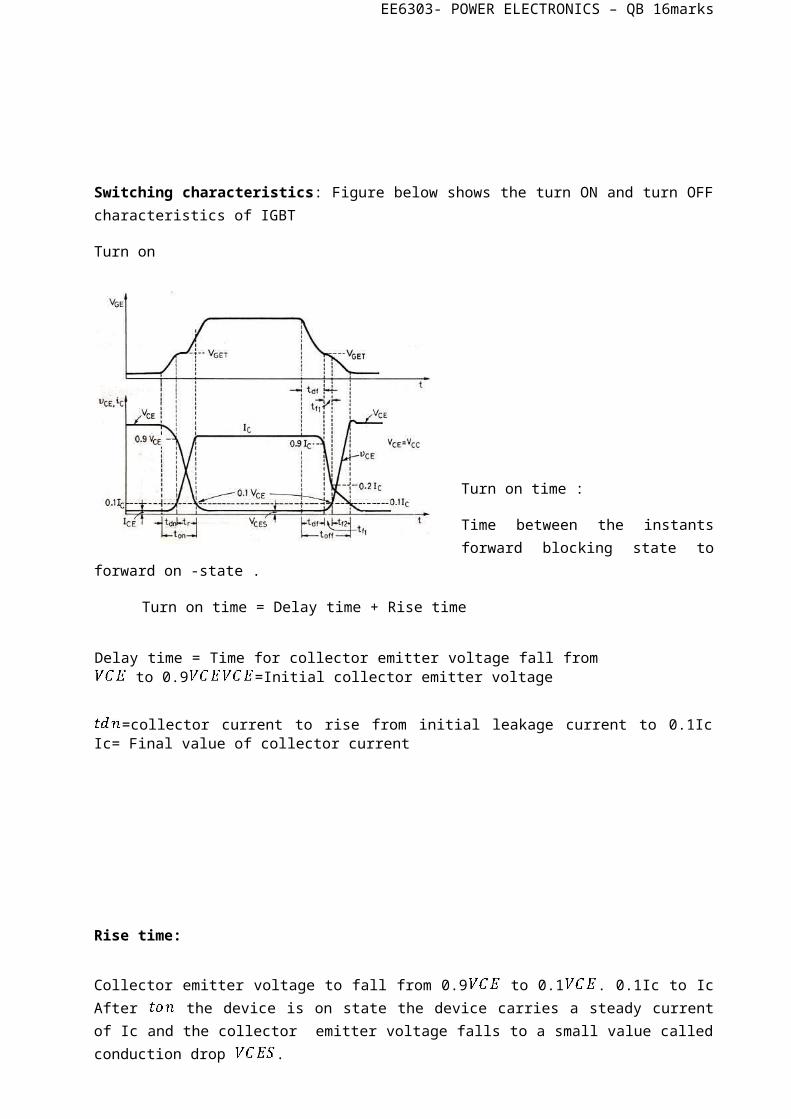
Switching characteristics: Figure below shows the turn ON and turn OFF characteristics of IGBT
Turn on
Turn on time :
Time between the instants forward blocking state to forward on -state .
Turn on time = Delay time + Rise time
Delay time = Time for collector emitter voltage fall from to 0.9=Initial collector emitter voltage
=collector current to rise from initial leakage current to 0.1Ic Ic= Final value of collector current
EE6303- POWER ELECTRONICS – QB 16marks
Rise time:
Collector emitter voltage to fall from 0.9 to 0.1 . 0.1Ic to Ic After the device is on state the device carries a steady current of Ic and the collector emitter voltage falls to a small value called conduction drop .
Turn off time :
5. Delay time
6. Initial fall time 1
7. Final fall time 2 =+ 1+ 2
= Time during which the gate emitter voltage falls to the threshold value .
Collector current falls from Ic to 0.9Ic at the end of the collector emitter voltage begins to rise. Turn off time = Collector current falls from 90% to 20% of its initial
value Ic OR The time during which collector emitter voltage rise from to 0.1 . 2=collector current falls from20% to 10% of Ic. During this collector emitter voltage
rise 0.1 to final value of .
UNIT II
PHASE-CONTROLLED CONVERTERS
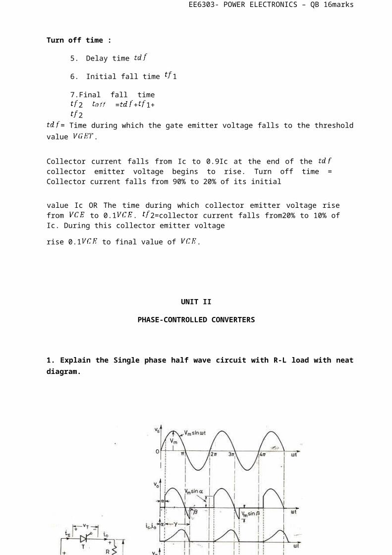
1. Explain the Single phase half wave circuit with R-L load with neat diagram.
EE6303- POWER ELECTRONICS – QB 16marks
EE6303- POWER ELECTRONICS – QB 16marks

EE6303- POWER ELECTRONICS – QB 16marks
EE6303- POWER ELECTRONICS – QB 16marks
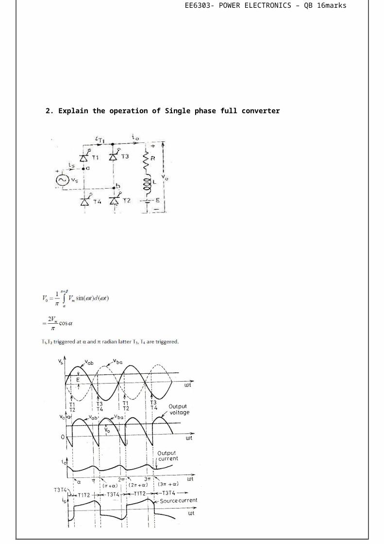
2. Explain the operation of Single phase full converter
EE6303- POWER ELECTRONICS – QB 16marks
EE6303- POWER ELECTRONICS – QB 16marks
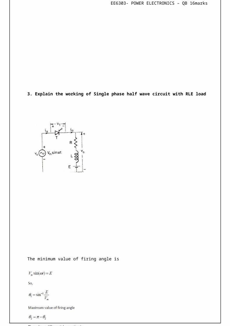
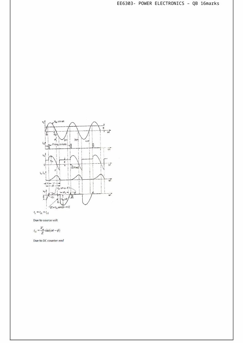
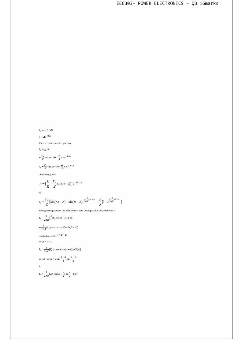
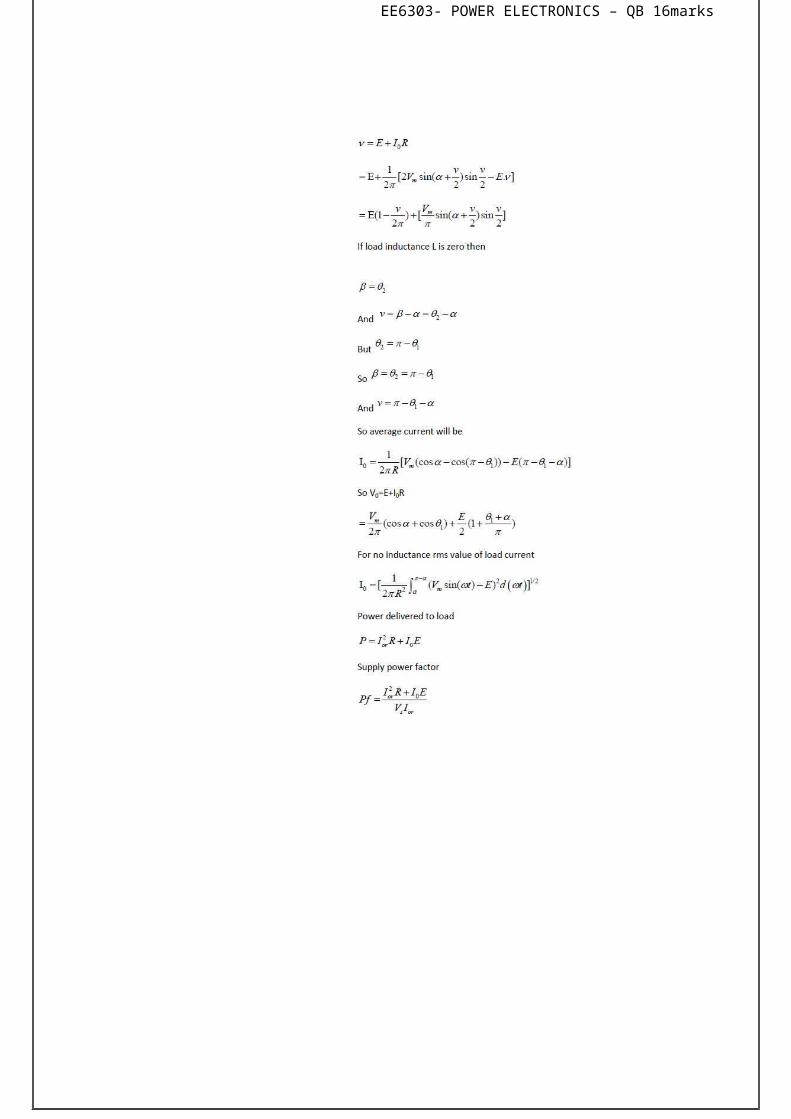
3. Explain the working of Single phase half wave circuit with RLE load
The minimum value of firing angle is

EE6303- POWER ELECTRONICS – QB 16marks
EE6303- POWER ELECTRONICS – QB 16marks
EE6303- POWER ELECTRONICS – QB 16marks
EE6303- POWER ELECTRONICS – QB 16marks
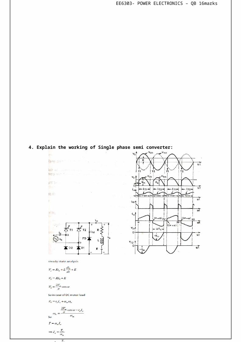
4. Explain the working of Single phase semi converter:

EE6303- POWER ELECTRONICS – QB 16marks
EE6303- POWER ELECTRONICS – QB 16marks
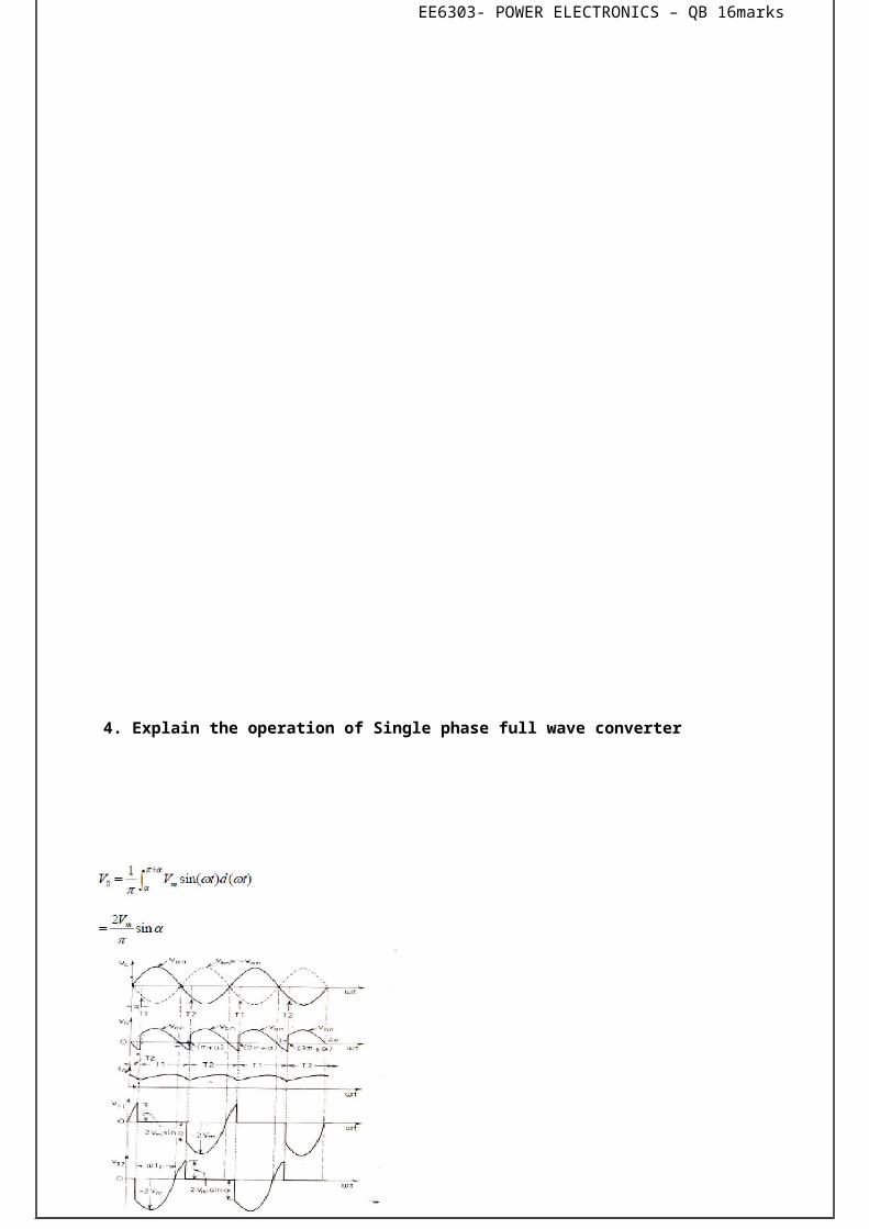
4. Explain the operation of Single phase full wave converter
EE6303- POWER ELECTRONICS – QB 16marks
1. Rectification:
The conversion of ac to dc is known as rectification.
2. Semi-converters:
It combines the features of both controlled rectifiers (using SCR) and uncontrolled rectifiers (using
diodes). The polarity of output voltage can be either positive ornegative.
3. Commutation:
It is the process of turning-off of a power semiconductor device.
4. Freewheeling diode:
A power diode connected parallel across the load to prevent the reversal of load voltage in order to
improve the input power factor.
5. Ripple:
EE6303- POWER ELECTRONICS – QB 16marks
AC component present in the DC output voltage.
6. Delay angle:
It is defined as the angle between the zero crossing of the input voltage and the instant the thyristors
is fired.
7. Overlap period:
The period during which both the incoming and outgoing thyristors conducts simultaneously is called
overlap period.
8. Overlap angle/ commutation angle:
The angle for which both devices share conduction is known as overlap angle.
9. Input Displacement Angle:
It is the angular displacement between the fundamental component current to the line to neutral
voltage of the input ac source.
10. Displacement factor:
It is defined as the cosine of the input displacement angle.
11. Distortion factor:
It is defined as the ratio of RMS amplitude of the fundamental component to the total RMS
amplitude.
12. Harmonic Factor:
EE6303- POWER ELECTRONICS – QB 16marks
It is defined as the ratio of the total harmonic content to the fundamental component.
EE6303- POWER ELECTRONICS – QB 16marks
UNIT III
DC TO DC CONVERTER
1 Explain the working principle of step down chopper
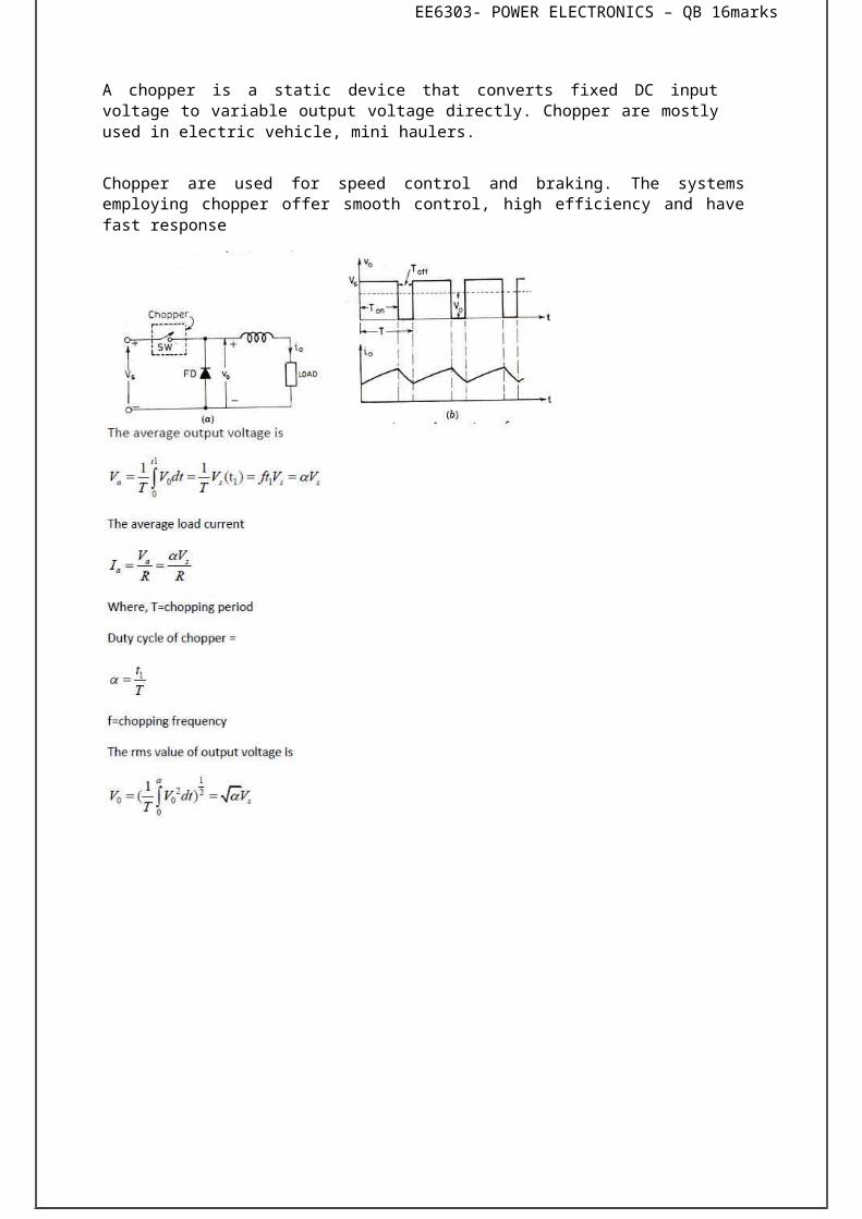
A chopper is a static device that converts fixed DC input voltage to variable output voltage directly. Chopper are mostly used in electric vehicle, mini haulers.
Chopper are used for speed control and braking. The systems employing chopper offer smooth control, high efficiency and have fast response

EE6303- POWER ELECTRONICS – QB 16marks
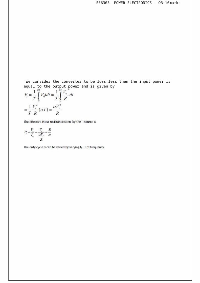
we consider the converter to be loss less then the input power is equal to the output power and is given by
EE6303- POWER ELECTRONICS – QB 16marks
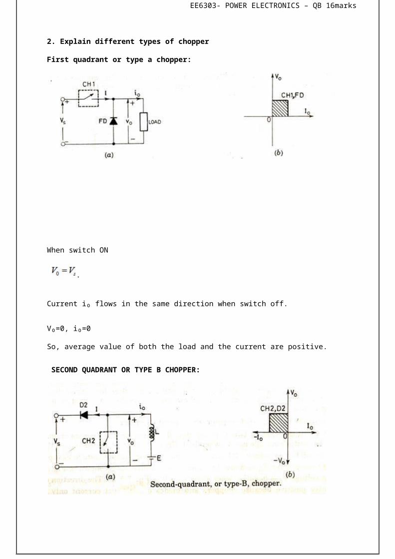
2. Explain different types of chopper
First quadrant or type a chopper:
When switch ON
Current i₀ flows in the same direction when switch off.

EE6303- POWER ELECTRONICS – QB 16marks
V₀=0, i₀=0
So, average value of both the load and the current are positive.
SECOND QUADRANT OR TYPE B CHOPPER:
When switch are closed the load voltage E drives current through L and switch. During on T
L stores energy.
When switch off 0 V
exceeds source voltage s V
.
Diode D₂ is forward biased.power is fed back to supply. As V₀is more than sourse voltage. So such chopper is called step up chopper.
So current is always negative and V₀ is always positive.
EE6303- POWER ELECTRONICS – QB 16marks
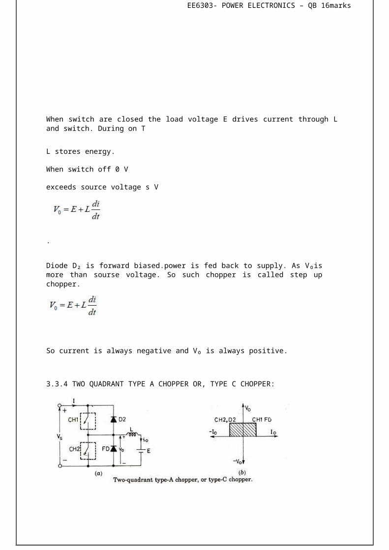
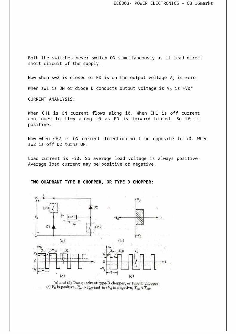
3.3.4 TWO QUADRANT TYPE A CHOPPER OR, TYPE C CHOPPER:
Both the switches never switch ON simultaneously as it lead direct short circuit of the supply.
Now when sw2 is closed or FD is on the output voltage V₀ is zero.
When sw1 is ON or diode D conducts output voltage is V₀ is +Vs‟
CURRENT ANANLYSIS:
When CH1 is ON current flows along i0. When CH1 is off current continues to flow along i0 as FD is forward biased. So i0 is positive.
Now when CH2 is ON current direction will be opposite to i0. When sw2 is off D2 turns ON.
Load current is –i0. So average load voltage is always positive. Average load current may be positive or negative.
TWO QUADRANT TYPE B CHOPPER, OR TYPE D CHOPPER:
EE6303- POWER ELECTRONICS – QB 16marks
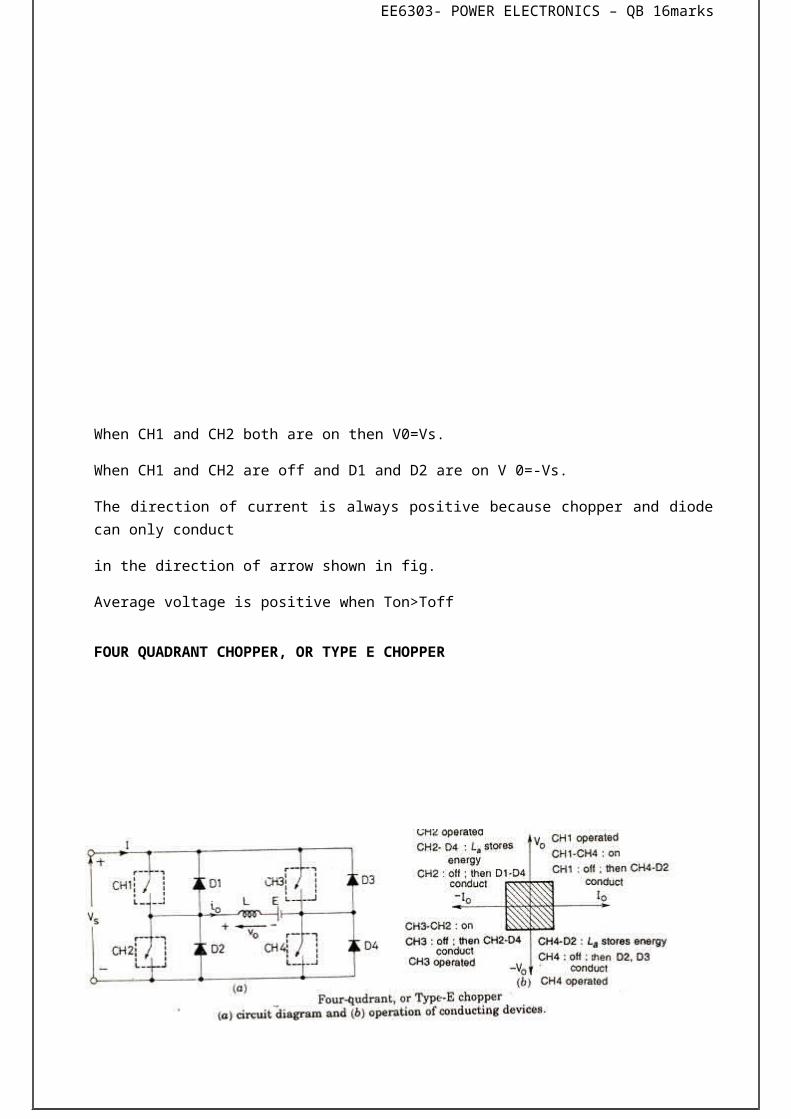
When CH1 and CH2 both are on then V0=Vs.
When CH1 and CH2 are off and D1 and D2 are on V 0=-Vs.
The direction of current is always positive because chopper and diode can only conduct
in the direction of arrow shown in fig.
Average voltage is positive when Ton>Toff
FOUR QUADRANT CHOPPER, OR TYPE E CHOPPER
EE6303- POWER ELECTRONICS – QB 16marks
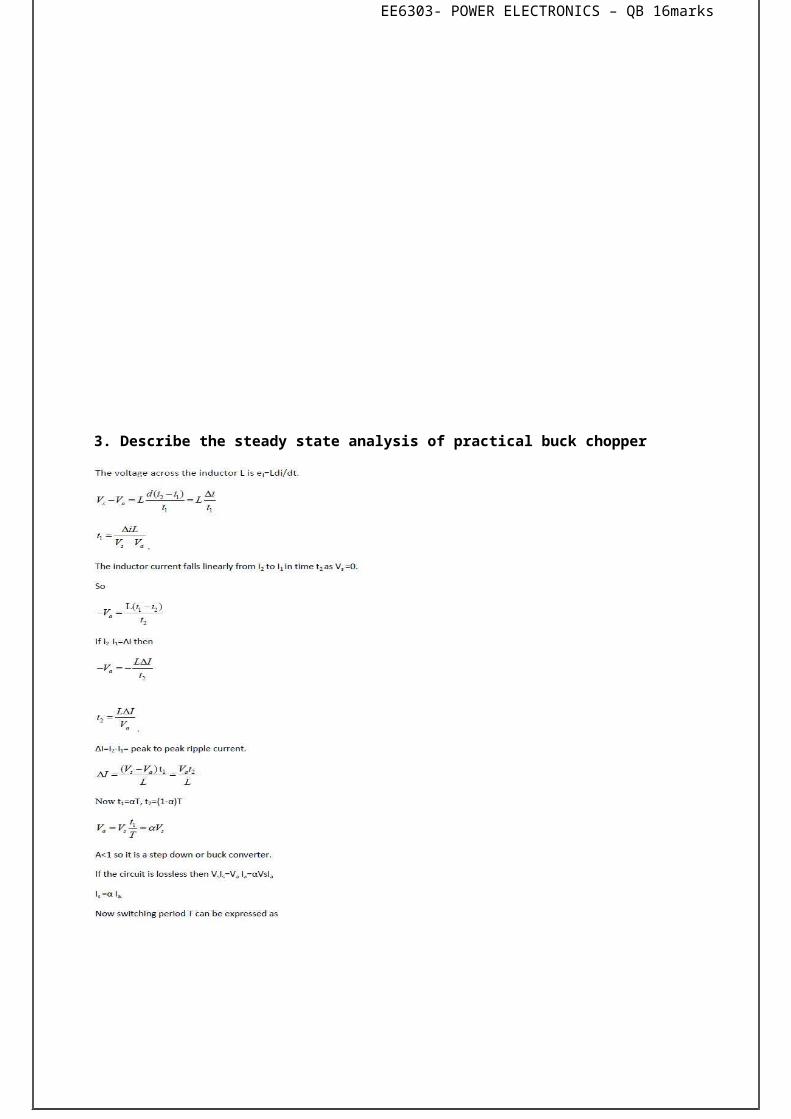
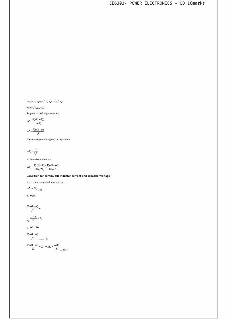
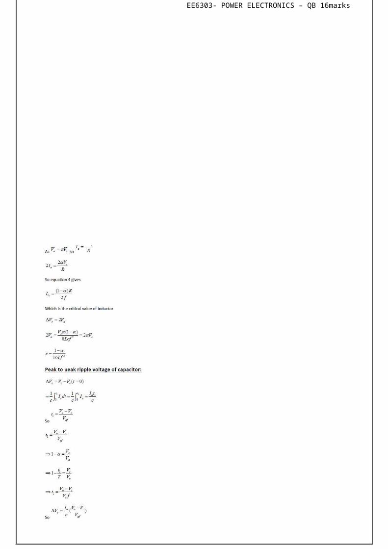
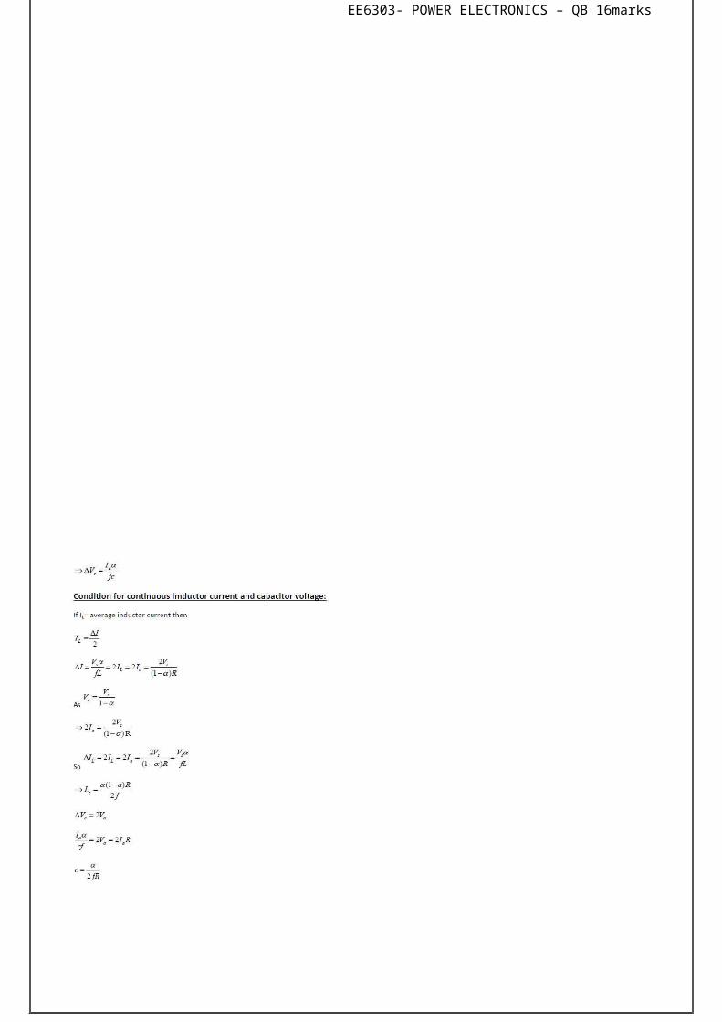
3. Describe the steady state analysis of practical buck chopper
EE6303- POWER ELECTRONICS – QB 16marks
EE6303- POWER ELECTRONICS – QB 16marks
EE6303- POWER ELECTRONICS – QB 16marks
EE6303- POWER ELECTRONICS – QB 16marks
1. Chopper:
It is a dc-dc converter which converts fixed dc voltage to variable dc voltage.
2. Duty Cycle:
The output voltage of the chopper can be controlled by varying (On and Off of the
semiconductor switch) the duty cycle of the chopper.
3. Time-Ratio control:
EE6303- POWER ELECTRONICS – QB 16marks
It is achieved by varying the Ton / T control.
4. Current Limit control:
In this control strategy chopper is switched On and Off so that the current in the load is
maintained between two limits. (Min. current when the chopper is On and Max. current when the
chopper is Off)
5. Step-up Chopper:
When the output voltage is greater than the input (E0>Edc), it corresponds to step-up
operation.
6. Breaking:
It is the process of stopping the machine which is under motion.
7. Commutation:
It is the process of turning-off of a power semiconductor device.
8. Forced commutation:
In this process, current through a power semiconductor device is forced to become zero to
turn-off.
9. Voltage commutation:
In this process, a charged capacitor momentarily reverse biases the conducting device and it turns
off.
10. Current commutation:
In this process, a current pulse is forced in the reverse direction through the conducting device. Now
the net current (forward and reverse current direction devices) becomes zero and the device is
turned off.
EE6303- POWER ELECTRONICS – QB 16marks
c. Load commutation:In this process, the load current flowing through the device either becomes
zero or is transferred to another device from the conducting device.
13. Harmonic Factor:
It is defined as the ratio of the total harmonic content to the fundamental component.
14. Ac regulators:
It converts fixed ac supply voltage and frequency to variable ac voltage without change in supply
frequency.
15. Cyclo-converters:
It converts fixed ac supply voltage and frequency to variable ac load frequency without change in
supply voltage.
UNIT IV
INVERTERS
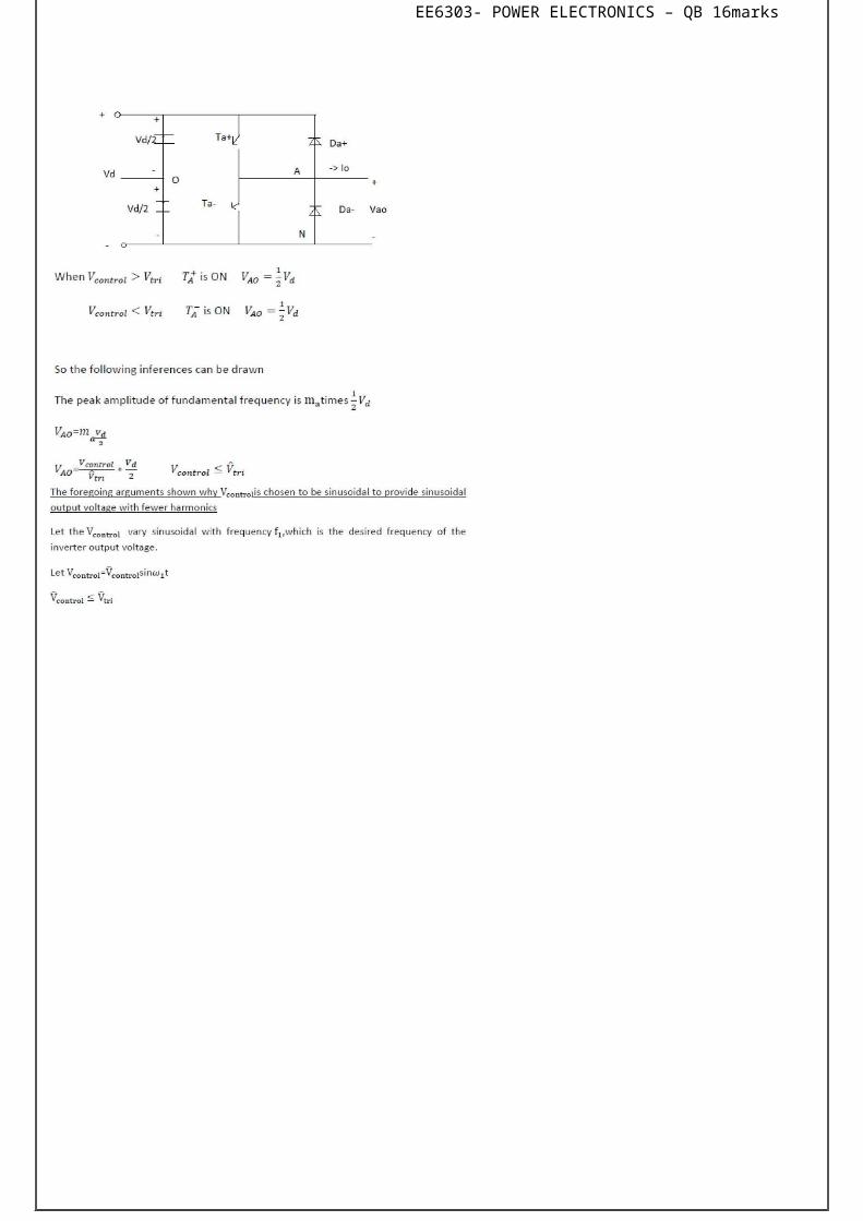
1. derive the expression for Single phase voltage source inverters
EE6303- POWER ELECTRONICS – QB 16marks
EE6303- POWER ELECTRONICS – QB 16marks
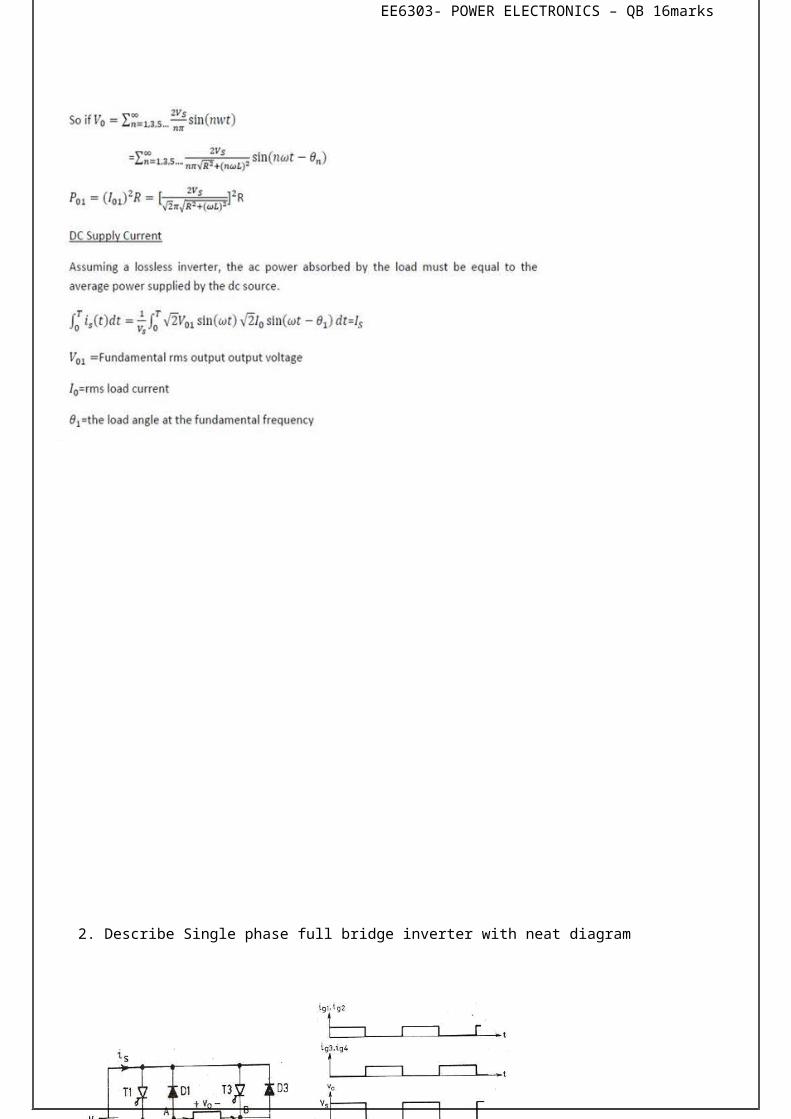
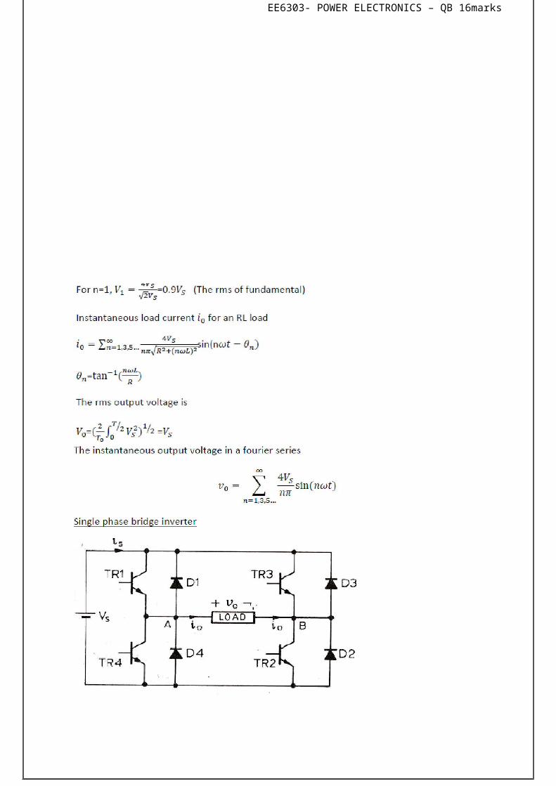
2. Describe Single phase full bridge inverter with neat diagram
EE6303- POWER ELECTRONICS – QB 16marks
EE6303- POWER ELECTRONICS – QB 16marks
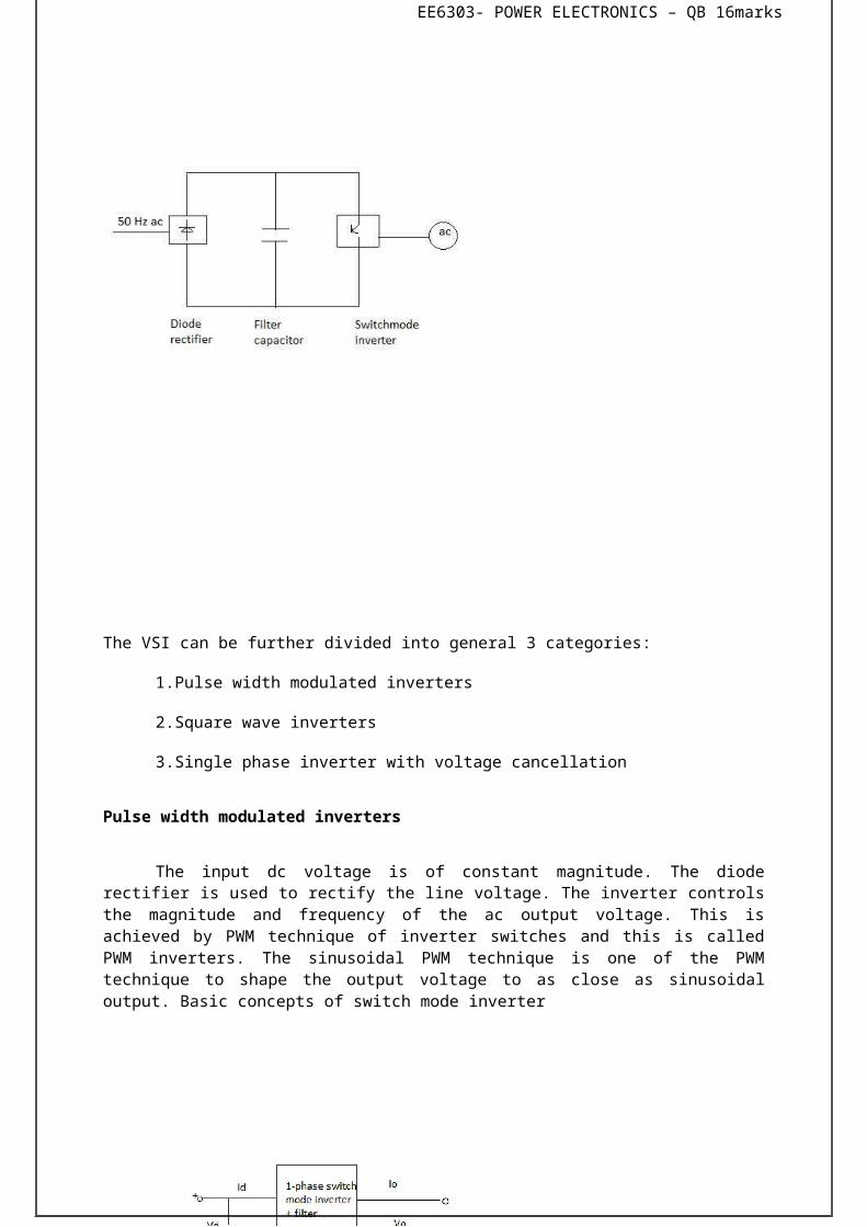
3. Explain the operation of VSI
Pulse width model
EE6303- POWER ELECTRONICS – QB 16marks
The VSI can be further divided into general 3 categories:
1.Pulse width modulated inverters
2.Square wave inverters
3.Single phase inverter with voltage cancellation
Pulse width modulated inverters
The input dc voltage is of constant magnitude. The diode rectifier is used to rectify the line voltage. The inverter controls the magnitude and frequency of the ac output voltage. This is achieved by PWM technique of inverter switches and this is called PWM inverters. The sinusoidal PWM technique is one of the PWM technique to shape the output voltage to as close as sinusoidal output. Basic concepts of switch mode inverter
EE6303- POWER ELECTRONICS – QB 16marks
.
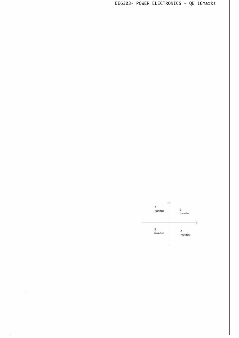
During interval 1 0and 0 both are positive
During interval 3 0 and 0 both are negative
Therefore during 1 and 3 the instantaneous power flow is from dc side to corresponding to inverter mode of operation.
In contrast during interval 2 and 4 0 and 0 are of opposite sign i.e. power flows from ac side to dc side corresponding to rectifier mode of operation.

EE6303- POWER ELECTRONICS – QB 16marks
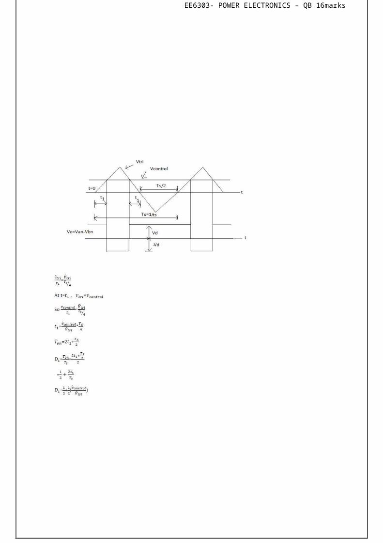
Pulse width modulated switching scheme
We require the inverter output to be sinusoidal with magnitude and frequency controllable. In order to produce sinusoidal output voltage at desired frequency a sinusoidal control signal at desired frequency is compared with a triangular waveform as show. The frequency of the triangular waveform established the inverter switching frequency. The triangular waveform is called carrier waveform. The triangular waveform establishes switching frequency , which establishes with which the inverter switches are applied.
The control signal has frequency and is used to modulate the switch duty ratio. 1 is the desired fundamental frequency of the output voltage.
The amplitude modulation ratio is defined as
is the peak amplitude of control signal.
peak amplitude of triangular signal.
The frequency modulation ratio

EE6303- POWER ELECTRONICS – QB 16marks
EE6303- POWER ELECTRONICS – QB 16marks
EE6303- POWER ELECTRONICS – QB 16marks
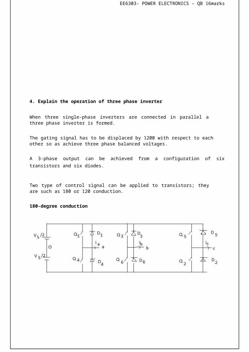
4. Explain the operation of three phase inverter
When three single-phase inverters are connected in parallel a three phase inverter is formed.
EE6303- POWER ELECTRONICS – QB 16marks
The gating signal has to be displaced by 1200 with respect to each other so as achieve three phase balanced voltages.
A 3-phase output can be achieved from a configuration of six transistors and six diodes.
Two type of control signal can be applied to transistors; they are such as 180 or 120 conduction.
180-degree conduction
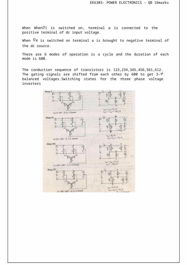
When When 1 is switched on, terminal a is connected to the positive terminal of dc input voltage.
When 4 is switched on terminal a is brought to negative terminal of the dc source.
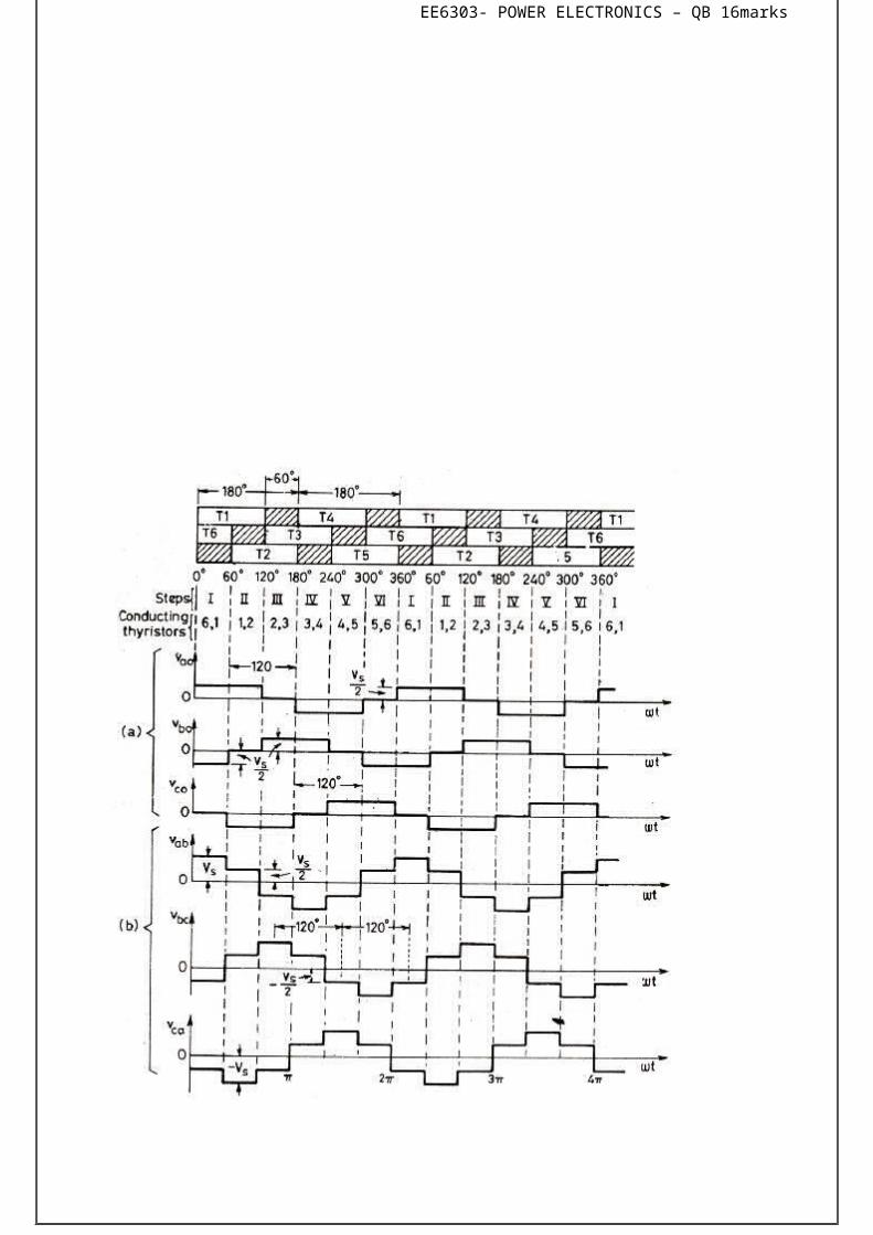
There are 6 modes of operation is a cycle and the duration of each mode is 600.
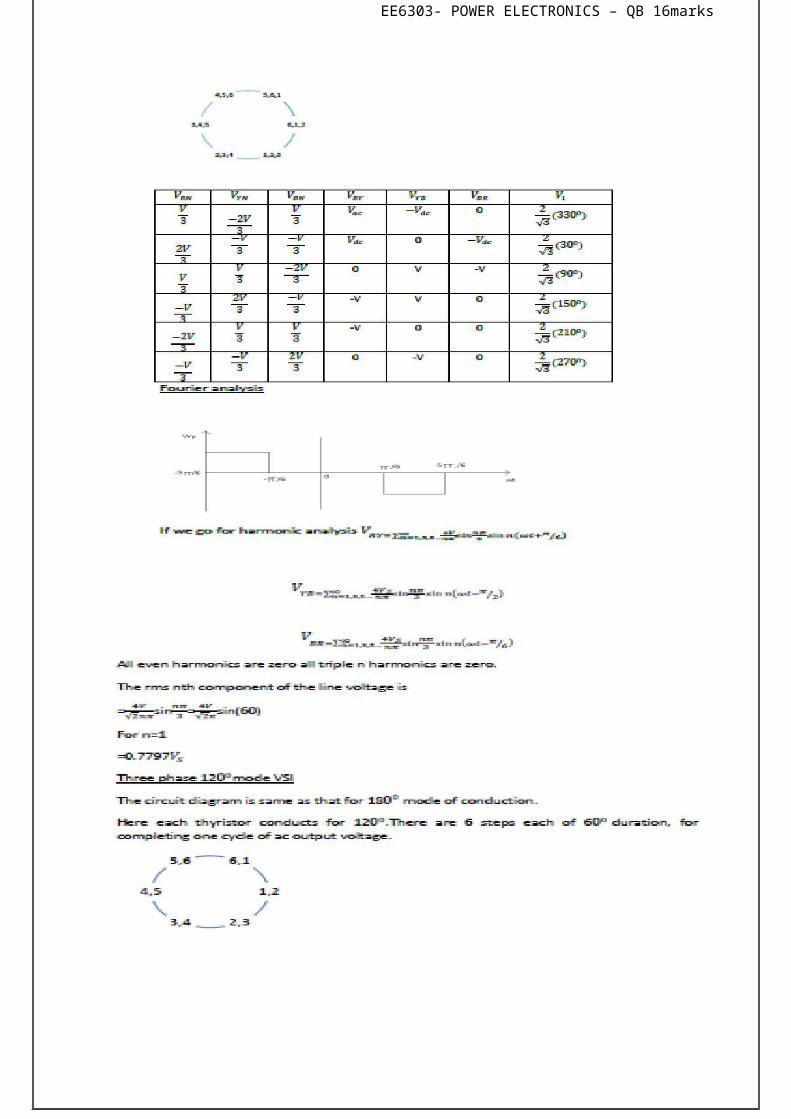
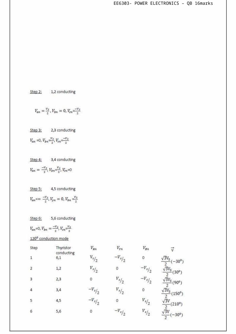
The conduction sequence of transistors is 123,234,345,456,561,612. The gating signals are shifted from each other by 600 to get 3- balanced voltages.Switching states for the three phase voltage inverters
EE6303- POWER ELECTRONICS – QB 16marks
EE6303- POWER ELECTRONICS – QB 16marks

EE6303- POWER ELECTRONICS – QB 16marks
EE6303- POWER ELECTRONICS – QB 16marks
EE6303- POWER ELECTRONICS – QB 16marks

EE6303- POWER ELECTRONICS – QB 16marks
EE6303- POWER ELECTRONICS – QB 16marks
EE6303- POWER ELECTRONICS – QB 16marks

EE6303- POWER ELECTRONICS – QB 16marks
1. Inverters:
Inverters are those which convert fixed dc voltage to variable ac output voltage and frequency.
2. Harmonics:
Harmonics are generated in the power electronic circuit due to the frequent turn-on and turn-off of the semiconductor devices. Due to this disturbances in the circuit, it causes fluctuations in the supply voltage, torque pulsations, low power factor, , increase of losses, less efficiency, etc.
3. PWM Technique:
In this technique, a fixed dc voltage is applied to the inverter as a input and a controlled ac output voltage is obtained by adjusting the ON and OFF period of the inverter devices.
4. Single-PWM:
In this scheme, there is only one pulse per half cycle and the width of the pulse is varied to control the inverter output voltage.
EE6303- POWER ELECTRONICS – QB 16marks
5. Multiple-PWM:
In this scheme, there are several pulses in each half cycle and the width of the pulse is varied to control the inverter output voltage. This method permits reduction in harmonic content up to low output voltage.
6. Comparator:
OP-amp acts as a comparator, which compares the carrier triangular signal and a dc reference signal.
7. Pulse Generator:
It generates trigger pulses/firing pulses; in order to turn-on the switching/power semiconductor devices.
8. Voltage source inverter:
In VSI the input dc voltage remains constant at low input impedance irrespective of ac voltage delivered to load.
9. Utility Factor:
It is the ratio of power delivered by the three-phase inverter when the load is 3- balanced to the total power rating of all switching devices of the bridges.
10. Current source inverter:
In CSI the input dc current from the dc source is maintained at an effectively constant level at high input impedance irrespective of load.

EE6303- POWER ELECTRONICS – QB 16marks

EE6303- POWER ELECTRONICS – QB 16marks
UNIT V
AC TO AC CONVERTERS
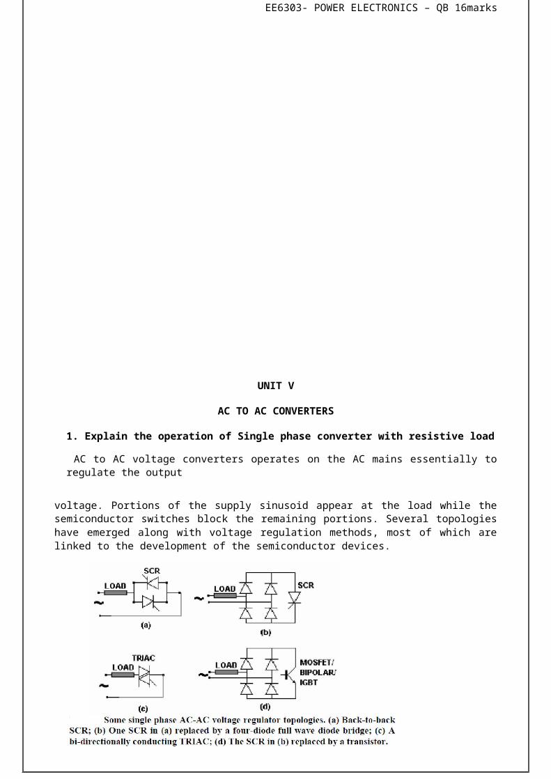
1. Explain the operation of Single phase converter with resistive load
AC to AC voltage converters operates on the AC mains essentially to regulate the output
voltage. Portions of the supply sinusoid appear at the load while the semiconductor switches block the remaining portions. Several topologies have emerged along with voltage regulation methods, most of which are linked to the development of the semiconductor devices.
They are called Phase Angle Controlled (PAC) AC-AC converters or AC-AC choppers. The TRIAC based converter may be considered as the basic topology. Being bi-directionally conducting devices, they act on both polarities of the applied voltage.

EE6303- POWER ELECTRONICS – QB 16marks
However, their ratings being poor, they tend to turn-on in the opposite direction just subsequent to their turn-off with an inductive load. The 'Alternistor' was developed with improved features but was not popular. The TRIAC is common only at the low power ranges. The (a) and (b) options are improvements on (c) mostly regarding current handling and turn-off-able current rating.
A transistorised AC-AC regulator is a PWM regulator similar to the DC-DC converters. It also requires a freewheeling path across the inductive load, which has also got to be bi-directional. Consequently, only controlled freewheeling devices can be used.
Operation with resistive loads
The device(s) is triggered at a phase-angle 'α' in each cycle. The current follows the voltage wave shape in each half and extinguishes itself at the zero crossings of the supply voltage. In the two-SCR topology, one SCR is positively biased in each half of the supply voltage. There is no scope for conduction overlap of the devices. A single pulse is sufficient to trigger the controlled devices with a resistive load. In the diode-SCR topology, two diodes are forward biased in each half. The SCR always receives a DC voltage and does not distinguish the polarity of the supply. It is thus always forward biased. The bi-directional TRIAC is also forward biased for both polarities of the supply voltage.
EE6303- POWER ELECTRONICS – QB 16marks

EE6303- POWER ELECTRONICS – QB 16marks
As is evident from the current waveforms, the PAC introduces significant harmonics both into the load and the supply. This is one of the main reasons why such controllers are today not acceptable. The ideal waveform as shown in Fig 26.2 is half wave symmetric. However it is to be achieved by the trigger circuits. The controller in Fig. 26.4 ensures this for the TRIAC based circuit. While the TRIAC has a differing characteristic for the two polarities of biasing with the 32V DIAC - a two terminal device- triggering is effected when the capacitor voltage reaches 32 V. This ensures elimination of DC and even components in the output voltage.
For the SCR based controllers, identical comparators for the two halves of the AC supply, which generates pulses for the two SCRs ensures DC and even harmonic free operation.
o
The PAC operates with a resistive load for all values of α ranging from 0 The fundamental current, if
can be represented as
EE6303- POWER ELECTRONICS – QB 16marks
In machine drives it is only the fundamental component, which is useful. However, in resistance heating type of application all harmonics are of no consequence. The corrupted supply current nevertheless is undesirable. Power Factor
The power factor of a nonlinear deserves a special discussion. Fig. 26.2 shows the supply voltage and the non-sinusoidal load current. The fundamental load/supply current lags the supply voltage by the φ1, 'Fundamental Power Factor' angle. Cosφ1 is also called
the 'Displacement Factor'. However this does not account for the total reactive power drawn by the system. This power factor is inspite of the actual load being resistive! The reactive power is drawn also y the trigger-angle dependent harmonics. Now
EE6303- POWER ELECTRONICS – QB 16marks
The portion within square brackets in Eq. 26.5 is identical to the first part of the expression within brackets in Eq. 26.1, which is called the Fourier coefficient 'B1
'.
The rms load voltage can also be similarly obtained by integrating between α and π and the result can be combined
2. Explain the operation of Single phase converter with Inductive load
With inductive loads the operation of the PAC is illustrated in Fig 26.5. The current builds up from zero in each cycle. It quenches not at the zero crossing of the applied voltage as with the resistive load but after that instant. The supply voltage thus continues to be impressed on the load till the load current returns to zero. A single-pulse trigger for the TRIAC 26.1 (c) or the anti-parallel SCR (b) has no effect on the devices if it (or the anti-parallel device) is already in conduction in the reverse direction. The devices would fail to conduct when they are intended to, as they do not have the supply voltage forward biasing them when the trigger pulse arrives. A single pulse trigger will work till the trigger
EE6303- POWER ELECTRONICS – QB 16marks
angle α > φ, where φ is the power factor angle of the inductive load. A train of pulses is required here. The output voltage is controllable only between triggering angles
o
φ and 180 .
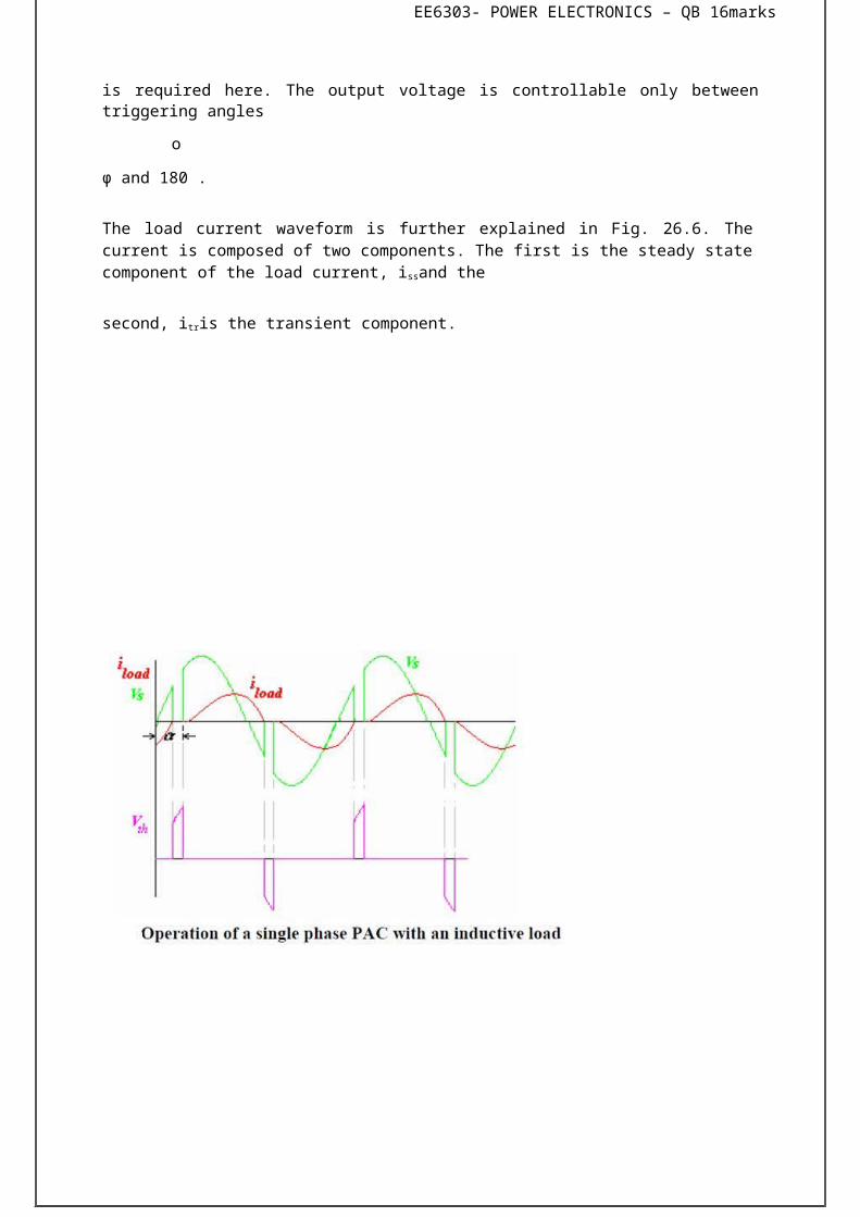
The load current waveform is further explained in Fig. 26.6. The current is composed of two components. The first is the steady state component of the load current, issand the
second, itris the transient component.
EE6303- POWER ELECTRONICS – QB 16marks
With an inductance in the load the distinguishing feature of the load current is that it must always start from zero. However, if the switch could have permanently kept the load connected to the supply the current would have become a sinusoidal one phase shifted from the voltage by the phase angle of the load, φ. This current restricted to the half periods of conduction is called the 'steady-state component' of load current iss. The
'transient component' of load current itr, again in each half cycle, must add up to zero with this i ssto start from zero. This condition sets the initial value of the transient component to that of the steady state at the instant that the SCR/TRIAC is triggered. Fig.
26.6 illustrates these relations.
When a device is in conduction, the load current is governed by the equation
The instant when the load current extinguishes is called the extinction angle β. It can be inferred that there would be no transients in the load current if the devices are triggered at the power factor angle of the load. The load current I that case is perfectly sinusoidal. Three-phase AC Regulators
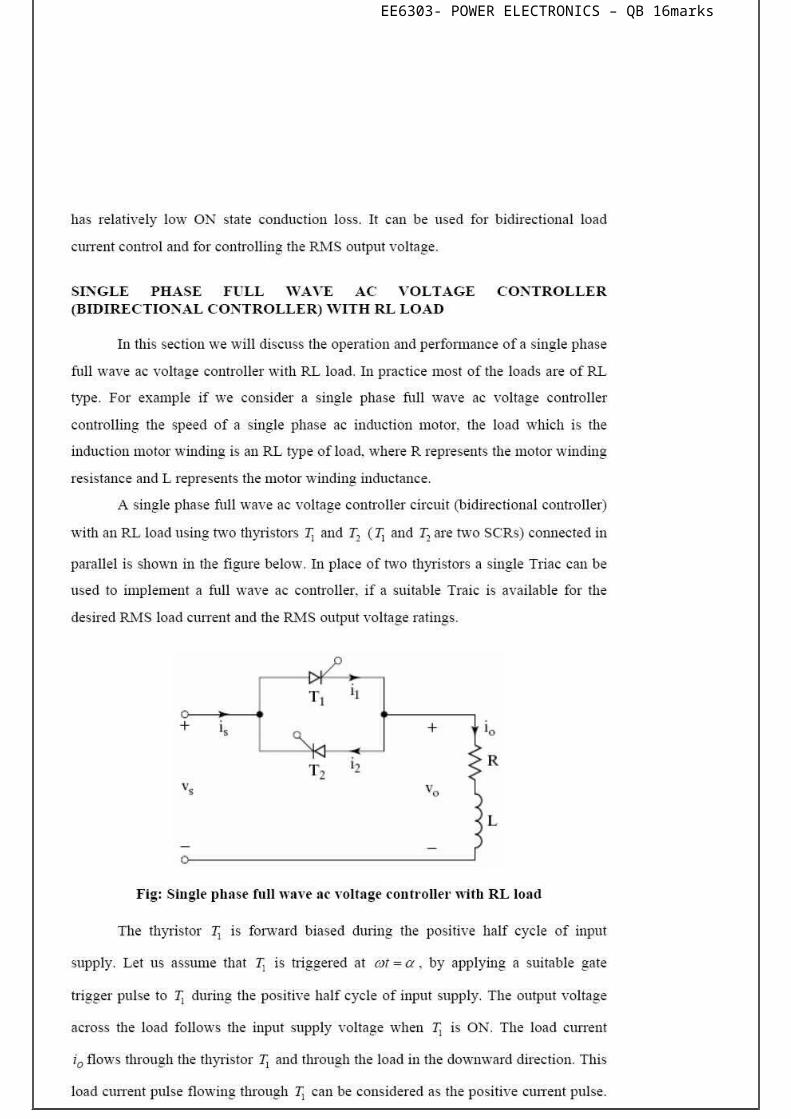
There are many types of circuits used for the three-phase ac regulators (ac to ac voltage converters), unlike single-phase ones. The three-phase loads (balanced) are connected in star or delta. Two thyristors connected back to back, or a triac, is used for each phase in mo most of the circuits as described. Two circuits are first taken up, both with balanced resistive (R) load
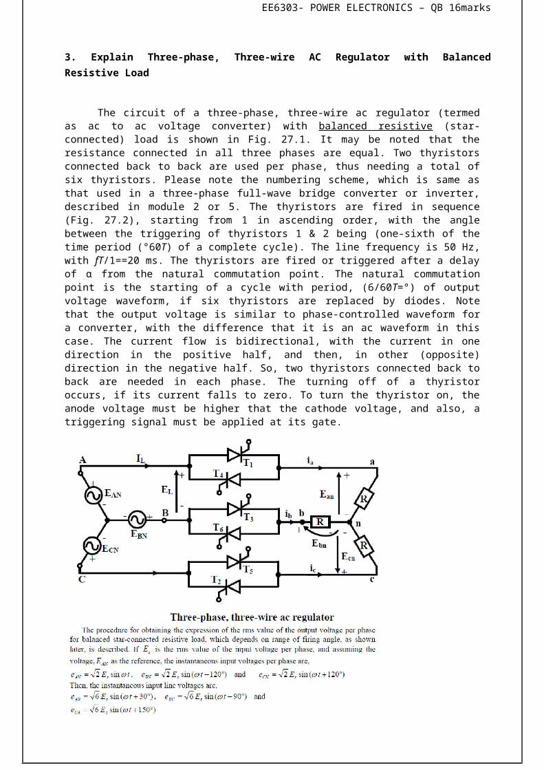
3. Explain Three-phase, Three-wire AC Regulator with Balanced Resistive Load
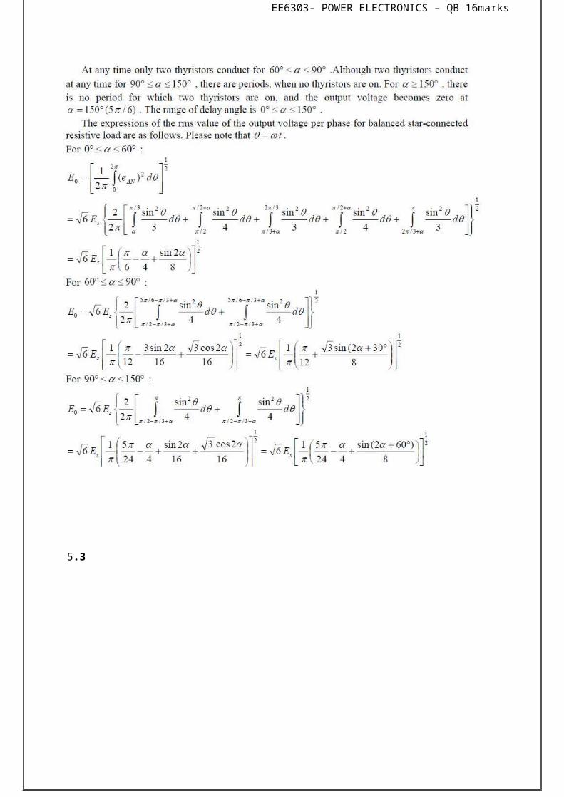
The circuit of a three-phase, three-wire ac regulator (termed as ac to ac voltage converter) with balanced resistive (star-connected) load is shown in Fig. 27.1. It may be noted that the resistance connected in all three phases are equal. Two thyristors connected back to back are used per phase, thus needing a total of six thyristors. Please note the numbering scheme, which is same as that used in a three-phase full-wave bridge converter or inverter, described in module 2 or 5. The thyristors are fired in sequence (Fig. 27.2), starting from 1 in ascending order, with the angle between the triggering of thyristors 1 & 2 being (one-sixth of the time period (°60T) of a complete cycle). The line frequency is 50 Hz, with fT/1==20 ms. The thyristors are fired or triggered after a delay of α from the natural commutation point. The natural commutation point is the starting of a cycle with period, (6/60T=°) of output voltage waveform, if six thyristors are replaced by diodes. Note that the output voltage is similar to phase-controlled waveform for a converter, with the difference that it is an ac
EE6303- POWER ELECTRONICS – QB 16marks
waveform in this case. The current flow is bidirectional, with the current in one direction in the positive half, and then, in other (opposite) direction in the negative half. So, two thyristors connected back to back are needed in each phase. The turning off of a thyristor occurs, if its current falls to zero. To turn the thyristor on, the anode voltage must be higher that the cathode voltage, and also, a triggering signal must be applied at its gate.
EE6303- POWER ELECTRONICS – QB 16marks
EE6303- POWER ELECTRONICS – QB 16marks
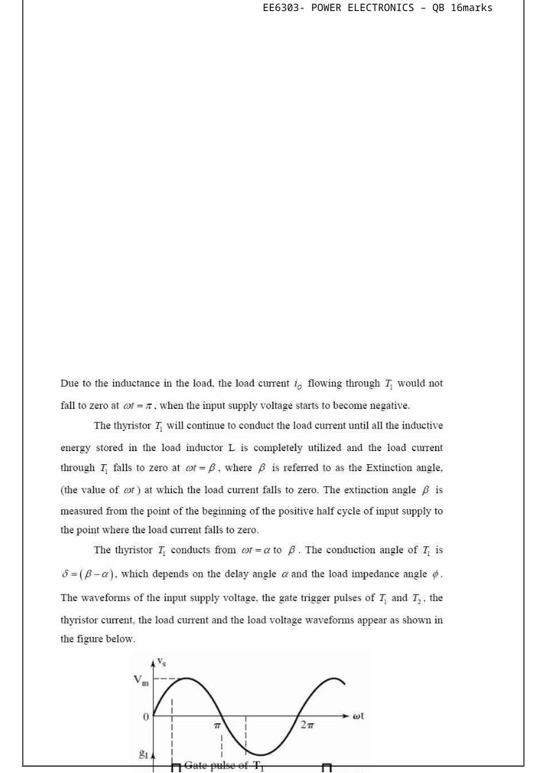
The waveforms of the input voltages, the conduction angles of thyristors and the output voltage of one phase, for firing delay angles (α) of (a) and (b) are shown in Fig. 27.2. For °60°120)6/(600πα°≤≤°, immediately before triggering of thyristor 1, two thyristors (5 & 6) conduct. Once thyristor 1 is triggered, three thyristors (1, 5 & 6) conduct. As stated earlier, a thyristor turns off, when the current through it goes to zero. The conditions alternate between two and three conducting thyristors.

EE6303- POWER ELECTRONICS – QB 16marks
EE6303- POWER ELECTRONICS – QB 16marks
5.3
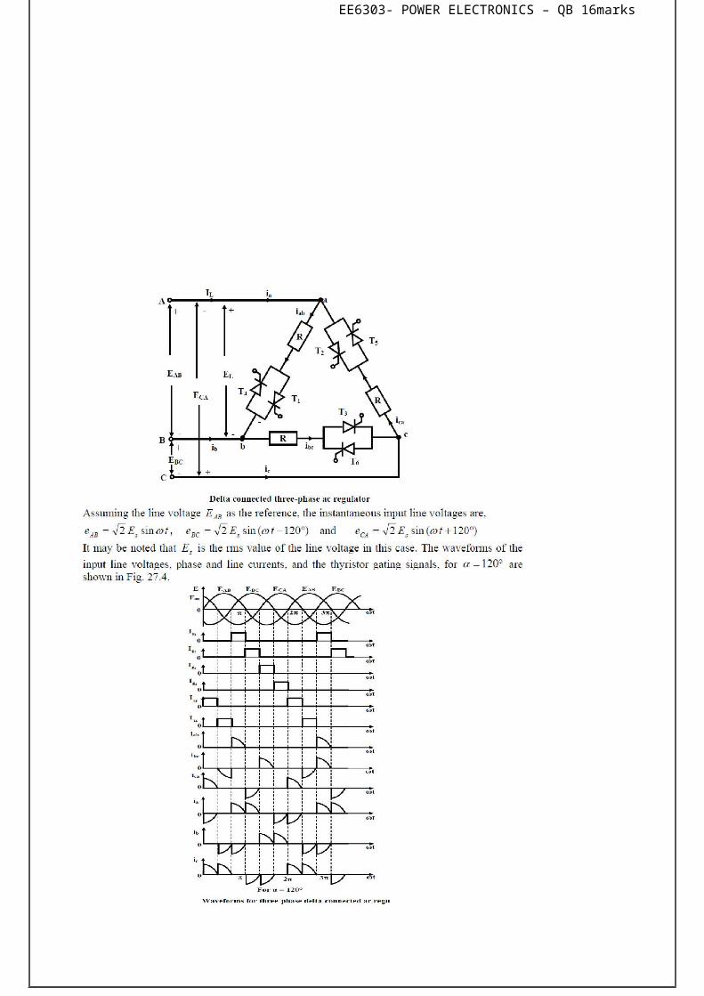
4. Explain the Three-phase Delta-connected AC Regulator with Balanced Resistive Load
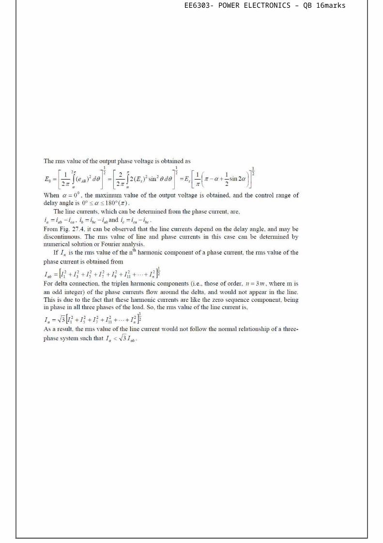
The circuit of a three-phase, delta-connected ac regulator (termed as ac to ac voltage converter) with balanced resistive load is shown in Fig. 27.3. It may be noted that the resistance connected in all three phases are equal. Two thyristors connected back to back are used per phase, thus needing a total of six thyristors. As stated earlier, the numbering scheme may be noted. It may be observed that one phase of the balanced circuit is similar to that used for single-phase ac regulator described in the previous lesson (26) of the module. Since the phase current in a balanced three-phase system is only (3/1 ) of the line current, the current rating of the thyristors would be lower than that if the thyristors are placed in the line.
EE6303- POWER ELECTRONICS – QB 16marks

EE6303- POWER ELECTRONICS – QB 16marks
EE6303- POWER ELECTRONICS – QB 16marks
EE6303- POWER ELECTRONICS – QB 16marks
5. Briefly explain AC voltage control techniques.
There are two different types of thyristor control used in practice to control the ac power flow
•On-Off control
•Phase control
These are the two ac output voltage control techniques.
In On-Off control technique Thyristors are used as switches to connect the load circuit to the ac supply (source) for a few cycles of the input ac supply and then to disconnect it for few input cycles. The Thyristors thus act as a high speed contactor (or high speed ac switch).
PHASE CONTROL
In phase control the Thyristors are used as switches to connect the load circuit to the input ac supply, for a part of every input cycle. That is the ac supply voltage is chopped using Thyristors during a part of each input cycle. The thyristor switch is turned on for a part of every half cycle, so that input supply voltage appears across the load and then turned off during the remaining part of input half cycle to disconnect the ac supply from the load.
By controlling the phase angle or the trigger angle „α‟ (delay angle), the output RMS voltage across the load can be controlled.
Phase control Thyristors which are relatively inexpensive, converter gradeThyristors which are slower than fast switching inverter grade Thyristors are normallyused.Forapplicationsupto 400Hz, if Triacs are available to meet the voltage andcurrent ratings of a particular application, Triacs are more commonly used.Due to ac line commutation or natural commutation, there is no need of extracommutation circuitry or components and the circuits for ac voltage controllers arevery simple.
EE6303- POWER ELECTRONICS – QB 16marks
Due to the nature of the output waveforms, the analysis, derivations ofexpressions for performance parameters are not simple, especially for the phasecontrolled ac voltage controllers with RL load. But however most of the practicalloads are of the RL type and hence RL load should be considered in the analysis anddesign of ac voltage controller circuits.
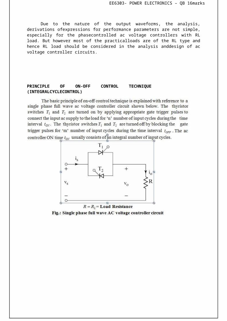
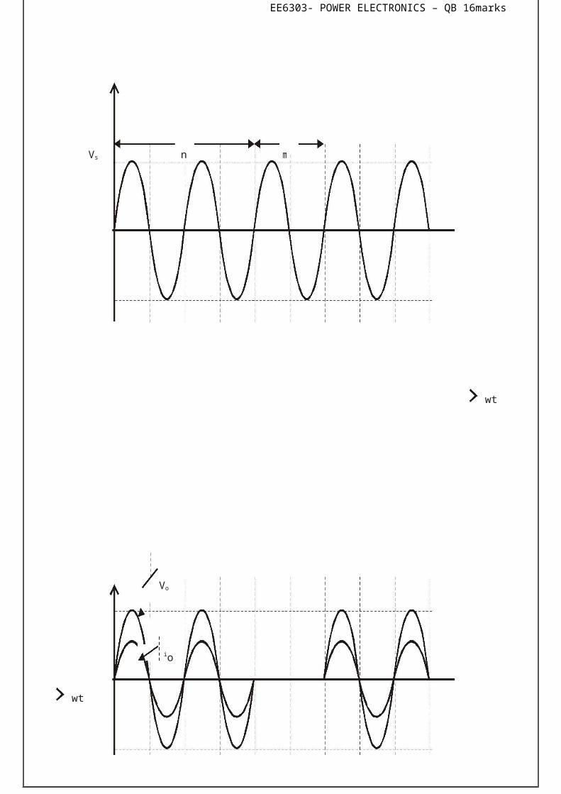
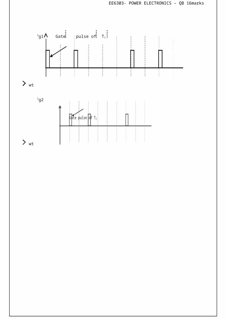
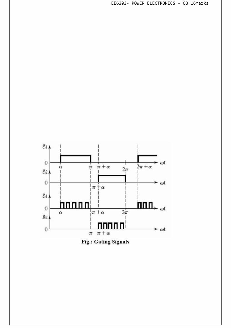
PRINCIPLE OF ON-OFF CONTROL TECHNIQUE (INTEGRALCYCLECONTROL)

EE6303- POWER ELECTRONICS – QB 16marks

EE6303- POWER ELECTRONICS – QB 16marks
Vs n m
wt
Vo
io
wt
EE6303- POWER ELECTRONICS – QB 16marks
ig1 Gate pulse of T1
wt
ig2
Gate pulse of T2
wt
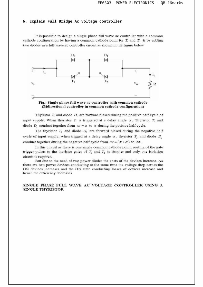
6. Explain Full Bridge Ac voltage controller.
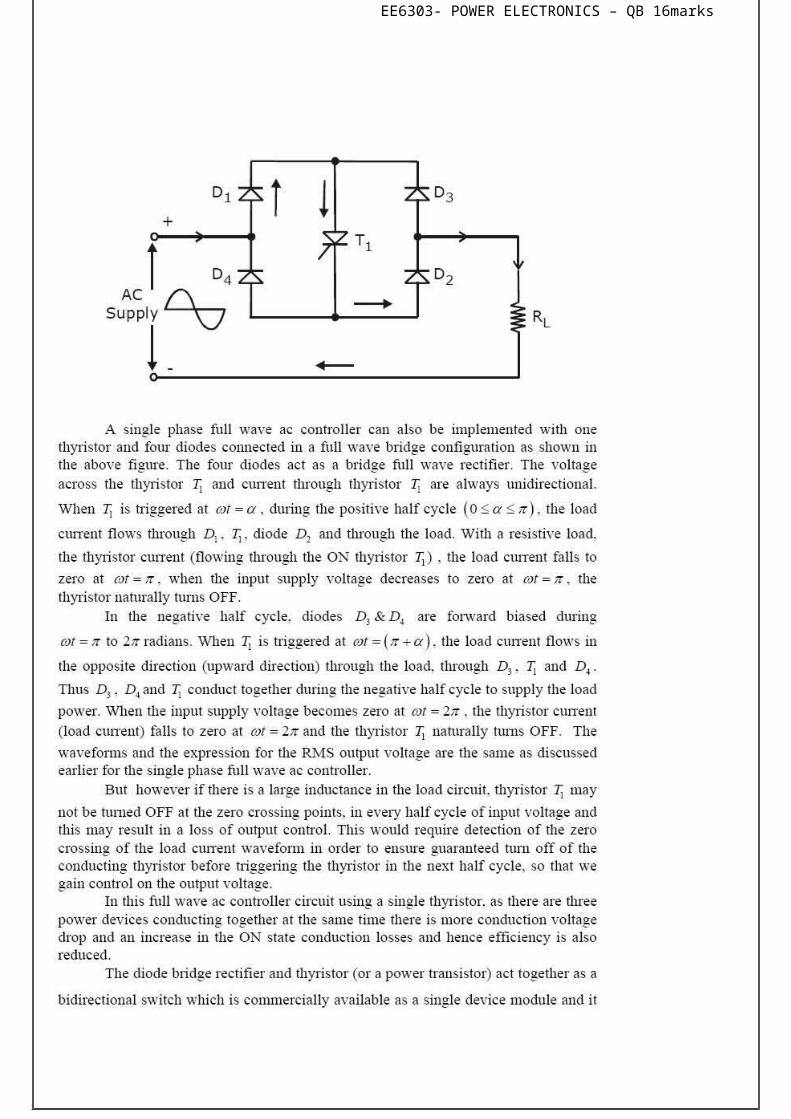
EE6303- POWER ELECTRONICS – QB 16marks
EE6303- POWER ELECTRONICS – QB 16marks
EE6303- POWER ELECTRONICS – QB 16marks

EE6303- POWER ELECTRONICS – QB 16marks
EE6303- POWER ELECTRONICS – QB 16marks
EE6303- POWER ELECTRONICS – QB 16marks
EE6303- POWER ELECTRONICS – QB 16marks

EE6303- POWER ELECTRONICS – QB 16marks
EE6303- POWER ELECTRONICS – QB 16marks
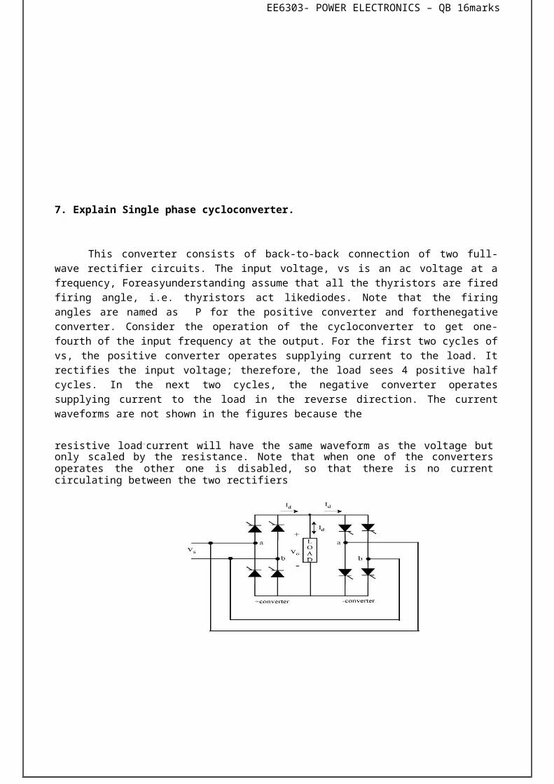
7. Explain Single phase cycloconverter.
This converter consists of back-to-back connection of two full-wave rectifier circuits. The input voltage, vs is an ac voltage at a frequency, Foreasyunderstanding assume that all the thyristors are fired firing angle, i.e. thyristors act likediodes. Note that the firing angles are named as P for the positive converter and forthenegative converter. Consider the operation of the cycloconverter to get one-fourth of the input frequency at the output. For the first two cycles of vs, the positive converter operates supplying current to the load. It rectifies the input voltage; therefore, the load sees 4 positive half cycles. In the next two cycles, the negative converter operates supplying current to the load in the reverse direction. The current waveforms are not shown in the figures because the
resistive load.current will have the same waveform as the voltage but only scaled by the resistance. Note that when one of the converters operates the other one is disabled, so that there is no current circulating between the two rectifiers
EE6303- POWER ELECTRONICS – QB 16marks
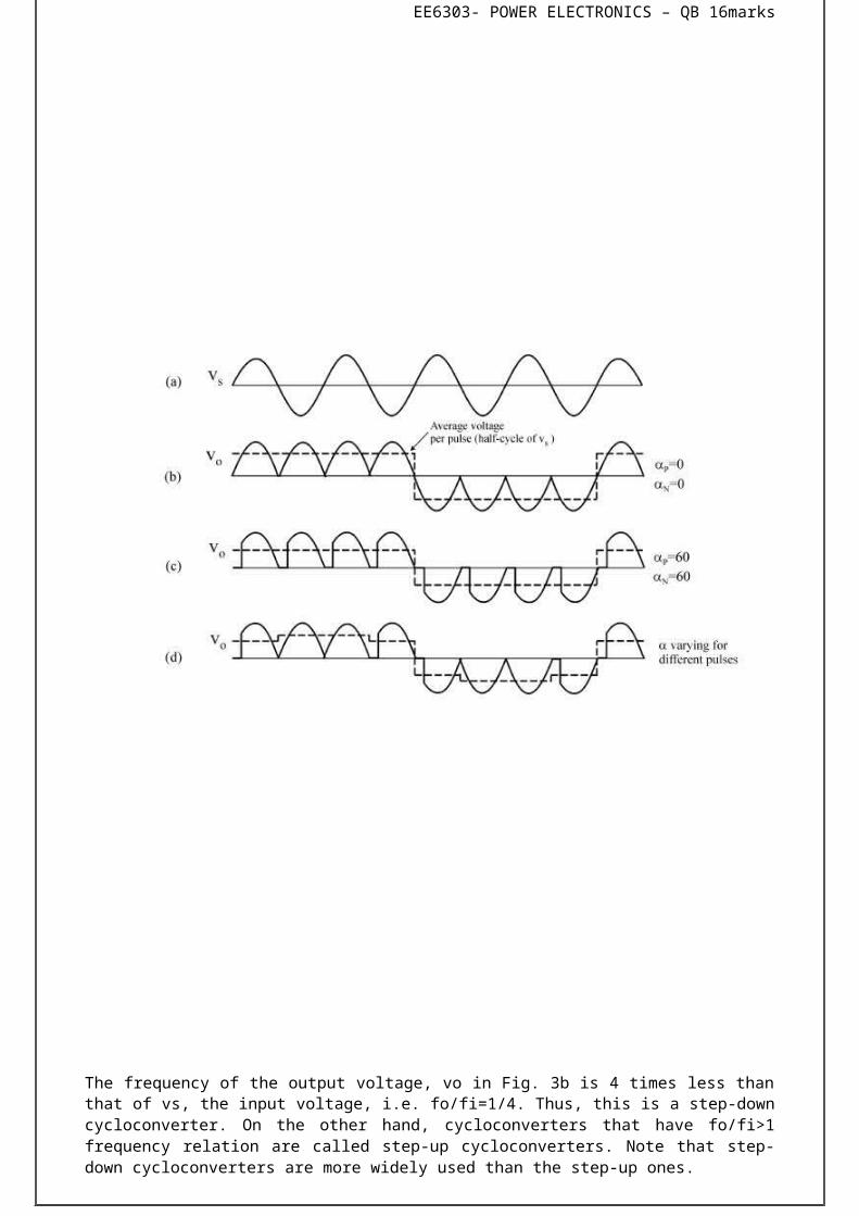
The frequency of the output voltage, vo in Fig. 3b is 4 times less than that of vs, the input voltage, i.e. fo/fi=1/4. Thus, this is a step-down cycloconverter. On the other hand, cycloconverters that have fo/fi>1 frequency relation are called step-up cycloconverters. Note that step-down cycloconverters are more widely used than the step-up ones.
The frequency of vo can be changed by varying the number of cycles the positive and the negative converters work. It can only change as integer multiples of fi in 1f-1f cycloconverters.
With the above operation, the 1f-1f cycloconverter can only supply a certain voltage at a certain firing angle a. The dc output of each rectifier is:
EE6303- POWER ELECTRONICS – QB 16marks
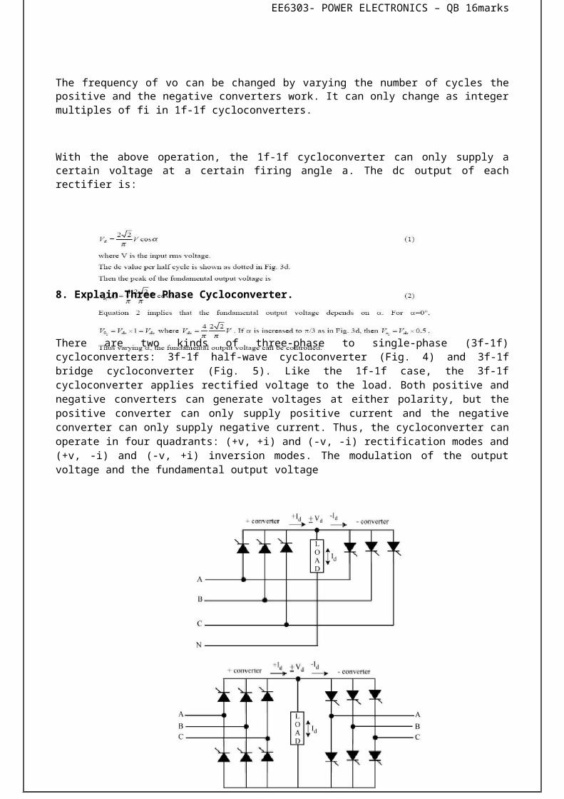
8. Explain Three Phase Cycloconverter.
There are two kinds of three-phase to single-phase (3f-1f) cycloconverters: 3f-1f half-wave cycloconverter (Fig. 4) and 3f-1f bridge cycloconverter (Fig. 5). Like the 1f-1f case, the 3f-1f cycloconverter applies rectified voltage to the load. Both positive and negative converters can generate voltages at either polarity, but the positive converter can only supply positive current and the negative converter can only supply negative current. Thus, the cycloconverter can operate in four quadrants: (+v, +i) and (-v, -i) rectification modes and (+v, -i) and (-v, +i) inversion modes. The modulation of the output voltage and the fundamental output voltage

EE6303- POWER ELECTRONICS – QB 16marks
The polarity of the current determines if the positive or negative converter should be supplying power to the load. Conventionally, the firing angle for the positive converter is named aP, and that of the negative converter is named aN. When the polarity of the current changes, the converter previously supplying the current is disabled and the other one is enabled. The load always requires the fundamental voltage to be continuous. Therefore, during the current polarity reversal, the average
EE6303- POWER ELECTRONICS – QB 16marks
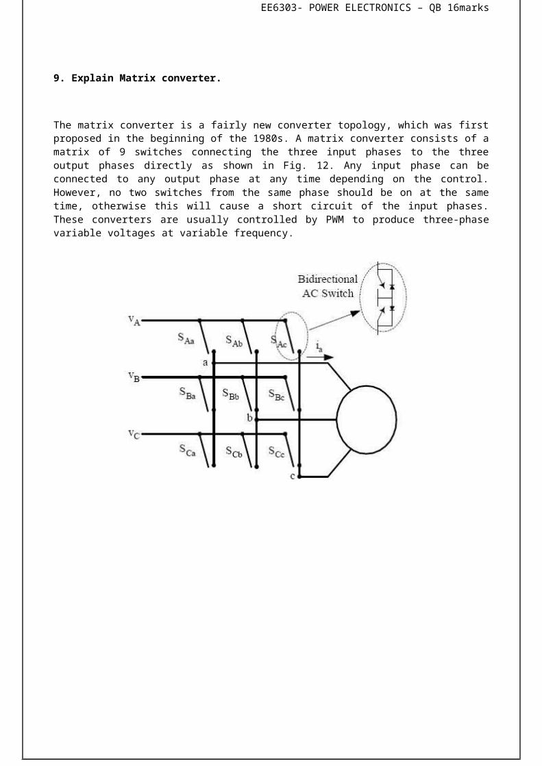
9. Explain Matrix converter.
The matrix converter is a fairly new converter topology, which was first proposed in the beginning of the 1980s. A matrix converter consists of a matrix of 9 switches connecting the three input phases to the three output phases directly as shown in Fig. 12. Any input phase can be connected to any output phase at any time depending on the control. However, no two switches from the same phase should be on at the same time, otherwise this will cause a short circuit of the input phases. These converters are usually controlled by PWM to produce three-phase variable voltages at variable frequency.

EE6303- POWER ELECTRONICS – QB 16marks
This direct frequency changer is not commonly used because of the high device count, i.e. 18 switches compared to 12 of a dc link rectifier-inverter system. However, the devices used are smaller because of their shorter ON time compared to the latter.
Single-Phase to Three-Phase (1f-3f) Cycloconverters:
Recently, with the decrease in the size and the price of power electronics switches, single-phase to three-phase cycloconverters (1f-3f) started drawing more research interest. Usually, an H-bridge inverter produces a high frequency single-phase voltage waveform, which is fed to the cycloconverter either through a high frequency transformer or not. If a transformer is used, it isolates
the inverter from the cycloconverter. In addition to this, additional taps from the transformer can be used to power other converters producing a high frequency ac link. The single-phase high frequency ac (hfac) voltage can be either sinusoidal or trapezoidal. There might be zero voltage intervals for control purposes
EE6303- POWER ELECTRONICS – QB 16marks
or zero voltage commutation. Fig. 13 shows the circuit diagram of a typical hfac link converter. These converters are not commercially available yet. They are in the research state.
Among several kinds, only two of them will be addressed here:
Integral Pulse Modulated (1f-3f) Cycloconverters
The input to these cycloconverters is single-phase high frequency sinusoidal or square waveforms with or without zero voltage gaps. Every half-cycle of the input signal, the control for each phase decides if it needs a positive pulse or a negative pulse using integral pulse modulation. For integral pulse modulation, the command signal and the output phase voltage are integrated and the latter result is subtracted from the former. For a positive difference, a negative pulse is required, and vice versa for the negative difference. For the positive (negative) input half-cycle, if a positive pulse is required, the upper (lower) switch is turned on; otherwise, the lower (upper) switch is turned on.
Therefore, the three-phase output voltage consists of positive and negative half-cycle pulses of the input voltage. Note that this converter can only work at output frequencies which are multiples of the input frequency.
Fig. 13 High frequency ac link converter (1f hf inverter + (1f-3f) Cycloconverter)

EE6303- POWER ELECTRONICS – QB 16marks
Phase-Controlled (1f-3f) Cycloconverter
This cycloconverter converts the single-phase high frequency sinusoidal or square wave voltage into three-phase voltages using the previously explained phase control principles. The voltage command is compared to a sawtooth waveform to find the firing instant of the switches. Depending on the polarity of the current and the input voltage, the next switch to be turned on is determined. Compared to the previous one, this converter has more complex control but it can work at any frequency.
Question Bank
UNIT – I
POWER SEMI-CONDUCTOR DEVICES
1. What is meant by thyristor converter system?2. What is the difference between power diode and signal level diode?3. Define reverse recovery time in diodes.4. Define safe operating area.5. What are the different methods to turn on the thyristor?6. Define latching and holding current.7. List the advantages of GTO over SCR?8. Distinguish between SCR, TRIAC and GTO.9. What is snubber circuit?10. What is the drawback of SCR over BJT?11. What is DIAC and how it differs from SCR?12. Draw the symbol of TRIAC, GTO, MOSFET and IGBT.13. Compare MOSFET and BJT.14. Why IGBT is very popular now a day?15. IGBT and MOSFET is voltage controlled device why?16. Why MOSFETs are preferred for high frequency applications?
17. List the important features of IGBT.18. Define circuit turn-off time19. Why circuit turn-off time should be greater than the thyristor turn-off time?
20. What is the basis for selection of power semiconductor device for a particular application?
PART- B
EE6303- POWER ELECTRONICS – QB 16marks
1. i. Enumerate the importance of series and parallel operation of an SCR with relevant sketches.
a. .Discuss the various methods of turning on of SCR.
iii. Explain the two transistor analogy of SCR. iv.Explain about the dV/dt and di/dt protection in an SCR.
2. Draw the symbol and structure of TRIAC. Explain all the four triggering modes of operation with neat sketch.
3. i. Explain the construction, operation and switching characteristics of SCR.ii. Explain the construction, operation and switching characteristics of BJT.iii. Explain about the secondary breakdown in BJT.
4. i. Explain the construction, operation and switching characteristics of MOSFET.ii. Explain the construction, operation and switching characteristics of IGBT.
EE6303- POWER ELECTRONICS – QB 16marks
UNIT – II
PHASE CONTROLLED CONVERTER
PART A
1.What is meant by phase controlled rectifier?2.Mention some of the applications of controlled rectifiers.3.Classify controlled rectifiers.4.Define delay or firing angle.5.Define extinction angle.
6. Differentiate between line and forced commutation.
14. What is commutation angle or overlap angle?15. What is the function of freewheeling diode in controlled rectifiers?16. List the advantages of freewheeling diodes.
10. What is the inversion mode of rectifiers?11. Why the power factor of semi converter is greater than full converter?12. What is meant by input power factor in controlled rectifier?13. What are the advantages of six pulse converter?14. Distinguish between two and four quadrant converters.15. What are ac voltage controllers and give few applications?16. List the merits and demerits of ac voltage controllers.17. List the strategies available for control of ac voltage controllers.18. Distinguish between ON-OFF and integral cycle control.19. What are the two types of ac voltage controllers? Which one of these is preferred, why?20. What is meant by full wave or bidirectional ac voltage controller?
PART- B
1.Explain the principle of operation and derive the expressions for average output voltage and RMS output voltage of the following,
a. Single-phase half controlled rectifier feeding R loadb. Single-phase full controlled rectifier feeding RL load
c. Single-phase two quadrant and two pulse converter operating on rectification and Inversion modes.
f. Explain the operation of three-phase half and full converter rectifier feeding RL load. With the aid of neat waveforms and also derive the expression for average output voltage.
g. Explain the effect of source impedance on the performance of converters.
h. Explain the operation of Single-phase ac voltage controller having only thyristors feeding resistive load by on-off and phase control. Derive the expression for rms value of output voltage in both cases.
EE6303- POWER ELECTRONICS – QB 16marks
i. Explain the principle of operation of Single-phase ac voltage controllers with necessary circuit and waveforms.
EE6303- POWER ELECTRONICS – QB 16marks
UNIT III
DC TO DC CONVERTER
PART- A
1. What is chopper and list its applications?2. What are the advantages of dc chopper?3. Define duty cycle.4. What are the two types of control strategies used in choppers?5. What is meant by frequency modulation control in dc chopper?6. What is meant by pulse width modulation control in dc chopper?7. What are the types of TRC?8. What is current limit control?9. Differentiate between step-up and step-down chopper.10. What is continuous current operation?11. Draw the circuit diagram of Buck-Boost chopper.12. Why voltage commutated chopper is extensively used?13. What are four quadrant choppers?14. What is meant by Cycloconverters? List its types.15. What are the applications of Cycloconverters?
PART- B
1. Explain the operation of step-up and step down choppers. Also derive the expressions for the output voltage.
2. With the aid of power circuit explain the Class A to Class E copper configurations.3. Derive an expression for duty ratio of buck boost converter.
18. With relevant sketches explain the operation of a voltage, current and load commutated chopper.
19. Explain the operation of the following,a. Single phase to single phase bridge type Cycloconvertersb. Three phase to single phase Cycloconverters.
UNIT IV
INVERTERS
PART- A
1. What are inverters, list its applications.2. How inverters are classified based on the commutation circuitry?3. How the output frequency is varied in an inverter?4. Why diodes should be connected in anti parallel with the thyristors in inverter circuits?5. Why thyristors are not preferred for inverters?6. What is inverter gain?
EE6303- POWER ELECTRONICS – QB 16marks
7. Mention the methods available for the output voltage control of inverters.8. What is meant by PWM control?9. List the different types of PWM techniques.10. What are the advantages of PWM techniques in inverters?11. Compare VSI and CSI.12. What are the applications of CSI?13. What are the drawbacks of the presence of harmonics in inverters?
14. What are the methods of reduction of harmonic content?
PART- B
1. Explain the operation of single-phase half bridge inverter with aid of relevant waveforms and derive the instantaneous output voltage.
2. Explain the operation of single-phase full bridge inverter with aid of relevant waveforms and derive the instantaneous output voltage.
3. i. Explain the principle of operation of current source inverter.ii. Explain the principle of operation of auto sequential 1 current sourceinverter?
4. i. Explain three-phase 1800 degree conduction mode of inverter.ii. Explain three-phase 1200 degree conduction mode of inverter.
5. What is the need for controlling the output voltage of inverters and state the different methods of voltage control of single phase inverters. Describe the single phase sinusoidal PWM control with relevant waveforms.
6. Write short notes on, Harmonic reduction.
UNIT V AC TO AC CONVERTERS 1.What is the difference betweenON-OFF control and phase control?
2. What is the advantage of ON-OFF control?3. What is the disadvantage ofON-OFF control?4. What is the duty cycle in ON-OFF control method?5. What is meant by unidirectional or half-wave ac voltage controller?6. What are the disadvantages of unidirectional or half-wave ac voltage controller?7. What is meant by bidirectional or half-wave ac voltage controller?
8. What is the control range of firing angle in ac voltage controller with RL load?9. What type of gating signal is used in single phase ac voltage controller with RL load?10. What are the disadvantages of continuous gating signal?11. What is meant by high frequency carrier gating?12. What is meant by sequence control ofac voltage regulators?21. What are the advantages ofsequence control of ac voltage regulators?22. What is meant by cyclo-converter?23. What are the two types of cyclo-converters?24. What is meant by step-up cyclo-converters?25. What is meantby step-down cyclo-converters?26. What are the applications of cyclo-converter?27. What is meant by positive converter groupin a cyclo converter?28. What is meant by negative converter group in a cyclo converter?
PART-B
EE6303- POWER ELECTRONICS – QB 16marks
1. Draw the circuit diagramof 1_capacitor commutated currentsource inverter and explain its operation with equivalent circuits for different modes and necessary waveforms.
2. Explain the operation of multistage controlof AC voltagecontrollers withneat diagram.
3. Explain the operation of 1_ ACvoltage controller with RL load.4. Explain the operation of sequence control of AC voltagecontroller..5 Explain the operation of 1_ sinusoidal AC voltagecontroller..
EE6303- POWER ELECTRONICS – QB 16marks
EE6303- POWER ELECTRONICS – QB 16marks
EE6303- POWER ELECTRONICS – QB 16marks