virtex-6 fpga gth transceivers - xilinx...virtex-6 fpga gth transceivers user guide ug371 (v2.2)...
TRANSCRIPT

Virtex-6 FPGA GTH Transceivers
User Guide
UG371 (v2.2) June 29, 2011

Virtex-6 FPGA GTH Transceivers User Guide www.xilinx.com UG371 (v2.2) June 29, 2011
The information disclosed to you hereunder (the “Materials”) is provided solely for the selection and use of Xilinx products. To the maximum extent permitted by applicable law: (1) Materials are made available "AS IS" and with all faults, Xilinx hereby DISCLAIMS ALL WARRANTIES AND CONDITIONS, EXPRESS, IMPLIED, OR STATUTORY, INCLUDING BUT NOT LIMITED TO WARRANTIES OF MERCHANTABILITY, NON-INFRINGEMENT, OR FITNESS FOR ANY PARTICULAR PURPOSE; and (2) Xilinx shall not be liable (whether in contract or tort, including negligence, or under any other theory of liability) for any loss or damage of any kind or nature related to, arising under, or in connection with, the Materials (including your use of the Materials), including for any direct, indirect, special, incidental, or consequential loss or damage (including loss of data, profits, goodwill, or any type of loss or damage suffered as a result of any action brought by a third party) even if such damage or loss was reasonably foreseeable or Xilinx had been advised of the possibility of the same.
Xilinx assumes no obligation to correct any errors contained in the Materials or to notify you of updates to the Materials or to product specifications. You may not reproduce, modify, distribute, or publicly display the Materials without prior written consent. Certain products are subject to the terms and conditions of the Limited Warranties which can be viewed at http://www.xilinx.com/warranty.htm; IP cores may be subject to warranty and support terms contained in a license issued to you by Xilinx. Xilinx products are not designed or intended to be fail-safe or for use in any application requiring fail-safe performance; you assume sole risk and liability for use of Xilinx products in Critical Applications: http://www.xilinx.com/warranty.htm#critapps.
© Copyright 2009–2011 Xilinx, Inc. Xilinx, the Xilinx logo, Artix, ISE, Kintex, Spartan, Virtex, Zynq, and other designated brands included herein are trademarks of Xilinx in the United States and other countries. All other trademarks are the property of their respective owners.
UG371 (v2.2) June 29, 2011 www.xilinx.com Virtex-6 FPGA GTH Transceivers User Guide
Revision HistoryThe following table shows the revision history for this document.
Date Version Revision
09/16/09 1.0 Initial Xilinx release.
02/16/10 2.0 Changed the clock domain for the RXPOWERDOWNx[1:0] ports in Table 1-2, page 15, Table 2-11, page 57, and Table 2-13, page 71.Chapter 1: Updated OTU-3 values in Table 1-1. In Table 1-2, renamed DO port to DRPDO and relocated ports I, IB, and O to new Table 1-3.Chapter 2: In the GTHRESET description in Table 2-7 and Table 2-11, indicated that GTHINIT must be pulsed only after GTHRESET is deasserted. In Table 2-11 and Table 2-13, changed RXPOWERDOWN and TXPOWERDOWN descriptions for the x4 link case. Added Reference Clock Input Structure, page 43. Removed reference to LVDS clocks as being able to drive the reference clock pins, page 44. Added sentence about MMCM and BUFR to TSTREFCLKOUT port description in Table 2-4. Added PLL, page 48. Revised Figure 2-16, Figure 2-17, and Figure 2-18. In Table 2-12, changed the meaning of bit code 110 for bits [13:11] and [10:8] of the PCS_MODE_LANE attribute to Reserved; changed the 8B/10B reset value for the PCS_RESET_LANE attribute; added reference to the Virtex-6 FPGA GTH Transceiver Wizard to attribute PCS_RESET_1_LANE, bits [15:2]. In Table 2-15, added the encoding to the PMA_LPBK_CTRL_LANE attribute description; changed the Reserved bits for [13:11] and [10:8] in the PCS_MODE_LANE attribute; added reference to the Virtex-6 FPGA GTH Transceiver Wizard to attribute PMA_LPBK_CTRL_LANE, bits [15:2]. In Table 2-16, changed the name of port DO[15:0] to DRPDO[15:0]. Added note about DISABLEDRP to Using the DRP Interface, page 78 and Using the Management Interface, page 80. Chapter 3: Added 32 and 64 bits to 8B/10B mode in Table 3-1. Added two rows to 8B/10B Mode for 32-bit and 64-bit fabric interface data width in Table 3-2. Revised manual adjustment mode settings for the BUFFER_CONFIG_LANE attribute in Table 3-4, and changed the meaning of bit code 110 for bits [13:11] and [10:8] of the PCS_MODE_LANE attribute to Reserved in Table 3-4, Table 3-6, Table 3-8, and Table 3-10. Added reference to the Virtex-6 FPGA GTH Transceiver Wizard to attribute PCS_RESET_1_LANE, bits [15:2] in Table 3-6. Changed the 8B/10B reset value for the PCS_RESET_LANE attribute in Table 3-6, Table 3-8, Table 3-10, and Table 3-12. Added reference to the Virtex-6 FPGA GTH Transceiver Wizard to attribute PCS_RESET_1_LANE, bits [15:2] in Table 3-10. Changed the PCS_RESET_LANE value in step 2 of Enabling 8B/10B Mode, page 93. In Table 3-12, and added reference to the Virtex-6 FPGA GTH Transceiver Wizard to attribute PRBS_CFG_LANE, bits [15:4] and PCS_RESET_1_LANE, bits [15:2]; changed the Reserved bits for [13:11] and [10:8] in the PCS_MODE_LANE attribute. In Table 3-13, added reference to the Virtex-6 FPGA GTH Transceiver Wizard to attribute PCS_MISC_CFG_0_LANE, bits [15:12] and [5:0]. Added TX Configurable Driver.Chapter 4: Added RX Analog Front End, RX Equalization, and RX CDR. Added reference to the Virtex-6 FPGA GTH Transceiver Wizard to attribute PCS_MISC_CFG_0_LANE, bits [15:12] and [5:0] in Table 4-9, and to attributes PCS_MISC_CFG_0_LANE, bits [15:12] and [5:0], PCS_RESET_1_LANE bits [15:2], and PRBS_CFG_LANE bits [15:4] in Table 4-11. In the Functional Description section of RX Pattern Checker, added paragraph about when the checker is forced into PRBS31 mode, and added two sentences at the end of the section. Added Table 4-10. Changed the 8B/10B reset value for the PCS_RESET_LANE attribute in Table 4-11, Table 4-14, Table 4-17, and Table 4-19. Deleted PRBS checker reference in Description of RXCODEERR in Table 4-13, Table 4-16, Table 4-18, and Table 4-22. In Table 4-14, Table 4-17, Table 4-19, and Table 4-23, changed transmitter to receiver in the description of RX_FABRIC_WIDTH, and changed the meaning of bit code 110 for bits [13:11] and [10:8] of the PCS_MODE_LANE attribute to Reserved. In Table 4-14, Table 4-17, and Table 4-19, added reference to the Virtex-6 FPGA GTH Transceiver Wizard to attribute PCS_RESET_1_LANE, bits [15:2]. Changed the PCS_RESET_LANE value in step 2 of Enabling 8B/10B Mode, page 140. Added 32 and 64 bits to 8B/10B mode in Table 4-20. Added two rows to 8B/10B Mode for 32-bit and 64-bit fabric interface data width in Table 4-21. Revised manual adjustment mode settings for the BUFFER_CONFIG_LANE attribute in Table 4-23. Added Chapter 5, Board Design Guidelines.
Virtex-6 FPGA GTH Transceivers User Guide www.xilinx.com UG371 (v2.2) June 29, 2011
10/04/10 2.1 Chapter 1: Updated the list of supported line rates for multiple industry standards on page 11. Updated the GTHE1_QUAD columns in Figure 1-1. Removed Table 1-1: PLL Settings for Protocol Standards. Added the RXDATATAP#, RXPCSCLKSMPL#, TXDATATAP#, and TXPCSCLKSMPL# ports to Table 1-2 and changed the GTHRESET clock domain.Chapter 2: Updated the definitions for the PLL_CFG1 attribute in Table 2-3. Added lane divider settings to Table 2-6 and revised the line rate range for lane divider 4. Updated the three dividers to generate different PCS clocks on page 50. In Table 2-7, revised the GTHRESET, RXRATE#, and SAMPLERATE#, and TXRATE descriptions. In Table 2-9, revised PLL_CFG0 and PLL_CFG1 descriptions. In Table 2-10, revised the OC-48, OTU1, OTU3, and OTU4 settings and added XLAUI CAUI, and note 2. In Table 2-11, revised the GTHRESET, RXRATE#, SAMPLERATE#, and TXRATE descriptions. In Table 2-12, added LANE_PWR_CTRL_LANE#, RX_CFG1_LANE#, RX_CFG0_LANE#, MISC_CFG, and TX_CLK_SEL1_LANE#. Replaced the 1 with a 20 in the areas that require asserting the GTHRESET for 20 DCLK clock cycles (page 66 and page 68). Updated discussion under Near-end PMA Loopback section. Updated Figure 2-18. Updated description for PMA_LPBK_CTRL_LANE# in Table 2-15. Added a caveat on asserting GTHRESET under the Using the DRP Interface and Using the Management Interface sections. Added section on Differences Between the DRP and Management Interfaces.Chapter 3: Updated [5:0] in Table 3-13. In Table 3-15, updated descriptions for TX_PREEMPH_LANE# and TX_CFG0_LANE#.Chapter 4: Updated receiver common mode comment in Table 4-1. In Table 4-7: Updated RX_CDR_CTRL1_LANE description. In Table 4-9, updated [5:0] description. Removed RX polarity in near-end PCS loopback mode restriction from Using RX Polarity Control discussion. In Table 4-11, updated PCS_MISC_CFG_0_LANE# [5:0] description. In Table 4-12, updated register names.Chapter 5: Added sections on Board Design Guidelines – Analog Power Supply Pins, Voltage Regulators with Remote Voltage Sensing, Power Supply Distribution Network, MGTHAVCC Decoupling Capacitor Layout, Printed Circuit Board Design, and Signal BGA Breakout.Appendix B, DRP Address Map of GTH Transceivers: Added this appendix.
06/29/11 2.2 Updated Legal Disclaimer. Chapter 1: Added notes to Figure 1-1 through Figure 1-12.Chapter 2: Added Note in Functional Description for Figure 2-5 description. Added Table 2-8. In Table 2-10, inserted additional row for OTU3 and OTU4. Added DISABLE_DRP and MGMT interface signals to Table 2-11. Revised steps in GTH Quad Initialization in Response to Completion of Configuration, revised Figure 2-6, added Figure 2-7, revised Figure 2-8, and added Figure 2-9. Revised steps in GTH Quad Reset in Response to GTHRESET, revised Figure 2-10, added Figure 2-11, revised Figure 2-12, and added Figure 2-13. In Table 2-15, added LANE_AMON_SE attribute, revised description of PMA_LPBK_CTRL_LANE# and PCS_MODE_LANE#, added SLICE_CFG attribute. Added AC-JTAG section.Chapter 3, Transmitter: Added Note to Enabling 64B/66B Mode section.Chapter 4: Revised description of RX_CFG2_LANE# in Table 4-3. In Table 4-5, added RX_AEQ_MON0_LANE# and RX_AEQ_MON1_LANE# attributes, revised description of RX_AEQ_VAL0_LANE# and RX_AEQ_VAL1_LANE# attributes, added RX_AGC_CTRL_LANE# attributes, and added default to RX_CTLE_CTRL_LANE# attributes. Changed title of Setting the RX Equalization to Use Mode: Channel Loss up to 8 dB with No TX Emphasis. Revised AGC section and Table 4-6. Revised DFE and CTLE sections. Added Use Mode: General Operation section. Added Note to Enabling 64B/66B Mode section.Chapter 5: Added Power Supply Sequencing section.Appendix A, Low Latency Design of GTH Transceivers: Added this appendix.Appendix B, DRP Address Map of GTH Transceivers (previously Appendix A): In Table B-1, added RX_AEQ_MON0_LANE# and RX_AEQ_MON1_LANE# attributes.
Date Version Revision

Virtex-6 FPGA GTH Transceivers User Guide www.xilinx.com 5UG371 (v2.2) June 29, 2011
Revision History . . . . . . . . . . . . . . . . . . . . . . . . . . . . . . . . . . . . . . . . . . . . . . . . . . . . . . . . . . . . . 3Guide Contents . . . . . . . . . . . . . . . . . . . . . . . . . . . . . . . . . . . . . . . . . . . . . . . . . . . . . . . . . . . . . . 9Additional Documentation . . . . . . . . . . . . . . . . . . . . . . . . . . . . . . . . . . . . . . . . . . . . . . . . . . . 9Additional Resources . . . . . . . . . . . . . . . . . . . . . . . . . . . . . . . . . . . . . . . . . . . . . . . . . . . . . . . 10
Chapter 1: Transceiver and Tool OverviewOverview . . . . . . . . . . . . . . . . . . . . . . . . . . . . . . . . . . . . . . . . . . . . . . . . . . . . . . . . . . . . . . . . . . . 11Port and Attribute Summary . . . . . . . . . . . . . . . . . . . . . . . . . . . . . . . . . . . . . . . . . . . . . . . . 14Virtex-6 FPGA GTH Transceiver Wizard. . . . . . . . . . . . . . . . . . . . . . . . . . . . . . . . . . . . . 30Simulation . . . . . . . . . . . . . . . . . . . . . . . . . . . . . . . . . . . . . . . . . . . . . . . . . . . . . . . . . . . . . . . . . . 31
Functional Description . . . . . . . . . . . . . . . . . . . . . . . . . . . . . . . . . . . . . . . . . . . . . . . . . . . . 31Ports and Attributes. . . . . . . . . . . . . . . . . . . . . . . . . . . . . . . . . . . . . . . . . . . . . . . . . . . . . . . 31
Implementation . . . . . . . . . . . . . . . . . . . . . . . . . . . . . . . . . . . . . . . . . . . . . . . . . . . . . . . . . . . . . 31Functional Description . . . . . . . . . . . . . . . . . . . . . . . . . . . . . . . . . . . . . . . . . . . . . . . . . . . . 31FF1155 Package Diagrams . . . . . . . . . . . . . . . . . . . . . . . . . . . . . . . . . . . . . . . . . . . . . . . . . 33FF1923 and FF1924 Package Diagrams . . . . . . . . . . . . . . . . . . . . . . . . . . . . . . . . . . . . . . . 36
Chapter 2: Shared Transceiver FeaturesReference Clock Input Structure . . . . . . . . . . . . . . . . . . . . . . . . . . . . . . . . . . . . . . . . . . . . . 43
Functional Description . . . . . . . . . . . . . . . . . . . . . . . . . . . . . . . . . . . . . . . . . . . . . . . . . . . . 43Ports and Attributes. . . . . . . . . . . . . . . . . . . . . . . . . . . . . . . . . . . . . . . . . . . . . . . . . . . . . . . 44Using the Reference Clock . . . . . . . . . . . . . . . . . . . . . . . . . . . . . . . . . . . . . . . . . . . . . . . . . 44
Reference Clock Distribution and Selection . . . . . . . . . . . . . . . . . . . . . . . . . . . . . . . . . 45Functional Description . . . . . . . . . . . . . . . . . . . . . . . . . . . . . . . . . . . . . . . . . . . . . . . . . . . . 45Ports and Attributes. . . . . . . . . . . . . . . . . . . . . . . . . . . . . . . . . . . . . . . . . . . . . . . . . . . . . . . 45Clocking from an External Source . . . . . . . . . . . . . . . . . . . . . . . . . . . . . . . . . . . . . . . . . . . 46Clocking from a Neighboring GTH Quad . . . . . . . . . . . . . . . . . . . . . . . . . . . . . . . . . . . . 46
PLL . . . . . . . . . . . . . . . . . . . . . . . . . . . . . . . . . . . . . . . . . . . . . . . . . . . . . . . . . . . . . . . . . . . . . . . . . 48Functional Description . . . . . . . . . . . . . . . . . . . . . . . . . . . . . . . . . . . . . . . . . . . . . . . . . . . . 48Ports and Attributes. . . . . . . . . . . . . . . . . . . . . . . . . . . . . . . . . . . . . . . . . . . . . . . . . . . . . . . 52PLL Settings for the Common Protocol . . . . . . . . . . . . . . . . . . . . . . . . . . . . . . . . . . . . . . 55
Reset and Initialization. . . . . . . . . . . . . . . . . . . . . . . . . . . . . . . . . . . . . . . . . . . . . . . . . . . . . . 56Functional Description . . . . . . . . . . . . . . . . . . . . . . . . . . . . . . . . . . . . . . . . . . . . . . . . . . . . 56Ports and Attributes. . . . . . . . . . . . . . . . . . . . . . . . . . . . . . . . . . . . . . . . . . . . . . . . . . . . . . . 57GTH Quad Initialization in Response to Completion of Configuration . . . . . . . . . . . 63GTH Quad Reset in Response to GTHRESET . . . . . . . . . . . . . . . . . . . . . . . . . . . . . . . . . 66Resetting the Transmit Datapath . . . . . . . . . . . . . . . . . . . . . . . . . . . . . . . . . . . . . . . . . . . . 70Resetting the Receive Datapath . . . . . . . . . . . . . . . . . . . . . . . . . . . . . . . . . . . . . . . . . . . . . 71
Power Down . . . . . . . . . . . . . . . . . . . . . . . . . . . . . . . . . . . . . . . . . . . . . . . . . . . . . . . . . . . . . . . . 71Functional Description . . . . . . . . . . . . . . . . . . . . . . . . . . . . . . . . . . . . . . . . . . . . . . . . . . . . 71Ports and Attributes. . . . . . . . . . . . . . . . . . . . . . . . . . . . . . . . . . . . . . . . . . . . . . . . . . . . . . . 71Using Power Down . . . . . . . . . . . . . . . . . . . . . . . . . . . . . . . . . . . . . . . . . . . . . . . . . . . . . . . 72
Loopback . . . . . . . . . . . . . . . . . . . . . . . . . . . . . . . . . . . . . . . . . . . . . . . . . . . . . . . . . . . . . . . . . . . 73Functional Description . . . . . . . . . . . . . . . . . . . . . . . . . . . . . . . . . . . . . . . . . . . . . . . . . . . . 73
Table of Contents

6 www.xilinx.com Virtex-6 FPGA GTH Transceivers User GuideUG371 (v2.2) June 29, 2011
Far-end Loopback . . . . . . . . . . . . . . . . . . . . . . . . . . . . . . . . . . . . . . . . . . . . . . . . . . . . . . 73Near-end PCS Loopback. . . . . . . . . . . . . . . . . . . . . . . . . . . . . . . . . . . . . . . . . . . . . . . . . 73Near-end PMA Loopback . . . . . . . . . . . . . . . . . . . . . . . . . . . . . . . . . . . . . . . . . . . . . . . . 74
Ports and Attributes. . . . . . . . . . . . . . . . . . . . . . . . . . . . . . . . . . . . . . . . . . . . . . . . . . . . . . . 75AC-JTAG . . . . . . . . . . . . . . . . . . . . . . . . . . . . . . . . . . . . . . . . . . . . . . . . . . . . . . . . . . . . . . . . . . . 77
Functional Description . . . . . . . . . . . . . . . . . . . . . . . . . . . . . . . . . . . . . . . . . . . . . . . . . . . . 77Dynamic Reconfiguration Port . . . . . . . . . . . . . . . . . . . . . . . . . . . . . . . . . . . . . . . . . . . . . . 78
Functional Description . . . . . . . . . . . . . . . . . . . . . . . . . . . . . . . . . . . . . . . . . . . . . . . . . . . . 78Ports and Attributes. . . . . . . . . . . . . . . . . . . . . . . . . . . . . . . . . . . . . . . . . . . . . . . . . . . . . . . 78Using the DRP Interface . . . . . . . . . . . . . . . . . . . . . . . . . . . . . . . . . . . . . . . . . . . . . . . . . . . 78
Management Interface . . . . . . . . . . . . . . . . . . . . . . . . . . . . . . . . . . . . . . . . . . . . . . . . . . . . . . 79Functional Description . . . . . . . . . . . . . . . . . . . . . . . . . . . . . . . . . . . . . . . . . . . . . . . . . . . . 79Ports and Attributes. . . . . . . . . . . . . . . . . . . . . . . . . . . . . . . . . . . . . . . . . . . . . . . . . . . . . . . 79Using the Management Interface . . . . . . . . . . . . . . . . . . . . . . . . . . . . . . . . . . . . . . . . . . . . 80
Differences Between the DRP and Management Interfaces. . . . . . . . . . . . . . . . . . . 82
Chapter 3: TransmitterFPGA TX Interface . . . . . . . . . . . . . . . . . . . . . . . . . . . . . . . . . . . . . . . . . . . . . . . . . . . . . . . . . . 83
Functional Description . . . . . . . . . . . . . . . . . . . . . . . . . . . . . . . . . . . . . . . . . . . . . . . . . . . . 83Ports and Attributes. . . . . . . . . . . . . . . . . . . . . . . . . . . . . . . . . . . . . . . . . . . . . . . . . . . . . . . 86Transmit Clocking . . . . . . . . . . . . . . . . . . . . . . . . . . . . . . . . . . . . . . . . . . . . . . . . . . . . . . . . 89Configuring the Transmitter for Multi-lane Applications . . . . . . . . . . . . . . . . . . . . . . . 90
TX 8B/10B Block . . . . . . . . . . . . . . . . . . . . . . . . . . . . . . . . . . . . . . . . . . . . . . . . . . . . . . . . . . . . 90Functional Description . . . . . . . . . . . . . . . . . . . . . . . . . . . . . . . . . . . . . . . . . . . . . . . . . . . . 90Ports and Attributes. . . . . . . . . . . . . . . . . . . . . . . . . . . . . . . . . . . . . . . . . . . . . . . . . . . . . . . 90Enabling 8B/10B Mode . . . . . . . . . . . . . . . . . . . . . . . . . . . . . . . . . . . . . . . . . . . . . . . . . . . . 93
TX 10 Gigabit Ethernet 64B/66B Block . . . . . . . . . . . . . . . . . . . . . . . . . . . . . . . . . . . . . . . 94Functional Description . . . . . . . . . . . . . . . . . . . . . . . . . . . . . . . . . . . . . . . . . . . . . . . . . . . . 94Ports and Attributes. . . . . . . . . . . . . . . . . . . . . . . . . . . . . . . . . . . . . . . . . . . . . . . . . . . . . . . 94Enabling 64B/66B Mode . . . . . . . . . . . . . . . . . . . . . . . . . . . . . . . . . . . . . . . . . . . . . . . . . . . 97
TX Raw Mode . . . . . . . . . . . . . . . . . . . . . . . . . . . . . . . . . . . . . . . . . . . . . . . . . . . . . . . . . . . . . . . 97Functional Description . . . . . . . . . . . . . . . . . . . . . . . . . . . . . . . . . . . . . . . . . . . . . . . . . . . . 97Ports and Attributes. . . . . . . . . . . . . . . . . . . . . . . . . . . . . . . . . . . . . . . . . . . . . . . . . . . . . . . 97Enabling Raw Mode . . . . . . . . . . . . . . . . . . . . . . . . . . . . . . . . . . . . . . . . . . . . . . . . . . . . . 101
TX Pattern Generator . . . . . . . . . . . . . . . . . . . . . . . . . . . . . . . . . . . . . . . . . . . . . . . . . . . . . . . 102Functional Description . . . . . . . . . . . . . . . . . . . . . . . . . . . . . . . . . . . . . . . . . . . . . . . . . . . 102Ports and Attributes. . . . . . . . . . . . . . . . . . . . . . . . . . . . . . . . . . . . . . . . . . . . . . . . . . . . . . 102
TX Polarity Control . . . . . . . . . . . . . . . . . . . . . . . . . . . . . . . . . . . . . . . . . . . . . . . . . . . . . . . . 105Functional Description . . . . . . . . . . . . . . . . . . . . . . . . . . . . . . . . . . . . . . . . . . . . . . . . . . . 105Ports and Attributes. . . . . . . . . . . . . . . . . . . . . . . . . . . . . . . . . . . . . . . . . . . . . . . . . . . . . . 105Using TX Polarity Control . . . . . . . . . . . . . . . . . . . . . . . . . . . . . . . . . . . . . . . . . . . . . . . . 105
TX Configurable Driver . . . . . . . . . . . . . . . . . . . . . . . . . . . . . . . . . . . . . . . . . . . . . . . . . . . . 106Functional Description . . . . . . . . . . . . . . . . . . . . . . . . . . . . . . . . . . . . . . . . . . . . . . . . . . . 106Ports and Attributes. . . . . . . . . . . . . . . . . . . . . . . . . . . . . . . . . . . . . . . . . . . . . . . . . . . . . . 107Setting the TX Driver . . . . . . . . . . . . . . . . . . . . . . . . . . . . . . . . . . . . . . . . . . . . . . . . . . . . . 109
Amplitude (Swing) . . . . . . . . . . . . . . . . . . . . . . . . . . . . . . . . . . . . . . . . . . . . . . . . . . . . 109Post-Cursor Emphasis. . . . . . . . . . . . . . . . . . . . . . . . . . . . . . . . . . . . . . . . . . . . . . . . . . 109Pre-Cursor Emphasis . . . . . . . . . . . . . . . . . . . . . . . . . . . . . . . . . . . . . . . . . . . . . . . . . . 110
Virtex-6 FPGA GTH Transceivers User Guide www.xilinx.com 7UG371 (v2.2) June 29, 2011
Chapter 4: ReceiverRX Analog Front End . . . . . . . . . . . . . . . . . . . . . . . . . . . . . . . . . . . . . . . . . . . . . . . . . . . . . . . 112
Ports and Attributes. . . . . . . . . . . . . . . . . . . . . . . . . . . . . . . . . . . . . . . . . . . . . . . . . . . . . . 113Interfacing to the RX AFE . . . . . . . . . . . . . . . . . . . . . . . . . . . . . . . . . . . . . . . . . . . . . . . . . 113
RX Equalization . . . . . . . . . . . . . . . . . . . . . . . . . . . . . . . . . . . . . . . . . . . . . . . . . . . . . . . . . . . . 113Functional Description . . . . . . . . . . . . . . . . . . . . . . . . . . . . . . . . . . . . . . . . . . . . . . . . . . . 113Ports and Attributes. . . . . . . . . . . . . . . . . . . . . . . . . . . . . . . . . . . . . . . . . . . . . . . . . . . . . . 114Use Mode: Channel Loss up to 8 dB with No TX Emphasis . . . . . . . . . . . . . . . . . . . . 117
AGC . . . . . . . . . . . . . . . . . . . . . . . . . . . . . . . . . . . . . . . . . . . . . . . . . . . . . . . . . . . . . . . 117DFE . . . . . . . . . . . . . . . . . . . . . . . . . . . . . . . . . . . . . . . . . . . . . . . . . . . . . . . . . . . . . . . . 118CTLE. . . . . . . . . . . . . . . . . . . . . . . . . . . . . . . . . . . . . . . . . . . . . . . . . . . . . . . . . . . . . . . 118
RX CDR . . . . . . . . . . . . . . . . . . . . . . . . . . . . . . . . . . . . . . . . . . . . . . . . . . . . . . . . . . . . . . . . . . . 118Functional Description . . . . . . . . . . . . . . . . . . . . . . . . . . . . . . . . . . . . . . . . . . . . . . . . . . . 118Ports and Attributes. . . . . . . . . . . . . . . . . . . . . . . . . . . . . . . . . . . . . . . . . . . . . . . . . . . . . . 120Use Mode: General Operation . . . . . . . . . . . . . . . . . . . . . . . . . . . . . . . . . . . . . . . . . . . . . 120
RX Polarity Control . . . . . . . . . . . . . . . . . . . . . . . . . . . . . . . . . . . . . . . . . . . . . . . . . . . . . . . . 120Functional Description . . . . . . . . . . . . . . . . . . . . . . . . . . . . . . . . . . . . . . . . . . . . . . . . . . . 120Ports and Attributes. . . . . . . . . . . . . . . . . . . . . . . . . . . . . . . . . . . . . . . . . . . . . . . . . . . . . . 120Using RX Polarity Control . . . . . . . . . . . . . . . . . . . . . . . . . . . . . . . . . . . . . . . . . . . . . . . . 122
RX Pattern Checker . . . . . . . . . . . . . . . . . . . . . . . . . . . . . . . . . . . . . . . . . . . . . . . . . . . . . . . . 122Functional Description . . . . . . . . . . . . . . . . . . . . . . . . . . . . . . . . . . . . . . . . . . . . . . . . . . . 122Ports and Attributes. . . . . . . . . . . . . . . . . . . . . . . . . . . . . . . . . . . . . . . . . . . . . . . . . . . . . . 123Using RX Pattern Checker . . . . . . . . . . . . . . . . . . . . . . . . . . . . . . . . . . . . . . . . . . . . . . . . 126
RX Raw Mode. . . . . . . . . . . . . . . . . . . . . . . . . . . . . . . . . . . . . . . . . . . . . . . . . . . . . . . . . . . . . . 127Functional Description . . . . . . . . . . . . . . . . . . . . . . . . . . . . . . . . . . . . . . . . . . . . . . . . . . . 127Ports and Attributes. . . . . . . . . . . . . . . . . . . . . . . . . . . . . . . . . . . . . . . . . . . . . . . . . . . . . . 127Enabling Raw Mode . . . . . . . . . . . . . . . . . . . . . . . . . . . . . . . . . . . . . . . . . . . . . . . . . . . . . 131Using the Barrel Shifter . . . . . . . . . . . . . . . . . . . . . . . . . . . . . . . . . . . . . . . . . . . . . . . . . . . 131
RX 10 Gigabit Ethernet 64B/66B Block . . . . . . . . . . . . . . . . . . . . . . . . . . . . . . . . . . . . . . 132Functional Description . . . . . . . . . . . . . . . . . . . . . . . . . . . . . . . . . . . . . . . . . . . . . . . . . . . 132Ports and Attributes. . . . . . . . . . . . . . . . . . . . . . . . . . . . . . . . . . . . . . . . . . . . . . . . . . . . . . 132Enabling 64B/66B Mode . . . . . . . . . . . . . . . . . . . . . . . . . . . . . . . . . . . . . . . . . . . . . . . . . . 136
RX 8B/10B Block . . . . . . . . . . . . . . . . . . . . . . . . . . . . . . . . . . . . . . . . . . . . . . . . . . . . . . . . . . . 136Functional Description . . . . . . . . . . . . . . . . . . . . . . . . . . . . . . . . . . . . . . . . . . . . . . . . . . . 136Ports and Attributes. . . . . . . . . . . . . . . . . . . . . . . . . . . . . . . . . . . . . . . . . . . . . . . . . . . . . . 136Enabling 8B/10B Mode . . . . . . . . . . . . . . . . . . . . . . . . . . . . . . . . . . . . . . . . . . . . . . . . . . . 140Using Comma Alignment . . . . . . . . . . . . . . . . . . . . . . . . . . . . . . . . . . . . . . . . . . . . . . . . . 140
FPGA RX Interface . . . . . . . . . . . . . . . . . . . . . . . . . . . . . . . . . . . . . . . . . . . . . . . . . . . . . . . . . 140Functional Description . . . . . . . . . . . . . . . . . . . . . . . . . . . . . . . . . . . . . . . . . . . . . . . . . . . 140Ports and Attributes. . . . . . . . . . . . . . . . . . . . . . . . . . . . . . . . . . . . . . . . . . . . . . . . . . . . . . 142Receive Clocking . . . . . . . . . . . . . . . . . . . . . . . . . . . . . . . . . . . . . . . . . . . . . . . . . . . . . . . . 146Configuring the Receiver for Multi-lane Applications . . . . . . . . . . . . . . . . . . . . . . . . . 147
Chapter 5: Board Design GuidelinesOverview . . . . . . . . . . . . . . . . . . . . . . . . . . . . . . . . . . . . . . . . . . . . . . . . . . . . . . . . . . . . . . . . . . 149Pin Description and Design Guidelines . . . . . . . . . . . . . . . . . . . . . . . . . . . . . . . . . . . . 149
GTH Quad Pin Descriptions . . . . . . . . . . . . . . . . . . . . . . . . . . . . . . . . . . . . . . . . . . . . . . 149Termination Resistor Calibration Circuit . . . . . . . . . . . . . . . . . . . . . . . . . . . . . . . . . . . . 151
Board Design Guidelines – Analog Power Supply Pins . . . . . . . . . . . . . . . . . . . . . 151Unused GTH_QUAD Column . . . . . . . . . . . . . . . . . . . . . . . . . . . . . . . . . . . . . . . . . . . . . 153

8 www.xilinx.com Virtex-6 FPGA GTH Transceivers User GuideUG371 (v2.2) June 29, 2011
Partially Unused GTH_QUAD Column . . . . . . . . . . . . . . . . . . . . . . . . . . . . . . . . . . . . . 154Partially Used GTH_QUAD . . . . . . . . . . . . . . . . . . . . . . . . . . . . . . . . . . . . . . . . . . . . . . . 155
Reference Clock . . . . . . . . . . . . . . . . . . . . . . . . . . . . . . . . . . . . . . . . . . . . . . . . . . . . . . . . . . . . 156Overview . . . . . . . . . . . . . . . . . . . . . . . . . . . . . . . . . . . . . . . . . . . . . . . . . . . . . . . . . . . . . . . 156GTH Transceiver Reference Clock Checklist . . . . . . . . . . . . . . . . . . . . . . . . . . . . . . . . . 157Reference Clock Interface . . . . . . . . . . . . . . . . . . . . . . . . . . . . . . . . . . . . . . . . . . . . . . . . . 157
LVPECL . . . . . . . . . . . . . . . . . . . . . . . . . . . . . . . . . . . . . . . . . . . . . . . . . . . . . . . . . . . . 157AC Coupled Reference Clock . . . . . . . . . . . . . . . . . . . . . . . . . . . . . . . . . . . . . . . . . . . . 158Unused Reference Clocks . . . . . . . . . . . . . . . . . . . . . . . . . . . . . . . . . . . . . . . . . . . . . . . 158Reference Clock Power . . . . . . . . . . . . . . . . . . . . . . . . . . . . . . . . . . . . . . . . . . . . . . . . . 158
Power Supplies and Filtering . . . . . . . . . . . . . . . . . . . . . . . . . . . . . . . . . . . . . . . . . . . . . . . 159Overview . . . . . . . . . . . . . . . . . . . . . . . . . . . . . . . . . . . . . . . . . . . . . . . . . . . . . . . . . . . . . . . 159Power Supply Sequencing . . . . . . . . . . . . . . . . . . . . . . . . . . . . . . . . . . . . . . . . . . . . . . . . 159Power Supply Regulators . . . . . . . . . . . . . . . . . . . . . . . . . . . . . . . . . . . . . . . . . . . . . . . . . 159
Linear vs. Switching Regulators . . . . . . . . . . . . . . . . . . . . . . . . . . . . . . . . . . . . . . . . . . 159Voltage Regulators with Remote Voltage Sensing . . . . . . . . . . . . . . . . . . . . . . . . . . . . 162Power Supply Distribution Network . . . . . . . . . . . . . . . . . . . . . . . . . . . . . . . . . . . . . . 162MGTHAVCC Decoupling Capacitor Layout . . . . . . . . . . . . . . . . . . . . . . . . . . . . . . . . 164Printed Circuit Board Design . . . . . . . . . . . . . . . . . . . . . . . . . . . . . . . . . . . . . . . . . . . . 165
GTH Transceiver Power Connections. . . . . . . . . . . . . . . . . . . . . . . . . . . . . . . . . . . . . . . 165Signal BGA Breakout . . . . . . . . . . . . . . . . . . . . . . . . . . . . . . . . . . . . . . . . . . . . . . . . . . 165Crosstalk . . . . . . . . . . . . . . . . . . . . . . . . . . . . . . . . . . . . . . . . . . . . . . . . . . . . . . . . . . . . 167
SelectIO Interface Usage Guidelines. . . . . . . . . . . . . . . . . . . . . . . . . . . . . . . . . . . . . . . . 168
Appendix A: Low Latency Design of GTH TransceiversLow Latency Design of GTH Transceivers . . . . . . . . . . . . . . . . . . . . . . . . . . . . . . . . . . 169
Appendix B: DRP Address Map of GTH TransceiversDRP Address Map of the GTH Transceivers . . . . . . . . . . . . . . . . . . . . . . . . . . . . . . . . 171

Virtex-6 FPGA GTH Transceivers User Guide www.xilinx.com 9UG371 (v2.2) June 29, 2011
Preface
About This Guide
This document describes how to use the GTH transceivers in Virtex®-6 FPGAs. In this document:
• Virtex-6 FPGA GTH transceiver is abbreviated as GTH transceiver.
• GTHE1_QUAD is the name of the instantiation primitive that instantiates one Virtex-6 FPGA GTH transceiver.
• A Quad is a cluster or set of four GTH transceivers that share two differential reference clock pin pairs and analog supply pins.
• GTH lane [n] refers to a specific lane within the GTH Quad, where n = 0, 1, 2, or 3.
• The terms FPGA logic and fabric refer to internal FPGA circuitry not including the GTH transceiver.
• The GTH transceiver’s 64B/66B mode is based on the IEEE 802.3-2008 Clause 49 implementation. This mode is intended for 10 Gigabit Ethernet applications only.
Guide ContentsThis manual contains the following chapters:
• Chapter 1, Transceiver and Tool Overview
• Chapter 2, Shared Transceiver Features
• Chapter 3, Transmitter
• Chapter 4, Receiver
• Chapter 5, Board Design Guidelines
Additional DocumentationThe following documents are also available for download at http://www.xilinx.com/support/documentation/virtex-6.htm.
• Virtex-6 Family Overview
The features and product selection of the Virtex-6 family are outlined in this overview.
• Virtex-6 FPGA Data Sheet: DC and Switching Characteristics
This data sheet contains the DC and Switching Characteristic specifications for the Virtex-6 family.

10 www.xilinx.com Virtex-6 FPGA GTH Transceivers User GuideUG371 (v2.2) June 29, 2011
Preface: About This Guide
• Virtex-6 FPGA Packaging and Pinout Specifications
This specification includes the tables for device/package combinations and maximum I/Os, pin definitions, pinout tables, pinout diagrams, mechanical drawings, and thermal specifications.
• Virtex-6 FPGA Configuration User Guide
This all-encompassing configuration guide includes chapters on configuration interfaces (serial and SelectMAP), bitstream encryption, boundary-scan and JTAG configuration, reconfiguration techniques, and readback through the SelectMAP and JTAG interfaces.
• Virtex-6 FPGA SelectIO Resources User Guide
This guide describes the SelectIO™ resources available in all Virtex-6 devices.
• Virtex-6 FPGA Clocking Resources User Guide
This guide describes the clocking resources available in all Virtex-6 devices, including the MMCM and PLLs.
• Virtex-6 FPGA Memory Resources User Guide
The functionality of the block RAM and FIFO are described in this user guide.
• Virtex-6 FPGA Configurable Logic Block User Guide
This guide describes the capabilities of the configurable logic blocks (CLBs) available in all Virtex-6 devices.
• Virtex-6 FPGA DSP48E1 Slice User Guide
This guide describes the architecture of the DSP48E1 slice in Virtex-6 FPGAs and provides configuration examples.
• Virtex-6 FPGA GTX Transceivers User Guide
This guide describes the GTX transceivers available in all Virtex-6 FPGAs except the XC6VLX760.
• Virtex-6 FPGA Embedded Tri-Mode Ethernet MAC User Guide
This guide describes the dedicated Tri-Mode Ethernet Media Access Controller available in all Virtex-6 FPGAs except the XC6VLX760.
• Virtex-6 FPGA System Monitor User Guide
The System Monitor functionality available in all Virtex-6 devices is outlined in this guide.
• Virtex-6 FPGA PCB Designer Guide
This guide provides information on PCB design for Virtex-6 FPGA GTX transceivers, with a focus on strategies for making design decisions at the PCB and interface level.
Additional ResourcesTo find additional documentation, see the Xilinx website at:
http://www.xilinx.com/support/documentation/index.htm.
To search the Answer Database of silicon, software, and IP questions and answers, or to create a technical support WebCase, see the Xilinx website at:
http://www.xilinx.com/support.
Virtex-6 FPGA GTH Transceivers User Guide www.xilinx.com 11UG371 (v2.2) June 29, 2011
Chapter 1
Transceiver and Tool Overview
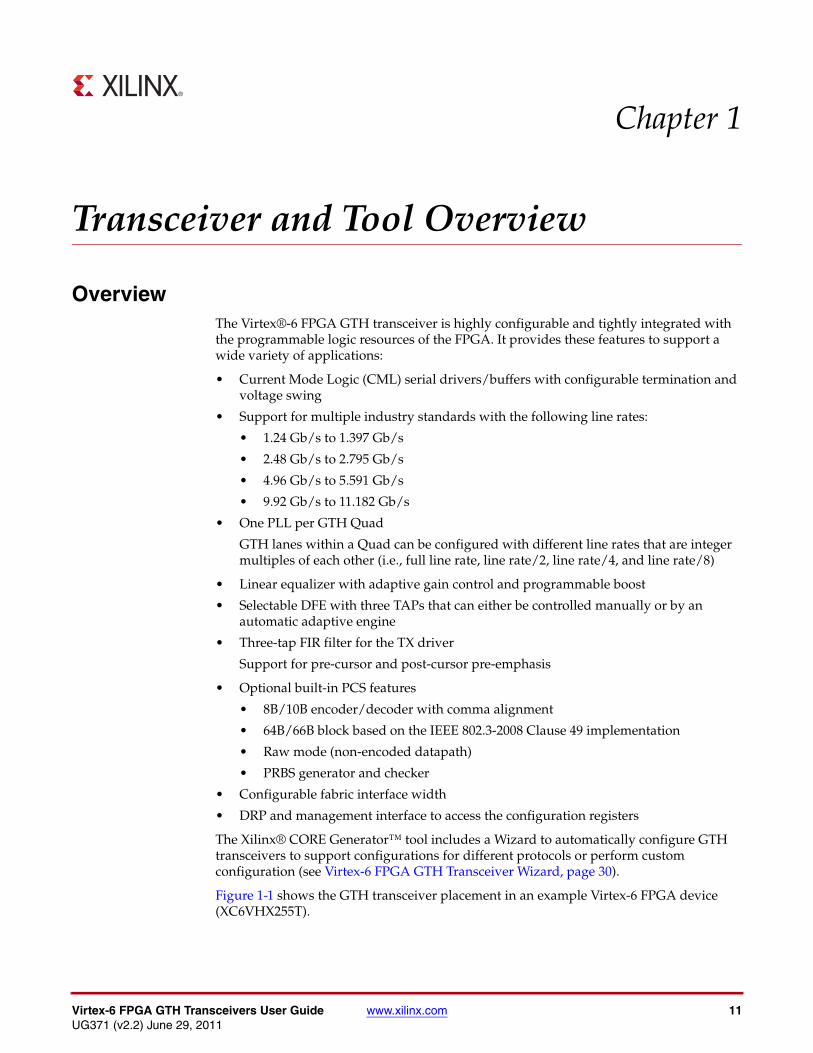
OverviewThe Virtex®-6 FPGA GTH transceiver is highly configurable and tightly integrated with the programmable logic resources of the FPGA. It provides these features to support a wide variety of applications:
• Current Mode Logic (CML) serial drivers/buffers with configurable termination and voltage swing
• Support for multiple industry standards with the following line rates:
• 1.24 Gb/s to 1.397 Gb/s
• 2.48 Gb/s to 2.795 Gb/s
• 4.96 Gb/s to 5.591 Gb/s
• 9.92 Gb/s to 11.182 Gb/s
• One PLL per GTH Quad
GTH lanes within a Quad can be configured with different line rates that are integer multiples of each other (i.e., full line rate, line rate/2, line rate/4, and line rate/8)
• Linear equalizer with adaptive gain control and programmable boost
• Selectable DFE with three TAPs that can either be controlled manually or by an automatic adaptive engine
• Three-tap FIR filter for the TX driver
Support for pre-cursor and post-cursor pre-emphasis
• Optional built-in PCS features
• 8B/10B encoder/decoder with comma alignment
• 64B/66B block based on the IEEE 802.3-2008 Clause 49 implementation
• Raw mode (non-encoded datapath)
• PRBS generator and checker
• Configurable fabric interface width
• DRP and management interface to access the configuration registers
The Xilinx® CORE Generator™ tool includes a Wizard to automatically configure GTH transceivers to support configurations for different protocols or perform custom configuration (see Virtex-6 FPGA GTH Transceiver Wizard, page 30).
Figure 1-1 shows the GTH transceiver placement in an example Virtex-6 FPGA device (XC6VHX255T).

12 www.xilinx.com Virtex-6 FPGA GTH Transceivers User GuideUG371 (v2.2) June 29, 2011
Chapter 1: Transceiver and Tool Overview
Notes relevant to Figure 1-1:
1. This figure does not illustrate exact size, location, or scale of the functional blocks to each other. It does show the correct number of available resources.
2. To improve clarity, this figure does not show the CLB, DSP, and block RAM columns.
X-Ref Target - Figure 1-1
Figure 1-1: GTH Transceiver Inside the Virtex-6 XC6VHX255T FPGA
MMCM
GTHE1_QUADColumn
GTXE1Column
GTXE1_X0Y10
GTXE1_X0Y9
GTXE1_X0Y8
GTXE1_X0Y7
GTXE1_X0Y6
GTXE1_X0Y5
GTXE1_X0Y4
GTXE1_X0Y3
GTXE1_X0Y2
GTXE1_X0Y1
GTXE1_X0Y0
GTXE1_X0Y11
GTHE1_QUAD_X0Y2
GTHE1_QUAD_X0Y1
GTHE1_QUAD_X0Y0
GTHE1_QUADColumn
GTXE1Column
GTXE1_X1Y10
GTXE1_X1Y9
GTXE1_X1Y8
GTXE1_X1Y7
GTXE1_X1Y6
GTXE1_X1Y5
GTXE1_X1Y4
GTXE1_X1Y3
GTXE1_X1Y2
GTXE1_X1Y1
GTXE1_X1Y0
GTXE1_X1Y11
GTHE1_QUAD_X1Y2
GTHE1_QUAD_X1Y1
GTHE1_QUAD_X1Y0
MMCM
MMCM
MMCM
MMCM
MMCM
I/OCollumn
Configuration
I/OCollumn
PCIExpress
PCIExpress
EthernetMAC
EthernetMAC
MMCM
MMCM
MMCM
MMCM
MMCM
MMCM
UG371_c1_01_090810

Virtex-6 FPGA GTH Transceivers User Guide www.xilinx.com 13UG371 (v2.2) June 29, 2011
Overview
Figure 1-2 shows a diagram of the GTH Quad, containing four GTH transceivers, a PLL, and shared resources for controlling and initializing the Quad.
X-Ref Target - Figure 1-2
Figure 1-2: GTH Quad Block Diagram
UG371_c1_02_120809
GTH3
Fabric Data,Control, andClock forGTH3
PCSPCS to Fabric
Interface
TX3
RX3
GTH2
Fabric Data,Control, andClock forGTH2
PCSPCS to Fabric
Interface
TX2
RX2
GTH1
Fabric Data,Control, andClock forGTH1
PCSPCS to Fabric
Interface
TX1
RX1
GTH0
GTH QUAD
Fabric Data,Control, andClock forGTH0
PCSPCS to Fabric
Interface
TX0
RX0
PMA
PMA
PMA
PMA
PLLReset and
Power-DownControls
DRP Interface
ManagementInterface Unit
REFCLK

14 www.xilinx.com Virtex-6 FPGA GTH Transceivers User GuideUG371 (v2.2) June 29, 2011
Chapter 1: Transceiver and Tool Overview
Port and Attribute SummaryThis section contains alphabetical tables of power pins, ports, and attributes for the GTH transceiver.
For all ports mentioned in this guide:
• Names that end with 0 are for the GTH0 transceiver on the Quad
• Names that end with 1 are for the GTH1 transceiver on the Quad
• Names that end with 2 are for the GTH2 transceiver on the Quad
• Names that end with 3 are for the GTH3 transceiver on the Quad
• Port names that do not end with 0, 1, 2 or 3 are shared.
For all attributes mentioned in this guide:
• Names that end with LANE0 are for the GTH0 transceiver on the Quad
• Names that end with LANE1 are for the GTH1 transceiver on the Quad
• Names that end with LANE2 are for the GTH2 transceiver on the Quad
• Names that end with LANE3 are for the GTH3 transceiver on the Quad
• Attribute names that do not end with LANE0, LANE1, LANE2 or LANE3 are shared.
Table 1-1 lists alphabetically the signal names and directions of the GTH transceiver analog pins..
Table 1-1: GTH Analog Pin Summary
Pin Dir
MGTHAGND_[L,R](1) In
MGTHAVCC_[L,R](1) In
MGTHAVCCPLL_[L,R](1) In
MGTHAVCCRX_[L,R](1) In
MGTHAVTT_[L,R](1) In
MGTRBIAS In
MGTREFCLKP/MGTREFCLKN In
MGTTXP0/MGTTXN0
OutMGTTXP1/MGTTXN1
MGTTXP2/MGTTXN2
MGTTXP3/MGTTXN3
MGTRXP0/MGTRXN0
InMGTRXP1/MGTRXN1
MGTRXP2/MGTRXN2
MGTRXP3/MGTRXN3
Notes: 1. These are power supply pins.

Virtex-6 FPGA GTH Transceivers User Guide www.xilinx.com 15UG371 (v2.2) June 29, 2011
Port and Attribute Summary
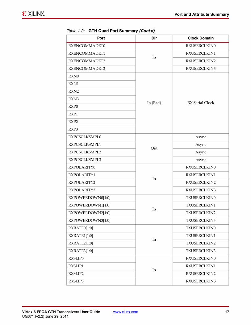
Table 1-2 lists alphabetically the signal names, directions, and clock domain of the GTH Quad ports.
Table 1-2: GTH Quad Port Summary
Port Dir Clock Domain
DADDR[15:0] In DCLK
DCLK In N/A
DEN In DCLK
DFETRAINCTRL0
In DCLKDFETRAINCTRL1
DFETRAINCTRL2
DFETRAINCTRL3
DI[15:0] In DCLK
DISABLEDRP In DCLK
DRPDO[15:0] Out DCLK
DRDY Out DCLK
DWE In DCLK
GTHINIT In DCLK
GTHINITDONE Out DCLK
GTHRESET In DCLK
GTHX2LANE01 In Async
GTHX2LANE23 In Async
GTHX4LANE In Async
MGMTPCSLANESEL[3:0] In DCLK
MGMTPCSMMDADDR[4:0] In DCLK
MGMTPCSRDACK Out DCLK
MGMTPCSRDDATA[15:0] Out DCLK
MGMTPCSREGADDR[15:0] In DCLK
MGMTPCSREGRD In DCLK
MGMTPCSREGWR In DCLK
MGMTPCSWRDATA[15:0] In DCLK
PLLPCSCLKDIV[5:0] In DCLK
PLLREFCLKSEL[2:0] In DCLK

16 www.xilinx.com Virtex-6 FPGA GTH Transceivers User GuideUG371 (v2.2) June 29, 2011
Chapter 1: Transceiver and Tool Overview
POWERDOWN0
In
TXUSERCLKIN0
POWERDOWN1 TXUSERCLKIN1
POWERDOWN2 TXUSERCLKIN2
POWERDOWN3 TXUSERCLKIN3
REFCLK In N/A
RXBUFRESET0
In
RXUSERCLKIN0
RXBUFRESET1 RXUSERCLKIN1
RXBUFRESET2 RXUSERCLKIN2
RXBUFRESET3 RXUSERCLKIN3
RXCODEERR0[7:0]
Out
RXUSERCLKIN0
RXCODEERR1[7:0] RXUSERCLKIN1
RXCODEERR2[7:0] RXUSERCLKIN2
RXCODEERR3[7:0] RXUSERCLKIN3
RXCTRL0[7:0]
Out
RXUSERCLKIN0
RXCTRL1[7:0] RXUSERCLKIN1
RXCTRL2[7:0] RXUSERCLKIN2
RXCTRL3[7:0] RXUSERCLKIN3
RXCTRLACK0
Out
TXUSERCLKIN0
RXCTRLACK1 TXUSERCLKIN1
RXCTRLACK2 TXUSERCLKIN2
RXCTRLACK3 TXUSERCLKIN3
RXDATA0[63:0]
Out
RXUSERCLKIN0
RXDATA1[63:0] RXUSERCLKIN1
RXDATA2[63:0] RXUSERCLKIN2
RXDATA3[63:0] RXUSERCLKIN3
RXDATATAP0
Out
Async
RXDATATAP1 Async
RXDATATAP2 Async
RXDATATAP3 Async
RXDISPERR0[7:0]
Out
RXUSERCLKIN0
RXDISPERR1[7:0] RXUSERCLKIN1
RXDISPERR2[7:0] RXUSERCLKIN2
RXDISPERR3[7:0] RXUSERCLKIN3
Table 1-2: GTH Quad Port Summary (Cont’d)
Port Dir Clock Domain
Virtex-6 FPGA GTH Transceivers User Guide www.xilinx.com 17UG371 (v2.2) June 29, 2011
Port and Attribute Summary
RXENCOMMADET0
In
RXUSERCLKIN0
RXENCOMMADET1 RXUSERCLKIN1
RXENCOMMADET2 RXUSERCLKIN2
RXENCOMMADET3 RXUSERCLKIN3
RXN0
In (Pad) RX Serial Clock
RXN1
RXN2
RXN3
RXP0
RXP1
RXP2
RXP3
RXPCSCLKSMPL0
Out
Async
RXPCSCLKSMPL1 Async
RXPCSCLKSMPL2 Async
RXPCSCLKSMPL3 Async
RXPOLARITY0
In
RXUSERCLKIN0
RXPOLARITY1 RXUSERCLKIN1
RXPOLARITY2 RXUSERCLKIN2
RXPOLARITY3 RXUSERCLKIN3
RXPOWERDOWN0[1:0]
In
TXUSERCLKIN0
RXPOWERDOWN1[1:0] TXUSERCLKIN1
RXPOWERDOWN2[1:0] TXUSERCLKIN2
RXPOWERDOWN3[1:0] TXUSERCLKIN3
RXRATE0[1:0]
In
TXUSERCLKIN0
RXRATE1[1:0] TXUSERCLKIN1
RXRATE2[1:0] TXUSERCLKIN2
RXRATE3[1:0] TXUSERCLKIN3
RXSLIP0
In
RXUSERCLKIN0
RXSLIP1 RXUSERCLKIN1
RXSLIP2 RXUSERCLKIN2
RXSLIP3 RXUSERCLKIN3
Table 1-2: GTH Quad Port Summary (Cont’d)
Port Dir Clock Domain

18 www.xilinx.com Virtex-6 FPGA GTH Transceivers User GuideUG371 (v2.2) June 29, 2011
Chapter 1: Transceiver and Tool Overview
RXUSERCLKIN0
In N/ARXUSERCLKIN1
RXUSERCLKIN2
RXUSERCLKIN3
RXUSERCLKOUT0
Out N/ARXUSERCLKOUT1
RXUSERCLKOUT2
RXUSERCLKOUT3
RXVALID0[7:0]
Out
RXUSERCLKIN0
RXVALID1[7:0] RXUSERCLKIN1
RXVALID2[7:0] RXUSERCLKIN2
RXVALID3[7:0] RXUSERCLKIN3
SAMPLERATE0[2:0]
In
TXUSERCLKIN0
SAMPLERATE1[2:0] TXUSERCLKIN1
SAMPLERATE2[2:0] TXUSERCLKIN2
SAMPLERATE3[2:0] TXUSERCLKIN3
TSTPATH Out Async
TSTREFCLKFAB Out N/A
TSTREFCLKOUT Out N/A
TXBUFRESET0
In
TXUSERCLKIN0
TXBUFRESET1 TXUSERCLKIN1
TXBUFRESET2 TXUSERCLKIN2
TXBUFRESET3 TXUSERCLKIN3
TXCTRL0[7:0]
In
TXUSERCLKIN0
TXCTRL1[7:0] TXUSERCLKIN1
TXCTRL2[7:0] TXUSERCLKIN2
TXCTRL3[7:0] TXUSERCLKIN3
TXCTRLACK0
Out
TXUSERCLKIN0
TXCTRLACK1 TXUSERCLKIN1
TXCTRLACK2 TXUSERCLKIN2
TXCTRLACK3 TXUSERCLKIN3
Table 1-2: GTH Quad Port Summary (Cont’d)
Port Dir Clock Domain

Virtex-6 FPGA GTH Transceivers User Guide www.xilinx.com 19UG371 (v2.2) June 29, 2011
Port and Attribute Summary
TXDATA0[63:0]
In
TXUSERCLKIN0
TXDATA1[63:0] TXUSERCLKIN1
TXDATA2[63:0] TXUSERCLKIN2
TXDATA3[63:0] TXUSERCLKIN3
TXDATAMSB0[7:0]
In
TXUSERCLKIN0
TXDATAMSB1[7:0] TXUSERCLKIN1
TXDATAMSB2[7:0] TXUSERCLKIN2
TXDATAMSB3[7:0] TXUSERCLKIN3
TXDATATAP10
Out
Async
TXDATATAP11 Async
TXDATATAP12 Async
TXDATATAP13 Async
TXDATATAP20
Out
Async
TXDATATAP21 Async
TXDATATAP22 Async
TXDATATAP23 Async
TXDEEMPH0
In
TXUSERCLKIN0
TXDEEMPH1 TXUSERCLKIN1
TXDEEMPH2 TXUSERCLKIN2
TXDEEMPH3 TXUSERCLKIN3
TXMARGIN0[2:0]
In
TXUSERCLKIN0
TXMARGIN1[2:0] TXUSERCLKIN1
TXMARGIN2[2:0] TXUSERCLKIN2
TXMARGIN3[2:0] TXUSERCLKIN3
TXN0
Out
(Pad)TX Serial Clock
TXN1
TXN2
TXN3
TXP0
TXP1
TXP2
TXP3
Table 1-2: GTH Quad Port Summary (Cont’d)
Port Dir Clock Domain

20 www.xilinx.com Virtex-6 FPGA GTH Transceivers User GuideUG371 (v2.2) June 29, 2011
Chapter 1: Transceiver and Tool Overview
The ports in Table 1-3 are part of the GTH IBUFDS primitive.
TXPCSCLKSMPL0
Out
Async
TXPCSCLKSMPL1 Async
TXPCSCLKSMPL2 Async
TXPCSCLKSMPL3 Async
TXPOWERDOWN0[1:0]
In
TXUSERCLKIN0
TXPOWERDOWN1[1:0] TXUSERCLKIN1
TXPOWERDOWN2[1:0] TXUSERCLKIN2
TXPOWERDOWN3[1:0] TXUSERCLKIN3
TXRATE0[1:0]
In
TXUSERCLKIN0
TXRATE1[1:0] TXUSERCLKIN1
TXRATE2[1:0] TXUSERCLKIN2
TXRATE3[1:0] TXUSERCLKIN3
TXUSERCLKIN0
In N/ATXUSERCLKIN1
TXUSERCLKIN2
TXUSERCLKIN3
TXUSERCLKOUT0
Out N/ATXUSERCLKOUT1
TXUSERCLKOUT2
TXUSERCLKOUT3
Table 1-3: GTH Reference Clock (IBUFDS_GTHE1) Port Summary
Port Dir Clock Domain
I In Async
IB In Async
O Out Async
Table 1-2: GTH Quad Port Summary (Cont’d)
Port Dir Clock Domain

Virtex-6 FPGA GTH Transceivers User Guide www.xilinx.com 21UG371 (v2.2) June 29, 2011
Port and Attribute Summary
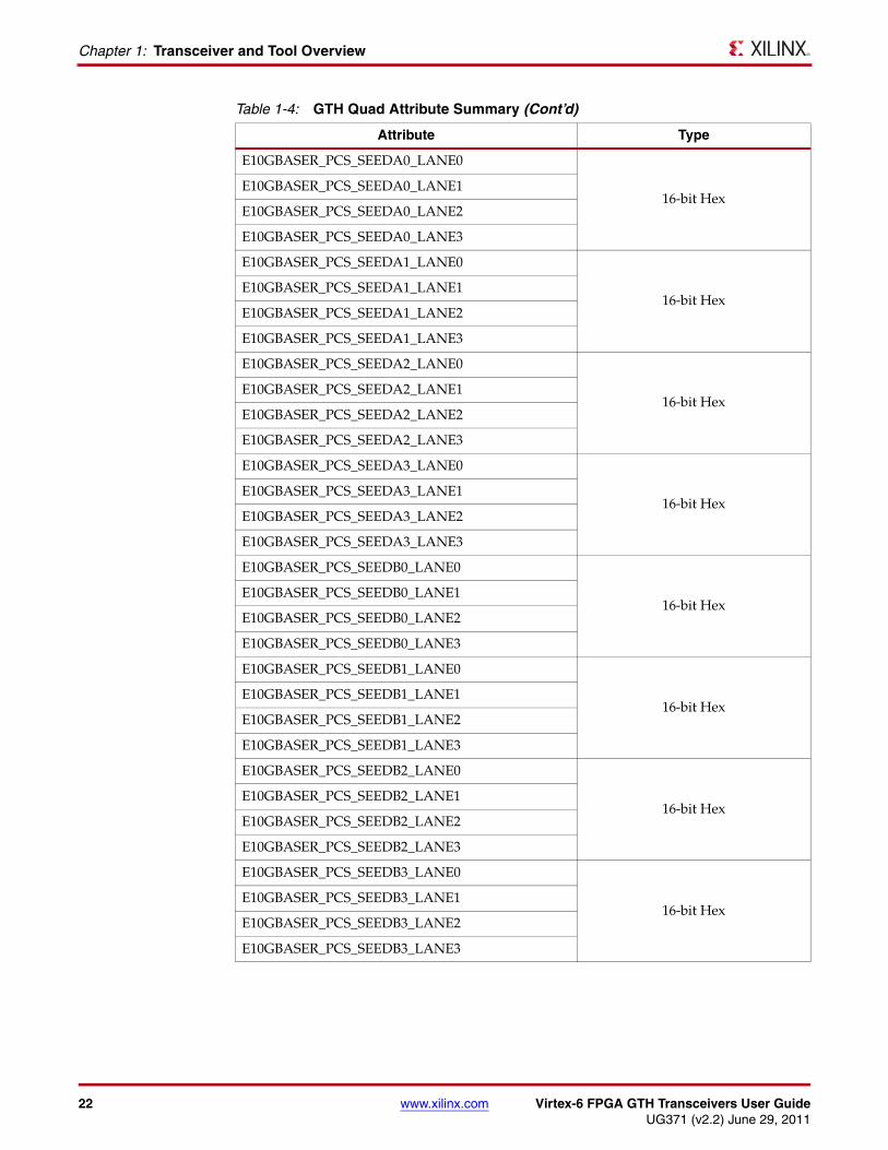
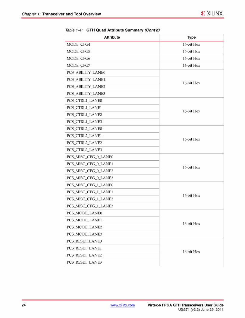
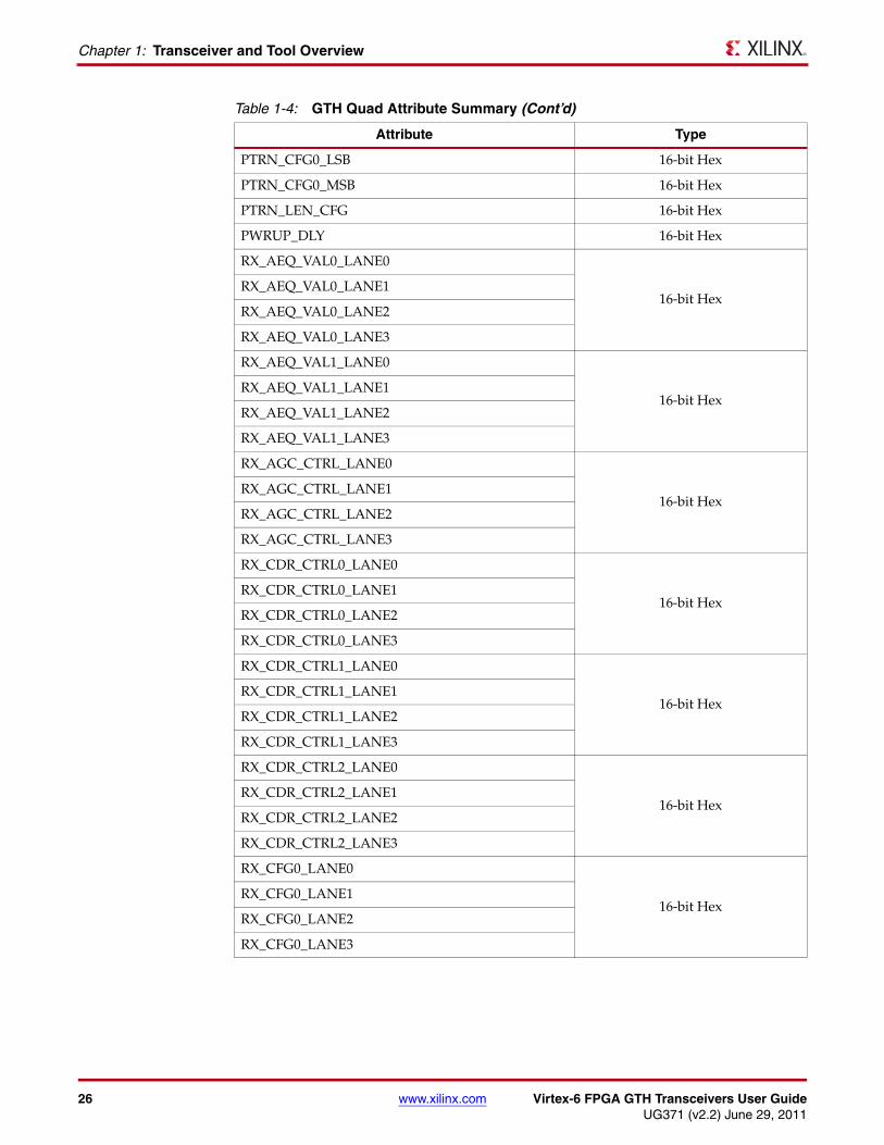
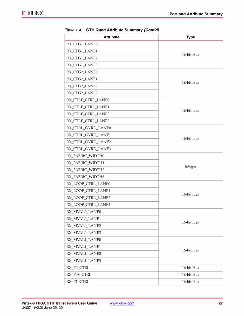
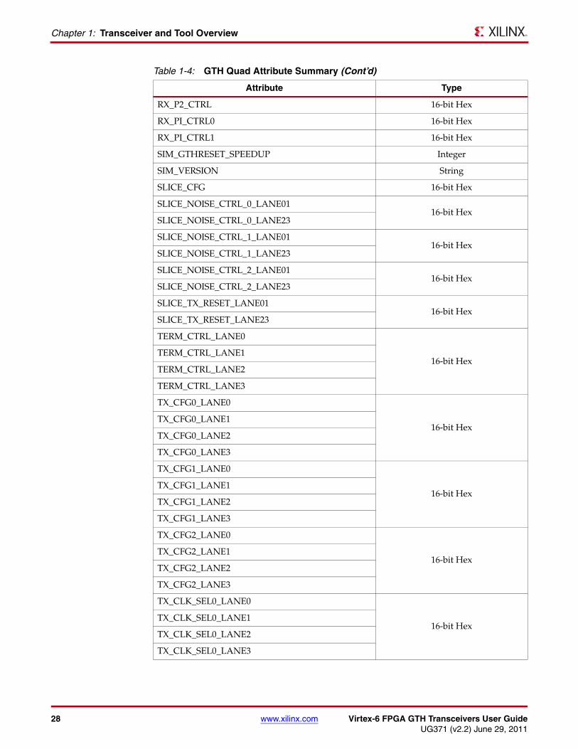
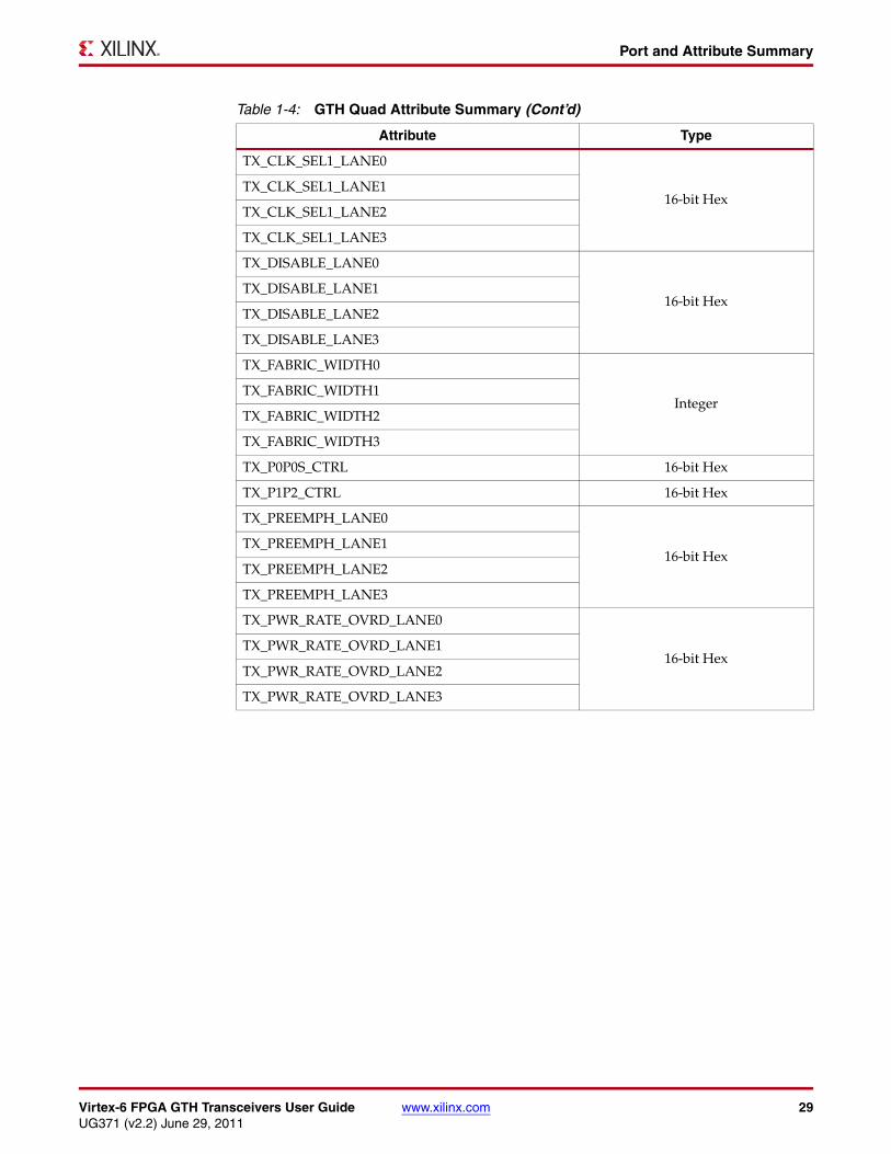
Table 1-4 lists alphabetically the attribute names and type of the GTH Quad attributes..
Table 1-4: GTH Quad Attribute Summary
Attribute Type
BER_CONST_PTRN0 16-bit Hex
BER_CONST_PTRN1 16-bit Hex
BUFFER_CONFIG_LANE0
16-bit HexBUFFER_CONFIG_LANE1
BUFFER_CONFIG_LANE2
BUFFER_CONFIG_LANE3
DFE_TRAIN_CTRL_LANE0
16-bit HexDFE_TRAIN_CTRL_LANE1
DFE_TRAIN_CTRL_LANE2
DFE_TRAIN_CTRL_LANE3
DLL_CFG0 16-bit Hex
DLL_CFG1 16-bit Hex
E10GBASEKR_LD_COEFF_UPD_LANE0
16-bit HexE10GBASEKR_LD_COEFF_UPD_LANE1
E10GBASEKR_LD_COEFF_UPD_LANE2
E10GBASEKR_LD_COEFF_UPD_LANE3
E10GBASEKR_LP_COEFF_UPD_LANE0
16-bit HexE10GBASEKR_LP_COEFF_UPD_LANE1
E10GBASEKR_LP_COEFF_UPD_LANE2
E10GBASEKR_LP_COEFF_UPD_LANE3
E10GBASEKR_PMA_CTRL_LANE0
16-bit HexE10GBASEKR_PMA_CTRL_LANE1
E10GBASEKR_PMA_CTRL_LANE2
E10GBASEKR_PMA_CTRL_LANE3
E10GBASEKX_CTRL_LANE0
16-bit HexE10GBASEKX_CTRL_LANE1
E10GBASEKX_CTRL_LANE2
E10GBASEKX_CTRL_LANE3
E10GBASER_PCS_CFG_LANE0
16-bit HexE10GBASER_PCS_CFG_LANE1
E10GBASER_PCS_CFG_LANE2
E10GBASER_PCS_CFG_LANE3
22 www.xilinx.com Virtex-6 FPGA GTH Transceivers User GuideUG371 (v2.2) June 29, 2011
Chapter 1: Transceiver and Tool Overview
E10GBASER_PCS_SEEDA0_LANE0
16-bit HexE10GBASER_PCS_SEEDA0_LANE1
E10GBASER_PCS_SEEDA0_LANE2
E10GBASER_PCS_SEEDA0_LANE3
E10GBASER_PCS_SEEDA1_LANE0
16-bit HexE10GBASER_PCS_SEEDA1_LANE1
E10GBASER_PCS_SEEDA1_LANE2
E10GBASER_PCS_SEEDA1_LANE3
E10GBASER_PCS_SEEDA2_LANE0
16-bit HexE10GBASER_PCS_SEEDA2_LANE1
E10GBASER_PCS_SEEDA2_LANE2
E10GBASER_PCS_SEEDA2_LANE3
E10GBASER_PCS_SEEDA3_LANE0
16-bit HexE10GBASER_PCS_SEEDA3_LANE1
E10GBASER_PCS_SEEDA3_LANE2
E10GBASER_PCS_SEEDA3_LANE3
E10GBASER_PCS_SEEDB0_LANE0
16-bit HexE10GBASER_PCS_SEEDB0_LANE1
E10GBASER_PCS_SEEDB0_LANE2
E10GBASER_PCS_SEEDB0_LANE3
E10GBASER_PCS_SEEDB1_LANE0
16-bit HexE10GBASER_PCS_SEEDB1_LANE1
E10GBASER_PCS_SEEDB1_LANE2
E10GBASER_PCS_SEEDB1_LANE3
E10GBASER_PCS_SEEDB2_LANE0
16-bit HexE10GBASER_PCS_SEEDB2_LANE1
E10GBASER_PCS_SEEDB2_LANE2
E10GBASER_PCS_SEEDB2_LANE3
E10GBASER_PCS_SEEDB3_LANE0
16-bit HexE10GBASER_PCS_SEEDB3_LANE1
E10GBASER_PCS_SEEDB3_LANE2
E10GBASER_PCS_SEEDB3_LANE3
Table 1-4: GTH Quad Attribute Summary (Cont’d)
Attribute Type

Virtex-6 FPGA GTH Transceivers User Guide www.xilinx.com 23UG371 (v2.2) June 29, 2011
Port and Attribute Summary
E10GBASER_PCS_TEST_CTRL_LANE0
16-bit HexE10GBASER_PCS_TEST_CTRL_LANE1
E10GBASER_PCS_TEST_CTRL_LANE2
E10GBASER_PCS_TEST_CTRL_LANE3
E10GBASEX_PCS_TSTCTRL_LANE0
16-bit HexE10GBASEX_PCS_TSTCTRL_LANE1
E10GBASEX_PCS_TSTCTRL_LANE2
E10GBASEX_PCS_TSTCTRL_LANE3
GLBL0_NOISE_CTRL 16-bit Hex
GLBL_AMON_SEL 16-bit Hex
GLBL_DMON_SEL 16-bit Hex
GLBL_PWR_CTRL 16-bit Hex
GTH_CFG_PWRUP_LANE0
1-bit BinaryGTH_CFG_PWRUP_LANE1
GTH_CFG_PWRUP_LANE2
GTH_CFG_PWRUP_LANE3
LANE_AMON_SEL 16-bit Hex
LANE_DMON_SEL 16-bit Hex
LANE_LNK_CFGOVRD 16-bit Hex
LANE_PWR_CTRL_LANE0
16-bit HexLANE_PWR_CTRL_LANE1
LANE_PWR_CTRL_LANE2
LANE_PWR_CTRL_LANE3
LNK_TRN_CFG_LANE0
16-bit HexLNK_TRN_CFG_LANE1
LNK_TRN_CFG_LANE2
LNK_TRN_CFG_LANE3
LNK_TRN_COEFF_REQ_LANE0
16-bit HexLNK_TRN_COEFF_REQ_LANE1
LNK_TRN_COEFF_REQ_LANE2
LNK_TRN_COEFF_REQ_LANE3
MISC_CFG 16-bit Hex
MODE_CFG1 16-bit Hex
MODE_CFG2 16-bit Hex
MODE_CFG3 16-bit Hex
Table 1-4: GTH Quad Attribute Summary (Cont’d)
Attribute Type
24 www.xilinx.com Virtex-6 FPGA GTH Transceivers User GuideUG371 (v2.2) June 29, 2011
Chapter 1: Transceiver and Tool Overview
MODE_CFG4 16-bit Hex
MODE_CFG5 16-bit Hex
MODE_CFG6 16-bit Hex
MODE_CFG7 16-bit Hex
PCS_ABILITY_LANE0
16-bit HexPCS_ABILITY_LANE1
PCS_ABILITY_LANE2
PCS_ABILITY_LANE3
PCS_CTRL1_LANE0
16-bit HexPCS_CTRL1_LANE1
PCS_CTRL1_LANE2
PCS_CTRL1_LANE3
PCS_CTRL2_LANE0
16-bit HexPCS_CTRL2_LANE1
PCS_CTRL2_LANE2
PCS_CTRL2_LANE3
PCS_MISC_CFG_0_LANE0
16-bit HexPCS_MISC_CFG_0_LANE1
PCS_MISC_CFG_0_LANE2
PCS_MISC_CFG_0_LANE3
PCS_MISC_CFG_1_LANE0
16-bit HexPCS_MISC_CFG_1_LANE1
PCS_MISC_CFG_1_LANE2
PCS_MISC_CFG_1_LANE3
PCS_MODE_LANE0
16-bit HexPCS_MODE_LANE1
PCS_MODE_LANE2
PCS_MODE_LANE3
PCS_RESET_LANE0
16-bit HexPCS_RESET_LANE1
PCS_RESET_LANE2
PCS_RESET_LANE3
Table 1-4: GTH Quad Attribute Summary (Cont’d)
Attribute Type

Virtex-6 FPGA GTH Transceivers User Guide www.xilinx.com 25UG371 (v2.2) June 29, 2011
Port and Attribute Summary
PCS_RESET_1_LANE0
16-bit HexPCS_RESET_1_LANE1
PCS_RESET_1_LANE2
PCS_RESET_1_LANE3
PCS_TYPE_LANE0
16-bit HexPCS_TYPE_LANE1
PCS_TYPE_LANE2
PCS_TYPE_LANE3
PLL_CFG0 16-bit Hex
PLL_CFG1 16-bit Hex
PLL_CFG2 16-bit Hex
PMA_CTRL1_LANE0
16-bit HexPMA_CTRL1_LANE1
PMA_CTRL1_LANE2
PMA_CTRL1_LANE3
PMA_CTRL2_LANE0
16-bit HexPMA_CTRL2_LANE1
PMA_CTRL2_LANE2
PMA_CTRL2_LANE3
PMA_LPBK_CTRL_LANE0
16-bit HexPMA_LPBK_CTRL_LANE1
PMA_LPBK_CTRL_LANE2
PMA_LPBK_CTRL_LANE3
PRBS_BER_CFG0_LANE0
16-bit HexPRBS_BER_CFG0_LANE1
PRBS_BER_CFG0_LANE2
PRBS_BER_CFG0_LANE3
PRBS_BER_CFG1_LANE0
16-bit HexPRBS_BER_CFG1_LANE1
PRBS_BER_CFG1_LANE2
PRBS_BER_CFG1_LANE3
PRBS_CFG_LANE0
16-bit HexPRBS_CFG_LANE1
PRBS_CFG_LANE2
PRBS_CFG_LANE3
Table 1-4: GTH Quad Attribute Summary (Cont’d)
Attribute Type
26 www.xilinx.com Virtex-6 FPGA GTH Transceivers User GuideUG371 (v2.2) June 29, 2011
Chapter 1: Transceiver and Tool Overview
PTRN_CFG0_LSB 16-bit Hex
PTRN_CFG0_MSB 16-bit Hex
PTRN_LEN_CFG 16-bit Hex
PWRUP_DLY 16-bit Hex
RX_AEQ_VAL0_LANE0
16-bit HexRX_AEQ_VAL0_LANE1
RX_AEQ_VAL0_LANE2
RX_AEQ_VAL0_LANE3
RX_AEQ_VAL1_LANE0
16-bit HexRX_AEQ_VAL1_LANE1
RX_AEQ_VAL1_LANE2
RX_AEQ_VAL1_LANE3
RX_AGC_CTRL_LANE0
16-bit HexRX_AGC_CTRL_LANE1
RX_AGC_CTRL_LANE2
RX_AGC_CTRL_LANE3
RX_CDR_CTRL0_LANE0
16-bit HexRX_CDR_CTRL0_LANE1
RX_CDR_CTRL0_LANE2
RX_CDR_CTRL0_LANE3
RX_CDR_CTRL1_LANE0
16-bit HexRX_CDR_CTRL1_LANE1
RX_CDR_CTRL1_LANE2
RX_CDR_CTRL1_LANE3
RX_CDR_CTRL2_LANE0
16-bit HexRX_CDR_CTRL2_LANE1
RX_CDR_CTRL2_LANE2
RX_CDR_CTRL2_LANE3
RX_CFG0_LANE0
16-bit HexRX_CFG0_LANE1
RX_CFG0_LANE2
RX_CFG0_LANE3
Table 1-4: GTH Quad Attribute Summary (Cont’d)
Attribute Type
Virtex-6 FPGA GTH Transceivers User Guide www.xilinx.com 27UG371 (v2.2) June 29, 2011
Port and Attribute Summary
RX_CFG1_LANE0
16-bit HexRX_CFG1_LANE1
RX_CFG1_LANE2
RX_CFG1_LANE3
RX_CFG2_LANE0
16-bit HexRX_CFG2_LANE1
RX_CFG2_LANE2
RX_CFG2_LANE3
RX_CTLE_CTRL_LANE0
16-bit HexRX_CTLE_CTRL_LANE1
RX_CTLE_CTRL_LANE2
RX_CTLE_CTRL_LANE3
RX_CTRL_OVRD_LANE0
16-bit HexRX_CTRL_OVRD_LANE1
RX_CTRL_OVRD_LANE2
RX_CTRL_OVRD_LANE3
RX_FABRIC_WIDTH0
IntegerRX_FABRIC_WIDTH1
RX_FABRIC_WIDTH2
RX_FABRIC_WIDTH3
RX_LOOP_CTRL_LANE0
16-bit HexRX_LOOP_CTRL_LANE1
RX_LOOP_CTRL_LANE2
RX_LOOP_CTRL_LANE3
RX_MVAL0_LANE0
16-bit HexRX_MVAL0_LANE1
RX_MVAL0_LANE2
RX_MVAL0_LANE3
RX_MVAL1_LANE0
16-bit HexRX_MVAL1_LANE1
RX_MVAL1_LANE2
RX_MVAL1_LANE3
RX_P0_CTRL 16-bit Hex
RX_P0S_CTRL 16-bit Hex
RX_P1_CTRL 16-bit Hex
Table 1-4: GTH Quad Attribute Summary (Cont’d)
Attribute Type
28 www.xilinx.com Virtex-6 FPGA GTH Transceivers User GuideUG371 (v2.2) June 29, 2011
Chapter 1: Transceiver and Tool Overview
RX_P2_CTRL 16-bit Hex
RX_PI_CTRL0 16-bit Hex
RX_PI_CTRL1 16-bit Hex
SIM_GTHRESET_SPEEDUP Integer
SIM_VERSION String
SLICE_CFG 16-bit Hex
SLICE_NOISE_CTRL_0_LANE0116-bit Hex
SLICE_NOISE_CTRL_0_LANE23
SLICE_NOISE_CTRL_1_LANE0116-bit Hex
SLICE_NOISE_CTRL_1_LANE23
SLICE_NOISE_CTRL_2_LANE0116-bit Hex
SLICE_NOISE_CTRL_2_LANE23
SLICE_TX_RESET_LANE0116-bit Hex
SLICE_TX_RESET_LANE23
TERM_CTRL_LANE0
16-bit HexTERM_CTRL_LANE1
TERM_CTRL_LANE2
TERM_CTRL_LANE3
TX_CFG0_LANE0
16-bit HexTX_CFG0_LANE1
TX_CFG0_LANE2
TX_CFG0_LANE3
TX_CFG1_LANE0
16-bit HexTX_CFG1_LANE1
TX_CFG1_LANE2
TX_CFG1_LANE3
TX_CFG2_LANE0
16-bit HexTX_CFG2_LANE1
TX_CFG2_LANE2
TX_CFG2_LANE3
TX_CLK_SEL0_LANE0
16-bit HexTX_CLK_SEL0_LANE1
TX_CLK_SEL0_LANE2
TX_CLK_SEL0_LANE3
Table 1-4: GTH Quad Attribute Summary (Cont’d)
Attribute Type
Virtex-6 FPGA GTH Transceivers User Guide www.xilinx.com 29UG371 (v2.2) June 29, 2011
Port and Attribute Summary
TX_CLK_SEL1_LANE0
16-bit HexTX_CLK_SEL1_LANE1
TX_CLK_SEL1_LANE2
TX_CLK_SEL1_LANE3
TX_DISABLE_LANE0
16-bit HexTX_DISABLE_LANE1
TX_DISABLE_LANE2
TX_DISABLE_LANE3
TX_FABRIC_WIDTH0
IntegerTX_FABRIC_WIDTH1
TX_FABRIC_WIDTH2
TX_FABRIC_WIDTH3
TX_P0P0S_CTRL 16-bit Hex
TX_P1P2_CTRL 16-bit Hex
TX_PREEMPH_LANE0
16-bit HexTX_PREEMPH_LANE1
TX_PREEMPH_LANE2
TX_PREEMPH_LANE3
TX_PWR_RATE_OVRD_LANE0
16-bit HexTX_PWR_RATE_OVRD_LANE1
TX_PWR_RATE_OVRD_LANE2
TX_PWR_RATE_OVRD_LANE3
Table 1-4: GTH Quad Attribute Summary (Cont’d)
Attribute Type
30 www.xilinx.com Virtex-6 FPGA GTH Transceivers User GuideUG371 (v2.2) June 29, 2011
Chapter 1: Transceiver and Tool Overview
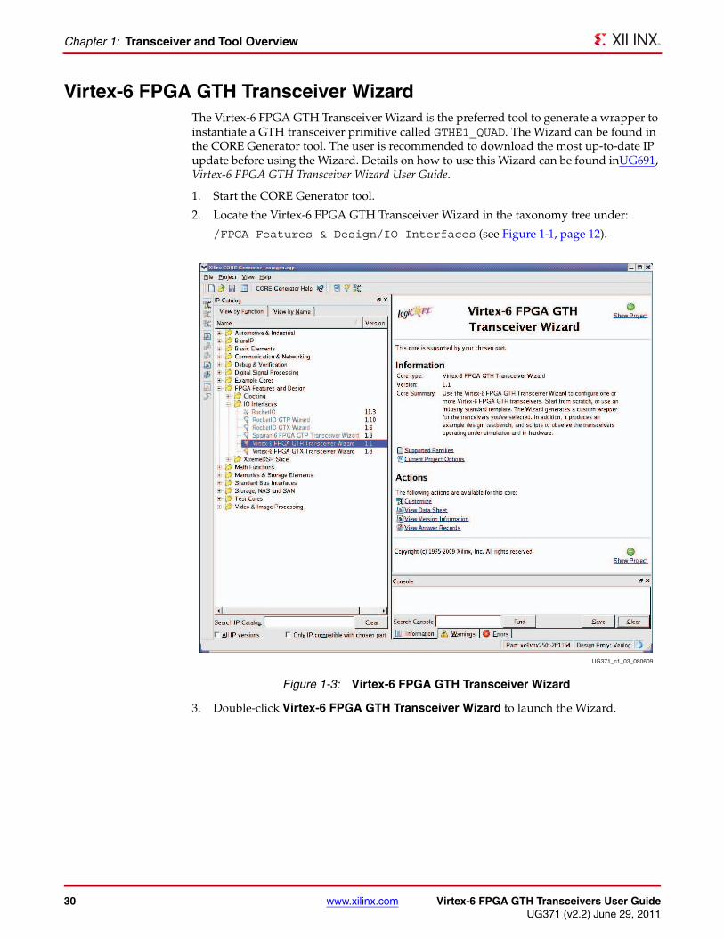
Virtex-6 FPGA GTH Transceiver WizardThe Virtex-6 FPGA GTH Transceiver Wizard is the preferred tool to generate a wrapper to instantiate a GTH transceiver primitive called GTHE1_QUAD. The Wizard can be found in the CORE Generator tool. The user is recommended to download the most up-to-date IP update before using the Wizard. Details on how to use this Wizard can be found inUG691, Virtex-6 FPGA GTH Transceiver Wizard User Guide.
1. Start the CORE Generator tool.
2. Locate the Virtex-6 FPGA GTH Transceiver Wizard in the taxonomy tree under:
/FPGA Features & Design/IO Interfaces (see Figure 1-1, page 12).
3. Double-click Virtex-6 FPGA GTH Transceiver Wizard to launch the Wizard.
X-Ref Target - Figure 1-3
Figure 1-3: Virtex-6 FPGA GTH Transceiver Wizard
UG371_c1_03_080609

Virtex-6 FPGA GTH Transceivers User Guide www.xilinx.com 31UG371 (v2.2) June 29, 2011
Simulation
Simulation
Functional DescriptionFor simulating a design with GTH transceivers, SecureIP libraries must be compiled using the COMPXLIB tool. For more details on SecureIP, COMPXLIB, and setting up the simulation environment, see the Synthesis and Simulation Design Guide, available in the ISE® software documentation, for instructions on how to compile ISE simulation libraries.
Ports and AttributesThere are no simulation-only ports.
The GTHE1_QUAD primitive has attributes intended only for simulation. Table 1-5 lists the simulation-only attributes of the GTHE1_QUAD primitive. The names of these attributes start with SIM_..
Implementation
Functional DescriptionThis section provides the information needed to map Virtex-6 FPGA GTH transceivers instantiated in a design to device resources, including:
• The location of the GTH transceiver on the available device and package combinations.
• The pad numbers of external signals associated with each GTH transceiver.
• How the GTH Quad and clocking resources instantiated in a design are mapped to available locations with a user constraints file (UCF).
It is a common practice to define the location of the GTH Quad early in the design process to ensure correct usage of clock resources and to facilitate signal integrity analysis during board design. The implementation flow facilitates this practice through the use of location constraints in the UCF.
While this section describes how to instantiate GTH clocking components, the details of the different GTH transceiver clocking options are discussed in Reference Clock Distribution and Selection, page 45.
Table 1-5: Simulation Attributes
Attribute Type Description
SIM_GTHRESET_SPEEDUP Integer This attribute shortens the number of DCLK cycles required to finish the GTHRESET sequence during simulation (deassertion of GTHRESET to the assertion of GTHINITDONE).
0: The GTHRESET sequence is simulated with its original duration (standard initialization is approximately 360 µs for a 50 MHz DCLK).1: The GTHRESET cycle time is shortened (fast initialization is approximately 50 µs for a 50 MHz DCLK).
SIM_VERSION Real This attribute selects the simulation version to match different steppings of silicon. The default for this attribute is 1.0.

32 www.xilinx.com Virtex-6 FPGA GTH Transceivers User GuideUG371 (v2.2) June 29, 2011
Chapter 1: Transceiver and Tool Overview
The position of the GTH Quad is specified by an XY coordinate system that describes the column number and its relative position within that column. In the Virtex-6 HXT device, there are packages with all the GTH Quads located in a single column along one side of the die, and other packages with all GTH Quads located on both the left column (X0) and right column (X1) of the die.
There are two ways to create a UCF for designs that use the GTH transceiver. The preferred method is to use the Virtex-6 FPGA GTH Transceiver Wizard (see Virtex-6 FPGA GTH Transceiver Wizard, page 30). The Wizard automatically generates a UCF file from the example design. The UCF file generated by the Wizard can then be edited to customize operating parameters and placement information for the application.
The second approach is to create the UCF by hand. When using this approach, the designer must enter the location constraint for the GTH transceiver used in the application.
Figure 1-4 through Figure 1-12, page 41 provide the GTH Quad position information for all available device and package combinations along with the pad numbers for the external signals associated with each GTH lane of the Quad. The list of device and package include:
• XC6VHX255T-FF1155
• XC6VHX255T-FF1923
• XC6VHX380T-FF1155
• XC6VHX380T-FF1923
• XC6VHX380T-FF1924
• XC6VHX565T-FF1923
• XC6VHX565T-FF1924
Virtex-6 FPGA GTH Transceivers User Guide www.xilinx.com 33UG371 (v2.2) June 29, 2011
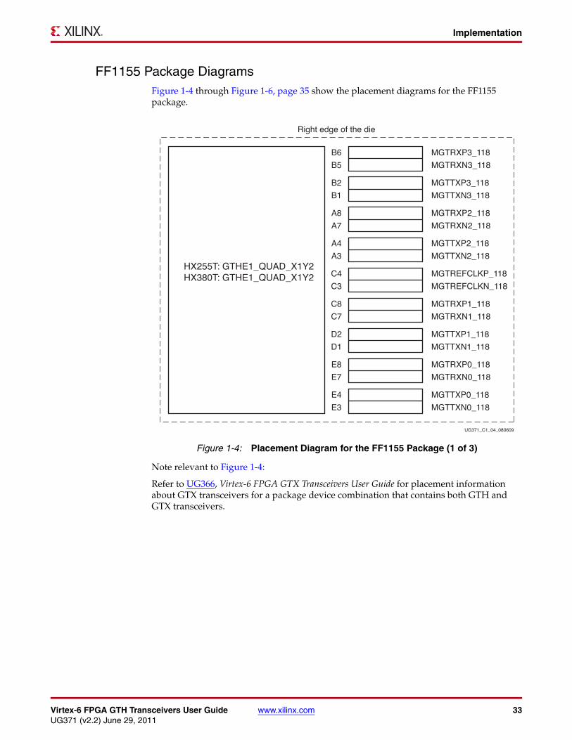
Implementation
FF1155 Package DiagramsFigure 1-4 through Figure 1-6, page 35 show the placement diagrams for the FF1155 package.
Note relevant to Figure 1-4:
Refer to UG366, Virtex-6 FPGA GTX Transceivers User Guide for placement information about GTX transceivers for a package device combination that contains both GTH and GTX transceivers.
X-Ref Target - Figure 1-4
Figure 1-4: Placement Diagram for the FF1155 Package (1 of 3)
HX255T: GTHE1_QUAD_X1Y2HX380T: GTHE1_QUAD_X1Y2
B6
B5
Right edge of the die
MGTRXP3_118
MGTRXN3_118
B2
B1
MGTTXP3_118
MGTTXN3_118
A8
A7
MGTRXP2_118
MGTRXN2_118
UG371_C1_04_080609
A4
A3
MGTTXP2_118
MGTTXN2_118
C4
C3
MGTREFCLKP_118
MGTREFCLKN_118
C8
C7
MGTRXP1_118
MGTRXN1_118
D2
D1
MGTTXP1_118
MGTTXN1_118
E8
E7
MGTRXP0_118
MGTRXN0_118
E4
E3
MGTTXP0_118
MGTTXN0_118

34 www.xilinx.com Virtex-6 FPGA GTH Transceivers User GuideUG371 (v2.2) June 29, 2011
Chapter 1: Transceiver and Tool Overview
Note relevant to Figure 1-5:
1. Refer to UG366, Virtex-6 FPGA GTX Transceivers User Guide for placement information about GTX transceivers for a package device combination that contains both GTH and GTX transceivers.
X-Ref Target - Figure 1-5
Figure 1-5: Placement Diagram for the FF1155 Package (2 of 3)
HX255T: GTHE1_QUAD_X1Y1HX380T: GTHE1_QUAD_X1Y1
F6
F5
Right edge of the die
MGTRXP3_117
MGTRXN3_117
G4
G3
MGTTXP3_117
MGTTXN3_117
D6
D5
MGTRXP2_117
MGTRXN2_117
UG371_C1_05_080609
F2
F1
MGTTXP2_117
MGTTXN2_117
H2
H1
MGTREFCLKP_117
MGTREFCLKN_117
H6
H5
MGTRXP1_117
MGTRXN1_117
J4
J3
MGTTXP1_117
MGTTXN1_117
K6
K5
MGTRXP0_117
MGTRXN0_117
K2
K1
MGTTXP0_117
MGTTXN0_117

Virtex-6 FPGA GTH Transceivers User Guide www.xilinx.com 35UG371 (v2.2) June 29, 2011
Implementation
Note relevant to Figure 1-6:
1. Refer to UG366, Virtex-6 FPGA GTX Transceivers User Guide for placement information about GTX transceivers for a package device combination that contains both GTH and GTX transceivers.
X-Ref Target - Figure 1-6
Figure 1-6: Placement Diagram for the FF1155 Package (3 of 3)
HX255T: GTHE1_QUAD_X1Y0HX380T: GTHE1_QUAD_X1Y0
M6
M5
Right edge of the die
MGTRXP3_116
MGTRXN3_116
M2
M1
MGTTXP3_116
MGTTXN3_116
N4
N3
MGTRXP2_116
MGTRXN2_116
UG371_C1_06_080609
L4
L3
MGTTXP2_116
MGTTXN2_116
P6
P5
MGTREFCLKP_116
MGTREFCLKN_116
R4
R3
MGTRXP1_116
MGTRXN1_116
P2
P1
MGTTXP1_116
MGTTXN1_116
U4
U3
MGTRXP0_116
MGTRXN0_116
T2
T1
MGTTXP0_116
MGTTXN0_116

36 www.xilinx.com Virtex-6 FPGA GTH Transceivers User GuideUG371 (v2.2) June 29, 2011
Chapter 1: Transceiver and Tool Overview
FF1923 and FF1924 Package DiagramsFigure 1-7 through Figure 1-12, page 41 show the placement diagrams for the FF1923 and FF1924 packages. The XC6VHX255T device is available only in the FF1923 package.
Notes relevant to Figure 1-7:
1. The XC6VHX255T device is available only in the FF1923 package.
2. Refer to UG366, Virtex-6 FPGA GTX Transceivers User Guide for placement information about GTX transceivers for a package device combination that contains both GTH and GTX transceivers.
X-Ref Target - Figure 1-7
Figure 1-7: Placement Diagram for the FF1923 and FF1924 Packages (1 of 6)
HX255T: GTHE1_QUAD_X1Y2HX380T: GTHE1_QUAD_X1Y2HX565T: GTHE1_QUAD_X1Y2
D6
D5
Right edge of the die
MGTRXP3_118
MGTRXN3_118
C4
C3
MGTTXP3_118
MGTTXN3_118
B6
B5
MGTRXP2_118
MGTRXN2_118
UG371_C1_07_080609
A4
A3
MGTTXP2_118
MGTTXN2_118
E4
E3
MGTREFCLKP_118
MGTREFCLKN_118
F6
F5
MGTRXP1_118
MGTRXN1_118
D2
D1
MGTTXP1_118
MGTTXN1_118
G8
G7
MGTRXP0_118
MGTRXN0_118
F2
F1
MGTTXP0_118
MGTTXN0_118
Virtex-6 FPGA GTH Transceivers User Guide www.xilinx.com 37UG371 (v2.2) June 29, 2011
Implementation
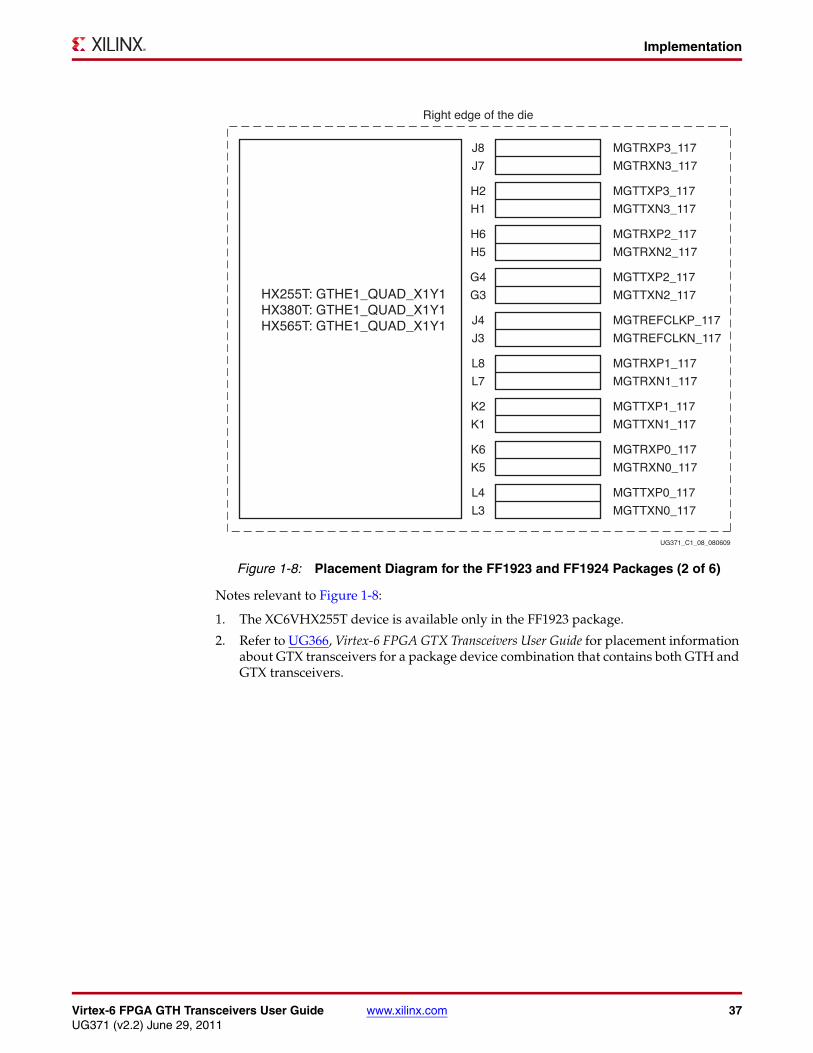
Notes relevant to Figure 1-8:
1. The XC6VHX255T device is available only in the FF1923 package.
2. Refer to UG366, Virtex-6 FPGA GTX Transceivers User Guide for placement information about GTX transceivers for a package device combination that contains both GTH and GTX transceivers.
X-Ref Target - Figure 1-8
Figure 1-8: Placement Diagram for the FF1923 and FF1924 Packages (2 of 6)
HX255T: GTHE1_QUAD_X1Y1HX380T: GTHE1_QUAD_X1Y1HX565T: GTHE1_QUAD_X1Y1
J8
J7
Right edge of the die
MGTRXP3_117
MGTRXN3_117
H2
H1
MGTTXP3_117
MGTTXN3_117
H6
H5
MGTRXP2_117
MGTRXN2_117
UG371_C1_08_080609
G4
G3
MGTTXP2_117
MGTTXN2_117
J4
J3
MGTREFCLKP_117
MGTREFCLKN_117
L8
L7
MGTRXP1_117
MGTRXN1_117
K2
K1
MGTTXP1_117
MGTTXN1_117
K6
K5
MGTRXP0_117
MGTRXN0_117
L4
L3
MGTTXP0_117
MGTTXN0_117

38 www.xilinx.com Virtex-6 FPGA GTH Transceivers User GuideUG371 (v2.2) June 29, 2011
Chapter 1: Transceiver and Tool Overview
Notes relevant to Figure 1-9:
1. The XC6VHX255T device is available only in the FF1923 package.
2. Refer to UG366, Virtex-6 FPGA GTX Transceivers User Guide for placement information about GTX transceivers for a package device combination that contains both GTH and GTX transceivers.
X-Ref Target - Figure 1-9
Figure 1-9: Placement Diagram for the FF1923 and FF1924 Packages (3 of 6)
HX255T: GTHE1_QUAD_X1Y0HX380T: GTHE1_QUAD_X1Y0HX565T: GTHE1_QUAD_X1Y0
M6
M5
Right edge of the die
MGTRXP3_116
MGTRXN3_116
N4
N3
MGTTXP3_116
MGTTXN3_116
N8
N7
MGTRXP2_116
MGTRXN2_116
UG371_C1_09_080609
M2
M1
MGTTXP2_116
MGTTXN2_116
R4
R3
MGTREFCLKP_116
MGTREFCLKN_116
T6
T5
MGTRXP1_116
MGTRXN1_116
P2
P1
MGTTXP1_116
MGTTXN1_116
U4
U3
MGTRXP0_116
MGTRXN0_116
T2
T1
MGTTXP0_116
MGTTXN0_116

Virtex-6 FPGA GTH Transceivers User Guide www.xilinx.com 39UG371 (v2.2) June 29, 2011
Implementation
Notes relevant to Figure 1-10:
1. The XC6VHX255T device is available only in the FF1923 package.
2. Refer to UG366, Virtex-6 FPGA GTX Transceivers User Guide for placement information about GTX transceivers for a package device combination that contains both GTH and GTX transceivers.
X-Ref Target - Figure 1-10
Figure 1-10: Placement Diagram for the FF1923 and FF1924 Packages (4 of 6)
HX255T: GTHE1_QUAD_X0Y2HX380T: GTHE1_QUAD_X0Y2HX565T: GTHE1_QUAD_X0Y2
D39
D40
Left edge of the die
MGTRXP3_108
MGTRXN3_108
C41
C42
MGTTXP3_108
MGTTXN3_108
B39
B40
MGTRXP2_108
MGTRXN2_108
UG371_C1_10_080609
A41
A42
MGTTXP2_108
MGTTXN2_108
E41
E42
MGTREFCLKP_108
MGTREFCLKN_108
F39
F40
MGTRXP1_108
MGTRXN1_108
D43
D44
MGTTXP1_108
MGTTXN1_108
G37
G38
MGTRXP0_108
MGTRXN0_108
F43
F44
MGTTXP0_108
MGTTXN0_108

40 www.xilinx.com Virtex-6 FPGA GTH Transceivers User GuideUG371 (v2.2) June 29, 2011
Chapter 1: Transceiver and Tool Overview
Notes relevant to Figure 1-11:
1. The XC6VHX255T device is available only in the FF1923 package.
2. Refer to UG366, Virtex-6 FPGA GTX Transceivers User Guide for placement information about GTX transceivers for a package device combination that contains both GTH and GTX transceivers.
X-Ref Target - Figure 1-11
Figure 1-11: Placement Diagram for the FF1923 and FF1924 Packages (5 of 6)
HX255T: GTHE1_QUAD_X0Y1HX380T: GTHE1_QUAD_X0Y1HX565T: GTHE1_QUAD_X0Y1
J37
J38
Left edge of the die
MGTRXP3_107
MGTRXN3_107
H43
H44
MGTTXP3_107
MGTTXN3_107
H39
H40
MGTRXP2_107
MGTRXN2_107
UG371_C1_11_080609
G41
G42
MGTTXP2_107
MGTTXN2_107
J41
J42
MGTREFCLKP_107
MGTREFCLKN_107
L37
L38
MGTRXP1_107
MGTRXN1_107
K43
K44
MGTTXP1_107
MGTTXN1_107
K39
K40
MGTRXP0_107
MGTRXN0_107
L41
L42
MGTTXP0_107
MGTTXN0_107
Virtex-6 FPGA GTH Transceivers User Guide www.xilinx.com 41UG371 (v2.2) June 29, 2011
Implementation
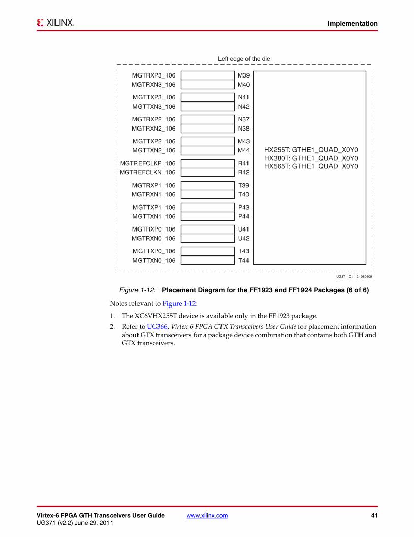
Notes relevant to Figure 1-12:
1. The XC6VHX255T device is available only in the FF1923 package.
2. Refer to UG366, Virtex-6 FPGA GTX Transceivers User Guide for placement information about GTX transceivers for a package device combination that contains both GTH and GTX transceivers.
X-Ref Target - Figure 1-12
Figure 1-12: Placement Diagram for the FF1923 and FF1924 Packages (6 of 6)
HX255T: GTHE1_QUAD_X0Y0HX380T: GTHE1_QUAD_X0Y0HX565T: GTHE1_QUAD_X0Y0
M39
M40
Left edge of the die
MGTRXP3_106
MGTRXN3_106
N41
N42
MGTTXP3_106
MGTTXN3_106
N37
N38
MGTRXP2_106
MGTRXN2_106
UG371_C1_12_080609
M43
M44
MGTTXP2_106
MGTTXN2_106
R41
R42
MGTREFCLKP_106
MGTREFCLKN_106
T39
T40
MGTRXP1_106
MGTRXN1_106
P43
P44
MGTTXP1_106
MGTTXN1_106
U41
U42
MGTRXP0_106
MGTRXN0_106
T43
T44
MGTTXP0_106
MGTTXN0_106
42 www.xilinx.com Virtex-6 FPGA GTH Transceivers User GuideUG371 (v2.2) June 29, 2011
Chapter 1: Transceiver and Tool Overview

Virtex-6 FPGA GTH Transceivers User Guide www.xilinx.com 43UG371 (v2.2) June 29, 2011
Chapter 2
Shared Transceiver Features
Reference Clock Input Structure
Functional DescriptionThe reference clock input structure is illustrated in Figure 2-1. The input is terminated internally with 50 on each leg to 2/3 MGTHAVCCPLL. The reference clock input is instantiated in software with an IBUFDS_GTHE1 primitive. Its location is fixed via LOC constraints in the UCF. Refer to Implementation, page 31 for details.
The output of the IBUFDS_GTHE1 primitive drives the REFCLK input of the GTHE1_QUAD primitive. The ports and attributes controlling each of the IBUFDS_GTHE1 primitives are mapped to the respective GTHE1_QUAD primitive.
X-Ref Target - Figure 2-1
Figure 2-1: Reference Clock Input Structure
UG371_c2_14_120809
MGTREFCLKP
MGTREFCLKN
MGTHAVCCPLL_[L,R]
2/3MGTHAVCCPLL_[L,R]
pll_refclk_term_b
MGTHAVCCRX_[L,R]
Nominal 50Ω
Nominal 50Ω

44 www.xilinx.com Virtex-6 FPGA GTH Transceivers User GuideUG371 (v2.2) June 29, 2011
Chapter 2: Shared Transceiver Features
Ports and AttributesTable 2-1 defines the reference clock input structure ports for the GTHE1_QUAD primitive.
Table 2-2 defines the reference clock input structure ports for the IBUFDS_GTHE1 software primitive.
Table 2-3 defines the reference clock input structure attribute for the GTHE1_QUAD software primitive.
Using the Reference ClockThe reference clock is always used in an AC-coupled mode. The recommended value for the AC-coupling capacitors is 100 nF. The LVPECL clock must be used to drive the reference clock pins. Refer to DS152, Virtex-6 FPGA Data Sheet: DC and Switching Characteristics for electrical and switching specifications.
Table 2-1: Reference Clock Input Structure Ports for the GTHE1_QUAD Primitive
Port Dir Clock Domain Description
REFCLK In N/A REFCLK is an external clock driven by the O port of the IBUFDS_GTHE1 software primitive as the reference clock to the GTHE1_QUAD primitive.
Table 2-2: Reference Clock Input Structure Ports for the IBUFDS_GTHE1 Primitive
Port Dir Clock Domain Description
I In Async This port is the positive input of the reference clock differential pair.
IB In Async This port is the negative input of the reference clock differential pair.
O Out Async This port is the output of the reference clock buffer connected to the REFCLK port of the GTHE1_QUAD primitive.
Table 2-3: Reference Clock Input Structure Attribute
Attribute Type Description
PLL_CFG1 16-bit Binary This attribute defaults to 16'h81C0.
[15]: REFCLK termination control (pll_refclk_term_b)
AC-coupled mode: 1'b1
Reserved: 1'b0
[14:0]: Reserved
Reserved: 15'h01C0

Virtex-6 FPGA GTH Transceivers User Guide www.xilinx.com 45UG371 (v2.2) June 29, 2011
Reference Clock Distribution and Selection
Reference Clock Distribution and Selection
Functional DescriptionFor proper high-speed operation, the GTH transceiver requires a high-quality, low-jitter reference clock. Because of the shared PMA PLL architecture inside the GTH Quad, each reference clock sources all four lanes. The reference clock is used to produce the PLL clock, which is divided by one or four to make individual TX and RX serial clocks and parallel clocks for each GTH transceiver.
The GTH Quad reference clock is provided through the REFCLK port. There are two ways to drive the REFCLK port:
• Using an external oscillator to drive GTH dedicated clock routing
• Using a clock from a neighboring GTH Quad through GTH dedicated clock routing (not recommended for GTH transceivers operating a line rates 2.8 Gb/s and above)
Using the dedicated clock routing provides the best possible clock to the GTH Quad. Each GTH Quad has a dedicated clock pin, represented by the IBUFDS_GTHE1 primitive, that can be used to drive the dedicated clock routing.
This clocking section shows how to select the dedicated clocks for use by one or more GTH Quads.
Ports and AttributesTable 2-4 defines the reference clock selection ports..
Table 2-4: Reference Clock Selection Ports
Port Dir Clock Domain Description
PLLREFCLKSEL[2:0] In DCLK Reserved. Tie these inputs to 000.
REFCLK In N/A This input is the external jitter stable clock driven by the IBUFDS_GTHE1 primitive as the reference clock to the GTHE1_QUAD primitive.
TSTREFCLKFAB Out N/A This port provides direct access to the reference clock provided to the shared PLL in the GTHE1_QUAD primitive. The clock is routed through interconnect and can be used to clock FPGA logic.
TSTREFCLKOUT Out N/A This port provides direct access to the reference clock provided to the shared PLL in the GTHE1_QUAD primitive. The clock is routed through the global clock tree (must be connected through a BUFG) and can be used to clock FPGA logic. This port can also connect directly to an MMCM or BUFR.

46 www.xilinx.com Virtex-6 FPGA GTH Transceivers User GuideUG371 (v2.2) June 29, 2011
Chapter 2: Shared Transceiver Features
Table 2-5 defines the reference clock selection attributes..
Clocking from an External SourceEach GTH Quad has a dedicated pin that can be connected to an external clock source. To use these pins, an IBUFDS_GTHE1 primitive is instantiated. In the user constraints file (UCF), the IBUFDS_GTHE1 input pins are constrained to the locations of the dedicated clock pins for the GTH Quad. In the design, the output of the IBUFDS_GTHE1 primitive is connected to the REFCLK input port. The locations of the dedicated pins for all GTH Quads are documented in Implementation, page 31.
Figure 2-2 shows a differential GTH clock pin pair sourced by an external oscillator on the board.
Clocking from a Neighboring GTH QuadThe external reference clock from one GTH Quad can be used to drive the REFCLK input port of the neighboring GTH Quad. The example in Figure 2-3 uses the clock from one GTH Quad to clock one neighbor above and one neighbor below. A GTH Quad shares its clock with its neighbors using the dedicated clock routing resources.
Table 2-5: Reference Clock Selection Attributes
Attribute Type Description
PLL_CFG2 16-bit Hex Reserved. Use the recommended values from the Virtex®-6 FPGA GTH Transceiver Wizard.
X-Ref Target - Figure 2-2
Figure 2-2: Single GTHE1_QUAD Clocked Externally
I
IBREFCLK
MGTREFCLKP
MGTREFCLKN
GTHE1_QUAD
O
UG371_c2_01_082609

Virtex-6 FPGA GTH Transceivers User Guide www.xilinx.com 47UG371 (v2.2) June 29, 2011
Reference Clock Distribution and Selection
These rules must be observed when sharing a reference clock to ensure that jitter margins for high-speed designs are met:
1. The sharing of a reference clock is allowed only for 2.8 Gb/s and below.
2. The external reference clock that drives the REFCLK input port of a given quad (the sourcing GTH Quad) needs to be used by the PLL in the same Quad due to the position of the REFCLK multiplexer.
3. The number of GTH Quads above the sourcing GTH Quad must not exceed one.
4. The number of GTH Quads below the sourcing GTH Quad must not exceed one.
5. The reference clock cannot be routed across the FPGA to the other GTH Quad column.
6. The reference clock cannot be shared with a neighboring GTX transceiver.
The maximum number of GTH transceivers that can be sourced by a single clock pin pair is 12.
X-Ref Target - Figure 2-3
Figure 2-3: Multiple GTHE1_QUADs with Shared Reference Clock
I
IB
REFCLK PLL
OFF
Tied Off Float
Tied Off Float
MGTREFCLKP
MGTREFCLKN
GTHE1_QUAD
O
UG371_c2_02_082609
0
REFCLK PLL
OFF
GTHE1_QUAD
0
REFCLK PLL
OFF
GTHE1_QUAD
0
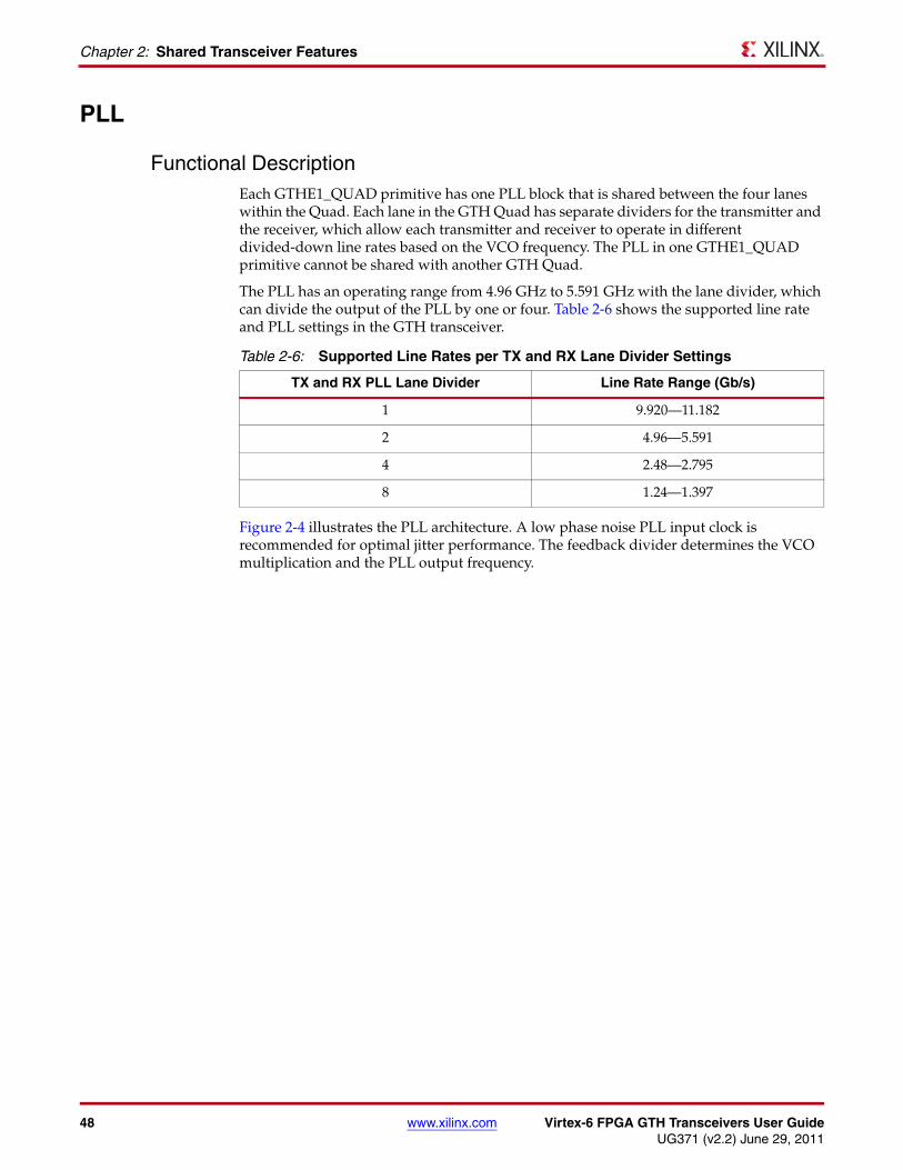
48 www.xilinx.com Virtex-6 FPGA GTH Transceivers User GuideUG371 (v2.2) June 29, 2011
Chapter 2: Shared Transceiver Features
PLL
Functional DescriptionEach GTHE1_QUAD primitive has one PLL block that is shared between the four lanes within the Quad. Each lane in the GTH Quad has separate dividers for the transmitter and the receiver, which allow each transmitter and receiver to operate in different divided-down line rates based on the VCO frequency. The PLL in one GTHE1_QUAD primitive cannot be shared with another GTH Quad.
The PLL has an operating range from 4.96 GHz to 5.591 GHz with the lane divider, which can divide the output of the PLL by one or four. Table 2-6 shows the supported line rate and PLL settings in the GTH transceiver.
Figure 2-4 illustrates the PLL architecture. A low phase noise PLL input clock is recommended for optimal jitter performance. The feedback divider determines the VCO multiplication and the PLL output frequency.
Table 2-6: Supported Line Rates per TX and RX Lane Divider Settings
TX and RX PLL Lane Divider Line Rate Range (Gb/s)
1 9.920—11.182
2 4.96—5.591
4 2.48—2.795
8 1.24—1.397
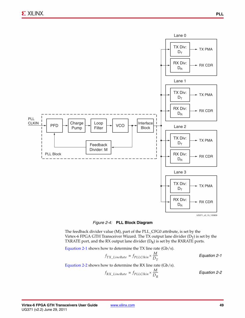
Virtex-6 FPGA GTH Transceivers User Guide www.xilinx.com 49UG371 (v2.2) June 29, 2011
PLL
The feedback divider value (M), part of the PLL_CFG0 attribute, is set by the Virtex-6 FPGA GTH Transceiver Wizard. The TX output lane divider (DT) is set by the TXRATE port, and the RX output lane divider (DR) is set by the RXRATE ports.
Equation 2-1 shows how to determine the TX line rate (Gb/s).
Equation 2-1
Equation 2-2 shows how to determine the RX line rate (Gb/s).
Equation 2-2
X-Ref Target - Figure 2-4
Figure 2-4: PLL Block Diagram
UG371_c2_15_120809
TX PMA
Lane 0
TX Div:DT
RX CDRRX Div:
DR
TX PMA
Lane 1
TX Div:DT
RX CDR
PLLCLKIN
PLL Block
RX Div:DR
PFD VCOChargePump
LoopFilter
FeedbackDivider: M
InterfaceBlock
TX PMA
Lane 2
TX Div:DT
RX CDRRX Div:
DR
TX PMA
Lane 3
TX Div:DT
RX CDRRX Div:
DR
fTX_LineRate fPLLClkinMDT-------=
fRX_LineRate fPLLClkinMDR--------=
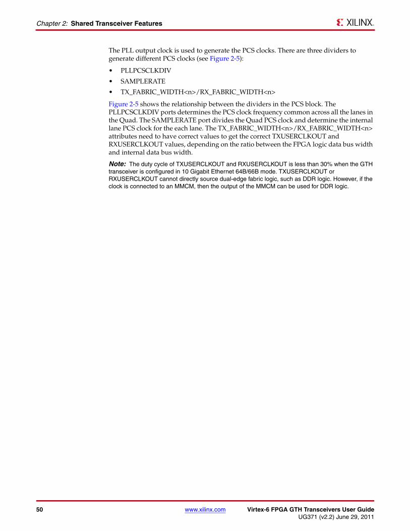
50 www.xilinx.com Virtex-6 FPGA GTH Transceivers User GuideUG371 (v2.2) June 29, 2011
Chapter 2: Shared Transceiver Features
The PLL output clock is used to generate the PCS clocks. There are three dividers to generate different PCS clocks (see Figure 2-5):
• PLLPCSCLKDIV
• SAMPLERATE
• TX_FABRIC_WIDTH<n>/RX_FABRIC_WIDTH<n>
Figure 2-5 shows the relationship between the dividers in the PCS block. The PLLPCSCLKDIV ports determines the PCS clock frequency common across all the lanes in the Quad. The SAMPLERATE port divides the Quad PCS clock and determine the internal lane PCS clock for the each lane. The TX_FABRIC_WIDTH<n>/RX_FABRIC_WIDTH<n> attributes need to have correct values to get the correct TXUSERCLKOUT and RXUSERCLKOUT values, depending on the ratio between the FPGA logic data bus width and internal data bus width.
Note: The duty cycle of TXUSERCLKOUT and RXUSERCLKOUT is less than 30% when the GTH transceiver is configured in 10 Gigabit Ethernet 64B/66B mode. TXUSERCLKOUT or RXUSERCLKOUT cannot directly source dual-edge fabric logic, such as DDR logic. However, if the clock is connected to an MMCM, then the output of the MMCM can be used for DDR logic.

Virtex-6 FPGA GTH Transceivers User Guide www.xilinx.com 51UG371 (v2.2) June 29, 2011
PLL
X-Ref Target - Figure 2-5
Figure 2-5: TX and RX Parallel Clock Dividers in the PCS Block
UG371_c2_16_020210
RX_FABRIC_WIDTH0
TX_FABRIC_WIDTH0SAMPLERATE0[2:0]
RX PCS Clock for Lane 0
TXUSERCLK0
TX PCSClock forLane 0
QuadTX
PCSClock
RXUSERCLK0RECCLK0
Lane 0
TX Lane PCSClock Divider
QUADPLL
PMA Block
Common TXPCS ClockDivider forGTH Quad
RX PCS ClockDivider 0
TX FabricClock Divider
PLLPCSCLKDIV[5:0]
SIPO_Data_Width0
RX FabricClock Divider
RX_FABRIC_WIDTH1
TX_FABRIC_WIDTH1SAMPLERATE1[2:0]
RX PCS Clock for Lane 1
TXUSERCLK1
TX PCSClock forLane 1
RXUSERCLK1
Lane 1
TX Lane PCSClock Divider
TX FabricClock Divider
RX FabricClock Divider
RX_FABRIC_WIDTH2
TX_FABRIC_WIDTH2SAMPLERATE2[2:0]
RX PCS Clock for Lane 2
TXUSERCLK2
TX PCSClock forLane 2
RXUSERCLK2
Lane 2
TX Lane PCSClock Divider
TX FabricClock Divider
RX FabricClock Divider
RX_FABRIC_WIDTH3
TX_FABRIC_WIDTH3SAMPLERATE3[2:0]
RX PCS Clock for Lane 3
TXUSERCLK3
TX PCSClock forLane 3
RXUSERCLK3
Lane 3
TX Lane PCSClock Divider
TX FabricClock Divider
RX FabricClock Divider
CDR0
RECCLK1 RX PCS ClockDivider 1
SIPO_Data_Width1
CDR1
RECCLK2 RX PCS ClockDivider 2
SIPO_Data_Width2
CDR2
RECCLK3 RX PCS ClockDivider 3
SIPO_Data_Width3
CDR3
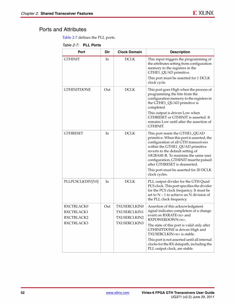
52 www.xilinx.com Virtex-6 FPGA GTH Transceivers User GuideUG371 (v2.2) June 29, 2011
Chapter 2: Shared Transceiver Features
Ports and AttributesTable 2-7 defines the PLL ports.
Table 2-7: PLL Ports
Port Dir Clock Domain Description
GTHINIT In DCLK This input triggers the programming of the attributes setting from configuration memory to the registers in the GTHE1_QUAD primitive.
This port must be asserted for 1 DCLK clock cycle.
GTHINITDONE Out DCLK This port goes High when the process of programming the bits from the configuration memory to the registers in the GTHE1_QUAD primitive is completed.
This output is driven Low when GTHRESET or GTHINIT is asserted. It remains Low until after the assertion of GTHINIT.
GTHRESET In DCLK This port resets the GTHE1_QUAD primitive. When this port is asserted, the configuration of all GTH transceivers within the GTHE1_QUAD primitive reverts to the default setting of 10GBASE-R. To maintain the same user configuration, GTHINIT must be pulsed after GTHRESET is deasserted.
This port must be asserted for 20 DCLK clock cycles.
PLLPCSCLKDIV[5:0] In DCLK PLL output divider for the GTH Quad PCS clock. This port specifies the divider for the PCS clock frequency. It must be set to N – 1 to achieve an N division of the PLL clock frequency.
RXCTRLACK0
RXCTRLACK1
RXCTRLACK2
RXCTRLACK3
Out TXUSERCLKIN0
TXUSERCLKIN1
TXUSERCLKIN2
TXUSERCLKIN3
Assertion of this acknowledgment signal indicates completion of a change event on RXRATE<n> and RXPOWERDOWN<n>.
The state of this port is valid only after GTHINITDONE is driven High and TXUSERCLKIN<n> is stable.
This port is not asserted until all internal clocks for the RX datapath, including the PLL output clock, are stable.
Virtex-6 FPGA GTH Transceivers User Guide www.xilinx.com 53UG371 (v2.2) June 29, 2011
PLL
RXRATE0[1:0]
RXRATE1[1:0]
RXRATE2[1:0]
RXRATE3[1:0]
In TXUSERCLKIN0
TXUSERCLKIN1
TXUSERCLKIN2
TXUSERCLKIN3
This control signal specifies the receiver lane divider values:
00: Full data rate
01: 1/2 data rate
10: 1/4 data rate
11: 1/8 data rate
This port is active after the TX side becomes active. TXUSERCLKIN<n> must be stable to use this port.
This port must always be set to 2'b00 during initialization and when GTHRESET is asserted.
SAMPLERATE0[2:0]
SAMPLERATE1[2:0]
SAMPLERATE2[2:0]
SAMPLERATE3[2:0]
In TXUSERCLKIN0
TXUSERCLKIN1
TXUSERCLKIN2
TXUSERCLKIN3
This control signal specifies the frequency of the strobe signal relative to the internal transmitter PCS clock after the transmitter lane dividers:
Strobe frequency:
PCS clock frequency =
1:1 – SAMPLERATE = 3'b000
1:2 – SAMPLERATE = 3'b001
1:4 – SAMPLERATE = 3'b010
1:8 – SAMPLERATE = 3'b011
This port must always be set to 3'b000 during initialization and when GTHRESET is asserted.
TXCTRLACK0
TXCTRLACK1
TXCTRLACK2
TXCTRLACK3
Out TXUSERCLKIN0
TXUSERCLKIN1
TXUSERCLKIN2
TXUSERCLKIN3
Assertion of this acknowledgment signal indicates completion of a change event on TXRATE<n>, SAMPLERATE<n>, and TXPOWERDOWN<n>.
The state of this port is valid only after GTHINITDONE is driven High and TXUSERCLKIN<n> is stable.
This port is not asserted until all internal clocks for the TX datapath, including the PLL output clock, are stable.
TXRATE0[1:0]
TXRATE1[1:0]
TXRATE2[1:0]
TXRATE3[1:0]
In TXUSERCLKIN0
TXUSERCLKIN1
TXUSERCLKIN2
TXUSERCLKIN3
This control signal specifies the transmitter lane divider values:
00: Full data rate
01: 1/2 data rate
10: 1/4 data rate
11: 1/8 data rate
This port must always be set to 2'b00 during initialization and when GTHRESET is asserted.
Table 2-7: PLL Ports (Cont’d)
Port Dir Clock Domain Description

54 www.xilinx.com Virtex-6 FPGA GTH Transceivers User GuideUG371 (v2.2) June 29, 2011
Chapter 2: Shared Transceiver Features
Table 2-8 defines supported PLLPCSCLKDIV and SAMPLERATE<n> settings in 1/2, 1/4, 1/8 line rates for both raw mode and 8B/10B mode.
Table 2-9 defines the PLL attributes.
Table 2-8: PLLPCSCLKDIV and SAMPLERATE<n> Settings for Divided Line Rate Modes
Mode TX_FABRIC_WIDTH<n> TX/RXRATE<n> SAMPLERATE<n> PLLPCSCLKDIV (1)
1/2 rate 16 2'b01 3'b000 6'h0F
1/4 rate 16 2'b10 3'b000 6'h1F
1/8 rate 16 2'b11 3'b001 6'h1F
1/2 rate 20 2'b01 3'b000 6'h13
1/4 rate 20 2'b10 3'b000 6'h27
1/8 rate 20 2'b11 3'b001 6'h27
1. PLLPCSCLKDIV is a GTH Quad level setting; It is applicable to all four lanes.
Table 2-9: PLL Attributes
Attribute Type Description
DLL_CFG0 16-bit Hex Reserved. Use the recommended values from the Virtex-6 FPGA GTH Transceiver Wizard.
DLL_CFG1 16-bit Hex Reserved. Use the recommended values from the Virtex-6 FPGA GTH Transceiver Wizard.
PLL_CFG0 16-bit Hex Reserved.
[15:6]: Tie to 10'b1001111111
[5:0]: PLL feedback divider
PLL_CFG1 16-bit Hex Reserved.
Tie to 16'h81C0
PLL_CFG2 16-bit Hex Reserved. Use the recommended values from the Virtex-6 FPGA GTH Transceiver Wizard.
RX_FABRIC_WIDTH0
RX_FABRIC_WIDTH1
RX_FABRIC_WIDTH2
RX_FABRIC_WIDTH3
Integer This attribute sets the mapping of the internal data width (PCS) to the external data width (fabric) for the receiver. Valid settings are:
“16” (DRP value 3'b000): PCS to Fabric 1:1
“20” (DRP value 3'b000): PCS to Fabric 1:1
“32” (DRP value 3'b011): PCS to Fabric 1:2 32 bit
“40” (DRP value 3'b101): PCS to Fabric 1:2 40 bit
“64” (DRP value 3'b010): PCS to Fabric 1:4 64 bit
“80” (DRP value 3'b110): PCS to Fabric 1:4 80 bit
“6466” (DRP value 3'b111): 64B/66B mode

Virtex-6 FPGA GTH Transceivers User Guide www.xilinx.com 55UG371 (v2.2) June 29, 2011
PLL
PLL Settings for the Common ProtocolTable 2-10 shows example PLL divider settings for several standard protocols that the GTH transceiver supports.
TX_FABRIC_WIDTH0
TX_FABRIC_WIDTH1
TX_FABRIC_WIDTH2
TX_FABRIC_WIDTH3
Integer This attribute sets the mapping of the internal data width (PCS) to the external data width (fabric) for the transmitter. Valid settings are:
“16” (DRP value 3'b000): PCS to Fabric 1:1
“20” (DRP value 3'b000): PCS to Fabric 1:1
“32” (DRP value 3'b011): PCS to Fabric 1:2 32 bit
“40” (DRP value 3'b101): PCS to Fabric 1:2 40 bit
“64” (DRP value 3'b010): PCS to Fabric 1:4 64 bit
“80” (DRP value 3'b110): PCS to Fabric 1:4 80 bit
“6466” (DRP value 3'b111): 64B/66B mode
Table 2-9: PLL Attributes (Cont’d)
Attribute Type Description
Table 2-10: PLL Divider Settings for Common Protocols
Protocol Line Rate [Gb/s]
REFCLK [MHz]
PLL Feedback Divider
PLL_CFG0[5:0](N – 1)
PLL Freq [GHz]
TXRATERXRATE
PLLPCSCLKDIV(N – 1)
Quad PCS
Clock[MHz]
SAMPLERATE
Lane PCS
Clock
TX_FABRIC_WIDTHRX_FABRIC_WIDTH
(Note 1)
TXUSERCLKRXUSERCLK
10GBASE-KR 10.3125 156.25 32 5.15625 2'b00 32 156.25 3'b000 156.25 3'b111 156.25
CEI11 11.096 173.37 31 5.54784 2'b00 7 693.75 3'b000 693.75 3'b010 173.44
OC-192
9.953 155.52 31 4.9765 2'b00 7 622.06 3'b000 622.06 3'b010 155.52
9.953 311.03 15 4.9765 2'b00 7 622.06 3'b000 622.06 3'b010 155.52
9.953 622.06 7 4.9765 2'b00 7 622.06 3'b000 622.06 3'b010 155.52
OC-48
2.488 155.52 31 4.976 2'b10 31(2) 622.06 3'b000(2) 155.5 3'b000 155.5
2.488 311.03 15 4.976 2'b10 31(2) 622.06 3'b000(2) 155.5 3'b000 155.5
2.488 622.06 7 4.976 2'b10 31(2) 622.06 3'b000(2) 155.5 3'b000 155.5
OTU12.677 166.69 31 5.334 2'b10 31(2) 666.75 3'b000(2) 166.69 3'b000 166.69
2.677 666.75 7 5.334 2'b10 31(2) 666.75 3'b000(2) 166.69 3'b000 166.69
OTU210.709 167.33 31 5.35456 2'b00 7 669.31 3'b000 669.31 3'b010 167.33
10.709 669.31 7 5.35504 2'b00 7 669.31 3'b000 669.31 3'b010 167.33
OTU310.7546 168.05 31 5.3773 2'b00 7 672.16 3'b000 672.16 3'b010 168.04
10.7546 672.19 7 5.3773 2'b00 7 672.16 3'b000 672.16 3'b010 168.04
OTU411.18 174.69 31 5.590 2'b00 7 698.75 3'b000 698.75 3'b010 174.69
11.18 698.75 7 5.590 2'b00 7 698.75 3'b000 698.75 3'b010 174.69
XFP 9.953 155.52 31 4.9765 2'b00 7 622.07 3'b000 622.07 3'b010 155.52
XLAUI 10.3125 156.25 32 5.15625 2'b00 32 156.25 3'b000 156.25 3'b101 257.81
56 www.xilinx.com Virtex-6 FPGA GTH Transceivers User GuideUG371 (v2.2) June 29, 2011
Chapter 2: Shared Transceiver Features
Reset and Initialization
Functional DescriptionThe different ways to reset the GTH Quad are:
1. Power-up and configure the FPGA.
2. Apply a reset sequence to the GTHRESET and GTHINIT ports.
3. Reset the PCS logic using the power-down ports.
All these methods are described in this section.
These items must be considered to initialize the GTH Quad properly:
• DCLK must always be provided to the GTHE1_QUAD primitive even if the DRP or management interface is not used.
Note: DCLK must be sourced from a free-running clock. It cannot be sourced from TSTREFCLKOUT or TSTREFCLKFAB of the GTH Quad.
• Asserting GTHRESET not only resets the GTH Quad but also changes its configuration back to its default of 10GBASE-R. For example, if the design is configured for OC-192, asserting GTHRESET changes the configuration to 10GBASE-R.
• To keep the user configuration after GTHRESET is deasserted, GTHINIT must be pulsed.
• Both TXUSERCLKIN<n> and RXUSERCLKIN<n> clocks must be stable when TXPOWERDOWN<n> and RXPOWERDOWN<n> are set in normal operation mode.
• The PCS_MODE_LANE<n>, PCS_RESET_LANE<n>, and PCS_RESET_1_LANE<n> attributes must be set to the datapath mode configuration used in the application.
CAUI 10.3125 156.25 32 5.15625 2'b00 32 156.25 3'b000 156.25 3'b101 257.81
Notes: 1. The settings for the TX_FABRIC_WIDTH and RX_FABRIC_WIDTH listed in this table are examples. The settings depend on the
external data width that the user selects for the fabric logic.2. The settings of 3'b000 for SAMPLERATE and 31 for PLLPCSCLKDIV are applicable only when TX/RX_FABRIC_WIDTH are set to
3'b000 (or 16). For higher settings of TX/RX_FABRIC_WIDTH, use 3'b010 for SAMPLERATE and 7 for PLLPCSCLKDIV.
Table 2-10: PLL Divider Settings for Common Protocols (Cont’d)
Protocol Line Rate [Gb/s]
REFCLK [MHz]
PLL Feedback Divider
PLL_CFG0[5:0](N – 1)
PLL Freq [GHz]
TXRATERXRATE
PLLPCSCLKDIV(N – 1)
Quad PCS
Clock[MHz]
SAMPLERATE
Lane PCS
Clock
TX_FABRIC_WIDTHRX_FABRIC_WIDTH
(Note 1)
TXUSERCLKRXUSERCLK

Virtex-6 FPGA GTH Transceivers User Guide www.xilinx.com 57UG371 (v2.2) June 29, 2011
Reset and Initialization
Ports and AttributesTable 2-11 defines the reset ports.
Table 2-11: Reset Ports
Port Dir Clock Domain Description
DCLK In N/A This input is the DRP interface clock. It is also used as the management interface clock when the management interface is enabled. This clock must be connected and available all the time for the GTHE1_QUAD primitive to initialize properly, even if the DRP or the management interface is not used in the design.
DISABLE_DRP In DCLK This input switches between the DRP and the management interface blocks.
0: DRP interface is selected.
1: Management interface is selected.
GTHINIT In DCLK This input triggers the programming of the attributes setting from configuration memory to the registers in the GTHE1_QUAD primitive.
This port must be asserted for 1 DCLK clock cycle.
GTHINITDONE Out DCLK This port is driven High upon completion of programming the bits from the configuration memory to the registers in the GTHE1_QUAD primitive.
This output is driven Low when GTHRESET or GTHINIT is asserted. It remains Low until after the assertion of GTHINIT.
GTHRESET In DCLK This port resets the GTHE1_QUAD primitive. When this port is asserted, the configuration of all GTH transceivers within the GTHE1_QUAD primitive reverts to the default setting of 10GBASE-R. To maintain the same user configuration, GTHINIT must be pulsed after GTHRESET is deasserted.
This port must be asserted for 20 DCLK clock cycles.
MGMTPCSLANESEL[3:0] In DCLK These inputs select the GTH lane of the management interface:
0001: Select GTH lane 0.
0010: Select GTH lane 1.
0100: Select GTH lane 2.
1000: Select GTH lane 3.
The user can select more than one GTH lane for accessing the registers.
MGMTPCSMMDADDR[4:0] In DCLK This input bus is the MMD address bus.
MGMTPCSRDACK Out DCLK This output is the management interface read data valid signal.
It indicates when data is valid for read operations.
MGMTPCSRDDATA[15:0] Out DCLK This output bus is the management interface register read data bus.

58 www.xilinx.com Virtex-6 FPGA GTH Transceivers User GuideUG371 (v2.2) June 29, 2011
Chapter 2: Shared Transceiver Features
MGMTPCSREGADDR[15:0] In DCLK This input bus is the management interface register address bus.
MGMTPCSREGRD In DCLK This input is the management interface read request valid signal.
MGMTPCSREGWR In DCLK This input is the management interface write request valid signal.
MGMTPCSWRDATA[15:0] In DCLK This input bus is the management interface register write data bus.
RXBUFRESET0
RXBUFRESET1
RXBUFRESET2
RXBUFRESET3
In RXUSERCLKIN0
RXUSERCLKIN1
RXUSERCLKIN2
RXUSERCLKIN3
This input resets the buffer inside the RX data converter (see Figure 4-5, page 146). Both the internal RX clock and RXUSERCLKIN<n>(1) must be stable before a reset can be applied to the buffer.
RXCTRLACK0
RXCTRLACK1
RXCTRLACK2
RXCTRLACK3
Out TXUSERCLKIN0
TXUSERCLKIN1
TXUSERCLKIN2
TXUSERCLKIN3
Assertion of this acknowledgment signal indicates completion of a change event on RXRATE<n> and RXPOWERDOWN<n>.
The state of this port is valid only after GTHINITDONE is driven High and TXUSERCLKIN<n> is stable.
RXPOWERDOWN0[1:0]
RXPOWERDOWN1[1:0]
RXPOWERDOWN2[1:0]
RXPOWERDOWN3[1:0]
In TXUSERCLKIN0
TXUSERCLKIN1
TXUSERCLKIN2
TXUSERCLKIN3
This control signal requests the receiver power state:
00: Normal operation.
10: Power off receiver logic. The PLL continues to operate in this state.
This port must always be set to 2'b10 during initialization and when GTHRESET is asserted.
If the Quad is configured as a x4 link, only the port from Lane 0 is valid.
RXRATE0[1:0]
RXRATE1[1:0]
RXRATE2[1:0]
RXRATE3[1:0]
In TXUSERCLKIN0
TXUSERCLKIN1
TXUSERCLKIN2
TXUSERCLKIN3
This control signal specifies the receiver lane divider values:
00: Full data rate
01: 1/2 data rate
10: 1/4 data rate
11: 1/8 data rate
This port is active after the TX side becomes active. TXUSERCLKIN<n> must be stable to use this port.
This port must always be set to 2'b00 during initialization and when GTHRESET is asserted.
RXUSERCLKIN0
RXUSERCLKIN1
RXUSERCLKIN2
RXUSERCLKIN3
In N/A This port provides a clock for the internal receiver PCS datapath. It is a buffered version of RXUSERCLKOUT<n>.
Table 2-11: Reset Ports (Cont’d)
Port Dir Clock Domain Description

Virtex-6 FPGA GTH Transceivers User Guide www.xilinx.com 59UG371 (v2.2) June 29, 2011
Reset and Initialization
SAMPLERATE0[2:0]
SAMPLERATE1[2:0]
SAMPLERATE2[2:0]
SAMPLERATE3[2:0]
In TXUSERCLKIN0
TXUSERCLKIN1
TXUSERCLKIN2
TXUSERCLKIN3
This control signal specifies the frequency of the strobe signal relative to the internal transmitter PCS clock after the transmitter lane dividers:
Strobe frequency:
PCS clock frequency =
1:1 – SAMPLERATE = 3'b000
1:2 – SAMPLERATE = 3'b001
1:4 – SAMPLERATE = 3'b010
1:8 – SAMPLERATE = 3'b011
When PCS_MODE_LANE<n>[3:0] = 4'b1010 (16-bit raw) and TX_FABRIC_WIDTH = 16, SAMPLERATE is tied to 3'b000.
Otherwise, SAMPLERATE[2] = 1'b0 and SAMPLERATE[1:0] = TXRATE.
This port must always be set to 3'b000 during initialization and when GTHRESET is asserted.
TXBUFRESET0
TXBUFRESET1
TXBUFRESET2
TXBUFRESET3
In TXUSERCLKIN0
TXUSERCLKIN1
TXUSERCLKIN2
TXUSERCLKIN3
This input resets the buffer inside the TX data converter (see Figure 3-2, page 89). Both the internal TX clock and TXUSERCLKIN<n> must be stable before a reset can be applied to the buffer.
TXCTRLACK0
TXCTRLACK1
TXCTRLACK2
TXCTRLACK3
Out TXUSERCLKIN0
TXUSERCLKIN1
TXUSERCLKIN2
TXUSERCLKIN3
This acknowledgment signal indicates completion of a change event on TXRATE<n>, SAMPLERATE<n>, and TXPOWERDOWN<n>.
The state of this port is valid only after the GTHINITDONE is driven High and TXUSERCLKIN<n> is stable.
TXPOWERDOWN0[1:0]
TXPOWERDOWN1[1:0]
TXPOWERDOWN2[1:0]
TXPOWERDOWN3[1:0]
In TXUSERCLKIN0
TXUSERCLKIN1
TXUSERCLKIN2
TXUSERCLKIN3
This control signal requests the transmitter power state:
00: Normal operation
10: Power off transmitter logic. The PLL continues to operate in this state.
This port must always be set to 2'b10 during initialization and when GTHRESET is asserted.
If the Quad is configured as a x4 link, only the port from Lane 0 is valid.
TXRATE0[1:0]
TXRATE1[1:0]
TXRATE2[1:0]
TXRATE3[1:0]
In TXUSERCLKIN0
TXUSERCLKIN1
TXUSERCLKIN2
TXUSERCLKIN3
This control signal specifies the transmitter lane divider values:
00: Full data rate
01: 1/2 data rate
10: 1/4 data rate
11: 1/8 data rate
This port must always be set to 2'b00 during initialization and when GTHRESET is asserted.
Table 2-11: Reset Ports (Cont’d)
Port Dir Clock Domain Description

60 www.xilinx.com Virtex-6 FPGA GTH Transceivers User GuideUG371 (v2.2) June 29, 2011
Chapter 2: Shared Transceiver Features
TXUSERCLKIN0
TXUSERCLKIN1
TXUSERCLKIN2
TXUSERCLKIN3
In N/A This port provides a clock for the internal transmitter PCS datapath. It is a buffered version of the TXUSERCLKOUT<n>.
This clock must be stable for RXCTRLACK<n> and RXRATE<n> ports to be active.
Notes: 1. <n> denotes lane 0, 1, 2, or 3.
Table 2-11: Reset Ports (Cont’d)
Port Dir Clock Domain Description

Virtex-6 FPGA GTH Transceivers User Guide www.xilinx.com 61UG371 (v2.2) June 29, 2011
Reset and Initialization
Table 2-12 defines the reset attributes.
Table 2-12: Reset Attributes
Attribute Type Description
PCS_MODE_LANE0
PCS_MODE_LANE1
PCS_MODE_LANE2
PCS_MODE_LANE3
16-bit Hex This attribute sets the PCS mode.
[15]: Loopback serializer/deserializer RX to serializer/deserializer TX
[14]: Loopback PCS TX to PCS RX
[13:11]: PRBS generator mode
000: None001: PRBS7010: PRBS9011: PRBS11100: PRBS23101: PRBS31Others: Reserved
[10:8]: PRBS checker mode
000: None001: PRBS7010: PRBS9011: PRBS11100: PRBS23101: PRBS31Others: Reserved
[7:4]: PCS RX mode
0000: Zero0001: 64B/66B0111: 8B/10B1010: 16-bit raw data1011: 20-bit raw data1100: PRBSOthers: Reserved
[3:0]: PCS TX mode
0000: Zero0001: 64B/66B0111: 8B/10B1010: 16-bit raw data1011: 20-bit raw data1100: PRBSOthers: Reserved
62 www.xilinx.com Virtex-6 FPGA GTH Transceivers User GuideUG371 (v2.2) June 29, 2011
Chapter 2: Shared Transceiver Features
PCS_RESET_LANE0
PCS_RESET_LANE1
PCS_RESET_LANE2
PCS_RESET_LANE3
16-bit Hex This attribute controls the datapath resets. These bits vary by mode:
64B/66B: 0xF3FE8B/10B: 0xFC5BRaw: 0xFF3BPRBS: 0xFFCEDefault: 0xFFFF
[15:12]: Reserved[11]: Reset 64B/66B receive[10]: Reset 64B/66B transmit[9]: Reset 8B/10B receive[8]: Reset 8B/10B transmit[7]: Reset RX FIFO[6]: Reset RX Raw FIFO[5]: Reset PRBS checker[4]: Reset PRBS generator[3]: Reserved[2]: Reset 8B/10B TX FIFO[1]: Reset RX loopback FIFO[0]: Reset 64B/66B and PRBS TX FIFO
PCS_RESET_1_LANE0
PCS_RESET_1_LANE1
PCS_RESET_1_LANE2
PCS_RESET_1_LANE3
16-bit Hex [15:2]: Reserved. Use the recommended values from the Virtex-6 FPGA GTH Transceiver Wizard.
[1:0]: These bits control the datapath resets. They vary by mode:
64B/66B: 2'b108B/10B: 2'b00Raw: 2'b00PRBS: 2'b10Default: 2'b11
LANE_PWR_CTRL_LANE0
LANE_PWR_CTRL_LANE1
LANE_PWR_CTRL_LANE2
LANE_PWR_CTRL_LANE3
16-bit Hex
Reserved. Tie to 16'h0400.
RX_CFG1_LANE0
RX_CFG1_LANE1
RX_CFG1_LANE2
RX_CFG1_LANE3
16-bit Hex
Reserved. Tie to 16'h821F.
RX_CFG0_LANE0
RX_CFG0_LANE1
RX_CFG0_LANE2
RX_CFG0_LANE3
16-bit Hex
Reserved. Tie to 16'h0500.
MISC_CFG 16-bit Hex Reserved. Tie to 16'h0008.
TX_CLK_SEL1_LANE0
TX_CLK_SEL1_LANE1
TX_CLK_SEL1_LANE2
TX_CLK_SEL1_LANE3
16-bit Hex
Reserved. Tie to 16'h2121.
Table 2-12: Reset Attributes (Cont’d)
Attribute Type Description
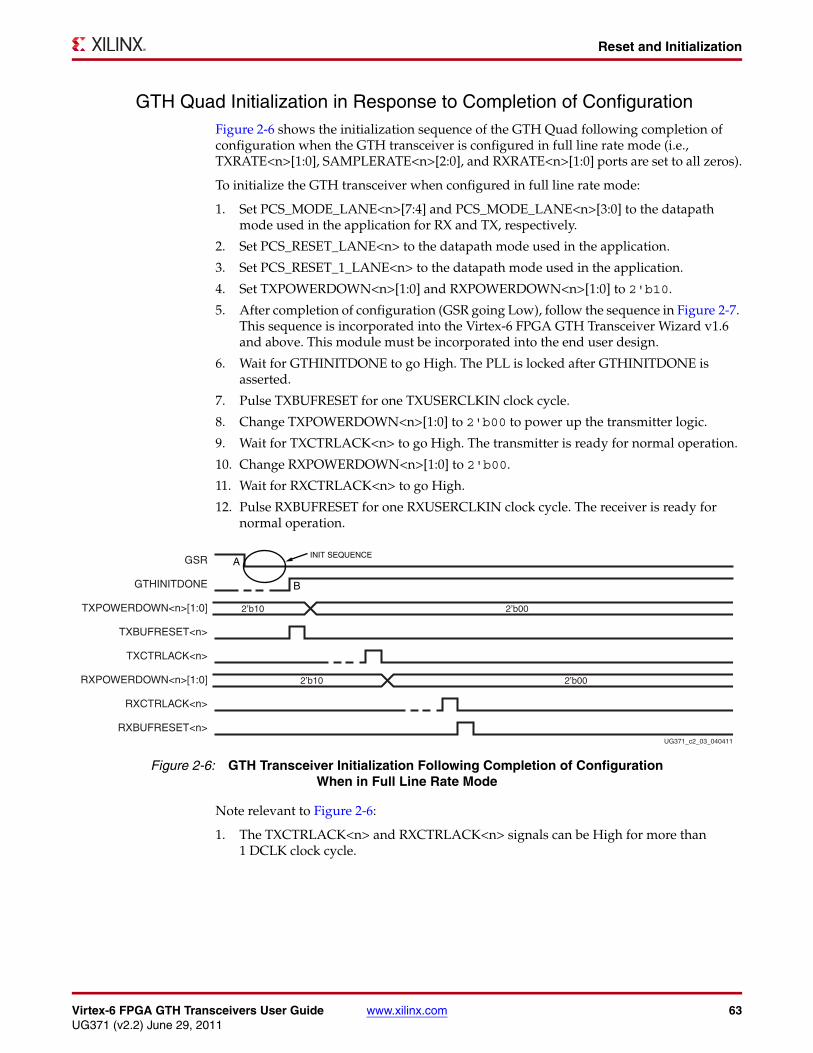
Virtex-6 FPGA GTH Transceivers User Guide www.xilinx.com 63UG371 (v2.2) June 29, 2011
Reset and Initialization
GTH Quad Initialization in Response to Completion of ConfigurationFigure 2-6 shows the initialization sequence of the GTH Quad following completion of configuration when the GTH transceiver is configured in full line rate mode (i.e., TXRATE<n>[1:0], SAMPLERATE<n>[2:0], and RXRATE<n>[1:0] ports are set to all zeros).
To initialize the GTH transceiver when configured in full line rate mode:
1. Set PCS_MODE_LANE<n>[7:4] and PCS_MODE_LANE<n>[3:0] to the datapath mode used in the application for RX and TX, respectively.
2. Set PCS_RESET_LANE<n> to the datapath mode used in the application.
3. Set PCS_RESET_1_LANE<n> to the datapath mode used in the application.
4. Set TXPOWERDOWN<n>[1:0] and RXPOWERDOWN<n>[1:0] to 2'b10.
5. After completion of configuration (GSR going Low), follow the sequence in Figure 2-7. This sequence is incorporated into the Virtex-6 FPGA GTH Transceiver Wizard v1.6 and above. This module must be incorporated into the end user design.
6. Wait for GTHINITDONE to go High. The PLL is locked after GTHINITDONE is asserted.
7. Pulse TXBUFRESET for one TXUSERCLKIN clock cycle.
8. Change TXPOWERDOWN<n>[1:0] to 2'b00 to power up the transmitter logic.
9. Wait for TXCTRLACK<n> to go High. The transmitter is ready for normal operation.
10. Change RXPOWERDOWN<n>[1:0] to 2'b00.
11. Wait for RXCTRLACK<n> to go High.
12. Pulse RXBUFRESET for one RXUSERCLKIN clock cycle. The receiver is ready for normal operation.
Note relevant to Figure 2-6:
1. The TXCTRLACK<n> and RXCTRLACK<n> signals can be High for more than 1 DCLK clock cycle.
X-Ref Target - Figure 2-6
Figure 2-6: GTH Transceiver Initialization Following Completion of ConfigurationWhen in Full Line Rate Mode
GTHINITDONE
GSR
TXPOWERDOWN<n>[1:0]
TXBUFRESET<n>
TXCTRLACK<n>
RXPOWERDOWN<n>[1:0]
RXCTRLACK<n>
RXBUFRESET<n>UG371_c2_03_040411
2’b10 2’b00
2’b10 2’b00
INIT SEQUENCEA
B

64 www.xilinx.com Virtex-6 FPGA GTH Transceivers User GuideUG371 (v2.2) June 29, 2011
Chapter 2: Shared Transceiver Features
Notes relevant to Figure 2-7:
1. 16 MGMT clock cycles assuming 20ns period.Total wait time required is at least 300 ns.
2. Bits [5:0] of MGMT address C000 define the PLL feedback divider of the GTH Quad (set to 31 in this example).
3. MMD address, MGMTPCSMMDADDR[4:0], must be set to 0x01.
Figure 2-8 shows the initialization sequence of the GTH Quad following completion of configuration when the GTH transceiver is configured in divided line rate mode (i.e., TXRATE<n>[1:0], SAMPLERATE<n>[2:0], and RXRATE<n>[1:0] ports are set to non-zero values).
1. Set PCS_MODE_LANE<n>[7:4] and PCS_MODE_LANE<n>[3:0] to the datapath mode used in the application for RX and TX, respectively.
2. Set PCS_RESET_LANE<n> to the datapath mode used in the application.
3. Set PCS_RESET_1_LANE<n> to the datapath mode used in the application.
4. Set TXPOWERDOWN<n>[1:0] and RXPOWERDOWN<n>[1:0] to 2'b10.
5. Set TXRATE<n>[1:0] and RXRATE<n>[1:0] to 2'b00, and set SAMPLERATE<n>[2:0] to 3'b000.
6. After completion of configuration (GSR going Low), follow the initialization sequence in Figure 2-9, page 66. This sequence is incorporated into the Virtex-6 FPGA GTH Transceiver Wizard v1.6 and above. This module must be incorporated into the end-user design.
7. Wait for GTHINITDONE to go High. The PLL is locked after GTHINITDONE is asserted.
8. Change TXRATE<n>[1:0] to the value used for the application and wait for TXCTRLACK to go High.
9. Change SAMPLERATE<n>[2:0] to the value used for the application and wait for TXCTRLACK to go High.
10. Pulse TXBUFRESET for one TXUSERCLKIN clock cycle.
11. Change TXPOWERDOWN<n>[1:0] to 2'b00 to power up the transmitter logic.
X-Ref Target - Figure 2-7
Figure 2-7: GTH Transceiver Initialization Following Completion of Configuration(from A to B in Figure 2-6)
GTHRESET
DISABLE_DRP
MGMTPCSREGADDR[15:0]
GSR
GTHINITDONE
GTHINIT
20
32
2
UG371_c2_18_040411
0008000C 81C0 DFDF2 9FDF2
C003 C001 C000C002
161
MGMTPCSWRDATA[15:0]
2
A
B
8202
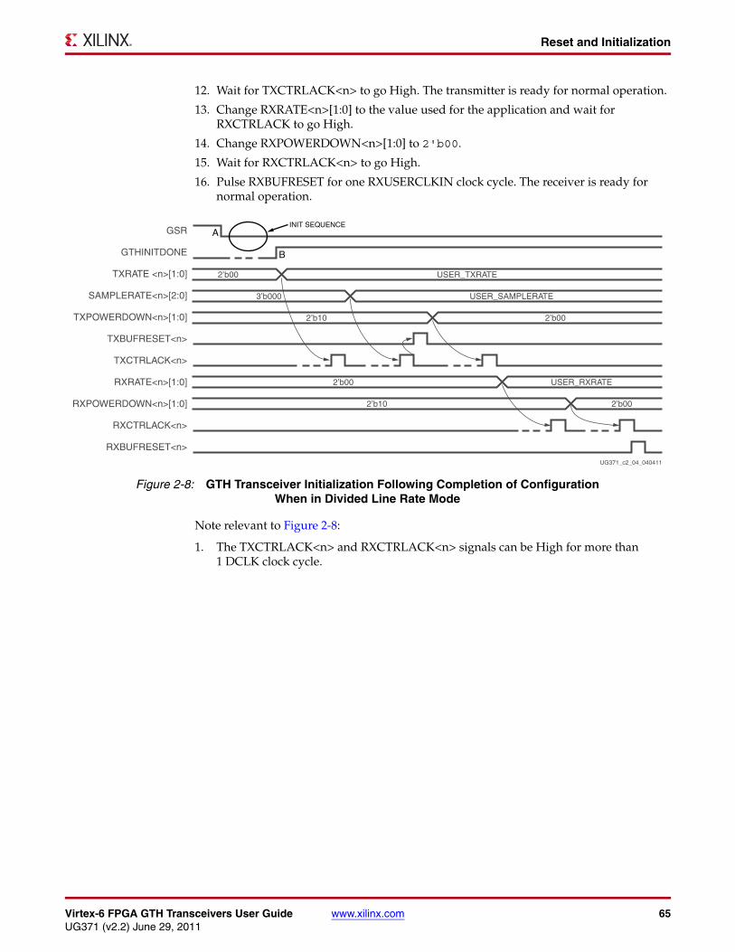
Virtex-6 FPGA GTH Transceivers User Guide www.xilinx.com 65UG371 (v2.2) June 29, 2011
Reset and Initialization
12. Wait for TXCTRLACK<n> to go High. The transmitter is ready for normal operation.
13. Change RXRATE<n>[1:0] to the value used for the application and wait for RXCTRLACK to go High.
14. Change RXPOWERDOWN<n>[1:0] to 2'b00.
15. Wait for RXCTRLACK<n> to go High.
16. Pulse RXBUFRESET for one RXUSERCLKIN clock cycle. The receiver is ready for normal operation.
Note relevant to Figure 2-8:
1. The TXCTRLACK<n> and RXCTRLACK<n> signals can be High for more than 1 DCLK clock cycle.
X-Ref Target - Figure 2-8
Figure 2-8: GTH Transceiver Initialization Following Completion of ConfigurationWhen in Divided Line Rate Mode
GTHINITDONE
GSR
TXRATE <n>[1:0]
SAMPLERATE<n>[2:0]
TXPOWERDOWN<n>[1:0]
TXBUFRESET<n>
TXCTRLACK<n>
RXCTRLACK<n>
RXRATE<n>[1:0]
RXPOWERDOWN<n>[1:0]
RXBUFRESET<n>
UG371_c2_04_040411
2’b00 USER_TXRATE
3’b000 USER_SAMPLERATE
2’b10 2’b00
2’b00 USER_RXRATE
2’b10 2’b00
INIT SEQUENCEA
B

66 www.xilinx.com Virtex-6 FPGA GTH Transceivers User GuideUG371 (v2.2) June 29, 2011
Chapter 2: Shared Transceiver Features
Notes relevant to Figure 2-9:
1. 16 MGMT clock cycles assuming 20ns period.Total wait time required is at least 300ns.
2. Bits [5:0] of MGMT address C000 define the PLL feedback divider of the GTH Quad (set to 31 in this example).
3. MMD address, MGMTPCSMMDADDR[4:0], must be set to 0x01
GTH Quad Reset in Response to GTHRESETGTHRESET is used as a reset to all four GTH lanes within the Quad, including the PLL. Besides resetting the GTH Quad, GTHRESET also changes the Quad to its default configuration of 10GBASE-R. If the GTH Quad has a different configuration from the default of 10GBASE-R, the design must also assert GTHINIT after GTHRESET is deasserted.
Figure 2-10 shows the reset sequence of the GTH Quad following the assertion of GTHRESET when the GTH transceiver is configured in full line rate mode (i.e., the TXRATE<n>[1:0], SAMPLERATE<n>[2:0], and RXRATE<n>[1:0] ports are set to all zeros).
To reset the GTH transceiver when configured in full line rate mode:
1. Set PCS_MODE_LANE<n>[7:4] and PCS_MODE_LANE<n>[3:0] to the datapath mode used in the application for RX and TX, respectively.
2. Set PCS_RESET_LANE<n> to the datapath mode used in the application.
3. Set PCS_RESET_1_LANE<n> to the datapath mode used in the application.
4. Set TXPOWERDOWN<n>[1:0] and RXPOWERDOWN<n>[1:0] to 2'b10.
5. Assert GTHRESET for 20 DCLK clock cycles.
6. Follow the sequence in Figure 2-11. This sequence is incorporated into the Virtex-6 FPGA GTH Transceiver Wizard v1.6 and above. This module must be incorporated into the end user design.
7. Wait for GTHINITDONE to go High. The PLL is locked after GTHINITDONE is asserted.
X-Ref Target - Figure 2-9
Figure 2-9: GTH Transceiver Initialization Following Completion of Configuration(from A to B in Figure 2-8)
GTHRESET
DISABLE_DRP
MGMTPCSREGADDR[15:0]
GSR
GTHINITDONE
GTHINIT
20
32
2
UG371_c2_19_040411
0008000C 81C0 DFDF2 9FDF2
C003 C001 C000C002
161
MGMTPCSWRDATA[15:0]
2
A
B
8202

Virtex-6 FPGA GTH Transceivers User Guide www.xilinx.com 67UG371 (v2.2) June 29, 2011
Reset and Initialization
8. Pulse TXBUFRESET for one TXUSERCLKIN clock cycle.
9. Change TXPOWERDOWN<n>[1:0] to 2'b00 to power up the transmitter logic.
10. Wait for TXCTRLACK<n> to go High. The transmitter is ready for normal operation.
11. Change RXPOWERDOWN<n>[1:0] to 2'b00.
12. Wait for RXCTRLACK<n> to go High.
13. Pulse RXBUFRESET for one RXUSERCLKIN clock cycle. The receiver is ready for normal operation.
Notes relevant to Figure 2-10:
1. The TXCTRLACK<n> and RXCTRLACK<n> signals at this time refer to all four lanes within the Quad. The user must wait for all four TXCTRLACK<n> and RXCTRLACK<n> signals to be deasserted before asserting GTHINIT.
2. The TXCTRLACK<n> and RXCTRLACK<n> signals can be High for more than 1 DCLK clock cycle.
X-Ref Target - Figure 2-10
Figure 2-10: GTH Transceiver Reset Following the Assertion of GTHRESET When in Full Line Rate Mode
GTHINITDONE
GTHINIT
GTHRESET
TXPOWERDOWN<n>[1:0]
TXBUFRESET<n>
TXCTRLACK<n>
RXPOWERDOWN<n>[1:0]
RXCTRLACK<n>
RXBUFRESET<n>
UG371_c2_05_040411
2’b10 2’b00
2’b10
(1)
(1)
2’b00
INIT SEQUENCEA
B
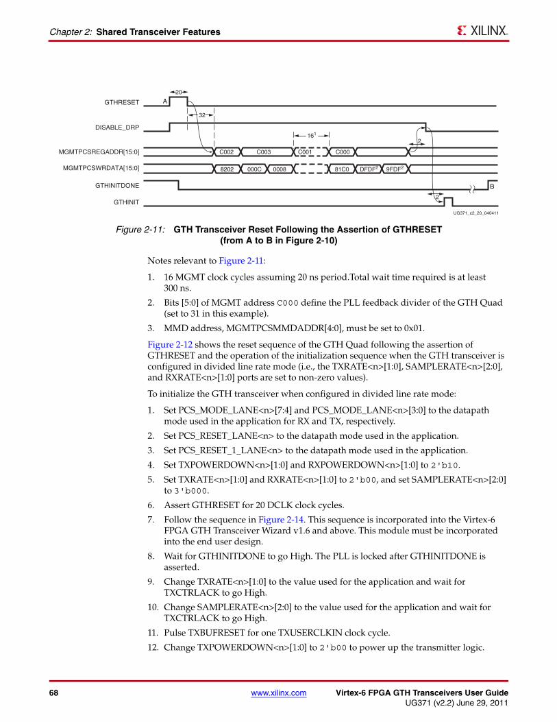
68 www.xilinx.com Virtex-6 FPGA GTH Transceivers User GuideUG371 (v2.2) June 29, 2011
Chapter 2: Shared Transceiver Features
Notes relevant to Figure 2-11:
1. 16 MGMT clock cycles assuming 20 ns period.Total wait time required is at least 300 ns.
2. Bits [5:0] of MGMT address C000 define the PLL feedback divider of the GTH Quad (set to 31 in this example).
3. MMD address, MGMTPCSMMDADDR[4:0], must be set to 0x01.
Figure 2-12 shows the reset sequence of the GTH Quad following the assertion of GTHRESET and the operation of the initialization sequence when the GTH transceiver is configured in divided line rate mode (i.e., the TXRATE<n>[1:0], SAMPLERATE<n>[2:0], and RXRATE<n>[1:0] ports are set to non-zero values).
To initialize the GTH transceiver when configured in divided line rate mode:
1. Set PCS_MODE_LANE<n>[7:4] and PCS_MODE_LANE<n>[3:0] to the datapath mode used in the application for RX and TX, respectively.
2. Set PCS_RESET_LANE<n> to the datapath mode used in the application.
3. Set PCS_RESET_1_LANE<n> to the datapath mode used in the application.
4. Set TXPOWERDOWN<n>[1:0] and RXPOWERDOWN<n>[1:0] to 2'b10.
5. Set TXRATE<n>[1:0] and RXRATE<n>[1:0] to 2'b00, and set SAMPLERATE<n>[2:0] to 3'b000.
6. Assert GTHRESET for 20 DCLK clock cycles.
7. Follow the sequence in Figure 2-14. This sequence is incorporated into the Virtex-6 FPGA GTH Transceiver Wizard v1.6 and above. This module must be incorporated into the end user design.
8. Wait for GTHINITDONE to go High. The PLL is locked after GTHINITDONE is asserted.
9. Change TXRATE<n>[1:0] to the value used for the application and wait for TXCTRLACK to go High.
10. Change SAMPLERATE<n>[2:0] to the value used for the application and wait for TXCTRLACK to go High.
11. Pulse TXBUFRESET for one TXUSERCLKIN clock cycle.
12. Change TXPOWERDOWN<n>[1:0] to 2'b00 to power up the transmitter logic.
X-Ref Target - Figure 2-11
Figure 2-11: GTH Transceiver Reset Following the Assertion of GTHRESET(from A to B in Figure 2-10)
GTHRESET
DISABLE_DRP
MGMTPCSREGADDR[15:0]
GTHINITDONE
GTHINIT
20
32
2
UG371_c2_20_040411
0008000C 81C0 DFDF2 9FDF2
C003 C001 C000C002
161
MGMTPCSWRDATA[15:0]
2
A
8202
B
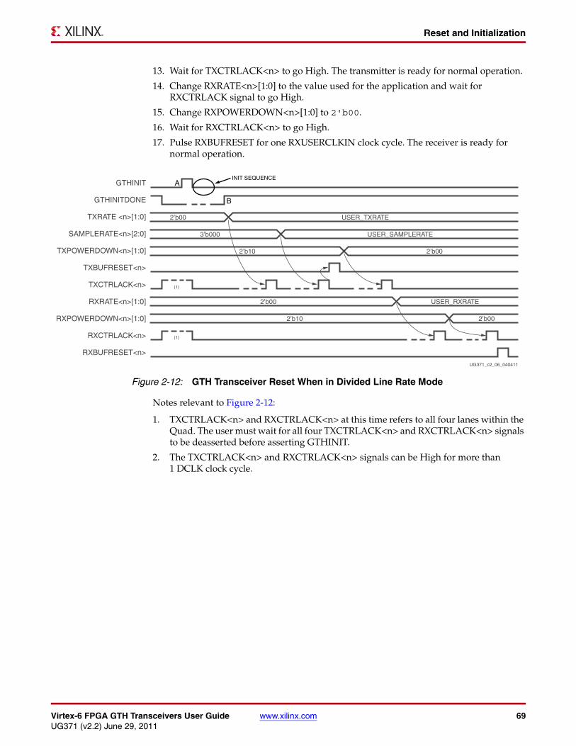
Virtex-6 FPGA GTH Transceivers User Guide www.xilinx.com 69UG371 (v2.2) June 29, 2011
Reset and Initialization
13. Wait for TXCTRLACK<n> to go High. The transmitter is ready for normal operation.
14. Change RXRATE<n>[1:0] to the value used for the application and wait for RXCTRLACK signal to go High.
15. Change RXPOWERDOWN<n>[1:0] to 2'b00.
16. Wait for RXCTRLACK<n> to go High.
17. Pulse RXBUFRESET for one RXUSERCLKIN clock cycle. The receiver is ready for normal operation.
Notes relevant to Figure 2-12:
1. TXCTRLACK<n> and RXCTRLACK<n> at this time refers to all four lanes within the Quad. The user must wait for all four TXCTRLACK<n> and RXCTRLACK<n> signals to be deasserted before asserting GTHINIT.
2. The TXCTRLACK<n> and RXCTRLACK<n> signals can be High for more than 1 DCLK clock cycle.
X-Ref Target - Figure 2-12
Figure 2-12: GTH Transceiver Reset When in Divided Line Rate Mode
GTHINITDONE
GTHINIT
TXRATE <n>[1:0]
SAMPLERATE<n>[2:0]
TXPOWERDOWN<n>[1:0]
TXBUFRESET<n>
TXCTRLACK<n>
RXCTRLACK<n>
RXRATE<n>[1:0]
RXPOWERDOWN<n>[1:0]
RXBUFRESET<n>
UG371_c2_06_040411
2’b00 USER_TXRATE
3’b000 USER_SAMPLERATE
2’b10 2’b00
2’b00 USER_RXRATE
2’b10 2’b00
(1)
(1)
A
B
INIT SEQUENCE

70 www.xilinx.com Virtex-6 FPGA GTH Transceivers User GuideUG371 (v2.2) June 29, 2011
Chapter 2: Shared Transceiver Features
Notes relevant to Figure 2-13:
1. 16 MGMT clock cycles assuming 20 ns period.Total wait time required is at least 300 ns.
2. Bits [5:0] of MGMT address C000 define the PLL feedback divider of the GTH Quad (set to 31 in this example).
3. MMD address, MGMTPCSMMDADDR[4:0], must be set to 0x01.
Resetting the Transmit DatapathThe transmit datapath of the GTH transceiver must be reset under these conditions:
• After a line rate change
• When the clock going into the TXUSERCLKIN port changes
Figure 2-14 shows the reset sequence for the transmit datapath.
Note relevant to Figure 2-14:
1. The TXCTRLACK<n> signal can be High for more than 1 DCLK clock cycle.
To reset the transmit datapath in the GTH transceiver:
1. Change TXPOWERDOWN<n>[1:0] to 2'b10 and wait for TXCTRLACK<n> to go High.
2. Assert TXBUFRESET<n> for one TXUSERCLKIN clock cycle.
3. Change TXPOWERDOWN<n>[1:0] to 2'b00. The transmitter is ready for normal operation.
X-Ref Target - Figure 2-13
Figure 2-13: GTH Transceiver Reset Following the Assertion of GTHRESET(from A to B in Figure 2-12)
GTHRESET
DISABLE_DRP
MGMTPCSREGADDR[15:0]
GTHINITDONE
GTHINIT
20
32
2
UG371_c2_21_040411
0008000C 81C0 DFDF2 9FDF2
C003 C001 C000C002
161
MGMTPCSWRDATA[15:0]
2
A
8202
B
X-Ref Target - Figure 2-14
Figure 2-14: GTH Reset for the Transmit Datapath������������
�� �� �� �
������������
�������������� ���
��!�"��#�����
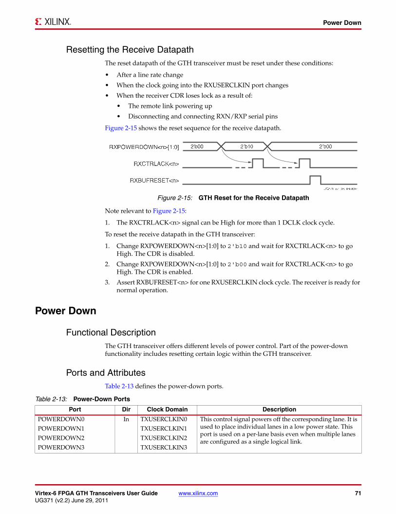
Virtex-6 FPGA GTH Transceivers User Guide www.xilinx.com 71UG371 (v2.2) June 29, 2011
Power Down
Resetting the Receive DatapathThe reset datapath of the GTH transceiver must be reset under these conditions:
• After a line rate change
• When the clock going into the RXUSERCLKIN port changes
• When the receiver CDR loses lock as a result of:
• The remote link powering up
• Disconnecting and connecting RXN/RXP serial pins
Figure 2-15 shows the reset sequence for the receive datapath.
Note relevant to Figure 2-15:
1. The RXCTRLACK<n> signal can be High for more than 1 DCLK clock cycle.
To reset the receive datapath in the GTH transceiver:
1. Change RXPOWERDOWN<n>[1:0] to 2'b10 and wait for RXCTRLACK<n> to go High. The CDR is disabled.
2. Change RXPOWERDOWN<n>[1:0] to 2'b00 and wait for RXCTRLACK<n> to go High. The CDR is enabled.
3. Assert RXBUFRESET<n> for one RXUSERCLKIN clock cycle. The receiver is ready for normal operation.
Power Down
Functional DescriptionThe GTH transceiver offers different levels of power control. Part of the power-down functionality includes resetting certain logic within the GTH transceiver.
Ports and AttributesTable 2-13 defines the power-down ports.
X-Ref Target - Figure 2-15
Figure 2-15: GTH Reset for the Receive Datapath
�����������
�� �� �� �
������������
�����������������
��!�"��#�����
Table 2-13: Power-Down Ports
Port Dir Clock Domain Description
POWERDOWN0
POWERDOWN1
POWERDOWN2
POWERDOWN3
In TXUSERCLKIN0
TXUSERCLKIN1
TXUSERCLKIN2
TXUSERCLKIN3
This control signal powers off the corresponding lane. It is used to place individual lanes in a low power state. This port is used on a per-lane basis even when multiple lanes are configured as a single logical link.

72 www.xilinx.com Virtex-6 FPGA GTH Transceivers User GuideUG371 (v2.2) June 29, 2011
Chapter 2: Shared Transceiver Features
Table 2-14 defines the power-down attributes..
Using Power DownTo activate the power-down mode on a per lane basis, use either the POWERDOWN<n> port or the GTH_CFG_PWRUP_LANE<n> attribute.
The TXPOWERDOWN and RXPOWERDOWN ports are used to activate the power down on the transmitter or the receiver, respectively.
RXPOWERDOWN0[1:0]
RXPOWERDOWN1[1:0]
RXPOWERDOWN2[1:0]
RXPOWERDOWN3[1:0]
In TXUSERCLKIN0
TXUSERCLKIN1
TXUSERCLKIN2
TXUSERCLKIN3
This control signal requests the receiver power state:
00: Normal operation
10: Power-off receiver logic. The PLL continues to operate in this state.
This port must always be set to 2'b10 during initialization and when GTHRESET is asserted.
If the Quad is configured as a x4 link, only the port from Lane 0 is valid.
TXPOWERDOWN0[1:0]
TXPOWERDOWN1[1:0]
TXPOWERDOWN2[1:0]
TXPOWERDOWN3[1:0]
In TXUSERCLKIN0
TXUSERCLKIN1
TXUSERCLKIN2
TXUSERCLKIN3
This control signal requests the transmitter power state:
00: Normal operation
10: Power-off transmitter logic. The PLL continues to operate in this state.
This port must always be set to 2'b10 during initialization and when GTHRESET is asserted.
If the Quad is configured as a x4 link, only the port from Lane 0 is valid.
Table 2-13: Power-Down Ports (Cont’d)
Port Dir Clock Domain Description
Table 2-14: Power-Down Attributes
Attribute Type Description
GTH_CFG_PWRUP_LANE0
GTH_CFG_PWRUP_LANE1
GTH_CFG_PWRUP_LANE2
GTH_CFG_PWRUP_LANE3
1-bit Binary This control attribute powers off the corresponding lane. This attribute is set to 1'b1 to power up the corresponding GTH lane.

Virtex-6 FPGA GTH Transceivers User Guide www.xilinx.com 73UG371 (v2.2) June 29, 2011
Loopback
Loopback
Functional DescriptionThe GTH transceiver supports these loopback modes:
• Far-end Loopback (line loopback)
• Near-end PCS Loopback
• Near-end PMA Loopback
Far-end Loopback
The Far-end loopback mode uses external equipment to generate and check test data. The loopback occurs after passing the deserializer of the PMA. The entire PCS section is bypassed except for the data multiplexers closest to the PMA. The loopback path works only when the external test equipment uses the same reference clock as the PMA.
Figure 2-16 shows the Far-end loopback datapath.
Near-end PCS Loopback
In the Near-end PCS loopback mode, data is generated by user logic and looped back internal to the PCS. Then the data is checked by the user logic. Any PCS operating mode (8B/10B mode, raw mode, etc.) can be used. The PMA is not used.
X-Ref Target - Figure 2-16
Figure 2-16: Far-end Loopback
UG371_c2_09_020510
DFE
PMA
TXN/TXP
RXN/RXP
TXBuffer
RXBuffer
Serializer
Deserializer
PCS
CDR
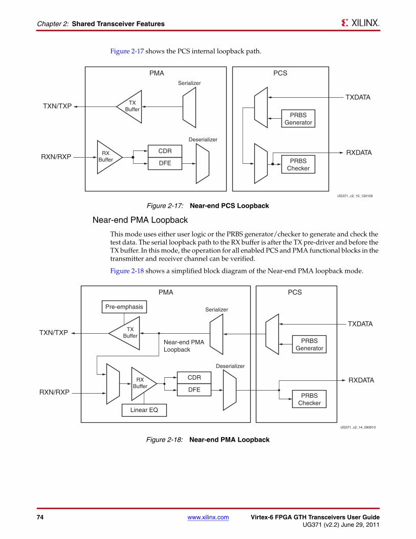
74 www.xilinx.com Virtex-6 FPGA GTH Transceivers User GuideUG371 (v2.2) June 29, 2011
Chapter 2: Shared Transceiver Features
Figure 2-17 shows the PCS internal loopback path.
Near-end PMA Loopback
This mode uses either user logic or the PRBS generator/checker to generate and check the test data. The serial loopback path to the RX buffer is after the TX pre-driver and before the TX buffer. In this mode, the operation for all enabled PCS and PMA functional blocks in the transmitter and receiver channel can be verified.
Figure 2-18 shows a simplified block diagram of the Near-end PMA loopback mode.
X-Ref Target - Figure 2-17
Figure 2-17: Near-end PCS Loopback
DFE
PMA
TXN/TXP
RXDATARXN/RXP
TXBuffer
RXBuffer
Serializer
Deserializer
PCS
UG371_c2_10_120109
CDR
PRBSChecker
TXDATA
PRBSGenerator
X-Ref Target - Figure 2-18
Figure 2-18: Near-end PMA Loopback
DFE
PMA
TXN/TXP
RXDATA
RXN/RXP
TXBuffer
RXBuffer
Serializer
Deserializer
PCS
UG371_c2_14_090910
CDR
Pre-emphasis
Near-end PMALoopback
PRBSChecker
TXDATA
PRBSGenerator
Linear EQ
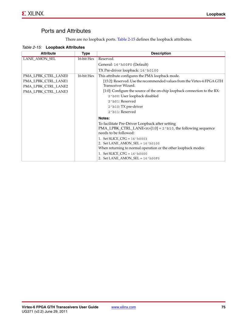
Virtex-6 FPGA GTH Transceivers User Guide www.xilinx.com 75UG371 (v2.2) June 29, 2011
Loopback
Ports and AttributesThere are no loopback ports. Table 2-15 defines the loopback attributes..
Table 2-15: Loopback AttributesAttribute Type Description
LANE_AMON_SEL 16-bit Hex Reserved.
General: 16'h00F0 (Default)
TX Pre-driver loopback: 16'h0100 PMA_LPBK_CTRL_LANE0PMA_LPBK_CTRL_LANE1PMA_LPBK_CTRL_LANE2PMA_LPBK_CTRL_LANE3
16-bit Hex This attribute configures the PMA loopback mode.[15:2]: Reserved. Use the recommended values from the Virtex-6 FPGA GTH Transceiver Wizard.[1:0]: Configure the source of the on-chip loopback connection to the RX:
2’b00: User loopback disabled2’b01: Reserved2’b10: TX pre-driver2’b11: Reserved
Notes: To facilitate Pre-Driver Loopback after setting PMA_LPBK_CTRL_LANE<n>[1:0] = 2'b10, the following sequence needs to be followed:1. Set SLICE_CFG = 16'h0003 2. Set LANE_AMON_SEL = 16'h0100 When returning to normal operation or the other loopback modes:
1. Set SLICE_CFG = 16'h0000 2. Set LANE_AMON_SEL = 16'h00F0

76 www.xilinx.com Virtex-6 FPGA GTH Transceivers User GuideUG371 (v2.2) June 29, 2011
Chapter 2: Shared Transceiver Features
PCS_MODE_LANE0PCS_MODE_LANE1PCS_MODE_LANE2PCS_MODE_LANE3
16-bit Hex This attribute sets the PCS mode.[15]: Loopback serializer/deserializer RX to serializer/deserializer TX[14]: Loopback PCS TX to PCS RX[13:11]: PRBS generator mode
000: None001: PRBS7010: PRBS9011: PRBS11100: PRBS23101: PRBS31Others: Reserved
[10:8]: PRBS checker mode000: None001: PRBS7010: PRBS9011: PRBS11100: PRBS23101: PRBS31Others: Reserved
[7:4]: PCS RX mode0000: Zero 0001: 64B/66B 0111: 8B/10B1010: 16-bit raw data 1011: 20-bit raw data 1100: PRBS Others: Reserved
[3:0]: PCS TX mode0000: Zero 0001: 64B/66B 0111: 8B/10B 1010: 16-bit raw data 1011: 20-bit raw data 1100: PRBS Others: Reserved
SLICE_CFG 16-bit Hex Reserved
General: 16'h0000 (Default)
TX Pre-driver loopback: 16'h0003
Table 2-15: Loopback Attributes (Cont’d)Attribute Type Description

Virtex-6 FPGA GTH Transceivers User Guide www.xilinx.com 77UG371 (v2.2) June 29, 2011
AC-JTAG
AC-JTAG
Functional DescriptionThe Virtex-6 FPGA GTX transceiver supports AC-JTAG, as specified by IEEE Std 1149.6. For JTAG clock operating frequencies specifically in AC-JTAG mode, refer to DS152, Virtex-6 FPGA Data Sheet: DC and Switching Characteristics.
All the GTH transceivers utilized in AC-JTAG testing must be instantiated and initialized in an FPGA design before starting the AC-JTAG test. The recommended procedure is as follows:
1. Configure the FPGA with a design in which all of the following are implemented within the FPGA design:
a. All the utilized GTH transceivers are instantiated.
b. All the utilized GTH transceivers are initialized. For proper initialization of the GTH:
- The reference clock of the correct frequency must be provided
- The DCLK must be provided
- The initialization sequence must be performed as specified in the Reset and Initialization section.
2. Wait for the configured FPGA to complete its GTH initialization sequence. The GTH initialization sequence is indicated by the internal GTH Quad Port GTHINITDONE signal. One solution for ensuring the GTH initialization sequence is complete is for the FPGA design to route the GTHINITDONE signal to a pin that the boundary-scan test tool can sample after the completion of the FPGA configuration procedure. An alternate solution is to wait after the completion of the FPGA configuration procedure for a minimum time. For example, a wait counter of 256,000 TCK cycles can be used as the wait time before starting the AC-JTAG test. The recommendation of 256,000 cycles assumes that the FPGA design is implemented with an internal DCLK of 50 MHz and that the TCK clock of 50 MHz are used.
3. Perform the AC-JTAG test.
Note: The Xilinx BSDLAnno tool must be used to generate a BSDL file that matches the FPGA configuration because the FPGA should be configured for the boundary-scan test. See UG628, Command Line Tools User Guide, available in the ISE® software documentation, for operation of BSDLAnno.

78 www.xilinx.com Virtex-6 FPGA GTH Transceivers User GuideUG371 (v2.2) June 29, 2011
Chapter 2: Shared Transceiver Features
Dynamic Reconfiguration PortFunctional Description
The dynamic reconfiguration port (DRP) allows the dynamic change of parameters of the GTHE1_QUAD primitive. The DRP interface is a processor-friendly synchronous interface with an address bus (DADDR) and separated data buses for reading (DO) and writing (DI) configuration data to the GTH Quad. An enable signal (DEN), a read/write signal (DWE), and a ready/valid signal (DRDY) are the control signals that implement read and write operations, indicate operation completion, or indicate the availability of data. Refer to UG360, Virtex-6 FPGA Configuration User Guide for detailed descriptions and timing diagrams of the DRP operations.
Ports and AttributesTable 2-16 defines the DRP ports.
Using the DRP InterfaceTo enable the DRP interface, the DISABLEDRP port is driven Low. When the DRP interface is enabled, the management interface must be disabled. When a read or write operation is in progress on DRP interfaces, GTHRESET must not be asserted.
Note: When the setting on the DISABLEDRP port is changed to switch between the DRP interface and the management interface, the user must wait two DCLK cycles for the change to take effect before accessing the registers.
Table 2-16: DRP Ports
Port Dir Clock Domain Description
DADDR[15:0] In DCLK This input bus is the DRP address bus.
DCLK In N/A This input is the DRP interface clock. It is also used as the management interface clock when the management interface is enabled. This clock must be connected and available all the time for the GTHE1_QUAD primitive to initialize properly, even if the DRP or the management interface is not used in the design.
DEN In DCLK This input is the DRP enable signal.
0: No read or write operation performed.
1: Enables a read or write operation.
DI[15:0] In DCLK This input bus is the data bus for writing configuration data from the FPGA logic resources to the GTHE1_QUAD primitive.
DISABLEDRP In DCLK This input switches between the DRP and the management interface blocks.
0: DRP interface is selected.
1: Management interface is selected.
DRPDO[15:0] Out DCLK This output bus is the data bus for reading configuration data from the GTHE1_QUAD primitive to the FPGA logic resources.
DRDY Out DCLK When asserted, this output indicates operation is complete for write operations and data is valid for read operations.
DWE In DCLK This input is the DRP write enable:
0: Read operation when DEN is 1.
1: Write operation when DEN is 1.

Virtex-6 FPGA GTH Transceivers User Guide www.xilinx.com 79UG371 (v2.2) June 29, 2011
Management Interface
Management Interface
Functional DescriptionThe management interface allows the dynamic change of parameters of the GTHE1_QUAD primitive. It also allows monitoring the status of certain blocks within the GTH transceiver.
The management interface has separate signals for the MMD, GTH lane, and register address fields. This interface is driven by DCLK. When the management interface is selected, the DRP interface must be disabled by setting the DISABLEDRP port.
Ports and AttributesTable 2-17 defines the management interface ports. There are no management interface attributes..
Table 2-17: Management Interface Ports
Port Dir Clock Domain Description
DCLK In N/A This input is the DRP interface clock. It is also used as the management interface clock when the management interface is enabled. This clock must be connected and available all the time for the GTHE1_QUAD primitive to initialize properly, even if the DRP or the management interface is not used in the design.
DISABLEDRP In DCLK This input switches between the DRP and the management interface blocks.
0: DRP interface is selected.
1: Management interface is selected.
MGMTPCSLANESEL[3:0] In DCLK These inputs select the GTH lane of the management interface:
0001: Select GTH lane 0.
0010: Select GTH lane 1.
0100: Select GTH lane 2.
1000: Select GTH lane 3.
The user can select more than one GTH lane for accessing the registers.
MGMTPCSMMDADDR[4:0] In DCLK This input bus is the MMD address bus.
MGMTPCSRDACK Out DCLK This output is the management interface read data valid signal. It indicates when data is valid for read operations.
MGMTPCSRDDATA[15:0] Out DCLK This output bus is the management interface register read data bus.
MGMTPCSREGADDR[15:0] In DCLK This input bus is the management interface register address bus.
MGMTPCSREGRD In DCLK This input is the management interface read request valid signal.
MGMTPCSREGWR In DCLK This input is the management interface write request valid signal.
MGMTPCSWRDATA[15:0] In DCLK This input bus is the management interface register write data bus.

80 www.xilinx.com Virtex-6 FPGA GTH Transceivers User GuideUG371 (v2.2) June 29, 2011
Chapter 2: Shared Transceiver Features
Using the Management InterfaceTo enable the management interface:
1. Drive the DISABLEDRP port Low during GTH transceiver initialization.
2. When the GTHINITDONE signal goes High from completion of GTH transceiver initialization, drive the DISABLEDRP port High.
One example for implementing the above sequence in logic is to tie the DISABLEDRP port to the inverter of GTHINITDONE.
Note: When the setting on the DISABLEDRP port is changed to switch between the DRP interface and the management interface, the user must wait two DCLK cycles for the change to take effect before accessing the registers.
Figure 2-19 is a timing diagram for reading the register through the management interface.
The read access consists of MMD, GTH lane select, register address signals, and a single cycle pulse of the MGMTPCSREGRD signal. The read addresses must be held until the read access completes and returns an acknowledgment through the MGMTPCSRDACK signal. A read operation can be requested right after the acknowledgment indicator signal as shown in Event 1 of Figure 2-19. No read or write operation can be requested prior to the acknowledgment indicator signal. When a read operation is in progress on MGMT interfaces, GTHRESET must not be asserted.
X-Ref Target - Figure 2-19
Figure 2-19: Management Interface Read Access Timing Diagram
DISABLEDRP
DCLK
MGMTPCSLANESEL[3:0]
MGMTPCSMMDADDR[4:0]
MGMTPCSREGADDR[15:0]
MGMTPCSREGWR
MGMTPCSWRDATA[15:0]
MGMTPCSREGRD
MGMTPCSRDACK
MGMTPCSRDDATA[15:0]
UG371_c2_12_020810
(Select GTH Lane)
(Select MMD Address)
(Select Management Register Address)
16’h0000
(Event 1)
16’h0000

Virtex-6 FPGA GTH Transceivers User Guide www.xilinx.com 81UG371 (v2.2) June 29, 2011
Management Interface
Figure 2-20 is a timing diagram for writing to the register through the management interface.
The write access consists of the MMD, GTH lane select, and register address signals, the write data, and a single cycle pulse of the MGMTPCSREGWR signal. There is no acknowledgment indicator for a write operation. The management interface supports multiple write accesses by asserting the MGMTPCSREGWR signal as shown in Event 1 of Figure 2-20.
Multiple MGMTPCSLANESEL[3:0] signals can be asserted simultaneously for a write access.
X-Ref Target - Figure 2-20
Figure 2-20: Management Interface Write Access Timing Diagram
DISABLEDRP
DCLK
MGMTPCSLANESEL[3:0]
MGMTPCSMMDADDR[4:0]
MGMTPCSREGADDR[15:0]
MGMTPCSREGWR
MGMTPCSWRDATA[15:0]
MGMTPCSREGRD
MGMTPCSRDACK
MGMTPCSRDDATA[15:0]
UG371_c2_13_020810
(Select GTH Lane)
(Select MMD Address)
(Select Management Register Address)
D1 D2 D3
(Event 1)

82 www.xilinx.com Virtex-6 FPGA GTH Transceivers User GuideUG371 (v2.2) June 29, 2011
Chapter 2: Shared Transceiver Features
Differences Between the DRP and Management InterfacesThe DRP interface is a Xilinx standard configuration interface. The management interface is similar to an IEEE MDIO interface. Other considerations when using these interfaces are:
• The DRP interface requires an extra internal logic block to access the PCS/PMA control and status registers. The management interface does not.
• Both the DRP interface and management interface can access and change the settings of the PCS/PMA control registers.
• The DRP interface can access and update the configuration memory space (see Figure 2-21) to retain the setting change after GTHRESET by applying GTHINIT. The management interface can not access or update the configuration memory space. Therefore, any change in the setting of the PCS/PMA registers made by the management interface is not retained after GTHRESET.
• The DRP interface can access the FPGA interconnect data width settings (BUFFER_CONFIG_LANE<n>, TX_FABRIC_WIDTH<n> and RX_FABRIC_WIDTH<n>). The management interface can not be used to access these settings.
X-Ref Target - Figure 2-21
Figure 2-21: DRP and Management Interface (MGMT)
UG371_c2_17_081810
DRP FSM
DRP2MGMT
DISABLEDRP
ConfigurationMemory
PCS and PMAStatus and
ControlRegisters
ManagementI/F
DRPFPGA Interconnect
Data WidthSettings
Virtex-6 FPGA GTH Transceivers User Guide www.xilinx.com 83UG371 (v2.2) June 29, 2011
Chapter 3
Transmitter
This chapter describes how to configure and use each of the functional blocks inside the GTH transmitter (TX). Each GTH transceiver in the GTH Quad includes an independent transmitter, which consists of a PCS and a PMA.
The key elements within the GTH TX are:
• FPGA TX Interface, page 83
• TX 8B/10B Block, page 90
• TX 10 Gigabit Ethernet 64B/66B Block, page 94
• TX Raw Mode, page 97
• TX Pattern Generator, page 102
• TX Polarity Control, page 105
• TX Configurable Driver, page 106
FPGA TX Interface
Functional DescriptionThe FPGA TX interface is the FPGA’s gateway to the TX datapath of the GTH transceiver. Applications transmit data through the GTH transceiver by writing data to the TXDATA port on the positive edge of TXUSERCLKIN. The width of the port can be configured depending on the mode chosen (see Table 3-1).
Table 3-1: FPGA TX Interface Port Width
Mode Port Width
8B/10B mode • 16 bits• 32 bits• 64 bits
64B/66B mode • 64 bits
Raw mode • 16 bits• 20 bits• 32 bits• 40 bits• 64 bits• 80 bits
84 www.xilinx.com Virtex-6 FPGA GTH Transceivers User GuideUG371 (v2.2) June 29, 2011
Chapter 3: Transmitter
The rate of the parallel clock, TXUSERCLKIN, at the interface is determined by the TX line rate, the width of the TXDATA port, and whether or not 8B/10B mode is used. A block inside the PCS handles the mapping of the internal data width to the fabric data width selected in the design.
A data width converter block is included in the transmit datapath. This block includes:
• A clock generator that takes the internal PCS clock and generates TXUSERCLKOUT to the FPGA logic based on the external data width selected
• A four-byte-deep FIFO that handles the phase difference between the internal PCS clock and the external user clock
• A data width converter between the internal PCS data interface and the external data interface to the FPGA logic
The PCS_MODE_LANE<n>[3:0] attribute configures the internal data width, and the TX_FABRIC_WIDTH<n> attribute configures the external data width. Table 3-2 shows how the interface width for the TX datapath is selected..
Table 3-2: FPGA TX Interface Datapath Configuration
TX Data ModeInternal PCS Data
WidthFabric Interface
Data WidthPCS_MODE_LANE<n>[3:0] TX_FABRIC_WIDTH<n>
8B/10B 20 bits 16 bits 0111 16
20 bits 32 bits 0111 32
20 bits 64 bits 0111 64
64B/66B 64 bits 64 bits 0001 6466
Raw 16 bits 16 bits 1010 16
16 bits 32 bits 1010 32
16 bits 64 bits 1010 64
20 bits 20 bits 1011 20
20 bits 40 bits 1011 40
20 bits 80 bits 1011 80
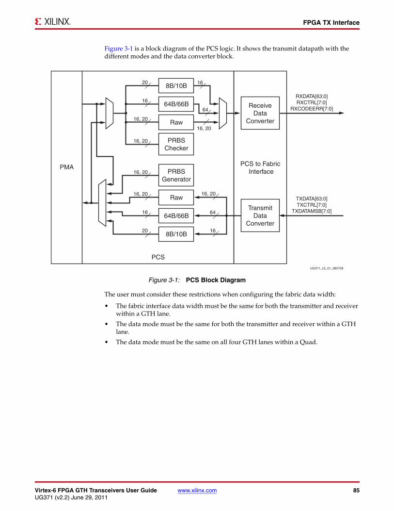
Virtex-6 FPGA GTH Transceivers User Guide www.xilinx.com 85UG371 (v2.2) June 29, 2011
FPGA TX Interface
Figure 3-1 is a block diagram of the PCS logic. It shows the transmit datapath with the different modes and the data converter block.
The user must consider these restrictions when configuring the fabric data width:
• The fabric interface data width must be the same for both the transmitter and receiver within a GTH lane.
• The data mode must be the same for both the transmitter and receiver within a GTH lane.
• The data mode must be the same on all four GTH lanes within a Quad.
X-Ref Target - Figure 3-1
Figure 3-1: PCS Block Diagram
UG371_c3_01_082709
RXDATA[63:0]RXCTRL[7:0]
RXCODEERR[7:0]
8B/10B
64B/66B
Raw
PRBSChecker
ReceiveData
Converter
PCS to Fabric Interface
PCS
PMA
20
20
16
16
64
16, 20
16, 20
64
16
16, 20
16, 20
TXDATA[63:0]TXCTRL[7:0]
TXDATAMSB[7:0]
Raw
64B/66B
8B/10B
PRBSGenerator
TransmitData
Converter
16, 20
16, 20
16
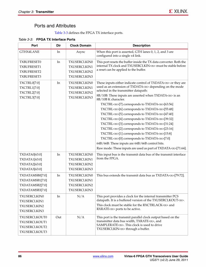
86 www.xilinx.com Virtex-6 FPGA GTH Transceivers User GuideUG371 (v2.2) June 29, 2011
Chapter 3: Transmitter
Ports and AttributesTable 3-3 defines the FPGA TX interface ports.
Table 3-3: FPGA TX Interface Ports
Port Dir Clock Domain Description
GTHX4LANE In Async When this port is asserted, GTH lanes 0, 1, 2, and 3 are configured into a single x4 link.
TXBUFRESET0
TXBUFRESET1
TXBUFRESET2
TXBUFRESET3
In TXUSERCLKIN0
TXUSERCLKIN1
TXUSERCLKIN2
TXUSERCLKIN3
This port resets the buffer inside the TX data converter. Both the internal TX clock and TXUSERCLKIN<n> must be stable before a reset can be applied to the buffer.
TXCTRL0[7:0]
TXCTRL1[7:0]
TXCTRL2[7:0]
TXCTRL3[7:0]
In TXUSERCLKIN0
TXUSERCLKIN1
TXUSERCLKIN2
TXUSERCLKIN3
These inputs either indicate control of TXDATA<n> or they are used as an extension of TXDATA<n> depending on the mode selected in the transmitter datapath:
8B/10B: These inputs are asserted when TXDATA<n> is an 8B/10B K character.
TXCTRL<n>[7] corresponds to TXDATA<n>[63:56]
TXCTRL<n>[6] corresponds to TXDATA<n>[55:48]
TXCTRL<n>[5] corresponds to TXDATA<n>[47:40]
TXCTRL<n>[4] corresponds to TXDATA<n>[39:32]
TXCTRL<n>[3] corresponds to TXDATA<n>[31:24]
TXCTRL<n>[2] corresponds to TXDATA<n>[23:16]
TXCTRL<n>[1] corresponds to TXDATA<n>[15:8]
TXCTRL<n>[0] corresponds to TXDATA<n>[7:0]
64B/66B: These inputs are 64B/66B control bits.
Raw mode: These inputs are used as part of TXDATA<n>[71:64].
TXDATA0[63:0]
TXDATA1[63:0]
TXDATA2[63:0]
TXDATA3[63:0]
In TXUSERCLKIN0
TXUSERCLKIN1
TXUSERCLKIN2
TXUSERCLKIN3
This input bus is the transmit data bus of the transmit interface from the FPGA.
TXDATAMSB0[7:0]
TXDATAMSB1[7:0]
TXDATAMSB2[7:0]
TXDATAMSB3[7:0]
In TXUSERCLKIN0
TXUSERCLKIN1
TXUSERCLKIN2
TXUSERCLKIN3
This bus extends the transmit data bus as TXDATA<n>[79:72].
TXUSERCLKIN0
TXUSERCLKIN1
TXUSERCLKIN2
TXUSERCLKIN3
In N/A This port provides a clock for the internal transmitter PCS datapath. It is a buffered version of the TXUSERCLKOUT<n>.
This clock must be stable for the RXCTRLACK<n> and RXRATE<n> ports to be active.
TXUSERCLKOUT0
TXUSERCLKOUT1
TXUSERCLKOUT2
TXUSERCLKOUT3
Out N/A This port is the transmit parallel clock output based on the transmitter data bus width, TXRATE<n>, and SAMPLERATE<n>. This clock is used to drive TXUSERCLKIN<n> through a buffer.

Virtex-6 FPGA GTH Transceivers User Guide www.xilinx.com 87UG371 (v2.2) June 29, 2011
FPGA TX Interface
Table 3-4 defines the FPGA TX interface attributes.
Table 3-4: FPGA TX Interface Attributes
Attribute Type Description
BUFFER_CONFIG_LANE0
BUFFER_CONFIG_LANE1
BUFFER_CONFIG_LANE2
BUFFER_CONFIG_LANE3
16-bit Hex This attribute defaults to 16’h4004.
[15:4]: TX_BUFFER_CONFIG[11:0] read pointer adjustment for TX buffer in the data converter.
• For auto adjustment mode, TX_BUFFER_CONFIG[11:0] = 12’h400.
• For manual adjustment mode, TX_BUFFER_CONFIG[11:0] settings depend on TX_FABRIC_WIDTH and if the GTH transceivers within a Quad are configured as a x4 link (GTHX4LANE = 1’b1):• x4 (GTHX4LANE = 1’b1): [TX_FABRIC_WIDTH] = [TX_BUFFER_CONFIG]
“16” or “20” (DRP value 3'b000): 12’h0A4
“32” (DRP value 3'b011): 12’h394
“40” (DRP value 3'b101): 12’h394
“64” (DRP value 3'b010): 12’h250
“80” (DRP value 3'b110): 12’h250
“6466” (DRP value 3'b111): 12’h0A4
• x1 (GTHX4LANE = 1’b0): [TX_FABRIC_WIDTH] = [TX_BUFFER_CONFIG]
“16” or “20” (DRP value 3'b000): 12’h23C
“32” (DRP value 3'b011): 12’h0E8
“40” (DRP value 3'b101): 12’h0E8
“64” (DRP value 3'b010): 12’h3A8
“80” (DRP value 3'b110): 12’h3A8
“6466” (DRP value 3'b111): 12’h23C
[4:0]: RX_BUFFER_CONFIG[3:0] read pointer adjustment for RX buffer in the data converter.
• For auto adjustment mode, RX_BUFFER_CONFIG[3:0] = 0100.• For manual adjustment mode, RX_BUFFER_CONFIG[3:0] settings
depend on the RX_FABRIC_WIDTH:
[RX_FABRIC_WIDTH] = [RX_BUFFER_CONFIG]
“16” or “20” (DRP value 3'b000): 4’b0001
“32” (DRP value 3'b011): 4’b0000
“40” (DRP value 3'b101): 4’b0000
“64” (DRP value 3'b010): 4’b0000
“80” (DRP value 3'b110): 4’b0000
“6466” (DRP value 3'b111): 4’b0001
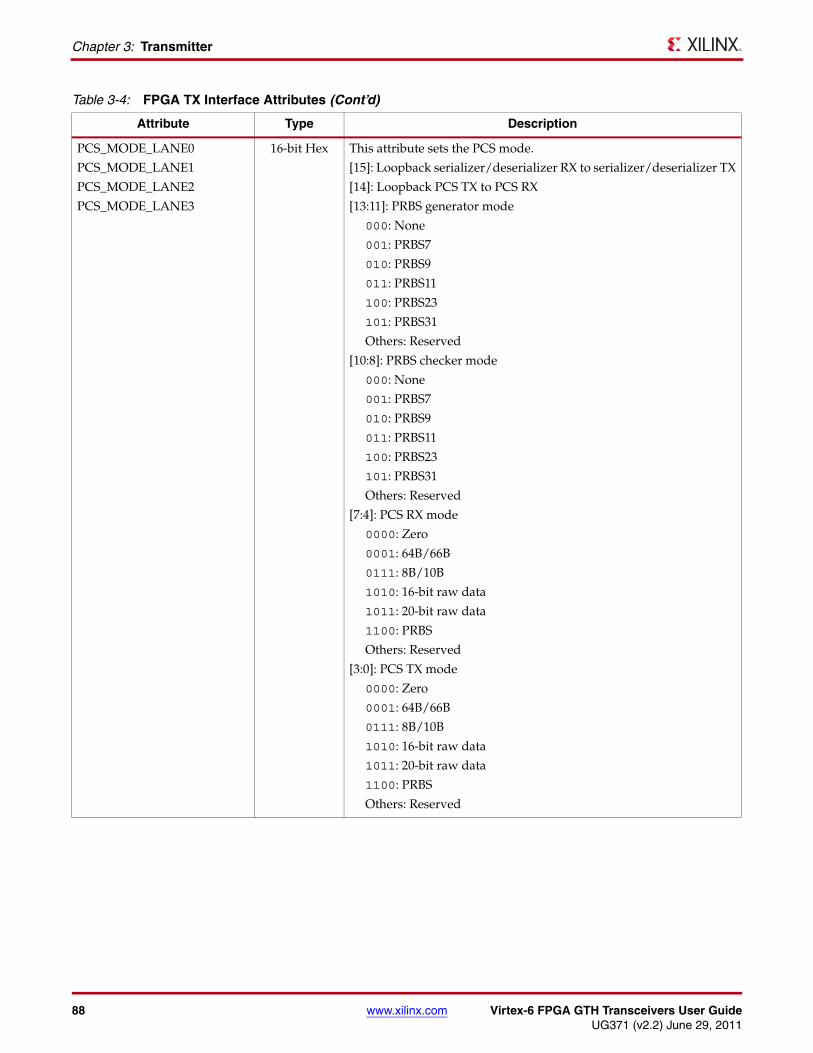
88 www.xilinx.com Virtex-6 FPGA GTH Transceivers User GuideUG371 (v2.2) June 29, 2011
Chapter 3: Transmitter
PCS_MODE_LANE0
PCS_MODE_LANE1
PCS_MODE_LANE2
PCS_MODE_LANE3
16-bit Hex This attribute sets the PCS mode.
[15]: Loopback serializer/deserializer RX to serializer/deserializer TX
[14]: Loopback PCS TX to PCS RX
[13:11]: PRBS generator mode
000: None
001: PRBS7
010: PRBS9
011: PRBS11
100: PRBS23
101: PRBS31
Others: Reserved
[10:8]: PRBS checker mode
000: None
001: PRBS7
010: PRBS9
011: PRBS11
100: PRBS23
101: PRBS31
Others: Reserved
[7:4]: PCS RX mode
0000: Zero
0001: 64B/66B
0111: 8B/10B
1010: 16-bit raw data
1011: 20-bit raw data
1100: PRBS
Others: Reserved
[3:0]: PCS TX mode
0000: Zero
0001: 64B/66B
0111: 8B/10B
1010: 16-bit raw data
1011: 20-bit raw data
1100: PRBS
Others: Reserved
Table 3-4: FPGA TX Interface Attributes (Cont’d)
Attribute Type Description
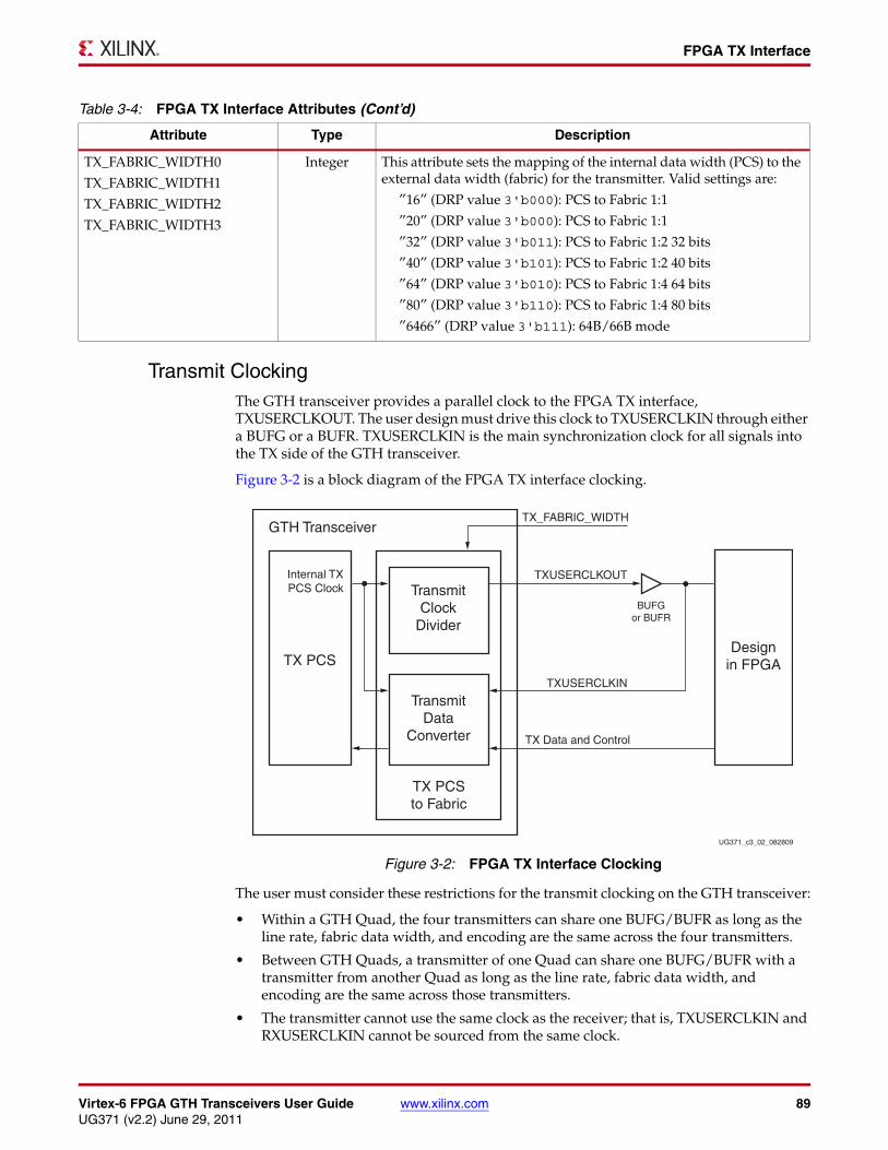
Virtex-6 FPGA GTH Transceivers User Guide www.xilinx.com 89UG371 (v2.2) June 29, 2011
FPGA TX Interface
Transmit ClockingThe GTH transceiver provides a parallel clock to the FPGA TX interface, TXUSERCLKOUT. The user design must drive this clock to TXUSERCLKIN through either a BUFG or a BUFR. TXUSERCLKIN is the main synchronization clock for all signals into the TX side of the GTH transceiver.
Figure 3-2 is a block diagram of the FPGA TX interface clocking.
The user must consider these restrictions for the transmit clocking on the GTH transceiver:
• Within a GTH Quad, the four transmitters can share one BUFG/BUFR as long as the line rate, fabric data width, and encoding are the same across the four transmitters.
• Between GTH Quads, a transmitter of one Quad can share one BUFG/BUFR with a transmitter from another Quad as long as the line rate, fabric data width, and encoding are the same across those transmitters.
• The transmitter cannot use the same clock as the receiver; that is, TXUSERCLKIN and RXUSERCLKIN cannot be sourced from the same clock.
TX_FABRIC_WIDTH0
TX_FABRIC_WIDTH1
TX_FABRIC_WIDTH2
TX_FABRIC_WIDTH3
Integer This attribute sets the mapping of the internal data width (PCS) to the external data width (fabric) for the transmitter. Valid settings are:
”16” (DRP value 3'b000): PCS to Fabric 1:1
”20” (DRP value 3'b000): PCS to Fabric 1:1
”32” (DRP value 3'b011): PCS to Fabric 1:2 32 bits
”40” (DRP value 3'b101): PCS to Fabric 1:2 40 bits
”64” (DRP value 3'b010): PCS to Fabric 1:4 64 bits
”80” (DRP value 3'b110): PCS to Fabric 1:4 80 bits
”6466” (DRP value 3'b111): 64B/66B mode
Table 3-4: FPGA TX Interface Attributes (Cont’d)
Attribute Type Description
X-Ref Target - Figure 3-2
Figure 3-2: FPGA TX Interface Clocking
UG371_c3_02_082809
Internal TXPCS Clock
TX_FABRIC_WIDTH
TXUSERCLKOUT
TXUSERCLKIN
TX Data and Control
TX PCS
TX PCSto Fabric
Designin FPGA
TransmitClock
Divider
TransmitData
Converter
GTH Transceiver
BUFGor BUFR

90 www.xilinx.com Virtex-6 FPGA GTH Transceivers User GuideUG371 (v2.2) June 29, 2011
Chapter 3: Transmitter
Configuring the Transmitter for Multi-lane ApplicationsThe GTHX4LANE port in GTH transceivers is used for multi-lane applications that require minimum skew across channels. To configure four GTH lanes within a Quad into a single x4 link, GTHX4LANE must be tied High. When configured in a single x4 link, a change in the control settings on the master lane also causes the same effect on the slaves. An exception to this is the POWERDOWN port. In this x4 link configuration, the buffers across the four transmit data converter are synchronized for minimizing skew.
TX 8B/10B Block
Functional DescriptionMany protocols use 8B/10B encoding on outgoing data. 8B/10B is an industry-standard encoding scheme that trades two bits of overhead per byte for improved performance. The GTH transceiver includes an 8B/10B encoder to encode TX data without consuming FPGA resources.
Ports and AttributesTable 3-5 defines the TX 8B/10B block ports..
Table 3-5: TX 8B/10B Block Ports
Port Dir Clock Domain Description
TXCTRL0[7:0]
TXCTRL1[7:0]
TXCTRL2[7:0]
TXCTRL3[7:0]
In TXUSERCLKIN0
TXUSERCLKIN1
TXUSERCLKIN2
TXUSERCLKIN3
These inputs indicate control of TXDATA<n> or they are used as an extension of TXDATA<n> depending on the mode selected in the transmitter datapath:
8B/10B: These inputs are asserted when TXDATA<n> is an 8B/10B K character.
TXCTRL<n>[7] corresponds to TXDATA<n>[63:56]
TXCTRL<n>[6] corresponds to TXDATA<n>[55:48]
TXCTRL<n>[5] corresponds to TXDATA<n>[47:40]
TXCTRL<n>[4] corresponds to TXDATA<n>[39:32]
TXCTRL<n>[3] corresponds to TXDATA<n>[31:24]
TXCTRL<n>[2] corresponds to TXDATA<n>[23:16]
TXCTRL<n>[1] corresponds to TXDATA<n>[15:8]
TXCTRL<n>[0] corresponds to TXDATA<n>[7:0]
64B/66B: These inputs are 64B/66B control bits.
Raw mode: These inputs are used as part of TXDATA<n>[71:64].
TXDATA0[63:0]
TXDATA1[63:0]
TXDATA2[63:0]
TXDATA3[63:0]
In TXUSERCLKIN0
TXUSERCLKIN1
TXUSERCLKIN2
TXUSERCLKIN3
This input bus is the transmit data bus of the transmit interface from the FPGA.
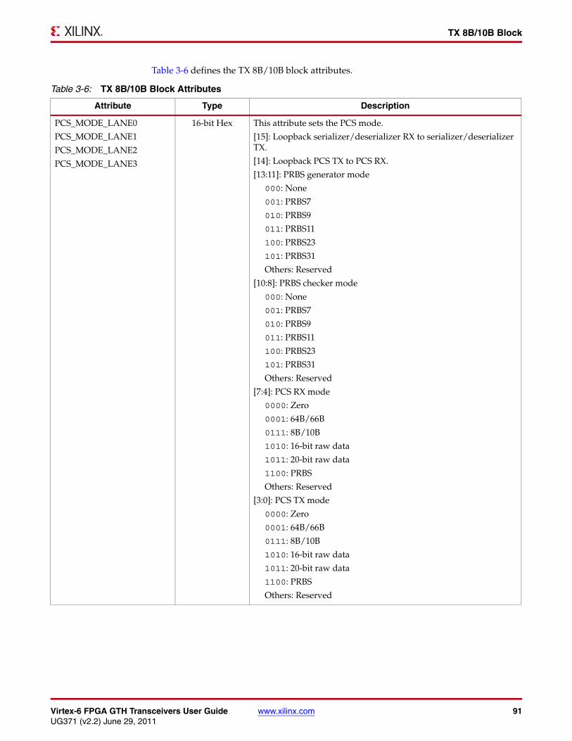
Virtex-6 FPGA GTH Transceivers User Guide www.xilinx.com 91UG371 (v2.2) June 29, 2011
TX 8B/10B Block
Table 3-6 defines the TX 8B/10B block attributes.
Table 3-6: TX 8B/10B Block Attributes
Attribute Type Description
PCS_MODE_LANE0
PCS_MODE_LANE1
PCS_MODE_LANE2
PCS_MODE_LANE3
16-bit Hex This attribute sets the PCS mode.
[15]: Loopback serializer/deserializer RX to serializer/deserializer TX.
[14]: Loopback PCS TX to PCS RX.
[13:11]: PRBS generator mode
000: None
001: PRBS7
010: PRBS9
011: PRBS11
100: PRBS23
101: PRBS31
Others: Reserved
[10:8]: PRBS checker mode
000: None
001: PRBS7
010: PRBS9
011: PRBS11
100: PRBS23
101: PRBS31
Others: Reserved
[7:4]: PCS RX mode
0000: Zero
0001: 64B/66B
0111: 8B/10B
1010: 16-bit raw data
1011: 20-bit raw data
1100: PRBS
Others: Reserved
[3:0]: PCS TX mode
0000: Zero
0001: 64B/66B
0111: 8B/10B
1010: 16-bit raw data
1011: 20-bit raw data
1100: PRBS
Others: Reserved

92 www.xilinx.com Virtex-6 FPGA GTH Transceivers User GuideUG371 (v2.2) June 29, 2011
Chapter 3: Transmitter
PCS_RESET_LANE0
PCS_RESET_LANE1
PCS_RESET_LANE2
PCS_RESET_LANE3
16-bit Hex This attribute controls the datapath resets. It varies by mode:
64B/66B: 0xF3FE
8B/10B: 0xFC5B
Raw: 0xFF3B
PRBS: 0xFFCE
Default: 0xFFFF
[15:12]: Reserved
[11]: Reset 64B/66B receive
[10]: Reset 64B/66B transmit
[9]: Reset 8B/10B receive
[8]: Reset 8B/10B transmit
[7]: Reset RX FIFO
[6]: Reset RX Raw FIFO
[5]: Reset PRBS checker
[4]: Reset PRBS generator
[3]: Reserved
[2]: Reset 8B/10B TX FIFO
[1]: Reset RX loopback FIFO
[0]: Reset 64B/66B and PRBS TX FIFO
PCS_RESET_1_LANE0
PCS_RESET_1_LANE1
PCS_RESET_1_LANE2
PCS_RESET_1_LANE3
16-bit Hex [15:2]: Reserved. Use the recommended values from theVirtex-6 FPGA GTH Transceiver Wizard.
[1:0]: This attribute controls the datapath resets. It varies by mode:
64B/66B: 2'b10
8B/10B: 2'b00
Raw: 2'b00
PRBS: 2'b10
Default: 2'b11
TX_FABRIC_WIDTH0
TX_FABRIC_WIDTH1
TX_FABRIC_WIDTH2
TX_FABRIC_WIDTH3
Integer This attribute sets the mapping of the internal data width (PCS) to the external data width (fabric) for the transmitter. Valid settings are:
”16” (DRP value 3'b000): PCS to Fabric 1:1
”20” (DRP value 3'b000): PCS to Fabric 1:1
”32” (DRP value 3'b011): PCS to Fabric 1:2 32 bits
”40” (DRP value 3'b101): PCS to Fabric 1:2 40 bits
”64” (DRP value 3'b010): PCS to Fabric 1:4 64 bits
”80” (DRP value 3'b110): PCS to Fabric 1:4 80 bits
”6466” (DRP value 3'b111): 64B/66B mode
Table 3-6: TX 8B/10B Block Attributes (Cont’d)
Attribute Type Description
Virtex-6 FPGA GTH Transceivers User Guide www.xilinx.com 93UG371 (v2.2) June 29, 2011
TX 8B/10B Block
Enabling 8B/10B ModeFollow these steps to enable the 8B/10B mode in the GTH transmitter:
1. Set PCS_MODE_LANE<n>[3:0] to 4'b0111.
2. Set PCS_RESET_LANE<n> to 0xFC5B.
• Set PCS_RESET_1_LANE<n>[1:0] to 2'b00.
• Set TX_FABRIC_WIDTH<n> to either “16”, “32”, or “64” depending on the application.
The 8B/10B table includes special characters (K characters) that are often used for control functions. To transmit TXDATA as a K character instead of regular data, the TXCTRL port must be driven High.

94 www.xilinx.com Virtex-6 FPGA GTH Transceivers User GuideUG371 (v2.2) June 29, 2011
Chapter 3: Transmitter
TX 10 Gigabit Ethernet 64B/66B Block
Functional DescriptionSome high-speed data rate protocols use 64B/66B encoding to reduce the overhead of 8B/10B encoding while retaining the benefits of an encoding scheme. The GTH transceiver implements the 64B/66B block based on the IEEE 802.3-2008 Clause 49, “Physical Sublayer (PCS) for 64B/66B, type 10GBASE-R.” The transmit 64B/66B block includes the scrambler and the gearbox.
Ports and AttributesTable 3-7 defines the TX 10 Gb Ethernet 64B/66B block ports.
Table 3-7: TX 10 10 Gb Ethernet 64B/66B Block Ports
Port Dir Clock Domain Description
TXCTRL0[7:0]
TXCTRL1[7:0]
TXCTRL2[7:0]
TXCTRL3[7:0]
In TXUSERCLKIN0
TXUSERCLKIN1
TXUSERCLKIN2
TXUSERCLKIN3
These inputs indicate control of TXDATA<n> or they are used as an extension of TXDATA<n> depending on the mode selected in the transmitter datapath:
8B/10B: These inputs are asserted when TXDATA<n> is an 8B/10B K character.
TXCTRL<n>[7] corresponds to TXDATA<n>[63:56]
TXCTRL<n>[6] corresponds to TXDATA<n>[55:48]
TXCTRL<n>[5] corresponds to TXDATA<n>[47:40]
TXCTRL<n>[4] corresponds to TXDATA<n>[39:32]
TXCTRL<n>[3] corresponds to TXDATA<n>[31:24]
TXCTRL<n>[2] corresponds to TXDATA<n>[23:16]
TXCTRL<n>[1] corresponds to TXDATA<n>[15:8]
TXCTRL<n>[0] corresponds to TXDATA<n>[7:0]
64B/66B: These inputs are 64B/66B control bits.
Raw mode: These inputs are used as part of TXDATA<n>[71:64].
TXDATA0[63:0]
TXDATA1[63:0]
TXDATA2[63:0]
TXDATA3[63:0]
In TXUSERCLKIN0
TXUSERCLKIN1
TXUSERCLKIN2
TXUSERCLKIN3
This input bus is the transmit data bus of the transmit interface from the FPGA.

Virtex-6 FPGA GTH Transceivers User Guide www.xilinx.com 95UG371 (v2.2) June 29, 2011
TX 10 Gigabit Ethernet 64B/66B Block
Table 3-8 defines the TX 10 Gb Ethernet 64B/66B block attributes.
Table 3-8: TX 10 10 Gb Ethernet 64B/66B Block Attributes
Attribute Type Description
PCS_MODE_LANE0
PCS_MODE_LANE1
PCS_MODE_LANE2
PCS_MODE_LANE3
16-bit Hex This attribute sets the PCS mode.
[15]: Loopback serializer/deserializer RX to serializer/deserializer TX.
[14]: Loopback PCS TX to PCS RX.
[13:11]: PRBS generator mode
000: None
001: PRBS7
010: PRBS9
011: PRBS11
100: PRBS23
101: PRBS31
Others: Reserved
[10:8]: PRBS checker mode
000: None
001: PRBS7
010: PRBS9
011: PRBS11
100: PRBS23
101: PRBS31
Others: Reserved
[7:4]: PCS RX mode
0000: Zero
0001: 64B/66B
0111: 8B/10B
1010: 16-bit raw data
1011: 20-bit raw data
1100: PRBS
Others: Reserved
[3:0]: PCS TX mode
0000: Zero
0001: 64B/66B
0111: 8B/10B
1010: 16-bit raw data
1011: 20-bit raw data
1100: PRBS
Others: Reserved
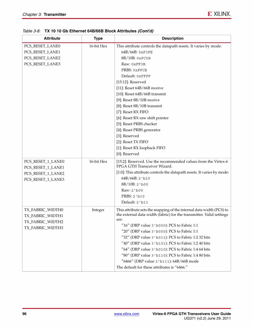
96 www.xilinx.com Virtex-6 FPGA GTH Transceivers User GuideUG371 (v2.2) June 29, 2011
Chapter 3: Transmitter
PCS_RESET_LANE0
PCS_RESET_LANE1
PCS_RESET_LANE2
PCS_RESET_LANE3
16-bit Hex This attribute controls the datapath resets. It varies by mode:
64B/66B: 0xF3FE
8B/10B: 0xFC5B
Raw: 0xFF3B
PRBS: 0xFFCE
Default: 0xFFFF
[15:12]: Reserved
[11]: Reset 64B/66B receive
[10]: Reset 64B/66B transmit
[9]: Reset 8B/10B receive
[8]: Reset 8B/10B transmit
[7]: Reset RX FIFO
[6]: Reset RX raw shift pointer
[5]: Reset PRBS checker
[4]: Reset PRBS generator
[3]: Reserved
[2]: Reset TX FIFO
[1]: Reset RX loopback FIFO
[0]: Reserved
PCS_RESET_1_LANE0
PCS_RESET_1_LANE1
PCS_RESET_1_LANE2
PCS_RESET_1_LANE3
16-bit Hex [15:2]: Reserved. Use the recommended values from the Virtex-6 FPGA GTH Transceiver Wizard.
[1:0]: This attribute controls the datapath resets. It varies by mode:
64B/66B: 2'b10
8B/10B: 2'b00
Raw: 2'b00
PRBS: 2'b10
Default: 2'b11
TX_FABRIC_WIDTH0
TX_FABRIC_WIDTH1
TX_FABRIC_WIDTH2
TX_FABRIC_WIDTH3
Integer This attribute sets the mapping of the internal data width (PCS) to the external data width (fabric) for the transmitter. Valid settings are:
”16” (DRP value 3'b000): PCS to Fabric 1:1
”20” (DRP value 3'b000): PCS to Fabric 1:1
”32” (DRP value 3'b011): PCS to Fabric 1:2 32 bits
”40” (DRP value 3'b101): PCS to Fabric 1:2 40 bits
”64” (DRP value 3'b010): PCS to Fabric 1:4 64 bits
”80” (DRP value 3'b110): PCS to Fabric 1:4 80 bits
”6466” (DRP value 3'b111): 64B/66B mode
The default for these attributes is “6466.”
Table 3-8: TX 10 10 Gb Ethernet 64B/66B Block Attributes (Cont’d)
Attribute Type Description
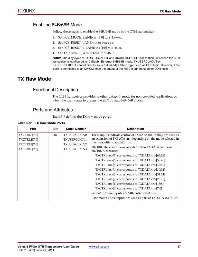
Virtex-6 FPGA GTH Transceivers User Guide www.xilinx.com 97UG371 (v2.2) June 29, 2011
TX Raw Mode
Enabling 64B/66B ModeFollow these steps to enable the 64B/66B mode in the GTH transmitter:
1. Set PCS_MODE_LANE<n>[3:0] to 4'b0001.
2. Set PCS_RESET_LANE<n> to 0xF3FE.
3. Set PCS_RESET_1_LANE<n>[1:0] to 2'b10.
4. Set TX_FABRIC_WIDTH<n> to “6466.”
Note: The duty cycle of TXUSERCLKOUT and RXUSERCLKOUT is less than 30% when the GTH transceiver is configured in10 Gigabit Ethernet 64B/66B mode. TXUSERCLKOUT or RXUSERCLKOUT cannot directly source dual-edge fabric logic, such as DDR logic. However, if the clock is connected to an MMCM, then the output of the MMCM can be used for DDR logic.
TX Raw Mode
Functional DescriptionThe GTH transceiver provides another datapath mode for non-encoded applications or when the user wants to bypass the 8B/10B and 64B/66B blocks.
Ports and AttributesTable 3-9 defines the TX raw mode ports.
Table 3-9: TX Raw Mode Ports
Port Dir Clock Domain Description
TXCTRL0[7:0]
TXCTRL1[7:0]
TXCTRL2[7:0]
TXCTRL3[7:0]
In TXUSERCLKIN0
TXUSERCLKIN1
TXUSERCLKIN2
TXUSERCLKIN3
These inputs indicate control of TXDATA<n> or they are used as an extension of TXDATA<n> depending on the mode selected in the transmitter datapath:
8B/10B: These inputs are asserted when TXDATA<n> is an 8B/10B K character.
TXCTRL<n>[7] corresponds to TXDATA<n>[63:56]
TXCTRL<n>[6] corresponds to TXDATA<n>[55:48]
TXCTRL<n>[5] corresponds to TXDATA<n>[47:40]
TXCTRL<n>[4] corresponds to TXDATA<n>[39:32]
TXCTRL<n>[3] corresponds to TXDATA<n>[31:24]
TXCTRL<n>[2] corresponds to TXDATA<n>[23:16]
TXCTRL<n>[1] corresponds to TXDATA<n>[15:8]
TXCTRL<n>[0] corresponds to TXDATA<n>[7:0]
64B/66B: These inputs are 64B/66B control bits.
Raw mode: These inputs are used as part of TXDATA<n>[71:64].

98 www.xilinx.com Virtex-6 FPGA GTH Transceivers User GuideUG371 (v2.2) June 29, 2011
Chapter 3: Transmitter
TXDATA0[63:0]
TXDATA1[63:0]
TXDATA2[63:0]
TXDATA3[63:0]
In TXUSERCLKIN0
TXUSERCLKIN1
TXUSERCLKIN2
TXUSERCLKIN3
This input bus is the transmit data bus of the transmit interface from the FPGA.
TXDATAMSB0[7:0]
TXDATAMSB1[7:0]
TXDATAMSB2[7:0]
TXDATAMSB3[7:0]
In TXUSERCLKIN0
TXUSERCLKIN1
TXUSERCLKIN2
TXUSERCLKIN3
This bus extends the transmit data bus as TXDATA<n>[79:72].
Table 3-9: TX Raw Mode Ports (Cont’d)
Port Dir Clock Domain Description

Virtex-6 FPGA GTH Transceivers User Guide www.xilinx.com 99UG371 (v2.2) June 29, 2011
TX Raw Mode
Table 3-10 defines the TX raw mode attributes.
Table 3-10: TX Raw Mode Attributes
Attribute Type Description
PCS_MODE_LANE0
PCS_MODE_LANE1
PCS_MODE_LANE2
PCS_MODE_LANE3
16-bit Hex This attribute sets the PCS mode.
[15]: Loopback serializer/deserializer RX to serializer/deserializer TX
[14]: Loopback PCS TX to PCS RX
[13:11]: PRBS generator mode
000: None
001: PRBS7
010: PRBS9
011: PRBS11
100: PRBS23
101: PRBS31
Others: Reserved
[10:8]: PRBS checker mode
000: None
001: PRBS7
010: PRBS9
011: PRBS11
100: PRBS23
101: PRBS31
Others: Reserved
[7:4]: PCS RX mode
0000: Zero
0001: 64B/66B
0111: 8B/10B
1010: 16-bit raw data
1011: 20-bit raw data
1100: PRBS
Others: Reserved
[3:0]: PCS TX mode
0000: Zero
0001: 64B/66B
0111: 8B/10B
1010: 16-bit raw data
1011: 20-bit raw data
1100: PRBS
Others: Reserved

100 www.xilinx.com Virtex-6 FPGA GTH Transceivers User GuideUG371 (v2.2) June 29, 2011
Chapter 3: Transmitter
PCS_RESET_LANE0
PCS_RESET_LANE1
PCS_RESET_LANE2
PCS_RESET_LANE3
16-bit Hex This attribute controls the datapath resets. It varies by mode:
64B/66B: 0xF3FE
8B/10B: 0xFC5B
Raw: 0xFF3B
PRBS: 0xFFCE
Default: 0xFFFF
[15:12]: Reserved
[11]: Reset 64B/66B receive
[10]: Reset 64B/66B transmit
[9]: Reset 8B/10B receive
[8]: Reset 8B/10B transmit
[7]: Reset RX FIFO
[6]: Reset RX raw shift pointer
[5]: Reset PRBS checker
[4]: Reset PRBS generator
[3]: Reserved
[2]: Reset TX FIFO
[1]: Reset RX loopback FIFO
[0]: Reserved
PCS_RESET_1_LANE0
PCS_RESET_1_LANE1
PCS_RESET_1_LANE2
PCS_RESET_1_LANE3
16-bit Hex [15:2]: Reserved. Use the recommended values from the Virtex-6 FPGA GTH Transceiver Wizard.
[1:0]: This attribute controls the datapath resets. It varies by mode:
64B/66B: 2'b10
8B/10B: 2'b00
Raw: 2'b00
PRBS: 2'b10
Default: 2'b11
TX_FABRIC_WIDTH0
TX_FABRIC_WIDTH1
TX_FABRIC_WIDTH2
TX_FABRIC_WIDTH3
Integer Defaults to “6466.”This attribute sets the mapping of the internal data width (PCS) to the external data width (fabric) for the transmitter. Valid settings are:
“16” (DRP value 3'b000): PCS to Fabric 1:1
“20” (DRP value 3'b000): PCS to Fabric 1:1
“32” (DRP value 3'b011): PCS to Fabric 1:2 32 bits
“40” (DRP value 3'b101): PCS to Fabric 1:2 40 bits
“64” (DRP value 3'b010): PCS to Fabric 1:4 64 bits
“80” (DRP value 3'b110): PCS to Fabric 1:4 80 bits
“6466” (DRP value 3'b111): 64B/66B mode
Table 3-10: TX Raw Mode Attributes (Cont’d)
Attribute Type Description
Virtex-6 FPGA GTH Transceivers User Guide www.xilinx.com 101UG371 (v2.2) June 29, 2011
TX Raw Mode
Enabling Raw ModeFollow these steps to enable the Raw mode in the GTH transmitter:
1. If the transmit fabric data width is configured to 16 bits, 32 bits, or 64 bits
a. Set PCS_MODE_LANE<n>[3:0] to 4'b1010.
b. Set PCS_RESET_LANE<n> to 0xFF3B.
c. Set PCS_RESET_1_LANE<n>[1:0] to 2'b00.
d. Set TX_FABRIC_WIDTH<n> to “16”, “32”, or “64.”
2. If the transmit fabric data width is configured to 20 bits, 40 bits, or 80 bits
a. Set PCS_MODE_LANE<n>[3:0] to 4'b1011.
b. Set PCS_RESET_LANE<n> to 0xFF3B.
c. Set PCS_RESET_1_LANE<n>[1:0] to 2'b00.
d. Set TX_FABRIC_WIDTH<n> to “20”, “40”, or “80.”

102 www.xilinx.com Virtex-6 FPGA GTH Transceivers User GuideUG371 (v2.2) June 29, 2011
Chapter 3: Transmitter
TX Pattern Generator
Functional DescriptionThe GTH transceiver pattern generator block can generate the industry-standard PRBS patterns listed in Table 3-11.
Ports and AttributesThere are no ports in the TX pattern generator.
Table 3-12 defines the TX pattern generator attributes.
Table 3-11: PRBS Pattern
Name PolynomialLength of Sequence
Description
PRBS7 1 + X6 + X7 27 – 1 bits Characteristics are similar to 8B/10B data.
PRBS9 1 + X5 + X9 29 – 1 bits Used by 10GBASE-LRM.
PRBS11 1 + X9 + X11 211 – 1 bits Used by 10BASE-KR link training.
PRBS23 1 + X18 + X23 223 – 1 bits PRBS23 is often used for non-8B/10B encoding schemes. This is one of the recommended test patterns in the SONET specification.
PRBS31 1 + X28 + X31 231 – 1 bits Characteristics are similar to 64B/66B data.
Table 3-12: TX Pattern Generator Attributes
Attribute Type Description
PRBS_CFG_LANE0
PRBS_CFG_LANE1
PRBS_CFG_LANE2
PRBS_CFG_LANE3
16-bit Hex [15:4]: Reserved. Use the recommended values from the Virtex-6 FPGA GTH Transceiver Wizard.
[3:2]: PRBS generate width
2'b11: 20b
2'b10: 16b
Others: Reserved
[1:0]: PRBS checker width
2'b11: 20b
2'b10: 16b
Others: Reserved
Virtex-6 FPGA GTH Transceivers User Guide www.xilinx.com 103UG371 (v2.2) June 29, 2011
TX Pattern Generator
PCS_MODE_LANE0
PCS_MODE_LANE1
PCS_MODE_LANE2
PCS_MODE_LANE3
16-bit Hex Sets the PCS mode.
[15]: Loopback serializer/deserializer RX to serializer/deserializer TX.
[14]: Loopback PCS TX to PCS RX.
[13:11]: PRBS generator mode
000: None
001: PRBS7
010: PRBS9
011: PRBS11
100: PRBS23
101: PRBS31
Others: Reserved
[10:8]: PRBS checker mode
000: None
001: PRBS7
010: PRBS9
011: PRBS11
100: PRBS23
101: PRBS31
Others: Reserved
[7:4]: PCS RX mode
0000: Zero
0001: 64B/66B
0111: 8B/10B
1010: 16-bit raw data
1011: 20-bit raw data
1100: PRBS
Others: Reserved
[3:0]: PCS TX mode
0000: Zero
0001: 64B/66B
0111: 8B/10B
1010: 16-bit raw data
1011: 20-bit raw data
1100: PRBS
Others: Reserved
Table 3-12: TX Pattern Generator Attributes (Cont’d)
Attribute Type Description
104 www.xilinx.com Virtex-6 FPGA GTH Transceivers User GuideUG371 (v2.2) June 29, 2011
Chapter 3: Transmitter
PCS_RESET_LANE0
PCS_RESET_LANE1
PCS_RESET_LANE2
PCS_RESET_LANE3
16-bit Hex This attribute controls the datapath resets. It varies by mode:
64B/66B: 0xF3FE
8B/10B: 0xFC5B
Raw: 0xFF3B
PRBS: 0xFFCE
Default: 0xFFFF
[15:12]: Reserved
[11]: Reset 64B/66B receive
[10]: Reset 64B/66B transmit
[9]: Reset 8B/10B receive
[8]: Reset 8B/10B transmit
[7]: Reset RX FIFO
[6]: Reset RX raw shift pointer
[5]: Reset PRBS checker
[4]: Reset PRBS generator
[3]: Reserved
[2]: Reset TX FIFO
[1]: Reset RX loopback FIFO
[0]: Reserved
PCS_RESET_1_LANE0
PCS_RESET_1_LANE1
PCS_RESET_1_LANE2
PCS_RESET_1_LANE3
16-bit Hex [15:2]: Reserved. Use the recommended values from the Virtex-6 FPGA GTH Transceiver Wizard.
[1:0]: This attribute controls the datapath resets. It varies by mode:
64B/66B: 2'b10
8B/10B: 2'b00
Raw: 2'b00
PRBS: 2'b10
Default: 2'b11
Table 3-12: TX Pattern Generator Attributes (Cont’d)
Attribute Type Description

Virtex-6 FPGA GTH Transceivers User Guide www.xilinx.com 105UG371 (v2.2) June 29, 2011
TX Polarity Control
TX Polarity Control
Functional DescriptionThe GTH transceiver includes a TX polarity control function to invert outgoing data from the PCS before serialization and transmission.
Ports and AttributesThere are no TX polarity control ports.
Table 3-13 defines the TX polarity control attributes.
Using TX Polarity ControlIf the TXP/TXN differential traces are swapped on a board, use either the DRP or the management interface to set PCS_MISC_CFG_0_LANE<n>[11] register to 1'b1. The register is located in:
• DRP Address
• PCS_MISC_CFG_0_LANE0: 0x5001
• PCS_MISC_CFG_0_LANE1: 0x5101
• PCS_MISC_CFG_0_LANE2: 0x5201
• PCS_MISC_CFG_0_LANE3: 0x5301
• Management Interface Address: 0x8001 with MMD Address 0x03
• Use the Lane Address setting to specify which GTH lane to access
Table 3-13: TX Polarity Control Attributes
Attribute Type Description
PCS_MISC_CFG_0_LANE0
PCS_MISC_CFG_0_LANE1
PCS_MISC_CFG_0_LANE2
PCS_MISC_CFG_0_LANE3
16-bit Hex This attribute sets the polarity and PRBS configuration.
[15:12]: Reserved. Use the recommended values from the Virtex-6 FPGA GTH Transceiver Wizard.
[11]: Invert TX polarity
[10]: RX polarity override enable
[9]: RX polarity override value
[8]: Reset the PRBS error counter when read
[7]: Revert bit order of parallel data to serializer/deserializer TX
[6]: Revert bit order of parallel data from serializer/deserializer RX
[5:0]: Reserved.
6'h16 when TXRATE=2'b00
6'h17 when TXRATE=2'b01
6'h14 when TXRATE=2'b10
6'h14 when TXRATE=2'b11
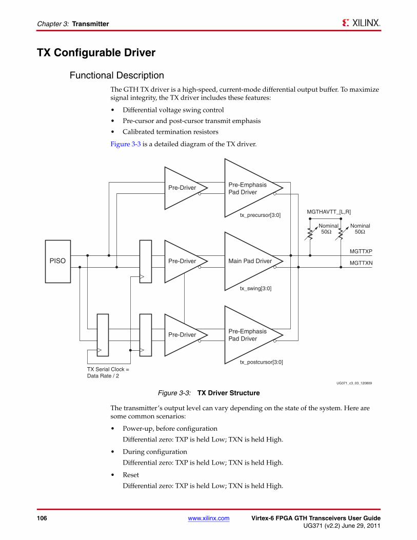
106 www.xilinx.com Virtex-6 FPGA GTH Transceivers User GuideUG371 (v2.2) June 29, 2011
Chapter 3: Transmitter
TX Configurable Driver
Functional DescriptionThe GTH TX driver is a high-speed, current-mode differential output buffer. To maximize signal integrity, the TX driver includes these features:
• Differential voltage swing control
• Pre-cursor and post-cursor transmit emphasis
• Calibrated termination resistors
Figure 3-3 is a detailed diagram of the TX driver.
The transmitter’s output level can vary depending on the state of the system. Here are some common scenarios:
• Power-up, before configuration
Differential zero: TXP is held Low; TXN is held High.
• During configuration
Differential zero: TXP is held Low; TXN is held High.
• Reset
Differential zero: TXP is held Low; TXN is held High.
X-Ref Target - Figure 3-3
Figure 3-3: TX Driver Structure
UG371_c3_03_120809
Pre-EmphasisPad Driver
Pre-EmphasisPad Driver
tx_precursor[3:0]MGTHAVTT_[L,R]
MGTTXP
MGTTXN
tx_swing[3:0]
tx_postcursor[3:0]TX Serial Clock =Data Rate / 2
Pre-Driver
Main Pad DriverPre-DriverPISO
Pre-Driver
50ΩNominal
50ΩNominal

Virtex-6 FPGA GTH Transceivers User Guide www.xilinx.com 107UG371 (v2.2) June 29, 2011
TX Configurable Driver
• Power down
Floating: TXP and TXN should float High to VTTX (assuming AC-coupled mode)
• Near-end PCS loopback and Near-end PMA loopback
TXP and TXN are transmitting live data
Ports and AttributesTable 3-14 defines the TX configurable driver ports.
Table 3-14: TX Configurable Driver Ports
Port Dir Clock Domain Description
TXDEEMPH0
TXDEEMPH1
TXDEEMPH2
TXDEEMPH3
In TXUSERCLKIN0
TXUSERCLKIN1
TXUSERCLKIN2
TXUSERCLKIN3
Reserved. Tie this input to 0.
TXMARGIN0[2:0]
TXMARGIN1[2:0]
TXMARGIN2[2:0]
TXMARGIN3[2:0]
In TXUSERCLKIN0
TXUSERCLKIN1
TXUSERCLKIN2
TXUSERCLKIN3
Reserved. Tie these inputs to 000.
TXN0
TXN1
TXN2
TXN3
TXP0
TXP1
TXP2
TXP3
Out(Pad)
TX Serial Clock TXP and TXN are the differential output pairs for each of the transmitters in the GTHE1_QUAD primitive. These ports represent pads. The location of these ports must be constrained and brought to the top level of the design.

108 www.xilinx.com Virtex-6 FPGA GTH Transceivers User GuideUG371 (v2.2) June 29, 2011
Chapter 3: Transmitter
Table 3-15 defines the TX configurable driver attributes.
Table 3-15: TX Configurable Driver Attributes
Attribute Type Description
TX_CFG0_LANE0
TX_CFG0_LANE1
TX_CFG0_LANE2
TX_CFG0_LANE3
16-bit Binary This attribute controls the differential voltage swing.
[15:14]: Reserved: 2’h0
[13]: Active-High TX lane power down (tx_chpd)
[12:7]: Reserved: 6’h00
[6:3]: TX output swing control and main tap/cursor control (tx_swing) Default: 4'h7
[2:0]: TX current bias fine swing control (tx_ibias)
tx_bias = 3'h5(1)
tx_swing(Binary)
TX_CFG0_LANE (Hex)
Voltage Swing (mVPPD)
0000 0x0005 450
0001 0x000D 500
0010 0x0015 550
0011 0x001D 600
0100 0x0025 650
0101 0x002D 700
0110 0x0035 750
0111 0x003D 800
1000 0x0045 850
1001 0x004D 900
1010 0x0055 950
1011 0x005D 1000
1100 0x0065 1050
1101 0x006D 1100
1110 0x0075 1150
1111 0x007D 1200
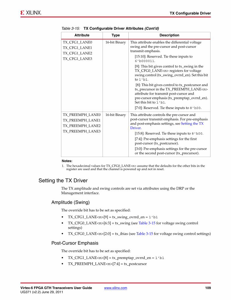
Virtex-6 FPGA GTH Transceivers User Guide www.xilinx.com 109UG371 (v2.2) June 29, 2011
TX Configurable Driver
Setting the TX DriverThe TX amplitude and swing controls are set via attributes using the DRP or the Management interface.
Amplitude (Swing)
The override bit has to be set as specified:
• TX_CFG1_LANE<n>[9] = tx_swing_ovrrd_en = 1'b1
• TX_CFG0_LANE<n>[6:3] = tx_swing (see Table 3-15 for voltage swing control settings)
• TX_CFG0_LANE<n>[2:0] = tx_ibias (see Table 3-15 for voltage swing control settings)
Post-Cursor Emphasis
The override bit has to be set as specified:
• TX_CFG1_LANE<n>[8] = tx_premptap_ovrrd_en = 1'b1
• TX_PREEMPH_LANE<n>[7:4] = tx_postcursor
TX_CFG1_LANE0
TX_CFG1_LANE1
TX_CFG1_LANE2
TX_CFG1_LANE3
16-bit Binary This attribute enables the differential voltage swing and the pre-cursor and post-cursor transmit emphasis.
[15:10]: Reserved. Tie these inputs to 6'b000011.
[9]: This bit gives control to tx_swing in the TX_CFG0_LANE<n> registers for voltage swing control (tx_swing_ovrrd_en). Set this bit to 1'b1.
[8]: This bit gives control to tx_postcursor and tx_precursor in the TX_PREEMPH_LANE<n> attribute for transmit post-cursor and pre-cursor emphasis (tx_premptap_ovrrd_en). Set this bit to 1'b1.
[7:0]: Reserved. Tie these inputs to 8'h00.
TX_PREEMPH_LANE0
TX_PREEMPH_LANE1
TX_PREEMPH_LANE2
TX_PREEMPH_LANE3
16-bit Binary This attribute controls the pre-cursor and post-cursor transmit emphasis. For pre-emphasis and post-emphasis settings, see Setting the TX Driver.
[15:8]: Reserved. Tie these inputs to 8'h00.
[7:4]: Pre-emphasis settings for the first post-cursor (tx_postcursor).
[3:0]: Pre-emphasis settings for the pre-cursor or the second post-cursor (tx_precursor).
Notes: 1. The hexadecimal values for TX_CFG0_LANE<n> assume that the defaults for the other bits in the
register are used and that the channel is powered up and not in reset.
Table 3-15: TX Configurable Driver Attributes (Cont’d)
Attribute Type Description
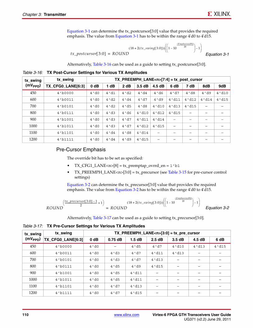
110 www.xilinx.com Virtex-6 FPGA GTH Transceivers User GuideUG371 (v2.2) June 29, 2011
Chapter 3: Transmitter
Equation 3-1 can determine the tx_postcursor[3:0] value that provides the required emphasis. The value from Equation 3-1 has to be within the range 4'd0 to 4'd15.
Equation 3-1
Alternatively, Table 3-16 can be used as a guide to setting tx_postcursor[3:0].
Pre-Cursor Emphasis
The override bit has to be set as specified:
• TX_CFG1_LANE<n>[8] = tx_premptap_ovrrd_en = 1'b1
• TX_PREEMPH_LANE<n>[3:0] = tx_precursor (see Table 3-15 for pre-cursor control settings)
Equation 3-2 can determine the tx_precursor[3:0] value that provides the required emphasis. The value from Equation 3-2 has to be within the range 4'd0 to 4'd15.
Equation 3-2
Alternatively, Table 3-17 can be used as a guide to setting tx_precursor[3:0].
tx_postcursor 3:0 ROUND18 2 tx_swing 3:0 + 1 10
- Emphasis dB 20
--------------------------------------------
–
1–
=
Table 3-16: TX Post-Cursor Settings for Various TX Amplitudes
tx_swing (mVPPD)
tx_swing TX_PREEMPH_LANE<n>[7:4] = tx_post_cursor
TX_CFG0_LANE[6:3] 0 dB 1 dB 2 dB 3.5 dB 4.5 dB 6 dB 7 dB 8dB 9dB
450 4'b0000 4'd0 4'd1 4'd2 4'd4 4'd6 4'd7 4'd8 4'd9 4'd10
600 4'b0011 4'd0 4'd2 4'd4 4'd7 4'd9 4'd11 4'd12 4'd14 4'd15
700 4'b0101 4'd0 4'd2 4'd5 4'd8 4'd10 4'd13 4'd15 – –
800 4'b0111 4'd0 4'd3 4'd6 4'd10 4'd12 4'd15 – – –
900 4'b1001 4'd0 4'd3 4'd7 4'd11 4'd14 – – – –
1000 4'b1011 4'd0 4'd3 4'd7 4'd12 4'd15 – – – –
1100 4'b1101 4'd0 4'd4 4'd8 4'd14 – – – – –
1200 4'b1111 4'd0 4'd4 4'd9 4'd15 – – – – –
ROUND
tx_precursor 3:0 1–2
---------------------------------------------------------- 1+
ROUND18 2 tx_swing 3:0 + 1 10
- Emphasis dB 20
--------------------------------------------
–
1–
=
Table 3-17: TX Pre-Cursor Settings for Various TX Amplitudes
tx_swing (mVPPD)
tx_swing TX_PREEMPH_LANE<n>[3:0] = tx_pre_cursor
TX_CFG0_LANE[6:3] 0 dB 0.75 dB 1.5 dB 2.5 dB 3.5 dB 4.5 dB 6 dB
450 4'b0000 4'd0 – 4'd5 4'd7 4'd10 4'd13 4'd15
600 4'b0011 4'd0 4'd3 4'd7 4'd11 4'd13 – –
700 4'b0101 4'd0 4'd3 4'd7 4'd13 – – –
800 4'b0111 4'd0 4'd5 4'd9 4'd15 – – –
900 4'b1001 4'd0 4'd5 4'd11 – – – –
1000 4'b1011 4'd0 4'd5 4'd11 – – – –
1100 4'b1101 4'd0 4'd7 4'd13 – – – –
1200 4'b1111 4'd0 4'd7 4'd15 – – – –

Virtex-6 FPGA GTH Transceivers User Guide www.xilinx.com 111UG371 (v2.2) June 29, 2011
Chapter 4
Receiver
This chapter describes how to configure and use each of the functional blocks inside the GTH receiver (RX). Each GTH transceiver in the GTH Quad includes an independent receiver, which consists of a PCS and a PMA.
The key elements within the GTH RX are:
• RX Analog Front End, page 112
• RX Equalization, page 113
• RX CDR, page 118
• RX Polarity Control, page 120
• RX Pattern Checker, page 122
• RX Raw Mode, page 127
• RX 10 Gigabit Ethernet 64B/66B Block, page 132
• RX 8B/10B Block, page 136
• FPGA RX Interface, page 140

112 www.xilinx.com Virtex-6 FPGA GTH Transceivers User GuideUG371 (v2.2) June 29, 2011
Chapter 4: Receiver
RX Analog Front EndThe RX analog front end (AFE) is a high-speed, current-mode, input differential buffer with calibrated termination resistors. Figure 4-1 shows the structure of the RX AFE.
Different conditions must be considered when configuring the RX AFE. Table 4-1 shows examples of those conditions.
X-Ref Target - Figure 4-1
Figure 4-1: Structure of the RX AFE
UG371_c4_02_091610
MGTHAVCCRX_[L,R]
FPGABoard
NominalVCM = 0.7V
NominalVCM = 0.7V
Nominal66 pF
GND
Nominal
50Ω
50Ω
Nominal
GND
~100 nF
~100 nF
Nominal
1KΩ
1KΩ
Nominal
MGTHAVCCRX_[L,R]
Table 4-1: RX AFE Board Interface Configurations
RX Configuration
Recom-mended
CommentsTransceiver Power Pins Connected to
Power
Transceiver GND Referenced with
Link Partner
RX Driven by Link Partner
Coupling (AC/DC)
Transceiver Configured via
Bitstream
RX Powered Down Via Attributes
– N – – – – N
Link partners should be GND referenced, otherwise the relative offsets can damage the FPGA.
– – – DC – – N Only AC coupling mode is supported
N Y Y AC – – Y
Y Y Y AC N N Y The receiver common mode becomes MGTHAVCCRX. The single-ended swing absolute value is limited by the maximum voltage value of the RXP/RXN signals specified in DS152, Virtex-6 FPGA Data Sheet: DC and Switching Characteristics.
Y Y Y AC
N (configuration ongoing and not complete)
N Y
Y Y Y AC Y Y Y
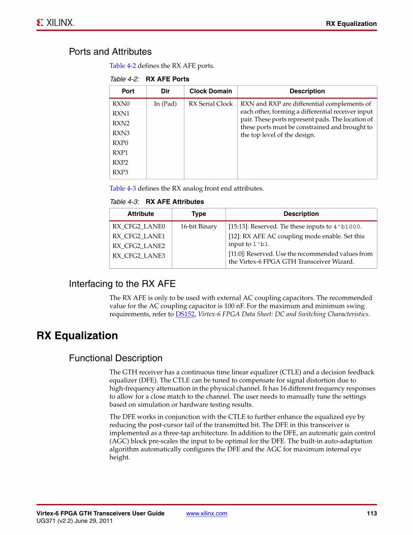
Virtex-6 FPGA GTH Transceivers User Guide www.xilinx.com 113UG371 (v2.2) June 29, 2011
RX Equalization
Ports and AttributesTable 4-2 defines the RX AFE ports.
Table 4-3 defines the RX analog front end attributes.
Interfacing to the RX AFEThe RX AFE is only to be used with external AC coupling capacitors. The recommended value for the AC coupling capacitor is 100 nF. For the maximum and minimum swing requirements, refer to DS152, Virtex-6 FPGA Data Sheet: DC and Switching Characteristics.
RX Equalization
Functional DescriptionThe GTH receiver has a continuous time linear equalizer (CTLE) and a decision feedback equalizer (DFE). The CTLE can be tuned to compensate for signal distortion due to high-frequency attenuation in the physical channel. It has 16 different frequency responses to allow for a close match to the channel. The user needs to manually tune the settings based on simulation or hardware testing results.
The DFE works in conjunction with the CTLE to further enhance the equalized eye by reducing the post-cursor tail of the transmitted bit. The DFE in this transceiver is implemented as a three-tap architecture. In addition to the DFE, an automatic gain control (AGC) block pre-scales the input to be optimal for the DFE. The built-in auto-adaptation algorithm automatically configures the DFE and the AGC for maximum internal eye height.
Table 4-2: RX AFE Ports
Port Dir Clock Domain Description
RXN0
RXN1
RXN2
RXN3
RXP0
RXP1
RXP2
RXP3
In (Pad) RX Serial Clock RXN and RXP are differential complements of each other, forming a differential receiver input pair. These ports represent pads. The location of these ports must be constrained and brought to the top level of the design.
Table 4-3: RX AFE Attributes
Attribute Type Description
RX_CFG2_LANE0
RX_CFG2_LANE1
RX_CFG2_LANE2
RX_CFG2_LANE3
16-bit Binary [15:13]: Reserved. Tie these inputs to 4'b1000.
[12]: RX AFE AC coupling mode enable. Set this input to 1'b1.
[11:0]: Reserved. Use the recommended values from the Virtex-6 FPGA GTH Transceiver Wizard.

114 www.xilinx.com Virtex-6 FPGA GTH Transceivers User GuideUG371 (v2.2) June 29, 2011
Chapter 4: Receiver
Figure 4-2 provides a top-level illustration of the AFE with the CTLE, DFE, and CDR.
Ports and AttributesTable 4-4 defines the RX equalization ports.
X-Ref Target - Figure 4-2
Figure 4-2: RX Equalization Block Diagram
UG371_c4_03_120809
DFE SIPO
DFE AdaptionLogic
CTLE
CDR
RX AFE
Table 4-4: RX Equalization Ports
Port Dir Clock Domain Description
DFETRAINCTRL0
DFETRAINCTRL1
DFETRAINCTRL2
DFETRAINCTRL3
In DCLK When the DFE is enabled, asserting this pin overrides completion of the DFE training.

Virtex-6 FPGA GTH Transceivers User Guide www.xilinx.com 115UG371 (v2.2) June 29, 2011
RX Equalization
Table 4-5 defines the RX equalization attributes.
Table 4-5: RX Equalization Attributes
Attribute Type Description
DFE_TRAIN_CTRL_LANE0
DFE_TRAIN_CTRL_LANE1
DFE_TRAIN_CTRL_LANE2
DFE_TRAIN_CTRL_LANE3
16-bit Hex This attribute controls the DFE.
[15]: 8B/10B mode and PRBS train_ok qualifier for the DFE. This bit qualifies train_ok signal from the 8B/10B and the RX PRBS blocks. This bit defaults to 1'b1 for modes that use 8B/10B encoding or PRBS.
[14]: Raw mode train_ok qualifier for the DFE. This bit qualifies the train_ok signal for Raw mode. This bit defaults to 1'b1 for modes that do not use 8B/10B or 64B/66B encoding or PRBS.
[13]: 64B/66B mode train_ok qualifier for the DFE. This bit qualifies the train_ok signal from the 64B/66B RX block. This bit defaults to 1'b1 for modes that use 64B/66B encoding.
[12:0]: DFE train limit. These bits contain the number (in 1K units) of consecutive error-free symbols that must be received before exiting DFE training mode. The setting on these bits varies per mode:
• 64B/66B (use 10GBASE-KR as an example): 13'h04C4
• 8B/10B: 13'h03D0• PRBS: 13'h04C4• Raw: If data encoding is similar to
64B/66B, use 13'h04C4. If data encoding is similar to 8B/10B, use 13'h03D0.
RX_AEQ_MON0_LANE0
RX_AEQ_MON0_LANE1
RX_AEQ_MON0_LANE2
RX_AEQ_MON0_LANE3
16-bit hex [3] DFETAP3 MONITOR SIGN BIT
[2:0] DFETAP3 MONITOR [3:1]
RX_AEQ_MON1_LANE0
RX_AEQ_MON1_LANE1
RX_AEQ_MON1_LANE2
RX_AEQ_MON1_LANE3
16-bit hex [15] DFETAP3 MONITOR [0]
[14] DFETAP2 MONITOR SIGN BIT
[13:10] DFETAP2 MONITOR [3:0]
[9:5] DFETAP1 MOINTOR [4:0]
[4:0] AGC MONITOR
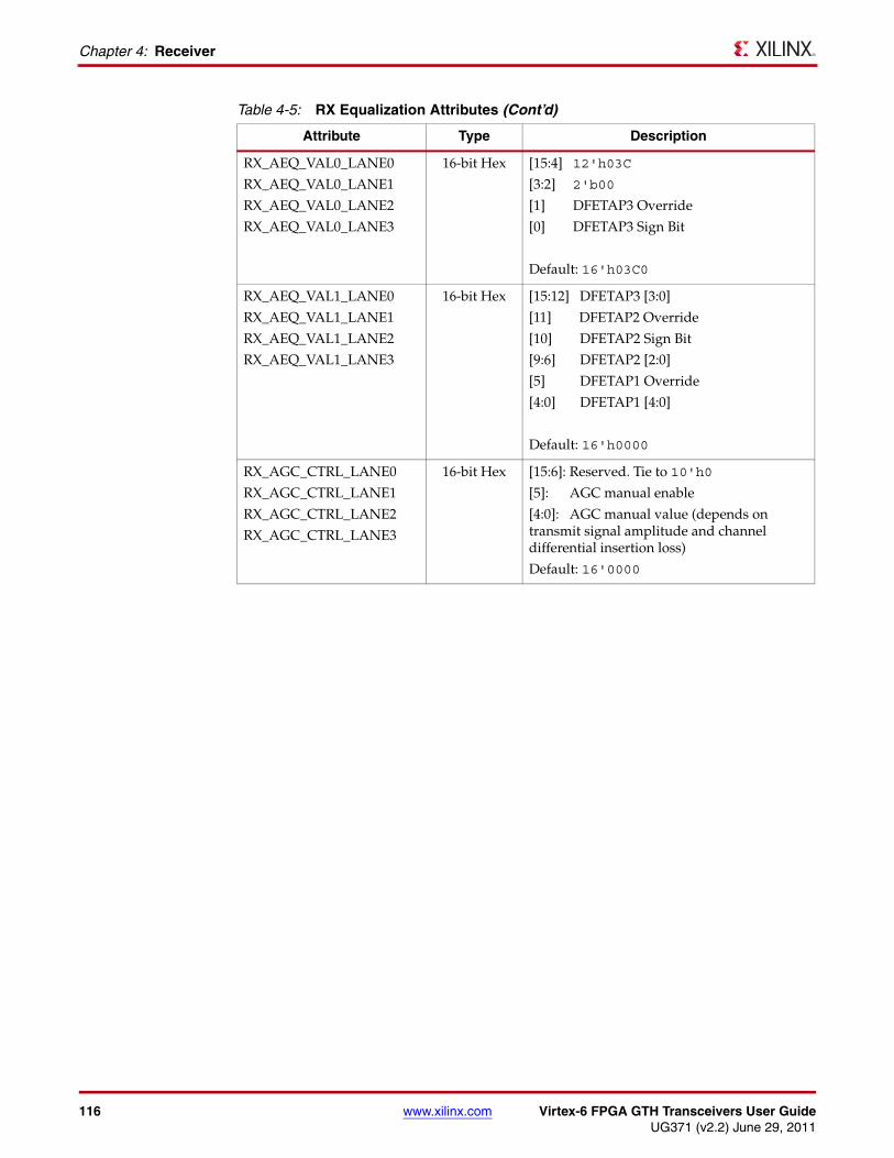
116 www.xilinx.com Virtex-6 FPGA GTH Transceivers User GuideUG371 (v2.2) June 29, 2011
Chapter 4: Receiver
RX_AEQ_VAL0_LANE0
RX_AEQ_VAL0_LANE1
RX_AEQ_VAL0_LANE2
RX_AEQ_VAL0_LANE3
16-bit Hex [15:4] 12'h03C
[3:2] 2'b00
[1] DFETAP3 Override
[0] DFETAP3 Sign Bit
Default: 16'h03C0
RX_AEQ_VAL1_LANE0
RX_AEQ_VAL1_LANE1
RX_AEQ_VAL1_LANE2
RX_AEQ_VAL1_LANE3
16-bit Hex [15:12] DFETAP3 [3:0]
[11] DFETAP2 Override
[10] DFETAP2 Sign Bit
[9:6] DFETAP2 [2:0]
[5] DFETAP1 Override
[4:0] DFETAP1 [4:0]
Default: 16'h0000
RX_AGC_CTRL_LANE0
RX_AGC_CTRL_LANE1
RX_AGC_CTRL_LANE2
RX_AGC_CTRL_LANE3
16-bit Hex [15:6]: Reserved. Tie to 10'h0
[5]: AGC manual enable
[4:0]: AGC manual value (depends on transmit signal amplitude and channel differential insertion loss)
Default: 16'0000
Table 4-5: RX Equalization Attributes (Cont’d)
Attribute Type Description

Virtex-6 FPGA GTH Transceivers User Guide www.xilinx.com 117UG371 (v2.2) June 29, 2011
RX Equalization
Use Mode: Channel Loss up to 8 dB with No TX EmphasisThis section describes how the AGC, DFE, and CTLE should be configured for channel differential insertion losses 8 dB with no TX Emphasis.
AGC
Set the AGC using the following guidelines.
RX_CTLE_CTRL_LANE0
RX_CTLE_CTRL_LANE1
RX_CTLE_CTRL_LANE2
RX_CTLE_CTRL_LANE3
16-bit Hex This attribute controls the RX CTLE peaking.
[15:8]: Reserved. Tie these inputs to 8'h00.
[7:4]: RX CTLE Peak Control. The peaking is mainly focused around 2.5 GHz.
[3:0]: Reserved. Tie these inputs to 4'hF.
Default: 16'h008F
Table 4-5: RX Equalization Attributes (Cont’d)
Attribute Type Description
dB - Nominal
0 0.15
1 0.36
2 0.74
3 0.96
4 1.98
5 2.19
6 2.71
7 2.88
8 4.15
9 4.32
A 4.64
B 4.79
C 5.20
D 5.34
E 5.54
F 5.67

118 www.xilinx.com Virtex-6 FPGA GTH Transceivers User GuideUG371 (v2.2) June 29, 2011
Chapter 4: Receiver
DFE
The DFE is auto-adapting but requires some training control parameters to be set. For modes that use the internal 8B/10B and PRBS blocks, DFE_TRAIN_CTRL_LANE<n>[15:13] = 100. For modes that use the internal 64B/66B blocks, DFE_TRAIN_CTRL_LANE<n>[15:13] = 001.
The DFE train limit needs to be set for both modes to determine the number of consecutive error-free multiple 1K symbols. Table 4-5 provides the guidelines for various datapath modes. Upon exit of DFE training, the DFE continues to adapt albeit much more slowly to track long term temperature and voltage variations.
For the Raw mode, DFE_TRAIN_CTRL_LANE<n>[15:13] = 010. The DFE train limit is ignored in this mode.
CTLE
The CTLE has static settings that must be set manually. The CTLE peaking is centered around 2 GHz to 2.5 GHz and is meant to compensate for the attenuation in the low- to mid-frequency band. The DFE compensates for the attenuation in the higher frequencies. RX_CTLE_CTRL_LANE0<n>[7:4] (decimal) = 3 + 1 code for every 0.5dB channel loss at Nyquist.
RX CDR
Functional DescriptionThe RX clock data recovery (CDR) circuit in each GTH transceiver extracts the recovered clock and data from an incoming data stream. Figure 4-3 illustrates the architecture of the CDR block. Clock paths are shown with dotted lines for clarity.
Table 4-6: AGC Settings
TX Launch Amplitude Vp-p,diff (mV) Value
>= 450 (1) [5] = 0
[4:0] = 5’b00000
(AGC in Auto)
Full Range [5] = 1 [4:0] = 5’b10000
(AGC in Manual Mode)
1. If acceptable BER is not achieved, use the Full Range setting.

Virtex-6 FPGA GTH Transceivers User Guide www.xilinx.com 119UG371 (v2.2) June 29, 2011
RX CDR
The GTH transceiver employs a phase rotator CDR architecture. Incoming data first goes through the RX equalization stages. The equalized data is then captured by an edge and a data sampler. The data captured by the data sampler is fed to the downstream RX blocks.
The CDR state machine uses the data from both the edge and data samplers to determine the phase of the incoming data stream and to control the phase interpolators (PIs). The phase for the edge sampler is locked to the transition region of the data stream while the phase of the data sampler is positioned in the middle of the data eye. Figure 4-4 shows the CDR sampler positions.
The shared Quad PLL provides a base clock to the phase interpolator. The phase interpolator in term produces fine, evenly spaced sampling phases to allow the CDR state machine to have fine phase control. The CDR state machine can track an incoming data stream with a frequency offset, usually no more than ±100 PPM, from the local PLL reference clock.
X-Ref Target - Figure 4-3
Figure 4-3: RX CDR Block Diagram
UG371_c4_04_120709
RXEQRXP/N
REFCLK
DFE
Demux
PI (E)
DataSampler
SharedQuad PLL
EdgeSampler
CDRFSM
Demux
PI (D)
RXDATA
RXRECCLK
GTH Lane
GTH Quad Shared Blocks
X-Ref Target - Figure 4-4
Figure 4-4: CDR Sampler Positions
UG371_c4_05_120709
E0 E1 E2
D0 D1

120 www.xilinx.com Virtex-6 FPGA GTH Transceivers User GuideUG371 (v2.2) June 29, 2011
Chapter 4: Receiver
Ports and AttributesThere are no ports in the CDR block.
Table 4-7 defines the RX CDR attributes.
Use Mode: General OperationUse the recommended values from the Virtex-6 FPGA GTH Transceiver Wizard.
RX Polarity Control
Functional DescriptionThe GTH RX can invert incoming data using the RX polarity control function. This function is useful in designs where the RXP and RXN signals can be accidentally connected in reverse.
Ports and AttributesTable 4-8 defines the RX polarity control ports..
Table 4-7: RX CDR Attributes
Attribute Type Description
RX_CDR_CTRL0_LANE0
RX_CDR_CTRL0_LANE1
RX_CDR_CTRL0_LANE2
RX_CDR_CTRL0_LANE3
16-bit Hex Reserved. Use the recommended values from the Virtex-6 FPGA GTH Transceiver Wizard.
RX_CDR_CTRL1_LANE0
RX_CDR_CTRL1_LANE1
RX_CDR_CTRL1_LANE2
RX_CDR_CTRL1_LANE3
16-bit Hex Reserved. Tie to 16'h4200.
RX_CDR_CTRL2_LANE0
RX_CDR_CTRL2_LANE1
RX_CDR_CTRL2_LANE2
RX_CDR_CTRL2_LANE3
16-bit Hex Reserved. Use the recommended values from the Virtex-6 FPGA GTH Transceiver Wizard.
RX_LOOP_CTRL_LANE0
RX_LOOP_CTRL_LANE1
RX_LOOP_CTRL_LANE2
RX_LOOP_CTRL_LANE3
16-bit Hex Reserved. Use the recommended values from the Virtex-6 FPGA GTH Transceiver Wizard.
Table 4-8: RX Polarity Control Ports
Port Dir Clock Domain Description
RXPOLARITY0
RXPOLARITY1
RXPOLARITY2
RXPOLARITY3
In RXUSERCLKIN0
RXUSERCLKIN1
RXUSERCLKIN2
RXUSERCLKIN3
The RX polarity port is used to invert the polarity of incoming data.
1: Invert polarity
0: Regular polarity

Virtex-6 FPGA GTH Transceivers User Guide www.xilinx.com 121UG371 (v2.2) June 29, 2011
RX Polarity Control
Table 4-9 defines the RX polarity control attributes..
Table 4-9: RX Polarity Control Attributes
Attribute Type Description
PCS_MISC_CFG_0_LANE0
PCS_MISC_CFG_0_LANE1
PCS_MISC_CFG_0_LANE2
PCS_MISC_CFG_0_LANE3
16-bit Hex This attribute sets the polarity and PRBS configuration.
[15:12]: Reserved. Use the recommended values from the Virtex-6 FPGA GTH Transceiver Wizard.
[11]: Invert TX polarity
[10]: RX polarity override enable
[9]: RX polarity override value
[8]: Reset the PRBS error counter when read
[7]: Revert bit order of parallel data to serializer/deserializer TX
[6]: Revert bit order of parallel data from serializer/deserializer RX
[5:0]: Reserved.
Tie to 6'h16 when TXRATE=2'b00
Tie to 6'h17 when TXRATE=2'b01
Tie to 6'h14 when TXRATE=2'b10
Tie to 6'h14 when TXRATE=2'b11

122 www.xilinx.com Virtex-6 FPGA GTH Transceivers User GuideUG371 (v2.2) June 29, 2011
Chapter 4: Receiver
Using RX Polarity ControlIf the polarity of RXP/RXN needs to be inverted, RXPOLARITY must be tied High. Alternatively, the DRP or management interface can be used to set PCS_MISC_CFG_0_LANE<n>[10:9] to 2'b11. The register is located in:
• DRP Address
• PCS_MISC_CFG_0_LANE0: 0x5001• PCS_MISC_CFG_0_LANE1: 0x5101• PCS_MISC_CFG_0_LANE2: 0x5201• PCS_MISC_CFG_0_LANE3: 0x5301
• Management Interface Address: 0x8001 with MMD Address 0x03
Use the Lane Address setting to specify which GTH lane to access.
RX Pattern Checker
Functional DescriptionThe GTH receiver contains a built-in pattern checker block. The checker supports the following PRBS patterns:
• PRBS7
• PRBS9
• PRBS11
• PRBS23
• PRBS31
In 64B/66B mode (for example, when the GTH transceiver is configured with the 10GBASE-R protocol), the checker is forced into PRBS31 mode when PRBS31 test pattern mode is enabled.
The PRBS checker module implements a 32-bit error counter and a 48-bit timer. The error counter and timer function as follows:
• The first read of any error counter/timer register latches both the error counter/timer in shadow flops.
• If the read was of an error counter and clear-on-read is on, both the timer and error counter are cleared.
• Reads of just the timer register (i.e., without first reading the error counter) do not clear the error count/timer, even if clear-on-read mode is on.
• Subsequent reads from error counter/timer addresses greater than the previous read address only read the shadow flops, do not read the actual state of the error counter/timer, and do not clear the error counter timer.
• Subsequent reads from error counter/timer addresses equal to or less than the read of the previous error counter/timer start the process over.
The error and sample counters saturate when they reach the maximum value.
In pattern check mode, data does not appear on RXDATA ports.
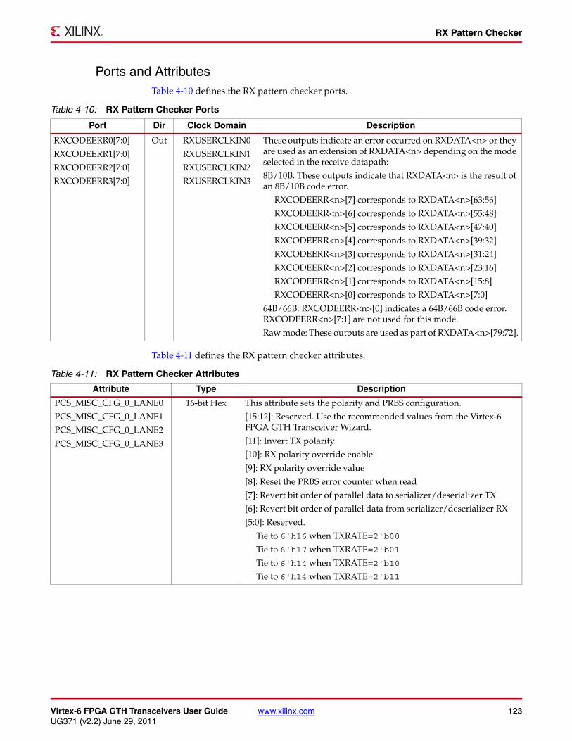
Virtex-6 FPGA GTH Transceivers User Guide www.xilinx.com 123UG371 (v2.2) June 29, 2011
RX Pattern Checker
Ports and AttributesTable 4-10 defines the RX pattern checker ports..
Table 4-11 defines the RX pattern checker attributes.
Table 4-10: RX Pattern Checker Ports
Port Dir Clock Domain Description
RXCODEERR0[7:0]
RXCODEERR1[7:0]
RXCODEERR2[7:0]
RXCODEERR3[7:0]
Out RXUSERCLKIN0
RXUSERCLKIN1
RXUSERCLKIN2
RXUSERCLKIN3
These outputs indicate an error occurred on RXDATA<n> or they are used as an extension of RXDATA<n> depending on the mode selected in the receive datapath:
8B/10B: These outputs indicate that RXDATA<n> is the result of an 8B/10B code error.
RXCODEERR<n>[7] corresponds to RXDATA<n>[63:56]
RXCODEERR<n>[6] corresponds to RXDATA<n>[55:48]
RXCODEERR<n>[5] corresponds to RXDATA<n>[47:40]
RXCODEERR<n>[4] corresponds to RXDATA<n>[39:32]
RXCODEERR<n>[3] corresponds to RXDATA<n>[31:24]
RXCODEERR<n>[2] corresponds to RXDATA<n>[23:16]
RXCODEERR<n>[1] corresponds to RXDATA<n>[15:8]
RXCODEERR<n>[0] corresponds to RXDATA<n>[7:0]
64B/66B: RXCODEERR<n>[0] indicates a 64B/66B code error. RXCODEERR<n>[7:1] are not used for this mode.
Raw mode: These outputs are used as part of RXDATA<n>[79:72].
Table 4-11: RX Pattern Checker Attributes
Attribute Type Description
PCS_MISC_CFG_0_LANE0
PCS_MISC_CFG_0_LANE1
PCS_MISC_CFG_0_LANE2
PCS_MISC_CFG_0_LANE3
16-bit Hex This attribute sets the polarity and PRBS configuration.
[15:12]: Reserved. Use the recommended values from the Virtex-6 FPGA GTH Transceiver Wizard.
[11]: Invert TX polarity
[10]: RX polarity override enable
[9]: RX polarity override value
[8]: Reset the PRBS error counter when read
[7]: Revert bit order of parallel data to serializer/deserializer TX
[6]: Revert bit order of parallel data from serializer/deserializer RX
[5:0]: Reserved.
Tie to 6'h16 when TXRATE=2'b00
Tie to 6'h17 when TXRATE=2'b01
Tie to 6'h14 when TXRATE=2'b10
Tie to 6'h14 when TXRATE=2'b11
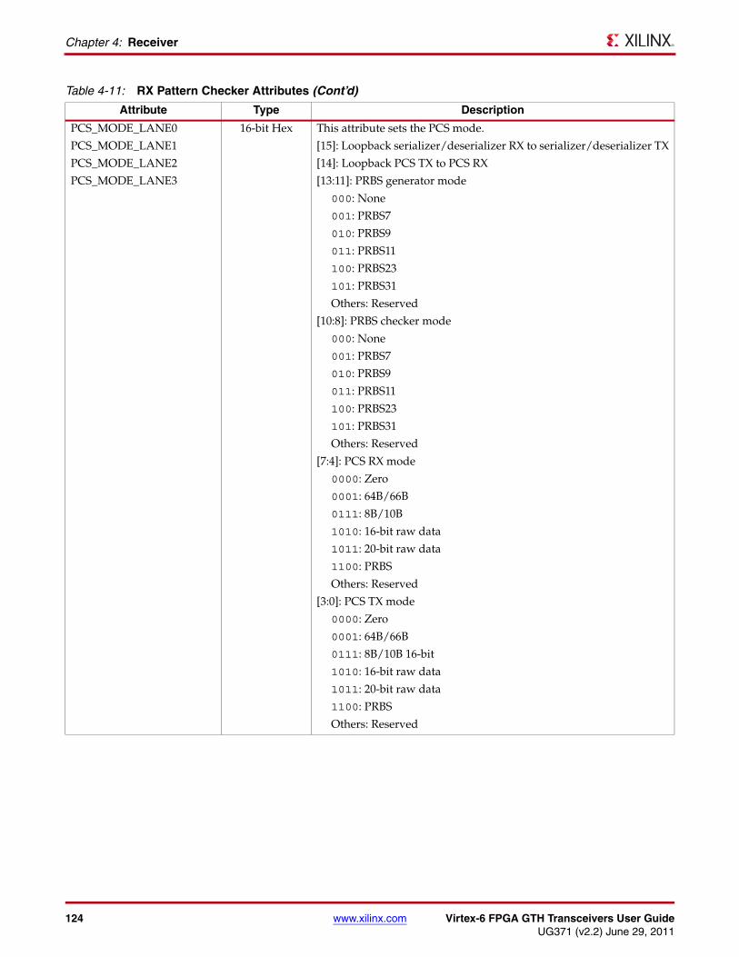
124 www.xilinx.com Virtex-6 FPGA GTH Transceivers User GuideUG371 (v2.2) June 29, 2011
Chapter 4: Receiver
PCS_MODE_LANE0
PCS_MODE_LANE1
PCS_MODE_LANE2
PCS_MODE_LANE3
16-bit Hex This attribute sets the PCS mode.
[15]: Loopback serializer/deserializer RX to serializer/deserializer TX
[14]: Loopback PCS TX to PCS RX
[13:11]: PRBS generator mode
000: None
001: PRBS7
010: PRBS9
011: PRBS11
100: PRBS23
101: PRBS31
Others: Reserved
[10:8]: PRBS checker mode
000: None
001: PRBS7
010: PRBS9
011: PRBS11
100: PRBS23
101: PRBS31
Others: Reserved
[7:4]: PCS RX mode
0000: Zero
0001: 64B/66B
0111: 8B/10B
1010: 16-bit raw data
1011: 20-bit raw data
1100: PRBS
Others: Reserved
[3:0]: PCS TX mode
0000: Zero
0001: 64B/66B
0111: 8B/10B 16-bit
1010: 16-bit raw data
1011: 20-bit raw data
1100: PRBS
Others: Reserved
Table 4-11: RX Pattern Checker Attributes (Cont’d)
Attribute Type Description

Virtex-6 FPGA GTH Transceivers User Guide www.xilinx.com 125UG371 (v2.2) June 29, 2011
RX Pattern Checker
PCS_RESET_LANE0
PCS_RESET_LANE1
PCS_RESET_LANE2
PCS_RESET_LANE3
16-bit Hex This attribute controls the datapath resets. These bits vary by mode:
64B/66B: 0xF3FE
8B/10B: 0xFC5B
Raw: 0xFF3B
PRBS: 0xFFCE
Default: 0xFFFF
[15:12]: Reserved
[11]: Reset 64B/66B receive
[10]: Reset 64B/66B transmit
[9]: Reset 8B/10B receive
[8]: Reset 8B/10B transmit
[7]: Reset RX FIFO
[6]: Reset RX raw shift pointer
[5]: Reset PRBS checker
[4]: Reset PRBS generator
[3]: Reserved
[2]: Reset TX FIFO
[1]: Reset RX loopback FIFO
[0]: Reserved
PCS_RESET_1_LANE0
PCS_RESET_1_LANE1
PCS_RESET_1_LANE2
PCS_RESET_1_LANE3
16-bit Hex [15:2]: Reserved. Use the recommended values from the Virtex-6 FPGA GTH Transceiver Wizard.
[1:0]: These bits control the datapath resets. They vary by mode:
64B/66B: 2'b10
8B/10B: 2'b00
Raw: 2'b00
PRBS: 2'b10
Default: 2'b11
PRBS_CFG_LANE0
PRBS_CFG_LANE1
PRBS_CFG_LANE2
PRBS_CFG_LANE3
16-bit Hex This attribute sets the PRBS data width.
[15:4]: Reserved. Use the recommended values from the Virtex-6 FPGA GTH Transceiver Wizard.
[3:2]: PRBS generate width
2'b11: 20b
2'b10: 16b
Others: Reserved
[1:0]: PRBS checker width
2'b11: 20b
2'b10: 16b
Others: Reserved
Table 4-11: RX Pattern Checker Attributes (Cont’d)
Attribute Type Description

126 www.xilinx.com Virtex-6 FPGA GTH Transceivers User GuideUG371 (v2.2) June 29, 2011
Chapter 4: Receiver
Table 4-12 defines the RX pattern checker registers.
Using RX Pattern CheckerFor the read-only registers, the DRP or management interface can be used for monitoring the PRBS error counter and the timer for PRBS testing.
• DRP Address
• PRBS_ERR_CNT0_LANE0: 0x5002
• PRBS_ERR_CNT0_LANE1: 0x5102
• PRBS_ERR_CNT0_LANE2: 0x5202
• PRBS_ERR_CNT0_LANE3: 0x5302
• PRBS_ERR_CNT1_LANE0: 0x5003
• PRBS_ERR_CNT1_LANE1: 0x5103
• PRBS_ERR_CNT1_LANE2: 0x5203
• PRBS_ERR_CNT1_LANE3: 0x5303
• PRBS_TIMER_0_LANE0: 0x5004
• PRBS_TIMER_0_LANE1: 0x5104
• PRBS_TIMER_0_LANE2: 0x5204
• PRBS_TIMER_0_LANE3: 0x5304
• PRBS_TIMER_1_LANE0: 0x5005
• PRBS_TIMER_1_LANE1: 0x5105
• PRBS_TIMER_1_LANE2: 0x5205
• PRBS_TIMER_1_LANE3: 0x5305
• PRBS_TIMER_2_LANE0: 0x5006
• PRBS_TIMER_2_LANE1: 0x5106
• PRBS_TIMER_2_LANE2: 0x5206
• PRBS_TIMER_2_LANE3: 0x5306
Table 4-12: RX Pattern Checker Registers (Read Only)
Register Name(1) Type Description
PRBS_ERR_CNT0_LANE<n> 16-bit Hex PRBS error counter [31:16]. Counter for PRBS or 8B/10B errors.
PRBS_ERR_CNT1_LANE<n> 16-bit Hex PRBS error counter [15:0]. Counter for PRBS or 8B/10B errors.
PRBS_TIMER_0_LANE<n> 16-bit Hex PRBS timer [47:32]. Timer for PRBS mode testing or monitoring.
PRBS_TIMER_1_LANE<n> 16-bit Hex PRBS timer [31:16]. Timer for PRBS mode testing or monitoring.
PRBS_TIMER_2_LANE<n> 16-bit Hex PRBS timer [15:0]. Timer for PRBS mode testing or monitoring.
Notes: 1. The DRP or the Management Interface must be used to access these registers.
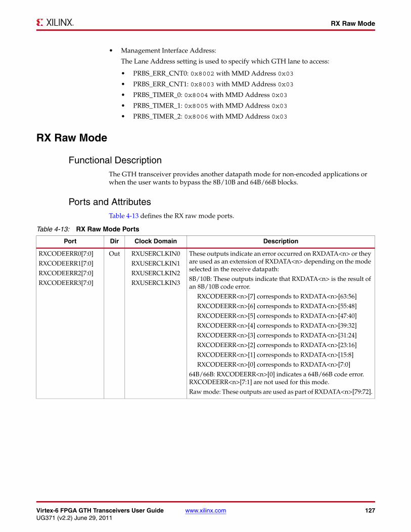
Virtex-6 FPGA GTH Transceivers User Guide www.xilinx.com 127UG371 (v2.2) June 29, 2011
RX Raw Mode
• Management Interface Address:
The Lane Address setting is used to specify which GTH lane to access:
• PRBS_ERR_CNT0: 0x8002 with MMD Address 0x03
• PRBS_ERR_CNT1: 0x8003 with MMD Address 0x03
• PRBS_TIMER_0: 0x8004 with MMD Address 0x03
• PRBS_TIMER_1: 0x8005 with MMD Address 0x03
• PRBS_TIMER_2: 0x8006 with MMD Address 0x03
RX Raw Mode
Functional DescriptionThe GTH transceiver provides another datapath mode for non-encoded applications or when the user wants to bypass the 8B/10B and 64B/66B blocks.
Ports and AttributesTable 4-13 defines the RX raw mode ports..
Table 4-13: RX Raw Mode Ports
Port Dir Clock Domain Description
RXCODEERR0[7:0]
RXCODEERR1[7:0]
RXCODEERR2[7:0]
RXCODEERR3[7:0]
Out RXUSERCLKIN0
RXUSERCLKIN1
RXUSERCLKIN2
RXUSERCLKIN3
These outputs indicate an error occurred on RXDATA<n> or they are used as an extension of RXDATA<n> depending on the mode selected in the receive datapath:
8B/10B: These outputs indicate that RXDATA<n> is the result of an 8B/10B code error.
RXCODEERR<n>[7] corresponds to RXDATA<n>[63:56]
RXCODEERR<n>[6] corresponds to RXDATA<n>[55:48]
RXCODEERR<n>[5] corresponds to RXDATA<n>[47:40]
RXCODEERR<n>[4] corresponds to RXDATA<n>[39:32]
RXCODEERR<n>[3] corresponds to RXDATA<n>[31:24]
RXCODEERR<n>[2] corresponds to RXDATA<n>[23:16]
RXCODEERR<n>[1] corresponds to RXDATA<n>[15:8]
RXCODEERR<n>[0] corresponds to RXDATA<n>[7:0]
64B/66B: RXCODEERR<n>[0] indicates a 64B/66B code error. RXCODEERR<n>[7:1] are not used for this mode.
Raw mode: These outputs are used as part of RXDATA<n>[79:72].
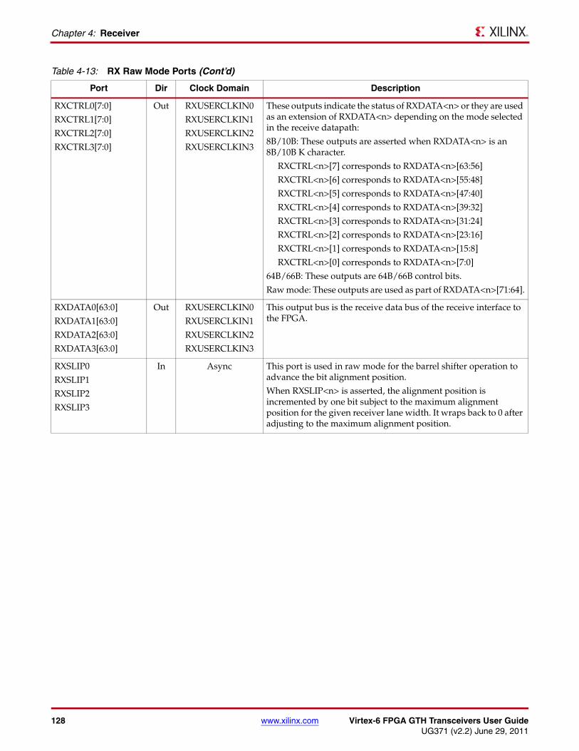
128 www.xilinx.com Virtex-6 FPGA GTH Transceivers User GuideUG371 (v2.2) June 29, 2011
Chapter 4: Receiver
RXCTRL0[7:0]
RXCTRL1[7:0]
RXCTRL2[7:0]
RXCTRL3[7:0]
Out RXUSERCLKIN0
RXUSERCLKIN1
RXUSERCLKIN2
RXUSERCLKIN3
These outputs indicate the status of RXDATA<n> or they are used as an extension of RXDATA<n> depending on the mode selected in the receive datapath:
8B/10B: These outputs are asserted when RXDATA<n> is an 8B/10B K character.
RXCTRL<n>[7] corresponds to RXDATA<n>[63:56]
RXCTRL<n>[6] corresponds to RXDATA<n>[55:48]
RXCTRL<n>[5] corresponds to RXDATA<n>[47:40]
RXCTRL<n>[4] corresponds to RXDATA<n>[39:32]
RXCTRL<n>[3] corresponds to RXDATA<n>[31:24]
RXCTRL<n>[2] corresponds to RXDATA<n>[23:16]
RXCTRL<n>[1] corresponds to RXDATA<n>[15:8]
RXCTRL<n>[0] corresponds to RXDATA<n>[7:0]
64B/66B: These outputs are 64B/66B control bits.
Raw mode: These outputs are used as part of RXDATA<n>[71:64].
RXDATA0[63:0]
RXDATA1[63:0]
RXDATA2[63:0]
RXDATA3[63:0]
Out RXUSERCLKIN0
RXUSERCLKIN1
RXUSERCLKIN2
RXUSERCLKIN3
This output bus is the receive data bus of the receive interface to the FPGA.
RXSLIP0
RXSLIP1
RXSLIP2
RXSLIP3
In Async This port is used in raw mode for the barrel shifter operation to advance the bit alignment position.
When RXSLIP<n> is asserted, the alignment position is incremented by one bit subject to the maximum alignment position for the given receiver lane width. It wraps back to 0 after adjusting to the maximum alignment position.
Table 4-13: RX Raw Mode Ports (Cont’d)
Port Dir Clock Domain Description
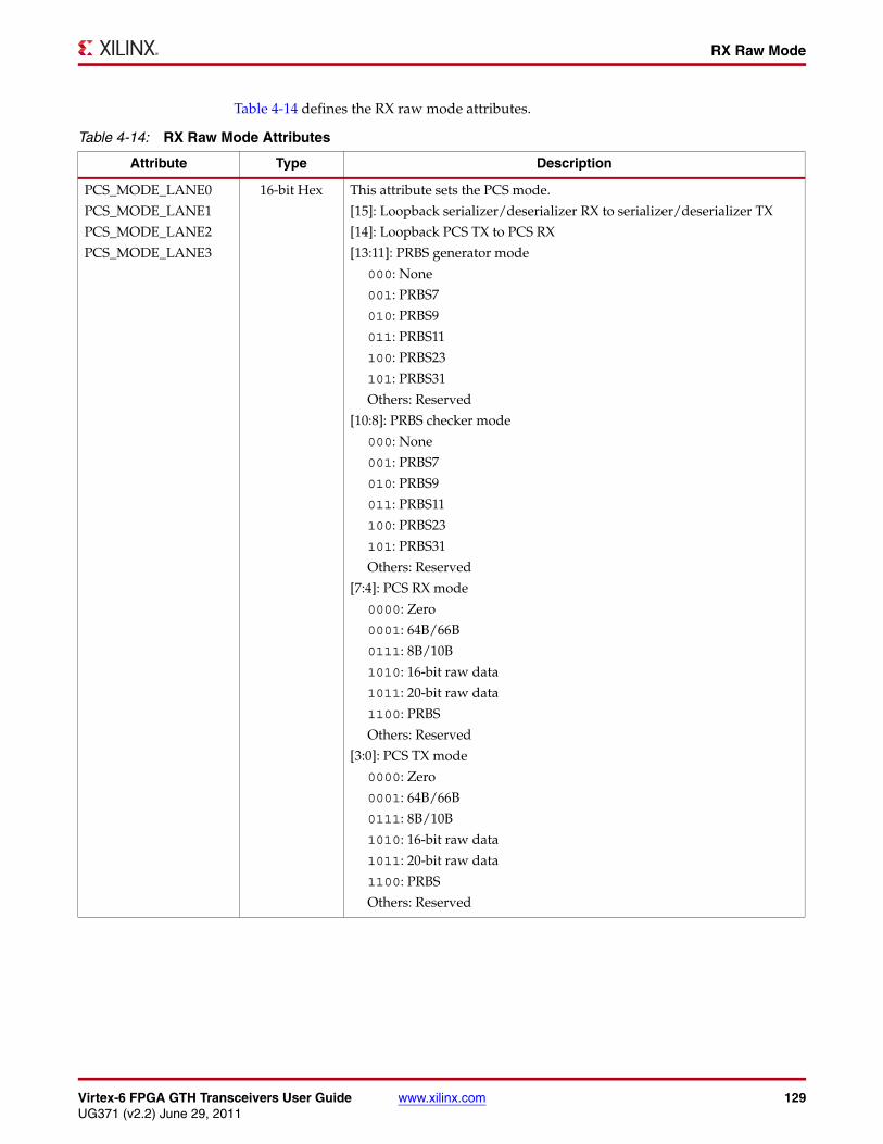
Virtex-6 FPGA GTH Transceivers User Guide www.xilinx.com 129UG371 (v2.2) June 29, 2011
RX Raw Mode
Table 4-14 defines the RX raw mode attributes.
Table 4-14: RX Raw Mode Attributes
Attribute Type Description
PCS_MODE_LANE0
PCS_MODE_LANE1
PCS_MODE_LANE2
PCS_MODE_LANE3
16-bit Hex This attribute sets the PCS mode.
[15]: Loopback serializer/deserializer RX to serializer/deserializer TX
[14]: Loopback PCS TX to PCS RX
[13:11]: PRBS generator mode
000: None
001: PRBS7
010: PRBS9
011: PRBS11
100: PRBS23
101: PRBS31
Others: Reserved
[10:8]: PRBS checker mode
000: None
001: PRBS7
010: PRBS9
011: PRBS11
100: PRBS23
101: PRBS31
Others: Reserved
[7:4]: PCS RX mode
0000: Zero
0001: 64B/66B
0111: 8B/10B
1010: 16-bit raw data
1011: 20-bit raw data
1100: PRBS
Others: Reserved
[3:0]: PCS TX mode
0000: Zero
0001: 64B/66B
0111: 8B/10B
1010: 16-bit raw data
1011: 20-bit raw data
1100: PRBS
Others: Reserved

130 www.xilinx.com Virtex-6 FPGA GTH Transceivers User GuideUG371 (v2.2) June 29, 2011
Chapter 4: Receiver
PCS_RESET_LANE0
PCS_RESET_LANE1
PCS_RESET_LANE2
PCS_RESET_LANE3
16-bit Hex This attribute controls the datapath resets. These bits vary by mode:
64B/66B: 0xF3FE
8B/10B: 0xFC5B
Raw: 0xFF3B
PRBS: 0xFFCE
Default: 0xFFFF
[15:12]: Reserved
[11]: Reset 64B/66B receive
[10]: Reset 64B/66B transmit
[9]: Reset 8B/10B receive
[8]: Reset 8B/10B transmit
[7]: Reset RX FIFO
[6]: Reset RX raw shift pointer
[5]: Reset PRBS checker
[4]: Reset PRBS generator
[3]: Reserved
[2]: Reset TX FIFO
[1]: Reset RX loopback FIFO
[0]: Reserved
PCS_RESET_1_LANE0
PCS_RESET_1_LANE1
PCS_RESET_1_LANE2
PCS_RESET_1_LANE3
16-bit Hex [15:2]: Reserved. Use the recommended values from theVirtex-6 FPGA GTH Transceiver Wizard.
[1:0]: These bits control the datapath resets. They vary by mode:
64B/66B: 2'b10
8B/10B: 2'b00
Raw: 2'b00
PRBS: 2'b10
Default: 2'b11
RX_FABRIC_WIDTH0
RX_FABRIC_WIDTH1
RX_FABRIC_WIDTH2
RX_FABRIC_WIDTH3
Integer This attribute sets the mapping of the internal data width (PCS) to the external data width (fabric) for the receiver. Valid settings are:
“16” (DRP value 3'b000): PCS to Fabric 1:1
“20” (DRP value 3'b000): PCS to Fabric 1:1
“32” (DRP value 3'b011): PCS to Fabric 1:2 32 bits
“40” (DRP value 3'b101): PCS to Fabric 1:2 40 bits
“64” (DRP value 3'b010): PCS to Fabric 1:4 64 bits
“80” (DRP value 3'b110): PCS to Fabric 1:4 80 bits
“6466” (DRP value 3'b111): 64B/66B mode
Table 4-14: RX Raw Mode Attributes (Cont’d)
Attribute Type Description

Virtex-6 FPGA GTH Transceivers User Guide www.xilinx.com 131UG371 (v2.2) June 29, 2011
RX Raw Mode
Table 4-15 defines the RX raw mode read-only registers.
Enabling Raw ModeFollow these steps to enable the raw mode in the GTH receiver:
1. If the receive fabric data width is configured to 16 bits, 32 bits, or 64 bits:
a. Set PCS_MODE_LANE<n>[7:4] to 4’b1010.
b. Set PCS_RESET_LANE<n> to 0xFF3B.
c. Set PCS_RESET_1_LANE<n>[1:0] to 2’b00.
d. Set RX_FABRIC_WIDTH<n> to “16”, “32”, or “64.”
2. If the receive fabric data width is configured to 20 bits, 40 bits, or 80 bits:
a. Set PCS_MODE_LANE<n>[7:4] to 4'b1011.
b. Set PCS_RESET_LANE<n> to 0xFF3B.
c. Set PCS_RESET_1_LANE<n>[1:0] to 2’b00.
d. Set RX_FABRIC_WIDTH<n> to “20”, “40”, or “80.”
Using the Barrel ShifterThe raw data mode provides control of the raw bit alignment position to the user. The user must drive RXSLIP port High to advance the bit alignment position. The bit alignment position starts at 0 upon reset and increments by one bit on every positive edge of RXSLIP.
The bit alignment position of the barrel shifter can be monitored through either the DRP interface or the management interface by accessing the RAW_SHIFT_MON_LANE<n>[4:0] register:
• DRP Address
• RAW_SHIFT_MON_LANE0: 0x500E
• RAW_SHIFT_MON_LANE1: 0x510E
• RAW_SHIFT_MON_LANE2: 0x520E
• RAW_SHIFT_MON_LANE3: 0x530E
• Management Interface Address: 0x800E with MMD Address 0x03
Use the Lane Address setting to specify which GTH lane to access.
Table 4-15: RX Raw Mode Read-only Registers
Read-only Registers Type Description
RAW_SHIFT_MON_LANE0
RAW_SHIFT_MON_LANE1
RAW_SHIFT_MON_LANE2
RAW_SHIFT_MON_LANE3
16-bit Hex This register is used for the barrel shifter from the raw data mode.
[15:5]: Reserved.
[4:0]: Bit position of the LSB of RX data in the serial-to-parallel data stream.

132 www.xilinx.com Virtex-6 FPGA GTH Transceivers User GuideUG371 (v2.2) June 29, 2011
Chapter 4: Receiver
RX 10 Gigabit Ethernet 64B/66B Block
Functional DescriptionThe GTH transceiver implements the 64B/66B block based on IEEE 802.3-2008 Clause 49, “Physical Sublayer (PCS) for 64B/66B, type 10GBASE-R.” The RX 10 Gb Ethernet 64B/66B block includes the block synchronization, the gearbox, and the descrambler.
Ports and AttributesTable 4-16 defines the RX 10 Gb Ethernet 64B/66B block ports.
Table 4-16: RX 10 Gb Ethernet 64B/66B Block Ports
Port Dir Clock Domain Description
RXCODEERR0[7:0]
RXCODEERR1[7:0]
RXCODEERR2[7:0]
RXCODEERR3[7:0]
Out RXUSERCLKIN0
RXUSERCLKIN1
RXUSERCLKIN2
RXUSERCLKIN3
These outputs indicate an error occurred on RXDATA<n> or they are used as an extension of RXDATA<n> depending on the mode selected in the receive datapath:
8B/10B: These outputs indicate that RXDATA<n> is the result of an 8B/10B code error.
RXCODEERR<n>[7] corresponds to RXDATA<n>[63:56]
RXCODEERR<n>[6] corresponds to RXDATA<n>[55:48]
RXCODEERR<n>[5] corresponds to RXDATA<n>[47:40]
RXCODEERR<n>[4] corresponds to RXDATA<n>[39:32]
RXCODEERR<n>[3] corresponds to RXDATA<n>[31:24]
RXCODEERR<n>[2] corresponds to RXDATA<n>[23:16]
RXCODEERR<n>[1] corresponds to RXDATA<n>[15:8]
RXCODEERR<n>[0] corresponds to RXDATA<n>[7:0]
64B/66B: RXCODEERR<n>[0] indicates a 64B/66B code error. RXCODEERR<n>[7:1] are not used for this mode.
Raw mode: These outputs are used as part of RXDATA<n>[79:72].

Virtex-6 FPGA GTH Transceivers User Guide www.xilinx.com 133UG371 (v2.2) June 29, 2011
RX 10 Gigabit Ethernet 64B/66B Block
RXCTRL0[7:0]
RXCTRL1[7:0]
RXCTRL2[7:0]
RXCTRL3[7:0]
Out RXUSERCLKIN0
RXUSERCLKIN1
RXUSERCLKIN2
RXUSERCLKIN3
These outputs indicate the status of RXDATA<n> or they are used as an extension of RXDATA<n> depending on the mode selected in the receive datapath:
8B/10B: These outputs are asserted when RXDATA<n> is an 8B/10B K character.
RXCTRL<n>[7] corresponds to RXDATA<n>[63:56]
RXCTRL<n>[6] corresponds to RXDATA<n>[55:48]
RXCTRL<n>[5] corresponds to RXDATA<n>[47:40]
RXCTRL<n>[4] corresponds to RXDATA<n>[39:32]
RXCTRL<n>[3] corresponds to RXDATA<n>[31:24]
RXCTRL<n>[2] corresponds to RXDATA<n>[23:16]
RXCTRL<n>[1] corresponds to RXDATA<n>[15:8]
RXCTRL<n>[0] corresponds to RXDATA<n>[7:0]
64B/66B: These outputs are 64B/66B control bits.
Raw mode: These outputs are used as part of RXDATA<n>[71:64].
RXDATA0[63:0]
RXDATA1[63:0]
RXDATA2[63:0]
RXDATA3[63:0]
Out RXUSERCLKIN0
RXUSERCLKIN1
RXUSERCLKIN2
RXUSERCLKIN3
This output bus is the receive data bus of the receive interface to the FPGA.
Table 4-16: RX 10 Gb Ethernet 64B/66B Block Ports (Cont’d)
Port Dir Clock Domain Description

134 www.xilinx.com Virtex-6 FPGA GTH Transceivers User GuideUG371 (v2.2) June 29, 2011
Chapter 4: Receiver
Table 4-17 defines the RX 10 Gb Ethernet 64B/66B block attributes.
Table 4-17: RX 10 Gb Ethernet 64B/66B Block Attributes
Attribute Type Description
PCS_MODE_LANE0
PCS_MODE_LANE1
PCS_MODE_LANE2
PCS_MODE_LANE3
16-bit Hex This attribute sets PCS mode.
[15]: Loopback serializer/deserializer RX to serializer/deserializer TX
[14]: Loopback PCS TX to PCS RX
[13:11]: PRBS generator mode
000: None
001: PRBS7
010: PRBS9
011: PRBS11
100: PRBS23
101: PRBS31
Others: Reserved
[10:8]: PRBS checker mode
000: None
001: PRBS7
010: PRBS9
011: PRBS11
100: PRBS23
101: PRBS31
Others: Reserved
[7:4]: PCS RX mode
0000: Zero
0001: 64B/66B
0111: 8B/10B
1010: 16-bit raw data
1011: 20-bit raw data
1100: PRBS
Others: Reserved
[3:0]: PCS TX mode
0000: Zero
0001: 64B/66B
0111: 8B/10B
1010: 16-bit raw data
1011: 20-bit raw data
1100: PRBS
Others: Reserved

Virtex-6 FPGA GTH Transceivers User Guide www.xilinx.com 135UG371 (v2.2) June 29, 2011
RX 10 Gigabit Ethernet 64B/66B Block
PCS_RESET_LANE0
PCS_RESET_LANE1
PCS_RESET_LANE2
PCS_RESET_LANE3
16-bit Hex This attribute controls the datapath resets. These bits vary by mode:
64B/66B: 0xF3FE
8B/10B: 0xFC5B
Raw: 0xFF3B
PRBS: 0xFFCE
Default: 0xFFFF
[15:12]: Reserved
[11]: Reset 64B/66B receive
[10]: Reset 64B/66B transmit
[9]: Reset 8B/10B receive
[8]: Reset 8B/10B transmit
[7]: Reset RX FIFO
[6]: Reset RX raw shift pointer
[5]: Reset PRBS checker
[4]: Reset PRBS generator
[3]: Reserved
[2]: Reset TX FIFO
[1]: Reset RX loopback FIFO
[0]: Reserved
PCS_RESET_1_LANE0
PCS_RESET_1_LANE1
PCS_RESET_1_LANE2
PCS_RESET_1_LANE3
16-bit Hex [15:2]: Reserved. Use the recommended values from the Virtex-6 FPGA GTH Transceiver Wizard.
[1:0]: These bits control the datapath resets. They vary by mode:
64B/66B: 2'b10
8B/10B: 2'b00
Raw: 2'b00
PRBS: 2'b10
Default: 2'b11
RX_FABRIC_WIDTH0
RX_FABRIC_WIDTH1
RX_FABRIC_WIDTH2
RX_FABRIC_WIDTH3
Integer This attribute sets the mapping of the internal data width (PCS) to the external data width (fabric) for the receiver. Valid settings are:
“16” (DRP value 3'b000): PCS to Fabric 1:1
“20” (DRP value 3'b000): PCS to Fabric 1:1
“32” (DRP value 3'b011): PCS to Fabric 1:2 32 bits
“40” (DRP value 3'b101): PCS to Fabric 1:2 40 bits
“64” (DRP value 3'b010): PCS to Fabric 1:4 64 bits
“80” (DRP value 3'b110): PCS to Fabric 1:4 80 bits
“6466” (DRP value 3'b111): 64B/66B mode
Table 4-17: RX 10 Gb Ethernet 64B/66B Block Attributes (Cont’d)
Attribute Type Description
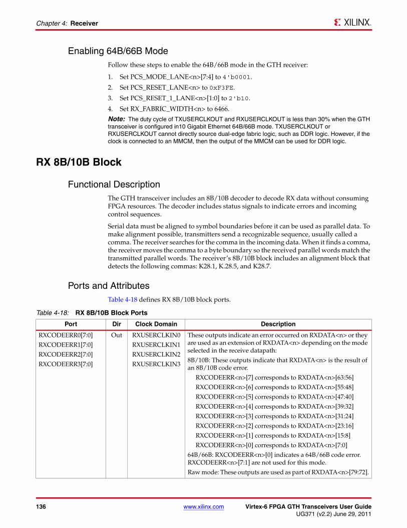
136 www.xilinx.com Virtex-6 FPGA GTH Transceivers User GuideUG371 (v2.2) June 29, 2011
Chapter 4: Receiver
Enabling 64B/66B ModeFollow these steps to enable the 64B/66B mode in the GTH receiver:
1. Set PCS_MODE_LANE<n>[7:4] to 4'b0001.
2. Set PCS_RESET_LANE<n> to 0xF3FE.
3. Set PCS_RESET_1_LANE<n>[1:0] to 2'b10.
4. Set RX_FABRIC_WIDTH<n> to 6466.
Note: The duty cycle of TXUSERCLKOUT and RXUSERCLKOUT is less than 30% when the GTH transceiver is configured in10 Gigabit Ethernet 64B/66B mode. TXUSERCLKOUT or RXUSERCLKOUT cannot directly source dual-edge fabric logic, such as DDR logic. However, if the clock is connected to an MMCM, then the output of the MMCM can be used for DDR logic.
RX 8B/10B Block
Functional DescriptionThe GTH transceiver includes an 8B/10B decoder to decode RX data without consuming FPGA resources. The decoder includes status signals to indicate errors and incoming control sequences.
Serial data must be aligned to symbol boundaries before it can be used as parallel data. To make alignment possible, transmitters send a recognizable sequence, usually called a comma. The receiver searches for the comma in the incoming data. When it finds a comma, the receiver moves the comma to a byte boundary so the received parallel words match the transmitted parallel words. The receiver’s 8B/10B block includes an alignment block that detects the following commas: K28.1, K.28.5, and K28.7.
Ports and AttributesTable 4-18 defines RX 8B/10B block ports..
Table 4-18: RX 8B/10B Block Ports
Port Dir Clock Domain Description
RXCODEERR0[7:0]
RXCODEERR1[7:0]
RXCODEERR2[7:0]
RXCODEERR3[7:0]
Out RXUSERCLKIN0
RXUSERCLKIN1
RXUSERCLKIN2
RXUSERCLKIN3
These outputs indicate an error occurred on RXDATA<n> or they are used as an extension of RXDATA<n> depending on the mode selected in the receive datapath:
8B/10B: These outputs indicate that RXDATA<n> is the result of an 8B/10B code error.
RXCODEERR<n>[7] corresponds to RXDATA<n>[63:56]
RXCODEERR<n>[6] corresponds to RXDATA<n>[55:48]
RXCODEERR<n>[5] corresponds to RXDATA<n>[47:40]
RXCODEERR<n>[4] corresponds to RXDATA<n>[39:32]
RXCODEERR<n>[3] corresponds to RXDATA<n>[31:24]
RXCODEERR<n>[2] corresponds to RXDATA<n>[23:16]
RXCODEERR<n>[1] corresponds to RXDATA<n>[15:8]
RXCODEERR<n>[0] corresponds to RXDATA<n>[7:0]
64B/66B: RXCODEERR<n>[0] indicates a 64B/66B code error. RXCODEERR<n>[7:1] are not used for this mode.
Raw mode: These outputs are used as part of RXDATA<n>[79:72].

Virtex-6 FPGA GTH Transceivers User Guide www.xilinx.com 137UG371 (v2.2) June 29, 2011
RX 8B/10B Block
RXCTRL0[7:0]
RXCTRL1[7:0]
RXCTRL2[7:0]
RXCTRL3[7:0]
Out RXUSERCLKIN0
RXUSERCLKIN1
RXUSERCLKIN2
RXUSERCLKIN3
These outputs indicate the status of RXDATA<n> or they are used as an extension of RXDATA<n> depending on the mode selected in the receive datapath:
8B/10B: These outputs are asserted when RXDATA<n> is an 8B/10B K character.
RXCTRL<n>[7] corresponds to RXDATA<n>[63:56]
RXCTRL<n>[6] corresponds to RXDATA<n>[55:48]
RXCTRL<n>[5] corresponds to RXDATA<n>[47:40]
RXCTRL<n>[4] corresponds to RXDATA<n>[39:32]
RXCTRL<n>[3] corresponds to RXDATA<n>[31:24]
RXCTRL<n>[2] corresponds to RXDATA<n>[23:16]
RXCTRL<n>[1] corresponds to RXDATA<n>[15:8]
RXCTRL<n>[0] corresponds to RXDATA<n>[7:0]
64B/66B: These outputs are 64B/66B control bits.
Raw mode: These outputs are used as part of RXDATA<n>[71:64].
RXDATA0[63:0]
RXDATA1[63:0]
RXDATA2[63:0]
RXDATA3[63:0]
Out RXUSERCLKIN0
RXUSERCLKIN1
RXUSERCLKIN2
RXUSERCLKIN3
This output bus is the receive data bus of the receive interface to the FPGA.
RXDISPERR0[7:0]
RXDISPERR1[7:0]
RXDISPERR2[7:0]
RXDISPERR3[7:0]
Out RXUSERCLKIN0
RXUSERCLKIN1
RXUSERCLKIN2
RXUSERCLKIN3
Used only for 8B/10B mode. These outputs indicate a disparity error occurred on RXDATA<n>.
RXDISPERR<n>[7] corresponds to RXDATA<n>[63:56]
RXDISPERR<n>[6] corresponds to RXDATA<n>[55:48]
RXDISPERR<n>[5] corresponds to RXDATA<n>[47:40]
RXDISPERR<n>[4] corresponds to RXDATA<n>[39:32]
RXDISPERR<n>[3] corresponds to RXDATA<n>[31:24]
RXDISPERR<n>[2] corresponds to RXDATA<n>[23:16]
RXDISPERR<n>[1] corresponds to RXDATA<n>[15:8]
RXDISPERR<n>[0] corresponds to RXDATA<n>[7:0]
RXENCOMMADET0
RXENCOMMADET1
RXENCOMMADET2
RXENCOMMADET3
In RXUSERCLKIN0
RXUSERCLKIN1
RXUSERCLKIN2
RXUSERCLKIN3
This input activates the comma detection and alignment circuit for 8B/10B mode.
RXVALID0[7:0]
RXVALID1[7:0]
RXVALID2[7:0]
RXVALID3[7:0]
Out RXUSERCLKIN0
RXUSERCLKIN1
RXUSERCLKIN2
RXUSERCLKIN3
These status outputs indicate which bytes are valid used in 8B/10B mode only.
RXVALID<n>[7] corresponds to RXDATA<n>[63:56]
RXVALID<n>[6] corresponds to RXDATA<n>[55:48]
RXVALID<n>[5] corresponds to RXDATA<n>[47:40]
RXVALID<n>[4] corresponds to RXDATA<n>[39:32]
RXVALID<n>[3] corresponds to RXDATA<n>[31:24]
RXVALID<n>[2] corresponds to RXDATA<n>[23:16]
RXVALID<n>[1] corresponds to RXDATA<n>[15:8]
RXVALID<n>[0] corresponds to RXDATA<n>[7:0]
Table 4-18: RX 8B/10B Block Ports (Cont’d)
Port Dir Clock Domain Description
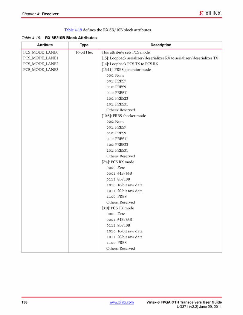
138 www.xilinx.com Virtex-6 FPGA GTH Transceivers User GuideUG371 (v2.2) June 29, 2011
Chapter 4: Receiver
Table 4-19 defines the RX 8B/10B block attributes..
Table 4-19: RX 8B/10B Block Attributes
Attribute Type Description
PCS_MODE_LANE0
PCS_MODE_LANE1
PCS_MODE_LANE2
PCS_MODE_LANE3
16-bit Hex This attribute sets PCS mode.
[15]: Loopback serializer/deserializer RX to serializer/deserializer TX
[14]: Loopback PCS TX to PCS RX
[13:11]: PRBS generator mode
000: None
001: PRBS7
010: PRBS9
011: PRBS11
100: PRBS23
101: PRBS31
Others: Reserved
[10:8]: PRBS checker mode
000: None
001: PRBS7
010: PRBS9
011: PRBS11
100: PRBS23
101: PRBS31
Others: Reserved
[7:4]: PCS RX mode
0000: Zero
0001: 64B/66B
0111: 8B/10B
1010: 16-bit raw data
1011: 20-bit raw data
1100: PRBS
Others: Reserved
[3:0]: PCS TX mode
0000: Zero
0001: 64B/66B
0111: 8B/10B
1010: 16-bit raw data
1011: 20-bit raw data
1100: PRBS
Others: Reserved

Virtex-6 FPGA GTH Transceivers User Guide www.xilinx.com 139UG371 (v2.2) June 29, 2011
RX 8B/10B Block
PCS_RESET_LANE0
PCS_RESET_LANE1
PCS_RESET_LANE2
PCS_RESET_LANE3
16-bit Hex Defaults to 16’h0000.
This attribute controls the datapath resets. These bits vary by mode:
64B/66B: 0xF3FE
8B/10B: 0xFC5B
Raw: 0xFF3B
PRBS: 0xFFCE
Default: 0xFFFF
[15:12]: Reserved
[11]: Reset 64B/66B receive
[10]: Reset 64B/66B transmit
[9]: Reset 8B/10B receive
[8]: Reset 8B/10B transmit
[7]: Reset RX FIFO
[6]: Reset RX raw shift pointer
[5]: Reset PRBS checker
[4]: Reset PRBS generator
[3]: Reserved
[2]: Reset TX FIFO
[1]: Reset RX loopback FIFO
[0]: Reserved
PCS_RESET_1_LANE0
PCS_RESET_1_LANE1
PCS_RESET_1_LANE2
PCS_RESET_1_LANE3
16-bit Hex [15:2]: Reserved. Use the recommended values from the Virtex-6 FPGA GTH Transceiver Wizard.
[1:0]: These bits control the datapath resets. They vary by mode:
64B/66B: 2'b10
8B/10B: 2'b00
Raw: 2'b00
PRBS: 2'b10
Default: 2'b11
RX_FABRIC_WIDTH0
RX_FABRIC_WIDTH1
RX_FABRIC_WIDTH2
RX_FABRIC_WIDTH3
Integer This attribute sets the mapping of the internal data width (PCS) to the external data width (fabric) for the receiver. Valid settings are:
“16” (DRP value 3'b000): PCS to Fabric 1:1
“20” (DRP value 3'b000): PCS to Fabric 1:1
“32” (DRP value 3'b011): PCS to Fabric 1:2 32 bits
“40” (DRP value 3'b101): PCS to Fabric 1:2 40 bits
“64” (DRP value 3'b010): PCS to Fabric 1:4 64 bits
“80” (DRP value 3'b110): PCS to Fabric 1:4 80 bits
“6466” (DRP value 3'b111): 64B/66B mode
Table 4-19: RX 8B/10B Block Attributes (Cont’d)
Attribute Type Description

140 www.xilinx.com Virtex-6 FPGA GTH Transceivers User GuideUG371 (v2.2) June 29, 2011
Chapter 4: Receiver
Enabling 8B/10B ModeFollow these steps to enable the 8B/10B mode in the GTH receiver:
1. Set PCS_MODE_LANE<n>[7:4] to 4'b0111.
2. Set PCS_RESET_LANE<n> to 0xFC5B.
3. Set PCS_RESET_1_LANE<n>[1:0] to 2'b00.
4. Set RX_FABRIC_WIDTH<n> to “16”, “32”, or “64” depending on the application.
Using Comma AlignmentTo enable the comma alignment block, the RXENCOMMADET port must be asserted. When comma detection is enabled, the decoder sees a comma character at any bit position. It tries to find the comma characters K28.1, K.28.5, and K28.7. When any of those comma characters is found, the decoder locks to it. When RXENCOMMADET is deasserted, the current state of the symbol lock remains unchanged.
If the comma characters can arrive in both even and odd byte positions, comma detection should be disabled when symbol lock is achieved. The comma detection logic always attempts to align comma characters to the least significant byte.
FPGA RX Interface
Functional DescriptionThe FPGA receives RX data from the GTH receiver through the FPGA RX interface. Data is read from the RXDATA port on the positive edge of RXUSERCLKIN. The width of the port can be configured depending on the mode chosen (see Table 4-20).
The rate of the parallel clock, RXUSERCLKIN, at the interface is determined by the RX line rate, the width of the RXDATA port, and whether or not 8B/10B mode is used. A block inside the PCS handles the mapping of the internal data width to the fabric data width selected in the design.
Table 4-20: FPGA RX Interface Port Width
Mode Port Width
8B/10B mode • 16 bits• 32 bits• 64 bits
64B/66 mode • 64 bits
Raw mode • 16 bits• 20 bits• 32 bits• 40 bits• 64 bits• 80 bits

Virtex-6 FPGA GTH Transceivers User Guide www.xilinx.com 141UG371 (v2.2) June 29, 2011
FPGA RX Interface
A data width converter block is included in the receive datapath. This block includes:
• A clock generator that takes the internal PCS clock, derived from the recovered clock, and generates RXUSERCLKOUT to the FPGA logic based on the external data width selected
• A four-byte-deep FIFO that handles the phase difference between the internal PCS clock and the external user clock
• A data width converter between the internal PCS data interface and the external data interface to the FPGA logic
The PCS_MODE_LANE<n>[7:4] attribute configures the internal data width, and the RX_FABRIC_WIDTH<n> attribute configures the external data width. Table 4-21 shows how the interface width for the TX datapath is selected.
Figure 3-1, page 85 is a block diagram of the PCS logic. It shows the receive datapath with the different modes and the data converter block.
There are certain restrictions that the user must consider when configuring the fabric data width:
• The fabric interface data width must be the same for both the transmitter and receiver within a GTH lane.
• The data mode must be the same for both the transmitter and receiver within a GTH lane.
• The data mode must be the same on all four GTH lanes within a Quad.
Table 4-21: FPGA RX Interface Datapath Configuration
RX Data ModeInternal PCS Data Width
Fabric Interface Data Width
PCS_MODE_LANE<n>[7:4] RX_FABRIC_WIDTH<n>
8B/10B 20 bits 16 bits 0111 16
20 bits 32 bits 0111 32
20 bits 64 bits 0111 64
64B/66B 64 bits 64 bits 0001 6466
Raw 16 bits 16 bits 1010 16
16 bits 32 bits 1010 32
16 bits 64 bits 1010 64
20 bits 20 bits 1011 20
20 bits 40 bits 1011 40
20 bits 80 bits 1011 80
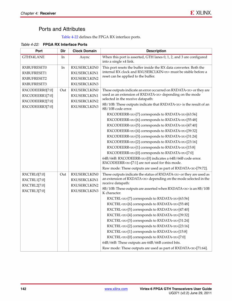
142 www.xilinx.com Virtex-6 FPGA GTH Transceivers User GuideUG371 (v2.2) June 29, 2011
Chapter 4: Receiver
Ports and AttributesTable 4-22 defines the FPGA RX interface ports..
Table 4-22: FPGA RX Interface Ports
Port Dir Clock Domain Description
GTHX4LANE In Async When this port is asserted, GTH lanes 0, 1, 2, and 3 are configured into a single x4 link.
RXBUFRESET0
RXBUFRESET1
RXBUFRESET2
RXBUFRESET3
In RXUSERCLKIN0
RXUSERCLKIN1
RXUSERCLKIN2
RXUSERCLKIN3
This port resets the buffer inside the RX data converter. Both the internal RX clock and RXUSERCLKIN<n> must be stable before a reset can be applied to the buffer.
RXCODEERR0[7:0]
RXCODEERR1[7:0]
RXCODEERR2[7:0]
RXCODEERR3[7:0]
Out RXUSERCLKIN0
RXUSERCLKIN1
RXUSERCLKIN2
RXUSERCLKIN3
These outputs indicate an error occurred on RXDATA<n> or they are used as an extension of RXDATA<n> depending on the mode selected in the receive datapath:
8B/10B: These outputs indicate that RXDATA<n> is the result of an 8B/10B code error.
RXCODEERR<n>[7] corresponds to RXDATA<n>[63:56]
RXCODEERR<n>[6] corresponds to RXDATA<n>[55:48]
RXCODEERR<n>[5] corresponds to RXDATA<n>[47:40]
RXCODEERR<n>[4] corresponds to RXDATA<n>[39:32]
RXCODEERR<n>[3] corresponds to RXDATA<n>[31:24]
RXCODEERR<n>[2] corresponds to RXDATA<n>[23:16]
RXCODEERR<n>[1] corresponds to RXDATA<n>[15:8]
RXCODEERR<n>[0] corresponds to RXDATA<n>[7:0]
64B/66B: RXCODEERR<n>[0] indicates a 64B/66B code error. RXCODEERR<n>[7:1] are not used for this mode.
Raw mode: These outputs are used as part of RXDATA<n>[79:72].
RXCTRL0[7:0]
RXCTRL1[7:0]
RXCTRL2[7:0]
RXCTRL3[7:0]
Out RXUSERCLKIN0
RXUSERCLKIN1
RXUSERCLKIN2
RXUSERCLKIN3
These outputs indicate the status of RXDATA<n> or they are used as an extension of RXDATA<n> depending on the mode selected in the receive datapath:
8B/10B: These outputs are asserted when RXDATA<n> is an 8B/10B K character.
RXCTRL<n>[7] corresponds to RXDATA<n>[63:56]
RXCTRL<n>[6] corresponds to RXDATA<n>[55:48]
RXCTRL<n>[5] corresponds to RXDATA<n>[47:40]
RXCTRL<n>[4] corresponds to RXDATA<n>[39:32]
RXCTRL<n>[3] corresponds to RXDATA<n>[31:24]
RXCTRL<n>[2] corresponds to RXDATA<n>[23:16]
RXCTRL<n>[1] corresponds to RXDATA<n>[15:8]
RXCTRL<n>[0] corresponds to RXDATA<n>[7:0]
64B/66B: These outputs are 64B/66B control bits.
Raw mode: These outputs are used as part of RXDATA<n>[71:64].
Virtex-6 FPGA GTH Transceivers User Guide www.xilinx.com 143UG371 (v2.2) June 29, 2011
FPGA RX Interface
RXDATA0[63:0]
RXDATA1[63:0]
RXDATA2[63:0]
RXDATA3[63:0]
Out RXUSERCLKIN0
RXUSERCLKIN1
RXUSERCLKIN2
RXUSERCLKIN3
This output bus is the receive data bus of the receive interface to the FPGA.
RXUSERCLKIN0
RXUSERCLKIN1
RXUSERCLKIN2
RXUSERCLKIN3
In N/A This port provides a clock for the internal receiver PCS datapath. It is a buffered version of RXUSERCLKOUT<n>.
RXUSERCLKOUT0
RXUSERCLKOUT1
RXUSERCLKOUT2
RXUSERCLKOUT3
Out N/A This output is the recovered clock based on the receiver data bus width and RXRATE<n>. This clock is used to drive RXUSERCLKIN<n> through a buffer.
Table 4-22: FPGA RX Interface Ports (Cont’d)
Port Dir Clock Domain Description

144 www.xilinx.com Virtex-6 FPGA GTH Transceivers User GuideUG371 (v2.2) June 29, 2011
Chapter 4: Receiver
Table 4-23 defines the FPGA RX interface attributes..
Table 4-23: FPGA RX Interface Attributes
Attribute Type Description
BUFFER_CONFIG_LANE0
BUFFER_CONFIG_LANE1
BUFFER_CONFIG_LANE2
BUFFER_CONFIG_LANE3
16-bit Hex Defaults to 16’h4004.
[15:4]: TX_BUFFER_CONFIG[11:0] read pointer adjustment for TX buffer in the data converter.
• For auto adjustment mode, TX_BUFFER_CONFIG[11:0] = 12’h400.• For manual adjustment mode, TX_BUFFER_CONFIG[11:0] settings
depend on TX_FABRIC_WIDTH and if the GTH transceivers within a Quad are configured as a x4 link (GTHX4LANE = 1’b1):• x4 (GTHX4LANE = 1’b1): [TX_FABRIC_WIDTH] = [TX_BUFFER_CONFIG]
“16” or “20” (DRP value 3'b000): 12’h0A4
“32” (DRP value 3'b011): 12’h394
“40” (DRP value 3'b101): 12’h394
“64” (DRP value 3'b010): 12’h250
“80” (DRP value 3'b110): 12’h250
“6466” (DRP value 3'b111): 12’h0A4
• x1 (GTHX4LANE = 1’b0): [TX_FABRIC_WIDTH] = [TX_BUFFER_CONFIG]
“16” or “20” (DRP value 3'b000): 12’h23C
“32” (DRP value 3'b011): 12’h0E8
“40” (DRP value 3'b101): 12’h0E8
“64” (DRP value 3'b010): 12’h3A8
“80” (DRP value 3'b110): 12’h3A8
“6466” (DRP value 3'b111): 12’h23C
[4:0]: RX_BUFFER_CONFIG[3:0] read pointer adjustment for RX buffer in the data converter.
• For auto adjustment mode, RX_BUFFER_CONFIG[3:0] = 0100.• For manual adjustment mode, RX_BUFFER_CONFIG[3:0] settings
depend on RX_FABRIC_WIDTH:
[RX_FABRIC_WIDTH] = [RX_BUFFER_CONFIG]
“16” or “20” (DRP value 3'b000): 4’b0001
“32” (DRP value 3'b011): 4’b0000
“40” (DRP value 3'b101): 4’b0000
“64” (DRP value 3'b010): 4’b0000
“80” (DRP value 3'b110): 4’b0000
“6466” (DRP value 3'b111): 4’b0001

Virtex-6 FPGA GTH Transceivers User Guide www.xilinx.com 145UG371 (v2.2) June 29, 2011
FPGA RX Interface
PCS_MODE_LANE0
PCS_MODE_LANE1
PCS_MODE_LANE2
PCS_MODE_LANE3
16-bit Hex This attribute sets PCS mode.
[15]: Loopback serializer/deserializer RX to serializer/deserializer TX
[14]: Loopback PCS TX to PCS RX
[13:11]: PRBS generator mode
000: None
001: PRBS7
010: PRBS9
011: PRBS11
100: PRBS23
101: PRBS31
Others: Reserved
[10:8]: PRBS checker mode
000: None
001: PRBS7
010: PRBS9
011: PRBS11
100: PRBS23
101: PRBS31
Others: Reserved
[7:4]: PCS RX mode
0000: Zero
0001: 64B/66B
0111: 8B/10B
1010: 16-bit raw data
1011: 20-bit raw data
1100: PRBS
Others: Reserved
[3:0]: PCS TX mode
0000: Zero
0001: 64B/66B
0111: 8B/10B
1010: 16-bit raw data
1011: 20-bit raw data
1100: PRBS
Others: Reserved
Table 4-23: FPGA RX Interface Attributes (Cont’d)
Attribute Type Description

146 www.xilinx.com Virtex-6 FPGA GTH Transceivers User GuideUG371 (v2.2) June 29, 2011
Chapter 4: Receiver
Receive ClockingThe GTH transceiver provides a parallel clock to the FPGA RX interface, RXUSERCLKOUT. The user design must drive this clock to RXUSERCLKIN through either a BUFG or a BUFR. RXUSERCLKIN is the main synchronization clock for all signals into the RX side of the GTH transceiver.
Figure 4-5 is a diagram of the FPGA RX interface clocking.
The user must consider these restrictions for the receive clocking on the GTH transceiver:
• Within a GTH Quad, the four receivers can share one BUFG/BUFR as long as the line rate, fabric data width, decoding, and the clock source on the four links partner transmitting data to the GTH receivers are the same across the four receivers.
If the four link partners do not share the same clock source, then each GTH receiver must have its own BUFG/BUFR.
• The transmitter cannot use the same clock as the receiver; that is, TXUSERCLKIN and RXUSERCLKIN cannot be sourced from the same clock.
RX_FABRIC_WIDTH0
RX_FABRIC_WIDTH1
RX_FABRIC_WIDTH2
RX_FABRIC_WIDTH3
Integer This attribute sets the mapping of the internal data width (PCS) to the external data width (fabric) for the receiver. Valid settings are:
“16” (DRP value 3'b000): PCS to Fabric 1:1
“20” (DRP value 3'b000): PCS to Fabric 1:1
“32” (DRP value 3'b011): PCS to Fabric 1:2 32 bits
“40” (DRP value 3'b101): PCS to Fabric 1:2 40 bits
“64” (DRP value 3'b010): PCS to Fabric 1:4 64 bits
“80” (DRP value 3'b110): PCS to Fabric 1:4 80 bits
“6466” (DRP value 3'b111): 64B/66B mode
Table 4-23: FPGA RX Interface Attributes (Cont’d)
Attribute Type Description
X-Ref Target - Figure 4-5
Figure 4-5: FPGA RX Interface ClockingUG371_c4_01_083109
Internal RXPCS Clock
RX_FABRIC_WIDTH
RXUSERCLKOUT
RXUSERCLKIN
RX Data and Control
RX PCS
RX PCSto Fabric
Designin FPGA
ReceiveClock
Divider
ReceiveData
Converter
GTH Transceiver
BUFGor BUFR
Virtex-6 FPGA GTH Transceivers User Guide www.xilinx.com 147UG371 (v2.2) June 29, 2011
FPGA RX Interface
Configuring the Receiver for Multi-lane ApplicationsTo configure four GTH lanes within a Quad into a single x4 link, the GTHX4LANE port must be tied High. When configured in a single x4 link, a change in the control settings on the master lane also causes the same effect on the slaves, except with the POWERDOWN ports. The POWERDOWN ports of all GTH lanes within a Quad in a x4 link should be driven by the same source.

148 www.xilinx.com Virtex-6 FPGA GTH Transceivers User GuideUG371 (v2.2) June 29, 2011
Chapter 4: Receiver

Virtex-6 FPGA GTH Transceivers User Guide www.xilinx.com 149UG371 (v2.2) June 29, 2011
Chapter 5
Board Design Guidelines
OverviewThis chapter discusses topics related to implementing a design on a printed circuit board (PCB) that uses the Virtex®-6 FPGA GTH transceivers. The GTH transceivers are analog circuits that require special consideration and attention. Besides an understanding of the device pin functionality, an optimal design requires attention to issues such as device interfacing, transmission line impedance and routing, power supply design filtering and distribution, component selection, and PCB layout and stackup design.
Pin Description and Design GuidelinesThis section describes the GTH Quad pins and the termination resistor calibration circuit.
GTH Quad Pin DescriptionsTable 5-1 defines the GTH Quad pins.
Table 5-1: GTH Quad Pin Descriptions
Pins Dir Description
MGTREFCLKPMGTREFCLKN
In (Pad) MGTREFCLKP and MGTREFCLKN are the differential clock input pin pair for the reference clock of the GTHE1_QUAD primitive.
MGTRXP0/MGTRXN0MGTRXP1/MGTRXN1MGTRXP2/MGTRXN2MGTRXP3/MGTRXN3
In (Pad) MGTRXPn and MGTRXNn are the differential input pairs for each of the receivers in the GTHE1_QUAD primitive.
MGTTXP0/MGTTXN0MGTTXP1/MGTTXN1MGTTXP2/MGTTXN2MGTTXP3/MGTTXN3
Out (Pad) MGTTXPn and MGTTXNn are the differential output pairs for each of the transmitters in the GTHE1_QUAD primitive.
MGTRBIAS In (Pad) MGTRBIAS provides internal precision current, voltage, and resistor references for the GTH Quad. This pin should be connected to a 1 k resistor with the other terminal of the resistor connected to ground. Refer to Termination Resistor Calibration Circuit.
MGTHAVCC In (Pad) MGTHAVCC is an analog supply for internal circuits for the receiver and the transmitter.
The nominal voltage is 1.1 VDC

150 www.xilinx.com Virtex-6 FPGA GTH Transceivers User GuideUG371 (v2.2) June 29, 2011
Chapter 5: Board Design Guidelines
Figure 5-1 shows the power supply pin connections for the GTH Quad. The listed voltages are nominal values. Refer to DS152, Virtex-6 FPGA Data Sheet: DC and Switching Characteristics for more detailed information.
Notes relevant to Figure 5-1:
• The voltages shown are nominal values. Refer to DS152, Virtex-6 FPGA Data Sheet: DC and Switching Characteristics for values and tolerances.
• Capacitor symbols are representative.
MGTHAVCCRX In (Pad) MGTHAVCCRX is an analog supply for the PLL and the receiver equalizers.
The nominal voltage is 1.1 VDC
MGTHAVTT In (Pad) MGTHAVTT is an analog supply for the transmit driver.
The nominal voltage is 1.2 VDC
MGTHAVCCPLL In (Pad) MGTHAVCCPLL is an analog supply for the reference clock buffer and the PLL.
The nominal voltage is 1.8 VDC
MGTHAGND N/A MGTHAGND is the ground reference for the GTH transceiver internal circuitry. These pins should be connected to the PCB power supply ground reference plane.
Table 5-1: GTH Quad Pin Descriptions (Cont’d)
Pins Dir Description
X-Ref Target - Figure 5-1
Figure 5-1: Virtex-6 FPGA GTH Transceiver Power Supply Connections
UG371_c5_01_120809
MGTHAVCCPLL
GTH Quad
1.8V
MGTHAVTT
1.2V
MGTHAVCC
1.1V
MGTHAVCCRX
1.1V
MGTRBIAS
1KΩ1%

Virtex-6 FPGA GTH Transceivers User Guide www.xilinx.com 151UG371 (v2.2) June 29, 2011
Board Design Guidelines – Analog Power Supply Pins
Termination Resistor Calibration CircuitEach GTH Quad has one resistor bias circuit (RBIAS). The MGTRBIAS pin connects the RBIAS circuit to an external 1 k 1% resistor. For proper operation of the RBIAS circuit, all GTH transceiver analog power supplies (MGTHAVCC, MGTHAVCCRX, MGTHAVCCPLL, and MGTHAVTT) must be present and within the proper tolerance as specified in DS152, Virtex-6 FPGA Data Sheet: DC and Switching Characteristics.
For reliable operation of the RBIAS circuit, the connection between the RBIAS pin of the FPGA and the pin of the precision resistor must be less than 5 pF and the resistance must be less than 10 .
Board Design Guidelines – Analog Power Supply PinsThe GTH Quad analog power supplies, MGTHAVCC, MGTHAVCCRX, MGTHAVCCPLL, and MGTHAVTT have planes inside the package. For some of the packages, there are two planes for each analog power supply. These planes are designated as left and right planes. The orientation of these planes as left and right is based on the bottom view of the package. Some Virtex-6 HXT FPGAs have GTH Quads only on one side of the package, the right side, while other HXT FPGAs have GTH Quads on both sides of the package.
The GTH Quads on a side are grouped by their common analog power supply connections. There is a left group of GTH Quads and there is a right group of GTH Quads. For each of the analog power supplies, pins for all of the right GTH Quads are connected to common power planes inside the package. Similarly, for each of the analog power supplies, the pins for the left group of GTH Quads are connected to common planes inside the package. As a result, there are four GTH Quad analog power supply planes on each side of the package. On each side of the FPGA that has GTH Quads, there is an MGTHAVCC, MGTHAVCCRX, MGTHAVCCPLL, and MGTHAVTT power plane inside the package.

152 www.xilinx.com Virtex-6 FPGA GTH Transceivers User GuideUG371 (v2.2) June 29, 2011
Chapter 5: Board Design Guidelines
As shown Table 5-2, there are two groupings of the GTH_QUADs columns.
• Devices with two columns of GTH_QUADs
• Left column of GTH_QUADs
• Right column of GTH_QUADs
• Devices with one column of GTH_QUADs on the right-side column
Figure 5-2 shows the orientation in the device of the GTH_QUAD power groups within a device. The type of grouping for the GTH_QUADs in a column depends on the device package. The FF484 and FF784 packages have a single common power plane for each of the MGT supplies. The FF1156 and FF1759 packages have two power planes for each of the MGT power supplies.
Table 5-2: Virtex-6 FPGAs GT Transceivers Grouped by Devices, Packages, and Power Planes
Device/Package
GTX Transceivers GTH Transceivers
Left Side MGT100 MGT101 MGT102 MGT103 MGT104 MGT105 MGT106 MGT107 MGT108
Right Side MGT110 MGT111 MGT112 MGT113 MGT114 MGT115 MGT116 MGT117 MGT118
HX250T-FF1154
Left Side South_L South_L South_L North_L North_L North_L
Right side South_R South_R South_R North_R North_R North_R
HX255T-FF1155
Left Side North_L North_L North_L
Right side North_R North_R North_R Common_R Common_R Common_R
HX255T-FF1923
Left Side North_L North_L North_L Common_L Common_L Common_L
Right side North_R North_R North_R Common_R Common_R Common_R
HX380T-FF1154
Left Side South_L South_L South_L North_L North_L North_L
Right side South_R South_R South_R North_R North_R North_R
HX380T-FF1155
Left Side North_L North_L North_L
Right side North_R North_R North_R Common_R Common_R Common_R
HX380T-FF1923
Left Side South_L South_L South_L North_L North_L North_L Common_L Common_L Common_L
Right side North_R North_R North_R North_R Common_R Common_R Common_R
HX380T-FF1924
Left Side South_L South_L South_L North_L North_L North_L Common_L Common_L Common_L
Right side South_R South_R South_R North_R North_R North_R Common_R Common_R Common_R
HX565T-FF1923
Left Side South_L South_L South_L North_L North_L North_L Common_L Common_L Common_L
Right side North_R North_R North_R North_R Common_R Common_R Common_R
HX565T-FF1924
Left Side South_L South_L South_L North_L North_L North_L Common_L Common_L Common_L
Right side South_L South_L South_L North_R North_R North_R Common_R Common_R Common_R
Notes: 1. Right and left are oriented to the bottom view of the package.2. South_L: South bank GTX power planes on left side of the package.3. North_L: North bank GTX power planes on the left side of the package.4. South_R: South bank GTX power planes on the right side of the package.5. North_R: North bank GTX power planes on the right side of the package.6. Common_L: GTH power planes on the left side of the package.7. Common_R: GTH power planes on the right side of the package.
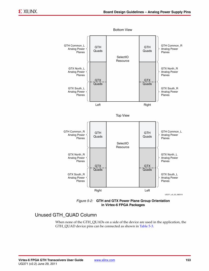
Virtex-6 FPGA GTH Transceivers User Guide www.xilinx.com 153UG371 (v2.2) June 29, 2011
Board Design Guidelines – Analog Power Supply Pins
Unused GTH_QUAD ColumnWhen none of the GTH_QUADs on a side of the device are used in the application, the GTH_QUAD device pins can be connected as shown in Table 5-3.
X-Ref Target - Figure 5-2
Figure 5-2: GTH and GTX Power Plane Group Orientationin Virtex-6 FPGA Packages
Bottom View
Top View
SelectIOResource
SelectIOResource
Left Right
Right Left
GTHQuads
GTHQuads
GTXQuads
GTXQuads
GTHQuads
GTHQuads
GTXQuads
GTXQuads
GTH Common_RAnalog PowerPlanes
GTX North_RAnalog PowerPlanes
GTX South_RAnalog PowerPlanes
GTH Common_LAnalog PowerPlanes
GTX North_LAnalog PowerPlanes
GTX South_LAnalog PowerPlanes
GTH Common_LAnalog Power
Planes
GTX North_LAnalog Power
Planes
GTX South_LAnalog Power
Planes
GTH Common_RAnalog Power
Planes
GTX North_RAnalog Power
Planes
GTX South_RAnalog Power
Planes
UG371_c5_02_082510
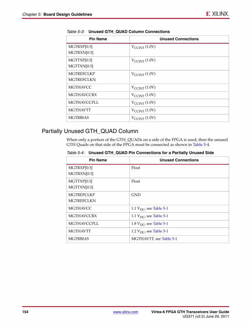
154 www.xilinx.com Virtex-6 FPGA GTH Transceivers User GuideUG371 (v2.2) June 29, 2011
Chapter 5: Board Design Guidelines
Partially Unused GTH_QUAD ColumnWhen only a portion of the GTH_QUADs on a side of the FPGA is used, then the unused GTH Quads on that side of the FPGA must be connected as shown in Table 5-4.
Table 5-3: Unused GTH_QUAD Column Connections
Pin Name Unused Connections
MGTRXP[0:3]
MGTRXN[0:3]
VCCINT (1.0V)
MGTTXP[0:3]
MGTTXN[0:3]
VCCINT (1.0V)
MGTREFCLKP
MGTREFCLKN
VCCINT (1.0V)
MGTHAVCC VCCINT (1.0V)
MGTHAVCCRX VCCINT (1.0V)
MGTHAVCCPLL VCCINT (1.0V)
MGTHAVTT VCCINT (1.0V)
MGTRBIAS VCCINT (1.0V)
Table 5-4: Unused GTH_QUAD Pin Connections for a Partially Unused Side
Pin Name Unused Connections
MGTRXP[0:3]
MGTRXN[0:3]
Float
MGTTXP[0:3]
MGTTXN[0:3]
Float
MGTREFCLKP
MGTREFCLKN
GND
MGTHAVCC 1.1 VDC, see Table 5-1
MGTHAVCCRX 1.1 VDC, see Table 5-1
MGTHAVCCPLL 1.8 VDC, see Table 5-1
MGTHAVTT 1.2 VDC, see Table 5-1
MGTRBIAS MGTHAVTT, see Table 5-1
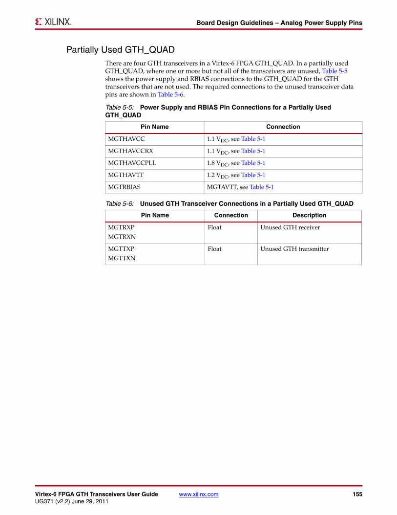
Virtex-6 FPGA GTH Transceivers User Guide www.xilinx.com 155UG371 (v2.2) June 29, 2011
Board Design Guidelines – Analog Power Supply Pins
Partially Used GTH_QUADThere are four GTH transceivers in a Virtex-6 FPGA GTH_QUAD. In a partially used GTH_QUAD, where one or more but not all of the transceivers are unused, Table 5-5 shows the power supply and RBIAS connections to the GTH_QUAD for the GTH transceivers that are not used. The required connections to the unused transceiver data pins are shown in Table 5-6.
Table 5-5: Power Supply and RBIAS Pin Connections for a Partially Used GTH_QUAD
Pin Name Connection
MGTHAVCC 1.1 VDC, see Table 5-1
MGTHAVCCRX 1.1 VDC, see Table 5-1
MGTHAVCCPLL 1.8 VDC, see Table 5-1
MGTHAVTT 1.2 VDC, see Table 5-1
MGTRBIAS MGTAVTT, see Table 5-1
Table 5-6: Unused GTH Transceiver Connections in a Partially Used GTH_QUAD
Pin Name Connection Description
MGTRXP
MGTRXN
Float Unused GTH receiver
MGTTXP
MGTTXN
Float Unused GTH transmitter
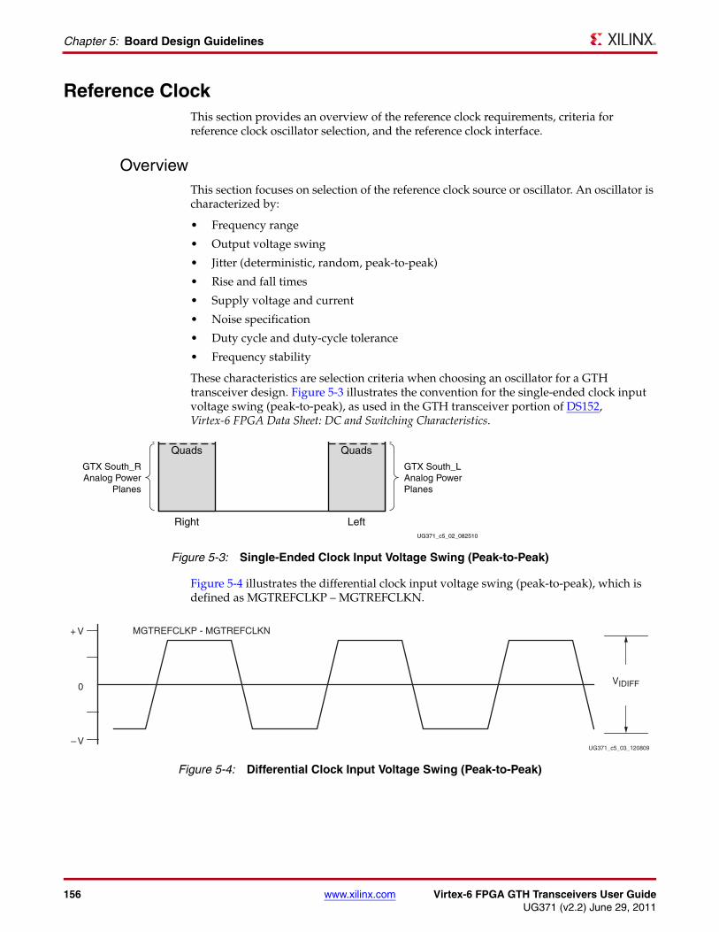
156 www.xilinx.com Virtex-6 FPGA GTH Transceivers User GuideUG371 (v2.2) June 29, 2011
Chapter 5: Board Design Guidelines
Reference ClockThis section provides an overview of the reference clock requirements, criteria for reference clock oscillator selection, and the reference clock interface.
OverviewThis section focuses on selection of the reference clock source or oscillator. An oscillator is characterized by:
• Frequency range
• Output voltage swing
• Jitter (deterministic, random, peak-to-peak)
• Rise and fall times
• Supply voltage and current
• Noise specification
• Duty cycle and duty-cycle tolerance
• Frequency stability
These characteristics are selection criteria when choosing an oscillator for a GTH transceiver design. Figure 5-3 illustrates the convention for the single-ended clock input voltage swing (peak-to-peak), as used in the GTH transceiver portion of DS152, Virtex-6 FPGA Data Sheet: DC and Switching Characteristics.
Figure 5-4 illustrates the differential clock input voltage swing (peak-to-peak), which is defined as MGTREFCLKP – MGTREFCLKN.
X-Ref Target - Figure 5-3
Figure 5-3: Single-Ended Clock Input Voltage Swing (Peak-to-Peak)
Right Left
Quads Quads
GTX South_LAnalog PowerPlanes
GTX South_RAnalog Power
Planes
UG371_c5_02_082510
X-Ref Target - Figure 5-4
Figure 5-4: Differential Clock Input Voltage Swing (Peak-to-Peak)
UG371_c5_03_120809
0
+ V
– V
MGTREFCLKP - MGTREFCLKN
VIDIFF

Virtex-6 FPGA GTH Transceivers User Guide www.xilinx.com 157UG371 (v2.2) June 29, 2011
Reference Clock
Figure 5-5 shows the rise and fall time conventions of the reference clock.
GTH Transceiver Reference Clock ChecklistCertain criteria must be met when choosing an oscillator for a design with GTH transceivers:
• AC coupling must be provided between the oscillator output pins and the dedicated GTH Quad clock input pins.
• The differential voltage swing of the reference clock must have the range specified in DS152, Virtex-6 FPGA Data Sheet: DC and Switching Characteristics. The nominal range is 500 mV–1600 mV and the nominal typical value is 800 mV.
• The reference clock characteristics must meet or exceed those specified in DS152, Virtex-6 FPGA Data Sheet: DC and Switching Characteristics.
• The reference clock characteristics must meet or exceed those specified in the standard for which the GTH transceiver provides physical layer support.
• Requirements set by the oscillator vendor regarding power supply, board layout, and noise specification must be met.
• A dedicated point-to-point connection must be provided between the oscillator and GTH Quad clock input pins.
• Impedance discontinuities on the differential transmission lines must be kept to a minimum because impedance discontinuities generate jitter.
Reference Clock InterfaceThis section discusses the interface between an external reference clock and the GTH transceiver reference clock input. Specifically the interface to an external reference clock with an LVPECL output including AC coupling, pin connections for unused reference clock inputs, and signal integrity issues related to the reference clock circuit.
LVPECL
A reference clock oscillator with an LVPECL output is recommended. An LVDS output reference clock oscillator is not recommended because the LVDS output does not meet the minimum signal amplitude requirements for the GTH transceiver reference clock input. Figure 5-6 provides an example of how to interface an LVPECL output reference clock oscillator to the GTH transceiver reference clock input.
X-Ref Target - Figure 5-5
Figure 5-5: Rise and Fall Times
UG371_c5_04_120809
80%
20%
TFCLK
TRCLK

158 www.xilinx.com Virtex-6 FPGA GTH Transceivers User GuideUG371 (v2.2) June 29, 2011
Chapter 5: Board Design Guidelines
In Figure 5-6, the resistor values shown are nominal values. Refer to the oscillator vendor data sheet for the actual bias resistor requirement.
AC Coupled Reference Clock
AC coupling of the oscillator reference clock output to the GTH Quad reference clock inputs serves multiple purposes:
• It blocks DC current between the oscillator and the GTH Quad dedicated clock input pins. This has the added benefit of reducing the power consumption of both parts.
• Common mode voltage independence is achieved.
• The AC coupling capacitor forms a high-pass filter with the on-chip termination that attenuates reference clock wander.
To minimize noise and power consumption, external AC coupling capacitors between the sourcing oscillator and the GTH Quad dedicated clock reference clock input pins are required.
Unused Reference Clocks
It is recommended to connect the unused differential input pin clock pair (both MGTREFCLKP and MGTREFCLKN) to ground or leave them floating.
Reference Clock Power
The GTH transceiver reference clock input circuit is powered by MGTHAVCCPLL and MGTHAVCCRX. Excessive noise on these supplies has a negative impact on the performance of any GTH Quad that uses the reference clock from this circuit.
X-Ref Target - Figure 5-6
Figure 5-6: Interfacing an LVPECL Oscillator and GTH Transceiver Reference Clock Input
UG371_c5_05_120809
LVPECL Oscillator GTH ReferenceClock Input Buffer
Internal toVirtex-6 FPGA
240Ω
240Ω
0.1 µF
0.1 µF

Virtex-6 FPGA GTH Transceivers User Guide www.xilinx.com 159UG371 (v2.2) June 29, 2011
Power Supplies and Filtering
Power Supplies and FilteringThis section discusses the GTH transceiver power supplies, the two main types of power supply regulators (linear and switching), and performance degradation due to crosstalk.
OverviewThe Virtex-6 FPGA GTH Quad requires four analog power supplies:
• MGTHAVCC, at a nominal voltage level of 1.1 VDC
• MGTHAVCCRX, at a nominal voltage level of 1.1 VDC
• MGTHAVTT, at a nominal voltage level of 1.2 VDC
• MGTHAVCCPLL, at a nominal voltage of 1.8 VDC
Noise on the GTH transceiver analog power supplies can cause degradation in the performance of the transceivers. The most likely form of degradation is an increase in jitter at the output of the GTH transmitter and reduced jitter tolerance in the receiver. Sources of power supply noise are:
• Power supply regulator noise
• The power distribution network
• Coupling from other circuits
Each noise source must be considered in the design and implementation of the GTH transceiver analog power supplies. The total peak-to-peak noise as measured at the input pin of the FPGA should not exceed 10 mVPK-PK.
Power Supply SequencingPlease refer to the DS152, Virtex-6 FPGA Data Sheet: DC and Switching Characteristics Table 27 for power supply sequencing requirements.
Power Supply RegulatorsNormally, the GTH transceiver analog voltage supplies have local power supply regulators that provide a final stage of voltage regulation. Preferably these regulators are placed as close as is feasible to the GTH transceiver power supply pins. Minimizing the distance between the analog voltage regulators and the GTH transceiver power supply pins reduces the opportunity for noise coupling into the supply after the regulator. It also reduces the opportunity for noise generated by current transients caused by load dynamics.
Linear vs. Switching Regulators
The type of power supply regulator used can have a significant impact on the complexity, cost, and performance of the power supply circuit. A power supply regulator must provide adequate power to the GTH transceiver with a minimum amount of noise while meeting the overall system thermal and efficiency requirements. There are two major types of power supply voltage regulators available for regulating the GTH transceiver analog voltage rails: linear regulators and switching regulators. Both have advantages and disadvantages. The optimal choice of regulator type depends on system requirements such as:
• Physical size
160 www.xilinx.com Virtex-6 FPGA GTH Transceivers User GuideUG371 (v2.2) June 29, 2011
Chapter 5: Board Design Guidelines
• Thermal budget
• Power efficiency
• Cost
Linear Regulator
A linear regulator is usually the simplest means to provide voltage regulation for the GTH transceiver analog supply rails. Inherently, a linear regulator does not inject significant noise into the regulated output voltage. In fact some, but not all, linear regulators provide noise rejection at the output from noise present on the voltage input. Another advantage of the linear regulator is that it usually requires a minimal number of external components to realize a circuit on the PCB.
There are potentially two major disadvantages to linear regulators: the minimum dropout voltage and limited efficiency. Linear regulators require an input voltage that is higher than the output voltage. This minimum dropout voltage often is dependent on the load current. Even low dropout linear regulators require a minimum difference between the input voltage and the output voltage of the regulator. The system power supply design must meet the minimum dropout voltage requirements of the linear regulators.
The efficiency of a linear regulator is dependent on the voltage difference between the input and output of the linear regulator. For instance, if the input voltage of the regulator is 2.5 VDC, and the output voltage of the regulator is 1.2 VDC, the voltage difference is 1.3 VDC. Assuming that the current into the regulator is essentially equal to the current out of the regulator, the maximum efficiency of the regulator is 48%. For every watt delivered to the load, the system must consume an additional watt for regulation. This power consumed by the regulator generates heat that must be dissipated by the system. Providing a means to dissipate the heat generated by the linear regulator can drive up the system cost. Therefore, even though linear regulators are less complex and use fewer external components, if the overall system cost is considered (including power consumption and heat dissipation), linear regulators can be at a disadvantage in high current applications.
Switching Regulator
A switching regulator can provide a very efficient means to deliver a well regulated voltage for the GTH transceiver analog power supply. Unlike the linear regulator, the switching regulator does not depend on the voltage drop between the input voltage of the regulator and the output voltage to provide regulation. Therefore, the switching regulator can supply large amounts of current to the load while maintaining high power efficiency. It is not uncommon for a switching regulator to maintain efficiencies of 95% or greater. This efficiency is not severely impacted by the voltage drop between the input of the regulator and the output. Additionally, it is impacted by the load current to a much lesser degree than the linear regulator. Because of the efficiency of the switching regulator, the system does not need to supply as much power to the circuit, and it does not need to provide a means to dissipate power consumed by the regulator.
The disadvantages of the switching regulator are the complexity of the circuit and noise generated by the regulator switching function. Switching regulator circuits are usually more complex than linear regulator circuits. This shortcoming has recently been addressed by several switching regulator component vendors. Normally, a switching power supply regulation circuit requires a switching transistor element, an inductor, and a capacitor. Depending on the required efficiency and load requirements, a switching regulator circuit might require external switching transistors and inductors. In addition, these switching regulators require very careful placement and routing on the PCB to be effective.
Virtex-6 FPGA GTH Transceivers User Guide www.xilinx.com 161UG371 (v2.2) June 29, 2011
Power Supplies and Filtering
Switching regulators generate significant noise and therefore usually require additional filtering before the voltage is delivered to the GTH transceiver analog power supply input of the Virtex-6 FPGA. As mentioned in Overview, page 149, the amplitude of the noise should be limited to less than 10 mVPK-PK. Therefore, the power supply filter should be designed to attenuate the noise from the switching regulator to meet this requirement.

162 www.xilinx.com Virtex-6 FPGA GTH Transceivers User GuideUG371 (v2.2) June 29, 2011
Chapter 5: Board Design Guidelines
Voltage Regulators with Remote Voltage Sensing
The area of the printed circuit board that surrounds the GTH transceiver pins has a number of component placement and routing requirements that make it difficult to place the GTH transceiver analog power-supply voltage regulators in close proximity to the GTH transceiver power-supply pins. As the placement of the power-supply regulators is moved further away from the GTH transceiver power-supply pins, the voltage drop due to current flow in the power distribution network becomes more significant.
By using voltage regulators with a remote voltage sense capability, the voltage regulators can be placed at a greater distance from the FPGA. As illustrated in Figure 5-7, the remote voltage sense circuit allows the voltage regulator circuit to compensate for losses in the power distribution network path between the voltage regulator and the GTH transceiver power supply pins.
Power Supply Distribution Network
Staged Decoupling
Die
There is decoupling capacitance on the die to filter the highest frequency noise components on the power supplies. The internal on-die circuits are the source for this very high-frequency noise.
Package
There is additional decoupling in the Virtex-6 FPGA packages. Decoupling capacitors in the package provide attenuation for noise in the package power plane, thereby reducing the interaction between the GTH Quads. These capacitors in the package also help to maintain a path that is low impedance at high frequencies between the analog power supplies and ground.
Printed Circuit Board
Because the impedance between the power planes and ground has been kept low on the die and in the package, the requirement for decoupling on the PCB is more relaxed. Also,
X-Ref Target - Figure 5-7
Figure 5-7: Power Supply Voltage Regulation with Remote Sense
UG371_c5_07_082510
Power SupplyVoltage Regulator
Power SupplyVoltage Regulator
GTH PowerSupply PIn
VOUTPCB Power Distribution Path
VSENSE
IR Drop between VREGand GTH Power Supply Pin
Voltage is regulated at this location
Note: A voltage regulator with remote voltage sense compensates for IR losses in the path from the voltage regulator to the GTH power supply pin
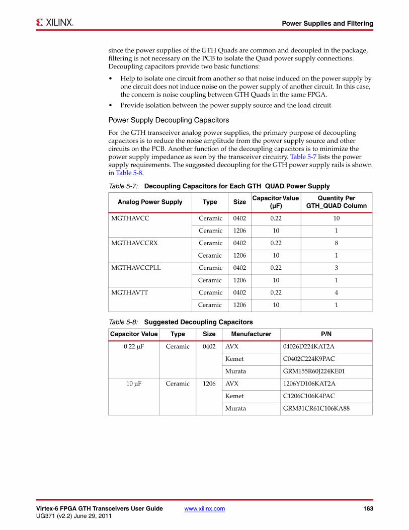
Virtex-6 FPGA GTH Transceivers User Guide www.xilinx.com 163UG371 (v2.2) June 29, 2011
Power Supplies and Filtering
since the power supplies of the GTH Quads are common and decoupled in the package, filtering is not necessary on the PCB to isolate the Quad power supply connections. Decoupling capacitors provide two basic functions:
• Help to isolate one circuit from another so that noise induced on the power supply by one circuit does not induce noise on the power supply of another circuit. In this case, the concern is noise coupling between GTH Quads in the same FPGA.
• Provide isolation between the power supply source and the load circuit.
Power Supply Decoupling Capacitors
For the GTH transceiver analog power supplies, the primary purpose of decoupling capacitors is to reduce the noise amplitude from the power supply source and other circuits on the PCB. Another function of the decoupling capacitors is to minimize the power supply impedance as seen by the transceiver circuitry. Table 5-7 lists the power supply requirements. The suggested decoupling for the GTH power supply rails is shown in Table 5-8.
Table 5-7: Decoupling Capacitors for Each GTH_QUAD Power Supply
Analog Power Supply Type SizeCapacitor Value
(µF)Quantity Per
GTH_QUAD Column
MGTHAVCC Ceramic 0402 0.22 10
Ceramic 1206 10 1
MGTHAVCCRX Ceramic 0402 0.22 8
Ceramic 1206 10 1
MGTHAVCCPLL Ceramic 0402 0.22 3
Ceramic 1206 10 1
MGTHAVTT Ceramic 0402 0.22 4
Ceramic 1206 10 1
Table 5-8: Suggested Decoupling Capacitors
Capacitor Value Type Size Manufacturer P/N
0.22 µF Ceramic 0402 AVX 04026D224KAT2A
Kemet C0402C224K9PAC
Murata GRM155R60J224KE01
10 µF Ceramic 1206 AVX 1206YD106KAT2A
Kemet C1206C106K4PAC
Murata GRM31CR61C106KA88

164 www.xilinx.com Virtex-6 FPGA GTH Transceivers User GuideUG371 (v2.2) June 29, 2011
Chapter 5: Board Design Guidelines
MGTHAVCC Decoupling Capacitor Layout
Minimizing the inductance in the path from the MGTHAVCC power supply pins and the decoupling capacitors is critical. A method for placement and layout for connecting these capacitors to the MGTHAVCC pin vias on the non-component side of the PCB is shown in Figure 5-8. For this example, the layout depends on the use of blind vias for routing the GTH RX/TX data signals. The use of blind vias will result in gaps in the via pin field on the non-component side of the board.
An alternative method for placing the MGTHAVCC de-coupling capacitors is to use filled via-in-pads. An example for placement and layout of the de-coupling capacitors is shown in Figure 5-9.
X-Ref Target - Figure 5-8
Figure 5-8: Placing MGTHAVCC Decoupling Capacitors
1 mm.
1 mm.
BGA Pin Field Vias
Allow For Solder MaskBetween Cap PadsAnd Vias
0402 Capacitor
Blind Via Location(Empty Space on Bottom of Board)
UG371_05_082410

Virtex-6 FPGA GTH Transceivers User Guide www.xilinx.com 165UG371 (v2.2) June 29, 2011
Power Supplies and Filtering
Printed Circuit Board Design
Optimal performance from the GTH transceivers requires careful consideration in the design of the PCB. The areas of PCB design that must be considered are board stackup, component placement, and signal routing. The PCB design includes:
• Power distribution network for MGTHAVCC, MGTHAVCCRX, MGTHAVCCPLL, and MGTHAVTT
• Data lines for the receiver and transmitter
• Reference clock connections between the source oscillator and the GTH reference clock input
• Termination calibration resistor (see Termination Resistor Calibration Circuit)
This subsection discusses the implementation of these designs on the PCB.
GTH Transceiver Power ConnectionsConnections between the GTH power pins and the power distribution network are critical to the overall transceiver performance. The interface between the power distribution network and FPGA must be low impedance and low noise. The maximum noise allowed on the GTH power supplies at the FPGA is 10 mVPP from 10 kHz to 80 MHz.
Signal BGA Breakout
The receiver, transmitter, and reference clock signals must be routed from the BGA pin field to destinations on the PCB. The signal routing layers provide the routing resources for this signal breakout. As shown in Figure 5-10, the signals on the outer rows of BGA pins can be routed using a microstrip on the top layer. These signals are routed to vias where the signal is transitioned from the top microstrip layer to striplines on layer 3. An advantage to
X-Ref Target - Figure 5-9
Figure 5-9: Placing MGTHAVCC Decoupling Capacitors Using Filled Via-in-Pad
1 mm.
1 mm.
BGA Pin Field Vias
Filled Via in Pad
0402 CapacitorUG371_06_082410

166 www.xilinx.com Virtex-6 FPGA GTH Transceivers User GuideUG371 (v2.2) June 29, 2011
Chapter 5: Board Design Guidelines
routing the signals from layer 1 to layer 3 is that the traces on both layers use the plane on layer 2 as the return current reference plane.
For signals that are on the inner rows of pins, it is necessary to route from the BGA pin pad on top of the board to a via. The signal pair is routed from each via by striplines on layers 5 and 7 as shown in Figure 5-11. The Virtex-6 FPGA packages are designed with grounds adjacent to all of the GTH transceiver signal pins. Having adjacent ground pins leads to adjacent BGA breakout vias. The adjacent ground vias provide a return current path for the signal via as the signal propagates from one layer to another layer in the stackup. If the two layers that are connected to the signal via have separate ground planes, the adjacent ground via provides a return current path in the Z-axis and thereby reduces the inductance of the via.X-Ref Target - Figure 5-10
Figure 5-10: TX Microstrip Breakout
Layer 1 Microstrip
Layer 3 Stripline
• Some GTH TX pins are on the outer edge of the FPGA package• Use microstrip to breakout to vias for transition to stripline on layer 3
UG371_c5_11_082510

Virtex-6 FPGA GTH Transceivers User Guide www.xilinx.com 167UG371 (v2.2) June 29, 2011
Power Supplies and Filtering
Crosstalk
A major contributor to degradation in the performance of a GTH transceiver is crosstalk. The mechanisms for crosstalk are aggressor signals coupling into signal traces, coupling into the GTH transceiver power supplies, or a combination of both. The latter is the most common and often the most damaging. Noise coupled into the power supply can corrupt the entire transceiver circuit rather than just a single lane—as in the case of coupling into signal traces. Also, symptoms of noise coupled into the power supply are often more difficult to interpret because the noise is convolved with the normal signals in the transceiver. The result is degradation in the performance of the transceiver that reveals itself as noise in the transmitter output and reduced jitter tolerance in the receiver.
To avoid performance degradation from crosstalk:
• Exposure of power planes to other circuits on the board, such as data lines for memory interfaces and processor buses, should be monitored.
• Adequate filtering should be provided to the GTH transceiver power supplies near the point of the load. The amount of filtering should be determined by the magnitude and frequency of the signal from potential noise sources. Noise on the GTH transceiver power supplies should be kept below 10 mVPK-PK from 10 KHz to 80 MHz.
• Return current paths of signal traces in the vicinity of the GTH transceiver power distribution network should be monitored. Besides broadband and edge coupling of traces on the same or adjacent layers, coupling from aggressor traces can occur if the aggressor signal is propagating from one layer to another, each layer having a different reference plane. As the signal propagates through the portion of the via that does not have a return current path, it generates return currents in the next lowest impedance structure on the board. A victim of this unintended return current path could be a signal or power via for the GTH transceivers.
X-Ref Target - Figure 5-11
Figure 5-11: RX BGA Breakout to Stripline
View Of Layers 1 Through 7 View Of Layer 7
Layer 7 Stripline
• For GTH TX/RX pins that are not on the outer edge of the FPGA package• Use stripline from dog-bone via to breakout from BGA pin pad• Since outer pin signals do not have vias, the resulting via gap provides routing paths for inner BGA pin breakout
UG371_c5_12_082510
168 www.xilinx.com Virtex-6 FPGA GTH Transceivers User GuideUG371 (v2.2) June 29, 2011
Chapter 5: Board Design Guidelines
SelectIO Interface Usage GuidelinesBecause the GTH transceiver’s performance can degrade in an environment flooded with SelectIO™ interface activity, it is important to have guidelines for SelectIO interface usage that minimize the impact on GTH transceiver performance.
The pinout for the Virtex-6 FPGA package maintains a physical separation between the GTH transceiver pins and the SelectIO interface pins. Because of this separation in the package pinout, no SelectIO interface pins need to be excluded when using the GTH transceivers.
Even though the Virtex-6 FPGA package pinout eliminates the crosstalk between the SelectIO interface and the GTH transceiver pins due to pin adjacency, it is still possible to induce crosstalk on the PCB. Therefore, when routing signals on the PCB:
• Routing of GTH transceiver signals and SelectIO interface signals on adjacent layers should be eliminated. If these signals are routed on adjacent layers there is potential for broadside coupling.
• Isolation of the return current paths should be maintained for both the SelectIO interface signals and the GTH transceiver signals, including both traces and vias.
• SelectIO interface signals should not be routed over or through the GTH transceiver power islands. The power islands for the GTH transceivers are also a potential source for SelectIO interface induced noise.

Virtex-6 FPGA GTH Transceivers User Guide www.xilinx.com 169UG371 (v2.2) June 29, 2011
Appendix A
Low Latency Design of GTH Transceivers
Low Latency Design of GTH TransceiversThis appendix illustrates the latency of the different functional blocks inside the TX and the RX sections of the GTH transceiver.
Table A-1 shows the latencies of the TX and RX sections for the various modes of the GTH transceiver.
Table A-1: Latency of RX and TX Sections in the GTH Transceiver
Fabric Interface
Fabric Interface FIFO
TX
Fabric Interface FIFO
RX PCS (TX) PCS (RX) PMA (TX) PMA (RX)
min max min max min max min max min max min max
UI UI UI UI UI UI UI UI UI UI UI UI
RAW16 16 64 16 64 48 64 48 64 2 2 17 17
RAW32 32 128 32 128 48 64 48 64 2 2 17 17
RAW64 64 256 64 256 48 64 48 64 2 2 17 17
RAW20 20 80 20 80 60 80 60 80 2 2 21 21
RAW40 40 160 40 160 60 80 60 80 2 2 21 21
RAW80 80 320 80 320 60 80 60 80 2 2 21 21
8B10B 16 16 64 16 64 80 100 80 100 2 2 21 21
8B10B 32 32 128 32 128 80 100 80 100 2 2 21 21
8B10B 64 64 256 64 256 80 100 80 100 2 2 21 21
64B/66B 64 256 64 256 178 226 278 376 2 2 17 17
170 www.xilinx.com Virtex-6 FPGA GTH Transceivers User GuideUG371 (v2.2) June 29, 2011
Appendix A: Low Latency Design of GTH Transceivers

Virtex-6 FPGA GTH Transceivers User Guide www.xilinx.com 171UG371 (v2.2) June 29, 2011
Appendix B
DRP Address Map of GTH Transceivers
DRP Address Map of the GTH TransceiversTable B-1 and Table B-2 list the DRP map sorted by attribute names.
Table B-1: GTH_QUAD Attributes
Attribute Name TypeConfiguration
Memory (DRP Address)
GTH Registers(DRP Address)
GTH Registers(MGMT with
MMD Address)
BER_CONST_PTRN0 16-bit Hex 0x0053 0x7000 0xC000 – 0x03
BER_CONST_PTRN1 16-bit Hex 0x0054 0x7001 0xC001 – 0x03
BUFFER_CONFIG_LANE0 16-bit Hex 0x004F N/A N/A
BUFFER_CONFIG_LANE1 0x0052
BUFFER_CONFIG_LANE2 0x00F0
BUFFER_CONFIG_LANE3 0x00ED
DFE_TRAIN_CTRL_LANE0 16-bit Hex 0x003A 0x4015 0x8015 – 0x01
DFE_TRAIN_CTRL_LANE1 0x008A 0x4115
DFE_TRAIN_CTRL_LANE2 0x00C2 0x4215
DFE_TRAIN_CTRL_LANE3 0x0105 0x4315
DLL_CFG0 16-bit Hex 0x0011 0x6002 0xC002 – 0x01
DLL_CFG1 16-bit Hex 0x0022 0x601D 0xC01D – 0x01
E10GBASEKR_LD_COEFF_UPD_LANE0 16-bit Hex 0x000D 0x209A 0x009A – 0x01
E10GBASEKR_LD_COEFF_UPD_LANE1 0x0073 0x219A
E10GBASEKR_LD_COEFF_UPD_LANE2 0x00AB 0x229A
E10GBASEKR_LD_COEFF_UPD_LANE3 0x00E7 0x239A
E10GBASEKR_LP_COEFF_UPD_LANE0 16-bit Hex 0x000C 0x2098 0x0098 – 0x01
E10GBASEKR_LP_COEFF_UPD_LANE1 0x0072 0x2198
E10GBASEKR_LP_COEFF_UPD_LANE2 0x00AA 0x2298
E10GBASEKR_LP_COEFF_UPD_LANE3 0x00E6 0x2398
172 www.xilinx.com Virtex-6 FPGA GTH Transceivers User GuideUG371 (v2.2) June 29, 2011
Appendix B: DRP Address Map of GTH Transceivers
E10GBASEKR_PMA_CTRL_LANE0 16-bit Hex 0x000B 0x2096 0x0096 – 0x01
E10GBASEKR_PMA_CTRL_LANE1 0x0071 0x2196
E10GBASEKR_PMA_CTRL_LANE2 0x00A9 0x2296
E10GBASEKR_PMA_CTRL_LANE3 0x00E5 0x2396
E10GBASEKX_CTRL_LANE0 16-bit Hex 0x000E 0x20A0 0x00A0 – 0x01
E10GBASEKX_CTRL_LANE1 0x0074 0x21A0
E10GBASEKX_CTRL_LANE2 0x00AC 0x22A0
E10GBASEKX_CTRL_LANE3 0x00E8 0x23A0
E10GBASER_PCS_CFG_LANE0 16-bit Hex 0x0062 0x5080 0x8080 – 0x03
E10GBASER_PCS_CFG_LANE1 0x00A5 0x5180
E10GBASER_PCS_CFG_LANE2 0x00DD 0x5280
E10GBASER_PCS_CFG_LANE3 0x120 0x5380
E10GBASER_PCS_SEEDA0_LANE0 16-bit Hex 0x0043 0x3022 0x0022 – 0x03
E10GBASER_PCS_SEEDA0_LANE1 0x0093 0x3122
E10GBASER_PCS_SEEDA0_LANE2 0x00CB 0x3222
E10GBASER_PCS_SEEDA0_LANE3 0x010E 0x3322
E10GBASER_PCS_SEEDA1_LANE0 16-bit Hex 0x0044 0x3023 0x0023 – 0x03
E10GBASER_PCS_SEEDA1_LANE1 0x0094 0x3123
E10GBASER_PCS_SEEDA1_LANE2 0x00CC 0x3223
E10GBASER_PCS_SEEDA1_LANE3 0x010F 0x3323
E10GBASER_PCS_SEEDA2_LANE0 16-bit Hex 0x0045 0x3024 0x0024 – 0x03
E10GBASER_PCS_SEEDA2_LANE1 0x0095 0x3124
E10GBASER_PCS_SEEDA2_LANE2 0x00CD 0x3224
E10GBASER_PCS_SEEDA2_LANE3 0x0110 0x3324
E10GBASER_PCS_SEEDA3_LANE0 16-bit Hex 0x0046 0x3025 0x0025 – 0x03
E10GBASER_PCS_SEEDA3_LANE1 0x0096 0x3125
E10GBASER_PCS_SEEDA3_LANE2 0x00CE 0x3225
E10GBASER_PCS_SEEDA3_LANE3 0x0111 0x3325
E10GBASER_PCS_SEEDB0_LANE0 16-bit Hex 0x0047 0x3026 0x0026 – 0x03
E10GBASER_PCS_SEEDB0_LANE1 0x0097 0x3126
E10GBASER_PCS_SEEDB0_LANE2 0x00CF 0x3226
E10GBASER_PCS_SEEDB0_LANE3 0x0112 0x3326
Table B-1: GTH_QUAD Attributes (Cont’d)
Attribute Name TypeConfiguration
Memory (DRP Address)
GTH Registers(DRP Address)
GTH Registers(MGMT with
MMD Address)

Virtex-6 FPGA GTH Transceivers User Guide www.xilinx.com 173UG371 (v2.2) June 29, 2011
DRP Address Map of the GTH Transceivers
E10GBASER_PCS_SEEDB1_LANE0 16-bit Hex 0x0048 0x3027 0x0027 – 0x03
E10GBASER_PCS_SEEDB1_LANE1 0x0098 0x3127
E10GBASER_PCS_SEEDB1_LANE2 0x00D0 0x3227
E10GBASER_PCS_SEEDB1_LANE3 0x0113 0x3327
E10GBASER_PCS_SEEDB2_LANE0 16-bit Hex 0x0049 0x3028 0x0028 – 0x03
E10GBASER_PCS_SEEDB2_LANE1 0x0099 0x3128
E10GBASER_PCS_SEEDB2_LANE2 0x00D1 0x3228
E10GBASER_PCS_SEEDB2_LANE3 0x0114 0x3328
E10GBASER_PCS_SEEDB3_LANE0 16-bit Hex 0x004A 0x3029 0x0029 – 0x03
E10GBASER_PCS_SEEDB3_LANE1 0x009A 0x3129
E10GBASER_PCS_SEEDB3_LANE2 0x00D2 0x3229
E10GBASER_PCS_SEEDB3_LANE3 0x0115 0x3329
E10GBASER_PCS_TEST_CTRL_LANE0 16-bit Hex 0x004B 0x302A 0x002A – 0x03
E10GBASER_PCS_TEST_CTRL_LANE1 0x009B 0x312A
E10GBASER_PCS_TEST_CTRL_LANE2 0x00D3 0x322A
E10GBASER_PCS_TEST_CTRL_LANE3 0x0116 0x332A
E10GBASEX_PCS_TSTCTRL_LANE0 16-bit Hex 0x0042 0x3019 0x0019 – 0x03
E10GBASEX_PCS_TSTCTRL_LANE1 0x0092 0x3119
E10GBASEX_PCS_TSTCTRL_LANE2 0x00CA 0x3219
E10GBASEX_PCS_TSTCTRL_LANE3 0x010D 0x3319
GLBL0_NOISE_CTRL 16-bit Hex 0x0018 0x600C 0xC00C- 0x01
GLBL_AMON_SEL 16-bit Hex 0x0014 0x6006 0xC006 – 0x01
GLBL_DMON_SEL 16-bit Hex 0x0016 0x6008 0xC008 – 0x01
GTH_CFG_PWRUP_LANE0 1-bit Binary 0x004E[1] N/A N/A
GTH_CFG_PWRUP_LANE1 0x0051[1] N/A N/A
GTH_CFG_PWRUP_LANE2 0x00F1[1] N/A N/A
GTH_CFG_PWRUP_LANE3 0x00EE[1] N/A N/A
GLBL_PWR_CTRL 16-bit Hex 0x0020 0x601A 0xC01A – 0x01
LANE_AMON_SEL 16-bit Hex 0x0015 0x6007 0xC007 – 0x01
LANE_DMON_SEL 16-bit Hex 0x0017 0x6009 0xC009 – 0x01
LANE_LNK_CFGOVRD 16-bit Hex 0x0055 0x7003 0xC003 – 0x03
Table B-1: GTH_QUAD Attributes (Cont’d)
Attribute Name TypeConfiguration
Memory (DRP Address)
GTH Registers(DRP Address)
GTH Registers(MGMT with
MMD Address)

174 www.xilinx.com Virtex-6 FPGA GTH Transceivers User GuideUG371 (v2.2) June 29, 2011
Appendix B: DRP Address Map of GTH Transceivers
LANE_PWR_CTRL_LANE0 16-bit Hex 0x003B 0x4016 0x8016 – 0x01
LANE_PWR_CTRL_LANE1 0x008B 0x4116
LANE_PWR_CTRL_LANE2 0x00C3 0x4216
LANE_PWR_CTRL_LANE3 0x0106 0x4316
LNK_TRN_CFG_LANE0 16-bit Hex 0x003E 0x4030 0x8030 – 0x01
LNK_TRN_CFG_LANE1 0x008E 0x4130
LNK_TRN_CFG_LANE2 0x00C6 0x4230
LNK_TRN_CFG_LANE3 0x0109 0x4330
LNK_TRN_COEFF_REQ_LANE0 16-bit Hex 0x003F 0x4031 0x8031 – 0x01
LNK_TRN_COEFF_REQ_LANE1 0x008F 0x4131
LNK_TRN_COEFF_REQ_LANE2 0x00C7 0x4231
LNK_TRN_COEFF_REQ_LANE3 0x010A 0x4331
MISC_CFG 16-bit Hex 0x0012 0x6003 0xC003 – 0x01
MODE_CFG1 16-bit Hex 0x0067 N/A N/A
MODE_CFG2 16-bit Hex 0x0068 N/A N/A
MODE_CFG3 16-bit Hex 0x0069 N/A N/A
MODE_CFG4 16-bit Hex 0x006A N/A N/A
MODE_CFG5 16-bit Hex 0x006B N/A N/A
MODE_CFG6 16-bit Hex 0x006C N/A N/A
MODE_CFG7 16-bit Hex 0x006D N/A N/A
PCS_ABILITY_LANE0 16-bit Hex 0x0060 0x5040 0x8040 – 0x03
PCS_ABILITY_LANE1 0x00A3 0x5140
PCS_ABILITY_LANE2 0x00DB 0x5240
PCS_ABILITY_LANE3 0x011E 0x5340
PCS_CTRL1_LANE0 16-bit Hex 0x0040 0x3000 0x0000 – 0x03
PCS_CTRL1_LANE1 0x0090 0x3100
PCS_CTRL1_LANE2 0x00C8 0x3200
PCS_CTRL1_LANE3 0x010B 0x3300
PCS_CTRL2_LANE0 16-bit Hex 0x0041 0x3007 0x0007 – 0x03
PCS_CTRL2_LANE1 0x0091 0x3107
PCS_CTRL2_LANE2 0x00C9 0x3207
PCS_CTRL2_LANE3 0x010C 0x3307
Table B-1: GTH_QUAD Attributes (Cont’d)
Attribute Name TypeConfiguration
Memory (DRP Address)
GTH Registers(DRP Address)
GTH Registers(MGMT with
MMD Address)

Virtex-6 FPGA GTH Transceivers User Guide www.xilinx.com 175UG371 (v2.2) June 29, 2011
DRP Address Map of the GTH Transceivers
PCS_MISC_CFG_0_LANE0 16-bit Hex 0x0059 0x5001 0x8001 – 0x03
PCS_MISC_CFG_0_LANE1 0x009C 0x5101
PCS_MISC_CFG_0_LANE2 0x00D4 0x5201
PCS_MISC_CFG_0_LANE3 0x0117 0x5301
PCS_MISC_CFG_1_LANE0 16-bit Hex 0x005E 0x500D 0x800D – 0x03
PCS_MISC_CFG_1_LANE1 0x00A1 0x510D
PCS_MISC_CFG_1_LANE2 0x00D9 0x520D
PCS_MISC_CFG_1_LANE3 0x011C 0x530D
PCS_MODE_LANE0 16-bit Hex 0x004C 0x5000 0x8000 – 0x03
PCS_MODE_LANE1 0x0050 0x5100
PCS_MODE_LANE2 0x00F3 0x5200
PCS_MODE_LANE3 0x00EF 0x5300
PCS_RESET_LANE0 16-bit Hex 0x005C 0x5009 0x8009 – 0x03
PCS_RESET_LANE1 0x009F 0x5109
PCS_RESET_LANE2 0x00D7 0x5209
PCS_RESET_LANE3 0x011A 0x5309
PCS_RESET_1_LANE0 16-bit Hex 0x005F 0x500F 0x800F – 0x03
PCS_RESET_1_LANE1 0x00A2 0x510F
PCS_RESET_1_LANE2 0x00DA 0x520F
PCS_RESET_1_LANE3 0x011D 0x530F
PCS_TYPE_LANE0 16-bit Hex 0x0061 0x5041 0x8041 – 0x03
PCS_TYPE_LANE1 0x00A4 0x5141
PCS_TYPE_LANE2 0x00DC 0x5241
PCS_TYPE_LANE3 0x011F 0x5341
PLL_CFG0 16-bit Hex 0x000F 0x6000 0xC000 – 0x01
PLL_CFG1 16-bit Hex 0x0010 0x6001 0xC001 – 0x01
PLL_CFG2 16-bit Hex 0x0019 0x6011 0xC011 – 0x01
PMA_CTRL1_LANE0 16-bit Hex 0x0008 0x2000 0x0000 – 0x01
PMA_CTRL1_LANE1 0x006E 0x2100
PMA_CTRL1_LANE2 0x00A6 0x2200
PMA_CTRL1_LANE3 0x00E2 0x2300
Table B-1: GTH_QUAD Attributes (Cont’d)
Attribute Name TypeConfiguration
Memory (DRP Address)
GTH Registers(DRP Address)
GTH Registers(MGMT with
MMD Address)

176 www.xilinx.com Virtex-6 FPGA GTH Transceivers User GuideUG371 (v2.2) June 29, 2011
Appendix B: DRP Address Map of GTH Transceivers
PMA_CTRL2_LANE0 16-bit Hex 0x0009 0x2007 0x0007 – 0x01
PMA_CTRL2_LANE1 0x006F 0x2107
PMA_CTRL2_LANE2 0x00A7 0x2207
PMA_CTRL2_LANE3 0x00E3 0x2307
PMA_LPBK_CTRL_LANE0 16-bit Hex 0x0039 0x4014 0x8014 – 0x01
PMA_LPBK_CTRL_LANE1 0x0089 0x4114
PMA_LPBK_CTRL_LANE2 0x00C1 0x4214
PMA_LPBK_CTRL_LANE3 0x0104 0x4314
PRBS_BER_CFG0_LANE0 16-bit Hex 0x005A 0x5007 0x8007 – 0x03
PRBS_BER_CFG0_LANE1 0x009D 0x5107
PRBS_BER_CFG0_LANE2 0x00D5 0x5207
PRBS_BER_CFG0_LANE3 0x0118 0x5307
PRBS_BER_CFG1_LANE0 16-bit Hex 0x005B 0x5008 0x8008 – 0x03
PRBS_BER_CFG1_LANE1 0x009E 0x5108
PRBS_BER_CFG1_LANE2 0x00D6 0x5208
PRBS_BER_CFG1_LANE3 0x0119 0x5308
PRBS_CFG_LANE0 16-bit Hex 0x005D 0x500C 0x800C – 0x03
PRBS_CFG_LANE1 0x00A0 0x510C
PRBS_CFG_LANE2 0x00D8 0x520C
PRBS_CFG_LANE3 0x011B 0x530C
PTRN_CFG0_LSB 16-bit Hex 0x0056 0x7005 0xC005 – 0x03
PTRN_CFG0_MSB 16-bit Hex 0x0057 0x7006 0xC006 – 0x03
PTRN_LEN_CFG 16-bit Hex 0x0058 0x7007 0xC007 – 0x03
PWRUP_DLY 16-bit Hex 0x0021 0x601C 0xC01C – 0x01
RX_AEQ_MON0_LANE0 16-bit hex N/A 0x4020 0x8020 - 0x01
RX_AEQ_MON0_LANE1 0x4120
RX_AEQ_MON0_LANE2 0x4220
RX_AEQ_MON0_LANE3 0x4320
RX_AEQ_MON1_LANE0 16-bit hex N/A 0x4021 0x8021 - 0x01
RX_AEQ_MON1_LANE1 0x4121
RX_AEQ_MON1_LANE2 0x4221
RX_AEQ_MON1_LANE3 0x4321
Table B-1: GTH_QUAD Attributes (Cont’d)
Attribute Name TypeConfiguration
Memory (DRP Address)
GTH Registers(DRP Address)
GTH Registers(MGMT with
MMD Address)

Virtex-6 FPGA GTH Transceivers User Guide www.xilinx.com 177UG371 (v2.2) June 29, 2011
DRP Address Map of the GTH Transceivers
RX_AEQ_VAL0_LANE0 16-bit Hex 0x002F 0x400A 0x800A – 0x01
RX_AEQ_VAL0_LANE1 0x007F 0x410A
RX_AEQ_VAL0_LANE2 0x00B7 0x420A
RX_AEQ_VAL0_LANE3 0x00FA 0x430A
RX_AEQ_VAL1_LANE0 16-bit Hex 0x0030 0x400B 0x800B – 0x01
RX_AEQ_VAL1_LANE1 0x0080 0x410B
RX_AEQ_VAL1_LANE2 0x00B8 0x420B
RX_AEQ_VAL1_LANE3 0x00FB 0x430B
RX_AGC_CTRL_LANE0 16-bit Hex 0x0028 0x4003 0x8003 – 0x01
RX_AGC_CTRL_LANE1 0x0078 0x4103
RX_AGC_CTRL_LANE2 0x00B0 0x4203
RX_AGC_CTRL_LANE3 0x00EC 0x4303
RX_CDR_CTRL0_LANE0 16-bit Hex 0x002A 0x4005 0x8005 – 0x01
RX_CDR_CTRL0_LANE1 0x007A 0x4105
RX_CDR_CTRL0_LANE2 0x00B2 0x4205
RX_CDR_CTRL0_LANE3 0x00F5 0x4305
RX_CDR_CTRL1_LANE0 16-bit Hex 0x002B 0x4006 0x8006 – 0x01
RX_CDR_CTRL1_LANE1 0x007B 0x4106
RX_CDR_CTRL1_LANE2 0x00B3 0x4206
RX_CDR_CTRL1_LANE3 0x00F6 0x4306
RX_CDR_CTRL2_LANE0 16-bit Hex 0x002C 0x4007 0x8007 – 0x01
RX_CDR_CTRL2_LANE1 0x007C 0x4107
RX_CDR_CTRL2_LANE2 0x00B4 0x4207
RX_CDR_CTRL2_LANE3 0x00F7 0x4307
RX_CFG0_LANE0 16-bit Hex 0x0025 0x4000 0x8000 – 0x01
RX_CFG0_LANE1 0x0075 0x4100
RX_CFG0_LANE2 0x00AD 0x4200
RX_CFG0_LANE3 0x00E9 0x4300
RX_CFG1_LANE0 16-bit Hex 0x0026 0x4001 0x8001 – 0x01
RX_CFG1_LANE1 0x0076 0x4101
RX_CFG1_LANE2 0x00AE 0x4201
RX_CFG1_LANE3 0x00EA 0x4301
Table B-1: GTH_QUAD Attributes (Cont’d)
Attribute Name TypeConfiguration
Memory (DRP Address)
GTH Registers(DRP Address)
GTH Registers(MGMT with
MMD Address)

178 www.xilinx.com Virtex-6 FPGA GTH Transceivers User GuideUG371 (v2.2) June 29, 2011
Appendix B: DRP Address Map of GTH Transceivers
RX_CFG2_LANE0 16-bit Hex 0x0027 0x4002 0x8002 – 0x01
RX_CFG2_LANE1 0x0077 0x4102
RX_CFG2_LANE2 0x00AF 0x4202
RX_CFG2_LANE3 0x00EB 0x4302
RX_CTLE_CTRL_LANE0 16-bit Hex 0x0031 0x400C 0x800C – 0x01
RX_CTLE_CTRL_LANE1 0x0081 0x410C
RX_CTLE_CTRL_LANE2 0x00B9 0x420C
RX_CTLE_CTRL_LANE3 0x00FC 0x430C
RX_CTRL_OVRD_LANE0 16-bit Hex 0x003D 0x401E 0x801E – 0x01
RX_CTRL_OVRD_LANE1 0x008D 0x411E
RX_CTRL_OVRD_LANE2 0x00C5 0x420E
RX_CTRL_OVRD_LANE3 0x0108 0x430E
RX_FABRIC_WIDTH0 Integer 0x004E[11:9] N/A N/A
RX_FABRIC_WIDTH1 0x0051[11:9]
RX_FABRIC_WIDTH2 0x00F1[11:9]
RX_FABRIC_WIDTH3 0x00EE[11:9]
RX_LOOP_CTRL_LANE0 16-bit Hex 0x0029 0x4004 0x8004 – 0x01
RX_LOOP_CTRL_LANE1 0x0079 0x4104
RX_LOOP_CTRL_LANE2 0x00B1 0x4204
RX_LOOP_CTRL_LANE3 0x00F4 0x4304
RX_MVAL0_LANE0 16-bit Hex 0x002D 0x4008 0x8008 – 0x01
RX_MVAL0_LANE1 0x007D 0x4108
RX_MVAL0_LANE2 0x00B5 0x4208
RX_MVAL0_LANE3 0x00F8 0x4308
RX_MVAL1_LANE0 16-bit Hex 0x002E 0x4009 0x8009 – 0x01
RX_MVAL1_LANE1 0x007E 0x4109
RX_MVAL1_LANE2 0x00B6 0x4209
RX_MVAL1_LANE3 0x00F9 0x4309
RX_P0_CTRL 16-bit Hex 0x001A 0x6014 0xC014 – 0x01
RX_P0S_CTRL 16-bit Hex 0x001B 0x6015 0xC015 – 0x01
RX_P1_CTRL 16-bit Hex 0x001C 0x6016 0xC016 – 0x01
RX_P2_CTRL 16-bit Hex 0x001D 0x6017 0xC017 – 0x01
Table B-1: GTH_QUAD Attributes (Cont’d)
Attribute Name TypeConfiguration
Memory (DRP Address)
GTH Registers(DRP Address)
GTH Registers(MGMT with
MMD Address)
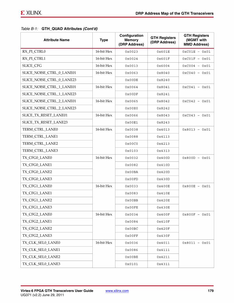
Virtex-6 FPGA GTH Transceivers User Guide www.xilinx.com 179UG371 (v2.2) June 29, 2011
DRP Address Map of the GTH Transceivers
RX_PI_CTRL0 16-bit Hex 0x0023 0x601E 0xC01E – 0x01
RX_PI_CTRL1 16-bit Hex 0x0024 0x601F 0xC01F – 0x01
SLICE_CFG 16-bit Hex 0x0013 0x6004 0xC004 – 0x01
SLICE_NOISE_CTRL_0_LANE01 16-bit Hex 0x0063 0x8040 0xC040 – 0x01
SLICE_NOISE_CTRL_0_LANE23 0x00DE 0x8240
SLICE_NOISE_CTRL_1_LANE01 16-bit Hex 0x0064 0x8041 0xC041 – 0x01
SLICE_NOISE_CTRL_1_LANE23 0x00DF 0x8241
SLICE_NOISE_CTRL_2_LANE01 16-bit Hex 0x0065 0x8042 0xC042 – 0x01
SLICE_NOISE_CTRL_2_LANE23 0x00E0 0x8242
SLICE_TX_RESET_LANE01 16-bit Hex 0x0066 0x8043 0xC043 – 0x01
SLICE_TX_RESET_LANE23 0x00E1 0x8243
TERM_CTRL_LANE0 16-bit Hex 0x0038 0x4013 0x8013 – 0x01
TERM_CTRL_LANE1 0x0088 0x4113
TERM_CTRL_LANE2 0x00C0 0x4213
TERM_CTRL_LANE3 0x0103 0x4313
TX_CFG0_LANE0 16-bit Hex 0x0032 0x400D 0x800D – 0x01
TX_CFG0_LANE1 0x0082 0x410D
TX_CFG0_LANE2 0x00BA 0x420D
TX_CFG0_LANE3 0x00FD 0x430D
TX_CFG1_LANE0 16-bit Hex 0x0033 0x400E 0x800E – 0x01
TX_CFG1_LANE1 0x0083 0x410E
TX_CFG1_LANE2 0x00BB 0x420E
TX_CFG1_LANE3 0x00FE 0x430E
TX_CFG2_LANE0 16-bit Hex 0x0034 0x400F 0x800F – 0x01
TX_CFG2_LANE1 0x0084 0x410F
TX_CFG2_LANE2 0x00BC 0x420F
TX_CFG2_LANE3 0x00FF 0x430F
TX_CLK_SEL0_LANE0 16-bit Hex 0x0036 0x4011 0x8011 – 0x01
TX_CLK_SEL0_LANE1 0x0086 0x4111
TX_CLK_SEL0_LANE2 0x00BE 0x4211
TX_CLK_SEL0_LANE3 0x0101 0x4311
Table B-1: GTH_QUAD Attributes (Cont’d)
Attribute Name TypeConfiguration
Memory (DRP Address)
GTH Registers(DRP Address)
GTH Registers(MGMT with
MMD Address)
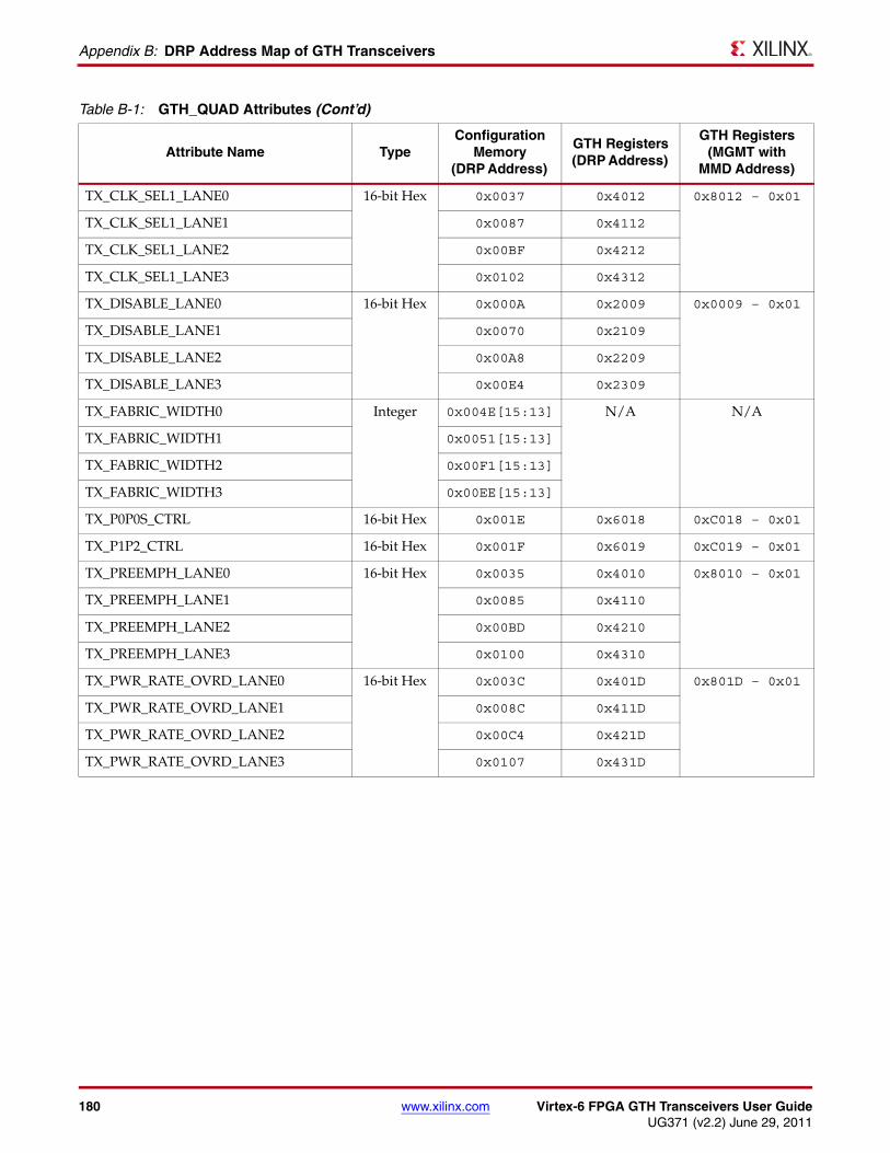
180 www.xilinx.com Virtex-6 FPGA GTH Transceivers User GuideUG371 (v2.2) June 29, 2011
Appendix B: DRP Address Map of GTH Transceivers
TX_CLK_SEL1_LANE0 16-bit Hex 0x0037 0x4012 0x8012 – 0x01
TX_CLK_SEL1_LANE1 0x0087 0x4112
TX_CLK_SEL1_LANE2 0x00BF 0x4212
TX_CLK_SEL1_LANE3 0x0102 0x4312
TX_DISABLE_LANE0 16-bit Hex 0x000A 0x2009 0x0009 – 0x01
TX_DISABLE_LANE1 0x0070 0x2109
TX_DISABLE_LANE2 0x00A8 0x2209
TX_DISABLE_LANE3 0x00E4 0x2309
TX_FABRIC_WIDTH0 Integer 0x004E[15:13] N/A N/A
TX_FABRIC_WIDTH1 0x0051[15:13]
TX_FABRIC_WIDTH2 0x00F1[15:13]
TX_FABRIC_WIDTH3 0x00EE[15:13]
TX_P0P0S_CTRL 16-bit Hex 0x001E 0x6018 0xC018 – 0x01
TX_P1P2_CTRL 16-bit Hex 0x001F 0x6019 0xC019 – 0x01
TX_PREEMPH_LANE0 16-bit Hex 0x0035 0x4010 0x8010 – 0x01
TX_PREEMPH_LANE1 0x0085 0x4110
TX_PREEMPH_LANE2 0x00BD 0x4210
TX_PREEMPH_LANE3 0x0100 0x4310
TX_PWR_RATE_OVRD_LANE0 16-bit Hex 0x003C 0x401D 0x801D – 0x01
TX_PWR_RATE_OVRD_LANE1 0x008C 0x411D
TX_PWR_RATE_OVRD_LANE2 0x00C4 0x421D
TX_PWR_RATE_OVRD_LANE3 0x0107 0x431D
Table B-1: GTH_QUAD Attributes (Cont’d)
Attribute Name TypeConfiguration
Memory (DRP Address)
GTH Registers(DRP Address)
GTH Registers(MGMT with
MMD Address)

Virtex-6 FPGA GTH Transceivers User Guide www.xilinx.com 181UG371 (v2.2) June 29, 2011
DRP Address Map of the GTH Transceivers
Table B-2: GTH QUAD Read-Only Registers
Read-only Registers TypeConfiguration
Memory (DRP Address)
GTH Registers (DRP Address)
GTH Registers (MGMT with
MMD Address)
RAW_SHIFT_MON_LANE0 16-bit Hex N/A 0x500E 0x800E – 0x03
RAW_SHIFT_MON_LANE1 0x510E
RAW_SHIFT_MON_LANE2 0x520E
RAW_SHIFT_MON_LANE3 0x530E
PRBS_ERR_CNT0_LANE0 16-bit Hex N/A 0x5002 0x8002 – 0x03
PRBS_ERR_CNT0_LANE1 0x5102
PRBS_ERR_CNT0_LANE2 0x5202
PRBS_ERR_CNT0_LANE3 0x5302
PRBS_ERR_CNT1_LANE0 16-bit Hex N/A 0x5003 0x8003 – 0x03
PRBS_ERR_CNT1_LANE1 0x5103
PRBS_ERR_CNT1_LANE2 0x5203
PRBS_ERR_CNT1_LANE3 0x5303
PRBS_TIMER_0_LANE0 16-bit Hex N/A 0x5004 0x8004 – 0x03
PRBS_TIMER_0_LANE1 0x5104
PRBS_TIMER_0_LANE2 0x5204
PRBS_TIMER_0_LANE3 0x5304
PRBS_TIMER_1_LANE0 16-bit Hex N/A 0x5005 0x8005 – 0x03
PRBS_TIMER_1_LANE1 0x5105
PRBS_TIMER_1_LANE2 0x5205
PRBS_TIMER_1_LANE3 0x5305
PRBS_TIMER_2_LANE0 16-bit Hex N/A 0x5006 0x8006 – 0x03
PRBS_TIMER_2_LANE1 0x5106
PRBS_TIMER_2_LANE2 0x5206
PRBS_TIMER_2_LANE3 0x5306

182 www.xilinx.com Virtex-6 FPGA GTH Transceivers User GuideUG371 (v2.2) June 29, 2011
Appendix B: DRP Address Map of GTH Transceivers