vlsi architecture study of a real-time scalable optical
TRANSCRIPT

230IEICE TRANS. ELECTRON., VOL.E89–C, NO.3 MARCH 2006
PAPER Special Section on VLSI Design Technology in the Sub-100 nm Era
VLSI Architecture Study of a Real-Time Scalable Optical FlowProcessor for Video Segmentation
Noriyuki MINEGISHI†,††a), Member, Junichi MIYAKOSHI†††, Student Member, Yuki KURODA†∗,Tadayoshi KATAGIRI†, Yuki FUKUYAMA†††, Ryo YAMAMOTO†††, Nonmembers,
Masayuki MIYAMA†, Kousuke IMAMURA†, Hideo HASHIMOTO†,and Masahiko YOSHIMOTO†††, Members
SUMMARY An optical flow processor architecture is proposed. It of-fers accuracy and image-size scalability for video segmentation extraction.The Hierarchical Optical flow Estimation (HOE) algorithm [1] is opti-mized to provide an appropriate bit-length and iteration number to realizeVLSI. The proposed processor architecture provides the following features.First, an algorithm-oriented data-path is introduced to execute all necessaryprocesses of optical flow derivation allowing hardware cost minimization.The data-path is designed using 4-SIMD architecture, which enables high-throughput operation. Thereby, it achieves real-time optical flow derivationwith 100% pixel density. Second, it has scalable architecture for higheraccuracy and higher resolution. A third feature is the CMOS-process com-patible on-chip 2-port DRAM for die-area reduction. The proposed pro-cessor has performance for CIF 30 fr/s with 189 MHz clock frequency. Itsestimated core size is 6.02 × 5.33 mm2 with six-metal 90-nm CMOS tech-nology.key words: optical flow, processor architecture, video segmentation
1. Introduction
Practical video segmentation processes are attractive for var-ious applications in vehicle safety systems, robot manipula-tion systems, and multi-media distribution systems. Sev-eral rough video segmentation techniques such as lane de-tection and overtaking vehicle detection have been reported[2]–[4]. However, demands for more complicated and fine-graded video segmentation continue to increase. Opticalflow derivation is a critical process to meet such demandsbecause the granularity of optical flow determines the videosegmentation quality. Several optical flow processors havebeen reported [5]–[10], but all of them can achieve only lim-ited image resolution and frame rates. For example, Ref. [5]could not achieve the performance for CIF resolution videowith 30 fr/s. Also the obtained accuracy was not an enoughlevel according to its insufficient memory resource. Thevalue of mean-absolute-error (MAE) which is inverse of ac-curacy was 18.30 degree at 100% density, and it was stilllarge for many applications.
Manuscript received July 20, 2005.Manuscript revised October 20, 2005.†The authors are with the Dept. of Electrical & Electronic Sys-
tem, Kanazawa University, Kanazawa-shi, 920-8667 Japan.††The author is also with Information Technology R&D Center,
Mitsubishi Electric Corp., Kamakura-shi, 247-8501 Japan.†††The authors are with the Dept. of Computer and Systems En-
gineering, Kobe University, Kobe-shi, 647-8501 Japan.∗Presently, with Hitachi Ltd.
a) E-mail: [email protected]: 10.1093/ietele/e89–c.3.230
This paper presents an optical flow processor architec-ture that allows real-time and higher resolution (CIF 30 fr/s)capability with 100% pixel density and higher accuracy(MAE < 10). A Hierarchical Optical flow Estimation (HOE)algorithm based on existing algorithm [1] was chosen andan appropriate bit-length and iteration number (450 times)were optimized for VLSI architecture. The proposed opticalflow processor architecture comprises a common executionelement (CE), external memory controller and CPU. A 4-SIMD architecture was adopted for the CE to achieve high-throughput flow derivation with 450 iterations. An on-chipDRAM was introduced to minimize the core size. More-over, to meet requirement for higher resolution and higheroptical flow accuracy, a scalable architecture was developedusing multiple CE configuration.
The HOE algorithm and optimization for VLSI imple-mentation are described in Sect. 2. Section 3 addresses pro-posed optical flow processor architecture, which is followedby conclusion in Sect. 4.
2. Practical Optical Flow Algorithm
2.1 HOE Algorithm
A HOE algorithm based on existing algorithm [1] was cho-sen and modified to be suitable for VLSI processor architec-ture. This section describes HOE algorithm and how opti-mize the bit-length to balance accuracy and hardware cost.
Figure 1 shows the HOE operation flow. The HOE ismodified from existing algorithm [1] based on the Horn andSchunck [11] algorithm which uses differential techniquesand extracts a higher-precision optical flow with 100% den-sity than other algorithms [12]–[17]. The HOE introducedmulti-dimensional gradient filter and hierarchical image cre-ation.
2.1.1 Hierarchical Image Generation
The basic algorithm assumes a “smooth” constraint, namelya neighboring pixel or pixels in a local region movesmoothly. Consequently, if a video sequence has largemovement, the motion detection might be incorrect. Forthat reason, a hierarchical image method was adopted tocreate an image pyramid as illustrated in Fig. 2. The hi-erarchy level is determined by motion distance and image
Copyright c© 2006 The Institute of Electronics, Information and Communication Engineers

MINEGISHI et al.: VLSI ARCHITECTURE STUDY OF A REAL-TIME SCALABLE OPTICAL FLOW PROCESSOR231
Fig. 1 Operation flow of HOE.
Fig. 2 Hierarchical image creation.
size. Considering the maximum motion distance found bythe algorithm and a expected motion distance in sequences,the hierarchy level is set to three in case of CIF resolution.A Gaussian filter and 2:1 sub-sampling are utilized to createan upper-level hierarchy. Hence, large movement is appar-ently transferred to a small one, thereby satisfying the aboveconstraints.
2.1.2 Multi-Dimensional Gradient Filter
The basic algorithm derives optical flow from a luminancegradient, which indicates luminance differences. The lu-minance gradient is sensitive to image noise because it iscomputed with luminance difference. So traditional algo-rithms such as Horn and Schunck employ a low-pass filter,which requires seven frames. To minimize frame memory,a multi-dimensional gradient filter [18] that requires onlythree frames has been adopted in this paper. The multi-dimensional gradient filter is a spatial-temporal filter. To
Table 1 Filter coefficients of the multi-dimensional filter.
Fig. 3 Neighboring pixels for local average.
reduce the number of filter taps of time directions, a spa-tial signal conditioning has been applied. Hence the multi-dimensional gradient filter has three taps for low-pass-filterand three tap for gradient filter. The proposed architectureadopts the coefficients summarized in Table 1, which hasbeen introduced in [18].
2.1.3 Optical Flow Calculation
Equations (1) and (2) based on the Horn and Schunck algo-rithm are used to obtain optical flow in HOE. These equa-tions are lead from two assumption; 1) the pixel luminancevalue is preserved for a short time, 2) nearby pixels in theimage plane move similarly.
un+1 = un − IxIxun + Iyvn + It
α2 + I2x + I2
y
(1)
vn+1 = vn − IyIxun + Iyvn + It
α2 + I2x + I2
y
(2)
In those equations, u is the x vector component and v is the yvector component of optical flow, and u and v indicate valuesof the velocity in directions x and y in some neighborhoodof (i, j) as shown in Fig. 3. The respective luminance gra-dients of the x, y, and t dimensions are Ix, Iy and It. Theα is the parameter to determine emphasis of two assump-tions. The calculation is iterated until the difference of thecurrent value (n+1) and the previous value (n) is less than athreshold value.
2.1.4 Interpolation and Compensation
The optical flow of the hierarchy is interpolated and motioncompensated image is generated for lower hierarchy withfollowing steps [19], [20].
1) The optical flow in top hierarchy image level is calcu-lated.

232IEICE TRANS. ELECTRON., VOL.E89–C, NO.3 MARCH 2006
Table 2 Variables and bit assignments of HOE.
2) Bilinear interpolation with uniform weights is applied toadjust vector size for lower hierarchy.
3) Motion compensated image is created by the optical flowwhich is calculated in 2). Both forward and backwardcompensated images are created.
4) The optical flow of lower hierarchy is calculated by usingthe compensated images.
5) The interpolated optical flow in 2) and calculated opticalflow in 4) are summed. Consequently, optical flow forcorresponding image level is calculated.
6) Above operations are repeated to the lowest hierarchyand finally optical flow is derived.
2.2 Bit-Length Optimization for VLSI Design
The bit-length affects on the optical flow accuracy. How-ever longer bit-length needs higher hardware-cost. Thus ap-propriate bit-length which balances accuracy and hardwarecosts should be considered. In addition, the HOE algorithmrequires large work loads because iteration continues untilthe difference of the current and previous intermediate op-tical flows is less than a threshold value. The iteration alsoleads to the increase of the operation clock frequency andthe memory bus bandwidth of the VLSI processor. Conse-quently, accuracy and number of iterations were evaluatedfor various bit-lengths condition. Table 2 shows various pro-cesses’ variables and bit assignments.
A 32-bit floating-point number is used for all vari-ables (“default” in Table 2) in the original source code. We
Fig. 4 Effects of various bit-length assignments.
prepared three bit-length variable sets: 16-bit fixed point(16 Fixed), 24-bit fixed point (24 Fixed), and 32-bit fixedpoint (32 Fixed). Figure 4 describes simulation results.Three moving picture sequences; translating-tree (Trans),diverging-tree (Div), Yosemite (YOS), which were used op-tical flow evaluation [21], and original composite sequence(Hash) are used for simulation. These sequences are artifi-cially created so that each sequence has correct flow. Theaccuracy is evaluated by MAE (Mean Angle Error) whichindicates angle differences between simulation results andcorrect optical flow. The parameter “α” which described inSect. 2.1 was set “10,” and iteration was continued until dif-ferences between previous and current optical flow is lessthan 0.0001 to satisfy the accuracy for all moving picturesequences.
Simulation results show that 16 Fixed did not achievesufficient accuracy. Though 24 Fixed achieved sufficient ac-curacy, numerous iterations are necessary so that the reduc-tion of bus bandwidth cannot be expected. By careful anal-ysis of values that the variables takes in “default” case ofall sequences, several bit-length combinations and positionsof decimal points were set as a candidate. The bit-lengthand position of decimal point for all variables were tuned toachieve with the almost same accuracy and iteration numberas “default.” Finally, 16–24 Fixed mode was assessed. It as-signed 16-bit and 24-bit lengths adaptively for each variable.It offers the best result: the 16–24 Fixed mode achieves al-most identical accuracy (MAE=7.44 degree) and iterationrepetitions to those of “default.”
3. Optical Flow Processor Architecture
A processor architecture that allows 450 iterations was pro-posed to realize real-time CIF (352 × 288) 30 fr/s operation.In addition, the processor core is designed by a possible cas-cade connection to achieve higher resolution and higher ac-curacy.
3.1 Analyses of On-Chip Memory Size and Bus Band-width
An important issue to realize the processor core is the nu-merous memory accesses needed to derive optical flow. The
MINEGISHI et al.: VLSI ARCHITECTURE STUDY OF A REAL-TIME SCALABLE OPTICAL FLOW PROCESSOR233
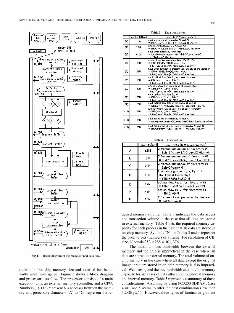
Fig. 5 Block diagram of the processor and data flow.
trade-off of on-chip memory size and external bus band-width were investigated. Figure 5 shows a block diagramand processor data flow. The processor consists of a mainexecution unit, an external memory controller, and a CPU.Numbers (1)–(12) represent bus accesses between the mem-ory and processor; characters “A” to “G” represent the re-
Table 3 Data transaction.
Table 4 Data volume.
quired memory volume. Table 3 indicates the data accessand transaction volume in the case that all data are storedin external memory. Table 4 lists the required memory ca-pacity for each process in the case that all data are stored inon-chip memory. Symbols “N” in Tables 3 and 4 representthe pixel (8 bits) numbers of a frame. For resolution of CIFsize, N equals 352 × 288 = 101, 376.
The maximum bus bandwidth between the externalmemory and the chip is impractical in the case where alldata are stored in external memory. The total volume of on-chip memory in the case where all data except the originalimage input are stored in on-chip memory is also impracti-cal. We investigated the bus bandwidth and on-chip memorycapacity for six cases of data allocation to external memoryand internal memory. Table 5 represents a summary of thoseconsiderations. Assuming by using PC3200 SDRAM, Case4 or Case 5 seems to offer the best combination (less than3.2 GByte/s). However, three types of luminance gradient

234IEICE TRANS. ELECTRON., VOL.E89–C, NO.3 MARCH 2006
Table 5 Data allocation trade-off.
(Ex, Ey, Et) used for optical flow calculation are divided toon-chip memory and external memory. Thereby, data con-trol is too complicated. Case 6 is another architecture can-didate, but 3.7 GBytes/s of band-width is too large for prac-tical implementation. In fact Case 3 was selected as the bestcandidate for the proposed architecture because it offers thelowest bus bandwidth along with a simple data control solu-tion.
3.2 Common Processor Architecture
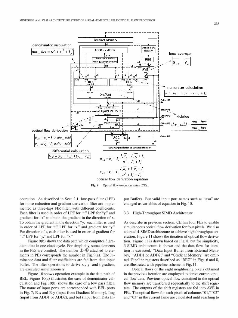
As described in a previous section, the iterated optical flowcalculation is the major workload to derive optical flowwhile other operation loads are smaller. For that reason,most hardware aside from that used for optical flow calcu-lation, is unused most of the time. The trade-off betweenoperation cycle and hardware cost was considered hence,a processor with shared operation elements was designedfor all necessary process to minimize hardware. The pro-cessor is based on the design for optical flow calculation –the heaviest operation. Other operations are realized withidentical elements by additional data path. Figure 6 showsthe proposed common execution element (CE) to realizehigh throughput operation for optical flow calculation. TheCE comprises four common processor elements (PE), twoadders for hierarchical image creation, and an accumulatorto accumulate amount of update of optical flow.
Figure 7 shows a block diagram of a PE that com-prises six blocks: an average operation block (AVE) whichexecutes average, addition and shift operations, a base ele-ment block left (BEL) and a base element block right (BER)which calculates sum of products filter, a divide or add block(Div Add), an update and low-pass filter block (Upd LPF)which operates inner product computation, and a differen-tial block (Diff) which computes subtraction and filter oper-ations.
The CE allows execution of all necessary operationsby programmable data-paths that are implemented for eachblock in the PE. Data-paths are structured to achieve high-
Fig. 6 Common execution element (CE).
Fig. 7 Common processor element (PE).
throughput operation. Figure 8 shows how optical flow op-erations are performed in the CE. The AVE block calculatesthe local average. The BEL and BER blocks derive the de-nominator and numerator, respectively. The Div Add blockcalculates division. Finally optical flow is derived throughthe Upd LPF block. The Diff block calculates amount ofupdate for all of pixel which are accumulated at ACC blockto determine whether to finish iteration.
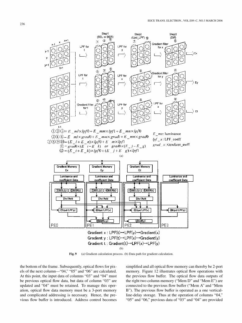
Figure 9(a) shows process flow of luminance gradient
MINEGISHI et al.: VLSI ARCHITECTURE STUDY OF A REAL-TIME SCALABLE OPTICAL FLOW PROCESSOR235
Fig. 8 Optical flow execution status (CE).
operation. As described in Sect. 2.1, low-pass filter (LPF)for noise reduction and gradient derivation filter are imple-mented as three-taps FIR filter, with different coefficients.Each filter is used in order of LPF for “t,” LPF for “y,” andgradient for “x” to obtain the gradient in the direction of x.To obtain the gradient in the direction “y,” each filter is usedin order of LPF for “t,” LPF for “x,” and gradient for “y.”For direction of t, each filter is used in order of gradient for“t,” LPF for “y,” and LPF for “x.”
Figure 9(b) shows the data path which computes 3 gra-dient data in one clock cycle. For simplicity, some elementsin the PEs are omitted. The number 1©–12© attached to ele-ments in PEs corresponds the number in Fig. 9(a). The lu-minance data and filter coefficients are fed from data inputbuffer. The filter operations to derive x-, y- and t-gradientare executed simultaneously.
Figure 10 shows operation example in the data path ofBEL. Figure 10(a) illustrates the case of denominator cal-culation and Fig. 10(b) shows the case of a low pass filter.The name of input ports are corresponded with BEL portsin Fig. 7; E x and E y (input from Gradient Memory), Img(input from ADD1 or ADD2), and buf (input from Data In-
put Buffer). But valid input port names such as “axa” arechanged as variables of equation in Fig. 10.
3.3 High-Throughput SIMD Architecture
As describe in previous section, CE has four PEs to enablesimultaneous optical flow derivation for four pixels. We alsoadopted 4-SIMD architecture to achieve high throughput op-eration. Figure 11 shows the iteration of optical flow deriva-tion. Figure 11 is drawn based on Fig. 8, but for simplicity,3-SIMD architecture is shown and the data flow for itera-tion is extracted. “Data Input Buffer from External Mem-ory,” “ADD1 or ADD2,” and “Gradient Memory” are omit-ted. Pipeline registers described as “REG” in Figs. 6 and 8,are illustrated with pipeline scheme in Fig. 11.
Optical flows of the eight neighboring pixels obtainedin the previous iteration are employed to derive current opti-cal flow data. Previous optical flow contained in the opticalflow memory are transferred sequentially to the shift regis-ters. The outputs of the shift registers are fed into AVE inPEs. The optical flows for each pixels of columns “01,” “02”and “03” in the current fame are calculated until reaching to
236IEICE TRANS. ELECTRON., VOL.E89–C, NO.3 MARCH 2006
(a)
(b)
Fig. 9 (a) Gradient calculation process. (b) Data path for gradient calculation.
the bottom of the frame. Subsequently, optical flows for pix-els of the next column—“04,” “05” and “06” are calculated.At this point, the input data of columns “03” and “04” mustbe previous optical flow data, but data of column “03” areupdated and “04” must be retained. To manage this oper-ation, optical flow data memory must be a 3-port memoryand complicated addressing is necessary. Hence, the pre-vious flow buffer is introduced. Address control becomes
simplified and all optical flow memory can thereby be 2-portmemory. Figure 12 illustrates optical flow operations withthe previous flow buffer. The optical flow data outputs ofthe right two column memory (“Mem D” and “Mem E”) areconnected to the previous flow buffer (“Mem A” and “MemB”). The previous flow buffer is operated as a one vertical-line-delay storage. Thus at the operation of columns “04,”“05” and “06,” previous data of “03” and “04” are provided

MINEGISHI et al.: VLSI ARCHITECTURE STUDY OF A REAL-TIME SCALABLE OPTICAL FLOW PROCESSOR237
(a)
(b)
Fig. 10 (a) Data path of BEL for denominator calculation. (b) Data path of BEL for LPF.
from the previous flow buffer.
3.4 Scalable Processor Architecture
One CE can perform 450 iterated calculations for CIF 30 fr/s
video. But more iterations might be required for higher ac-curacy or higher resolution. Consequently, a scalable pro-cessor architecture is necessary to meet requirements forhigher iteration. Figure 13 shows how two CEs are con-nected to double iterations. By connecting two CEs, simul-

238IEICE TRANS. ELECTRON., VOL.E89–C, NO.3 MARCH 2006
Fig. 11 Optical flow data flow with SIMD architecture.
taneous eight-pixel optical flow calculation is achievable.As described in Sect. 3.3, optical flows of the two right edgecolumns are contained in the previous flow buffer. In thiscase, the flows of the two right-most columns of CE1 areconnected with the previous flow buffer.
The optical flow derivation for the NTSC resolutionvideo is achievable using a four-CE structure. Figure 14shows a frame division scheme by four CEs (0, 1, 2, 3).By dividing optical flow derivation for horizontal pixels, thesize of optical flow memory and gradient memory of respec-tive CEs are unchanged even if the vertical pixel size is in-creased.
3.5 Design of Optical Flow Memory
As described in Sect. 3.1, large capacity buffers are requiredto achieve real-time optical flow operation. However, theprocessor core size is intended for practical use. Optical
Fig. 12 Optical flow operation using previous flow buffer.
flow derivation is an iteration of identical operations and thesame memory address is accessed repeatedly within a con-stant time interval. For that reason, SRAM is not neededfor optical flow memory. It can be a DRAM with smallerarea. Therefore, an on-chip 2-port DRAM was designed asoptical flow memory. A 2-port SRAM cell employs eighttransistors and occupies 3.79 µm2, assuming 90 nm CMOStechnology. Our proposed DRAM cell, however, achieves2-port memory function with four transistors and the areaof the memory cell is 2.13 µm2. Figure 15 shows a circuitdiagram of the DRAM cell. The CMOS configuration ofthe write- access- gate enlarges a low-voltage margin. TheDRAM cell can retain data within the iteration interval. Theinterval time of optical flow calculation is 149 µs. By ap-plying back-bias voltage, the leakage current is suppressedso that data are retained for over 200 µs at a 100◦C condi-tion, which is longer than the optical flow calculation inter-val time.

MINEGISHI et al.: VLSI ARCHITECTURE STUDY OF A REAL-TIME SCALABLE OPTICAL FLOW PROCESSOR239
Fig. 13 Scalable processor architecture.
Fig. 14 Frame division by multiple processors.
Fig. 15 Circuit diagram of 2-port DRAM cell.
3.6 Estimation of Processor Core Size
The core size of optical processor was estimated with 90-nmCMOS process technology. Figure 16 shows floor plans of:(a) optical flow memory, (b) previous buffer flow memory,and (c) luminance gradient memory. Figure 17 shows thefloor plan of the overall processor core. The floor plans aredrawn on the basis of the area estimation for each circuitblock. The estimated core size is 6.02 mm × 5.33 mm.
Table 6 shows comparison of circuit volume, mem-ory capacity, performance and accuracy between previousworks and proposed processor. The proposed processor hasachieved best performance (CIF 30 fr/s) and best accuracy(MAE=7.44) with 100% density along with relatively lowerlogic circuit volume. The proposed processor adopts origi-nal on-chip memory implementation suitable for HOE algo-rithm which described as Sect. 2.
The power consumption is 190 mW for logic, 230 mWfor DRAM and 80 mW for SRAM. Totally 500 mW is dissi-pated for CIF resolution video at frame rate 30 fr/s.
4. Conclusion
This study proposed an real-time optical flow processor ar-chitecture. That allows real-time operation with CIF 30 fr/s.Based on Hierarchical Optical flow Estimation (HOE), the

240IEICE TRANS. ELECTRON., VOL.E89–C, NO.3 MARCH 2006
Table 6 Comparison of proposed processor and previous works.
Fig. 16 Memory floor plan.
Fig. 17 Processor core floorplan.
appropriate bit-length of variables in the algorithm was de-termined while maintaining high accuracy (MAE=7.44 de-gree MAE). The proposed processor architecture achievesCIF 30 fr/s with 450 iterations. As a result of bus band widthanalysis, the optical flow memory and luminance gradient
memory were implemented as on-chip memory to realizereal-time operation. We proposed a common processing el-ement that facilitates all necessary optical flow operationsand an on-chip DRAM that can keep data within the opti-cal flow data interval time. Hence, we achieved an exten-sive reduction of silicon area. Moreover the scalable archi-tecture has been developed to meet requirements of largerframe size and higher accuracy. The processor core sizeis estimated as 6.02 mm × 5.33 mm with six-layer-metal 90-nm CMOS technology. The required operating frequencyis 189 MHz and power consumption is 500 mW with CIFresolution at frame rate 30 fr/s.
Acknowledgements
This work is supported by Semiconductor Technology Aca-demic Research Center (STARC), VLSI Design and Educa-tion Center (VDEC), the University of Tokyo in collabora-tion with Cadence Design Systems, Inc. and Synopsys, Inc.
References
[1] T. Yamamoto, K. Imamura, and H. Hashimoto, “Improvement ofoptical flow by moving-object detection using temporal correlation,”Trans. IIITE, vol.55, no.6, pp.907–911, 2001.
[2] P.H. Batavia, D.A. Pomerleau, and C.E. Thorpe, “Overtaking vehi-cle detection using implicit optical flow,” Proc. ITSC, pp.729–734,Nov. 1997.
[3] M. Tistarelli, F. Guarnotta, D. Rizzieri, and F. Tarocchi, “Applica-tion of optical flow for automated overtaking control,” Proc. IEEEWorkshop on Applications of Computer Vision, pp.105–112, Dec.1994.
[4] A. Giachetti, M. Campani, R. Sanni, and A. Succi, “The recoveryof optical flow for intelligent cruise control,” Proc. IEEE IntelligentVehicle Symposium, pp.91–96, Oct. 1994.
[5] J. Diaz, E. Ros, S. Mota, F. Pelay, and E.M. Ortigosa, “Real-time op-tical flow computation using FPGAs,” Early Cognitive Vision Work-shop, Talk21, 2004.
[6] P. Cobos and F. Monasterio, “FPGA implementation of the Horn& Schunck optical flow algorithm for motion detection in real timeimages,” Proc. DCIS’98 XIII, pp.616–621, 1998.
[7] T. Rowekamp, M. Platzner, and L. Peters, “Specialized architecturesfor optical flow computation: A performance comparison of ASIC,DSP, and multi-DSP,” Proc. ICSPAT’97, pp.829–833, 1997.
[8] P. Cobos and F. Monasterio, “FPGA implementation of camus corre-lation optical flow algorithm for real time images,” Vision InterfaceProceedings VI2001, 14th International Conference on Vision Inter-face, pp.7–9, 2001.
[9] A. Zuloaga, J.L. Martin, and J. Ezquerra, “Hardware architecture foroptical flow estimation in real time,” Proc. International Conferenceon Image Processing, ICIP 98, vol.3, pp.972–976, 1998.
[10] M.V. Correia and A.C. Campilho, “Real-time implementation of anoptical flow algorithm,” ICPR, vol.4, pp.247–250, 2002.

MINEGISHI et al.: VLSI ARCHITECTURE STUDY OF A REAL-TIME SCALABLE OPTICAL FLOW PROCESSOR241
[11] B.K.P. Horn and B.G. Schunck, “Determining optical flow,” AI,vol.17, pp.185–204, 1981.
[12] B. Lucas and T. Kanade, “An iterative image registration techniquewith an application to stereo vision,” Proc. DARPA Image Under-standing Workshop, pp.121–130, 1981.
[13] S. Uras, F. Girosi, A. Verri, and V. Torre, “A computational approachto motion perception,” Biol. Cybern., vol.60, pp.79–97, 1988.
[14] H.H. Nagel, “On the estimation of optical flow: Relations betweendifferent approaches and some new results,” AI, vol.33, pp.299–324,1987.
[15] P. Anandan, “A computational framework and an algorithm for themeasurement of visual motion,” Int. J. Comput. Vis., vol.2, pp.283–310, 1989.
[16] A. Singh, “An estimation-theoretic framework for image-flow com-putation,” Proc. IEEE ICCV, pp.168–177, Osaka, 1990.
[17] D.J. Fleet and A.D. Jepson, “Computation of component image ve-locity from local phase information,” Int. J. Comput. Vis., vol.5,pp.77–104, 1990.
[18] E.P. Simonceli, “Design of multi-dimensional derivative filters,”Proc. First IEEE Int. Conf. Image Processing, vol.I, pp.790–794,1994.
[19] P. Anandan, J.R. Bergen, K.J. Janna, and R. Hingorani, “Hierarchi-cal model-based motion estimation,” in Motion Analysis and ImageSequence Processing, ed. M.I. Sezan and R.L. Lagendijk, pp.1–22,Kluwer, Boston, MA, 1993.
[20] S.H. Hwang and S.U. Lee, “A hierarchical optical flow estimation al-gorithm based on the interlevel motion smoothness constraint,” Pat-tern Recognit., vol.26, no.6, pp.939–952, 1993.
[21] J.L. Barron, D.L. Fleet, and S.S. Beauchemin, “Performance of op-tical flow techniques,” Int. J. Comput. Vis., vol.12, no.1, pp.43–77,1994.
Noriyuki Minegishi graduated from ToinTechnical College in 1985. He joined Mit-subishi Electric Corp. in 1985, where he hasbeen engaged in video processing, chip design,and verification of video processing. He is amember of the Information Technology R&DCenter (Kamakura, Japan). From 2003, he isalso enrolling in the Doctoral course of Kana-zawa University.
Junichi Miyakoshi received a B.E. degreefrom Kanazawa University in 2002. He receivedan M.S. from Kanazawa University in 2004. Heis currently enrolled in the Doctoral course ofKobe University. His research focus is low-power VLSI techniques for image processing.
Yuki Kuroda received a B.E. degree andM.S. in Electrical and Information Engineeringfrom Kanazawa University, Ishikawa, Japan, in2003 and 2005 respectively. He joined HitachiLtd., Central Research Laboratory where he hasbeen engaged in low-power design technologyand multimedia processing for mobile commu-nications and intelligent transport systems.
Tadayoshi Katagiri was born on Febru-ary 23, 1982. He received a B.E. in Informa-tion and Systems Engineering from KanazawaUniversity in 2004. He is currently pursing aMaster’s degree at Kanazawa University. Hisresearch interests are video segmentation algo-rithms based on optical flow techniques.
Yuki Fukuyama was born on March 15,1982. He received a B.E. in Computer andSystems Engineering from Kobe University in2005. He is currently a Master’s student at KobeUniversity. His research interest is low-powerVLSI techniques for image processing.
Ryo Yamamoto was born on April 26,1982. He received a B.E. in Electrical and Infor-mation Engineering from Kanazawa University,Ishikawa, Japan, in 2005. He is currently a Mas-ter’s student at Kobe University. His research in-terest is low-power VLSI system for image pro-cessing.
Masayuki Miyama was born on March26, 1966. He received a B.S. in Computer Sci-ence from the University of Tsukuba in 1988.He joined PFU Ltd. in 1988. He received anM.S. in Computer Science from the Japan Ad-vanced Institute of Science and Technology in1995. He joined Innotech Corp. in 1996. Hereceived a Ph.D. in Electrical Engineering andComputer Science from Kanazawa University in2004. He is a Research Assistant in the Depart-ment of Electrical and Electronic Engineering at
Kanazawa University. His present research focus is a low-power designtechnique for multimedia VLSI.
242IEICE TRANS. ELECTRON., VOL.E89–C, NO.3 MARCH 2006
Kousuke Imamura received B.S., M.S.and Dr. Eng. degrees in Electrical Engineeringand Computer Science in 1995, 1997 and 2000,respectively—all from Nagasaki University. Heis currently a Lecturer of Information and Sys-tems Engineering, Kanazawa University. His re-search interests are high-efficiency image cod-ing and image processing.
Hideo Hashimoto received the B.S., M.S.and Dr. Eng. degrees in Electronic Engineeringin 1968, 1970 and 1975, respectively, all fromOsaka University. He joined Electrical Commu-nication Laboratories of Nippon Telegraph andTelephone Corporation (NTT) in 1975. Since1993, he has been a professor of Informationand System Engineering, Kanazawa University.His research interests are video coding, movingobject segmentation and visual communication.
Masahiko Yoshimoto received a B.S. inElectronic Engineering from the Nagoya Insti-tute of Technology, Nagoya, Japan, in 1975, andan M.S. degree in Electronic Engineering fromNagoya University, Nagoya, Japan, in 1977. Hereceived a Ph.D. in Electrical Engineering fromNagoya University, Nagoya, Japan in 1998. Hejoined the LSI Laboratory, Mitsubishi ElectricCorp. Itami, Japan, in April 1977. From 1978to 1983, he was engaged in the design of NMOSand CMOS static RAM, including a 64-Kb full
CMOS RAM with a divided-word-line structure. Since 1984 he has beeninvolved in research and development of multimedia ULSI systems for dig-ital broadcasting and digital communication systems based on MPEG-2 andMPEG-4 Codec LSI core technology. Since 2000, he had been a Professorof the Dept. of Electrical & Electronic System Engineering at KanazawaUniversity, Japan. Since 2004, he has been a Professor of the Dept. ofComputer and Systems Engineering in Kobe University, Japan. His currentactivities are centered upon the research and development of multimediaand ubiquitous media VLSI systems including an ultra-low-power imagecompression processor and a low-power wireless interface circuit. He holds70 registered patents. Dr. Masahiko Yoshimoto is a member of the IEEE.He served on the Program Committee of the IEEE International Solid StateCircuit Conference from 1991 to 1993. In addition, he has served as GuestEditor for special issues on Low-Power System LSI, IP and Related Tech-nologies of IEICE Transactions in 2004. He received the R&D100 awardsfrom the R&D magazine for development of a DISP and the developmentof a real-time MPEG-2 video encoder chipset in 1990 and 1996, respec-tively.