vol. 43, no. 1/2 - plasma processing high-density...
TRANSCRIPT

High-density chemical vapour deposition ... IBM J. of Res. & Dev., 43(1/2), 1999. 1
Vol. 43, No. 1/2 - Plasma processing 0018-8646/99/$5.00 © 1999 IBM
High-density plasma chemical vapor deposition of silicon-based dielectric films for integrated circuits
by S. V. Nguyen
In this paper, we present and review recent developments in the high-density plasma chemicalvapor deposition (HDP CVD) of silicon-based dielectric films, and of films of recent interest inthe development of lower-dielectric-constant alternatives. Aspects relevant to the HDP CVDprocess and using the process to achieve interlevel insulation, gap filling, and planarizationare discussed. Results obtained thus far suggest that the process may play an important role
in the future fabrication of integrated circuits, provided several metal-contamination andprocess-integration concerns can be effectively addressed.
Introduction
The chemical vapor deposition (CVD) of undoped and doped silicon-based dielectric layers plays akey role in the microelectronics technology. To advance the dielectric-layer-related aspects of thetechnology, facilitating its evolution beyond its current level of integration, advanced, low-temperature CVD processes will be needed. The processes should produce dielectric layers withminimal substrate heating (preferably lowering the "thermal budget"), have no deleterious effectson underlying gate oxides and other device structures, be suitable for filling sub-half-micron high-aspect-ratio device and circuit structures, and have reflow characteristics that facilitate the use ofthe chemical-mechanical polishing (CMP) used to achieve planarization. Additionally, they shouldrequire fewer process steps, thereby reducing overall fabrication costs [1].
At present, Al(Cu)-based conductor films and silicon oxide dielectric films deposited by CVD areused to produce most of the interconnections on multilevel integrated-circuit chips. To facilitate theevolution to higher levels of performance, a significant next step is underway: replacement of theAl(Cu)- based conductors with lower-resistance Cu-based conductors (see for example [2, 3]). Thischange reduces the RC interconnection delay significantly--by a factor of about 1.5. At present, itappears that to achieve a further significant reduction, it will be necessary to reduce the dielectricconstant k of the dielectric films. It is estimated that the delay could be reduced by a factor of about3 if the silicon oxide films, which have a dielectric constant of around 4, could be replaced by filmshaving a dielectric constant of 2 [3]. There is, however, no clear indication of what approach shouldbe used to achieve a reduction in k. One approach, leading to a small reduction (to a value of 3.3-3.5), involves the incorporation of a small amount of bonded fluorine in silicon oxide filmsdeposited by HDP CVD to form a fluorinated oxide. The approach, discussed in detail in this paper,should require only a minimal change in integrated-circuit fabrication [3-7]. Other approaches,leading to a reduction of k to 2-3, involve the use of films such as carbon-doped silicon oxide [8, 9],and carbon and fluorinated carbon [10-16], deposited by either CVD or HDP CVD.
Many recent publications discuss various types of HDP sources [17, 18] and their use for dielectricfilm deposition and gap filling [19-34]. Electron cyclotron resonance (ECR) [19-24], helicon,helicon resonator [25, 26], and ICP sources [7, 13, 29-35] have been used for CVD processdevelopment and in early pilot line manufacturing with promising results. In submicron devicefabrication, interlevel dielectric gap filling (or, simply, "gap fill") of high-aspect-ratio (>1.2)
High-density chemical vapour deposition ... IBM J. of Res. & Dev., 43(1/2), 1999. 2
topography generally requires the use of multistep deposition/etch or spin-on dielectric processingto produce void-free, filled structures [1]. With HDP CVD processing, high-aspect-ratio (up to 4:1)sub-half-micron structures can be filled and locally planarized in a single processing step.Generally, the ions and electrons from the plasma are generated at an electrode by means of an rfpower source, and an rf biasing power source is applied to another (wafer-holding) electrode tocreate a significant ion bombardment (sputter-etching) component during deposition. For gapfilling, HDP CVD processing is thus a simultaneous deposition/etching process in which looselydeposited films, or "deposited species," over planar or topographical surfaces are sputtered off byreactive ions and radicals during deposition [29, 32, 34]. The deposition/sputtering-rate ratio (D/S)is an important measure of the gap-filling capability of the processes. This ratio is defined as
D/S=(net deposition rate+ blanket sputtering rate)/blanket sputtering rate.
In general, the use of a lower D/S ratio facilitates the filling of a structure with a higher aspect ratio,but at a lower deposition rate.
Several commercial high-density plasma CVD systems [32, 35, 36] have been developed inconnection with efforts to advance the integrated-circuit technology to the ULSI (ultralarge-scaleintegration) level. These systems use either ECR or ICP sources for high-density plasma generation.The advantages of each type of plasma source have recently been a subject of extensive discussionsand are not covered here. Readers interested in these plasma sources, which are used in depositionand etching, may obtain more detail from recent publications [17, 18]. Since the commercial ECRsystem has been available for almost ten years, and deposited films and processes have been studiedextensively by this author and many others [19-22, 36-38], we do not discuss additional ECR CVDresults here. In this paper, the emphasis is on recent results obtained for low-temperature HDP CVDof silicon oxide and fluorinated (fluorine-doped) silicon oxide dielectric films, deposited incommercially available inductively coupled plasma (ICP) HDP CVD systems. Results for low-kdielectrics such as carbon and fluorocarbon deposited by HDP CVD processing are also discussed.The promising results obtained lead us to believe that HDP CVD processing may become importantin the future fabrication of integrated circuits.
HDP CVD processing and equipment aspects
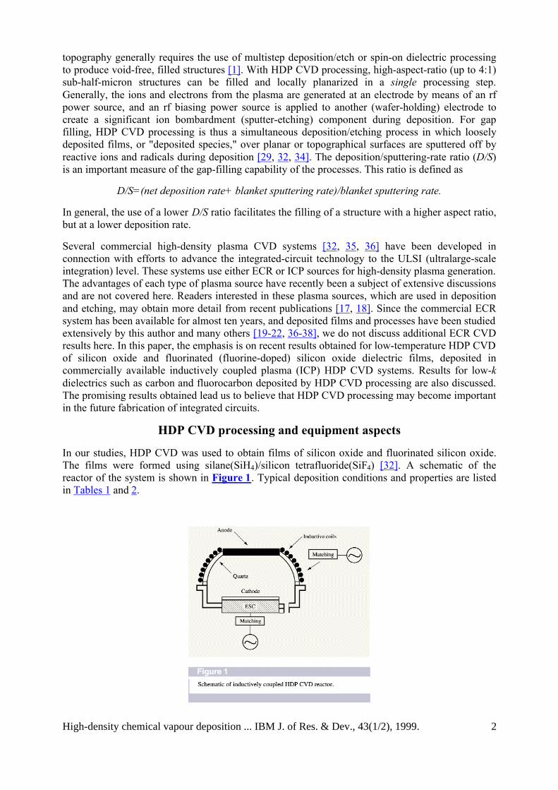
In our studies, HDP CVD was used to obtain films of silicon oxide and fluorinated silicon oxide.The films were formed using silane(SiH4)/silicon tetrafluoride(SiF4) [32]. A schematic of thereactor of the system is shown in Figure 1. Typical deposition conditions and properties are listedin Tables 1 and 2.

High-density chemical vapour deposition ... IBM J. of Res. & Dev., 43(1/2), 1999. 3
Table 1 Typical deposition conditions and properties of silicon oxide films deposited using HDP CVD.
Deposition processparameters
Value
Source rf power range 2000-4000 WGases SiH4/Ar/O2 = 32-45/0-40/43-60 sccmPressure <5 mTorrDeposition/sputtered ratio 3.2:1 (filled 0.25 µm, 2.5:1 aspect ratio structure)Deposition temperature 250-350°CDeposition rate 180-400 nm/minRefractive index 1.46 ± 0.003Film stress (0.7 µm, 25°C) (-)1.0-1.6 x 10⁹ dynes/cm2
Wet-etching rate(6:1 buffered HF) 1.6-1.8 x that of thermally grown oxide
Table 2 Typical deposition conditions and properties of fluorinated silicon oxide films deposited using HDP CVD.
Deposition processparameters
Value
Source rf power range 1000-4000 WGases SiH4/SiF4/Ar/O2=0-34/0-34/0-20/47-60 sccmPressure <4 mTorrDeposition/sputtered ratio 3.2:1 (filled 0.25 µm, >3:1 aspect ratio structure)Deposition temperature 300-375°CDeposition rate 130-300 nm/minRefractive index rangs 1.43-1.47Film stress (0.7 µm, 25°C) (-)1.0-1.6 x 10⁹ dynes/cm2
Wet-etching rate (6:1 buffered HF) 1.5-1.9 x that of thermally grown oxideCMP rate (oxide slurry) 1100 Å/min (1.05 x that of plasma CVD oxide)
The HDP CVD process requires the use of a relatively low pressure (2-10-mTorr range) to achievea high electron density (1010 -1012 cm3) and a high fractional ionization rate (10-4 to 10-1). Because ahigh film-deposition rate is required for practical applications, simple initial reactant gases such assilane, silicon tetrafluoride, and oxygen are used. Complex organosilicon reactants such astetraorthosilicate (TEOS) that are normally used in conformal plasma CVD processes [39] aredissociated into many fragmented reactive species in an HDP CVD system, increasing depositionsystem pressure significantly while offering little or no advantage. In order to achieve a significantdeposition rate while maintaining a reasonably high sputter-etching rate for gap-filling purposes, asignificant amount of initial reactant (i.e., deposited species in the plasma) must flow through thereactor, but the system must be kept at low pressure constantly during deposition. As a result, therequired vacuum system must have a high pumping capability throughput and robustness: It mustwithstand the high temperature and high reactivity of the reaction by-products while removing themat a high rate. For an HDP CVD system, an advanced turbomolecular pump is generally required toachieve a suitable deposition rate (at low pressure) and acceptable pumping reliability [40]. Thevacuum pump system is a part of the HDP CVD process that currently requires more attention.
As already noted, the HDP CVD of silicon oxide, especially under high rf biasing gap-fillconditions, produces concurrent deposition and etching. The etching and the (exothermic) siliconoxide deposition reactions each generate a large amount of heat that must be removed from thesubstrate during processing. For both Al-based and Cu-based sub-half-micron metal interconnects,temperature increases to above 400°C may cause significant reliability problems. For example, attemperatures above 450°C, Al-based conductors may actually start to melt. A uniform temperatureacross a wafer during processing is required to ensure homogenous film composition and propertiesover its entire area. Therefore, a major aspect of HDP CVD processing is the monitoring and

High-density chemical vapour deposition ... IBM J. of Res. & Dev., 43(1/2), 1999. 4
maintenance of substrate temperature. The mechanical clamp that is commonly used to retainwafers during processing would not meet the stricter requirements of heat-transfer uniformity andlow particulate generation for ULSI fabrication, and would contribute to wafer bowing.Furthermore, the mechanical clamp also interferes with the plasma distribution and the gas flow,acting like a heat sink and thus possibly reducing overall process uniformity. Wafer clampingwithout topside contact would provide advantages regarding the reduction of particle generationand reduction of wafer-edge exclusion area (thus facilitating the fabrication of more chips on awafer). Significant work has been done to develop various types of electrostatic wafer clamping forULSI manufacturing [41-43]. Three configurations of interest are the unipolar, bipolar, andJohnsen-Rahbek configurations. The optimal design, configuration, fabrication materials, andprocess details of the configurations are closely kept secrets, with little information available [41,42]. The HDP CVD process, with its relatively high-temperature sputter-etching and ionbombardment, requires the use of high-purity ceramic material for chuck coatings in order toeffectively reduce contamination. Other high-purity ceramic, metal oxide, and other materials suchas sapphire (single-crystal Al2O3) are also being explored for that purpose [44].
In all commercial HDP CVD equipment in current use, there is no heating element in the depositionreactor. Wafer heating is normally initiated with an Ar plasma after the wafer is loaded into thereaction chamber. After the wafer reaches the desirable temperature, which is normally in the 300-400°C range, other reactant gases are introduced to produce film deposition. Depending on theconfiguration of the plasma reactor and the type of wafer used, many process parameter sequencescan be modified during deposition to minimize both electrical and physical damage to thetopography and electronic features on the wafer [45, 46], especially on the step corner of depositingsurface features. Since production is normally implemented in a batch of 25 wafers, the argonplasma is sometimes kept on constantly between runs to maintain a baseline temperature in thedeposition reactor. For both silicon oxide and fluorinated silicon oxide gap-fill film-depositionprocesses, a gradual ramping up of rf bias minimizes physical and electrical damage. Furthermore,gradual ramping up will reduce an initial rf power surge during the initial transient phenomena ofplasma-enhanced CVD processing [47, 48] that may also cause unexpected damage to devices. Fordeposition processes, involving volatile etching reactants such as fluorines, as in the case offluorine-doped oxide film deposition, the etching component of the HDP CVD gap-fill processbecomes significant, and the rf biasing power must be reduced, compared to the case for undopedsilicon oxide, in order to prevent step corner erosion.
We have used analysis techniques such as Fourier transform infrared resonance (FTIR), Auger,secondary ion mass spectroscopy (SIMS), and nuclear reaction analysis for hydrogen [49] toanalyze the film's bonding structures and composition. A Perkin-Elmer 1725X FTIR system wasused to analyze the films, as described in our recent publication [50]. Auger analysis was performedon a Perkin-Elmer Model 650 scanning auger microscope with a beam voltage of 5 kV and anapproximate current of 100 nA (rastered 100-µm spot size). Other film properties such as stress,wet etching, and CMP rate in conventional oxide slurry were also evaluated.
Complex multilevel 0.20-0.25-µm STI, GC, and IMD structures with high aspect ratios (1.5-3.5)were filled with HDP CVD undoped silicon oxide. In the case of IMD structures, lower dcfluorinated silicon oxide films were also used for the gap-fill deposition. These structures weresubsequently processed to several metal levels and then evaluated for dielectric gap fill, CMPintegration, and plasma damage on 80-100-Å gate-oxide devices. The results were compared tothose for the same device structures processed with conventional LPCVD SiO2 or plasma CVDoxide gap-fill processing.
Plasma-CVD-induced damage was also measured using the antenna structures as dielectric test site(DTS) monitors containing large-area polysilicon capacitors and antenna devices with areas rangingfrom 0.2 to 0.001 cm2. The antenna ratio is defined as the ratio of the polysilicon gate area to the
High-density chemical vapour deposition ... IBM J. of Res. & Dev., 43(1/2), 1999. 5
thin gate-oxide area. The antenna devices on DTS monitor wafers have ratios of 0.2, 1, and 10 M(million). The higher the antenna ratio, the more sensitive the devices are to plasma damage. Detailsof the fabrication process and structure of these DTS monitors have recently been presented [51].Intra and inter-level dielectric constants have also been measured using fingered comb structureswith spacings ranging from 0.50 to 10 µm, as described in a previous publication [52]. The resultswere also confirmed with 0.25-µm Al(Cu) interconnect patterned test structures.
Deposited film characterization and properties
• Undoped silicon oxide films
Silicon oxide films were deposited using a silane/oxygen/argon gas mixture. Besides parametersassociated with the design of the system, the inductive coil, and the plasma source, there are severalprincipal process parameters that affect the deposited film properties: substrate temperature,reactant gas ratio, rf biasing power, and deposition pressure. FTIR analysis showed that filmsdeposited under the conditions of Table 1, with high oxygen/silane ratios, display no waterabsorption and a small amount of O-H bonding (3674 cm-1), as indicated in Figure 2. The Si-Ostretching band (1085 cm-1) half-peak- width maximum is typically small (88 cm-1). The indicatedHDP CVD film bonding features are similar to those of conventional high-temperature LPCVDSiO2 films deposited at 650-700°C. These HDP CVD films also display uniform and stoichiometricsilicon dioxide compositions and hydrogen concentrations typically ranging from 1.5 to 2.0 atomicpercent (at.%) depending on deposition conditions.
Typical Auger electron spectroscopy (AES) and hydrogen depth profiles are shown in Figures 3and 4, respectively. The Auger depth profile composition is highly uniform, indicating a goodprocess control. Wet etching in buffered HF solution (6:1 of water:buffered HF) indicated less thana ±5% variation in etching rate with depth and across a 200-mm-diameter wafer. The wet-etchingrate in this solution is about 1.6-1.8 times that of thermally (950°C) grown oxide films. It should benoted that conventional plasma CVD films have a wet-etching-rate ratio of 1.7 to 2.0 compared tothat of thermally grown oxide. These results confirm that films of improved quality and consistencycan be deposited by HDP CVD.
Films deposited with a higher rf bias power and temperature range (Table 1) display a denserbonding structure and lower hydrogen content. The denser bonding structure is indicated by a moregradual Auger depth profile, slightly less Si-O HPWM bonding, and a lower buffered HF wet-etching rate at similar stoichiometric SiOx compositions. Films deposited with a high oxygen/silaneflow ratio (oxygen-rich region) display a refractive index near 1.46 and uniform silicon and oxygenstoichiometric SiO2 profiles.
During the first few silicon oxide deposition runs on blanket silicon wafers, SIMS analysis showedno significant metal contamination (<1 x 1015 cm-3) in deposited films. However, after theequipment was used to deposit films on ILD wafers with Al(Cu)-based metallization patterns, SIMSanalysis indicated some aluminum contamination in the 1 x 1016-cm-3 range and some Cr at Siinterfaces but with no significant carbon, iron, copper, or nickel contamination (Figure 5).Therefore, the Al contamination may have arisen from the Al(Cu)-based metallization on patternedwafers that was sputtered off during the initial Ar plasma heating period of the HDP CVDprocessing sequence, as discussed previously. Even for an HDP CVD system that had not beenexposed to patterned, metallized wafers, a slight increase in aluminum and other metalcontamination in the deposited films has been observed after prolonged operating periods. Suchcontamination has been traced to several equipment parts such as the inductive plasma dome andthe electrostatic chuck. During the heating and deposition process, materials such as the aluminaovercoat may be sputtering off the parts via high-energy ion sputtering, especially when high-aspect-ratio gap fill is required. Such low-level metal contamination is not an issue for ILDapplications. However, it is of considerable concern in connection with ULSI device and circuit

High-density chemical vapour deposition ... IBM J. of Res. & Dev., 43(1/2), 1999. 6
requirements, with regard to both STI and GC gap-fill applications. Even at low levels(contamination in the 1 x 1016-cm-3 range), it will degrade device performance and reliability. Thismetal contamination can be reduced by depositing a thin silicon oxide passivation film after theplasma-cleaning step. For ICP HDP CVD systems containing an alumina or silica dome withinwhich rf power is applied, the metal contamination in the material that is used to fabricate the domemay leach out into the deposition system after many hours of operation. Therefore, if the process isto be used for STI and GC gap fill, it will be necessary to carefully monitor the level of metalcontamination and devise means to reduce it to an acceptably low level (<1 x 1015 cm-3) in thedeposited films.
For HDP CVD silicon oxide films deposited with high D/S and oxygen/silane ratios (and with arefractive index in the 1.462 ± 0.002 range) that fill 0.25-2.0-µm structures with a 2:1 aspect ratio,inter- and intra-level dielectric constants are found to be 4.00 ± 0.05 using fingered comb structureswith spacings ranging from 0.50 to 10 µm [52].
Chemical-mechanical polishing (CMP) results have indicated that the CMP rate for HDP CVDoxide in a conventional oxide slurry is about 1100 Å per minute, comparable to those for plasmaCVD silane-based oxide films. A typical thickness measurement of a blanket HDP CVD oxide filmbefore and after removal of about 1300 Å of oxide by CMP showed no significant degradation infilm uniformity (Figure 6).

High-density chemical vapour deposition ... IBM J. of Res. & Dev., 43(1/2), 1999. 7
In order to study plasma-induced damage todevice structures, multilevel 0.25-µm STI, GC,and IMD structures filled with HDP CVDsilicon oxide films were examined. Resultsobtained were similar to those obtained whenuse was made of conventional thermal LPCVDprocesses. The breakdown yield was above 90%even after a 10-MV/cm field was applied to thegate-oxide films. Electrical yields of polysilicon100-Å-thick gate-oxide capacitors with 0.2, 2,and 10M:1 antenna ratios were also high(>90%). A schematic of the test structure usedis shown in Figure 7, and the results obtainedare summarized in Table 3. The HDP CVDconditions used were those listed in Table 1.The results obtained indicated that the HDPCVD processing did not cause any significantdamage to 80-100-Å- thick gate oxides undervarious processing conditions suitable for fillinghigh-aspect-ratio 0.25-µm Al(Cu)-basedinterconnect gaps. More recent data have shownthat no significant plasma damage is observedto 50-Å-thick gate oxides under similar processconditions. Overall, the gate damage caused byHDP CVD processing has been found to bemuch smaller than that from conventionalplasma CVD processing at a lower rf powerdensity.
Table 3 Electrical yields of polysilicon 100-Å-thick gate-oxide capacitors having antenna ratios of 0.2M:1, 2.0M:1,and 10M:1.
Runnumber
Conditions Yield(%)
Comments
0.2M:1 2.0M:1 10M:1 1 A 100 98 100 Good2 B 100 100 95 Good3 C 100 100 100 Best result4 D 100 98 98 Good5 E 100 100 90 OK (lowest)6 F 100 100 95 OK
ControlNo plasma
process100 100 100 OK

High-density chemical vapour deposition ... IBM J. of Res. & Dev., 43(1/2), 1999. 8
• Fluorine-doped silicon oxide films
Generally, HDP CVD fluorinated silicon oxide (hereafter referred to as "fluorinated oxide" or "F-oxide") films can be deposited by gas precursors containing SiF4/O2 or an SiF4/SiH4/O2
combination. Our recent work [6, 7, 53, 54] and that of others [55-57] has shown that the presenceof hydrogenated reactants in the gas precursors improves that stability of fluorinated oxide films.The hydrogen in the discharge appears to remove the excess fluorine and enhance the film stability.Without the hydrogen from an initial precursor suchas H2 or SiH4, the fluorinated oxide filmsgenerally display a slightly lower deposition rate and absorb water more readily than underconventional plasma CVD conditions. By using a SiF4/SiH4/ O2 precursor, relatively high fluorineconcentrations (up to 14-15 at.%) can be incorporated into the silicon oxide bonding network whilestill maintaining film stability. This stable fluorine incorporation is due to the direct insertion of Si-F bonding units, forming from SiF4 dissociation, into the Si-O bonding network. Excess fluorinefrom SiF4 dissociation is also effectively removed by excess hydrogen from SiH4 dissociation.During HDP CVD processing, as already indicated, deposition and etching occur simultaneously atthe substrate surface. The deposition species are formed from reactions between reactive species ofSiH4(2% in argon)/SiF4/O2 generated in the plasma. Fluorine etching species are produced fromSiF4 dissociation. Although the etching yield of deposited oxide films is much smaller than whenC2F6 is used [6], the etching component is still quite high under high rf and rf-biasing power levelsand/or large SiF4 flow. Under such conditions, increased ion bombardment and fluorine dissociationenhance the etching component, thus effectively reducing the deposition rate and the amount offluorine incorporated in the films.
Parametric studies of the deposition rate, refractive index, fluorine incorporation, and Si-F and Si-Obonding variations with deposition parameters [rf power (forward and bias), gas-flow ratios,substrate temperature, etc.] show that the amount of fluorine incorporation in the film is stronglyinfluenced by the SiF4/SiH4 ratio and the rf power used. The substrate heating by the initial Arplasma has a significant effect on the amount of fluorine incorporated and its stability in the films.F-oxide films deposited at a higher processing temperature (Table 2 conditions) contain lessfluorine. Under the same process conditions, the fluorine incorporation in the films increases withincreasing SiF4 flow and decreases with increasing rf bias power and inductive power. Figure 8shows a typical effect of rf biasing power on the deposition rate at three SiF4 flow ratios under theconditions of Table 2. It can be seen from the results that ion bombardment (i.e., sputtering effect)has a significant effect on the deposition rate. As in a conventional plasma CVD process, HDPCVD fluorinated oxide deposition process parameters can be changed to optimize film propertiesfor specific applications. Figure 9 shows typical FTIR spectra of F-oxide films deposited at 1 and2.5 kW of rf biasing. These spectra indicate film stability and show the presence of Si-F (945 cm-1),Si-OH (silanol, 3670 cm-1), and Si-O (460, 835, and 1130 cm-1) bonds with no water absorption.Figure 10 shows the effect of rf biasing power on the amount of silanol bonding in five films. Thedecrease with rf power may have been due to increased ion bombardment during film deposition.An increase in SiF4 flow ratio from 15 to 29% also decreased the silanol concentration. In bothcases, the hydrogen was removed either by ion bombardment or by the presence of fluorine speciesgenerated during SiF4 dissociation. It should be noted that stable F-oxide films deposited withSiF4/O2 initially contained no silanol but slowly absorbed water (hydrolyzed) upon exposure to highhumidity. The absorption was less if the films were capped by undoped oxide or the concentrationof fluorine on exposed surfaces was lower. Under our baseline conditions, HDP CVD F-oxide filmsdeposited with a greater SiF4 flow level or more rf power displayed less silanol bonding and did notabsorb water upon exposure to air ambient. Figure 11 shows typical AES depth profiles of HDPCVD F-oxide films deposited at SiF4 flow levels of 29% and 100%. It can be seen that the fluorineconcentration was lower at the film interface and surface, thus enhancing film stability. Analysisindicated a slightly lower hydrogen content in F-oxide films (0.5-1.4 at.% vs. 1-1.6 at.% for siliconoxide films), as shown in Figure 12. With regard to metal contamination, similar results wereobserved in both silicon oxide and fluorinated oxide films, as discussed previously. The wet-etching

High-density chemical vapour deposition ... IBM J. of Res. & Dev., 43(1/2), 1999. 9
rate in buffered HF and the chemical-mechanical polishing rate in an oxide slurry are indicated inTable 2. In our CMP study using blanket HDP CVD F-oxide films deposited with a SiF4 precursorand with a 5-6 at.% fluorine concentration, no significant interaction between the slurry and thefilms was observed, and the CMP rate was increased only slightly. However, it should be noted thata recent report [58] has indicated that plasma CVD F-oxide films deposited with a C2F6 precursorand with 8-9 at.% fluorine concentration show more sensitivity to CMP. CMP rates up to 30%higher were observed for F-oxide films compared to undoped films, and the rate increased withincreasing fluorine concentration. The increased CMP rate was attributed to the increasedhydrolysis of Si-F bonds in the CMP slurry solution.

High-density chemical vapour deposition ... IBM J. of Res. & Dev., 43(1/2), 1999. 10
In a recent study, we have found that F-oxide films deposited by conventional plasma CVD withsimilar precursors but without a hydrogen source [i.e., SiF4/O2 (or N2O) only] display relatively lowdeposition rates and absorb water more readily upon exposure to air [54]. With conventional plasmaCVD processing, a hydrogen source is needed to increase both film stability and deposition rate.However, in HDP CVD, where increased electron dissociation of SiF4/O2 precursors and increasedion bombardment of deposited films on the substrate occur, slightly less stable F-oxide films can bedeposited with or without the addition of a hydrogen (H2 or SiH4) precursor, but at a lowerdeposition rate and with less fluorine incorporation in the films. For HDP CVD fluorinated siliconoxide film deposition, increased ion bombardment during deposition (by increasing rf bias power)increases film stability but reduces the amount of incorporated fluorine and the deposition rate. Theconcentration of incorporated fluorine, its bonding structure, and its depth profile in the depositedfilm have significant effects on film stability. The fluorine depth profile, concentration, and bondingcan be manipulated to improve stability with suitable deposition conditions. Another study [59] hasindicated that a suitable amount of fluorine incorporation was shown to passivate and neutralize anytrapped charge existing in HDP CVD oxide films, thus increasing the film breakdown voltage.However, too much fluorine incorporation in the films results in the formation of a porous oxidenetwork and hole traps, and eventually causes device reliability problems. It is possible to modifyprocess conditions to enhance F-oxide film stability. For example, surface treatment of fluorinatedoxide films by nitrous oxide plasma exposure reduces the fluorine concentration on the film surfaceand improves adhesion by subsequently deposited films [60].
Overall, our HDP CVD oxide films deposited with SiF4/SiH4/O2 precursor chemistry appeared to bemore stable than films deposited with other fluorine precursors such as CF4 or C2F6. The enhancedstability of our fluorine-doped oxide films can also be attributed to the use of Si-F bondingprecursors [6, 53]. Precursors with Si-F bonding, such as SiF4, dissociate to form Si-F precursors inan HDP discharge. Subsequently, the Si-F species will incorporate directly at the Si-F bonding unitin the film surface without going through fluorine reactive species formation and incorporation inthe F-oxide film, as in the case of a CF4 precursor. Since the Si-F species is generated and thensubsequently bonded (incorporated) directly into the film, the overall Si-F bonding energy change islower. This is probably responsible for the enhanced film stability observed in F-oxide filmsdeposited with an Si-F precursor under various deposition conditions.
In general, the chemical aspects of plasma deposition are complex and involve many reaction steps[61], especially in HDP CVD. Furthermore, active fluorine etchant species (F, SiFx, HF, etc.) act asetching or deposition species both in the discharge chamber and on the substrate surface under asuitable selection of process parameters. However, our results and those of others [7, 54-57] suggesttwo principal mechanisms that may be used as a general guideline to obtain more stable fluorinatedoxide films: a) the insertion of more stable and direct Si-F bonding species into the films (this canbe accomplished by suitable deposition precursors with Si-F bonding [6, 7, 53]); and b) facilitatingthe removal of excess fluorine generated in the plasma discharge by including hydrogen-basedprecursors (hydrogen, silane, etc.) to form more volatile species such as H-F, and enhanced ionbombardment (by increasing HDP rf biasing power) to remove or/and to densify loosely bonded Fspecies in the film.
Stable fluorinated silicon oxide films with up to 10 at.% fluorine can be deposited for high-aspect-ratio >= 3:1) gap fill using this approach. Up to 15 at.% fluorine can also be incorporated into theoxide film using HDP processing, but these films tend to be less stable (i.e., absorb moisture uponlong-term exposure in air) than films with 5-10 at.% fluorine. The measured dielectric constants ofthe latter films are in the 3.4-3.6 range [52]. Another study [62] has predicted that the dielectricconstant of F-oxide films should be reducible to a level as low as 2.6; the prediction was based on aKramer-Kronig calculation. However, experimental electrical C-V measurements on F-oxide films

High-density chemical vapour deposition ... IBM J. of Res. & Dev., 43(1/2), 1999. 11
have failed to produce so low a value. Reported k values range from 3.1 to 3.7, depending onprocess conditions. These values are more consistent with the ab initio calculation by Lucovsky andYang [63], which showed that 10-12 at.% incorporation of fluorine in silicon oxide films shouldreduce the k value to the 3.2-3.4 range. It should be noted that both calculations do not include theeffect of -OH incorporation in the F-oxide films; that should increase the dielectric constant. Forless stable F-oxide films, the slow absorption of water vapor in air increases k with time. It shouldbe noted that in the recent report mentioned above [64], fluorinated silicon oxide was used as a low-k dielectric material for fabricating multilevel logic devices.
• General properties of carbon- and fluorine-doped carbon films*
As mentioned previously, the development of low-k dielectric materials is of current interest inattempting to improve the performance of integrated circuits. Both conventional plasma CVD andHDP CVD carbon and F-doped carbon (F-Cx) films have been identified as excellent candidates forlow-k dielectric materials for multilayer interconnections at ULSI levels of integration [16, 65-67].The deposition temperatures of these films are normally below 420°C to minimize deleteriouseffects on metallic and insulating layers that may be present on the substrate. The dielectricconstants of those carbon and fluorocarbon films are reported in the range of 2.0 to 3.3, with carbonfilms in the upper range and fluorocarbon films in the lower range. The carbon and fluorocarbonfilms are generally deposited with individual precursors or a combination of various types ofhydrocarbon and fluorocarbon precursors such as methane (CH4), ethylene (C2H4), CF4, C2F6,C4F8, CHF3 with Ar and hydrogen [10, 12, 13, 15, 16, 65-68]. Other ring-type hydrocarbonfluorocarbon compounds such as benzene (C6H6), difluorobenzene (C6F4H2), andhexafluorobenzene (C6F6) [11, 69], and even oxygenated fluorocarbon such as hexafluoropropyleneoxide (HFPO, C3F6O) [14] have also been used as precursors. Thus far, no significant advantages incarbon and fluorocarbon film properties have been observed for films deposited by conventionalplasma CVD compared to films deposited by the high-density plasma process. The only advantageof the high-density plasma process noted thus far has been improved gap fill [13, 16]. Since low-kdielectric properties of carbon and fluorocarbon film are controlled by the film bonding structuresand the F/C ratio, it is actually more difficult to control the film properties and deposition rate usingHDP CVD processing because of significantly high dissociation rates and concurrent ionbombardment.
For low-k dielectric carbon films, controlling the ion bombardment and film bonding structuresdrastically affects the k value [11, 13, 67]. It should be noted that the rf power and processingtemperature are generally much lower than in the HDP CVD process used in diamondlike carbondeposition [70].
Carbon film thermal stability, stress, and dielectric constant are strongly related to depositionconditions (precursors, rf bias, power density, etc.), bonding (sp3 vs. sp2 bonding), density, andcomposition (H/C ratio). Films with more sp2 bonding and a higher H/C ratio tend to have a lower kvalue and less thermal stability [11, 67] compared to those with more sp3 bonding. The optimizationof film adhesion, thermal and chemical stability, film stress, and k value has been investigated [11,13, 16]. The incorporation of small amounts of silicon into a carbon film will enhance its stabilityand adhesion [11, 16]. However, the incorporation of silicon increases the film's dielectric constant.In a study in which both carbon- and silicon-doped carbon films were used as adhesion layers forlow-k fluorocarbon dielectrics [11, 13, 16], the carbon films were found to be more stable thermallyand chemically than fluorocarbon films, but their dielectric constants were found to be higher.
For fluorocarbon films, the plasma-deposition process and precursor chemistry play a significantrole in film stability. In general, films deposited with a high F/C ratio tend to have a lower dielectricconstant but poorer thermal stability and adhesion. So far, the fluorocarbon films tested forintegrated-circuit use have required underlying, adhesion-promoting layers. Suitable precursorgases such as (C2H2) + C4F8 [68], difluorobenzene (C6F4H2), and hexafluorobenzene (C6F6) +

High-density chemical vapour deposition ... IBM J. of Res. & Dev., 43(1/2), 1999. 12
Ar/H2 [11] produce films with a low dielectric constant but with higher stability compared to filmsdeposited with CHF3 and/or fluorocarbon gases such as CF4, C2F6, or C4F8 [10, 70]. The addition ofhydrogen or hydrocarbon precursors in addition to fluorocarbon precursors helps remove excessfluorine generated in the plasma dissociation of fluorocarbon and enhances the cross-linkingbonding density in the films [65]. This subsequently increases the glass transition temperature (Tg)and film thermal stability. Recently studies [14, 71] have shown that pulse-plasma-enhanced CVDcan be used to deposit fluorocarbon films using a hexafluoropropylene oxide (HFPO = C3F6O)precursor. With varying plasma-pulsing excitation times, fluorocarbon films with a low dielectricconstant, low dangling-bond concentration, and highly stable -CF2 bonding in the film bulk can bedeposited in a controllable process. More stable fluorocarbon films with k values as low as 1.95-2.0can be deposited using the process. Current ULSI test devices using HDP CVD fluorocarbondielectrics required several adhesion layers (a-Si, a-C) and low-k fluorinated oxide dielectrics toachieve completed multilevel integrated metallization structures [16]. Recent results [13] haveshown that HDP CVD processing can be used to control and to alter the chemical, optical, andmechanical properties of both carbon and fluorocarbon films. Owing to the chemical bondingstructure of the fluorocarbon film system, it is unlikely that most fluorocarbon films will be stableabove 420°C. Therefore, for ULSI fabrication, subsequent deposition and annealing processes afterlow-k fluorocarbon film deposition would have to be carried out below this temperature. If CVDcarbon and fluorocarbon films are to be selected for use in integrated-circuit processing, it is likelythat these films will have to be integrated with copper-based interconnections at submicrondimensions using damascene processing [72, 73]. If that is the case, for CVD carbon andfluorocarbon films, HDP CVD processing would provide little advantage compared to conventionalplasma CVD processing. Whatever the case, hydrogenated carbon and fluorocarbon films depositedby HDP, conventional plasma, or thermal CVD processes [74] currently appear to be attractivecandidates for the low-k dielectrics that will be needed to advance the integrated-circuit technology.
HDP CVD dielectric gap-fill applications
In recent years, the achievement of void-free gap fill has been critical in the advancement of theintegrated-circuit technology. Current developments in HDP CVD, ozone/TEOS CVD, andadvanced spin-on glass are focusing on void-free gap fill of high-aspect-ratio (>2:1) sub-half-micron structures. For HDP CVD dielectric gap fill, development work is focused on interlevelinsulation [4, 30, 75], gate conductors [76, 77], and shallow-trench isolation structures [45, 78].
• Interlevel dielectrics
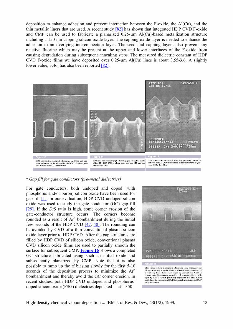
As already noted, HDP CVD is a simultaneous deposition/etching process. The deposition/sputter-rate ratio (D/S) is an important parameter with respect to the gap-filling capability of the processes.For 0.25/0.18-µm structures with 2-2.5 aspect ratios, the best gap filling is achieved with a D/S ratioin the 3.0-3.5 range. Figures 13 and 14 show typical 0.25- and sub-0.25-µm Al(Cu) interconnectionvoid-free gap-fill structures. It can be seen that the gap-fill process is highly directional, with a"bottom-up" fill profile, as has also been observed by others [21, 37]. In a dense metal pattern,partial local planarization can be obtained over the structure using a high D/S level (Figure 13).However, truly global planarization of sub-half-micron structures requires an additional CMP step.In IBM, high-density-plasma CVD interlevel dielectric (ILD) oxide layers have been introducedinto 0.35-µm logic and SRAM manufacturing [79] with excellent gap-fill capabilities. Forintegrated 0.25- and sub-0.25-µm interconnections, HDP CVD processing showed superior gap-fillcapabilities compared to sub-atmospheric TEOS/O3 processing [33, 80] and required fewerprocessing steps than a spin-on-polymer etch-back process [81]. No significant increase in gatebreakdown failure rate was observed for 0.25- and 0.35-µm devices having a 50-65-Å-thick gateoxide and coated with an HDP CVD oxide ILD [29, 33, 81]. For F-oxide films, high- aspect-ratio(>2.5:1) 0.20-µm void-free gap-fill Al(Cu)-based interconnection structures can easily be achieved(Figure 15). Thin (100-300-Å-thick) plasma-deposited oxide films are used prior to F-oxide film
High-density chemical vapour deposition ... IBM J. of Res. & Dev., 43(1/2), 1999. 13
deposition to enhance adhesion and prevent interaction between the F-oxide, the Al(Cu), and thethin metallic liners that are used. A recent study [82] has shown that integrated HDP CVD F-oxideand CMP can be used to fabricate a planarized 0.25-µm Al(Cu)-based metallization structureincluding a 150-nm capping silicon oxide layer. The capping oxide layer is needed to enhance theadhesion to an overlying interconnection layer. The seed and capping layers also prevent anyreactive fluorine which may be present at the upper and lower interfaces of the F-oxide fromcausing degradation during subsequent annealing steps. The measured dielectric constant of HDPCVD F-oxide films we have deposited over 0.25-µm Al(Cu) lines is about 3.55-3.6. A slightlylower value, 3.46, has also been reported [82].
• Gap fill for gate conductors (pre-metal dielectrics)
For gate conductors, both undoped and doped (withphosphorus and/or boron) silicon oxide have been used forgap fill [1]. In our evaluation, HDP CVD undoped siliconoxide was used to study the gate-conductor (GC) gap fill[29]. If the D/S ratio is high, some corner erosion of thegate-conductor structure occurs: The corners becomerounded as a result of Ar+ bombardment during the initialfew seconds of the HDP CVD [47, 48]. The rounding canbe avoided by CVD of a thin conventional plasma siliconoxide layer prior to HDP CVD. After the gap structures arefilled by HDP CVD of silicon oxide, conventional plasmaCVD silicon oxide films are used to partially smooth thesurface for subsequent CMP. Figure 16 shows a completedGC structure fabricated using such an initial oxide andsubsequently planarized by CMP. Note that it is alsopossible to ramp up the rf biasing slowly for the first 5-10seconds of the deposition process to minimize the Ar+
bombardment and thereby avoid the GC corner erosion. Inrecent studies, both HDP CVD undoped and phosphorus-doped silicon oxide (PSG) dielectrics deposited at 350-

High-density chemical vapour deposition ... IBM J. of Res. & Dev., 43(1/2), 1999. 14
400°C have also been used as gap-fill materials for ULSI devices [76, 77]. In one study, acomposite HDP CVD silicon undoped oxide gap fill and plasma-CVD-doped silicate glass filmwere deposited and successfully integrated into a 0.25-µm CMOS device process to achieve betterpre-metal GC gap fill while causing no degradation impact on the CMOS device performance [76].For HDP CVD PSG films with phosphorus concentrations in the 3.5-6.5 wt.% range, subsequentannealing at higher temperature (700°C) was required for film stabilization. An extensive gap-filland film characterization study of HDP CVD PSG on CMOS devices indicated improved gap fill atlower processing temperatures compared to CMOS devices processed with higher-temperature(850°) CVD BPSG films [77]. Because of the excellent gap-filling capability of the HDP CVD PSGprocess and its low thermal budget, it offers another promising alternative to current TEOS/O3
BPSG or conventional CVD BPSG as a pre-metal dielectric CVD process for sub-0.25-µm circuits,provided metal contamination can be kept to a minimal level.
• Gap fill for shallow-trench isolation
Until recently, the low-pressure CVD TEOS/O2 process had been used to deposit high-qualitysilicon oxide dielectrics for shallow-trench isolation (STI) in ULSI devices [83]. As the aspect ratiofor the STI structures becomes larger (>1.2:1), the standard LPCVD process no longer meets gap-fill requirements. With an advanced TEOS/O3 CVD oxide gap-fill process, higher- aspect-ratio sub-half-micron structures with a gradual sloped profile can be filled without voids [1]. For STI, theconsistency of void-free gap fill has a very significant effect on the subsequent STI integrationprocess steps and on final device yield and performance. To improve ULSI CMOS deviceperformance and packing density, vertical STI slope structures with a higher aspect ratio (2:1) mustbe filled with void-free high-quality oxide dielectric. In this case, the advanced TEOS/O3 CVDprocess may not satisfy that requirement, causing the STI gap-fill structures to form a void in a fillcenter [45]. This void at the center of the filled dielectric becomes larger as the aspect ratioincreases, and it is especially large in structures with reentrant slopes. For a sub-half- micronvertical-profile high-aspect-ratio structure, HDP CVD of undoped oxide provides an excellentalternative to conventional LPCVD TEOS/O2 and TEOS/O3 processes [78]. Figure 17 shows a0.25-µm STI structure, having a 1.8:1 aspect ratio, filled with HDP CVD silicon oxide. It can beseen that the gap fill is excellent, and the film density is quite good. No voids were observed in thefilled center, even after buffered HF highlight etching. STI structures with aspect ratios up to 3:1have also been filled with no voids, using the HDP CVD process [45, 79]. As in the case of GC gapfill, corner erosion can be reduced with a PECVD oxide layer before HDP CVD deposition or byramping up the rf bias (i.e., increasing the sputtering component after deposition of a thin seedlayer) during the initial HDP CVD process. For STI, HDP CVD gap fill easily meets therequirement. The major issues are process integration and metal contamination.
From a process-integration viewpoint, it is more difficult to integrate the HDP CVD gap-fill processinto STI process-integration schemes than the conventional LPCVD oxide deposition process. Inthe LPCVD oxide deposition process, the deposited film thickness and profile are more predictableand, in most cases, independent of pattern structure and density. In the TEOS/O3 process, thispattern-density dependency becomes more complex [1]; for HDP CVD, this is one of theintegration issues that will require significant effort to resolve. The pattern-density dependency inHDP CVD arises from the concurrent deposition/etching properties of the process; it has also beenobserved for HDP CVD gap fill of ILD structures [84]. The material deposited in the area on ornear the corner and step structure is sputter-etched (by Ar+) more readily than in a planar area.Furthermore, the deposition parameters, aspect ratios, and dimensions of the gap-fill structures alsoaffect the amount of material deposited on surfaces, indicating that the D/S value of the processdoes not remain constant during deposition. The value changes dynamically and locally withdeposited surface topography and substrate parameters during deposition.

High-density chemical vapour deposition ... IBM J. of Res. & Dev., 43(1/2), 1999. 15
HDP CVD films deposited over complexsubmicron topography structures with moreholes and trenches to fill are considerably thinnerthan those deposited over structures containingfewer topological features. This variation can bepartially reduced by two-step deposition: fillingthe structure partially by HDP CVD of an oxideto reduce the gap-fill aspect ratio, followed bydeposition, either by PECVD of an oxide orLPCVD of an oxide. Since the planarizationrequirement and control of the ULSI STI processare expected to be much more stringent thanthose of GC and ILD structures, integration willbecome more difficult and will require the use ofprocess-integration sequences similar to thosementioned in recent publications [45, 78].Plasma damage, especially at device edges, canbe eliminated by the use of a suitable process-integration scheme [45]. Figure 18 showsmultilevel 0.25-µm ULSI CMOS structures inwhich the STI and GC were filled with an HDPCVD oxide and subsequently planarized byCMP. It should be noted that the thicknessdifferences over the STI structures may causesubsequent process integration problems andmay result in overpolishing of STI oxide in someareas, as shown in the lower portion of thefigure. STI structures having 0.17-µmdimensions and up to a 3.5:1 aspect ratio havealso been deposited with HDP CVD oxide filmswith no voids [45]. It can thus be seen that goodgap fill and planarization can be achieved withHDP CVD processing for sub-half-micron STIwith suitable process integration.
If there is one critical problem that will preventthe use of HDP CVD silicon oxide films in STIgap-fill applications, it is metal contamination.For ULSI STI applications, only a small level ofmetal contamination (>1 x 1015 cm-3) indeposited films will cause unwanted diffusion insubsequent high- temperature (850-1000°C)annealing steps, and deleteriously affect deviceperformance. For mobile ions such as Na+ and
Li+, the contamination threshold may have to be even lower. As mentioned before, the high-densityplasma Ar+ sputtering required for high-aspect-ratio gap fill will also sputter off the metals (Al, Fe,Ni) from the alumina domes that are currently used in most commercial ICP HDP CVD reactorsand cause subsequent metal contamination in deposited films. The high-rate, high-energy fluorine-based plasma-cleaning step for the HDP CVD reaction after deposition may also cause (minusculeamounts of) metal contamination in the reactor and subsequently in the deposited STI oxide films.If HDP CVD silicon oxide is used for ULSI STI fabrication in manufacturing, various metal-

High-density chemical vapour deposition ... IBM J. of Res. & Dev., 43(1/2), 1999. 16
contamination monitors and process controls will have to be implemented to ensure that thecontamination is consistently below acceptable levels. A recent study [32] has shown that themobile ion level in advanced HDP CVD systems can be consistently maintained at relatively lowlevels. However, even at these levels the contamination is still higher than those of LPCVDTEOS/O2 and may be unacceptable for sub-0.25-µm STI oxide gap-fill dielectric applications.Whether this level of metal contamination can be reduced further and/or maintained at sufficientlylow levels during deposition in an HDP CVD system and deposited films will probably be one ofthe factors which determine whether the HDP CVD oxide gap-fill process will be used for futureSTI applications.
Summary
In this paper, we have presented and reviewed recent developments in the HDP CVD of siliconoxide, fluorine-doped silicon oxide, and other carbon and fluorocarbon low-dielectric-constantfilms of current interest in integrated- circuit fabrication. Dielectric films deposited by HDP CVDprocessing not only have better gap-fill properties but also have improved physical, chemical, andelectrical properties compared to those produced by the conventional plasma CVD process. ForIMD applications, the HDP CVD of silicon oxide has performance and cost advantages, and hasbeen implemented for forming IMD dielectrics in IBM sub-half-micron ULSI CMOSmanufacturing. Significant progress has also been made in the HDP CVD of fluorinated siliconoxide. With regard to HDP CVD silicon oxide and PGS film applications to shallow-trenchisolation (STI) and gate-conductor (GC) gap fill, issues pertaining to metal contamination andprocess integration continue to be of concern. HDP CVD carbon and fluorocarbon films may beuseful in conjunction with low-k objectives, but it may be less costly to use conventional plasmaCVD for depositing such films. Nevertheless, the results covered in this paper suggest that if themetal-contamination and process-integration concerns can be effectively addressed, the HDP CVDprocess may play an important role in the future fabrication of integrated circuits.
Acknowledgments
Some of the work in this paper was implemented under the alliance among IBM, Siemens, andToshiba to develop 256Mb DRAM. I would like to thank the IBM Advanced SemiconductorTechnology Center for their support. I would also like to express my appreciation to Donna Cote,Jim Ryan, Mike Shapiro, Dave Dobuzinsky, Rosemary Christie, Gregory Fitzgibbon, ChetDziobkowski, G. Freeman, K. Kellerher, Nancy Klymko, Arsam Anstreasyan, and Yi S. Huang ofIBM; Katsuya Okumura, N. Shoda, and Tetsuo Matsuda of Toshiba; Peter Weigand of Siemens;Jake Rzuzeck, Linda Roger, R. Nowak, T. Sahin, and D. Witty of Applied Materials; and TomMontsieur of Novellus for their contributions, assistance, support, and valuable discussions withrespect to some of the experimental work covered in the paper. The assistance of the managementof the IBM Storage Systems Division is highly appreciated.
References1.D. R. Cote, S. V. Nguyen, W. J. Cote, S. L. Pennington, A. K. Stamper, and D. V. Podlesnik, "Low-Temperature
Chemical Vapor Deposition Processes and Dielectrics for Microelectronic Circuit Manufacturing at IBM," IBM J.Res. Develop. 39, 437-464 (1995) and references therein.
2.S. P. Muraka, "Multilevel Interconnection for ULSI and GSI Era," Mater. Sci. & Eng. R19, 87-151 (1997).3.P. Singer, "Low-k Dielectrics: The Search Continues," Semicond. Int. 19, 88-98 (1996); "Copper Opportunities and
Challenges Review at SRC Workshop," Semicond. Int. 16, 50-55 (1993).4.A. K. Stamper, V. McGahay, and J. P. Hummel, "Intermetal Dielectrics--A Five Year Outlook," Proceedings of the
Third International Dielectrics for ULSI Multilevel Interconnection Conference, 1997, pp. 13-15.5.T. Usami, K. Shimokawa, and M. Yoshimaru, "Low Dielectric Constant Interlayer Using Fluorine-Doped Silicon
Oxide," Jpn. J. Appl. Phys. 33, 408-412 (1994).6.M. J. Shapiro, S. V. Nguyen, T. Matsuda, and D. Dobuzinsky, "CVD of Fluorosilicate Glass for ULSI Applications,"
Thin Solid Films 270, 503-507 (1995).7.S. V. Nguyen, P. Weigand, J. Rzuzeck, M. J. Shapiro, and C. Dziobkowski, "High Density Plasma Deposition and
Characterization of F-Oxide Films," Proceedings of the 13th International Symposium in Plasma Chemistry, Vol. 3,

High-density chemical vapour deposition ... IBM J. of Res. & Dev., 43(1/2), 1999. 17
C. K. Wu, Ed., Peking University Press, Beijing, China, 1998, pp. 1153-1158.8.G. Sugahara, N. Aoi, M. Kubo, K. Arai, and K. Sawada, "Low Dielectric Constant Carbon Containing SiO2 Films
Deposited by PECVD Technique Using a Novel CVD Precursor," Proceedings of the Third International Dielectricsfor ULSI Multilevel Interconnection Conference, 1997, pp. 19-25.
9.S. McClatchie, K. Beekmann, A. Kiermasz, and C. Dobson, "Low Dielectric Constant Flow Fill Technology for IMDApplications," Proceedings of the Third International Dielectrics for ULSI Multilevel Interconnection Conference,1997, pp. 39-40.
10.T. N. Nguyen, G. S. Oehrlein, and Z. A. Wienberg, "Plasma Deposition of Fluorocarbon," U.S. Patent 5,302,420,April 12, 1994.
11.A. Grill and V. Patel, "Wear Resistant Fluorinated Diamond Like Carbon," Diamond Films & Technol. 6, 13-21(1996); "Diamond Like Carbon Materials as Low-k Dielectrics for Multilevel Interconnect in ULSI," Mater. Res.Soc. Symp. Proc. 443, 155-162 (1997).
12.K. Endo and T. Tatsumi, "Fluorinated Amorphous Carbon Thin Films Grown by Plasma Enhanced CVD for LowDielectric Constant Interlayer Dielectrics," J. Appl. Phys. 78, 1370-1372 (1995).
13.S. Robles, L. Vasquez, M. Eizenberg, and F. Moghadam, "Characterization of High Density Plasma Deposited a-Carbon and a-Fluorinated Carbon Films for Ultra Low Dielectric Applications," Proceedings of the ThirdInternational Dielectrics for ULSI Multilevel Interconnection Conference, 1997, pp. 26-33.
14.S. J. Limb, K. K. Gleason, D. J. Edel, and E. F. Gleason, "Flexible Fluorocarbon Wired Coating by Pulse PlasmaEnhanced Chemical Vapor Deposition," J. Vac. Sci. Technol. A 15, 1814-1818 (1997).
15.H. Kudo, S. Takeishi, R. Shinohara, and M. Yamada, "Characteristics of Plasma C-F Films for Very Low-kDielectrics," Proceedings of the Third International Dielectrics for ULSI Multilevel Interconnection Conference,1997, pp. 85-92.
16.K. Endo, T. Tatsumi, Y. Matsubara, M. Iguchi, and T. Horiuchi, "Improvement of the Thermal Stability of Low-kFluorinated Amorphous Carbon Layer by Controlling F/C Ratio," Proceedings of the Fourteenth International VLSIMultilevel Interconnection Conference, 1997, pp. 547-552, and references therein.
17.M. A. Lieberman and R. A. Gottcho, "Design of High Density Plasma Source for Material Processing," pp. 1-119;and O. A. Popov, "Electron Cyclotron Resonance Plasma Sources and Their Use in Plasma-Assisted ChemicalVapor Deposition of Thin Films," pp. 121-233, in Physics of Thin Films: Plasma Source for Thin Film Depositionand Etching, Vol. 18, M. H. Francombe and J. L. Vossen, Eds., Academic Press, Inc., New York, 1994.
18.O. A. Popov, High Density Plasma Source Design, Physics and Performance, Noyes Publications, Park Ridge, NJ,1995.
19.A. Bose, M. M. Graver, and R. A. Spencer, "Advanced Intermetal Dielectric Deposition--A Comparative AnalysisBetween ECR-CVD and O3/TEOS," Proceedings of the 10th International VLSI Multilevel InterconnectionConference, 1993, pp. 89-95.
20.S. V. Nguyen and K. Albaugh, "The Characterization of Electron Cyclotron Resonance Plasma Deposited SiliconNitride and Silicon Oxide Films," J. Electrochem. Soc. 136, 2835-2840 (1989) and references therein.
21.K. Kato, K. Kobayashi, and A. Takamatsu, "Gap Filling Mechanism in Si Film Deposition by Using Bias ECR CVDSystem," Proceedings of the Third International Dielectrics for ULSI Multilevel Interconnection Conference, 1997,pp. 67-70.
22.N. Jiang, B. Agius, M. C. Hugon, J. Olivier, and M. Puech, "Radio-Frequency Bias Effect on SiO2 Films Depositedby Distributed ECR Plasma Enhanced Chemical Vapor Deposition," J. Appl. Phys. 76, 1847-1855 (1997).
23.S. Bothara, C. T. Gabriel, S. Lassig, and D. Pirkle, "Control of Plasma Damage to Gate Oxide During High DensityPlasma Chemical Vapor Deposition," J. Electrochem. Soc. 142, L208-L211 (1995).
24.D. E. Kotecki and J. D. Chapple-Sokol, "Hydrogen Incorporation in Silicon Nitride Films Deposited by RemoteElectron Cyclotron Resonance Plasma," J. Appl. Phys. 77, 1284-1293 (1995).
25.C. Ye, Z. Ning, M. Shen, H. Wang, and Z. Gan, "Dielectric Properties of Silicon Nitride Films Deposited byMicrowave Electron Cyclotron Resonance Plasma Chemical Vapor Deposition at Low Temperature," Appl. Phys.Lett. 71, 336-337 (1997).
26.C. Charles, R. W. Boswell, and H. Kuwahara, "SiO2 Deposition from Oxygen/Silane Pulse Helicon DiffusionPlasma," Appl. Phys. Lett. 67, 40-42 (1995).
27.N. Hayasaka, Y. Nishiyama, H. Miyajima, K. Tomioka, R. Nakata, and H. Okano, "High Quality Low DielectricConstant SiO2 CVD Using High Density Plasma," Proceedings of the Dry Process Symposium, 1993, pp. 163-168.
28.C. Charles, G. Giroult-Matlakkowski, R. B. Boswell, A. Goullett, G. Turban, and C. Cardinaud, "Characterization ofSiO2 Film Deposited at Low Pressure and Temperature in a Helicon Diffusion Reactor," J. Vac. Sci. Technol. A 11,2954-2963 (1993).
29.S. V. Nguyen, G. Freeman, D. Dobuzinsky, K. Kellerher, R. Nowak, T. Sahin, and D. Witty, "Characterization ofHigh Density Plasma Deposited Silicon Oxide Dielectric for 0.25 µm ULSI," Proceedings of the 12th InternationalVLSI Multilevel Interconnection Conference, 1995, pp. 69-75.
30.J. Kim, D. Kim, J. Hong, J. Kim, M. Jung, K. Koo, H. Lim, Y. Lim, M. Han, J. S. Choi, and M. Y. Lee, "Applicationof High Density Plasma to 1 Gbit DRAM for ILD," Proceedings of the Fourteenth International VLSI MultilevelInterconnection Conference, 1997, pp. 623-625.
31.L. Murugesh, M. Orezyk, J. Hamila, M. Ozkan, P. Narwanka, J. Qiao, S. Li, Y. Wang, T. Shahin, and F.Moghaddam, "Process Window Characterization of ULTIMA HDP-CVD Low Dielectric FSG," Proceedings of theThird International Dielectrics for ULSI Multilevel Interconnection Conference, 1997, pp. 387-394.
32.Y. Wang, I. Valle, S. Ritterbush, J. Qiao, C. Chan, S. Li, P. Narwankar, J. Hamila, A. Collins, T. Shahin, C. Leung,and F. Moghaddam, "Process Window Characterization of ULTIMA HDP-CVD USG Films," Proceedings of theThird International Dielectrics for ULSI Multilevel Interconnection Conference, 1997, pp. 405-408.
High-density chemical vapour deposition ... IBM J. of Res. & Dev., 43(1/2), 1999. 18
33.P. Weigand, H. Palm, E. W. Kiewra, and S. V. Nguyen, "Integration of Dielectrics for 0.25 µm Metallization Levels:HDP-CVD Versus SA-CVD," Proceedings of the Fourteenth International VLSI Multilevel InterconnectionConference, 1997, pp. 565-570 and references therein.
34.V. G. M. Van den Hoek and T. W. Mountsier, "A New High Density Plasma Source for Void Free Dielectric GapFill," presented at the Semicon Japan Technical Symposium, Tokyo, 1994.
35.W. G. M. Van den Hoek, J. Bondur, B. Van Schravendijik, C. Roberts, and C. Cunningham, Proceedings of theSecond International Dielectrics for ULSI Multilevel Interconnection Conference, 1996, pp. 103-107.
36.S. Matsuo, "Microwave Electron Cyclotron Resonance Plasma Chemical Vapor Deposition," Handbook of Thin-Film Deposition Processes and Techniques, K. K. Schuegraf, Ed., Noyes Publications, Park Ridge, NJ, 1988, pp.147-169.
37.S. Lassig and J. Tucker, "Electron Cyclotron Resonance CVD Lam Epic System," Lam Research Technical LibraryTL 019, March 1993, and Lam Research Thin Film Interface 4, No. 3, 3 (August 1993).
38.B. Fowler and E. O'Brien, "Relationship Between Material Properties of Silicon Dioxide Deposited by ECR CVDand Their Use as Indicators of the Dielectric Constant," J. Vac. Sci. Technol. B 12, 441-448 (1994) and referencestherein.
39.S. V. Nguyen, D. Dobuzinsky, D. Harmon, R. Gleason, and S. Fridmann, "Reaction Mechanism of Plasma andThermal-Assisted Chemical Vapor Deposition of Tetraethylorthosilicate Oxide Films," J. Electrochem. Soc. 137,2209-2215 (1990) and references therein.
40.John Baliga, "Vacuum Pump Design Adjusted to Harsher Conditions," Semicond. Int. 20, No. 12, 86-90 (1997).41.J. Field, "Electrostatic Wafer Clamping for Next-Generation Manufacturing," Solid State Technol. 37, No. 9, 91-98
(1994).42.K. A. Olson, D. Kotecki, A. J. Ricci, S. E. Lassig, and A. Husain, "Characterization, Modeling, and Design of an
Electrostatic Chuck with Improved Wafer Temperature Uniformity," Rev. Sci. Instrum. 66, 1108-1114 (1995).43.P. Singer, "Electrostatic Chuck in Wafer Processing," Semicond. Int. 18, No. 4, 57-64 (1995) and references therein.44.M. Nakasuji, "Low Voltage and High Speed Operating Electrostatic Wafer Chuck Using Sputtered Tantalum
Oxide," J. Vac. Sci. Technol. A 12, No. 5, 2834-2838 (1994).45.S. Nag and A. Chatterjee, "Shallow Trench Isolation for Sub-0.25µm IC Technologies," Solid State Technol. 40, No.
9, 129-136 (1997).46.S. Bothra, C. T. Gabriel, S. Lasig, and D. Pirkle, "Control of Plasma Damage to Gate Oxide During High Density
Plasma Chemical Vapor Deposition," J. Electrochem. Soc. 142, No. 11, L208-L211 (1995).47.S. V. Nguyen and P. Pan, "The Initial Transient Phenomena in Plasma Enhanced Chemical Vapor Deposition
Process," Appl. Phys. Lett. 45, 134-136 (1984).48.Y. Nakayama, T. Ohtsuchi, and T. Kawamura, "A Study of Initial Transient Phenomena in the Chemical Vapor
Deposition Process Using Silane Plasma," J. Appl. Phys. 62, No. 3, 1022-1028 (1997).49.S. V. Nguyen, W. A. Lansford, and A. L. Rieger, "Variation of Hydrogen Bonding, Depth Profiles and Spin Density
of Plasma Deposited Silicon Nitride and Oxynitride with Deposition Mechanism," J. Electrochem. Soc. 133, No. 5,970-974 (1986).
50.Tetsuo Matsuda, Mike Shapiro, and S. V. Nguyen, "Dual Frequency Plasma CVD Fluorosilicate Glass for 0.25 µmILD," Proceedings of the First Dielectric for ULSI International Conference (DUMIC), 1995, pp. 22-28.
51.D. Cote, A. Antreasyan, D. Podlesnik, and A. LeBlanc, "PECVD Process-Induced Gate Oxide Degradation in64Mbit DRAM," Abstract H2.04, Abstracts of the 1995 International Conference on Metallurgical Coatings andThin Films, American Vacuum Society, p. 257.
52.G. C. Schwartz, Y. S. Huang, and W. J. Patrick, "The Effective Dielectric Constant of Silicon Dioxides Deposited inthe Spaces Between Adjacent Conductors," J. Electrochem. Soc. 139, No. 12, L118-L122 (1992).
53.S. V. Nguyen, D. Dobuzinsky, J. Ryan, M. Shapiro, and T. Matsuda, "PECVD Method of Depositing FluorineDoped Oxide Using a Fluorine Precursor Containing a Glass-Forming Element," U.S. Patent 5,563,105, 1996.
54.Son V. Nguyen, M. J. Shapiro, T. Matsuda, D. Dobuzinsky, and C. T. Dziobkowski, "Plasma Deposition Chemistryof Fluorinated Silicon Oxide Films," Proceedings of the 12th International Symposium in Plasma Chemistry, Vol. 4,J. V. Heberlein, D. W. Ernie, and J. T. Robert, Eds., IUPAC, Minneapolis, August 21-25, 1995, pp. 1975-1980.
55.T. Fukuda, E. Sasaki, T. Hosokawa, K. Kato, and N. Koboyashi, "Highly Reliable SiOF Film Formation UsingHigh Density Plasma Containing Hydrogen," Proceedings of the Third International Dielectrics for ULSI MultilevelInterconnection Conference, 1997, pp. 41-48.
56.H. Yoshitaka, T. Tamura, Y. Inoue, M. Satoh, and J. Sakai, "Biased Helicon-Plasma CVD of Low-k Dielectric for0.2 Micron ULSI Metallization," Proceedings of the Third International Dielectrics for ULSI MultilevelInterconnection Conference, 1997, pp. 70-82.
57.M. Hayashi, K. Ohhira, H. Watatani, K. Suzuki, K. Koyama, and H. Yagi, "High Density Plasma CVD Fluoro-Silicate Glass Gap-Filling for Sub-Half Micron CMOS Devices," Proceedings of the Third International Dielectricsfor ULSI Multilevel Interconnection Conference, 1997, pp. 205-212.
58.W. Tseng, Y. Hsieh, C. Lin, M. Tsai, and M. Feng, "Chemical Mechanical Polishing and Material Characterizationof Plasma-Enhanced Chemical Vapor Deposited Fluorinated Oxide Thin Films," J. Electrochem. Soc. 144, No. 3,1100-1106 (1997).
59.K. M. Chang, S. W. Wang, T. H. Yeh, C. H. Li, and J. J. Luo, "Leakage Performance and Breakdown Mechanism ofSilicon-Rich Oxide and Fluorinated Oxide Prepared by Electron Cyclotron Resonance Chemical Vapor Deposition,"J. Electrochem. Soc. 144, No. 5, 1754-1759 (1997).
60.R. Swope, W. S. Yoo, J. Hsieh, S. Shuchmann, F. Nagy, H. Nijenhuis, and D. Moro, "Improvement of AdhesionProperties of Fluorinated Glass Films by Nitrous Oxide Plasma Treatment," J. Electrochem. Soc. 144, No. 7, 2559-2564 (1997).

High-density chemical vapour deposition ... IBM J. of Res. & Dev., 43(1/2), 1999. 19
61.Son V. Nguyen, "Plasma Enhanced Chemical Vapor Deposition," Handbook of Thin Film Deposition Processes andTechniques, K. Schuegraf, Ed., Noyes Publications, Park Ridge, NJ, 1988, pp. 112-141.
62.S. W. Lim, Y. Shimogaki, Y. Nakano, K. Tada, and H. Komiyama, "Reduction Mechanism in the DielectricConstant of Fluorine-Doped Silicon Oxide Film," J. Electrochem. Soc. 144, No. 7, 2531-2537 (1997).
63.G. Lucovsky and H. Yang, "Fluorine Atom Induced Decreases to the Contribution of Infrared Vibrations to theStatic Dielectric Constant of Si-O-F Alloy Films," J. Vac. Sci. Technol. A 15, No. 3, 836-843 (1997).
64.David Lammers, "Lam Research Chief Maps Broader Role in CVD," Electronic Engineering Times, October 20,1997, p. 24; "Intel Claims Its 0.18µm Al Process Beats Copper," Electronic Engineering Times, December 14, 1998,p. 22.
65.S. Takeishi, H. Kudo, R. Shinohara, M. Hoshino, S. Fukuyama, J. Yamaguchi, and M. Yamada, "Plasma-EnhancedChemical Vapor Deposition of Fluorocarbon Films with High Thermal Resistance and Low Dielectric Constants," J.Electrochem. Soc. 144, No. 5, 1797-1802 (1997).
66.S. H. Kim, Y. S. Park, S. K. Jung, D. H. Kang, and J. W. Lee, "Effect of Substrate State on the Formation ofDiamond Film in a Low Temperature Microwave-Plasma-Enhanced Chemical Vapor Deposition System," J. Vac.Sci. Technol. A 13, No. 3, 1619-1623 (1995).
67.L. H. Chou and W. T. Hsieh, "Effect of Argon Ion Bombardment on the Microstructures and ElectricalConductivities of Hydrogenated Amorphous Carbon Films Prepared by Plasma-Enhanced Chemical VaporDeposition," J. Appl. Phys. 75, No. 4, 2257-2263 (1997).
68.G. S. Oehrlein, Y. Zhang, D. Vender, and M. Haverlag, "Fluorocarbon High Density Plasma. I. Fluorocarbon FilmDeposition and Etching Using CF4 and CHF3," J. Vac. Sci. Technol. A 12, No. 2, 323-332 (1994).
69.P. S. Andry, P. W. Pastel, and W. J. Varhue, "Comparison of Diamond-Like Carbon Film Deposition by ElectronCyclotron Resonance with Benzene and Methane," J. Mater. Res. 11, No. 1, 221-228 (1996).
70.P. K. Bachman, "Microwave Plasma Chemical Vapor Deposition of Diamond," Handbook of Industrial Diamondand Diamond Films, Ch. 11, M. A. Prelas, G. Povovici, and L. K. Bigelow, Eds., Marcel Dekker Inc., New York,1997, pp. 821-850.
71.C. B. Labelle, S. J. Limb, K. K. Gleason, and J. A. Burns, "Characterization of Pulse-Plasma Enhanced ChemicalVapor Deposited Fluorocarbon Thin Film," Proceedings of the Third International Dielectrics for ULSI MultilevelInterconnection Conference, 1997, pp. 98-105.
72.E. Korczynski, "Low-k Dielectric Integration Cost Modelling," Solid State Technol. 40, No. 10, 123-128 (1997).73.J. G. Ryan, R. M. Geffken, N. R. Poulin, and J. R. Paraszczak, "The Evolution of Interconnection Technology at
IBM," IBM J. Res. Develop. 39, No. 4, 371-381 (1995) and references therein.74.S. J. Limb, C. B. Labelle, K. K. Gleason, D. J. Edell, and E. F. Gleason, "Growth of Fluorocarbon Polymer Thin
Film with High CF2 Fraction and Low Dangling Bond Concentrations by Thermal Chemical Vapor Deposition,"Appl. Phys. Lett. 68, No. 20, 2810-2812 (1996).
75.P. Singer, "Future of Dielectric CVD: High Density Plasma?" Semicond. Int. 20, No. 8, 126-134 (1997).76.C. Chen, J. Y. Wu, W. Lur, and S. W. Sun, "A Pre-Metal Dielectric Process for 0.25 Micron CMOS and Beyond,"
Proceedings of the Fourteenth International VLSI Multilevel Interconnection Conference, 1997, p. 657. 77.Y. Gobil, P. Fugier, Y. Morand, H. M'Saad, and T. Veyron, "High Density Plasma CVD Phosphorous Silicon Glass
for Pre-Metal Application in Sub-0.25 Micron CMOS Technology," Proceedings of the Second InternationalDielectrics for ULSI Multilevel Interconnection Conference, 1996, pp. 108-115.
78.V. C. Patriek, H. W. Ery, V. S. Baer, and V. d. H. Wilbert, "HDPCVD Films Enabling Shallow Trench Isolation,"Semicond. Int. 20, No. 8, 179-186 (1997).
79.H. K. Lee, A. K. Stamper, D. Bouldin, S. Luce, T. McDevitt, W. Murphy, and S. Greco, "A Manufacturing Five-Level-Metal Fully Planarized 0.35-Micron Generation Back-End-Of-The-Line (BEOL) for Logic and SRAM,"Proceedings of the Fourteenth International VLSI Multilevel Interconnection Conference, 1997, pp. 25-30.
80.C. C. Liu, W. Lur, and S. W. Sun, "Integrated HDP Technology for Sub-0.25 Micron Gap Fill," Proceedings of theFourteenth International VLSI Multilevel Interconnection Conference, 1997, pp. 618-619.
81.J. Zheng, C. Chia, Y. Xu, S. Y. M. Chooi, L. Chan, and Y. S. Lin, "A Comparison of HDP Oxide and Spin-On-Polymer for Intermetal Dielectrics Application in Sub-Half Micron Devices," Proceedings of the Third InternationalDielectrics for ULSI Multilevel Interconnection Conference, 1997, pp. 283-286.
82.Y. Shimooka, T. Matsuno, A. Ui, H. Mijayima, N. Kaji, H. Nojo, Y. Tateyama, and H. Shibata, "Fully PlanarizedHigh Density Plasma CVD Fluorine Doped ILD," Proceedings of the Fourteenth International VLSI MultilevelInterconnection Conference, 1997, pp. 119-124.
83.K. Bluenenstock, J. Thiesen, P. Pan, J. Dulack, A. Ticknor, and T. Sandwick, "Shallow Trench Isolation for Ultra-Large-Scale Integrated Devices," J. Vac. Sci. Technol. B 12, No. 1, 54-58 (1994).
84.P. Wiegand, N. Shoda, T. Matsuda, S. Nguyen, J. Rzuczek, M. J. Shapiro, T. Jones, and R. Ploessi, "HDP CVDSilicon Oxide Deposition: The Effect of Sputtering on Film Properties," Proceedings of the 13th International VLSIMultilevel Interconnect Conference (VMIC), 1996, pp. 75-80.
Received January 12, 1998; accepted for publication June 8, 1998
*See also the paper by A. Grill in this issue.