voltage mode electronically tunable full-wave rectifier papers/midem_46(2016)4p229.pdf · 230 in...
TRANSCRIPT

229
Original scientific paper
MIDEM Society
Voltage Mode Electronically Tunable Full-wave RectifierPredrag B. Petrović
University of Kragujevac, Faculty of Technical Sciences Čačak, Čačak, Serbia
Abstract: The paper presents a new realization of bipolar full-wave rectifier of input sinusoidal signals, employing one MO-CCCII (multiple output current controlled current conveyor), a zero-crossing detector (ZCD), and one resistor connected to a fixed potential. The circuit provides the operating frequency up to 10 MHz with increased linearity and precision in processing of low-level input voltage signal, with a very low harmonic distortion. The errors related to the signal processing and errors bound were investigated and provided in the paper. The PSpice simulations are depicted and agree well with the theoretical anticipation. The maximum power consumption of the converter is approximately 2.83 mW, at ±1.2 V supply voltages.
Keywords: bipolar transistor circuits; circuit analysis; circuit simulation; error analysis; rectifiers
Napetostni elektronsko nastavljiv polnovalni usmernik Izvleček: Članek predstavlja novo realizacijo bipolarnega polnovalnega usmernika vhodnih sinusnih signalov z uporabo ene MO-CCCII (večizhodni tokovno krmiljen tokovni ojačevalnik), detektorja ničelnega prehoda (ZCD) in upora vezanih na fiksen potencial. Delovna frekvenca vezja je do 10 MHz z naraščajočo linearnostjo in natančnostjo v procesiranju nizko-nivojhih vhodnih napetostnih signalov z nizkim harmoničnim popačenjem. V članku so raziskane in predstavljene napake pri procesiranju signalov. Teoretična predvidevanja so potrjena s počjo PSPice simulacij. Največja poraba energije ojačevalnika je 2.83 mW pri napajalni napetosti ±1.2 V.
Ključne besede: vezja bipolarnega tranzistorja; analiza vezij; simulacije vezij; analiza napak; usmernik
* Corresponding Author’s e-mail: [email protected]
Journal of Microelectronics, Electronic Components and MaterialsVol. 46, No. 4(2016), 229 – 237
1 Introduction
Rectification is the essential and demanding aspect of signal processing in instrumentation, measurement and control. Rectifiers are widely applied in signal pro-cessing, signal–polarity detectors, amplitude modulat-ed signal detectors, AC voltmeters and ampermeters, watt meters, RF demodulators, function fitting error measurements, RMS to DC conversions, sample and hold circuits, peak value detectors, clipper circuits [1-3], etc.. Owing to the threshold voltage of diodes, con-ventional diode rectifiers are limited and are only used in specific applications, such as DC voltage supplies. However, simple diode rectifiers cannot be used for ap-plications requiring accuracy in the threshold voltage range. This can be overcome by using high precision integrated circuit rectifiers.
Although the use of current-mode (CM) active devices is restricted to current processing, it offers certain ad-
vantages such as higher usable gain, more reduced voltage excursion at sensitive nodes, greater linearity, lower power consumption, wider bandwidth, better accuracy and larger dynamic range compared to that of their voltage-mode counterparts. The CCII is a reported active component, especially suitable for the class of analog signal processing. However, the CCII cannot control the parasitic resistance at x (Rx) port, therefore – when it is used in some circuits, it inevitably requires external passive components, especially resistors [2]. This makes it inappropriate for IC implementation, as it occupies a greater chip area, high power dissipation and excludes electronic controllability. On the other hand, the recently introduced second-generation cur-rent controlled conveyor (CCCII) has the advantage of electronic adjustability over the CCII [4]. Also, the use of dual-output current-conveyors is found to be useful in the derivation of current-mode single input circuits.

230
In order to improve performance of OA-based circuits the use of the current conveyor was proposed in [5]. The full-wave rectifier [6], with a single three-output CCCII, two MOS transistors and a resistor with large cross-over distortion, was able to perform rectifica-tion at lower frequencies, e.g. 5 kHz. The papers [7-8] described full-wave rectifier circuits based on usage of two second-generation current conveyors (CCIIs) and four diodes. The rectifier circuits [9-10] offer a wide dy-namic range and show a broadband operation thanks to the use of a CMOS class AB amplifier and current rectifier operation. The rectifier capable of providing output voltages nearly at the level of the input voltage combined with low power consumption is described in [11], which was also achieved through the circuit design proposed here. In [11], CMOS integrated active rectifier concept as an innovative approach for higher efficiencies is used.
A full-wave rectifier proposed in [12] is based on the us-age of two plus-type second-generation current con-veyors (CCII+s) and three MOSFETs. A voltage-mode (VM) rectifier with high-input impedance using dual-X current conveyors (DXCCII) and three MOSFETs, with-out passive components, is described in [13]. In [14], the current-mode (CM) rectifier uses two CCII+s and four diodes. The CM rectifier based on one current con-veyor and one universal voltage conveyor (UVC) and two diodes is introduced in [15]. The circuits proposed in [16] employ at least two current and/or voltage con-veyors as active elements and two diodes, and works in CM. A CM full-wave rectifier circuit with one active ele-ment – current differencing transconductance ampli-fier (CDTA) and four diodes and one resistor is reported in [17]. The circuits proposed in [18-19] are designed based on MOS transistors with fairly simple structure. The rectifier [18] requires a floating input voltage source, while the circuit [19] needs three external bias current sources to be realized separately. The circuits in [20], [21] use CDTA or DXCCII which have more complex internal structures with respect to CCII and DVCC. A CM full-wave rectifier based on a single modified Z-copy current difference transconductance amplifier (MZC-CDTA) and two switches is reported in [22].
This paper presents the principles of operation, and the detailed circuit design of the new bipolar realization of the full-wave rectifier. The features of the proposed cir-cuit are: it employs one MO-CCCII, one zero-crossing detector, and one resistor connected to source voltage, which is suitable for fabrication in a monolithic chip. Unlike the rectifier described in [2-3], which was real-ized using the CMOS technology, the one described in this paper involves a simpler and more accurate con-trol structure. Besides, the proposed circuit does not require a more precise bias voltages realization and
complex transistor pairing, which was typical of the realizations described in [2-3]. The rectifier circuit pro-vides the operating frequency of up to 10 MHz, with increased linearity and precision in processing of low level input voltage signals. The performance of the pro-posed circuit is illustrated by PSpice simulations, show-ing a good agreement with the calculation. The circuits proposed in this paper have been compared to similar circuits reported in literature.
2 Proposed full-wave rectifier circuits
Fig. 1 presents the proposed circuit of the full-wave rec-tifier.
Figure 1: The proposed circuit of the full-wave rectifier
Conceptually, the rectifier presented in Fig. 1 is very similar to the one proposed in [6], the former, however, having more precise and new zero-crossing detection (ZCD) circuits, and without shunting of the high output of MO-CCCII. The proposed ZCD circuits demand con-siderably less resistance in the output stage (50 times) compared to the realization in [6]. This modification en-sures greater linearity rectification within a wider fre-quency range. Additionally, this configuration imposes no limitations in realization of the analog switch, con-trary to the circuit described in [6].
P. B. Petrović; Informacije Midem, Vol. 46, No. 4(2016), 229 – 237
BI
MO-CCCII
x
y z+
z−ini
invSW
LRouti
ZCD
MO-CCCII
yv
xv
yi
xi
+zi
−zi
BI
y
x
z+
z−
Figure 2: Electrical symbol of MO-CCCII
231
Generally, a MO-CCCII is a multiple-terminal active building block, as shown in Fig. 1. The electrical symbol of the MO-CCCII is shown in Fig. 2.
The port relations of the MO-CCCII can be presented by the following equation:
xzxzxxyxy iiiiRivvi −=+=+== −+ ;;;0 (1)
The schematic bipolar realization is shown in Fig. 3 [23]. According to equation (1), the MO-CCCII has a unity voltage gain between terminal y and x and a unity cur-rent gain between terminal x and z. The Rx is an inner resistance of a translinear mixed loop (Q1 to Q4) with grounded resistor equivalent controlled by bias current IB. In this case, the parasitic resistance Rx at the terminal x can be expressed by:
B
Tx I
VR2
= (2)
where VT=26 mV at 27o C is the usual thermal voltage given by kT/q, k=Boltzmann’s constant=1.38×10⁻²³ J/K, T=the absolute temperature (in Kelvin’s), and q= 1.6×10⁻¹⁹ C and IB (Fig. 1) is the bias current of the con-veyor which remains tunable over several decades.
Figure 3: Bipolar realization of MO-CCCII
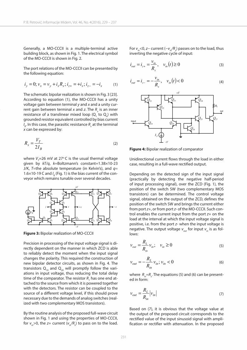
Precision in processing of the input voltage signal is di-rectly dependent on the manner in which ZCD is able to reliably detect the moment when the input signal changes the polarity. This required the construction of new bipolar detector circuits, as shown in Fig. 4. The transistors Q19 and Q20 will promptly follow the vari-ations in input voltage, thus reducing the total delay time of the comparator. The resistor R1 has one end at-tached to the source from which it is powered together with the detectors. The resistor can be coupled to the source of a different voltage level, if this should prove necessary due to the demands of analog switches (real-ized with two complementary MOS transistors).
By the routine analysis of the proposed full-wave circuit shown in Fig. 1 and using the properties of MO-CCCII, for vin>0, the z+ current (vin/Rx) to pass on to the load.
For vin<0, z− current (−vin/Rx) passes on to the load, thus inverting the negative cycle of input:
( ) 0, ≥== + tvRvii inx
inzout (3)
( ) 0, <−== − tvRvii inx
inzout (4)
Figure 4: Bipolar realization of comparator
Unidirectional current flows through the load in either case, resulting in a full-wave rectified output.
Depending on the detected sign of the input signal (practically by detecting the negative half-period of input processing signal), over the ZCD (Fig. 1), the position of the switch SW (two complementary MOS transistors) can be determined. The control voltage signal, obtained on the output of the ZCD, defines the position of the switch SW and brings the current either from port z+, or from port z- of the MO-CCCII. Such con-trol enables the current input from the port z+ on the load at the interval at which the input voltage signal is positive, i.e. from the port z- when the input voltage is negative. The output voltage vout for input vin is as fol-lows:
0; ≥= inin
in
Lout vv
RRv (5)
0; <−= inin
in
Lout vv
RRv (6)
where Rin=Rx. The equations (5) and (6) can be present-ed in form:
in
in
Lout v
RRv = (7)
Based on (7), it is obvious that the voltage value at the output of the proposed circuit corresponds to the rectified value of the input sinusoid signal with ampli-fication or rectifier with attenuation. In the proposed
P. B. Petrović; Informacije Midem, Vol. 46, No. 4(2016), 229 – 237
1Q 2Q
3Q 4Q
5Q6Q
7Q
8Q 9Q 10Q11Q
12Q
14Q13Q
14Q
15Q 17Q
16Q 18Q
BI
xy z+ z−
V+
V−
19Q 20Q25Q
24Q21Q
22Q
26Q
23Q
27Q
PI
V+
out
input
V−
1R
232
circuit, rectification is not performed by diodes, which implies fewer ripples, compared with the known diode rectifier circuits [14-17]. It is also possible to perform low-voltage (below threshold level of the diode) rectifi-cation using the proposed circuit.
3 Non-ideal Effects
The effects of MO-CCCII and comparator non-idealities on the full-wave rectifier performance are to be consid-ered in this section. By considering the non-ideal MO-CCCII characteristics, equation (1) can be rewritten as:
xnzxpzxxyxy iiiiRivvi ββα −=+=+== −+ ;;;0 (8)
where α=1-ev and εv (|εv|<<1) represents the volt-age tracking error from y to x terminal, βp=1-ep and εp (|εp|<<1) denotes the current tracking error from x to z+ terminal, while βn=1-en and εn (|εn|<<1) stands for the current tracking error from x to z- terminal of the MO-CCCII, respectively. Generally, these tracking factors remain constant and frequency independent within low to medium frequency ranges. Typical values of the non-ideal current transfer gains and the transconduct-ance inaccuracy factor α, βp and βn range from 0.9 to 1, with an ideal value of 1. However, at higher frequencies these tracking factors become frequency dependent. Given the non-idealities, currents generated from MO-CCCII can be defined as:
( )in
innpzzout Rviii αββ −=−= +−
' (9)
( ) 0,22' ≥== tvIkTvqI
Vvi inB
inpB
T
inpout
αβαβ (10)
( ) 0,22' <−=−= tvIkTvqI
Vvi inB
innB
T
innout
αβαβ (11)
which results in an absolute error as:
'outout iiError −= (12)
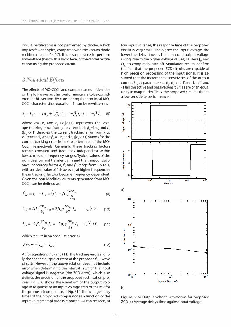
As for equations (10) and (11), the tracking errors slight-ly change the output current of the proposed full-wave circuits. However, the above relation does not include error when determining the interval in which the input voltage signal is negative (the ZCD error), which also defines the precision of the proposed rectification pro-cess. Fig. 5 a) shows the waveform of the output volt-age in response to an input voltage step of ±50mV for the proposed comparator. In Fig. 5 b), the average delay times of the proposed comparator as a function of the input voltage amplitude is reported. As can be seen, at
low input voltages, the response time of the proposed circuit is very small. The higher the input voltage, the lower the delay time, as the enhanced output voltage swing (due to the higher voltage values) causes Q19 and Q20 to completely turn-off. Simulation results confirm the fact that the proposed ZCD circuits are capable of high precision processing of the input signal. It is as-sumed that the incremental sensitivities of the output current iout at parameters α, βp, βn and T are: 1; 1; 1 and -1 (all the active and passive sensitivities are of an equal unity in magnitude). Thus, the proposed circuit exhibits a low sensitivity performance.
a)
b)
Figure 5: a) Output voltage waveforms for proposed ZCD, b) Average delays time against input voltage
P. B. Petrović; Informacije Midem, Vol. 46, No. 4(2016), 229 – 237

233
The error (12) is a function of input voltage signals and varies depending on its content. A way to express the error is to consider the values of the observed param-eters as random quantities characterized by their PDFs (Probability Density Function). Therefore, the interval having a 2e width, around the nominal value of the ob-served parameters needs to be defined and associated with a certain distribution, e.g. uniform distribution.
The Monte Carlo approach [24] gives the lower and up-per limits of interval which contains 95% of error sam-ples. The Monte Carlo analysis in PSpice was used for simulations with a given error on different parameters and components (Monte Carlo predicts the behaviour of a circuit statistically when part values are varied within their tolerance range by 5%), Fig. 6. This test is very useful for visualizing how a circuit runs with im-perfect parameters as are used in reality. The number of individual simulation was 2000.
Figure 6. The distribution of errors, for the divergence in the value of the parameters, from their nominal values
4 Simulation Results
To confirm the given theoretical analysis, the proposed voltage-mode bipolar full-wave circuit in Fig. 1 was simulated using the PSpice program. The MO-CCCII
and ZCD were realized by the schematic bipolar imple-mentations given in Figs. 3 and 4, with the transistor model parameters of PR200N (PNP) and NP200N (NPN) of the bipolar arrays ALA400 from AT&T [25], Table 1. The supply voltages and the values of the bias currents were +V=−V=1.2 V and IP=300 mA respectively, whereas the input voltage was within the range of ±100 mV. Parameters of National Semiconductor circuits AH510 [26] were used as analog current switch during simula-tion.
Table 1: PR200N and NP200N transistor parameters
Transistor type: NP200N.MODEL NX2 NPN RB = 262.5 IRB = 0 RBM = 12.5 RC = 25 RE = 0.5 IS = 242E - 18 EG = 1.206 XTI = 2 XTB =
1.538 BF = 137.5 IKF = 13.94E - 3 NF = 1.0 VAF = 159.4 ISE = 72E - 16 NE = 1.713 BR = 0.7258 IKR = 4.396E - 3 NR = 1.0 VAR = 10.73 ISC = 0 NC = 2 + TF = 0.425E - 9 TR = 0.425E - 8 CJE = 0.428E - 12 VJE = 0.5 MJE = 0.28 CJC = 1.97E - 13 VJC = 0.5 MJC = 0.3 XCJC = 0.065 CJS
= 1.17E - 12 VJS = 0.64 MJS = 0.4 FC = 0.5Transistor type: PR200N
.MODEL PX2 PNP RB = 163.5 IRB = 0 RBM = 12.27 RC = 25 RE = 1.5 IS = 147E - 18 EG = 1.206 XTI = 1.7 XTB = 1.866 BF = 110.0 IKF = 4.718E - 3 NF = 1 VAF = 51.8
ISE = 50.2E - 16 NE = 1.65 BR = 0.4745 IKR = 12.96E - 3 NR = 1 VAR = 9.96 ISC = 0 NC = 2 TF = 0.610E - 9 TR = 0.610E - 8 CJE = 0.36E - 12 VJE = 0.5 MJE = 0.28 CJC
= 0.328E - 12 VJC = 0.8 MJC = 0.4 XCJC = 0.074 CJS = 1.39E - 12 VJS = 0.55 MJS = 0.35 FC = 0.5
Time response of the proposed ZCD circuits is shown in Fig. 7, where the input voltage signal is of 1 MHz fre-quency and 20 mV peak. Resistor R1=1 kΩ was used in the simulation process. This clearly infers that the pro-posed solution detectors are able to sense polarity of the input voltage signal with high precision, whereby the error resulting from imprecision in detection is neg-ligible in practical applications.
The DC characteristic of the proposed circuit at a fre-quency of 1 MHz is shown in Fig. 8. Fig. 8 implies that
Figure 7: Time-domain response of proposed ZCD
P. B. Petrović; Informacije Midem, Vol. 46, No. 4(2016), 229 – 237
234
the proposed circuit retains a linear character in a wide voltage range.
Fig. 9 shows the wave form of the signal at the output of the circuit shown in Fig. 1 (voltage vout), at different frequencies. For these simulations, the input signal is taken as a sinusoidal voltage signal at 40 mV peak value, the selected frequencies ranging from 1 kHz to 10 MHz. Fig. 9 shows that the output waveform of the proposed rectifier is in a good agreement with the theoretical ones at low and high frequencies. However, the higher the frequency of the processed signal, the greater the deviations.
The total power dissipation was 2.83 mW. Low power con-sumption of the proposed circuits occurs due to the appli-cation of low-voltage current mode and transconductance mode integrated circuits, along with the use of bipolar tran-sistor technique. Applying the current mode signal pro-
cessing to solve the issues under consideration is a sensible approach to the problem. However, similar and sometimes lower power consumption can be achieved using CMOS technology instead of the bipolar one.
To test the tunability of the gain of the proposed rec-tifier circuit, the bias current of the MO-CCCI (IB) is changed and the results are shown in Fig. 10. For these simulations, the input signal is taken as a sinusoidal voltage signal with 100 kHz frequency and 50 mV peak value at a load of RL=100 Ω.
Figure 10: Tunability of the gain of the proposed recti-fier with changing the bias current IB a) IB=200 µA; b) IB=130 µA; c) IB=115 µA; d) IB=100 µA
4.1 Harmonic distortion
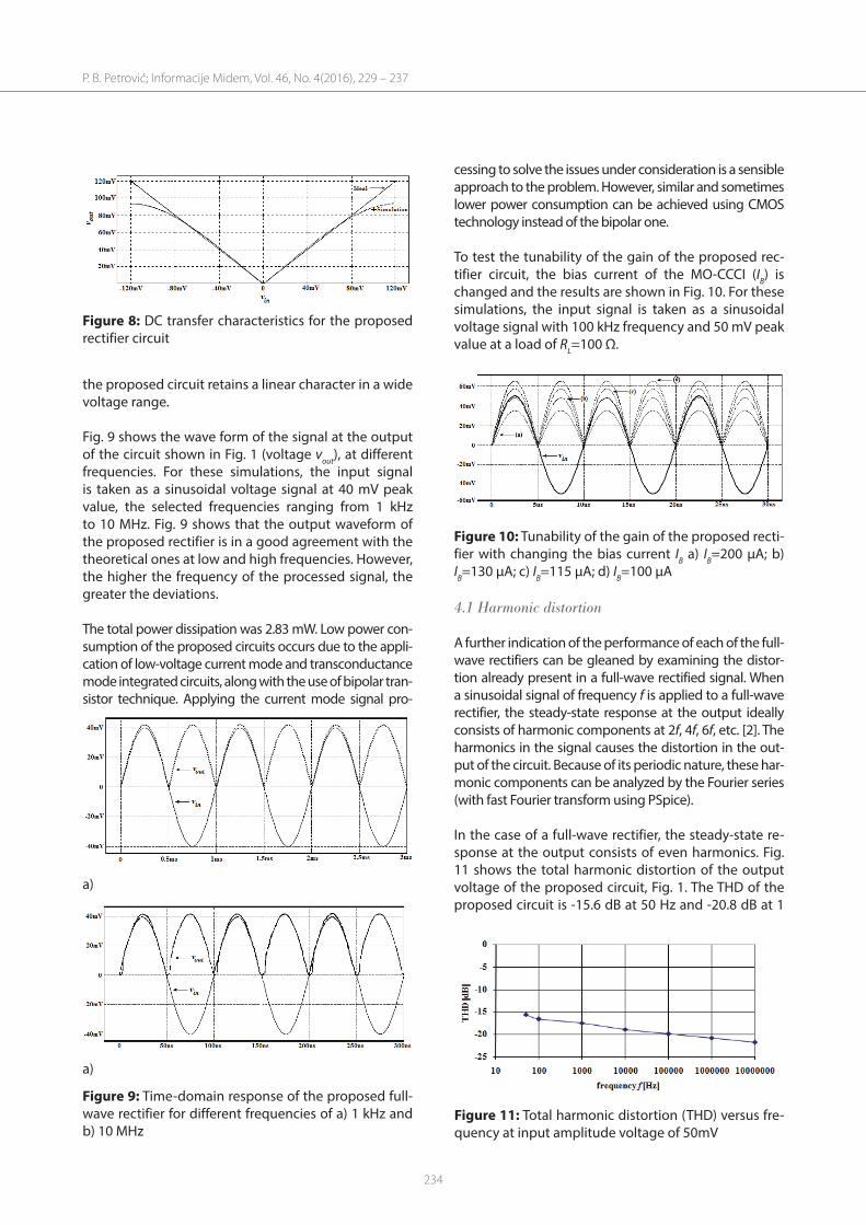
A further indication of the performance of each of the full-wave rectifiers can be gleaned by examining the distor-tion already present in a full-wave rectified signal. When a sinusoidal signal of frequency f is applied to a full-wave rectifier, the steady-state response at the output ideally consists of harmonic components at 2f, 4f, 6f, etc. [2]. The harmonics in the signal causes the distortion in the out-put of the circuit. Because of its periodic nature, these har-monic components can be analyzed by the Fourier series (with fast Fourier transform using PSpice).
In the case of a full-wave rectifier, the steady-state re-sponse at the output consists of even harmonics. Fig. 11 shows the total harmonic distortion of the output voltage of the proposed circuit, Fig. 1. The THD of the proposed circuit is -15.6 dB at 50 Hz and -20.8 dB at 1
Figure 8: DC transfer characteristics for the proposed rectifier circuit
Figure 9: Time-domain response of the proposed full-wave rectifier for different frequencies of a) 1 kHz and b) 10 MHz
a)
a)
P. B. Petrović; Informacije Midem, Vol. 46, No. 4(2016), 229 – 237
Figure 11: Total harmonic distortion (THD) versus fre-quency at input amplitude voltage of 50mV

235
MHz with an input signal of 50 mV. The THD is signifi-cantly lower than in [2], [27], [28] (the THD of previously reported circuit slowly increases with frequency), be-cause of higher frequency ranges, the diode switching ON and OFF tends to become sluggish due to its higher impendence and more distortions.
4.2 Comparison with the Existing Circuits
To gain a better insight into the technique proposed here, the performance of the proposed circuits was compared to the previous one implementing full-wave rectifiers. Table 2 summarizes this comparison by showing some important parameters of the rectifiers. It should be assumed here that not all of the comparison realizations rely on the concept of a voltage-mode cir-cuit, as is the one proposed in this paper.
The proposed rectifier requires fewer active components than the one described in [2], [22], [27], [31], along with lower THD of the output voltage and lower consump-tion. Additionally, the circuit described in this paper enables electronic control of the gain of the proposed rectifier circuit (amplitude of the output voltage signal).
5 Conclusion
In this paper, new full-wave rectifier topologies are given. The circuit employs only two active components
Table 2: Comparison of performance of different rectifiers
Ref. Type of active building blocks used
Number of diodes
Number of resistors
Auxiliary bias sources
Maximum frequency Maximum amplitude
Power consumption
[2] 4 CCCII, 3 MOS - - yes 20 MHz ±1 V 9.43 mW[6] 1 CCCII, 2 MOS - 1 no 100 kHz ±10 mV -
[12] 2 CCIIs, 3 MOS - - no 22 MHz ±50 mV -[13] 1 DXCCII, 3MOS - - yes 10 MHz ±150 mV 3.33 mW[14] 2 CCIIs 4 2 no 10 kHz 3 V -[15] 1 CCIIs, 1 UVCs 2 - no 500 kHz ±200 mA 1.19 mW[16] 1 CCIIs, 1 UVCs 2 - yes 1 MHz ±300 mV -[17] 1 CDTAs 4 1 no 10 MHz ±1 mA -[20] 1 CDTAs 2 1 no Variable up to 42 MHz ±5 mA -[21] 1 DXCCIIs 2 1 no 1 MHz ±500 mV -[22] 1 MZC-CDTA, 2 MOS - - no 10 MHz ±300 mA 14 mW[27] 3OA, 3 AD633/AD 1 9 no 1 MHz ±5 V -[28] 3 CCCII - 5 yes 5 MHz ±500 mV -[29] 1 OTA/1 DVCC 2 2/3 no 1 MHz ±200 mA -[30] 1 CDTA 4 - yes 1 GHz ±210 µA 6.31 mW[31] 1 CCII, 1 DXCCII 2 2 no 1 MHz ±350 mV -[32] 47 MOS, 9 CS - 1 no 100 MHz ±200 mV 5.2 mW[33] 2 CCII 2 3 yes 10 MHz ±1 V -
This work 1 DOCCCIIs, ZCD, 2 MOS - 1 no 10 MHz ±100 mV 2.83 mW
and one resistor operating in VM, which is advanta-geous from the integration point of view. The perfor-mance of the proposed circuits is demonstrated by PSpice simulations using the bipolar arrays ALA400 from AT&T technology parameters. The effects of the non-idealities of the active elements are also investi-gated. The proposed circuit has a high precision and linearity, low power consumption and wide bandwidth.
6 References
1. R. B. Northrop, “Analog Electronics Circuits”, Read-ing, MA: Addison-Wesley, 1990.
2. P. B. Petrović, “A new tunable current-mode peak detector,” Microelectronics Journal, vol. 45, no 6, pp. 805–814, 2014. doi: 10.1016/j.mejo.2014.02.019
3. P. B. Petrović, “A New Peak Detector Based on Us-age of CCCIIs,” in Proceedings of Advances in Instru-mentation and Sensors Interoperability. 19th IM-EKO TC 4 Symposium and 17th IWADC Workshop, Barcelona, Spain, 2013.
4. A. Fabre, O. Saaid, F. Wiest, C. Bouchheron, “Cur-rent controllable bandpass filter based on trans-linear conveyors,” Electron. Lett., vol. 31, pp. 1727-1728, 1995. doi: 10.1049/el:19951225
5. S.J. Gift, “A high-performance full-wave rectifier circuit,” Int. J. Electron., vol. 87, no. 8, pp. 925-930, 2000. doi: 10.1080/002072100404587
P. B. Petrović; Informacije Midem, Vol. 46, No. 4(2016), 229 – 237

236
6. S. Maheshwari, “Current controlled precision rectifier circuits,” Journal of Circuits, Systems, and Computers, vol. 16, no. 1, pp. 129-138, 2007. doi: 10.1142/S0218126607003496
7. A.A. Khan, M.A. El-ela, M. A. Al-Turaigi,. “Cur-rent-mode precision rectification,” Int. J. Elec-tron., vol. 79, no. 6, pp. 853-859, 1995. doi: 10.1080/00207219508926319
8. B. Wilson, V. Mannama, “Current-mode rectifier with improved precision,” Electron. Lett., vol. 31, no. 4, pp. 247-248, 1995. doi: 10.1049/el:19950185
9. J. R. Angulo, R. G. Carvajal, J. M. Hereida, A. Tor-rabla, “Very Low-Voltage Class AB CMOS Precision Voltage and Current Rectifier,” in Proceedings of IEEE Intern. Sym.on Cir.and Sys., pp. III-5¸III-8, 2000. doi: 10.1109/ISCAS.2000.855981
10. A. V. Garcia, R. Venkatasubramanian, J.S. Martinez, E.S. Sinencio, “A Broadband CMOS Amplitude De-tector for On-Chip RF Measurements,” IEEE Trans. Instrum. Meas., vol. 57, no. 7, pp. 1470-1477, 2008. doi: 10.1109/TIM.2008.917196
11. C. Peters, J. Handwerker, D. Maurath, Y. Manoli, “A Sub-500 mV Highly Efficient Active Rectifier for Energy Harvesting Applications,” IEEE Trans. Cir. Sys.-I, vol. 58, no. 7, pp. 1542-1550, 2011. doi: 10.1109/TCSI.2011.2157739
12. E. Yuce, S. Minaei, O. Çicekoglu, “Full-wave rectifier realization using only two CCII+s and NMOS tran-sistors,” Int. J. Electron., vol. 93, no. 8, pp. 533–541, 2006. doi: 10.1080/00207210600711606
13. S. Minaei, E. Yuce, “A new full-wave rectifier circuit employing single dual-X current conveyor,” Int. J. Electron., vol. 95, no. 8, pp. 777–784, 2008. doi: 10.1080/00207210802141826
14. C. Toumayou, F. J. Lidgey, S. Chattong, “High fre-quency current conveyor precision full-wave rec-tifier,” Electron. Lett., vol. 30, no. 10, pp. 745–746, 1994. doi: 10.1049/el:19940539
15. J. Koton, N. Herencsar, K. Vrba, “Minimal configu-ration precision full-wave rectifier using current and voltage conveyors,” IEICE Electron. Express, no. 7–12, pp. 844–849, 2010. doi:10.1587/elex.7.844
16. J. Koton, N. Herencsar, K. Vrba, “Current and volt-age conveyors in current and voltage-mode pre-cision full-wave rectifiers,” Radioengineering, vol. 20, no. 1, pp. 19–24, 2011.
17. J. Koton, N. Herencsar, K. Vrba, S. Minaei, “Precision full-wave current-mode rectifier using current dif-ferencing transconductance amplifier,” in Proc. of 2011 Int. Conf. on Computer and Communication Devices (ICCCD 2011), Bali Island, Indonesia, pp. 71–74, 2011. doi: 10.1109/ICCSN.2011.6014935
18. S. Hashemi M. Sawan, Y. Savaria, “A novel low-drop CMOS active rectifier for RF-powered devices: experimental results,” Microelectron. Journal, vol.
40, no. 11, pp. 1547–1554, 2009. doi: 10.1016/j.mejo.2009.02.007
19. M. Kumngern, “CMOS current-mode preci-sion full-wave rectifier with improved band-width,” Second Int. Conf. on Digital Information and Communication Technology and its Applica-tions (DICTAP), pp. 283–286, 2012. doi: 10.1109/DICTAP.2012.6215357
20. F. Khateb J. Vavra, D. Biolek, “A novel current-mode full-wave rectifier based on one CDTA and two diodes,” Radioengineering, vol. 19, no. 3, pp. 437–445, 2010.
21. J. Koton, N. Herencsar, K. Vrba, “Current-mode precision full-wave rectifier using single DXCCII and two diodes,” 20th European Conf. Circuit The-ory and Design (ECCTD), pp. 508–511, 2011. doi: 10.1109/ECCTD.2011.6043400
22. N. Pandey, R. Pandey, “Current mode full-wave rectifier based on a single MZC-CDTA,” Act. Pas-siv. Electron. Compon., Article ID 967057, pp. 1–5, 2013. doi: 10.1155/2013/967057
23. W. Tangsrirat, “Current-tunable current-mode multifunction filter based on dual-output cur-rent-controlled conveyors,” AEÜ-Int. J. Electron. Commun., vol. 61, no. 8, pp. 528–533, 2007. doi: 10.1016/j.aeue.2006.09.005
24. Evaluation of measurement data — Supplement 1 to the “Guide to the expression of uncertainty in measurement” - Propagation of distributions us-ing a Monte Carlo method, BIPM, 2008.
25. D. R. Frey, “Log-domain filtering: an approach to current mode filtering,” IEE Proc Circuit Devices Syst., vol. 140, pp. 406–416, 1993. doi: 10.1049/ip-g-2.1993.0066
26. AH5010/AH5011/AH5012 Monolithic Analog Current Switches, National Semiconductor, data sheet, 1995.
27. P.P. Sahu, M. Singh, A. Baishya, “A Novel Versatile Precision Full-Wave Rectifier,” IEEE Trans. Instrum. Meas., vol. 59, no. 10, pp. 2742-2746, 2010. doi: 10.1109/TIM.2010.2045539
28. K. Anuntahirunrat, W. Tangsrirat, V. Riewru-ja, W. Surakampontor, “Sinusoidal frequency doubler and full-wave rectifier using translin-ear current controlled conveyors,” Int. J. Elec-tronics, vol. 91, no. 4, pp. 227–239, 2004. doi: 10.1080/00207210410001690656
29. M. Sagbas, S. Minaei, U. E. Ayten, “Component reduced current-mode full-wave rectifier cir-cuits using single active component,” IET Circuits, Devices&Systems, vol. 10, no. 1, pp. 1–11, 2016. doi: 10.1049/iet-cds.2013.0461
30. D. Biolek, E. Hancioglu, A.U. Keskin, “High-perfor-mance current differencing transconductance amplifier and its application in precision current-mode rectification,” AEÜ-Int. J. Electron. Commun.,
P. B. Petrović; Informacije Midem, Vol. 46, No. 4(2016), 229 – 237

237
vol. 62, no. 2, pp. 92–96, 2008. doi: 10.1016/j.aeue.2007.03.003
31. J. Koton, K. Vrba, N. Herencsar, “Fast voltage-mode full-wave rectifier using CCII and DXCCII,” Eighth Int. Conf. on Electrical and Electronics Engineering (ELECO 2013), Bursa, Turkey, pp. 49–52, 2013. doi: 10.1109/ELECO.2013.6713934
32. M. Kumngern, “New versatile precision rectifier,” IET Circuits Devices&Systems, vol. 8, no. 2, pp. 141–151, 2014. doi: 10.1049/iet-cds.2013.0232
33. A. Monpapassorn, “Low output imped-ance dual CCII full-wave rectifier,” Int. J. Elec-tron., vol. 100, no. 5, pp.648–654, 2013. doi: 10.1080/00207217.2012.720943
Arrived: 19. 08. 2016Accepted: 28. 09. 2016
P. B. Petrović; Informacije Midem, Vol. 46, No. 4(2016), 229 – 237