vtt’s micron-scale silicon photonics platform · vtt’s micron-scale silicon photonics platform...
TRANSCRIPT
VTT’s micron-scale silicon
photonics platform
Timo Aalto
VTT Technical Research Centre of Finland
PIC training in NY, October 2015

2 2
Outline
What means ”Thick SOI” or ”Micron-scale silicon photonics” ?
Introduction to VTT’s SOI technology and the Micronova fab
Basics of rib and strip waveguides in Thick-SOI
3 µm and 12 µm SOI platforms (incl. interposers)
Design support and access in Thick-SOI
Comparison between different SOI technologies
3 3
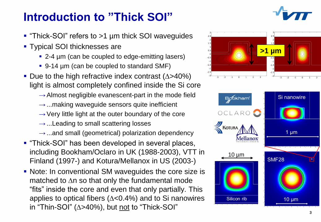
Introduction to ”Thick SOI”
“Thick-SOI” refers to >1 µm thick SOI waveguides
Typical SOI thicknesses are
2-4 µm (can be coupled to edge-emitting lasers)
9-14 µm (can be coupled to standard SMF)
Due to the high refractive index contrast (>40%)
light is almost completely confined inside the Si core
→ Almost negligible evanescent-part in the mode field
→ ...making waveguide sensors quite inefficient
→ Very little light at the outer boundary of the core
→ ...Leading to small scattering losses
→ ...and small (geometrical) polarization dependency
“Thick-SOI” has been developed in several places,
including Bookham/Oclaro in UK (1988-2003), VTT in
Finland (1997-) and Kotura/Mellanox in US (2003-)
Note: In conventional SM waveguides the core size is
matched to n so that only the fundamental mode
“fits” inside the core and even that only partially. This
applies to optical fibers (<0.4%) and to Si nanowires
in “Thin-SOI” (>40%), but not to “Thick-SOI”
>1 µm
10 µm
4
Introduction to
VTT’s SOI technology
and the Micronova fab
5 5
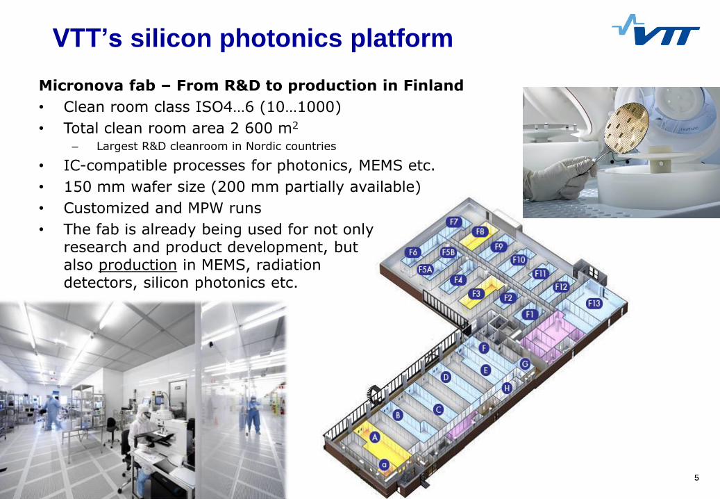
Micronova fab – From R&D to production in Finland
• Clean room class ISO4…6 (10…1000)
• Total clean room area 2 600 m2
– Largest R&D cleanroom in Nordic countries
• IC-compatible processes for photonics, MEMS etc.
• 150 mm wafer size (200 mm partially available)
• Customized and MPW runs
• The fab is already being used for not only research and product development, but also production in MEMS, radiation detectors, silicon photonics etc.
VTT’s silicon photonics platform
6 6
Oulu
Espoo
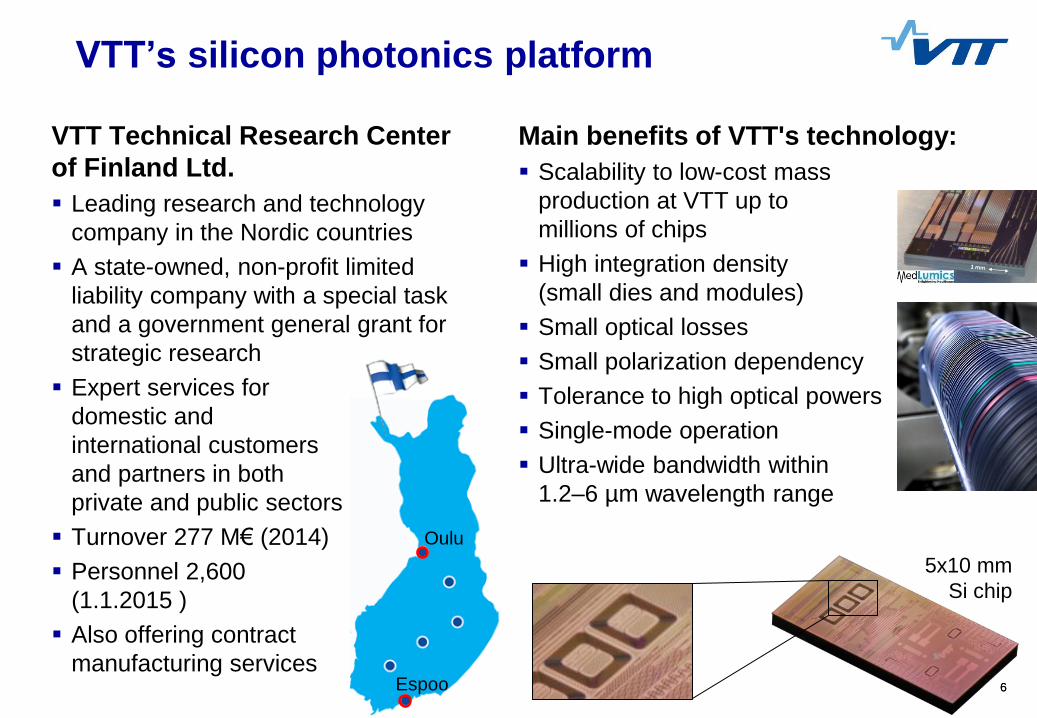
VTT’s silicon photonics platform
VTT Technical Research Center
of Finland Ltd.
Leading research and technology
company in the Nordic countries
A state-owned, non-profit limited
liability company with a special task
and a government general grant for
strategic research
Expert services for
domestic and
international customers
and partners in both
private and public sectors
Turnover 277 M€ (2014)
Personnel 2,600
(1.1.2015 )
Also offering contract
manufacturing services
Main benefits of VTT's technology:
Scalability to low-cost mass
production at VTT up to
millions of chips
High integration density
(small dies and modules)
Small optical losses
Small polarization dependency
Tolerance to high optical powers
Single-mode operation
Ultra-wide bandwidth within
1.2–6 µm wavelength range
5x10 mm
Si chip
7 7
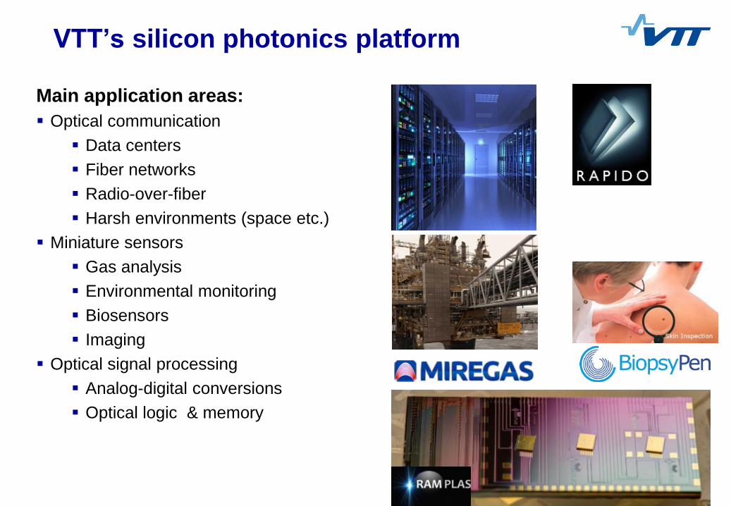
VTT’s silicon photonics platform
Main application areas:
Optical communication
Data centers
Fiber networks
Radio-over-fiber
Harsh environments (space etc.)
Miniature sensors
Gas analysis
Environmental monitoring
Biosensors
Imaging
Optical signal processing
Analog-digital conversions
Optical logic & memory
8
Basics of rib and strip
waveguides in Thick-SOI

9 9
Basics of rib waveguides
Wavelength independent SM operation (1.2 µm < λ < 6 µm)
when the following three rules apply:
Width limit:
Height ratio limit: h ≥ H/2
Absolute size: H ≥ 2λ
Benefits:
Small propagation loss (0.1 dB/cm)
Small birefringency (Δneff ~10-3)
SM operation over ultra-wide bandwidth
Limitations:
Low horizontal index contrast, leading to
large bending radius (mm/cm scale)
Cross-talk between waveguides
H h
W
10 10
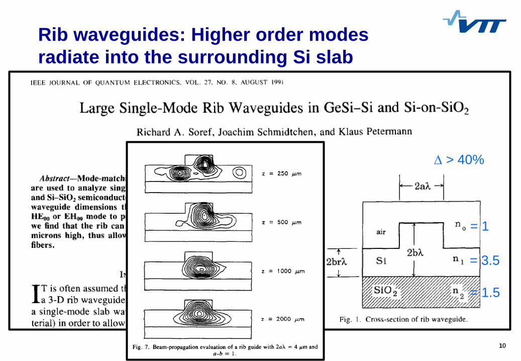
Rib waveguides: Higher order modes
radiate into the surrounding Si slab
= 1
= 3.5
= 1.5
> 40%

11 11
Basics of strip waveguides
Highly multi-moded waveguides
Can be used in SM waveguide circuits IF the unwanted
excitation of higher order modes is prevented and light is kept
in the fundamental mode
Adiabatic rib-strip converters are a key component
Benefits:
Small propagation loss (0.1-0.15 dB/cm)
Zero birefringence possible by tuning the aspect ratio
Euler bends reaching down to 1 µm bending radius
No cross-talk between waveguides, even in dense arrays
Limitations:
Risk of exciting higher-order modes and causing modal
interference

12 12
Euler bends: How to reduce
bending radius by x1000?
Reff = 1.3 µm
Rmin = 0.9 µm
Loss < 0.1 dB/90°
Adopting Euler bends from civil engineering to
waveguide optics
Thick-SOI waveguides allow µm-size bends if
mode excitation is properly well-controlled
0
1
2
-1
-2
0 1 2 3 4
13
3 µm and 12 µm
SOI platforms
(incl. interposers)
14 14
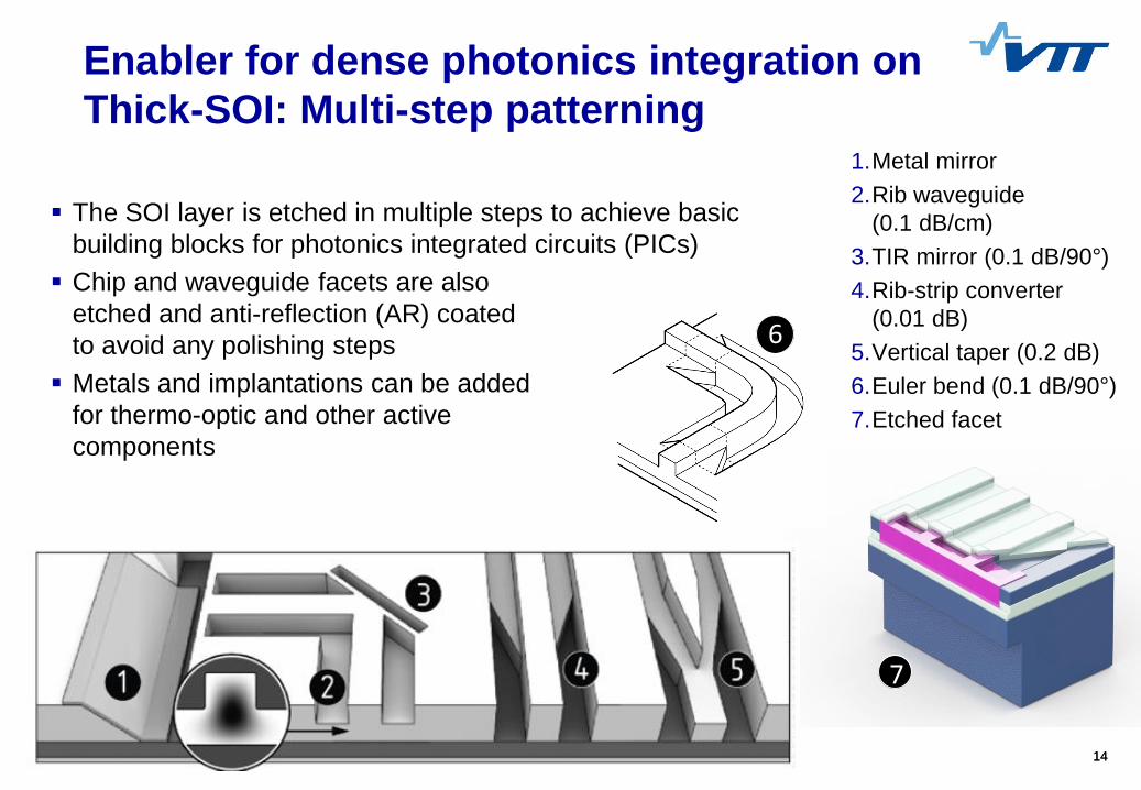
Enabler for dense photonics integration on
Thick-SOI: Multi-step patterning 1.Metal mirror
2.Rib waveguide
(0.1 dB/cm)
3.TIR mirror (0.1 dB/90°)
4.Rib-strip converter
(0.01 dB)
5.Vertical taper (0.2 dB)
6.Euler bend (0.1 dB/90°)
7.Etched facet
6
The SOI layer is etched in multiple steps to achieve basic
building blocks for photonics integrated circuits (PICs)
Chip and waveguide facets are also
etched and anti-reflection (AR) coated
to avoid any polishing steps
Metals and implantations can be added
for thermo-optic and other active
components
7
15 15
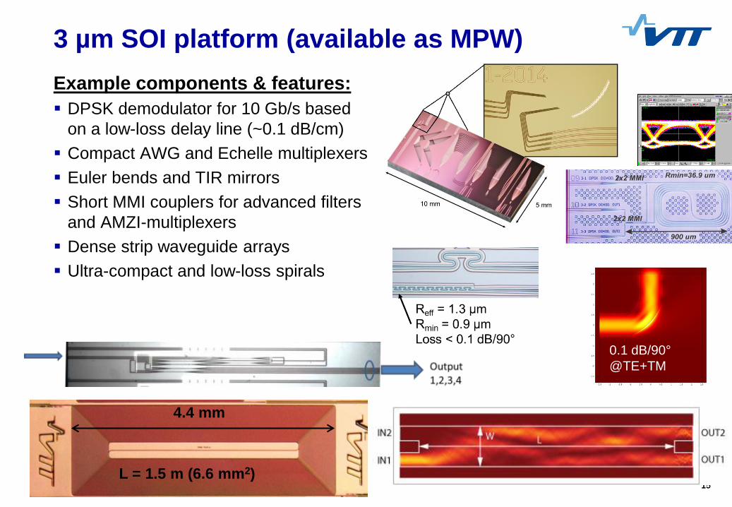
3 µm SOI platform (available as MPW)
Example components & features:
DPSK demodulator for 10 Gb/s based
on a low-loss delay line (~0.1 dB/cm)
Compact AWG and Echelle multiplexers
Euler bends and TIR mirrors
Short MMI couplers for advanced filters
and AMZI-multiplexers
Dense strip waveguide arrays
Ultra-compact and low-loss spirals
0.1 dB/90°
@TE+TM
4.4 mm
L = 1.5 m (6.6 mm2)
16 16
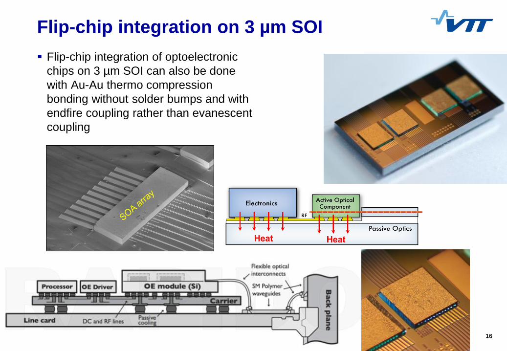
Flip-chip integration on 3 µm SOI
Flip-chip integration of optoelectronic
chips on 3 µm SOI can also be done
with Au-Au thermo compression
bonding without solder bumps and with
endfire coupling rather than evanescent
coupling
17 17
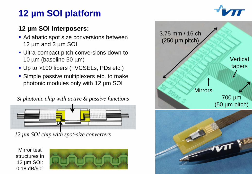
12 µm SOI platform
Si photonic chip with active & passive functions
12 µm SOI chip with spot-size converters
12 µm SOI interposers:
Adiabatic spot size conversions between
12 µm and 3 µm SOI
Ultra-compact pitch conversions down to
10 µm (baseline 50 µm)
Up to >100 fibers (+VCSELs, PDs etc.)
Simple passive multiplexers etc. to make
photonic modules only with 12 µm SOI
3.75 mm / 16 ch
(250 µm pitch)
700 µm
(50 µm pitch)
Vertical
tapers
Mirrors
Mirror test
structures in
12 µm SOI:
0.18 dB/90°
18 18
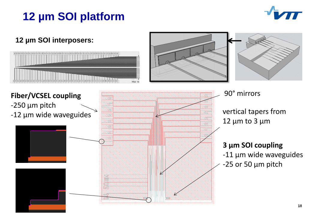
12 µm SOI platform
12 µm SOI interposers:
Fiber/VCSEL coupling -250 µm pitch -12 µm wide waveguides
90° mirrors
vertical tapers from 12 µm to 3 µm
3 µm SOI coupling -11 µm wide waveguides -25 or 50 µm pitch
19 19
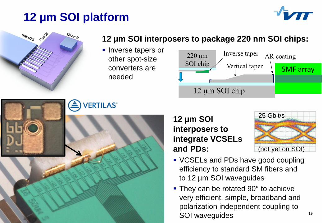
12 µm SOI platform
12 µm SOI interposers to package 220 nm SOI chips:
Inverse tapers or
other spot-size
converters are
needed
12 µm SOI
interposers to
integrate VCSELs
and PDs:
VCSELs and PDs have good coupling
efficiency to standard SM fibers and
to 12 µm SOI waveguides
They can be rotated 90° to achieve
very efficient, simple, broadband and
polarization independent coupling to
SOI waveguides
25 Gbit/s
(not yet on SOI)
20
Design support and
access in Thick-SOI
21 21
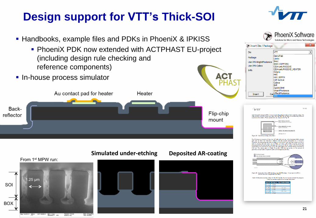
Design support for VTT’s Thick-SOI
Handbooks, example files and PDKs in PhoeniX & IPKISS
PhoeniX PDK now extended with ACTPHAST EU-project
(including design rule checking and
reference components)
In-house process simulator
Simulated under-etching Deposited AR-coating
22 22
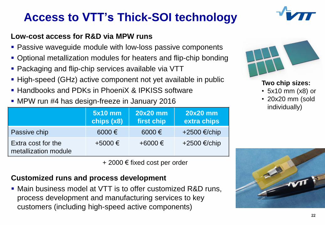
Access to VTT’s Thick-SOI technology
Low-cost access for R&D via MPW runs
Passive waveguide module with low-loss passive components
Optional metallization modules for heaters and flip-chip bonding
Packaging and flip-chip services available via VTT
High-speed (GHz) active component not yet available in public
Handbooks and PDKs in PhoeniX & IPKISS software
MPW run #4 has design-freeze in January 2016
Customized runs and process development
Main business model at VTT is to offer customized R&D runs,
process development and manufacturing services to key
customers (including high-speed active components)
Two chip sizes:
• 5x10 mm (x8) or
• 20x20 mm (sold
individually) 5x10 mm
chips (x8)
20x20 mm
first chip
20x20 mm
extra chips
Passive chip 6000 € 6000 € +2500 €/chip
Extra cost for the
metallization module
+5000 € +6000 € +2500 €/chip
+ 2000 € fixed cost per order
23 23
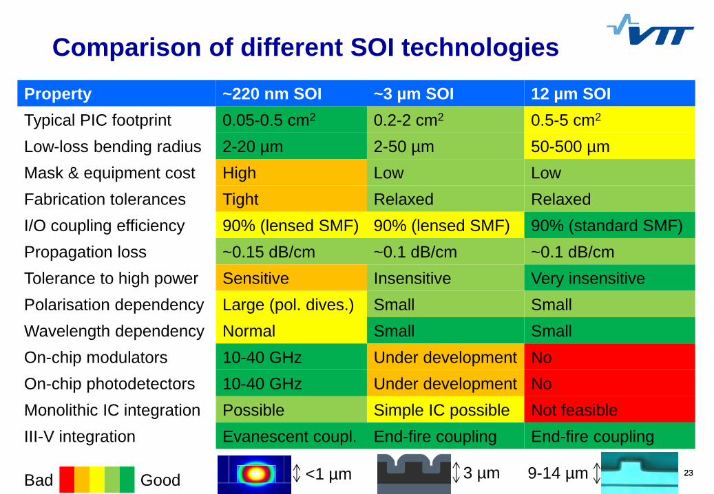
Comparison of different SOI technologies
Property ~220 nm SOI ~3 µm SOI 12 µm SOI
Typical PIC footprint 0.05-0.5 cm2 0.2-2 cm2 0.5-5 cm2
Low-loss bending radius 2-20 µm 2-50 µm 50-500 µm
Mask & equipment cost High Low Low
Fabrication tolerances Tight Relaxed Relaxed
I/O coupling efficiency 90% (lensed SMF) 90% (lensed SMF) 90% (standard SMF)
Propagation loss ~0.15 dB/cm ~0.1 dB/cm ~0.1 dB/cm
Tolerance to high power Sensitive Insensitive Very insensitive
Polarisation dependency Large (pol. dives.) Small Small
Wavelength dependency Normal Small Small
On-chip modulators 10-40 GHz Under development No
On-chip photodetectors 10-40 GHz Under development No
Monolithic IC integration Possible Simple IC possible Not feasible
III-V integration Evanescent coupl. End-fire coupling End-fire coupling
Bad Good 9-14 µm 3 µm <1 µm