w-cdma/w-tdd/td-scdma zero-if receivers · pdf filegeneral description the...
TRANSCRIPT
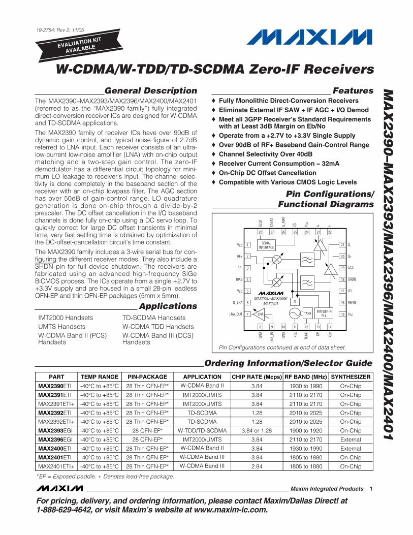
General DescriptionThe MAX2390–MAX2393/MAX2396/MAX2400/MAX2401(referred to as the “MAX2390 family”) fully integrateddirect-conversion receiver ICs are designed for W-CDMAand TD-SCDMA applications.
The MAX2390 family of receiver ICs have over 90dB ofdynamic gain control, and typical noise figure of 2.7dBreferred to LNA input. Each receiver consists of an ultra-low-current low-noise amplifier (LNA) with on-chip outputmatching and a two-step gain control. The zero-IFdemodulator has a differential circuit topology for mini-mum LO leakage to receiver’s input. The channel selec-tivity is done completely in the baseband section of thereceiver with an on-chip lowpass filter. The AGC sectionhas over 50dB of gain-control range. LO quadrature generation is done on-chip through a divide-by-2prescaler. The DC offset cancellation in the I/Q basebandchannels is done fully on-chip using a DC servo loop. Toquickly correct for large DC offset transients in minimaltime, very fast settling time is obtained by optimization ofthe DC-offset-cancellation circuit’s time constant.
The MAX2390 family includes a 3-wire serial bus for con-figuring the different receiver modes. They also include aSHDN pin for full device shutdown. The receivers arefabricated using an advanced high-frequency SiGeBiCMOS process. The ICs operate from a single +2.7V to+3.3V supply and are housed in a small 28-pin leadlessQFN-EP and thin QFN-EP packages (5mm x 5mm).
Applications
Features♦ Fully Monolithic Direct-Conversion Receivers♦ Eliminate External IF SAW + IF AGC + I/Q Demod♦ Meet all 3GPP Receiver’s Standard Requirements
with at Least 3dB Margin on Eb/No♦ Operate from a +2.7V to +3.3V Single Supply♦ Over 90dB of RF+ Baseband Gain-Control Range♦ Channel Selectivity Over 40dB♦ Receiver Current Consumption ≈ 32mA♦ On-Chip DC Offset Cancellation♦ Compatible with Various CMOS Logic Levels
MA
X2
39
0–M
AX
23
93
/MA
X2
39
6/M
AX
24
00
/MA
X2
40
1
W-CDMA/W-TDD/TD-SCDMA Zero-IF Receivers
________________________________________________________________ Maxim Integrated Products 1
Ordering Information/Selector Guide
19-2754; Rev 2; 11/05
For pricing, delivery, and ordering information, please contact Maxim/Dallas Direct! at 1-888-629-4642, or visit Maxim’s website at www.maxim-ic.com.
EVALUATION KIT
AVAILABLE
*EP = Exposed paddle. + Denotes lead-free package.
PART TEMP RANGE PIN-PACKAGE APPLICATION CHIP RATE (Mcps) RF BAND (MHz) SYNTHESIZER
MAX2390ETI -40°C to +85°C 28 Thin QFN-EP* W-CDMA Band II 3.84 1930 to 1990 On-Chip
MAX2391ETI -40°C to +85°C 28 Thin QFN-EP* IMT2000/UMTS 3.84 2110 to 2170 On-Chip
MAX2391ETI+ -40°C to +85°C 28 Thin QFN-EP* IMT2000/UMTS 3.84 2110 to 2170 On-Chip
MAX2392ETI -40°C to +85°C 28 Thin QFN-EP* TD-SCDMA 1.28 2010 to 2025 On-Chip
MAX2392ETI+ -40°C to +85°C 28 Thin QFN-EP* TD-SCDMA 1.28 2010 to 2025 On-Chip
MAX2393EGI -40°C to +85°C 28 QFN-EP* W-TDD/TD-SCDMA 3.84 or 1.28 1900 to 1920 On-Chip
MAX2396EGI -40°C to +85°C 28 QFN-EP* IMT2000/UMTS 3.84 2110 to 2170 External
MAX2400ETI -40°C to +85°C 28 Thin QFN-EP* W-CDMA Band II 3.84 1930 to 1990 External
MAX2401ETI -40°C to +85°C 28 Thin QFN-EP* W-CDMA Band III 3.84 1805 to 1880 On-Chip
MAX2401ETI+ -40°C to +85°C 28 Thin QFN-EP* W-CDMA Band III 2.84 1805 to 1880 On-Chip
Pin Configurations/Functional Diagrams
28 27 26
21
20
19
1
2
3
184
17
16
5
6
157
25 24 23 22
8 9 10 11 12 13 14
Q-
Q+
AGC
SHDN
LD
REFIN
VCC
VCC
RF+
RF-
BIAS
VCC
G_LNA
LNA_OUT TANK
SCLK
SDAT
A
G_M
XR
I+ I-CS V CC
GND
LNA_
IN
GND CP V CC
V CC
TUNE
MAX2390–MAX2393/MAX2401
INTEGER-NPLL
SERIALINTERFACE
/2
LNAIMT2000 HandsetsUMTS HandsetsW-CDMA Band II (PCS)Handsets
TD-SCDMA HandsetsW-CDMA TDD HandsetsW-CDMA Band III (DCS)Handsets
Pin Configurations continued at end of data sheet.

MA
X2
39
0–M
AX
23
93
/MA
X2
39
6/M
AX
24
00
/MA
X2
40
1
W-CDMA/W-TDD/TD-SCDMA Zero-IF Receivers
2 _______________________________________________________________________________________
ABSOLUTE MAXIMUM RATINGS
DC ELECTRICAL CHARACTERISTICS(VCC = 2.7V to 3.3V, VSHDN = VDH (Note 1), G_LNA = G_MXR = VIH, HGML mode (see Table 6), no RF input signals, RF input andoutput ports are terminated into 50Ω, baseband I and Q outputs loaded with 10kΩ || 5pF, VAGC = 2.2V, TA = -40°C to +85°C. Typicalvalues are for VCC = 2.8V, TA = +25°C, unless otherwise noted.)
Stresses beyond those listed under “Absolute Maximum Ratings” may cause permanent damage to the device. These are stress ratings only, and functionaloperation of the device at these or any other conditions beyond those indicated in the operational sections of the specifications is not implied. Exposure toabsolute maximum rating conditions for extended periods may affect device reliability.
VCC to GND...........................................................-0.3V to +3.6VAll Other Pins to GND.................................-0.3V to (VCC + 0.3V)LNA_IN ...........................................................................+15dBmDigital Input Current .........................................................±10mADigital Output Open-Collector Current .................................1mAContinuous Power Dissipation (TA = +70°C)
28-Pin QFN (derate 20.8mW/°C above +70°C) ......1666.7mW
Operating Temperature Range ...........................-40°C to +85°CJunction Temperature ......................................................+150°CStorage Temperature Range .............................-65°C to +160°CLead Temperature (soldering, 10s) .................................+300°C
PARAMETER SYMBOL CONDITIONS MIN TYP MAX UNITS
Supply Voltage VCC 2.7 2.8 3.3 V
HGML mode 33 39
HGHL mode 34 40
LG mode 29 35MAX2391, MAX2392,MAX2393, MAX2400
IDLE mode 11.5 13
HGML mode 31 38
LG mode 27 34MAX2396
IDLE mode 10.5 12
HGML mode 35 42
HGHL mode 36 43
LG mode 31 37MAX2390, MAX2401
IDLE mode 12 14
mAOperating Supply Current ICC
All versions SHDN mode 0.5 15 µA
0.3V ≤ VAGC ≤ 2.4V -10 +10Gain-Control Input Bias Current IAGC
VAGC ≤ 0.3V; V SHDN = VDL 3µA
(VCM = 0 inOPCTRL register)
1.10 1.20 1.30Common-Mode Output Voltageat I and Q Outputs
VCMVI(CM) = (VI+ + VI-) / 2,VQ(CM) = (VQ+ + VQ-) / 2 (VCM = 1 in
OPCTRL register)1.30 1.42 1.55
V
Lock Indicator High LeakageCurrent
PLL locked, VLD = VCC(MAX2390–MAX2393, MAX2401)
0.1 µA
Lock Indicator Low SinkVoltage
Sinking 100µA, PLL unlocked(MAX2390–MAX2393, MAX2401)
0.4 V
MAX2390–MAX2393, MAX2401 1.5 VCCSHDN Input-Logic High VDH
MAX2396/MAX2400 VCC - 0.5 VCCV
SHDN Input-Logic Low VDL 0 0.5 V
SHDN Input Resistance Resistance to GND 50 kΩ
CAUTION! ESD SENSITIVE DEVICE

MA
X2
39
0–M
AX
23
93
/MA
X2
39
6/M
AX
24
00
/MA
X2
40
1
W-CDMA/W-TDD/TD-SCDMA Zero-IF Receivers
_______________________________________________________________________________________ 3
DC ELECTRICAL CHARACTERISTICS (continued)(VCC = 2.7V to 3.3V, VSHDN = VDH (Note 1), G_LNA = G_MXR = VIH, HGML mode (see Table 6), no RF input signals, RF input andoutput ports are terminated into 50Ω, baseband I and Q outputs loaded with 10kΩ || 5pF, VAGC = 2.2V, TA = -40°C to +85°C. Typicalvalues are for VCC = 2.8V, TA = +25°C, unless otherwise noted.)
PARAMETER SYMBOL CONDITIONS MIN TYP MAX UNITS
IDLE Input-Logic High VIH VCC - 0.5 VCC V
IDLE Input-Logic Low VIL 0 0.5 V
IDLE Input Resistance
MAX2396,MAX2400 only
Resistance to GND 50 kΩ
Digital Input-Logic High VIH
0.7 × VDH or1.2V, whicheveris greater
VCC
Digital Input-Logic Low VIL 0 0.3 × VDH
V
Input-Logic High Current IIH 1 µA
Input-Logic Low Current IIL
CS, SDATA, SCLK, G_MXR, G_LNA (Note 1)
-1 µA
AC ELECTRICAL CHARACTERISTICS(Devices tested on their respective evaluation kits (EV kits); LNA input port is driven with a 50Ω source; LNA output port is terminatedwith 50Ω load, mixer differential input port is driven through a 1:4 impedance balun with a 50Ω source; baseband I/Q output differentialload = 10kΩ || 5pF; reference oscillator input: 19.2MHz (MAX2390/MAX2391/MAX2392/MAX2393), 26MHz (MAX2401), 15.36MHz(MAX2396/MAX2400); AGC is set to result in a 0.3VP-P differential output-voltage swing at the baseband I/Q output; registers set topower-up defaults (Table 2); TA = -40°C to +85°C. Typical values are for VCC = 2.8V and TA = +25°C, unless otherwise noted.)
PARAMETER SYMBOL CONDITIONS MIN TYP MAX UNITS
LNA PERFORMANCE
MAX2391/MAX2396 2110 2140 2170
MAX2392 2010 2017 2025
MAX2393 1900 1910 1920
MAX2390/MAX2400 1930 1960 1990
RF Frequency Range (Note 2) fRF
MAX2401 1805 1842 1880
MHz
Signal Phase Change ∆φ Switching between any of the LNA modes 8 D eg r ees
LNA HIGH GAIN (“HGLNA”, G_LNA = VIH)
Power Gain GLNA (Note 3) 13 16 18 dB
Noise Figure NFLNA (Note 3) 1.5 2.0 dB
Input -1dB Compression Point IP-1dB (Note 3) -20 -16 dBm
MAX2391/MAX2396 -4.5 -2.5
MAX2392/MAX2393 -6 -43rd-Order Input Intercept Point(Note 4)
IIP3LNA
MAX2390/MAX2400/MAX2401 -7 -4
dBm
Input Return Loss dB[S11] On EV kit, externally matched to 50Ω -14 dB
Output Return Loss dB[S22] On EV kit, internally matched to 50Ω -14 dB
Reverse Isolation dB[S12] On EV kit -35 dB
LNA LOW GAIN (G_LNA = VIL)
Power Gain GLNA (Note 3) -12 -8.0 -5 dB
Noise Figure NFLNA (Note 3) 18 22 dB
Input -1dB Compression Point IP-1dB (Note 3) -6 -3 dBm

MA
X2
39
0–M
AX
23
93
/MA
X2
39
6/M
AX
24
00
/MA
X2
40
1
W-CDMA/W-TDD/TD-SCDMA Zero-IF Receivers
4 _______________________________________________________________________________________
AC ELECTRICAL CHARACTERISTICS (continued)(Devices tested on their respective evaluation kits (EV kits); LNA input port is driven with a 50Ω source; LNA output port is terminatedwith 50Ω load, mixer differential input port is driven through a 1:4 impedance balun with a 50Ω source; baseband I/Q output differentialload = 10kΩ || 5pF; reference oscillator input: 19.2MHz (MAX2390/MAX2391/MAX2392/MAX2393), 26MHz (MAX2401), 15.36MHz(MAX2396/MAX2400); AGC is set to result in a 0.3VP-P differential output-voltage swing at the baseband I/Q output; registers set topower-up defaults (Table 2); TA = -40°C to +85°C. Typical values are for VCC = 2.8V and TA = +25°C, unless otherwise noted.)
PARAMETER SYMBOL CONDITIONS MIN TYP MAX UNITS
Input Return Loss dB[S11] On EV kit, externally matched to 50Ω -11 dB
Output Return Loss dB[S22] On EV kit, internally matched to 50Ω -11 dB
Reverse Isolation dB[S12] On EV kit -30 dB
ZERO-IF DEMODULATOR PERFORMANCE (RF+/RF- TO BASEBAND I AND Q OUTPUTS)
HGML mode, VAGC = 2.2V 80 86Voltage Gain (Note 5) AV
MG or LG mode, VAGC = 2.2V 68 76dB
Baseband Gain-Control Range ∆AV VAGC = 0.3V to 2.4V (Note 3) 53 60 dB
Baseband Gain-Control Slope dAV/dV VAGC = 0.3V to 2.4V (Note 3) 25 29 33 dB/V
MAX2391/MAX2392/MAX2393/MAX2396
10.5 14HGML or HGHLmode, VAGC ≥ 1.8V MAX2390/MAX2400/
MAX24019.5 13
DSB Noise Figure (Notes 3, 6) NF
MG or LG mode, VAGC ≥ 1.8V 18.5 25
dB
HGML mode, VAGC = 2.2V (Note 7) -5 -1
HGHL mode, VAGC = 2.2V (Note 3, 7) -3.5 03rd-Order Input Intercept Point IIP3
MAX2390/MAX2400/MAX2401HGML or HGHL mode (Note 8)
-16
dBm
Input -1dB Compression Point IP-1dB LG mode, VAGC = 0.5V -23 dBm
VAGC ≥ 1.3V 1.0 1.5-1dB Output CompressionDifferential Voltage
OV-1dBAll modes(Note 3) VAGC = 0.5V 0.6 1.0
VP-P
(MAX2391/MAX2396)190MHz offset; all modes, VAGC ≥ 0.5V(Note 9)
+34
(MAX2390/MAX2400)80MHz offset, all modes, VAGC ≥ 0.5V(Note 9)
+33
(MAX2401)95MHz offset, all modes, VAGC ≥ 0.5V(Note 9)
+33
(MAX2390/MAX2391/MAX2393/MAX2396/MAX2400/MAX2401)15MHz offset
+25 +33
2nd-Order Input Intercept Point IIP2
VAGC = 2.2V, HGMLmode (Note 10)
(MAX2392)4.8MHz offset
+25 +33
dBm
LO Leakage XLO At LNA_IN, HGML mode, RX band (Note 3) -100 -95 dBm
I/Q Gain Imbalance |∆GI/Q| All modes, VAGC = 0.5V to 2.2V 0.2 1.5 dB
MA
X2
39
0–M
AX
23
93
/MA
X2
39
6/M
AX
24
00
/MA
X2
40
1
W-CDMA/W-TDD/TD-SCDMA Zero-IF Receivers
_______________________________________________________________________________________ 5
AC ELECTRICAL CHARACTERISTICS (continued)(Devices tested on their respective evaluation kits (EV kits); LNA input port is driven with a 50Ω source; LNA output port is terminatedwith 50Ω load, mixer differential input port is driven through a 1:4 impedance balun with a 50Ω source; baseband I/Q output differentialload = 10kΩ || 5pF; reference oscillator input: 19.2MHz (MAX2390/MAX2391/MAX2392/MAX2393), 26MHz (MAX2401), 15.36MHz(MAX2396/MAX2400); AGC is set to result in a 0.3VP-P differential output-voltage swing at the baseband I/Q output; registers set topower-up defaults (Table 2); TA = -40°C to +85°C. Typical values are for VCC = 2.8V and TA = +25°C, unless otherwise noted.)
PARAMETER SYMBOL CONDITIONS MIN TYP MAX UNITS
I/Q Quadrature Phase Imbalance |∆ΦI/Q| All modes, VAGC = 0.5V to 2.2V 4 D eg r ees
MAX2391/MAX2392/MAX2393/MAX2396 15Error Vector Magnitude (Note 11) EVM
MAX2390/MAX2400/MAX2401 17%
Differential DC Offset at I/QBaseband Output
∆DC Including DC servo loop; VAGC = 2.2V ±25 mV
BASEBAND CHANNEL RESPONSE (W-CDMA); MAX2391/MAX2393/MAX2396
-3dB Lowpass Corner Frequency f-3dB 2.4 MHz
At 5MHz offset 51 58
At 10MHz offset 59 67Filter Attenuation Relative to180kHz
AdB
At 15MHz offset 64 75
dB
Passband Gain Flatness ∆AdB 100kHz to 1.92MHz (Note 3) 1.2 1.7 dB
BASEBAND CHANNEL RESPONSE (W-CDMA); MAX2390/MAX2400/MAX2401
MAX2390/MAX2400 2.1-3dB Lowpass Corner Frequency f-3dB
MAX2401 2.2MHz
At 2.7MHz offset, MAX2390/MAX2400
At 2.8MHz offset, MAX240136 56
At 3.5MHz offset, MAX2390/MAX2400
At 3.6MHz offset, MAX240150 56
At 5MHz offset 57 65
Filter Attenuation Relative to180kHz
AdB
At 15MHz offset 65 75
dB
Passband Gain Flatness ∆AdB 100kHz to 1.92MHz (Note 3) 1.9 2.5 dB
BASEBAND CHANNEL RESPONSE (TD-SCDMA); MAX2392/MAX2393
-3dB Lowpass Corner Frequency f-3dB 0.75 MHz
At 1.6MHz offset 51 57
At 3.2MHz offset 56 65Filter Attenuation Relative to180kHz
AdB
At 6.4MHz offset 64 76
dB
Passband Gain Flatness ∆AdB 50kHz to 0.64MHz (Note 3) 1.2 1.7 dB

MA
X2
39
0–M
AX
23
93
/MA
X2
39
6/M
AX
24
00
/MA
X2
40
1
W-CDMA/W-TDD/TD-SCDMA Zero-IF Receivers
6 _______________________________________________________________________________________
AC ELECTRICAL CHARACTERISTICS (continued)(Devices tested on their respective evaluation kits (EV kits); LNA input port is driven with a 50Ω source; LNA output port is terminatedwith 50Ω load, mixer differential input port is driven through a 1:4 impedance balun with a 50Ω source; baseband I/Q output differentialload = 10kΩ || 5pF; reference oscillator input: 19.2MHz (MAX2390/MAX2391/MAX2392/MAX2393), 26MHz (MAX2401), 15.36MHz(MAX2396/MAX2400); AGC is set to result in a 0.3VP-P differential output-voltage swing at the baseband I/Q output; registers set topower-up defaults (Table 2); TA = -40°C to +85°C. Typical values are for VCC = 2.8V and TA = +25°C, unless otherwise noted.)
PARAMETER SYMBOL CONDITIONS MIN TYP MAX UNITS
ON-CHIP VCO
MAX2391/MAX2396 4220 4340
MAX2392 4020 4050
MAX2393 3800 3840
MAX2390/MAX2400 3860 3980
VCO Frequency(VCO Range is 2x the LO Range)
fOSC
MAX2401 3610 3760
MHz
Phase Noise ΦN At 10MHz offset; locked (Note 3) -139 -133 dBc/Hz
Pulling From IDLE mode to ON mode (Note 3) 0.5 1 MHzP-P
Pushing VCC stepped 3.3V to 2.7V (Note 3) 13 MHz/V
VCO INTERFACE TO EXTERNAL SYNTHESIZER (MAX2396/MAX2400)
M AX 2396 130 300VCO Tuning Gain KVCO
Refer r ed to the V C O fr eq uency ( 2x RFLO) M AX 2400 100 270
MHz/V
MAX2396 1406.67 1426.67 1446.67VCO Output Frequency
Output to synthesizer isfVCO / 3 = 2fRFLO / 3 MAX2400 1286.67 1306.67 1326.67
MHz
VCO Output Differential Voltage (Note 12) 180 mVP-P
VCO Tuning Voltage Range VTUNE 0.4 2.3 V
INTEGER-N RF SYNTHESIZER (MAX2390–MAX2393, MAX2401)
Main PLL Integer Division Ratio15- b i t r eg i ster ( 64/65 d ual - m od ul us p r escal er ) ,fC OM P = 200kH z
4032 10700 32767
Reference Frequency Range fREF 10 19.2 40 MHz
REFDIV Reference-Divider Ratio 9-bit register 16 96 511
Charge-Pump Output Current(Sink or Source)
ICPCONFIG:CP1 = 1, CONFIG:CP0 = 1,VCPOUT = VCC / 2
2.0 2.5 3.0 mA
Charge-Pump Leakage Current IL_CP 10 nA
SYSTEM TIMING
Turn-On Time IncludingDC Offset Cancellation
tON
From IDLE mode to ON mode VGA set tomaximum gain with -40dBm signal atdemodulator input (Note 3)
30 60 µs
3-WIRE SERIAL INTERFACE TIMING
Data to Clock Setup tCS Per timing diagram 20 ns
Data to Clock Hold Time tCH Per timing diagram 10 ns
Clock Pulse-Width High tCWH Per timing diagram 20 ns
Clock Pulse-Width Low tCWL Per timing diagram 20 ns
Clock to Load Enable/Setup Time tES Per timing diagram 20 ns
Clock Frequency 20 MHz
Note 1: Logic thresholds track VSHDN. This allows the digital interface to operate with logic levels from 1.2V to VCC.Note 2: All min and max specifications are measured over this frequency range.Note 3: Guaranteed by design and characterization.

MA
X2
39
0–M
AX
23
93
/MA
X2
39
6/M
AX
24
00
/MA
X2
40
1
W-CDMA/W-TDD/TD-SCDMA Zero-IF Receivers
_______________________________________________________________________________________ 7
AC ELECTRICAL CHARACTERISTICS (continued)(Devices tested on their respective evaluation kits (EV kits); LNA input port is driven with a 50Ω source; LNA output port is terminatedwith 50Ω load, mixer differential input port is driven through a 1:4 impedance balun with a 50Ω source; baseband I/Q output differentialload = 10kΩ || 5pF; reference oscillator input: 19.2MHz (MAX2390/MAX2391/MAX2392/MAX2393), 26MHz (MAX2401), 15.36MHz(MAX2396/MAX2400); AGC is set to result in a 0.3VP-P differential output-voltage swing at the baseband I/Q output; registers set topower-up defaults (Table 2); TA = -40°C to +85°C. Typical values are for VCC = 2.8V and TA = +25°C, unless otherwise noted.)
Note 4: MAX2391/MAX2396: tones at 2025.0MHz and 1930.0MHz (-28dBm/tone); receiver tuned for input RF of 2120.0MHz.MAX2392: tones at 2020.6MHz and 2023.8MHz (-35dBm/tone); receiver tuned for input RF of 2017.4MHz.MAX2393: tones at 1910.0MHz and 1920.0MHz (-35dBm/tone); receiver tuned for input RF of 1900.0MHz.MAX2390/MAX2400: tones at 1963.5MHz and 1965.9MHz (-35dBm/tone); receiver tuned for input RF of 1960.0MHz.MAX2401: tones at 1846MHz and 1848.4MHz (-35dBm/tone); receiver tuned for input RF of 1842.4MHz.
Note 5: Voltage gain defined as the differential baseband RMS I or Q output voltage, measured across the 10kΩ load, divided bythe RMS differential input voltage at RF+/RF-.
Note 6: NF is constant or flattens out for AGC voltage ≥1.75V.Note 7: MAX2391/MAX2396: tones at 2150.0MHz and 2160.18MHz (-35dBm/tone); receiver tuned for input RF of 2140MHz.
MAX2392: tones at 2020.6MHz and 2023.98MHz (-35dBm/tone); receiver tuned for input RF of 2017.4MHz.MAX2393: tones at 1910.0MHz and 1919.82MHz (-35dBm/tone); receiver tuned for input RF of 1900.0MHz.MAX2390/MAX2400: tones at 1970.0MHz and 1980.18MHz (-35dBm/tone); receiver tuned for input RF of 1960.0MHz.MAX2401: tones at 1852.4MHz and 1862.58MHz (-35dBm/tone); receiver tuned for input RF of 1842.4MHz.Measure IM3 product at 180kHz.
Note 8: MAX2390/MAX2400: tones at 1963.5MHz and 1965.9MHz (-35dBm/tone); receiver tuned for input RF of 1960.0MHz, IM3 at1.1MHz baseband.MAX2401: tones at 1846MHz and 1848.4MHz (-35dBm/tone); receiver tuned for input RF of 1842.4MHz. IM3 at 1.2 MHzbaseband.
Note 9: MAX2391/MAX2396: tones at 1950.0MHz and 1950.18MHz (-35dBm/tone); receiver tuned for input RF of 2140MHz. MAX2390/MAX2400: tones at 1880.0MHz and 1880.18MHz (-35dBm/tone); receiver tuned for input RF of 1960.0MHz.MAX2401: tones at 1747.4MHz and 1747.58MHz (-35dBm/tone); receive tuned for input RF of 1842.4MHz.Measure IM2 product at 180kHz.
Note 10: MAX2391/MAX2396: tones at 2155.0MHz and 2155.18MHz (-35dBm/tone); receiver tuned for input RF of 2140MHz.MAX2392: tones at 2022.2MHz and 2022.38MHz (-35dBm/tone); receiver tuned for input RF of 2017.4MHz.MAX2393: tones at 1915.0MHz and 1915.18MHz (-35dBm/tone); receiver tuned for input RF of 1900.0MHz. MAX2390/MAX2400: tones at 1975.0MHz and 1975.18MHz (-35dBm/tone); receiver tuned for input RF of 1960.0MHz.MAX2401: tones at 1857.4MHz and 1857.58MHz (-35dBm/tone); receiver tuned for input RF of 1842.4MHz. Measure IM2 product at 180kHz.
Note 11: The receiver is tested using the DL reference measurement channel (12.2kbps) as specified in subclause C.3.1 in the3GPP 25.101 standard document.
Note 12: I/Q differential output load impedance is 5kΩ minimum (10kΩ typical) in parallel with 5pF.
Timing Diagram
SDATA BIT 1 BIT 2 BIT 15
3-WIRE SERIAL INTERFACE TIMING
BIT 16 BIT 23
tCWHtCWL
tCHtCS tES
BIT 24
SCLK
CS
NOTE: DATA SHIFTED ON RISING EDGE OF CLOCK DATA IS SHIFTED IN BIT 1 FIRST AS DEFINED IN THE PLL BIT REGISTER.

MA
X2
39
0–M
AX
23
93
/MA
X2
39
6/M
AX
24
00
/MA
X2
40
1
W-CDMA/W-TDD/TD-SCDMA Zero-IF Receivers
8 _______________________________________________________________________________________
MAX2390 Typical Operating Characteristics(MAX2390 EV kit, VCC = 2.8V, HGML mode (see Table 6), fRF = 1960MHz, TA = +25°C, unless otherwise noted.)
SUPPLY CURRENTvs. SUPPLY VOLTAGE
MAX
2390
toc0
1
VCC (V)
I CC
(mA)
3.23.12.8 2.9 3.0
5.0
10.0
15.0
20.0
25.0
30.0
35.0
40.0
02.7 3.3
TA = -40°C TA = +25°C TA = +85°C
IDLE
SUPPLY CURRENT vs. SUPPLY VOLTAGELG MODE
MAX
2390
toc0
2
VCC (V)
I CC
(mA)
3.23.12.8 2.9 3.0
5.0
10.0
15.0
20.0
25.0
30.0
35.0
40.0
02.7 3.3
TA = -40°C TA = +25°C TA = +85°C
IDLE
LNA |S11| AND |S22| vs. FREQUENCY
MAX
2390
toc0
3
FREQUENCY (MHz)
|S11
|, |S
22| (
dB)
19801970196019501940
-15.0
-10.0
-5.0
0
-20.01930 1990
|S22|, LG|S11|, LG
|S22|, HG
|S11|, HG
LNA |S21| AND |S12| vs. FREQUENCY
MAX2390 toc04
FREQUENCY (MHz)
|S21
| (dB
)
|S12
| (dB
)
19801970196019501940
-5.0
0
5.0
10.0
15.0
20.0
-10.01930 1990
|S12|, HG
|S21|, LG
|S12|, LG
|S21|, HG
-38
-36
-34
-32
-30
-28
-26
-40
LNA IN-BAND IIP3vs. SUPPLY VOLTAGE
MAX
2390
toc0
5
VCC (V)
IIP3
(dBm
)
3.23.13.02.92.8
-4.0
-2.0
0
2.0
4.0
6.0
8.0
-6.02.7 3.3
LG
HG
TA = +85°C
TA = -40°C TA = +25°C
LNA GAIN AND NFvs. FREQUENCY HG MODE
MAX2390 toc06
FREQUENCY (MHz)
GAIN
(dB)
NF (d
B)
19801970196019501940
11
12
13
14
15
16
10
1.5
2.0
2.5
3.0
3.5
4.0
1.01930 1990
GAIN, -40°C
GAIN, +25°C
GAIN, +85°C
NF, +85°C
NF, +25°C
NF, -45°C
VCO fOSC AND kVCO vs. VTUNEMAX2390 toc07
VTUNE (V)
f OSC
(MHz
)
2.22.00.6 0.8 1.0 1.4 1.61.2 1.8
3750
3800
3850
3900
3950
4000
4050
4100
3700
k VCO
(MHz
/V)
125
150
175
200
225
250
275
300
1000.4 2.4

MA
X2
39
0–M
AX
23
93
/MA
X2
39
6/M
AX
24
00
/MA
X2
40
1
W-CDMA/W-TDD/TD-SCDMA Zero-IF Receivers
_______________________________________________________________________________________ 9
MAX2390 Typical Operating Characteristics (continued)(MAX2390 EV kit, VCC = 2.8V, HGML mode (see Table 6), fRF = 1960MHz, TA = +25°C, unless otherwise noted.)
-50
-1401 100010010
SYNTHESIZER CLOSED-LOOPPHASE NOISE
-110
-130
-70
-90
-40
-100
-120
-60
-80
MAX
2390
toc0
8
fOFFSET (kHz)
PHAS
E NO
ISE
(dBc
/Hz)
fOSC = 1960MHz, ICP = 2.5mA
-10
-4
-6
-8
0
-2
8
6
4
2
10
0 100 200 300 400 500 600 700
MAX
2390
toc0
9
TIME (µs)
FREQ
UENC
Y OF
FSET
(kHz
)
PLL SETTLING TIME 60MHz STEP
203µs
DEMODULATOR |S11| vs. FREQUENCY
MAX
2390
toc1
0
FREQUENCY (MHz)
|S11
| (dB
)
19801970196019501940
-18
-16
-14
-12
-10
-8
-6
-4
-2
0
-201930 1990
HGML
LG
DEMODULATOR GAIN AND NF vs. VAGCMAX2390 toc11
VAGC (V)
VOLT
AGE
GAIN
(dB)
NOIS
E FI
GURE
(dB)
2.22.01.6 1.80.6 0.8 1.0 1.2 1.40.4
10
0
20
30
40
50
60
70
80
90
20100
18
16
14
12
10
8
6
00.2 2.4
TA = -40°C
TA = +25°C
TA = +85°C
CASCADED GAIN AND NF vs. VAGCMAX2390 toc12a
VAGC (V)
VOLT
AGE
GAIN
(dB)
NOIS
E FI
GURE
(dB)
2.22.01.6 1.80.6 0.8 1.0 1.2 1.40.4
30
20
40
50
60
70
80
90
100
110
120
1
0
2
3
4
5
6
7
8
9
10
0.2 2.4
TA = -40°C
TA = +25°C
TA = +85°C
CALCULATED1.4dB LOSS AT POST-LNA FILTER
EVM = 16.5% RMS
COMPOSITE EVMW-CDMA: PCCPCH + SCH
MAX
2390
toc1
2bBASEBAND CHANNEL
RESPONSE vs. FREQUENCY
MAX
2390
toc1
3
fOFFSET (MHz)
RESP
ONSE
, REL
ATIV
E TO
300
MHz
(dB)
1010.10.01
-80
-70
-60
-50
-40
-30
-20
-10
0
10
-900.001 100
BASEBAND CHANNELGROUP DELAY vs. FREQUENCY
MAX
2390
toc1
4
fOFFSET (MHz)
GROU
P DE
LAY
(ns)
2.11.90.5 0.7 0.9 1.3 1.51.1 1.7
500
600
700
800
900
1000
1100
1200
4000.3 2.3

MA
X2
39
0–M
AX
23
93
/MA
X2
39
6/M
AX
24
00
/MA
X2
40
1
W-CDMA/W-TDD/TD-SCDMA Zero-IF Receivers
10 ______________________________________________________________________________________
MAX2391 Typical Operating Characteristics(MAX2391 EV kit, VCC = 2.8V, HGML mode (see Table 6), fRF = 2140MHz, TA = +25°C, unless otherwise noted.)
0
5
10
15
20
25
30
35
40
2.7 2.92.8 3.0
TA = -40°C
3.1 3.2 3.3
HGML MODESUPPLY CURRENT vs. SUPPLY VOLTAGE
MAX
2391
toc1
5
VCC (V)
I CC
(mA)
TA = +25°C
IDLE
TA = +85°C
0
5
10
15
20
25
30
35
40
2.7 2.92.8 3.0
TA = -40°C
3.1 3.2 3.3
LG MODESUPPLY CURRENT vs. SUPPLY VOLTAGE
MAX
2391
toc1
6
VCC (V)
I CC
(mA)
TA = +25°C
IDLE
TA = +85°C
-25
-20
-10
-15
-5
0
2110 21302120 2140 2150 2160 2170
LNA |S11| AND |S22| vs. FREQUENCY
MAX
2391
toc1
7
FREQUENCY (MHz)
|S11
|, |S
22| (
dB)
|S11|, HG |S11|, LG
|S11|, HG|S22|, LG|S22|, HG
-15
-5
-10
5
0
15
10
20
2110 2130 21402120 2150 2160 2170
LNA |S21| AND |S12| vs. FREQUENCY MAX2391 toc18
FREQUENCY (MHz)
|S21
| (dB
)
-40
-36
-38
-32
-34
-28
-30
-26
|S12
| (dB
)
|S21|, HG
|S12|, LG
|S12|, HG
|S21|, LG-4
0
-2
4
2
8
6
10
2.7 2.9 3.02.8 3.1 3.2 3.3
LNA IN-BAND IIP3 vs. SUPPLY VOLTAGE
MAX
2391
toc1
9
VCC (V)
IIP3
(dBm
)
TA = -40°C
LG
HG
TA = +25°C TA = +85°C
LNA GAIN (HG MODE) AND NF vs. FREQUENCYMAX2391 toc20
FREQUENCY (MHz)
GAIN
(dB)
216021502120 2130 2140
11
12
13
14
15
16
17
18
10
NF (d
B)
0.5
1.0
1.5
2.0
2.5
3.0
3.5
4.0
02110 2170
TA = -40°C TA = +25°C TA = +85°C
VCO fOSC vs. VTUNEMAX2391 toc21
VTUNE (V)
f OSC
(MHz
)
2.22.01.6 1.80.8 1.0 1.2 1.40.6
4000
4050
4100
4150
4200
4250
4300
4350
4400
4450
3950
125
150
175
200
225
250
275
300
325
350
1000.4 2.4
k VCO
(MHz
/V)

MA
X2
39
0–M
AX
23
93
/MA
X2
39
6/M
AX
24
00
/MA
X2
40
1
W-CDMA/W-TDD/TD-SCDMA Zero-IF Receivers
______________________________________________________________________________________ 11
-50
-1401 100010010
SYNTHESIZER CLOSED-LOOPPHASE NOISE
-110
-130
-70
-90
-40
-100
-120
-60
-80
MAX
2391
toc2
2
fOFFSET (kHz)
PHAS
E NO
ISE
(dBc
/Hz)
fOSC = 2140MHz, ICP = 2.5mA
-10
-4
-6
-8
0
-2
8
6
4
2
10
0 100 200 300 400 500 600 700
MAX
2391
toc2
3
TIME (µs)
FREQ
UENC
Y OF
FSET
(kHz
)
PLL SETTLING TIME 60MHz STEP
203µs
-20
-14
-16
-18
-12
-10
-8
-6
-4
-2
0
2110 21302120 2140 2150 2160 2170
DEMODULATOR |S11| vs. FREQUENCY
MAX
2391
toc2
4
FREQUENCY (MHz)
|S11
| (dB
)
LG
HG
MAX2391 Typical Operating Characteristics (continued)(MAX2391 EV kit, VCC = 2.8V, HGML mode (see Table 6), fRF = 2140MHz, TA = +25°C, unless otherwise noted.)
20
30
90
50
40
60
70
80
100
0.2 0.6 0.8 1.00.4 1.2 1.4 2.01.8 2.21.6 2.4
DEMODULATOR GAIN (HGML MODE)AND NF vs. VAGC
MAX2391 toc25
VAGC (V)
VOLT
AGE
GAIN
(dB)
6
8
20
12
10
14
16
18
22
NOIS
E FI
GURE
(dB)
TA = +25°C
TA = -40°C
TA = +85°C
40
50
110
70
60
80
90
100
120
0.2 0.6 0.8 1.00.4 1.2 1.4 2.01.8 2.21.6 2.4
CASCADED GAIN (HGML MODE)AND NF vs. VAGC
MAX2391 toc26
VAGC (V)
VOLT
AGE
GAIN
(dB)
0
1
7
3
2
4
5
6
8
NOIS
E FI
GURE
(dB)
TA = +25°C
TA = -40°C
TA = +85°C
= CALCULATED
WITH 2dB LOSS ATPOST-LNA FILTER
EVM = 15% RMS
COMPOSITE EVMW-CDMA: PCCPCH + SCH
MAX
2391
toc2
7
+10
-900.003 30100.1 10.01
BASEBAND CHANNELFREQUENCY RESPONSE
MAX
2391
toc2
8
FREQUENCY (MHz)
LOSS
(dB)
-80
-70
-60
-50
-40
-30
-20
-10
0
300
400
350
500
450
600
550
650
750
700
800
0.3 0.7 0.9 1.10.5 1.3 1.5 1.7 2.11.9 2.3
BASEBAND CHANNELGROUP DELAY vs. FREQUENCY
MAX
2391
toc2
9
fOFFSET (MHz)
GROU
P DE
LAY
(ns)

MA
X2
39
0–M
AX
23
93
/MA
X2
39
6/M
AX
24
00
/MA
X2
40
1
W-CDMA/W-TDD/TD-SCDMA Zero-IF Receivers
12 ______________________________________________________________________________________
0
5
10
15
20
25
30
35
40
2.7 2.92.8 3.0
TA = -40°C
3.1 3.2 3.3
HGML MODESUPPLY CURRENT vs. SUPPLY VOLTAGE
MAX
2392
toc3
0
VCC (V)
I CC
(mA)
TA = +25°C
IDLE
TA = +85°C
0
5
10
15
20
25
30
35
40
2.7 2.92.8 3.0
TA = -40°C
3.1 3.2 3.3
LG MODESUPPLY CURRENT vs. SUPPLY VOLTAGE
MAX
2392
toc3
1
VCC (V)I C
C (m
A)
TA = +25°C
IDLE
TA = +85°C
MAX2392 Typical Operating Characteristics(MAX2392 EV kit, VCC = 2.8V, HGML mode (see Table 6), fRF = 2017MHz, TA = +25°C, unless otherwise noted.)
-4
0
-2
4
2
8
6
10
2.7 2.9 3.02.8 3.1 3.2 3.3
LNA IN-BAND IIP3 vs. SUPPLY VOLTAGE
MAX
2392
toc3
4
VCC (V)
IIP3
(dBm
)
TA = -40°C
LG
HG
TA = +25°C TA = +85°C
LNA GAIN (HG MODE) AND NFvs. FREQUENCY
MAX2392 toc35
FREQUENCY (MHz)
GAIN
(dB)
2022.52020.02012.5 2015.0 2017.5
11
12
13
14
15
16
17
18
10
NF (d
B)
0.5
1.0
1.5
2.0
2.5
3.0
3.5
4.0
02010.0 2025.0
TA = -40°C TA = +25°C TA = +85°C
-20
-14
-16
-18
-12
-10
-8
-6
-4
-2
0
2010.0 2015.02012.5 2017.5 2020.0 2022.5 2025.0
MAX
2392
toc3
2
LNA |S11| AND |S22| vs. FREQUENCY
FREQUENCY (MHz)
|S11
|, |S
22| (
dB)
|S11|, HG
|S11|, LG
|S22|, LG
|S22|, HG
-15
-5
-10
5
0
15
10
20
2010.0 2015.0 2017.52012.5 2020.0 2022.5 2025.0
MAX2392 toc33
-40
-36
-38
-32
-34
-28
-30
-26LNA |S21| AND |S12| vs. FREQUENCY
FREQUENCY (MHz)
|S21
| (dB
)
|S12
| (dB
)
|S21|, HG
|S12|, LG
|S12|, HG
|S21|, LG

MA
X2
39
0–M
AX
23
93
/MA
X2
39
6/M
AX
24
00
/MA
X2
40
1
W-CDMA/W-TDD/TD-SCDMA Zero-IF Receivers
______________________________________________________________________________________ 13
MAX2392 toc36
VTUNE (V)
f OSC
(MHz
)
2.22.00.6 0.8 1.0 1.4 1.61.2 1.8
3800
3850
3900
3950
4000
4050
4100
4150
3750
k VCO
(MHz
/V)
100
125
150
175
200
225
250
275
750.4 2.4
VCO fOSC AND kVCO vs. VTUNE
-50
-1401 100010010
SYNTHESIZER CLOSED-LOOPPHASE NOISE
-110
-130
-70
-90
-40
-100
-120
-60
-80
MAX
2392
toc3
7
fOFFSET (kHz)
PHAS
E NO
ISE
(dBc
/Hz)
fOSC = 2017.5MHz, ICP = 2.5mA
-10
-4
-6
-8
0
-2
+8
+6
+4
+2
+10
0 100 200 300 400 500 600 700
MAX
2392
toc3
8
TIME (µs)
FREQ
UENC
Y OF
FSET
(kHz
)
PLL SETTLING TIME 15MHz STEP
130µs
-20
-14
-16
-18
-12
-10
-8
-6
-4
-2
0
2010.0 2015.02012.5 2017.5 2020.0 2022.5 2025.0
DEMODULATOR |S11| vs. FREQUENCY
MAX
2392
toc3
9
FREQUENCY (MHz)
|S11
| (dB
)
LG
HGML
20
30
90
50
40
60
70
80
100
0.2 0.6 0.8 1.00.4 1.2 1.4 2.01.8 2.21.6 2.4
DEMODULATOR GAIN (HGML MODE)AND NF vs. VAGC
MAX2392 toc40
VAGC (V)
VOLT
AGE
GAIN
(dB)
6
8
20
12
10
14
16
18
22NO
ISE
FIGU
RE (d
B)
TA = +25°C
TA = -40°C
TA = +85°C
40
50
110
70
60
80
90
100
120
0.2 0.6 0.8 1.00.4 1.2 1.4 2.01.8 2.21.6 2.4
CASCADED GAIN (HGML MODE)AND NF vs. VAGC
MAX2392 toc41
VAGC (V)
VOLT
AGE
GAIN
(dB)
0
1
7
3
2
4
5
6
8
NOIS
E FI
GURE
(dB)
TA = +25°C
TA = -40°C
TA = +85°C
= CALCULATEDWITH 2dB LOSS ATPOST-LNA FILTER
MAX2392 Typical Operating Characteristics (continued)(MAX2392 EV kit, VCC = 2.8V, HGML mode (see Table 6), fRF = 2017MHz, TA = +25°C, unless otherwise noted.)
+10
-900.003 30.1 10.01
BASEBAND CHANNELFREQUENCY RESPONSE
MAX
2392
toc4
2
FREQUENCY (MHz)
LOSS
(dB)
-80
-70
-60
-50
-40
-30
-20
-10
0
BASEBAND CHANNEL GROUP DELAYvs. FREQUENCY
MAX
2392
toc4
3
fOFFSET (MHz)
GROU
P DE
LAY
(ns)
0.650.600.550.500.450.400.35
1200
1400
1600
1800
2000
2200
2400
10000.30 0.70

MA
X2
39
0–M
AX
23
93
/MA
X2
39
6/M
AX
24
00
/MA
X2
40
1
W-CDMA/W-TDD/TD-SCDMA Zero-IF Receivers
14 ______________________________________________________________________________________
0
5
10
15
20
25
30
35
40
2.7 2.92.8 3.0
TA = -40°C
3.1 3.2 3.3
LG MODESUPPLY CURRENT vs. SUPPLY VOLTAGE
MAX
2393
toc4
4
VCC (V)
I CC
(mA)
TA = +25°C
IDLE
TA = +85°C
0
5
10
15
20
25
30
35
40
2.7 2.92.8 3.0
TA = -40°C
3.1 3.2 3.3
HGML MODESUPPLY CURRENT vs. SUPPLY VOLTAGE
MAX
2393
toc4
5
VCC (V)
I CC
(mA)
IDLE
TA = +85°CTA = +25°C
-25
-20
-10
-15
-5
0LNA |S11| AND |S22| vs. FREQUENCY
MAX
2393
toc4
6
FREQUENCY (MHz)
|S11
|, |S
22| (
dB)
1900 19101905 1915 1920
|S11|, HG
|S11|, LG
|S22|, LG
|S22|, HG
-15
-5
-10
5
0
15
10
20LNA |S21| AND |S12| vs. FREQUENCY
MAX2393 toc47
FREQUENCY (MHz)
|S21
| (dB
)
-40
-36
-38
-32
-34
-28
-30
-26
|S12
| (dB
)
1900 1905 1910 1915 1920
|S12|, HG
|S12|, LG
|S21|, HG
|S21|, LG
-4
0
-2
4
2
8
6
10
2.7 2.9 3.02.8 3.1 3.2 3.3
LNA IN-BAND IIP3 vs. SUPPLY VOLTAGE
MAX
2393
toc4
8
VCC (V)
IIP3
(dBm
)
TA = -40°C
LG
HG
TA = +25°C TA = +85°C
LNA GAIN (HG MODE)AND NF vs. FREQUENCY
MAX2393 toc49
FREQUENCY (MHz)
GAIN
(dB)
191519101905
11
12
13
14
15
16
17
18
10
NF (d
B)
0.5
1.0
1.5
2.0
2.5
3.0
3.5
4.0
01900 1920
TA = -40°C TA = +25°C TA = +85°C
VCO fOSC AND kVCO vs. VTUNEMAX2393 toc50
VTUNE (V)
f OSC
(MHz
)
2.22.00.6 0.8 1.0 1.4 1.61.2 1.8
3600
3650
3700
3750
3800
3850
3900
3950
3550
k VCO
(MHz
/V)
100
125
150
175
200
225
250
275
750.4 2.4
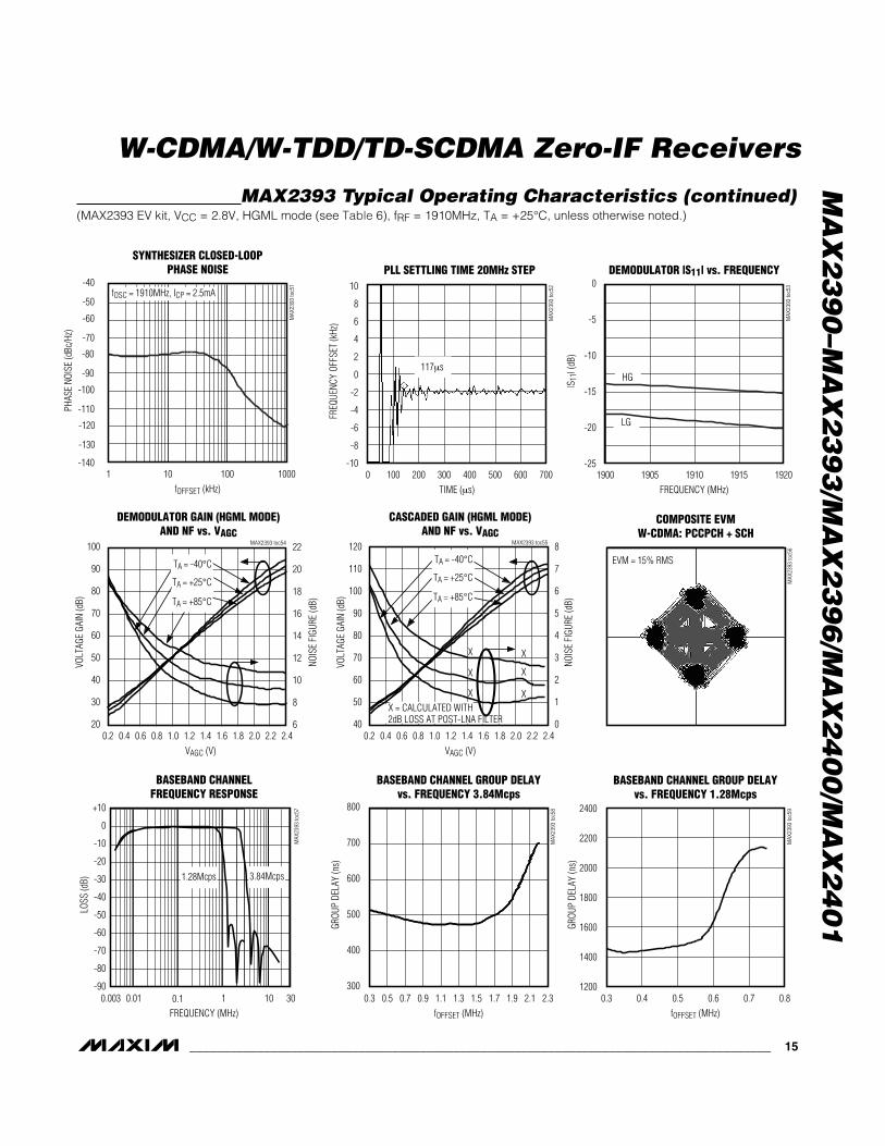
MAX2393 Typical Operating Characteristics(MAX2393 EV kit, VCC = 2.8V, HGML mode (see Table 6), fRF = 1910MHz, TA = +25°C, unless otherwise noted.)
MA
X2
39
0–M
AX
23
93
/MA
X2
39
6/M
AX
24
00
/MA
X2
40
1
W-CDMA/W-TDD/TD-SCDMA Zero-IF Receivers
______________________________________________________________________________________ 15
-50
-1401 100010010
SYNTHESIZER CLOSED-LOOPPHASE NOISE
-110
-130
-70
-90
-40
-100
-120
-60
-80
MAX
2393
toc5
1
fOFFSET (kHz)
PHAS
E NO
ISE
(dBc
/Hz)
fOSC = 1910MHz, ICP = 2.5mA
-10
-4
-6
-8
0
-2
8
6
4
2
10
0 100 200 300 400 500 600 700
MAX
2393
toc5
2
TIME (µs)
FREQ
UENC
Y OF
FSET
(kHz
)
PLL SETTLING TIME 20MHz STEP
117µs
DEMODULATOR |S11| vs. FREQUENCY
MAX
2393
toc5
3
FREQUENCY (MHz)
|S11
| (dB
)
-25
-20
-15
-10
-5
0
1900 1905 1910 1915 1920
HG
LG
20
30
90
50
40
60
70
80
100
0.2 0.6 0.8 1.00.4 1.2 1.4 2.01.8 2.21.6 2.4
DEMODULATOR GAIN (HGML MODE)AND NF vs. VAGC
MAX2393 toc54
VAGC (V)
VOLT
AGE
GAIN
(dB)
6
8
20
12
10
14
16
18
22
NOIS
E FI
GURE
(dB)
TA = +25°C
TA = -40°C
TA = +85°C
40
50
110
70
60
80
90
100
120
0.2 0.6 0.8 1.00.4 1.2 1.4 2.01.8 2.21.6 2.4
CASCADED GAIN (HGML MODE)AND NF vs. VAGC
MAX2393 toc55
VAGC (V)
VOLT
AGE
GAIN
(dB)
0
1
7
3
2
4
5
6
8
NOIS
E FI
GURE
(dB)
TA = +25°C
TA = -40°C
TA = +85°C
X = CALCULATED WITH2dB LOSS AT POST-LNA FILTER
X
X
X
X
X
X
EVM = 15% RMS
COMPOSITE EVMW-CDMA: PCCPCH + SCH
MAX
2393
toc5
6
+10
-900.003 30100.1 10.01
BASEBAND CHANNELFREQUENCY RESPONSE
MAX
2393
toc5
7
FREQUENCY (MHz)
LOSS
(dB)
-80
-70
-60
-50
-40
-30
-20
-10
0
1.28Mcps 3.84Mcps
500
400
300
600
700
800
0.3 0.7 0.9 1.10.5 1.3 1.5 1.7 2.11.9 2.3
BASEBAND CHANNEL GROUP DELAYvs. FREQUENCY 3.84Mcps
MAX
2393
toc5
8
fOFFSET (MHz)
GROU
P DE
LAY
(ns)
BASEBAND CHANNEL GROUP DELAYvs. FREQUENCY 1.28Mcps
MAX
2393
toc5
9
fOFFSET (MHz)
GROU
P DE
LAY
(ns)
0.70.60.50.4
1400
1600
1800
2000
2200
2400
12000.3 0.8
MAX2393 Typical Operating Characteristics (continued)(MAX2393 EV kit, VCC = 2.8V, HGML mode (see Table 6), fRF = 1910MHz, TA = +25°C, unless otherwise noted.)

MA
X2
39
0–M
AX
23
93
/MA
X2
39
6/M
AX
24
00
/MA
X2
40
1
W-CDMA/W-TDD/TD-SCDMA Zero-IF Receivers
16 ______________________________________________________________________________________
MAX2396 Typical Operating Characteristics(MAX2396 EV kit, VCC = 2.8V, HGML mode (see Table 6), fRF = 2140MHz, TA = +25°C, unless otherwise noted.)
0
5
10
15
20
25
30
35
40
2.7 2.92.8 3.0 3.1 3.2 3.3
HGHL MODESUPPLY CURRENT vs. SUPPLY VOLTAGE
MAX
2396
toc6
0
VCC (V)
I CC
(mA)
TA = -40°C TA = +25°C TA = +85°C
IDLE0
5
10
15
20
25
30
35
40
2.7 2.92.8 3.0 3.1 3.2 3.3
LG MODESUPPLY CURRENT vs. SUPPLY VOLTAGE
MAX
2396
toc6
1
VCC (V)
I CC
(mA)
TA = -40°C TA = +25°C TA = +85°C
IDLE-4
0
-2
4
2
8
6
10
2.7 2.9 3.02.8 3.1 3.2 3.3
LNA IN-BAND IIP3 vs. SUPPLY VOLTAGE
MAX
2396
toc6
2
VCC (V)
IIP3
(dBm
)
TA = -40°C
LG
HG
TA = +25°C TA = +85°C
LNA GAIN AND NF (HG MODE) vs. FREQUENCYMAX2396 toc63
FREQUENCY (MHz)
GAIN
(dB)
216021502120 2130 2140
11
12
13
14
15
16
17
18
10
NF (d
B)
0.5
1.0
1.5
2.0
2.5
3.0
3.5
4.0
02110 2170
TA = -40°C TA = +25°C TA = +85°C
VCO fOSC AND kVCO vs.VTUNE
VCC (V)
f OSC
(MHz
)
2.22.01.6 1.80.8 1.0 1.2 1.40.6
4000
4050
4100
4150
4200
4250
4300
4350
4400
4450
3950
125
150
175
200
225
250
275
300
325
350
1000.4 2.4
k VCO
(MHz
/V)
MAX2396 toc64
TA = -40°C TA = +25°C TA = +85°C
20
30
90
50
40
60
70
80
100
0.2 0.6 0.8 1.00.4 1.2 1.4 2.01.8 2.21.6 2.4
DEMODULATOR GAIN AND NF vs. VAGCMAX2396 toc65
VAGC (V)
VOLT
AGE
GAIN
(dB)
6
8
20
12
10
14
16
18
22
NOIS
E FI
GURE
(dB)
TA = +25°C
TA = -40°C
TA = +85°C
40
50
110
70
60
80
90
100
120
0.2 0.6 0.8 1.00.4 1.2 1.4 2.01.8 2.21.6 2.4
CASCADED GAIN AND NF vs. VAGCMAX2396 toc66
VAGC (V)
VOLT
AGE
GAIN
(dB)
0
1
7
3
2
4
5
6
8
NOIS
E FI
GURE
(dB)
TA = +25°C
TA = -40°C
TA = +85°C
= CALCULATED
WITH 2dB LOSS ATPOST-LNA FILTER
EVM = 15% RMS
COMPOSITE EVMW-CDMA: PCCPCH + SCH
MAX
2396
toc6
7 +10
-900.003 30100.1 10.01
FREQUENCY RESPONSEM
AX23
96 to
c68
FREQUENCY (MHz)
LOSS
(dB)
-80
-70
-60
-50
-40
-30
-20
-10
0

MA
X2
39
0–M
AX
23
93
/MA
X2
39
6/M
AX
24
00
/MA
X2
40
1
W-CDMA/W-TDD/TD-SCDMA Zero-IF Receivers
______________________________________________________________________________________ 17
SUPPLY CURRENT vs. SUPPLY VOLTAGEHGML MODE
MAX
2400
toc6
9
VCC (V)
I CC
(mA)
3.23.12.8 2.9 3.0
5
10
15
20
25
30
35
40
02.7 3.3
TA = -40°C TA = +25°C TA = +85°C
IDLE
SUPPLY CURRENT vs. SUPPLY VOLTAGELG MODE
MAX
2400
toc7
0
VCC (V)
I CC
(mA)
3.23.12.8 2.9 3.0
5
10
15
20
25
30
35
40
02.7 3.3
IDLE
TA = -40°C TA = +25°C TA = +85°C
LNA |S11| AND |S22| vs. FREQUENCY
MAX
2400
toc7
1
FREQUENCY (MHz)
|S11
|, |S
22| (
dB)
19801970196019501940
-15.0
-10.0
-5.0
0
-20.01930 1990
|S22|, LG|S11|, LG
|S22|, HG
|S11|, HG
LNA |S21| AND |S12| vs. FREQUENCY
MAX2400 toc72
FREQUENCY (MHz)
|S21
| (dB
)
|S12
| (dB
)
19801970196019501940
-5.0
0
5.0
10.0
15.0
20.0
-10.01930 1990
|S12|, HG
|S21|, LG
|S12|, LG
|S21|, HG
-38
-36
-34
-32
-30
-28
-26
-40
LNA IN-BAND IIP3vs. SUPPLY VOLTAGE
MAX
2400
toc7
3
VCC (V)
IIP3
(dBm
)
3.23.13.02.92.8
-4.0
-2.0
0
2.0
4.0
6.0
8.0
-6.02.7 3.3
LG
HG
TA = +85°C
TA = -40°C TA = +25°C
LNA GAIN AND NFvs. FREQUENCY HG MODE
MAX2400 toc74
FREQUENCY (MHz)
GAIN
(dB)
NF(d
B)
19801970196019501940
11
12
13
14
15
16
10
1.5
2.0
2.5
3.0
3.5
4.0
1.01930 1990
GAIN, -40°C
GAIN, +25°C
GAIN, +85°C
NF, +85°C
NF, +25°C
NF, -45°C
VCO fOSC AND kVCO vs. VTUNEMAX2400 toc75
VTUNE (V)
f OSC
(MHz
)
2.22.00.6 0.8 1.0 1.4 1.61.2 1.8
3750
3800
3850
3900
3950
4000
4050
4100
3700
k VCO
(MHz
/V)
125
150
175
200
225
250
275
300
1000.4 2.4
DEMODULATOR |S11| vs. FREQUENCY
MAX
2400
toc7
6
FREQUENCY (MHz)
|S11
| (dB
)
19801970196019501940
-18
-16
-14
-12
-10
-8
-6
-4
-2
0
-201930 1990
HGML
LG
MAX2400 Typical Operating Characteristics(MAX2400 EV kit, VCC = 2.8V, HGML mode (see Table 6), fRF = 1960MHz, TA = +25°C, unless otherwise noted.)

MA
X2
39
0–M
AX
23
93
/MA
X2
39
6/M
AX
24
00
/MA
X2
40
1
W-CDMA/W-TDD/TD-SCDMA Zero-IF Receivers
18 ______________________________________________________________________________________
DEMODULATOR GAIN AND NF vs. VAGCMAX2400 toc77
VAGC (V)
VOLT
AGE
GAIN
(dB)
NOIS
E FI
GURE
(dB)
2.22.01.6 1.80.6 0.8 1.0 1.2 1.40.4
10
0
20
30
40
50
60
70
80
90
20100
18
16
14
12
10
8
6
00.2 2.4
TA = -40°C
TA = +25°C
TA = +85°C
CASCADED GAIN AND NF vs. VAGCMAX2400 toc78
VAGC (V)
VOLT
AGE
GAIN
(dB)
NOIS
E FI
GURE
(dB)
2.22.01.6 1.80.6 0.8 1.0 1.2 1.40.4
30
20
40
50
60
70
80
90
100
110
120
1
0
2
3
4
5
6
7
8
9
10
0.2 2.4
TA = -40°C
TA = +25°C
TA = +85°C
CALCULATED1.4dB LOSS AT POST-LNA FILTER
EVM = 16.5% RMS
COMPOSITE EVMW-CDMA: PCCPCH + SCH
MAX
2400
toc7
9
BASEBAND CHANNELRESPONSE vs. FREQUENCY
MAX
2400
toc8
0
fOFFSET (MHz)
RESP
ONSE
, REL
ATIV
E TO
300
MHz
(dB)
1010.10.01
-80
-70
-60
-50
-40
-30
-20
-10
0
10
-900.001 100
BASEBAND CHANNELGROUP DELAY vs. FREQUENCY
MAX
2400
toc8
1
fOFFSET (MHz)
GROU
P DE
LAY
(ns)
2.11.90.5 0.7 0.9 1.3 1.51.1 1.7
500
600
700
800
900
1000
1100
1200
4000.3 2.3
MAX2400 Typical Operating Characteristics (continued)(MAX2400 EV kit, VCC = 2.8V, HGML mode (see Table 6), fRF = 1960MHz, TA = +25°C, unless otherwise noted.)

MA
X2
39
0–M
AX
23
93
/MA
X2
39
6/M
AX
24
00
/MA
X2
40
1
W-CDMA/W-TDD/TD-SCDMA Zero-IF Receivers
______________________________________________________________________________________ 19
0
5
10
15
20
25
30
35
40
2.7 2.92.8 3.0
TA = -40°C
3.1 3.2 3.3
HGML MODESUPPLY CURRENT vs. SUPPLY VOLTAGE
MAX
2401
toc8
2
VCC (V)
I CC
(mA) TA = +25°C
IDLE
TA = +85°C
0
5
10
15
20
25
30
35
40
2.7 2.92.8 3.0
TA = -40°C
3.1 3.2 3.3
LG MODESUPPLY CURRENT vs. SUPPLY VOLTAGE
MAX
2401
toc8
3
VCC (V)
I CC
(mA)
TA = +25°C
IDLE
TA = +85°C
-14
-13
-12
-11
-10
-9
1805 1820 1835 1850 1865 1880
MAX
2401
toc8
4
LNA |S11| AND |S22| vs. FREQUENCY
FREQUENCY (MHz)
|S11
|, |S
22| (
dB)
|S11|, HG
|S11|, LG
|S22|, LG |S22|, HG
-15
-5
-10
5
0
15
10
20
1805 1820 1835 1850 1865 1880
MAX2401 toc85
-44
-40
-42
-36
-38
-34LNA |S21| AND |S12| vs. FREQUENCY
FREQUENCY (MHz)
|S21
| (dB
)
|S12
| (dB
)
|S21|, HG
|S12|, LG
|S12|, HG
|S21|, LG-6
-2
-4
2
0
6
4
8
2.7 2.9 3.02.8 3.1 3.2 3.3
LNA IN-BAND IIP3 vs. SUPPLY VOLTAGE
MAX
2401
toc8
6
VCC (V)
IIP3
(dBm
)
TA = -40°C
LG
HG
TA = +25°C TA = +85°C
LNA GAIN AND NF vs. FREQUENCYMAX2401 toc87
FREQUENCY (MHz)
GAIN
(dB)
18651835 18501820
11
12
13
14
15
16
17
10
NF (d
B)
1.5
2.0
2.5
3.0
3.5
4.0
4.5
1.01805 1880
GAIN, TA = -40°C
NF, TA = +25°C
GAIN, TA = +85°C
NF, TA = -45°C
GAIN, TA = +25°C
NF, TA = +85°C
VCO fOSC AND kVCO vs. VTUNEMAX2401 toc88
VTUNE (V)
f OSC
(MHz
)
2.22.00.6 0.8 1.0 1.4 1.61.2 1.8
3600
3630
3660
3690
3720
3750
3780
3810
3570
k VCO
(MHz
/V)
70
90
110
130
150
170
190
210
500.4 2.4
MAX2401 Typical Operating Characteristics(MAX2401 EV kit, VCC = 2.8V, HGML mode (see Table 6), fRF = 1842.4MHz, TA = +25°C, unless otherwise noted.)

MA
X2
39
0–M
AX
23
93
/MA
X2
39
6/M
AX
24
00
/MA
X2
40
1
W-CDMA/W-TDD/TD-SCDMA Zero-IF Receivers
20 ______________________________________________________________________________________
MAX2401 Typical Operating Characteristics (continued)(MAX2401 EV kit, VCC = 2.8V, HGML mode (see Table 6), fRF = 1842.4MHz, TA = +25°C, unless otherwise noted.)
-1301 100010010
SYNTHESIZER CLOSED-LOOPPHASE NOISE
-100
-120
-80
-60
-90
-110
-70M
AX24
01 to
c89
fOFFSET (kHz)
PHAS
E NO
ISE
(dBc
/Hz)
fOSC = 1842.4MHz, ICP = 2.5mA
-10
-4
-6
-8
0
-2
8
6
4
2
10
0 100 200 300 400 500 600 700
MAX
2401
toc9
0
TIME (µs)
FREQ
UENC
Y OF
FSET
(kHz
)
PLL SETTLING TIME 60MHz STEP
203µs
DEMODULATOR |S11| vs. FREQUENCY
MAX
2401
toc9
1
FREQUENCY (MHz)
|S11
| (dB
)
-24
-21
-18
-15
-12
1805 1820 1835 1865 18801850
HGML
LG
30
90
50
40
60
70
80
100
0.2 0.6 0.8 1.00.4 1.2 1.4 2.01.8 2.21.6 2.4
DEMODULATOR GAIN AND NF vs. VAGCMAX2401 toc92
VAGC (V)
VOLT
AGE
GAIN
(dB)
7
9
13
11
15
17
19
21
NOIS
E FI
GURE
(dB)
TA = +25°C
TA = -40°C
TA = +85°C
40
50
110
70
60
80
90
100
120
0.2 0.6 0.8 1.00.4 1.2 1.4 2.01.8 2.21.6 2.4
CASCADED GAIN AND NF vs. VAGCMAX2401 toc93
VAGC (V)
VOLT
AGE
GAIN
(dB)
1
2
8
4
3
5
6
7
9
NOIS
E FI
GURE
(dB)
TA = +25°C
TA = -40°C
TA = +85°C
CALCULATEDWITH 1.4dB LOSSAT POST-LNAFILTER
EVM = 16% RMS
COMPOSITE EVMW-CDMA: PCCPCH + SCH
MAX
2401
toc9
4
BASEBAND CHANNELRESPONSE vs. FREQUENCY
MAX
2401
toc9
5
fOFFSET (MHz)
RESP
ONSE
, REL
ATIV
E TO
300
MHz
(dB)
1010.10.01
-80
-70
-60
-50
-40
-30
-20
-10
0
10
-900.001 100
BASEBAND CHANNELGROUP DELAY vs. FREQUENCY
MAX
2401
toc9
6
fOFFSET (MHz)
GROU
P DE
LAY
(ns)
2.11.90.5 0.7 0.9 1.3 1.51.1 1.7
500
600
700
800
900
1000
1100
1200
4000.3 2.3

MA
X2
39
0–M
AX
23
93
/MA
X2
39
6/M
AX
24
00
/MA
X2
40
1
W-CDMA/W-TDD/TD-SCDMA Zero-IF Receivers
______________________________________________________________________________________ 21
Pin Description
PIN NAME FUNCTION
1 VCC
Supply Pin for I/Q Mixers. This pin must be bypassed to system ground as close to the pin as possible.The ground vias for the bypass capacitor should not be shared by any other branch. Use 100pF for RFbypassing to GND.
2 RF+ N oni nver ti ng RF Inp ut to Z er o- IF D em od ul ator ( 200Ω D i ffer enti al N om i nal Im p ed ance Betw een RF+ and RF- )
3 RF- Inverting RF Input to Zero-IF Demodulator (200Ω Differential Nominal Impedance Between RF+ and RF-)
4 BIAS External Bias Resistor Connection
5 VCC
Supply Pin for LNA. This pin must be bypassed to system ground as close to the pin as possible.The ground vias for the bypass capacitor should not be shared by any other branch. Use 100pF for RFbypassing to GND.
6 G_LNA LNA Gain Mode Logic-Control Pin
7 LNA_OUT LNA Output. Internally matched to 50Ω.
8 GND RF Ground Return for LNA. Provide multiple vias to the system ground plane as close to the pin as possible.
9 LNA_IN LNA Input. Externally matched to 50Ω. See the Applications Information section for more information.
10 GNDRF VCO Varactor Ground Return. Provide multiple vias to the system ground plane as close to the pinas possible.
11 VCC
Supply Pin for VCO. This pin must be bypassed to system ground as close to the pin as possible.The ground vias for the bypass capacitor should not be shared by any other branch. Use 100pF for RFbypassing to GND.
12 TUNE RF VCO Varactor TUNE Input. Connect PLL loop filter between CP and TUNE.
CP(MAX2390–MAX2393, MAX2401) High-Impedance Output of the RF Charge Pump. The RF PLL’s loop filter isconnected between this pin and TUNE.13
LO_OUT+ (MAX2396/MAX2400) VCO Divide-by-3 Noninverting Output to Synthesizer
VCC (MAX2390–MAX2393, MAX2401) Supply Pin for Synthesizer Charge Pump. Use 100nF for bypassing to GND.14
LO_OUT- (MAX2396/MAX2400) VCO Divide-by-3 Inverting Output to Synthesizer
15 VCC Supply Pin for On-Chip Digital Circuitry. Use 100nF for bypassing to GND.
16 REFIN Synthesizer Reference Frequency Input. AC-couple to the reference source through 1nF.
LD(MAX2390–MAX2393, MAX2401) Open-Drain Output Indicating LOCK Status of the RF PLL. It is open drain towire-OR with LD from TX chip.
17IDLE
(MAX2396/MAX2400) Idle Mode Enable. Drive IDLE low to disable all blocks except serial bus, VCO, anddivide-by-3 prescaler to PLL.
18 SHDN Shutdown Logic Pin for Entire Receiver (Active Low)
19 AGC Analog Input Pin Controlling the Baseband VGA Gain
20 Q+ Noninverting Baseband Output for Q Channel
21 Q- Inverting Baseband Output for Q Channel
22 I- Inverting Baseband Output for I Channel
23 I+ Noninverting Baseband Output for I Channel
24 VCC Supply Pin for Baseband Circuitry. Use 100nF for bypassing to GND.
25 CS 3-Wire Serial Bus Enable Input (Active Low)
26 G_MXR Mixer Gain Mode Logic-Control Pin
27 SDATA 3-Wire Serial Bus Data Input
28 SCLK 3-Wire Serial Bus Clock Input

MA
X2
39
0–M
AX
23
93
/MA
X2
39
6/M
AX
24
00
/MA
X2
40
1
W-CDMA/W-TDD/TD-SCDMA Zero-IF Receivers
22 ______________________________________________________________________________________
28 27 26
21
20
19
1
2
3
184
17
16
5
6
157
25 24 23 22
8 9 10 11 12 13 14
Q-
Q+
AGC
SHDN
IDLE
REFIN
VCC
LO_O
UT-
VCC
RF+
RF-
BIAS
VCC
G_LNA
LNA_OUT TANK
SCLK
SDAT
A
G_M
XR
I+ I-CS V CC
GND
LNA_
IN
GND
LO_O
UT+
V CC
TUNE
MAX2396MAX2400
/3
SERIALINTERFACE
/2
LNA
Pin Configuration/Functional Diagram for MAX2396/MAX2400

MA
X2
39
0–M
AX
23
93
/MA
X2
39
6/M
AX
24
00
/MA
X2
40
1
W-CDMA/W-TDD/TD-SCDMA Zero-IF Receivers
______________________________________________________________________________________ 23
W-CDMA FDD Receiver Operating Circuit (MAX2390/MAX2391/MAX2401)
28 27 26
21
DACMAX5383 (6-PIN SOT)
(OPTIONAL EXTERNAL AGC DAC,USES 3-WIRE INTERFACE)
20
19
1
2
3
184
17
16
5
6
157
25 24 23 22
8 9 10 11 12 13 14
Q-
Q+
AGC
SHDN
LD
REFIN
TCXO19.2MHz (MAX2390/MAX2391)
26MHz (MAX2401)BA
SEBA
ND/D
SP
VCC
VCC
RF+
RF-
+2.8V
+2.8V
BIAS
VCC
G_LNA
LNA_OUT
Tx (FROM PA)
TANK
SCLK
SDAT
A
G_M
XR
I+
I-CS V CC
GND
LNA_
IN
GND CP V CC
V CC
TUNE
MAX2390/MAX2391MAX2401
INTEGER-NPLL
SERIALINTERFACE
/2
LNARx
+2.8V +2.8V
+2.8V
+2.8V
DAC CS
MA
X2
39
0–M
AX
23
93
/MA
X2
39
6/M
AX
24
00
/MA
X2
40
1
W-CDMA/W-TDD/TD-SCDMA Zero-IF Receivers
24 ______________________________________________________________________________________
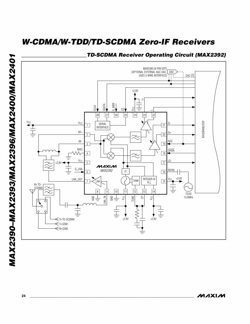
TD-SCDMA Receiver Operating Circuit (MAX2392)
28 27 26
21
DACMAX5383 (6-PIN SOT)
(OPTIONAL EXTERNAL AGC DAC,USES 3-WIRE INTERFACE)
20
19
1
2
3
184
17
16
5
6
157
25 24 23 22
8 9 10 11 12 13 14
Q-
Q+
AGC
SHDN
LD
REFIN
BASE
BAND
/DSP
VCC
VCCVCC
RF+
RF-
+2.8V
BIAS
VCC
G_LNA
LNA_OUT TANK
SCLK
SDAT
A
G_M
XR
I+
I-CS V CC
GND
LNA_
IN
GND CP V CC
V CC
TUNE
MAX2392
INTEGER-NPLL
SERIALINTERFACE
/2
LNARx TD-SCDMA
+2.8V +2.8V
+2.8V
+2.8V
DAC CS
Tx TD-SCDMA
Tx GSM
Rx GSM
TCXO13.0MHz

MA
X2
39
0–M
AX
23
93
/MA
X2
39
6/M
AX
24
00
/MA
X2
40
1
W-CDMA/W-TDD/TD-SCDMA Zero-IF Receivers
______________________________________________________________________________________ 25
W-TDD Receiver Operating Circuit (MAX2393)
28 27 26
21
DACMAX5383 (6-PIN SOT)
(OPTIONAL EXTERNAL AGC DAC,USES 3-WIRE INTERFACE)
20
19
1
2
3
184
17
16
5
6
157
25 24 23 22
8 9 10 11 12 13 14
Q-
Q+
AGC
SHDN
LD
REFIN
BASE
BAND
/DSP
VCC
VCCVCC
RF+
RF-
+2.8V
BIAS
VCC
G_LNA
LNA_OUT TANK
SCLK
SDAT
A
G_M
XR
I+
I-CS V CC
GND
LNA_
IN
GND CP V CC
V CC
TUNE
MAX2393
INTEGER-NPLL
SERIALINTERFACE
/2
LNARx TDD
+2.8V +2.8V
+2.8V
+2.8V
DAC CS
Tx TDD
TCXO19.2MHz

MA
X2
39
0–M
AX
23
93
/MA
X2
39
6/M
AX
24
00
/MA
X2
40
1
W-CDMA/W-TDD/TD-SCDMA Zero-IF Receivers
26 ______________________________________________________________________________________
W-CDMA FDD Receiver Operating Circuit (External Synthesizer)(MAX2396/MAX2400)
28 27 26
21
DACMAX5383 (6-PIN SOT)
(OPTIONAL EXTERNAL AGC DAC,USES 3-WIRE INTERFACE)
20
19
1
2
3
184
17
16
5
6
157
25 24 23 22
8 9 10 11 12 13 14
Q-
Q+
AGC
SHDN
IDLE
REFIN
TCXO15.36MHz
BASE
BAND
/DSP
VCC
VCC
RF+
RF-
+2.8V
+2.8V
BIAS
VCC
G_LNA
LNA_OUT
Tx (FROM PA)
TANK
SCLK
SDAT
A
G_M
XR
I+
I-CS V CC
GND
LNA_
IN
GND
LO_O
UT+
LO_O
UT-
V CC
TUNE
MAX2396MAX2400
/3
SERIALINTERFACE
/2
LNARx
+2.8V
FROMEXTERNAL
PLL
TO EXTERNAL PLL
+2.8V
+2.8V

MA
X2
39
0–M
AX
23
93
/MA
X2
39
6/M
AX
24
00
/MA
X2
40
1
W-CDMA/W-TDD/TD-SCDMA Zero-IF Receivers
______________________________________________________________________________________ 27
Detailed DescriptionWith the exception of the analog-input AGC, all func-tionality of these direct-conversion receivers can becontrolled through the 3-wire serial interface(SPI™/QSPI™/MICROWIRE™ compatible).
Register DefinitionAll devices in this family have two programmable 20-bitregisters: the configuration register (CONFIG) and thecontrol register (OPCNTRL). The MAX2391/MAX2392/MAX2393/MAX2401 have two additional programmable20-bit registers: the main PLL divide register (RFM) andthe reference PLL divide register (RFR). The 4 least sig-nificant bits of the data sent are the register’s address.The 16 most significant bits are used for register data.All registers contain a few don’t care bits. These can beeither 0 or 1 and do not affect operation. Tables 1a and1b provide a register summary. Data is shifted in MSBfirst. When CS is low, data is shifted with the risingedge of the clock. When CS transitions to high, the shiftregister is latched into the register selected by the con-tents of the address bits. Power-up defaults for the fourregisters are shown in Table 2.
The RFM register sets the main-frequency divide ratiofor the RF PLL. The RFR register sets the reference-fre-quency divide ratio. The RF LO frequency can bedetermined by the following:
RF LO frequency = fREFIN x (RFM / RFR)
where fREFIN is the external input reference frequency
for the MAX2390–MAX2393, MAX2401.
The operation control register (OPCNTRL) and the con-figuration register (CONFIG) are used to program thereceiver for the appropriate mode of operation. SeeTables 3 and 4 for the function of each bit.
The test register is used to set the receiver in factorytesting mode. It should only be programmed at receiverturn-on with the word 0370 (hex) for MAX2390–MAX2393,MAX2401 and 2370 (hex) for MAX2396/MAX2400.
Power ManagementBias control is distributed among several functional sec-tions and can be controlled to accommodate differentpower-down modes as shown in Table 5.
The IC has three bias states: SHUTDOWN, IDLE, andON. SHUTDOWN can be asserted by either a hardwarecontrol line (SHDN) or by bit 5 of the operation controlregister (OPCTRL.SHDN). When the serial interface isused to shut down the part, an internal linear regulator,with IQ ≈ 90µA, stays functional to keep the serial inter-face operational. Use the SHDN logic-control pin tobring quiescent current below 10µA. Register bit set-tings maintain their values after a hard shutdown, pro-vided CS remains high. IDLE mode disables the LNA,I/Q mixers, and baseband circuitry, but keeps the serialinterface and synthesizer operational, dropping quies-cent current to 11.5mA. The entire receiver is ON whenSHDN is high and OPCNTRL.SHDN andOPCNTRL.IDLE bits (MAX2390–MAX2393, MAX2401)or the IDLE pin (MAX2396/MAX2400) are set to 1; thetypical supply current is 32mA.
Table 1a. Register Defintion (MAX2390–MAX2393, MAX2401)MSB 20-BIT REGISTER LSB
DATA 16 BITS ADDRESS 4 BITSREGISTER
NAMEB15 B14 B13 B12 B11 B10 B9 B8 B7 B6 B5 B4 B3 B2 B1 B0 A3 A2 A1 A0
RFM X
M14
M13
M12
M11
M10 M9
M8
M7
M6
M5
M4
M3
M2
M1
M0 0 0 1 1
RFR X X X X X X X R8
R7
R6
R5
R4
R3
R2
R1
R0 0 1 1 1
OPCNTRL X X X X
(RE
SE
RV
ED
)
(RE
SE
RV
ED
)
(RE
SE
RV
ED
)
(RE
SE
RV
ED
)
RC
1
RC
0
SHDN
IDLE
GLN
A
LMX
R
GM
XR
VC
M
1 0 1 1
CONFIG X X X X
(RE
SE
RV
ED
)
(RE
SE
RV
ED
)
(RE
SE
RV
ED
)
(RE
SE
RV
ED
)
(RE
SE
RV
ED
)
BW
_SE
L
DC
_CA
NC
EL_
EN
RF_
PLL
_EN
VC
O_E
N
CP
1
CP
0
LNA
_EN
1 1 1 1
MICROWIRE is a trademark of National Semiconductor Corp. SPI and QSPI are trademarks of Motorola, Inc.

MA
X2
39
0–M
AX
23
93
/MA
X2
39
6/M
AX
24
00
/MA
X2
40
1
W-CDMA/W-TDD/TD-SCDMA Zero-IF Receivers
28 ______________________________________________________________________________________
Table 1b. Register Defintion (MAX2396/MAX2400)
MSB 20-BIT REGISTER LSB
DATA 16 BITS ADDRESS 4 BITSREGISTER
NAMEB15 B14 B13 B12 B11 B10 B9 B8 B7 B6 B5 B4 B3 B2 B1 B0 A3 A2 A1 A0
OPCNTRL X X X X
(RE
SE
RV
ED
)
(RE
SE
RV
ED
)
(RE
SE
RV
ED
)
(RE
SE
RV
ED
)
RC
1
RC
0
SHDN
(RE
SE
RV
ED
)
GLN
A
LMX
R
GM
XR
VC
M
1 0 1 1
CONFIG X X X X
(RE
SE
RV
ED
)
(RE
SE
RV
ED
)
(RE
SE
RV
ED
)
(RE
SE
RV
ED
)
(RE
SE
RV
ED
)
(RE
SE
RV
ED
)
DC
_CA
NC
EL_
EN
LO_G
EN
_EN
VC
O_E
N
(RE
SE
RV
ED
)
(RE
SE
RV
ED
)
LNA
_EN
1 1 1 1
Data shifted in MSB first.X represents a “don’t care.”Set all (RESERVED) bits to 0.
Table 2. Power-Up Default Register Settings
REGISTER ADDRESS DEFAULT FUNCTION
0x29CC (107800DEC)* MAX2391
0x2768 (10088DEC)* MAX2392
0x254E (9550DEC)* MAX2393RFM 0011b
0x2648 (9800DEC)* MAX2390, MAX2401
RF Main-DividerCount
0x0060 (0096DEC)* MAX2390/MAX2391/MAX2393/MAX2401RFR 0111b
0x0041 (0065DEC)* MAX2392RF Reference-Divider Count
OPCTRL 1011b 03B hex Operation control settings
CONFIG 1111b 07F hex Configuration control settings
0370 hex** MAX2390–MAX2393, MAX2401TEST 0001b
2370 hex** MAX2396/MAX2400Disables TestMode
Data shifted in MSB first.X represents a “don’t care.”Set all (RESERVED) bits to 0.*200kHz comparison frequency.**Needs to be programmed at receiver turn-on.

MA
X2
39
0–M
AX
23
93
/MA
X2
39
6/M
AX
24
00
/MA
X2
40
1
W-CDMA/W-TDD/TD-SCDMA Zero-IF Receivers
______________________________________________________________________________________ 29
Table 3. Operation Control Register (OPCNTRL, Address 1011)
BIT(B0 = LSB)
POWER-UPSTATE
BIT NAME FUNCTION
B11, B10, B9, B8 0 0 0 0 (RESERVED) Set to zero for normal operation.
B7, B6 0 0 RC1, RC0
Sets the -3dB corner of the highpass filter used for DC offset removal atbaseband (only possible when the automatic DC-offset-cancellation bit(CONFIG.B5) is disabled):0 0 = 8.6kHz highpass corner0 1 = 17.2kHz highpass corner1 0 = 100kHz highpass corner1 1 = 1MHz highpass corner
B5 1 SHDNZero shuts down everything except serial interface and registers, retainingtheir values.
IDLEFor M AX 2390–M AX 2393/M AX 2401:Z er o shuts d ow n ever ythi ng excep t RF P LL, RF V C O , ser i al i nter face, and r eg i ster s, r etai ni ng thei r val ues.B4 1
(RESERVED)For M AX 2396/M AX 2400:S et to 1 for nor m al op er ati on.
B3 1 GLNASets LNA operating mode according to the following:1 = high gain0 = low gain
B2 0 LMXRSets mixer linearity in high-gain mode:0 = medium linearity1 = high linearity
B1 1 GMXRSets MIXER operating mode according to the following:1 = high gain0 = low gain
B0 1 VCMSets output common-mode voltage for baseband I/Q outputs:0 = 1.2V1 = 1.42V

MA
X2
39
0–M
AX
23
93
/MA
X2
39
6/M
AX
24
00
/MA
X2
40
1
W-CDMA/W-TDD/TD-SCDMA Zero-IF Receivers
30 ______________________________________________________________________________________
Table 4. Configuration Register (CONFIG, Address 1111)
BITPOWER-UP
STATEBIT NAME FUNCTION
B11, B10, B9,B8, B7
0 0 0 0 0 (RESERVED) Set to 0 for normal operation.
BW_SELFor MAX2393 only:1 = selects the 3G W-CDMA mode for baseband filters.0 = selects the TD-SCDMA mode for baseband filters.B6 1
(RESERVED) Set to 1 for normal operation.
B5 1 DC_CANCEL_EN 0 = disables the automatic DC-offset-cancellation circuit.
RF_PLL_ENFor MAX2390–MAX2393/MAX2401:0 = disables the RF PLL + LO generation circuit.
B4 1
LO_GEN_ENFor MAX2396/MAX2400:0 = disables the LO generation circuit.
B3 1 VCO_EN 0 = disables the VCO.
CP1, CP0
For MAX2390–MAX2393/MAX2401:A 2-bit word sets the RF charge-pump current as follows:0 0 = 1000µA0 1 = 1500µA1 0 = 2000µA1 1 = 2500µA
B2, B1 1 1
(RESERVED)For MAX2396/MAX2400:Set to 11 for normal operation.
B0 1 LNA_EN 0 = disables on-chip LNA. Set to zero for external LNA.

MA
X2
39
0–M
AX
23
93
/MA
X2
39
6/M
AX
24
00
/MA
X2
40
1
W-CDMA/W-TDD/TD-SCDMA Zero-IF Receivers
______________________________________________________________________________________ 31
Table 5. Power-Down Modes
LOGIC
POWER-DOWNMODES
COMMENTS
SHDN
PIN
SHDN
BIT
IDLE
BIT
SE
RIA
L IN
TE
RF
AC
E
LN
A +
I/Q
MIX
ER
S +
BB
CIR
CU
ITR
Y
RF
VC
O +
RF
PL
L +
LO
GE
NE
RA
TIO
N
SHDN pin is HIGH, SHDN bit is ZERO.All blocks are OFF except serial bus and registers, whichretain their values; a LOW on SHDN pin overrides SHDN bit.
1 0 ON
SHUTDOWN
SHDN pin is LOW.All blocks are OFF; registers retain their preshutdown values.
0 X
X
OFF
OFF OFF
IDLEIDLE bit (OPCTRL.B4) is ZERO.All blocks are OFF except RF PLL, RF VCO, serial bus, andregisters, which retain their values.
1 1 0 ON OFF ON
Table 6. Operational Modes
EXTERNAL CONTROL PINS/OPCTRL REGISTER BITS
MIXER LNA
GMXR GLNA
MODE*
LMXR(BIT) (PIN) (BIT) (PIN) (BIT)
CORRESPONDING LNAMODE
CORRESPONDING MIXERMODE
HGML 0 1 1 1 1 High gain High gain, medium linearity
HGHL 1 1 1 1 1 High gain High gain, high linearity
1 0MG X
0 X1 1 High gain Low gain
1 0 1 0LG X
0 X 0 XLow gain Low gain
*Definitions:HGML: high gain, medium linearityHGHL: high gain, high linearityMG: medium gainLG: low gain

MA
X2
39
0–M
AX
23
93
/MA
X2
39
6/M
AX
24
00
/MA
X2
40
1
W-CDMA/W-TDD/TD-SCDMA Zero-IF Receivers
32 ______________________________________________________________________________________
Applications InformationLNA and RFIN Matching
The LNA requires a simple two-element 50Ω matchingnetwork at the input. Use the layout and matching net-work provided in the EV kit as a reference. The LNA inputis internally biased, so be sure to use a series 100pF DCblocking capacitor in front of the matching network.
The LNA offers a 23dB gain step with less than 10degrees phase change, selectable with either a dedi-cated logic pin (G_LNA) or bit 3 in the operation controlregister (OPCTRL.GLNA).
LNA output matching is provided on-chip, offering bet-ter than 2:1 VSWR. The required DC blocking capacitoris provided on-chip, so the LNA output can be connect-ed directly to the RF SAW filter or balun.
I/Q MixersThe mixers’ differential input impedance is 200Ω, allow-ing an easy interface to commercially available differ-ential-output Rx SAW filters or 1:4 baluns. No DCblocks are required, but a single, small shunt inductoris required to resonate out the parasitic capacitancefrom the SAW filter and IC package.
The mixer offers an 11dB gain step, which is controlledby either the logic-control pin (G_MXR) or bit 1 of theoperation control register (OPCTRL.GMXR). This offersthe option to switch the mixer into a low-gain state ifrequired, reducing current consumption by about 3mA.Use the mixer gain step and AGC before reducing LNAgain for optimum receiver dynamic range.
Baseband I/Q FiltersAll receiver channel selectivity is implemented fully on-chip, with greater than 40dB adjacent channel selectivi-ty (ACS). This eliminates the need for any additionalfiltering by any subsequent baseband processor.
The group delay of the integrated filters is compensat-ed through on-chip equalizers for optimum EVM.
AGCThe AGC circuitry of the baseband amplifiers offers lin-ear (dB/V) gain control for the receiver. With the AGCvoltage from 0.3V to 2.4V, the VGA section provides60dB gain-control range, for a total of 95dB includingthe LNA and mixer gain steps.
The AGC control line has an input impedance of morethan 100kΩ at DC. Internal capacitance creates a single
pole at approximately 2MHz; this provides some high-frequency filtering, thereby reducing AM distortion.
For applications using a baseband processor with digi-tal-only AGC, Maxim offers an 8-bit voltage-output AGCDAC with an SPI/QSPI/MICROWIRE interface in a tiny6-pin SOT23 package. Especially designed as a low-cost, all-in-one solution for cellular handset AGC, theMAX5383 offers the following features: a serial interfacegood to 10MHz, guaranteed operation from a 2.7V to3.6V supply, on-chip 2V reference, <±10% full-scaleerror, <±1LSB INL/DNL, <1µA shutdown, and a minis-cule 150µA supply current. See the Typical ApplicationCircuits for example application circuits using an exter-nal AGC DAC.
DC Offset CorrectionFor optimum IP2 and lowest DC offset at the basebandoutputs, a 3-pole Butterworth highpass filter is imple-mented on-chip. In normal operation, this highpass cor-ner is set to 8.6kHz. The corner frequency is chosen tooptimize DC settling time when the system is faced withlarge DC transients due to an LNA gain step or a largeAGC change between receive bursts.
An additional adaptive DC-cancellation mode has beenimplemented, which is activated for any of the followingevents: IC is enabled with IDLE, IC is enabled withSHDN, an LNA gain step (through logic pin or registersetting), or a mixer gain step (through logic pin or reg-ister setting). This adaptive DC correction loop furtherminimizes DC settling time for cases where large DCerrors are introduced. For further flexibility, the SPIinterface can be used to sequence the DC cancellationloop through different time constants (see Table 3).
Baseband I/Q InterfaceThe baseband I and Q differential outputs are designedfor a 150mVRMS W-CDMA combined signal plus noise.The 8dB peak-to-average ratio of the forward W-CDMAchannel brings the typical voltage at the baseband out-puts to 1.0VP-P. The baseband amplifiers’ outputs areDC-coupled, and offer a programmable common-modevoltage to address the requirements of different base-band processors’ ADCs. The output common-mode volt-age is 1.2V with OPCTRL VCM = 0, and 1.4V for VCM = 1(see Table 2 for the OPCTRL register definitions).
These outputs are designed for a minimum load of10kΩ (differential) in parallel with 5pF.

MA
X2
39
0–M
AX
23
93
/MA
X2
39
6/M
AX
24
00
/MA
X2
40
1
W-CDMA/W-TDD/TD-SCDMA Zero-IF Receivers
Maxim cannot assume responsibility for use of any circuitry other than circuitry entirely embodied in a Maxim product. No circuit patent licenses areimplied. Maxim reserves the right to change the circuitry and specifications without notice at any time.
Maxim Integrated Products, 120 San Gabriel Drive, Sunnyvale, CA 94086 408-737-7600 ____________________ 33
© 2005 Maxim Integrated Products Printed USA is a registered trademark of Maxim Integrated Products, Inc.
Synthesizer and LO GenerationThe MAX2390–MAX2393, MAX2401 incorporate an inte-ger-N synthesizer on-chip, including the VCO, tank, alldividers, phase comparator, etc. Only a TCXO and aloop filter are required as external components. The LOleakage at the LNA input is minimized by running theinternal VCO at 2x the desired LO frequency. The typicalapplication uses a comparison frequency of 200kHz—the channel raster for 3GPP-FDD and -TDD systems.
There are no special requirements for the synthesizerloop filter. The EV kits use a classic Type-II loop filter,with a bandwidth of about 20kHz. This ensures a 200µssettling time for a 60MHz frequency jump.
Use a 1nF DC-blocking capacitor in series with the ref-erence oscillator input so as not to disturb the DC bias.
The MAX2396/MAX2400 integrate the VCO and thedivide-by-2 for the LO generation, but do not includethe synthesizer. The LO leakage at the LNA input isminimized by running the VCO at twice the desired RFfrequency. The VCO signal is made available to theexternal PLL through an on-chip divide-by-threeprescaler. Since fVCO_OUTPUT = fVCO / 3, and fRFLO =fVCO / 2, then fVCO_OUTPUT = (2/3)fRFLO. That is, whenthe RFLO of the MAX2400 is running at midband(1960MHz), the VCO output and the synthesizer arerunning at 1306.67MHz.
Package InformationFor the latest package outline information, go towww.maxim-ic.com/packages.