w5500 datasheet - sparkfun electronics · spi (serial peripheral interface) ... 2.3 variable length...
TRANSCRIPT

© Copyright 2013 WIZnet Co., Ltd. All rights reserved.
W5500 Datasheet Version 1.0.2
http://www.wiznet.co.kr

2 / 66 W5500 Datasheet Version1.0.2 (November 2013)
W5500
The W5500 chip is a Hardwired TCP/IP embedded Ethernet controller that provides
easier Internet connection to embedded systems. W5500 enables users to have the
Internet connectivity in their applications just by using the single chip in which
TCP/IP stack, 10/100 Ethernet MAC and PHY embedded.
WIZnet‘s Hardwired TCP/IP is the market-proven technology that supports TCP, UDP,
IPv4, ICMP, ARP, IGMP, and PPPoE protocols. W5500 embeds the 32Kbyte internal
memory buffer for the Ethernet packet processing. If you use W5500, you can
implement the Ethernet application just by adding the simple socket program. It’s
faster and easier way rather than using any other Embedded Ethernet solution. Users
can use 8 independent hardware sockets simultaneously.
SPI (Serial Peripheral Interface) is provided for easy integration with the external
MCU. The W5500’s SPI supports 80 MHz speed and new efficient SPI protocol for the
high speed network communication. In order to reduce power consumption of the
system, W5500 provides WOL (Wake on LAN) and power down mode.
Features
- Supports Hardwired TCP/IP Protocols : TCP, UDP, ICMP, IPv4, ARP, IGMP, PPPoE
- Supports 8 independent sockets simultaneously
- Supports Power down mode
- Supports Wake on LAN over UDP
- Supports High Speed Serial Peripheral Interface(SPI MODE 0, 3)
- Internal 32Kbytes Memory for TX/RX Buffers
- 10BaseT/100BaseTX Ethernet PHY embedded
- Supports Auto Negotiation (Full and half duplex, 10 and 100-based )
- Not supports IP Fragmentation
- 3.3V operation with 5V I/O signal tolerance
- LED outputs (Full/Half duplex, Link, Speed, Active)
- 48 Pin LQFP Lead-Free Package (7x7mm, 0.5mm pitch)

W5500 Datasheet Version1.0.2 (November 2013) 3 / 66
Target Applications
W5500 is suitable for the following embedded applications:
- Home Network Devices: Set-Top Boxes, PVRs, Digital Media Adapters
- Serial-to-Ethernet: Access Controls, LED displays, Wireless AP relays, etc.
- Parallel-to-Ethernet: POS / Mini Printers, Copiers
- USB-to-Ethernet: Storage Devices, Network Printers
- GPIO-to-Ethernet: Home Network Sensors
- Security Systems: DVRs, Network Cameras, Kiosks
- Factory and Building Automations
- Medical Monitoring Equipment
- Embedded Servers
4 / 66 W5500 Datasheet Version1.0.2 (November 2013)
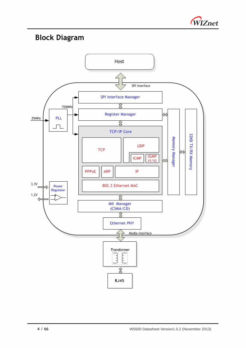
Block Diagram

W5500 Datasheet Version1.0.2 (November 2013) 5 / 66
Table of Contents
Pin Assignment .......................................................................................... 7 1
1.1 Pin Descriptions .............................................................................. 7
HOST Interface ......................................................................................... 12 2
2.1 SPI Operation Mode ........................................................................ 13
2.2 SPI Frame .................................................................................... 14
2.2.1 Address Phase......................................................................... 14
2.2.2 Control Phase ......................................................................... 15
2.2.3 Data Phase ............................................................................ 17
2.3 Variable Length Data Mode (VDM) ....................................................... 17
2.3.1 Write Access in VDM ................................................................. 18
2.3.2 Read Access in VDM .................................................................. 21
2.4 Fixed Length Data Mode (FDM) .......................................................... 24
2.4.1 Write Access in FDM ................................................................. 25
2.4.2 Read Access in FDM .................................................................. 26
Register and Memory Organization ................................................................ 27 3
3.1 Common Register Block ................................................................... 29
3.2 Socket Register Block ...................................................................... 30
3.3 Memory ...................................................................................... 31
Register Descriptions ................................................................................. 32 4
4.1 Common Registers ......................................................................... 32
4.2 Socket Registers ............................................................................ 44
Electrical Specifications ............................................................................. 59 5
5.1 Absolute Maximum Ratings ............................................................... 59
5.2 Absolute Maximum Ratings (Electrical Sensitivity) ................................... 59
5.3 DC Characteristics ......................................................................... 60
5.4 POWER DISSIPATION ........................................................................ 61
5.5 AC Characteristics ......................................................................... 61
5.5.1 Reset Timing .......................................................................... 61
5.5.2 Wake up Time ......................................................................... 61
5.5.3 Crystal Characteristics .............................................................. 61
5.5.4 SPI Timing ............................................................................. 62
5.5.5 Transformer Characteristics ........................................................ 63
5.5.6 MDIX .................................................................................... 63
Package Descriptions ................................................................................. 64 6
Document History Information ......................................................................... 65
6 / 66 W5500 Datasheet Version1.0.2 (November 2013)
Table of Figures
Figure 1. W5500 Pin Layout ....................................................................... 7
Figure 2. External reference resistor ......................................................... 11
Figure 3. Crystal reference schematic ........................................................ 11
Figure 4. Variable Length Data Mode (SCSn controlled by the host) .................... 12
Figure 5. Fixed Length Data Mode (SCSn is always connected by Ground) ............. 12
Figure 6. SPI Mode 0 & 3 ........................................................................ 13
Figure 7. SPI Frame Format ..................................................................... 14
Figure 8. Write SPI Frame in VDM mode ...................................................... 18
Figure 9. SIMR Register Write in VDM Mode .................................................. 19
Figure 10. 5 Byte Data Write at 1th Socket’s TX Buffer Block 0x0040 in VDM mode .. 20
Figure 11. Read SPI Frame in VDM mode ..................................................... 21
Figure 12. S7_SR Read in VDM Mode ........................................................... 22
Figure 13. 5 Byte Data Read at Socket 3 RX Buffer Block 0x0100 in VDM mode ....... 23
Figure 14. 1 Byte Data Write SPI Frame in FDM mode...................................... 25
Figure 15. 2 Bytes Data Write SPI Frame in FDM mode .................................... 25
Figure 16. 4 Bytes Data Write SPI Frame in FDM mode .................................... 25
Figure 17. 1 Byte Data Read SPI Frame in FDM mode ...................................... 26
Figure 18. 2 Bytes Data Read SPI Frame in FDM mode ..................................... 26
Figure 19. 4 Bytes Data Read SPI Frame in FDM mode ..................................... 26
Figure 20. Register & Memory Organization ................................................. 28
Figure 21. INTLEVEL Timing ..................................................................... 34
Figure 22. Reset Timing .......................................................................... 61
Figure 23. SPI Timing ............................................................................. 62
Figure 24. Transformer Type .................................................................... 63
Figure 25. Package Dimensions ................................................................. 64

W5500 Datasheet Version1.0.2 (November 2013) 7 / 66
Pin Assignment 1
Figure 1. W5500 Pin Layout
1.1 Pin Descriptions
Table 1. Pin Type Notation
Type Description
I Input
O Output
I/O Input / Output
A Analog
PWR 3.3V power
GND Ground
TXN
TXP
AGND
AVDD
RXN
RXP
DNC
AVDD
AGND
EXRES1
AVDD
NC
1
2
3
4
5
6
7
8
9
10
11
12
36
35
34
33
32
31
30
29
28
27
26
25
W5500
NC
AG
ND
AVD
D
AG
ND
AVD
D
VBG
AG
ND
TO
CAP
AVD
D
1V2O
RSVD
SPD
LED
MOSI
MISO
SCLK
SCSn
XO
XI/CLKIN
GND
VDD
ACTLED
DUPLED
LINKLED
INTn
AG
ND
NC
NC
PM
OD
E0
PM
OD
E1
PM
OD
E2
RSVD
RSVD
RSVD
RSVD
RSVD
RSTn
13
14
15
16
17
18
19 20
21
22
23
24
48
47
46
45
44
43
42
41
40
39
38
37
48LQFP
8 / 66 W5500 Datasheet Version1.0.2 (November 2013)
Table 2. W5500 Pin Description
Pin No Symbol Internal
Bias1 Type Description
1 TXN - AO TXP/TXN Signal Pair
The differential data is transmitted to the media on the
TXP/TXN signal pair.
2 TXP - AO
3 AGND - GND Analog ground
4 AVDD - PWR Analog 3.3V power
5 RXN - AI RXP/RXN Signal Pair
The differential data from the media is received on the
RXP/RXN signal pair.
6 RXP - AI
7 DNC - AI/O Do Not Connect Pin
8 AVDD - PWR Analog 3.3V power
9 AGND - GND Analog ground
10 EXRES1 - AI/O External Reference Resistor
It should be connected to an external resistor (12.4KΩ,
1%) needed for biasing of internal analog circuits.
Refer to the ‘External reference resistor’ (Figure.2) for
details.
11 AVDD - PWR Analog 3.3V power
12 - - NC
13 - - NC
14 AGND - GND Analog ground
15 AVDD - PWR Analog 3.3V power
16 AGND - GND Analog ground
17 AVDD - PWR Analog 3.3V power
18 VBG - AO Band Gap Output Voltage
This pin will be measured as 1.2V at 25.
It must be left floating.
19 AGND - GND Analog ground
20 TOCAP - AO External Reference Capacitor
This pin must be connected to a 4.7uF capacitor.
The trace length to capacitor should be short to
stabilize the internal signals.
21 AVDD - PWR Analog 3.3V power
22 1V2O - AO 1.2V Regulator output voltage
1 Internal Bias after hardware reset
W5500 Datasheet Version1.0.2 (November 2013) 9 / 66
This pin must be connected to a 10nF capacitor.
This is the output voltage of the internal regulator.
23 RSVD Pull-down I It must be tied to GND.
24 SPDLED - O Speed LED
This shows the Speed status of the connected link.
Low: 100Mbps
High: 10Mbps
25 LINKLED - O Link LED
This shows the Link status.
Low: Link is established
High: Link is not established
26 DUPLED - O Duplex LED
This shows the Duplex status for the connected link.
Low: Full-duplex mode
High: Half-duplex mode
27 ACTLED - O Active LED
This shows that there is Carrier sense (CRS) from the
active Physical Medium Sub-layer (PMD) during TX or RX
activity.
Low: Carrier sense from the active PMD
High: No carrier sense
28 VDD - PWR Digital 3.3V Power
29 GND - GND Digital Ground
30 XI/CLKIN - AI Crystal input / External Clock input
External 25MHz Crystal Input.
This pin can also be connected to single-ended TTL
oscillator (CLKIN). 3.3V clock should be applied for the
External Clock input. If this method is implemented, XO
should be left unconnected.
Refer to the ‘Crystal reference schematic’ (Figure.3) for
details.
31 XO - AO Crystal output
External 25MHz Crystal Output
Note: Float this pin if using an external clock being
driven through XI/CLKIN
32 SCSn Pull-up I Chip Select for SPI bus
This pin can be asserted low to select W5500 in SPI
interface.
Low: selected

10 / 66 W5500 Datasheet Version1.0.2 (November 2013)
High: deselected
33 SCLK - I SPI clock input
This pin is used to receive SPI Clock from SPI master.
34 MISO - O SPI master input slave(W5500) output
35 MOSI - I SPI master output slave(W5500) input
36 INTn - O Interrupt output
(Active low)
Low: Interrupt asserted from W5500
High: No interrupt
37 RSTn Pull-up I Reset
(Active low)
RESET should be held low at least 500 us for W5500
reset.
38 RSVD Pull-down I NC
39 RSVD Pull-down I NC
40 RSVD Pull-down I NC
41 RSVD Pull-down I NC
42 RSVD Pull-down I NC
43 PMODE2 Pull-up I PHY Operation mode select pins
These pins determine the network mode. Refer to the
below table for details.
PMODE [2:0] Description
2 1 0
0 0 0 10BT Half-duplex, Auto-negotiation disabled
0 0 1 10BT Full-duplex, Auto-negotiation disabled
0 1 0 100BT Half-duplex, Auto-negotiation disabled
0 1 1 100BT Full-duplex, Auto-negotiation disabled
1 0 0 100BT Half-duplex, Auto-negotiation enabled
1 0 1 Not used
1 1 0 Not used
1 1 1 All capable, Auto-negotiation enabled
.
44 PMODE1 Pull-up I
45 PMODE0 Pull-up I
46 - - - NC
47 - - - NC
48 AGND - GND Analog ground

W5500 Datasheet Version1.0.2 (November 2013) 11 / 66
The 12.4KΩ(1%) Resistor should be connected between EXRES1 pin and analog ground (AGND)
as below.
Figure 2. External reference resistor
The crystal reference schematic is shown as below.
Figure 3. Crystal reference schematic

12 / 66 W5500 Datasheet Version1.0.2 (November 2013)
HOST Interface 2
W5500 provides SPI (Serial Peripheral Interface) Bus Interface with 4 signals (SCSn,
SCLK, MOSI, MISO) for external HOST interface, and operates as a SPI Slave.
The W5500 SPI can be connected to MCU as shown in Figure 4 and Figure 5
according to its operation mode (Variable Length Data / Fixed Length Data Mode)
which will be explained in Chapter 2.3 and Chapter 2.4.
In Figure 4, SPI Bus can be shared with other SPI Devices. Since the SPI Bus is
dedicated to W5500, SPI Bus cannot be shared with other SPI Devices. It is shown in
Figure 5.
At the Variable Length Data mode (as shown in Figure 4), it is possible to share the
SPI Bus with other SPI devices. However, at the Fixed Length Data mode (as shown in
Figure 5), the SPI Bus is dedicated to W5500 and can’t be shared with other devices.
Figure 4. Variable Length Data Mode (SCSn controlled by the host)
Figure 5. Fixed Length Data Mode (SCSn is always connected by Ground)
The SPI protocol defines four modes for its operation (Mode 0, 1, 2, 3).Each mode
differs according to the SCLK polarity and phase. The only difference between SPI
Mode 0 and SPI Mode 3 is the polarity of the SCLK signal at the inactive state.
With SPI Mode 0 and 3, data is always latched in on the rising edge of SCLK and
always output on the falling edge of SCLK.
SPI MASTER
MCU
(External Host)
SPI SLAVE
W5500
SCSnSCLK
MOSIMISO
SCSnSCLKMOSIMISO
SPI MASTER
MCU
(External Host)
SPI SLAVE
W5500
SCSnSCLK
MOSIMISO
SCSnSCLKMOSIMISO

W5500 Datasheet Version1.0.2 (November 2013) 13 / 66
The W5500 supports SPI Mode 0 and Mode 3. Both MOSI and MISO signals use
transfer sequence from Most Significant Bit (MSB) to Least Significant Bit (LSB) when
MOSI signal transmits and MISO signal receives. MOSI & MISO signals always transmit
or receive in sequence from the Most Significant Bit (MSB) to Least Significant Bit
(LSB).
Figure 6. SPI Mode 0 & 3
2.1 SPI Operation Mode
W5500 is controlled by SPI Frame (Refer to the Chapter 2.2 SPI Frame) which
communicates with the External Host. W5500 SPI Frame consists 3 phases, Address
Phase, Control Phase and Data Phase.
Address Phase specifies 16 bits Offset Address for W5500 Register or TX/RX Memory.
Control Phase specifies the block to which Offset (set by Address Phase) belongs, and
specifies Read/Write Access Mode and SPI Operation Mode (Variable Length Data /
Fixed Length Data Mode).
And Data Phase specifies random length (N-bytes, 1 ≤ N) Data or 1 byte, 2 bytes and
4 bytes Data.
If SPI Operation Mode is set as Variable Length Data Mode (VDM), SPI Bus Signal SCSn
must be controlled by the External Host with SPI Frame step.
At the Variable Length Data Mode, SCSn Control Start (Assert (High-to-Low)) informs
W5500 of SPI Frame Start (Address Phase), and SCSn Control End (De-assert (Low-to-
High) informs W5500 of SPI Frame End (Data Phase End of random N byte).
SCLK
MISO/MOSI
SamplingToggling
Mode 3 : SCLK idle level high
SCLK
MISO/MOSI
Sampling Toggling
Mode 0 : SCLK idle level low

14 / 66 W5500 Datasheet Version1.0.2 (November 2013)
2.2 SPI Frame
W5500 SPI Frame consists of 16bits Offset Address in Address Phase, 8bits Control
Phase and N bytes Data Phase as shown in Figure 7.
The 8bits Control Phase is reconfigured with Block Select bits (BSB[4:0]), Read/Write
Access Mode bit (RWB) and SPI Operation Mode (OM[1:0]).
Block Select bits select the block to which the Offset Address belongs.
Figure 7. SPI Frame Format
W5500 supports Sequential Data Read/Write. It processes the data from the base
(the Offset Address which is set for 2/4/N byte Sequential data processing) and the
next data by increasing the Offset Address (auto increment addressing) by 1.
2.2.1 Address Phase
This Address Phase specifies the 16 bits Offset Address for the W5500 Registers and
TX/RX Buffer Blocks.
The 16-bit Offset Address value is transferred from MSB to LSB sequentially.
The SPI frame with 2/4/N byte data phase supports the Sequential Data
Read/Write in which Offset address automatically increases by 1 every 1 byte data.
16btis Offset Address
0 1 2 3
Data 1
Bit 15 7 6 5 4 3 2 1 0 7 6 5 4 3 2 1 0 7 6 5 4 3 2 1 0
Control Byte
N+2
Data N
7 6 5 4 3 2 1 0
. . .
Address Phase Control PhaseData Phase
N >= 1 MSB first MSB first
14 13 12 11 10 9 8
BlockSelect Bits
OPMode
RW
W5500 Datasheet Version1.0.2 (November 2013) 15 / 66
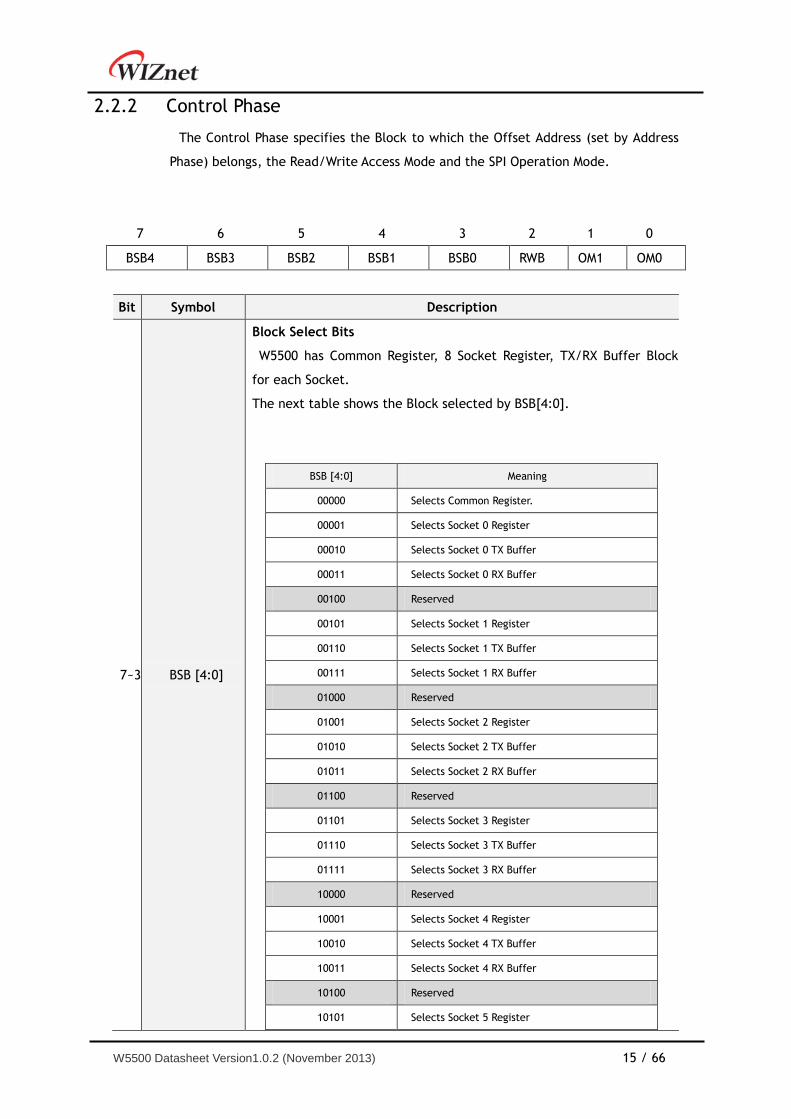
2.2.2 Control Phase
The Control Phase specifies the Block to which the Offset Address (set by Address
Phase) belongs, the Read/Write Access Mode and the SPI Operation Mode.
7 6 5 4 3 2 1 0
BSB4 BSB3 BSB2 BSB1 BSB0 RWB OM1 OM0
Bit Symbol Description
7~3 BSB [4:0]
Block Select Bits
W5500 has Common Register, 8 Socket Register, TX/RX Buffer Block
for each Socket.
The next table shows the Block selected by BSB[4:0].
BSB [4:0] Meaning
00000 Selects Common Register.
00001 Selects Socket 0 Register
00010 Selects Socket 0 TX Buffer
00011 Selects Socket 0 RX Buffer
00100 Reserved
00101 Selects Socket 1 Register
00110 Selects Socket 1 TX Buffer
00111 Selects Socket 1 RX Buffer
01000 Reserved
01001 Selects Socket 2 Register
01010 Selects Socket 2 TX Buffer
01011 Selects Socket 2 RX Buffer
01100 Reserved
01101 Selects Socket 3 Register
01110 Selects Socket 3 TX Buffer
01111 Selects Socket 3 RX Buffer
10000 Reserved
10001 Selects Socket 4 Register
10010 Selects Socket 4 TX Buffer
10011 Selects Socket 4 RX Buffer
10100 Reserved
10101 Selects Socket 5 Register

16 / 66 W5500 Datasheet Version1.0.2 (November 2013)
10110 Selects Socket 5 TX Buffer
10111 Selects Socket 5 RX Buffer
11000 Reserved
11001 Selects Socket 6 Register
11010 Selects Socket 6 TX Buffer
11011 Selects Socket 6 RX Buffer
11100 Reserved
11101 Selects Socket 7 Register
11110 Selects Socket 7 TX Buffer
11111 Selects Socket 7 RX Buffer
If the Reserved Bits are selected, it can cause the mal-function of the
W5500.
2 RWB
Read/Write Access Mode Bit
This sets Read/Write Access Mode.
‘0’ : Read
‘1’ : Write
1~0 OM [1:0]
SPI Operation Mode Bits
This sets the SPI Operation Mode.
SPI Operation Mode supports two modes, the Variable Length Data
Mode and the Fixed Length Data Mode.
- Variable Length Data Mode (VDM)
: Data Length is controlled by SCSn.
External Host makes SCSn Signal Assert (High-to-Low) and informs
the start of the SPI Frame Address Phase to W5500.
Then the external host transfers the Control Phase with
OM[1:0]=’00’.
After N-Bytes Data Phase transfers, SCSn Signal is De-asserted
(Low-to-High) and informs the end of the SPI Frame Data Phase to
W5500.
In VDM Mode, the SCSn must be controlled with SPI Frame unit by
the External Host. (Refer to the Figure 4)
W5500 Datasheet Version1.0.2 (November 2013) 17 / 66
- Fixed Length Data Mode (FDM)
: In FDM, the Data Length is set by OM[1:0], these are not ‘00’
value. So, the SCSn signal should be Low state, and has one
Length type (among 1 Bytes, 2 Bytes, 4 Bytes) according to the
OM[1:0] value. (Refer to the Figure 5.)
The next table shows the SPI Operation Mode according to the
OM[1:0].
OM[1:0] Meaning
00 Variable Data Length Mode, N-Bytes Data Phase (1 ≤ N)
01 Fixed Data Length Mode , 1 Byte Data Length (N = 1)
10 Fixed Data Length Mode , 2 Byte Data Length (N = 2)
11 Fixed Data Length Mode , 4 Byte Data Length (N = 4)
2.2.3 Data Phase
With the Control Phase set by the SPI Operation Mode Bits OM[1:0], the Data Phase
is set by two types of length, one type is the N-Bytes length (VDM mode) and the
other type is 1/2/4 Bytes (FDM mode).
At this time, 1 byte data is transferred through MOSI or MISO signal from MSB to
LSB sequentially.
2.3 Variable Length Data Mode (VDM)
In VDM mode, the SPI Frame Data Phase Length is determined by SCSn Control of
the External Host. That means that the Data Phase Length can have random value
(Any length from 1 Byte to N Bytes) according to the SCSn Control.
The OM[1:0] of the Control Phase should be ‘00’ value in VDM mode.
18 / 66 W5500 Datasheet Version1.0.2 (November 2013)
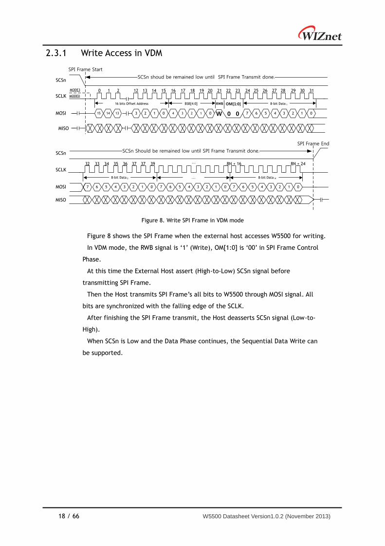
2.3.1 Write Access in VDM
Figure 8. Write SPI Frame in VDM mode
Figure 8 shows the SPI Frame when the external host accesses W5500 for writing.
In VDM mode, the RWB signal is ‘1’ (Write), OM[1:0] is ‘00’ in SPI Frame Control
Phase.
At this time the External Host assert (High-to-Low) SCSn signal before
transmitting SPI Frame.
Then the Host transmits SPI Frame’s all bits to W5500 through MOSI signal. All
bits are synchronized with the falling edge of the SCLK.
After finishing the SPI Frame transmit, the Host deasserts SCSn signal (Low-to-
High).
When SCSn is Low and the Data Phase continues, the Sequential Data Write can
be supported.
RWB
SCSn
MOSI 7 6 5 4 3 2 1 04 3 2 015 14 3 2 1 013
1 20
SCLK12 13 14 15
16 bits Offset Address BSB[4:0]
17 1816 20 21 22 23 25 2624 27 28 29 30 31
8-bit Data 1
MODE0
MODE3 19
1
MOSI 7 6 5 4 3 2 1 0 7 6 5 4 3 2 1 0 7 6 5 4 3 2 1 0
MISO
SCSn
SCLK
33 3432 35 36 37 37 39 8N + 16 8N + 24
8-bit Data 2 ... 8-bit Data N
...
OM[1:0]
MISO
W 0 0
SCSn shoud be remained low until SPI Frame Transmit done.
SCSn Should be remained low until SPI Frame Transmit done.
SPI Frame Start
SPI Frame End
W5500 Datasheet Version1.0.2 (November 2013) 19 / 66
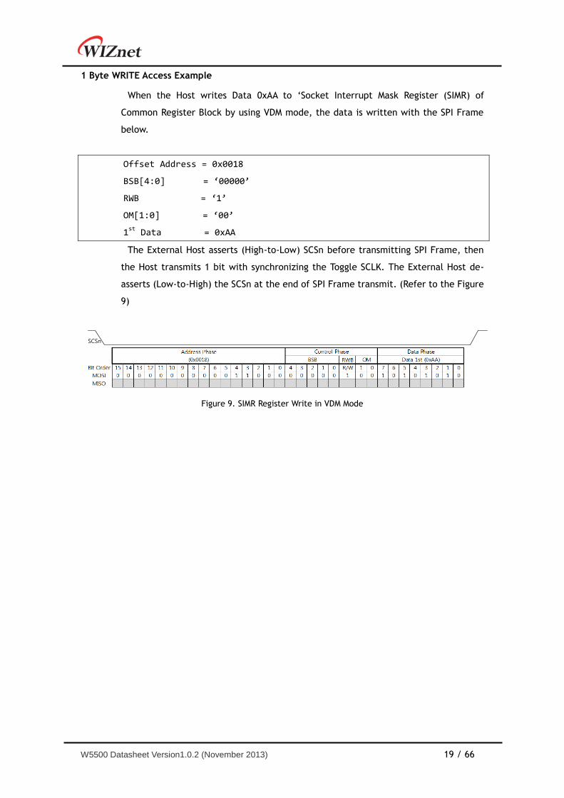
1 Byte WRITE Access Example
When the Host writes Data 0xAA to ‘Socket Interrupt Mask Register (SIMR) of
Common Register Block by using VDM mode, the data is written with the SPI Frame
below.
Offset Address = 0x0018
BSB[4:0] = ‘00000’
RWB = ‘1’
OM[1:0] = ‘00’
1st Data = 0xAA
The External Host asserts (High-to-Low) SCSn before transmitting SPI Frame, then
the Host transmits 1 bit with synchronizing the Toggle SCLK. The External Host de-
asserts (Low-to-High) the SCSn at the end of SPI Frame transmit. (Refer to the Figure
9)
Figure 9. SIMR Register Write in VDM Mode
SCSn

20 / 66 W5500 Datasheet Version1.0.2 (November 2013)
N-Bytes WRITE Access Example
When the Host writes 5 Bytes Data (0x11, 0x22, 0x33, 0x44, 0x55) to Socket 1’s TX
Buffer Block 0x0040 Address by using VDM mode, 5 bytes data are written with the SPI
Frame below.
Offset Address = 0x0040
BSB[4:0] = ‘00110’
RWB = ‘1’
OM[1:0] = ‘00’
1st Data = 0x11
2nd Data = 0x22
3rd Data = 0x33
4th Data = 0x44
5th Data = 0x55
The N-Bytes Write Access is shown in Figure 10.
The 5 bytes of Data (0x11, 0x22, 0x33, 0x44, 0x55) are written sequentially to
Socket 1’s Tx Buffer Block Address 0x0040 ~ 0x0044.
The External Host asserts (High-to-Low) SCSn before transmitting SPI Frame.
The External Host de-asserts (Low-to-High) the SCSn at the end of SPI Frame
transmit.
Figure 10. 5 Byte Data Write at 1th Socket’s TX Buffer Block 0x0040 in VDM mode
SCSn
SCSn

W5500 Datasheet Version1.0.2 (November 2013) 21 / 66
2.3.2 Read Access in VDM
Figure 11. Read SPI Frame in VDM mode
Figure 11 shows the SPI Frame when external host accesses W5500 for reading
In VDM mode, the RWB signal is ‘0’ (Write), OM[1:0] is ‘00’ in SPI Frame Control
Phase.
At this time the External Host assert (High-to-Low) SCSn signal before transmitting
SPI Frame.
Then the Host transmits Address and Control Phase all bits to W5500 through MOSI
signal. All bits are synchronized with the falling edge of the SCLK.
Then the Host receives all bits of Data Phase with synchronizing the rising edge of
Sampling SCLK through MISO signal.
After finishing the Data Phase receive, the Host deasserts SCSn signal (Low-to-
High).
When SCSn is Low and the Data Phase continues to receive, the Sequential Data
Read can be supported.
MOSI
MISO
SCSn
SCLK
33 3432 35 36 37 38 39 ... 8N + 16 8N + 24
7 6 5 4 3 2 1 0 7 6 5 4 3 2 1 0 7 6 5 4 3 2 1 0
8-bit Data 2 ... 8-bit Data N
SCSn Should be remained low until SPI Frame Transmit & Receive done.
SPI Frame End
SCSn
MOSI 4 3 2 015 14 3 2 1 013
MISO
1 20
SCLK12 13 14 15
16bits Offset Address
17 1816 20 21 22 23 25 2624 27 28 29 30 31
8-bit Data 1
MODE0
MODE3 19
1
7 6 5 4 3 2 1 0
BSB[4:0] RWB OM[1:0]
R 0 0
SCSn shoud be remained low until SPI Frame Transmit & Receive done.
SPI Frame Start
22 / 66 W5500 Datasheet Version1.0.2 (November 2013)
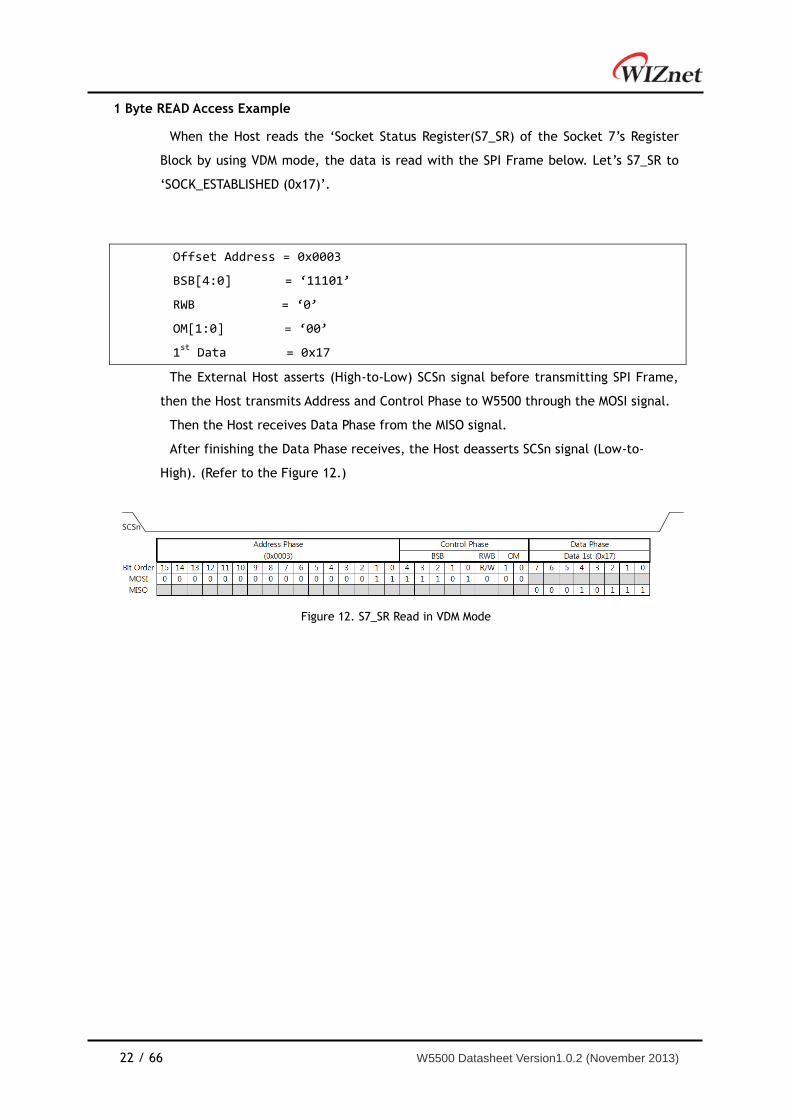
1 Byte READ Access Example
When the Host reads the ‘Socket Status Register(S7_SR) of the Socket 7’s Register
Block by using VDM mode, the data is read with the SPI Frame below. Let’s S7_SR to
‘SOCK_ESTABLISHED (0x17)’.
Offset Address = 0x0003
BSB[4:0] = ‘11101’
RWB = ‘0’
OM[1:0] = ‘00’
1st Data = 0x17
The External Host asserts (High-to-Low) SCSn signal before transmitting SPI Frame,
then the Host transmits Address and Control Phase to W5500 through the MOSI signal.
Then the Host receives Data Phase from the MISO signal.
After finishing the Data Phase receives, the Host deasserts SCSn signal (Low-to-
High). (Refer to the Figure 12.)
Figure 12. S7_SR Read in VDM Mode
SCSn

W5500 Datasheet Version1.0.2 (November 2013) 23 / 66
N-Bytes Read Access Example
When the Host reads 5 Bytes Data (0xAA, 0xBB, 0xCC, 0xDD, 0xEE) from the Socket
3’s RX Buffer Block 0x0100 Address by using VDM mode, 5 bytes data are read with the
SPI Frame as below.
Offset Address = 0x0100
BSB[4:0] = ‘01111’
RWB = ‘0’
OM[1:0] = ‘00’
1st Data = 0xAA
2nd Data = 0xBB
3rd Data = 0xCC
4th Data = 0xDD
5th Data = 0xEE
The N-Bytes Read Access is shown in Figure 13.
The 5 bytes of Data (0xAA, 0xBB, 0xCC, 0xDD, 0xEE) are read sequentially from the
Socket 3’s Rx Buffer Block Address 0x0100 ~ 0x0104.
The External Host asserts (High-to-Low) SCSn before transmitting SPI Frame.
The External Host de-asserts (Low-to-High) the SCSn at the end of the SPI Frame
Data Phase.
Figure 13. 5 Byte Data Read at Socket 3 RX Buffer Block 0x0100 in VDM mode
SCSn
SCSn

24 / 66 W5500 Datasheet Version1.0.2 (November 2013)
2.4 Fixed Length Data Mode (FDM)
The FDM mode can be used when the External Host cannot control SCSn signal.
The SCSn signal should be tied to Low (Always connected to GND) and it is not
possible to share the SPI Bus with other SPI Devices. (Refer to the Figure 5.)
In VDM mode, Data Phase length is controlled by SCSn control.
But in FDM mode, Data Phase length is controlled by OM[1:0] value (‘01’ / ‘10’ / ‘11’)
which is the SPI Operation Mode Bits of the Control Phase.
As the SPI Frame of FDM mode is the same as SPI Frame of VDM mode (1Byte, 2
Bytes, 4 Bytes SPI Frame) except for the SCSn signal control and OM[1:0] setting, the
detail about FDM mode is not described in this section.
It is not recommended to use the FDM mode unless you are in inevitable status. In
addition, we use only 1/2/4 Bytes SPI Frame, as described in ‘Chapter 2.4.1’ &
‘Chapter 2.4.2’. Using SPI Frame with other length of Data will cause malfunction of
W5500.
W5500 Datasheet Version1.0.2 (November 2013) 25 / 66
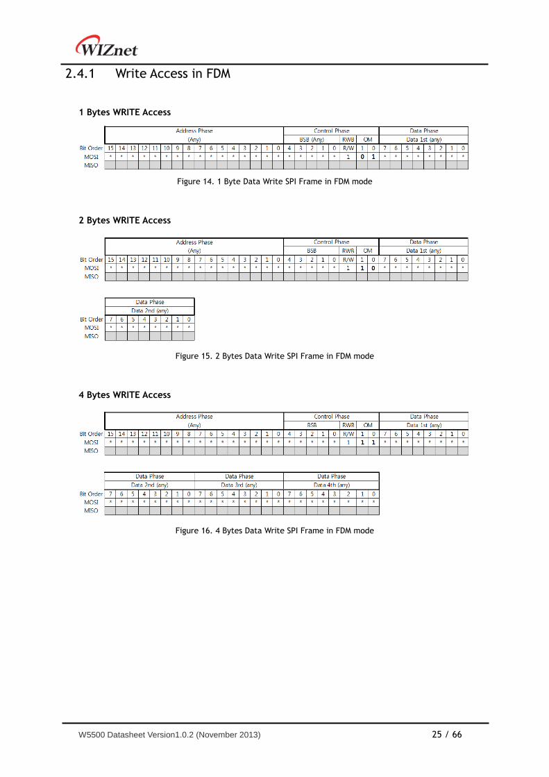
2.4.1 Write Access in FDM
1 Bytes WRITE Access
Figure 14. 1 Byte Data Write SPI Frame in FDM mode
2 Bytes WRITE Access
Figure 15. 2 Bytes Data Write SPI Frame in FDM mode
4 Bytes WRITE Access
Figure 16. 4 Bytes Data Write SPI Frame in FDM mode

26 / 66 W5500 Datasheet Version1.0.2 (November 2013)
2.4.2 Read Access in FDM
1 Byte READ Access
Figure 17. 1 Byte Data Read SPI Frame in FDM mode
2 Bytes READ Access
Figure 18. 2 Bytes Data Read SPI Frame in FDM mode
4 Bytes READ Access
Figure 19. 4 Bytes Data Read SPI Frame in FDM mode

W5500 Datasheet Version1.0.2 (November 2013) 27 / 66
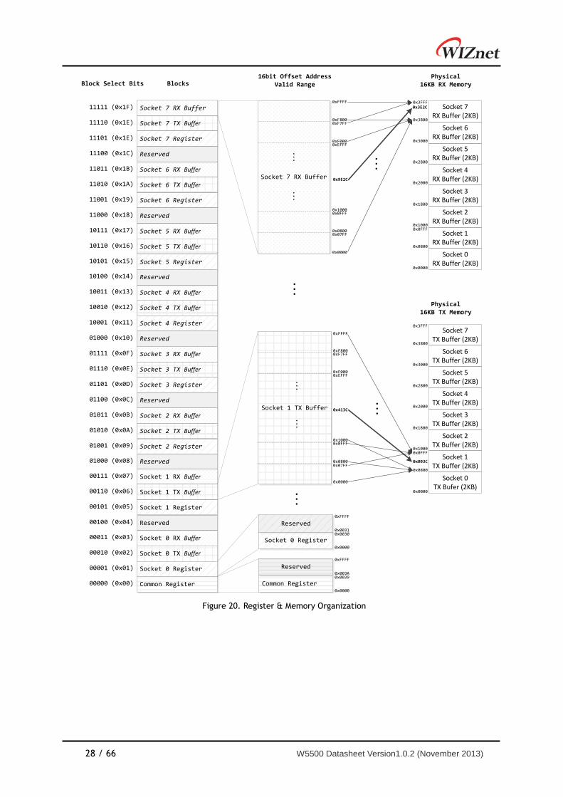
Register and Memory Organization 3
W5500 has one Common Register Block, eight Socket Register Blocks, and TX/RX
Buffer Blocks allocated to each Socket. Each block is selected by the BSB[4:0](Block
Select Bit) of SPI Frame. Figure 20 shows the selected block by the BSB[4:0] and the
available offset address range of Socket TX/RX Buffer Blocks. Each Socket’s TX Buffer
Block exists in one 16KB TX memory physically and is initially allocated with 2KB.
Also, Each Socket’s RX Buffer Block exists in one 16KB RX Memory physically and is
initially allocated with 2KB.
Regardless of the allocated size of each Socket TX/RX Buffer, it can be accessible
within the 16 bits offset address range (From 0x0000 to 0xFFFF).
Refer to ‘Chapter 3.3’ for more information about 16KB TX/RX Memory
organization and access method.
28 / 66 W5500 Datasheet Version1.0.2 (November 2013)
Figure 20. Register & Memory Organization
Block Select Bits BlocksPhysical
16KB RX Memory16bit Offset Address
Valid Range
...
11111 (0x1F)
11110 (0x1E)
11101 (0x1E)
11100 (0x1C)
11011 (0x1B)
11010 (0x1A)
11001 (0x19)
11000 (0x18)
10111 (0x17)
10110 (0x16)
10101 (0x15)
10011 (0x13)
10010 (0x12)
10001 (0x11)
01000 (0x10)
01111 (0x0F)
01110 (0x0E)
01101 (0x0D)
01100 (0x0C)
01011 (0x0B)
01010 (0x0A)
01001 (0x09)
01000 (0x08)
00111 (0x07)
00110 (0x06)
00101 (0x05)
00011 (0x03)
00010 (0x02)
00001 (0x01)
00000 (0x00)
00100 (0x04)
10100 (0x14)
Socket 7 RX Buffer
Socket 7 TX Buffer
Socket 7 Register
Reserved
Socket 6 RX Buffer
Socket 6 TX Buffer
Socket 6 Register
Reserved
Socket 5 RX Buffer
Socket 5 TX Buffer
Socket 5 Register
Socket 4 RX Buffer
Socket 4 TX Buffer
Socket 4 Register
Reserved
Socket 3 RX Buffer
Socket 3 TX Buffer
Socket 3 Register
Reserved
Socket 2 RX Buffer
Socket 2 TX Buffer
Socket 2 Register
Reserved
Socket 1 RX Buffer
Socket 1 TX Buffer
Socket 1 Register
Reserved
Socket 0 RX Buffer
Socket 0 TX Buffer
Socket 0 Register
Common Register
Reserved
Common Register0x0000
Reserved
0x00390x003A
0xFFFF
Socket 0 Register
Reserved
0x0000
0x00300x0031
0xFFFF
Socket 1 TX Buffer
0x0000
0x07FF0x0800
0xFFFF
0x0FFF0x1000
...
0xEFFF0xF000
0xF7FF0xF800
...
Socket 7 RX Buffer
...
0x0000
0x07FF0x0800
0xFFFF
0x0FFF0x1000
0xEFFF0xF000
0xF7FF0xF800
...
...
...0x413C
0x0000
0x1000
0x0800
0x1800
0x2000
0x2800
0x3000
0x3800
0x3FFF
Socket 0TX Bufer (2KB)
Socket 1TX Buffer (2KB)
Socket 2TX Buffer (2KB)
Socket 3TX Buffer (2KB)
Socket 4TX Buffer (2KB)
Socket 5TX Buffer (2KB)
Socket 6TX Buffer (2KB)
Socket 7TX Buffer (2KB)
0x093C
0x0FFF
...
0x9E2C
0x0000
0x1000
0x0800
0x1800
0x2000
0x2800
0x3000
0x3800
0x3FFF
Socket 0RX Buffer (2KB)
Socket 1RX Buffer (2KB)
Socket 2RX Buffer (2KB)
Socket 3RX Buffer (2KB)
Socket 4RX Buffer (2KB)
Socket 5RX Buffer (2KB)
Socket 6RX Buffer (2KB)
Socket 7 RX Buffer (2KB)
0x3E2C
0x0FFF
Physical 16KB TX Memory
W5500 Datasheet Version1.0.2 (November 2013) 29 / 66
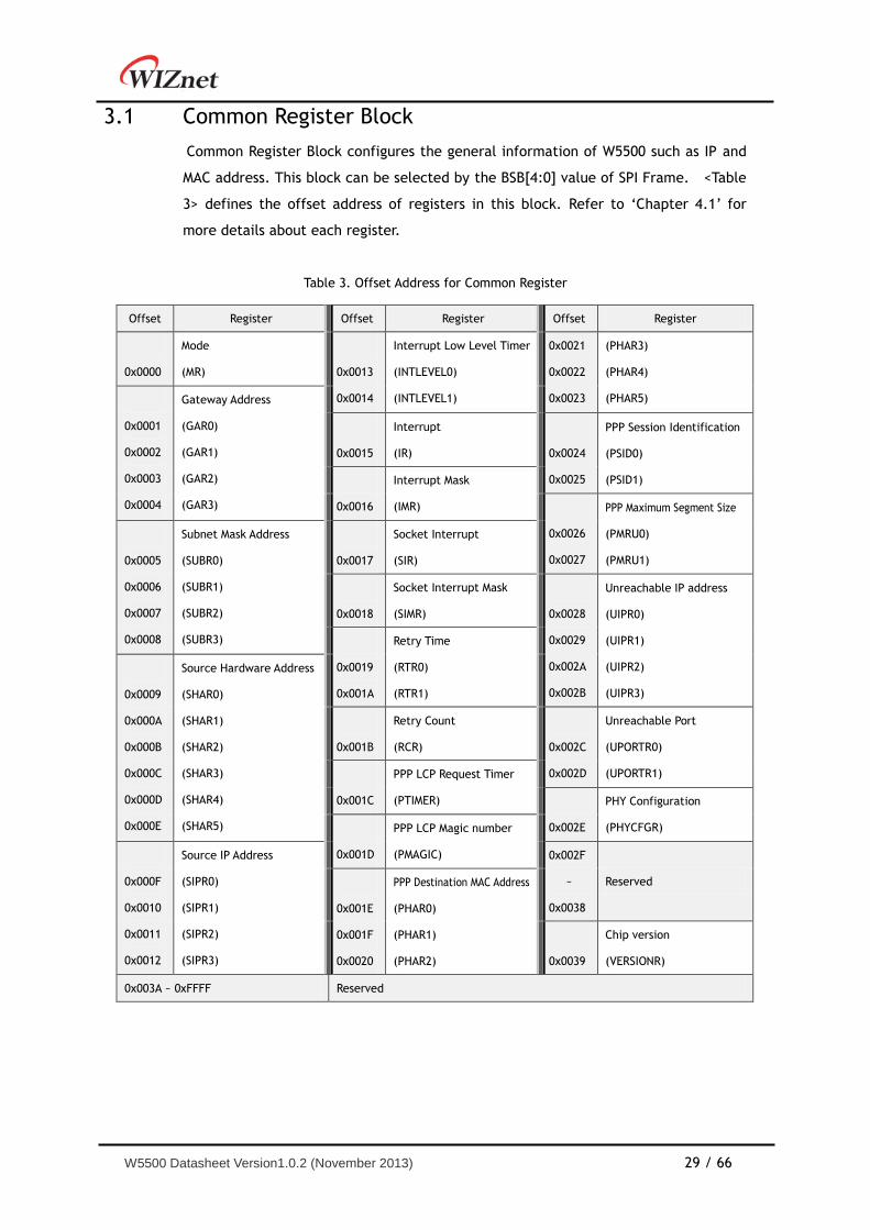
3.1 Common Register Block
Common Register Block configures the general information of W5500 such as IP and
MAC address. This block can be selected by the BSB[4:0] value of SPI Frame. <Table
3> defines the offset address of registers in this block. Refer to ‘Chapter 4.1’ for
more details about each register.
Table 3. Offset Address for Common Register
Offset Register Offset Register Offset Register
0x0000
Mode
(MR)
0x0013
0x0014
Interrupt Low Level Timer
(INTLEVEL0)
(INTLEVEL1)
0x0021
0x0022
0x0023
(PHAR3)
(PHAR4)
(PHAR5)
0x0001
0x0002
0x0003
0x0004
Gateway Address
(GAR0)
(GAR1)
(GAR2)
(GAR3)
0x0015
Interrupt
(IR)
0x0024
0x0025
PPP Session Identification
(PSID0)
(PSID1)
0x0016
Interrupt Mask
(IMR)
0x0026
0x0027
PPP Maximum Segment Size
(PMRU0)
(PMRU1)
0x0005
0x0006
0x0007
0x0008
Subnet Mask Address
(SUBR0)
(SUBR1)
(SUBR2)
(SUBR3)
0x0017
Socket Interrupt
(SIR)
0x0018
Socket Interrupt Mask
(SIMR)
0x0028
0x0029
0x002A
0x002B
Unreachable IP address
(UIPR0)
(UIPR1)
(UIPR2)
(UIPR3)
0x0019
0x001A
Retry Time
(RTR0)
(RTR1)
0x0009
0x000A
0x000B
0x000C
0x000D
0x000E
Source Hardware Address
(SHAR0)
(SHAR1)
(SHAR2)
(SHAR3)
(SHAR4)
(SHAR5)
0x001B
Retry Count
(RCR)
0x002C
0x002D
Unreachable Port
(UPORTR0)
(UPORTR1)
0x001C
PPP LCP Request Timer
(PTIMER)
0x002E
PHY Configuration
(PHYCFGR)
0x001D
PPP LCP Magic number
(PMAGIC)
0x000F
0x0010
0x0011
0x0012
Source IP Address
(SIPR0)
(SIPR1)
(SIPR2)
(SIPR3)
0x002F
~
0x0038
Reserved
0x001E
0x001F
0x0020
PPP Destination MAC Address
(PHAR0)
(PHAR1)
(PHAR2)
0x0039
Chip version
(VERSIONR)
0x003A ~ 0xFFFF Reserved

30 / 66 W5500 Datasheet Version1.0.2 (November 2013)
3.2 Socket Register Block
W5500 supports 8 Sockets for communication channel. Each Socket is controlled by Socket n
Register Block(when 0≤n≤7). The n value of Socket n Register can be selected by BSB[4:0] of
SPI Frame. <Table 4> defines the 16bits Offset Address of registers in Socket n Register Block.
Refer to ‘Chapter 4.2’ for more details about each register.
Table 4. Offset Address in Socket n Register Block (0≤n≤7)
Offset Register Offset Register Offset Register
0x0000
Socket n Mode
(Sn_MR)
0x0010
0x0011
Socket n Destination Port
(Sn_DPORT0)
(Sn_DPORT1)
0x0024
0x0025
Socket n TX Write
Pointer
(Sn_TX_WR0)
(Sn_TX_WR1)
0x0001
Socket n Command (Sn_CR)
0x0012
0x0013
Socket n
Maximum Segment Size
(Sn_MSSR0)
(Sn_MSSR1)
0x0026
0x0027
Socket n RX Received
Size
(Sn_RX_RSR0)
(Sn_RX_RSR1)
0x0002
Socket n Interrupt
(Sn_IR)
0x0003
Socket n Status
(Sn_SR)
0x0028
0x0029
Socket n RX Read
Pointer
(Sn_RX_RD0)
(Sn_RX_RD1)
0x0014 Reserved
0x0004
0x0005
Socket n Source Port
(Sn_PORT0)
(Sn_PORT1)
0x0015 Socket n IP TOS
(Sn_TOS)
0x002A
0x002B
Socket n RX Write
Pointer
(Sn_RX_WR0)
(Sn_RX_WR1)
0x0016
Socket n IP TTL
(Sn_TTL)
0x0006
0x0007
0x0008
0x0009
0x000A
0x000B
Socket n Destination
Hardware Address
(Sn_DHAR0)
(Sn_DHAR1)
(Sn_DHAR2)
(Sn_DHAR3)
(Sn_DHAR4)
(Sn_DHAR5)
0x0017
~
0x001D
Reserved
0x002C
Socket n Interrupt Mask
(Sn_IMR)
0x002D
0x002E
Socket n Fragment
Offset in IP header
(Sn_FRAG0)
(Sn_FRAG1)
0x001E
Socket n Receive Buffer
Size
(Sn_RXBUF_SIZE)
0x001F
Socket n
Transmit Buffer Size
(Sn_TXBUF_SIZE)
0x002F
Keep alive timer
(Sn_KPALVTR)
0x000C
0x000D
0x000E
0x000F
Socket n
Destination IP Address
(Sn_DIPR0)
(Sn_DIPR1)
(Sn_DIPR2)
(Sn_DIPR3)
0x0020
0x0021
Socket n TX Free Size
(Sn_TX_FSR0)
(Sn_TX_FSR1)
0x0030
~
0xFFFF
Reserved
0x0022
0x0023
Socket n TX Read Pointer
(Sn_TX_RD0)
(Sn_TX_RD1)

W5500 Datasheet Version1.0.2 (November 2013) 31 / 66
3.3 Memory
W5500 has one 16KB TX memory for Socket n TX Buffer Blocks and one 16KB RX
memory for Socket n RX buffer Blocks.
16KB TX memory is initially allocated in 2KB size for each Socket TX Buffer Block
(2KB X 8 = 16KB). The initial allocated 2KB size of Socket n TX Buffer can be re-
allocated by using ‘Socket n TX Buffer Size Register (Sn_TXBUF_SIZE)’.
Once all Sn_TXBUF_SIZE registers have been configured, Socket TX Buffer is allocated
with the configured size of 16KB TX Memory and is assigned sequentially from Socket
0 to Socket 7. Its physical memory address is automatically determined in 16KB TX
memory. Therefore, the total sum of Sn_TXBUF_SIZE should be not exceed 16 in case
of error in data transmission.
The 16KB RX memory allocation method is the same as the 16KB TX memory
allocation method. 16KB RX memory is initially allocated into 2KB size for each
Socket RX Buffer Block (2KB X 8 = 16KB). The initial allocated 2KB size of Socket n RX
Buffer can be re-allocated by using ‘Socket n RX Buffer Size Register
(Sn_RXBUF_SIZE)’.
When all Sn_RXBUF_SIZE registers have been configured, the Socket RX Buffer is
allocated with the configured size in 16KB RX Memory and is assigned sequentially
from Socket 0 to Socket 7. The physical memory address of the Socket RX Buffer is
automatically determined in 16KB RX memory. Therefore, the total sum of
Sn_RXBUF_SIZE should not exceed 16, data reception error will occur if exceeded.
For 16KB TX/RX memory allocation, refer to Sn_TXBUF_SIZE & Sn_RXBUF_SIZE in
‘Chapter 4.2’.
The Socket n TX Buffer Block allocated in 16KB TX memory is buffer for saving data
to be transmitted by host. The 16bits Offset Address of Socket n TX Buffer Block has
64KB address space ranged from 0x0000 to 0xFFFF, and it is configured with
reference to ‘Socket n TX Write Pointer Register (Sn_TX_WR)’ & ‘Socket n TX Read
Pointer Register(Sn_RX_RD)’. However, the 16bits Offset Address automatically
converts into the physical address to be accessible in 16KB TX memory such as Figure
20. Refer to ‘Chapter 4.2’ for Sn_TX_WR & Sn_TX_RD.
The Socket n RX Buffer Block allocated in 16KB RX memory is buffer for saving the
received data through the Ethernet. The 16bits Offset Address of Socket n RX Buffer
Block has 64KB address space ranged from 0x0000 to 0xFFFF, and it is configured with
reference to ‘Socket n RX RD Pointer Register (Sn_RX_RD)’ & ‘Socket n RX Write
Pointer Register (Sn_RX_WR)’. However, the 16bits Offset Address automatically
converts into the physical address to be accessible in 16KB RX memory such as Figure
20. Refer to ‘Chapter 4.2’ for Sn_RX_RD & Sn_RX_WR.
32 / 66 W5500 Datasheet Version1.0.2 (November 2013)
Register Descriptions 4
4.1 Common Registers
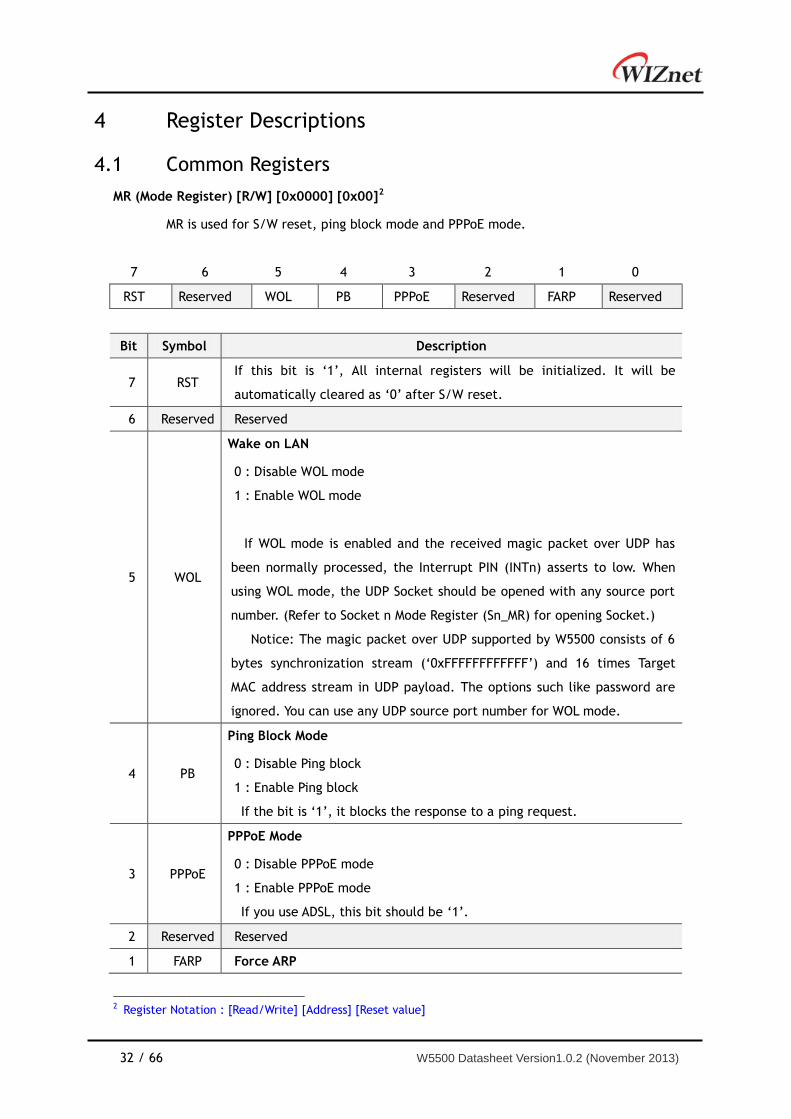
MR (Mode Register) [R/W] [0x0000] [0x00]2
MR is used for S/W reset, ping block mode and PPPoE mode.
7 6 5 4 3 2 1 0
RST Reserved WOL PB PPPoE Reserved FARP Reserved
Bit Symbol Description
7 RST If this bit is ‘1’, All internal registers will be initialized. It will be
automatically cleared as ‘0’ after S/W reset.
6 Reserved Reserved
5 WOL
Wake on LAN
0 : Disable WOL mode
1 : Enable WOL mode
If WOL mode is enabled and the received magic packet over UDP has
been normally processed, the Interrupt PIN (INTn) asserts to low. When
using WOL mode, the UDP Socket should be opened with any source port
number. (Refer to Socket n Mode Register (Sn_MR) for opening Socket.)
Notice: The magic packet over UDP supported by W5500 consists of 6
bytes synchronization stream (‘0xFFFFFFFFFFFF’) and 16 times Target
MAC address stream in UDP payload. The options such like password are
ignored. You can use any UDP source port number for WOL mode.
4 PB
Ping Block Mode
0 : Disable Ping block
1 : Enable Ping block
If the bit is ‘1’, it blocks the response to a ping request.
3 PPPoE
PPPoE Mode
0 : Disable PPPoE mode
1 : Enable PPPoE mode
If you use ADSL, this bit should be ‘1’.
2 Reserved Reserved
1 FARP Force ARP
2 Register Notation : [Read/Write] [Address] [Reset value]
W5500 Datasheet Version1.0.2 (November 2013) 33 / 66
0 : Disable Force ARP mode
1 : Enable Force ARP mode
In Force ARP mode, It forces on sending ARP Request whenever data is
sent.
0 Reserved Reserved
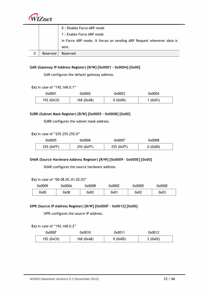
GAR (Gateway IP Address Register) [R/W] [0x0001 – 0x0004] [0x00]
GAR configures the default gateway address.
Ex) In case of “192.168.0.1”
0x0001 0x0002 0x0003 0x0004
192 (0xC0) 168 (0xA8) 0 (0x00) 1 (0x01)
SUBR (Subnet Mask Register) [R/W] [0x0005 – 0x0008] [0x00]
SUBR configures the subnet mask address.
Ex) In case of “255.255.255.0”
0x0005 0x0006 0x0007 0x0008
255 (0xFF) 255 (0xFF) 255 (0xFF) 0 (0x00)
SHAR (Source Hardware Address Register) [R/W] [0x0009 – 0x000E] [0x00]
SHAR configures the source hardware address.
Ex) In case of “00.08.DC.01.02.03”
0x0009 0x000A 0x000B 0x000C 0x000D 0x000E
0x00 0x08 0xDC 0x01 0x02 0x03
SIPR (Source IP Address Register) [R/W] [0x000F – 0x0012] [0x00]
SIPR configures the source IP address.
Ex) In case of “192.168.0.2”
0x000F 0x0010 0x0011 0x0012
192 (0xC0) 168 (0xA8) 0 (0x00) 2 (0x02)

34 / 66 W5500 Datasheet Version1.0.2 (November 2013)
INTLEVEL (Interrupt Low Level Timer Register) [R/W] [0x0013 – 0x0014] [0x0000]
INTLEVEL configures the Interrupt Assert Wait Time (IAWT). When the next interrupt
occurs, Interrupt PIN (INTn ) will assert to low after INTLEVEL time.
𝐼𝐴𝑊𝑇 = (𝐼𝑁𝑇𝐿𝐸𝑉𝐸𝐿 + 1) × 𝑃𝐿𝐿𝐶𝐿𝐾 × 4 (when INTLEVEL > 0)
Figure 21. INTLEVEL Timing
a. When Timeout Interrupt of Socket 0 is occurred, S0_IR[3] & SIR[0] bit set as ‘1’
and then INTn PIN is asserted to low.
b. When the connection interrupt of Socket 1 is occurred before the previous
interrupt processing is not completed, S1_IR[0] & SIR[1] bits set as ‘1’ and INTn PIN is
still low.
c. If the host processed the previous interrupt completely by clearing the S0_IR[3]
bit, INTn PIN is de-asserted to high but S1_IR[0] & SIR[1] is still set as ‘1’.
d. Although S1_IR[0] & SIR[1] bit is set as ‘1’, the INTn can’t be asserted to low
during INTLEVEL time. After the INTLEVEL time expires, the INTn will be asserted to
low.
PLL_CLK
SIR
S0_IR
S1_IR
0x0000 0x0001 0x0002
0x04 0x00
0x01
0x00
0x00
1 2 3 4 5 6 7 8 9 10 11 12 13 14 15 16
0x0003
INTn
a.
b.
c. d.IAWT

W5500 Datasheet Version1.0.2 (November 2013) 35 / 66
IR (Interrupt Register) [R/W] [0x0015] [0x00]
IR indicates the interrupt status. Each bit of IR can be cleared when the host writes
‘1’ value to each bit. If IR is not equal to ‘0x00’, INTn PIN is asserted low until it is
‘0x00’.
7 6 5 4 3 2 1 0
CONFLICT UNREACH PPPoE MP Reserved Reserved Reserved Reserved
Bit Symbol Description
7 CONFLICT
IP Conflict
Bit is set as ‘1’ when own source IP address is same with the sender
IP address in the received ARP request.
6 UNREACH
Destination unreachable
When receiving the ICMP (Destination port unreachable) packet, this
bit is set as ‘1’.
When this bit is ‘1’, Destination Information such as IP address and
Port number may be checked with the corresponding UIPR &
UPORTR.
5 PPPoE PPPoE Connection Close
When PPPoE is disconnected during PPPoE mode, this bit is set.
4 MP
Magic Packet
When WOL mode is enabled and receives the magic packet over UDP,
this bit is set.
3~0 Reserved Reserved

36 / 66 W5500 Datasheet Version1.0.2 (November 2013)
IMR (Interrupt Mask Register) [R/W][0x0016][0x00]
IMR is used to mask interrupts. Each bit of IMR corresponds to each bit of IR. When
a bit of IMR is ‘1’ and the corresponding bit of IR is ‘1’, an interrupt will be issued.
In other words, if a bit of IMR is ‘0’, an interrupt will not be issued even if the
corresponding bit of IR is ‘1’.
7 6 5 4 3 2 1 0
IM_IR7 IM_IR6 IM_IR5 IM_IR4 Reserved Reserved Reserved Reserved
Bit Symbol Description
7 IM_IR7
IP Conflict Interrupt Mask
0: Disable IP Conflict Interrupt
1: Enable IP Conflict Interrupt
6 IM_IR6
Destination unreachable Interrupt Mask
0: Disable Destination unreachable Interrupt
1: Enable Destination unreachable Interrupt
5 IM_IR5
PPPoE Close Interrupt Mask
0: Disable PPPoE Close Interrupt
1: Enable PPPoE Close Interrupt
4 IM_IR4
Magic Packet Interrupt Mask
0: Disable Magic Packet Interrupt
1: Enable Magic Packet Interrupt
3~0 Reserved Reserved

W5500 Datasheet Version1.0.2 (November 2013) 37 / 66
SIR (Socket Interrupt Register) [R/W] [0x0017] [0x00]
SIR indicates the interrupt status of Socket. Each bit of SIR be still ‘1’ until Sn_IR is
cleared by the host. If Sn_IR is not equal to ‘0x00’, the n-th bit of SIR is ‘1’ and INTn
PIN is asserted until SIR is ‘0x00’.
7 6 5 4 3 2 1 0
S7_INT S6_INT S5_INT S4_INT S3_INT S2_INT S1_INT S0_INT
Bit Symbol Description
7
~
0
Sn_INT
When the interrupt of Socket n occurs, the n-th bit of SIR becomes
‘1’.
SIMR (Socket Interrupt Mask Register) [R/W] [0x0018] [0x00]
Each bit of SIMR corresponds to each bit of SIR. When a bit of SIMR is ‘1’ and the
corresponding bit of SIR is ‘1’, Interrupt will be issued. In other words, if a bit of
SIMR is ‘0’, an interrupt will be not issued even if the corresponding bit of SIR is ‘1’.
7 6 5 4 3 2 1 0
S7_IMR S6_IMR S5_IMR S4_IMR S3_IMR S2_IMR S1_IMR S0_IMR
Bit Symbol Description
7
~
0
Sn_IMR
Socket n(Sn_INT) Interrupt Mask
0: Disable Socket n Interrupt
1: Enable Socket n Interrupt

38 / 66 W5500 Datasheet Version1.0.2 (November 2013)
RTR (Retry Time-value Register) [R/W] [0x0019 – 0x001A] [0x07D0]
RTR configures the retransmission timeout period. The unit of timeout period is
100us and the default of RTR is ‘0x07D0’ or ‘2000’. And so the default timeout period
is 200ms(100us X 2000).
During the time configured by RTR, W5500 waits for the peer response to the
packet that is transmitted by Sn_CR(CONNECT, DISCON, CLOSE, SEND, SEND_MAC,
SEND_KEEP command). If the peer does not respond within the RTR time, W5500
retransmits the packet or issues timeout.
Ex) When timeout-period is set as 400ms, RTR = (400ms / 1ms) X 10 = 4000(0x0FA0)
0x0019 0x001A
0x0F 0xA0
RCR (Retry Count Register) [R/W] [0x001B] [0x08]
RCR configures the number of time of retransmission. When retransmission occurs
as many as ‘RCR+1’, Timeout interrupt is issued (Sn_IR[TIMEOUT] = ‘1’).
Ex) RCR = 0x0007
0x001B
0x07
The timeout of W5500 can be configurable with RTR and RCR. W5500 has two kind
timeout such as Address Resolution Protocol (ARP) and TCP retransmission.
At the ARP (Refer to RFC 826, http://www.ietf.org/rfc.html) retransmission
timeout, W5500 automatically sends ARP-request to the peer’s IP address in order to
acquire MAC address information (used for communication of IP, UDP, or TCP). While
waiting for ARP-response from the peer, if there is no response during the configured
RTR time, a temporary timeout is occurred and ARP-request is retransmitted. It is
repeated as many as ‘RCR + 1’ times. Even after the ARP-request retransmissions are
repeated as ‘RCR+1’ and there is no response to the ARP-request, the final timeout is
occurred and Sn_IR(TIMEOUT) becomes ‘1’. The time of final timeout (ARPTO) of ARP-
request is as below.
𝐴𝑅𝑃𝑇𝑂 = (𝑅𝑇𝑅 × 0.1𝑚𝑠) × (𝑅𝐶𝑅 + 1)
At the TCP packet retransmission timeout, W5500 transmits TCP packets (SYN, FIN,
RST, DATA packets) and waits for the acknowledgement (ACK) during the configured
RTR time and RCR. If there is no ACK from the peer, a temporary timeout occurs and

W5500 Datasheet Version1.0.2 (November 2013) 39 / 66
the TCP packet is retransmitted. The retransmission is repeated as many as ‘RCR+1’.
Even after TCP retransmission is repeated as ‘RCR+1’ and there is no response to the
TCP retransmission, the final timeout is occurred and Sn_IR(TIMEOUT) becomes ‘1’.
The time of final timeout (TCPTO) of TCP retransmission is as below.
𝑇𝐶𝑃𝑇𝑂 = (∑(𝑅𝑇𝑅 × 2𝑁) + ((𝑅𝐶𝑅 − 𝑀) × 𝑅𝑇𝑅𝑀𝐴𝑋)
𝑀
𝑁=0
) × 0.1𝑚𝑠
N : Retransmission count, 0≤N ≤ M
M : Minimum value when RTR x 2(M+1) > 65535 and 0 ≤ M ≤ RCR
RTRMAX : RTR x 2M
Ex) When RTR = 2000(0x07D0), RCR = 8(0x0008),
ARPTO = 2000 X 0.1ms X 9 = 1800ms = 1.8s
TCPTO = (0x07D0+0x0FA0+0x1F40+0x3E80+0x7D00+0xFA00+0xFA00+0xFA00+0xFA00) X 0.1ms
= (2000 + 4000 + 8000 + 16000 + 32000 + ((8 - 4) X 64000)) X 0.1ms
= 318000 X 0.1ms = 31.8s
PTIMER (PPP Link Control Protocol Request Timer Register) [R/W] [0x001C] [0x0028]
PTIMER configures the time for sending LCP echo request. The unit of time is 25ms.
Ex) in case that PTIMER is 200,
200 * 25(ms) = 5000(ms) = 5 seconds
PMAGIC (PPP Link Control Protocol Magic number Register) [R/W] [0x001D] [0x00]
PMAGIC configures the 4bytes magic number to be used in LCP echo request.
Ex) PMAGIC = 0x01
0x001D
0x01
LCP Magic number = 0x01010101
40 / 66 W5500 Datasheet Version1.0.2 (November 2013)
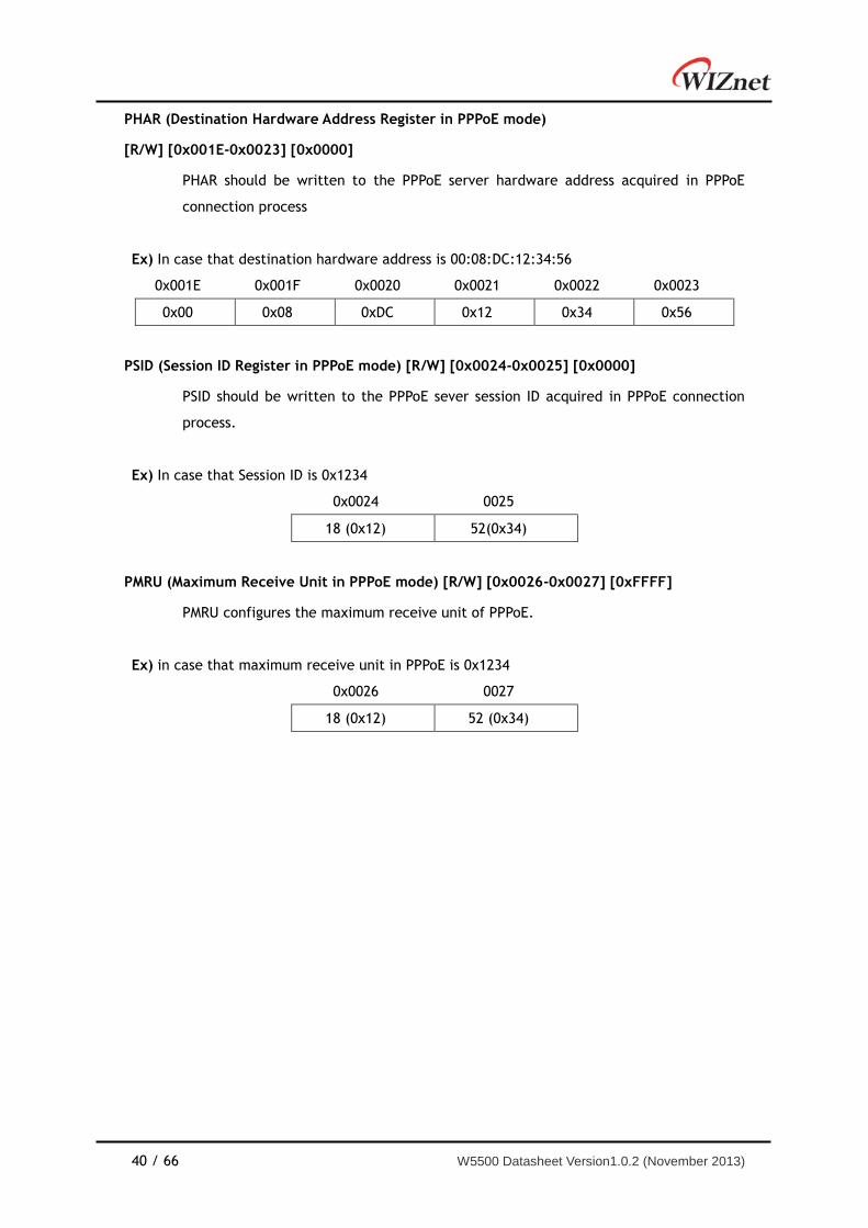
PHAR (Destination Hardware Address Register in PPPoE mode)
[R/W] [0x001E-0x0023] [0x0000]
PHAR should be written to the PPPoE server hardware address acquired in PPPoE
connection process
Ex) In case that destination hardware address is 00:08:DC:12:34:56
0x001E 0x001F 0x0020 0x0021 0x0022 0x0023
0x00 0x08 0xDC 0x12 0x34 0x56
PSID (Session ID Register in PPPoE mode) [R/W] [0x0024-0x0025] [0x0000]
PSID should be written to the PPPoE sever session ID acquired in PPPoE connection
process.
Ex) In case that Session ID is 0x1234
0x0024 0025
18 (0x12) 52(0x34)
PMRU (Maximum Receive Unit in PPPoE mode) [R/W] [0x0026-0x0027] [0xFFFF]
PMRU configures the maximum receive unit of PPPoE.
Ex) in case that maximum receive unit in PPPoE is 0x1234
0x0026 0027
18 (0x12) 52 (0x34)
W5500 Datasheet Version1.0.2 (November 2013) 41 / 66
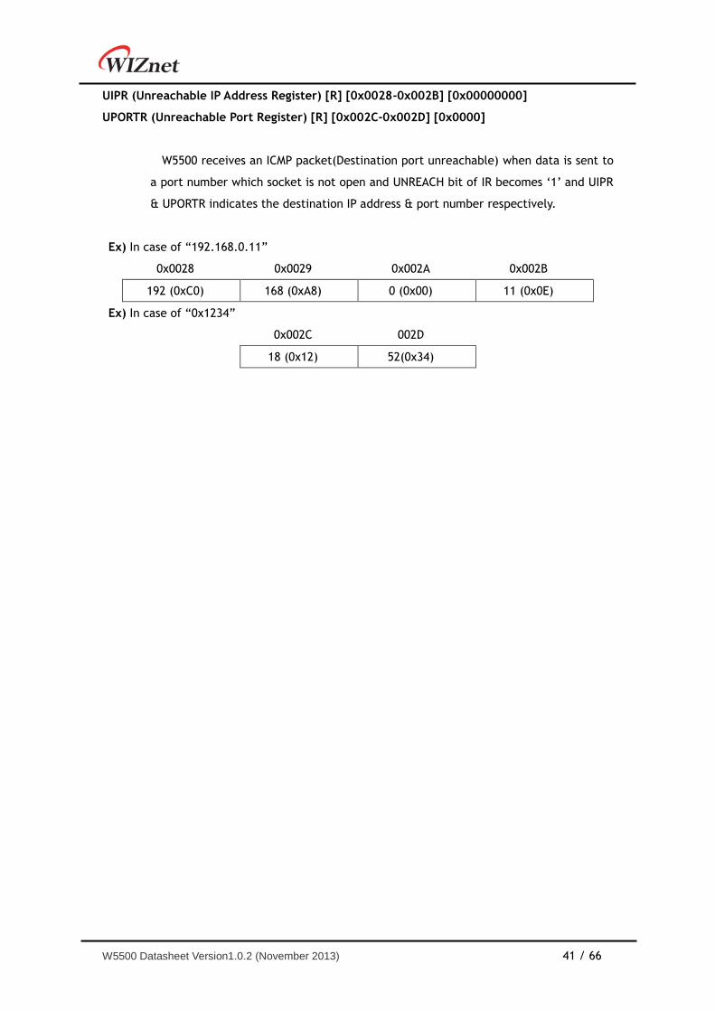
UIPR (Unreachable IP Address Register) [R] [0x0028-0x002B] [0x00000000]
UPORTR (Unreachable Port Register) [R] [0x002C-0x002D] [0x0000]
W5500 receives an ICMP packet(Destination port unreachable) when data is sent to
a port number which socket is not open and UNREACH bit of IR becomes ‘1’ and UIPR
& UPORTR indicates the destination IP address & port number respectively.
Ex) In case of “192.168.0.11”
0x0028 0x0029 0x002A 0x002B
192 (0xC0) 168 (0xA8) 0 (0x00) 11 (0x0E)
Ex) In case of “0x1234”
0x002C 002D
18 (0x12) 52(0x34)

42 / 66 W5500 Datasheet Version1.0.2 (November 2013)
PHYCFGR (W5500 PHY Configuration Register) [R/W] [0x002E] [0b10111XXX]
PHYCFGR configures PHY operation mode and resets PHY. In addition, PHYCFGR
indicates the status of PHY such as duplex, Speed, Link.
Bit Symbol Description
7 RST
Reset [R/W]
When this bit is ‘0’, internal PHY is reset.
After PHY reset, it should be set as ‘1’.
6 OPMD
Configure PHY Operation Mode
1: Configure with OPMDC[2:0] in PHYCFGR
0: Configure with the H/W PINs(PMODE[2:0])
This bit configures PHY operation mode with OPMDC[2:0] bits or
PMODE[2:0] PINs. When W5500 is reset by POR or RSTn PIN, PHY
operation mode is configured with PMODE[2:0] PINs by default. After
POR or RSTn reset, user can re-configure PHY operation mode with
OPMDC[2:0]. If user wants to re-configure with PMDC[2:0], it should
reset PHY by setting the RST bit to ‘0’ after the user configures this
bit as ‘1’ and OPMDC[2:0] .
5~3 OPMDC
Operation Mode Configuration Bit[R/W]
These bits select the operation mode of PHY such as following table.
5 4 3 Description
0 0 0 10BT Half-duplex, Auto-negotiation disabled
0 0 1 10BT Full-duplex, Auto-negotiation disabled
0 1 0 100BT Half-duplex, Auto-negotiation disabled
0 1 1 100BT Full-duplex, Auto-negotiation disabled
1 0 0 100BT Half-duplex, Auto-negotiation enabled
1 0 1 Not used
1 1 0 Power Down mode
1 1 1 All capable, Auto-negotiation enabled
2 DPX Duplex Status [Read Only]
1: Full duplex
0: Half duplex
1 SPD Speed Status [Read Only]
1: 100Mpbs based
0: 10Mpbs based
0 LNK Link Status [Read Only]
1: Link up
0: Link down
W5500 Datasheet Version1.0.2 (November 2013) 43 / 66
VERSIONR (W5500 Chip Version Register) [R] [0x0039] [0x04]
VERSIONR always indicates the W5500 version as 0x04.

44 / 66 W5500 Datasheet Version1.0.2 (November 2013)
4.2 Socket Registers
Sn3_MR (Socket n Mode Register) [R/W] [0x0000] [0x00]
Sn_MR configures the option or protocol type of Socket n.
7 6 5 4 3 2 1 0
MULTI/
MFEN BCASTB
ND / MC
/MMB
UCASTB
MIP6B P3 P2 P1 P0
Bit Symbol Description
7 MULTI/
MFEN
Multicasting in UDP mode
0 : disable Multicasting
1 : enable Multicasting
This bit is applied only during UDP mode(P[3:0] = ‘0010’).
To use multicasting, Sn_DIPR & Sn_DPORT should be respectively
configured with the multicast group IP address & port number before
Socket n is opened by OPEN command of Sn_CR
MAC Filter Enable in MACRAW mode
0 : disable MAC Filtering
1 : enable MAC Filtering
This bit is applied only during MACRAW mode(P[3:0] = ‘0100’).
When set as ‘1’, W5500 can only receive broadcasting packet or packet
sent to itself. When this bit is ‘0’, W5500 can receive all packets on
Ethernet. If user wants to implement Hybrid TCP/IP stack, it is
recommended that this bit is set as ‘1’ for reducing host overhead to
process the all received packets.
6 BCASTB
Broadcast Blocking in MACRAW and UDP mode
0 : disable Broadcast Blocking
1 : enable Broadcast Blocking
This bit blocks to receive broadcasting packet during UDP mode(P[3:0] =
‘0010’). In addition, This bit does when MACRAW mode(P[3:0] = ‘0100’)
5 ND/MC/
MMB
Use No Delayed ACK
0 : Disable No Delayed ACK option
1 : Enable No Delayed ACK option
This bit is applied only during TCP mode (P[3:0] = ‘0001’).
When this bit is ‘1’, It sends the ACK packet without delay as soon as a
3n is Socket number (0, 1, 2, 3, 4, 5, 6, 7). n is set ‘SNUM[2:0]’ in Control Bits sets.

W5500 Datasheet Version1.0.2 (November 2013) 45 / 66
Data packet is received from a peer. When this bit is ‘0’, It sends the ACK
packet after waiting for the timeout time configured by RTR.
Multicast
0 : using IGMP version 2
1 : using IGMP version 1
This bit is applied only during UDP mode(P[3:0] = ‘0010’) and MULTI =
‘1’.
It configures the version for IGMP messages (Join/Leave/Report).
Multicast Blocking in MACRAW mode
0 : disable Multicast Blocking
1 : enable Multicast Blocking
This bit is applied only when MACRAW mode(P[3:0] = ‘0100’). It blocks to
receive the packet with multicast MAC address.
4 UCASTB
MIP6B
UNICAST Blocking in UDP mode
0 : disable Unicast Blocking
1 : enable Unicast Blocking
This bit blocks receiving the unicast packet during UDP mode(P[3:0] =
‘0010’) and MULTI = ‘1’.
IPv6 packet Blocking in MACRAW mode
0 : disable IPv6 Blocking
1 : enable IPv6 Blocking
This bit is applied only during MACRAW mode (P[3:0] = ‘0100’).
It blocks to receiving the IPv6 packet.
3 P3 Protocol
This configures the protocol mode of Socket n.
P3 P2 P1 P0 Meaning
0 0 0 0 Closed
0 0 0 1 TCP
0 0 1 0 UDP
0 1 0 0 MACRAW
* MACRAW mode should be only used in Socket 0.
2 P2
1 P1
0 P0

46 / 66 W5500 Datasheet Version1.0.2 (November 2013)
Sn_CR (Socket n Command Register) [R/W] [0x0001] [0x00]
This is used to set the command for Socket n such as OPEN, CLOSE, CONNECT,
LISTEN, SEND, and RECEIVE. After W5500 accepts the command, the Sn_CR register is
automatically cleared to 0x00. Even though Sn_CR is cleared to 0x00, the command
is still being processed. To check whether the command is completed or not, please
check the Sn_IR or Sn_SR.
Value Symbol Description
0x01 OPEN
Socket n is initialized and opened according to the protocol
selected in Sn_MR (P3:P0). The table below shows the value of
Sn_SR corresponding to Sn_MR.
Sn_MR (P[3:0]) Sn_SR
Sn_MR_CLOSE (‘0000’) -
Sn_MR_TCP (‘0001’) SOCK_INIT (0x13)
Sn_MR_UDP (‘0010’) SOCK_UDP (0x22)
S0_MR_MACRAW (‘0100’) SOCK_MACRAW (0x02)
.
0x02 LISTEN
This is valid only in TCP mode (Sn_MR(P3:P0) = Sn_MR_TCP). In this
mode, Socket n operates as a ‘TCP server’ and waits for
connection-request (SYN packet) from any ‘TCP client’.
The Sn_SR changes the state from SOCK_INIT to SOCKET_LISTEN.
When a ‘TCP client’ connection request is successfully established,
the Sn_SR changes from SOCK_LISTEN to SOCK_ESTABLISHED and the
Sn_IR(0) becomes ‘1’. But when a ‘TCP client’ connection request is
failed, Sn_IR(3) becomes ‘1’ and the status of Sn_SR changes to
SOCK_CLOSED.
0x04 CONNECT
This is valid only in TCP mode and operates when Socket n acts as
‘TCP client’. To connect, a connect-request (SYN packet) is sent to
‘TCP server’ configured by Sn_DIPR & Sn_DPORT(destination address
& port). If the connect-request is successful, the Sn_SR is changed
to SOCK_ESTABLISHED and the Sn_IR(0) becomes ‘1’.
The connect-request fails in the following three cases.
1. When a ARPTO occurs (Sn_IR(3)=‘1’) because the destination
hardware address is not acquired through the ARP-process.
2. When a SYN/ACK packet is not received and TCPTO (Sn_IR(3) =
‘1 )
3. When a RST packet is received instead of a SYN/ACK packet.
W5500 Datasheet Version1.0.2 (November 2013) 47 / 66
In these cases, Sn_SR is changed to SOCK_CLOSED.
0x08 DISCON
Valid only in TCP mode.
Regardless of ‘TCP server’ or ‘TCP client’, the DISCON command
processes the disconnect-process (‘Active close’ or ‘Passive close’).
Active close: it transmits disconnect-request(FIN packet) to the
connected peer
Passive close: When FIN packet is received from peer,
a FIN packet is replied back to the peer.
When the disconnect-process is successful (that is, FIN/ACK packet
is received successfully), Sn_SR is changed to SOCK_CLOSED.
Otherwise, TCPTO occurs (Sn_IR(3)=‘1)= and then Sn_SR is changed
to SOCK_CLOSED.
cf> If CLOSE is used instead of DISCON, only Sn_SR is changed to
SOCK_CLOSED without disconnect-process.
If a RST packet is received from a peer during communication,
Sn_SR is unconditionally changed to SOCK_CLOSED.
0x10 CLOSE Close Socket n.
Sn_SR is changed to SOCK_CLOSED.
0x20 SEND
SEND transmits all the data in the Socket n TX buffer. For more
details, please refer to Socket n TX Free Size Register (Sn_TX_FSR),
Socket n, TX Write Pointer Register(Sn_TX_WR), and Socket n TX
Read Pointer Register(Sn_TX_RD).
0x21 SEND_MAC
Valid only in UDP mode.
The basic operation is same as SEND. Normally SEND transmits data
after destination hardware address is acquired by the automatic
ARP-process(Address Resolution Protocol). But SEND_MAC transmits
data without the automatic ARP-process. In this case, the
destination hardware address is acquired from Sn_DHAR configured
by host, instead of APR-process.
0x22 SEND_KEEP
Valid only in TCP mode.
It checks the connection status by sending 1byte keep-alive packet.
If the peer cannot respond to the keep-alive packet during timeout
time, the connection is terminated and the timeout interrupt will
occur.

48 / 66 W5500 Datasheet Version1.0.2 (November 2013)
0x40 RECV
RECV completes the processing of the received data in Socket n RX
Buffer by using a RX read pointer register (Sn_RX_RD).
For more details, refer to Socket n RX Received Size Register
(Sn_RX_RSR), Socket n RX Write Pointer Register (Sn_RX_WR), and
Socket n RX Read Pointer Register (Sn_RX_RD).
Sn_IR (Socket n Interrupt Register) [R] [0x0002] [0x00]
Sn_IR indicates the status of Socket Interrupt such as establishment, termination,
receiving data, timeout). When an interrupt occurs and the corresponding bit of
Sn_IMR is ‘1’, the corresponding bit of Sn_IR becomes ‘1’.
In order to clear the Sn_IR bit, the host should write the bit to ‘1’.
7 6 5 4 3 2 1 0
Reserved Reserved Reserved SEND_OK TIMEOUT RECV DISCON CON
Bit Symbol Description
7~5 Reserved Reserved
4 SEND_OK Sn_IR(SENDOK) Interrupt
This is issued when SEND command is completed.
3 TIMEOUT Sn_IR(TIMEOUT) Interrupt
This is issued when ARPTO or TCPTO occurs.
2 RECV Sn_IR(RECV) Interrupt
This is issued whenever data is received from a peer.
1 DISCON Sn_IR(DISCON) Interrupt
This is issued when FIN or FIN/ACK packet is received from a peer.
0 CON
Sn_IR(CON) Interrupt
This is issued one time when the connection with peer is successful and
then Sn_SR is changed to SOCK_ESTABLISHED.
W5500 Datasheet Version1.0.2 (November 2013) 49 / 66
Sn_SR (Socket n Status Register) [R] [0x0003] [0x00]
Sn_SR indicates the status of Socket n. The status of Socket n is changed by Sn_CR
or some special control packet as SYN, FIN packet in TCP.
Value Symbol Description
0x00 SOCK_CLOSED This indicates that Socket n is released.
When DICON, CLOSE command is ordered, or when a
timeout occurs, it is changed to SOCK_CLOSED regardless of
previous status.
0x13 SOCK_INIT This indicates Socket n is opened with TCP mode.
It is changed to SOCK_INIT when Sn_MR (P[3:0]) = ‘0001’ and
OPEN command is ordered.
After SOCK_INIT, user can use LISTEN /CONNECT command.
0x14 SOCK_LISTEN This indicates Socket n is operating as ‘TCP server’ mode
and waiting for connection-request (SYN packet) from a
peer (‘TCP client’).
It will change to SOCK_ESTALBLISHED when the connection-
request is successfully accepted.
Otherwise it will change to SOCK_CLOSED after TCPTO
occurred (Sn_IR(TIMEOUT) = ‘1’).
0x17 SOCK_ESTABLISHED This indicates the status of the connection of Socket n.
It changes to SOCK_ESTABLISHED when the ‘TCP SERVER’
processed the SYN packet from the ‘TCP CLIENT’ during
SOCK_LISTEN, or when the CONNECT command is successful.
During SOCK_ESTABLISHED, DATA packet can be transferred
using SEND or RECV command.
0x1C SOCK_CLOSE_WAIT This indicates Socket n received the disconnect-request (FIN
packet) from the connected peer. This is half-closing status,
and data can be transferred. For full-closing, DISCON
command is used. But For just-closing, CLOSE command is
used.
0x22 SOCK_UDP This indicates Socket n is opened in UDP
mode(Sn_MR(P[3:0]) = ‘0010’).
It changes to SOCK_UDP when Sn_MR(P[3:0]) = ‘0010’) and
OPEN command is ordered.
Unlike TCP mode, data can be transfered without the
connection-process.
50 / 66 W5500 Datasheet Version1.0.2 (November 2013)
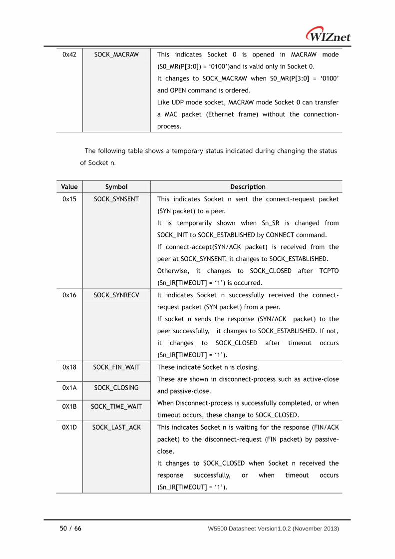
0x42 SOCK_MACRAW This indicates Socket 0 is opened in MACRAW mode
(S0_MR(P[3:0]) = ‘0100’)and is valid only in Socket 0.
It changes to SOCK_MACRAW when S0_MR(P[3:0] = ‘0100’
and OPEN command is ordered.
Like UDP mode socket, MACRAW mode Socket 0 can transfer
a MAC packet (Ethernet frame) without the connection-
process.
The following table shows a temporary status indicated during changing the status
of Socket n.
Value Symbol Description
0x15 SOCK_SYNSENT This indicates Socket n sent the connect-request packet
(SYN packet) to a peer.
It is temporarily shown when Sn_SR is changed from
SOCK_INIT to SOCK_ESTABLISHED by CONNECT command.
If connect-accept(SYN/ACK packet) is received from the
peer at SOCK_SYNSENT, it changes to SOCK_ESTABLISHED.
Otherwise, it changes to SOCK_CLOSED after TCPTO
(Sn_IR[TIMEOUT] = ‘1’) is occurred.
0x16 SOCK_SYNRECV It indicates Socket n successfully received the connect-
request packet (SYN packet) from a peer.
If socket n sends the response (SYN/ACK packet) to the
peer successfully, it changes to SOCK_ESTABLISHED. If not,
it changes to SOCK_CLOSED after timeout occurs
(Sn_IR[TIMEOUT] = ‘1’).
0x18 SOCK_FIN_WAIT These indicate Socket n is closing.
These are shown in disconnect-process such as active-close
and passive-close.
When Disconnect-process is successfully completed, or when
timeout occurs, these change to SOCK_CLOSED.
0x1A SOCK_CLOSING
0X1B SOCK_TIME_WAIT
0X1D SOCK_LAST_ACK This indicates Socket n is waiting for the response (FIN/ACK
packet) to the disconnect-request (FIN packet) by passive-
close.
It changes to SOCK_CLOSED when Socket n received the
response successfully, or when timeout occurs
(Sn_IR[TIMEOUT] = ‘1’).

W5500 Datasheet Version1.0.2 (November 2013) 51 / 66
Sn_PORT (Socket n Source Port Register) [R/W] [0x0004-0x0005] [0x0000]
Sn_PORT configures the source port number of Socket n. It is valid when Socket n
is used in TCP/UDP mode. It should be set before OPEN command is ordered.
Ex) In case of Socket 0 Port = 5000(0x1388), configure as below,
0x0004 0x0005
0x13 0x88
Sn_DHAR (Socket n Destination Hardware Address Register)
[R/W] [0x0006-0x000B] [0xFFFFFFFFFFFF]
Sn_DHAR configures the destination hardware address of Socket n when using
SEND_MAC command in UDP mode or it indicates that it is acquired in ARP-process by
CONNECT/SEND command.
Ex) In case of Socket 0 Destination Hardware address = 08.DC.00.01.02.10, configure as
below.
0x0006 0x0007 0x0008 0x0009 0x000A 0x000B
0x08 0xDC 0x00 0x01 0x02 0x0A

52 / 66 W5500 Datasheet Version1.0.2 (November 2013)
Sn_DIPR (Socket n Destination IP Address Register)
[R/W] [0x000C-0x000F] [0x00000000]
Sn_DIPR configures or indicates the destination IP address of Socket n. It is valid
when Socket n is used in TCP/UDP mode.
In TCP client mode, it configures an IP address of ‘TCP server’ before CONNECT
command.
In TCP server mode, it indicates an IP address of ‘TCP client’ after successfully
establishing connection.
In UDP mode, it configures an IP address of peer to be received the UDP packet by
SEND or SEND_MAC command.
Ex) In case of Socket 0 Destination IP address = 192.168.0.11, configure as below.
0x000C 0x000D 0x000E 0x000F
192 (0xC0) 168 (0xA8) 0 (0x00) 11 (0x0B)
Sn_DPORT (Socket n Destination Port Register) [R/W] [0x0010-0x0011] [0x00]
Sn_DPORT configures or indicates the destination port number of Socket n. It is
valid when Socket n is used in TCP/UDP mode.
In TCP client mode, it configures the listen port number of ‘TCP server’ before
CONNECT command.
In TCP server mode, it indicates the port number of ‘TCP client’ after successfully
establishing connection.
In UDP mode, it configures the port number of peer to be transmitted the UDP
packet by SEND/SEND_MAC command.
Ex) In case of Socket 0 Destination Port = 5000(0x1388), configure as below,
0x0010 0x0011
0x13 0x88

W5500 Datasheet Version1.0.2 (November 2013) 53 / 66
Sn_MSSR (Socket n Maximum Segment Size Register) [R/W] [0x0012-0x0013] [0x0000]
Sn_MSSR configures or indicates the MTU(Maximum Transfer Unit) of Socket n.
The default MTU is valid when Socket n is used in TCP / UDP mode. However, when
in PPPoE mode(MR[PPPoE] = ‘1’), it is determined within PPPoE MTU.
Mode Normal (MR(PPPoE)=‘0’) PPPoE (MR(PPPoE)=‘1’)
Default MTU Range Default MTU Range
TCP 1460 1 ~ 1460 1452 1 ~ 1452
UDP 1472 1 ~ 1472 1464 1 ~ 1464
MACRAW 1514
When Socket n is used in MACRAW mode, the default MTU is applied because the
MTU is not processed internally. Therefore, when transmitting the data bigger than
default MTU, the host should manually divide the data into the unit of default MTU.
When Socket n is used in TCP/UDP mode, and transmitting data bigger than MTU,
the data is automatically divided into the unit of MTU.
In UDP mode, because there is no such connection-process like in TCP mode, the
configured MTU is used. When transmitting data to a peer with the different MTU
size, the ICMP(Fragment MTU) packet might be received. In this case, IR(FMTU)
becomes ‘1’ and the peer information such as the MTU size and IP address is
indicated from FMTUR and UIPR respectively. If IR[MTU] = ‘1’, user cannot transmit
data to the peer. To resume the communication with peer, do as followed.
1. Close the Socket n by CLOSE command.
2. Set Sn_MSS to the indicated MTU from FMTUR
3. Open the Socket n by OPEN command
4. Resume the communication with the peer.
Ex) In case of Socket 0 MSS = 1460 (0x05B4), configure as below,
0x0012 0x0013
0x05 0xB4
Sn_TOS (Socket n IP Type of Service Register) [R/W] [0x0015] [0x00]
Sn_TOS configures the TOS(Type Of Service field in IP Header) of Socket n.
It is set before OPEN command.
For more the details, refer to http://www.iana.org/assignments/ip-parameters.
54 / 66 W5500 Datasheet Version1.0.2 (November 2013)
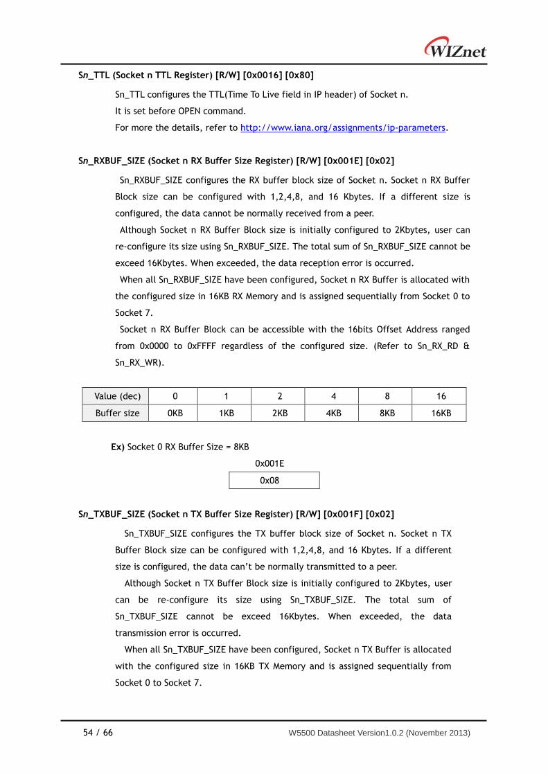
Sn_TTL (Socket n TTL Register) [R/W] [0x0016] [0x80]
Sn_TTL configures the TTL(Time To Live field in IP header) of Socket n.
It is set before OPEN command.
For more the details, refer to http://www.iana.org/assignments/ip-parameters.
Sn_RXBUF_SIZE (Socket n RX Buffer Size Register) [R/W] [0x001E] [0x02]
Sn_RXBUF_SIZE configures the RX buffer block size of Socket n. Socket n RX Buffer
Block size can be configured with 1,2,4,8, and 16 Kbytes. If a different size is
configured, the data cannot be normally received from a peer.
Although Socket n RX Buffer Block size is initially configured to 2Kbytes, user can
re-configure its size using Sn_RXBUF_SIZE. The total sum of Sn_RXBUF_SIZE cannot be
exceed 16Kbytes. When exceeded, the data reception error is occurred.
When all Sn_RXBUF_SIZE have been configured, Socket n RX Buffer is allocated with
the configured size in 16KB RX Memory and is assigned sequentially from Socket 0 to
Socket 7.
Socket n RX Buffer Block can be accessible with the 16bits Offset Address ranged
from 0x0000 to 0xFFFF regardless of the configured size. (Refer to Sn_RX_RD &
Sn_RX_WR).
Value (dec) 0 1 2 4 8 16
Buffer size 0KB 1KB 2KB 4KB 8KB 16KB
Ex) Socket 0 RX Buffer Size = 8KB
0x001E
0x08
Sn_TXBUF_SIZE (Socket n TX Buffer Size Register) [R/W] [0x001F] [0x02]
Sn_TXBUF_SIZE configures the TX buffer block size of Socket n. Socket n TX
Buffer Block size can be configured with 1,2,4,8, and 16 Kbytes. If a different
size is configured, the data can’t be normally transmitted to a peer.
Although Socket n TX Buffer Block size is initially configured to 2Kbytes, user
can be re-configure its size using Sn_TXBUF_SIZE. The total sum of
Sn_TXBUF_SIZE cannot be exceed 16Kbytes. When exceeded, the data
transmission error is occurred.
When all Sn_TXBUF_SIZE have been configured, Socket n TX Buffer is allocated
with the configured size in 16KB TX Memory and is assigned sequentially from
Socket 0 to Socket 7.
W5500 Datasheet Version1.0.2 (November 2013) 55 / 66
Socket n TX Buffer Block can be accessible with 16bits Offset Address ranged
from 0x0000 to 0xFFFF regardless of the configured size. (Refer to Sn_TX_WR &
Sn_TX_RD).
Value (dec) 0 1 2 4 8 16
Buffer size 0KB 1KB 2KB 4KB 8KB 16KB
Ex) Socket 0 TX Buffer Size = 4KB
0x001F
0x04
Sn_TX_FSR (Socket n TX Free Size Register) [R] [0x0020-0x0021] [0x0800]
Sn_TX_FSR indicates the free size of Socket n TX Buffer Block. It is initialized to
the configured size by Sn_TXBUF_SIZE. Data bigger than Sn_TX_FSR should not be
saved in the Socket n TX Buffer because the bigger data overwrites the previous
saved data not yet sent. Therefore, check before saving the data to the Socket n TX
Buffer, and if data is equal or smaller than its checked size, transmit the data with
SEND/SEND_MAC command after saving the data in Socket n TX buffer. But, if data is
bigger than its checked size, transmit the data after dividing into the checked size
and saving in the Socket n TX buffer.
If Sn_MR(P[3:0]) is not TCP mode(‘0001’), it is automatically calculated as the
difference between ‘Socket n TX Write Pointer (Sn_TX_WR)’ and ‘Socket n TX Read
Pointer (Sn_TX_RD)’.
If Sn_MR(P[3:0]) is TCP mode(‘0001’), it is automatically calculated as the
difference between Sn_TX_WR and the internal ACK pointer which indicates the
point of data is received already by the connected peer.
Ex) In case of 2048(0x0800) in S0_TX_FSR,
0x0020 0x0021
0x08 0x00
Sn_TX_RD (Socket n TX Read Pointer Register) [R] [0x0022-0x0023] [0x0000]
Sn_TX_RD is initialized by OPEN command. However, if Sn_MR(P[3:0]) is TCP
mode(‘0001’), it is re-initialized while connecting with TCP.
After its initialization, it is auto-increased by SEND command. SEND command
transmits the saved data from the current Sn_TX_RD to the Sn_TX_WR in the Socket
n TX Buffer. After transmitting the saved data, the SEND command increases the
Sn_TX_RD as same as the Sn_TX_WR. If its increment value exceeds the maximum

56 / 66 W5500 Datasheet Version1.0.2 (November 2013)
value 0xFFFF, (greater than 0x10000 and the carry bit occurs), then the carry bit is
ignored and will automatically update with the lower 16bits value.
Sn_TX_WR (Socket n TX Write Pointer Register) [R/W] [0x0024-0x0025] [0x0000]
Sn_TX_WR is initialized by OPEN command. However, if Sn_MR(P[3:0]) is TCP
mode(‘0001’), it is re-initialized while connecting with TCP.
It should be read or to be updated like as follows.
1. Read the starting address for saving the transmitting data.
2. Save the transmitting data from the starting address of Socket n TX
buffer.
3. After saving the transmitting data, update Sn_TX_WR to the
increased value as many as transmitting data size. If the increment
value exceeds the maximum value 0xFFFF(greater than 0x10000 and the
carry bit occurs), then the carry bit is ignored and will automatically
update with the lower 16bits value.
4. Transmit the saved data in Socket n TX Buffer by using SEND/SEND
command
Sn_RX_RSR (Socket n Received Size Register) [R] [0x0026-0x0027] [0x0000]
Sn_RX_RSR indicates the data size received and saved in Socket n RX Buffer.
Sn_RX_RSR does not exceed the Sn_RXBUF_SIZE and is calculated as the difference
between ‘Socket n RX Write Pointer (Sn_RX_WR)’ and ‘Socket n RX Read Pointer
(Sn_RX_RD)’.
Ex) In case of 2048(0x0800) in S0_RX_RSR,
0x0026 0x0027
0x08 0x00
Sn_RX_RD (Socket n RX Read Data Pointer Register) [R/W] [0x0028-0x0029] [0x0000]
Sn_RX_RD is initialized by OPEN command. Make sure to be read or updated as
follows.
1. Read the starting save address of the received data
2. Read data from the starting address of Socket n RX Buffer.
3. After reading the received data, Update Sn_RX_RD to the increased value as
many as the reading size. If the increment value exceeds the maximum value
0xFFFF, that is, is greater than 0x10000 and the carry bit occurs, update with
the lower 16bits value ignored the carry bit.
4. Order RECV command is for notifying the updated Sn_RX_RD to W5500.
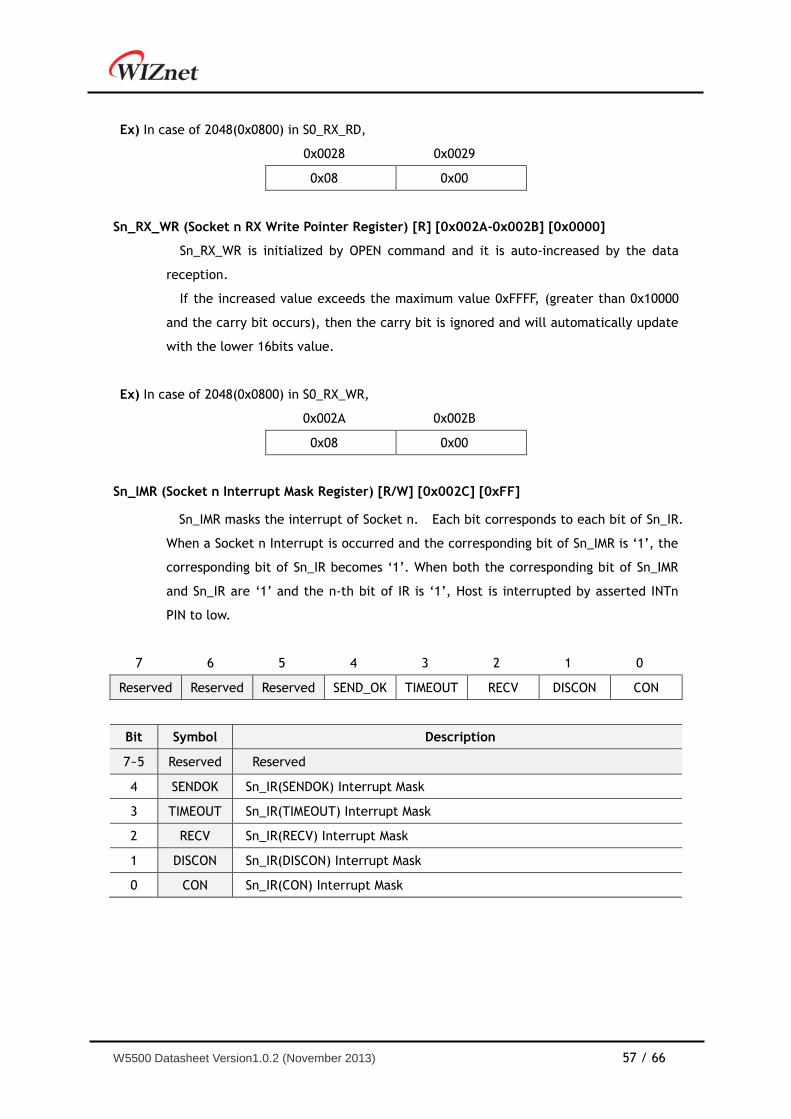
W5500 Datasheet Version1.0.2 (November 2013) 57 / 66
Ex) In case of 2048(0x0800) in S0_RX_RD,
0x0028 0x0029
0x08 0x00
Sn_RX_WR (Socket n RX Write Pointer Register) [R] [0x002A-0x002B] [0x0000]
Sn_RX_WR is initialized by OPEN command and it is auto-increased by the data
reception.
If the increased value exceeds the maximum value 0xFFFF, (greater than 0x10000
and the carry bit occurs), then the carry bit is ignored and will automatically update
with the lower 16bits value.
Ex) In case of 2048(0x0800) in S0_RX_WR,
0x002A 0x002B
0x08 0x00
Sn_IMR (Socket n Interrupt Mask Register) [R/W] [0x002C] [0xFF]
Sn_IMR masks the interrupt of Socket n. Each bit corresponds to each bit of Sn_IR.
When a Socket n Interrupt is occurred and the corresponding bit of Sn_IMR is ‘1’, the
corresponding bit of Sn_IR becomes ‘1’. When both the corresponding bit of Sn_IMR
and Sn_IR are ‘1’ and the n-th bit of IR is ‘1’, Host is interrupted by asserted INTn
PIN to low.
7 6 5 4 3 2 1 0
Reserved Reserved Reserved SEND_OK TIMEOUT RECV DISCON CON
Bit Symbol Description
7~5 Reserved Reserved
4 SENDOK Sn_IR(SENDOK) Interrupt Mask
3 TIMEOUT Sn_IR(TIMEOUT) Interrupt Mask
2 RECV Sn_IR(RECV) Interrupt Mask
1 DISCON Sn_IR(DISCON) Interrupt Mask
0 CON Sn_IR(CON) Interrupt Mask
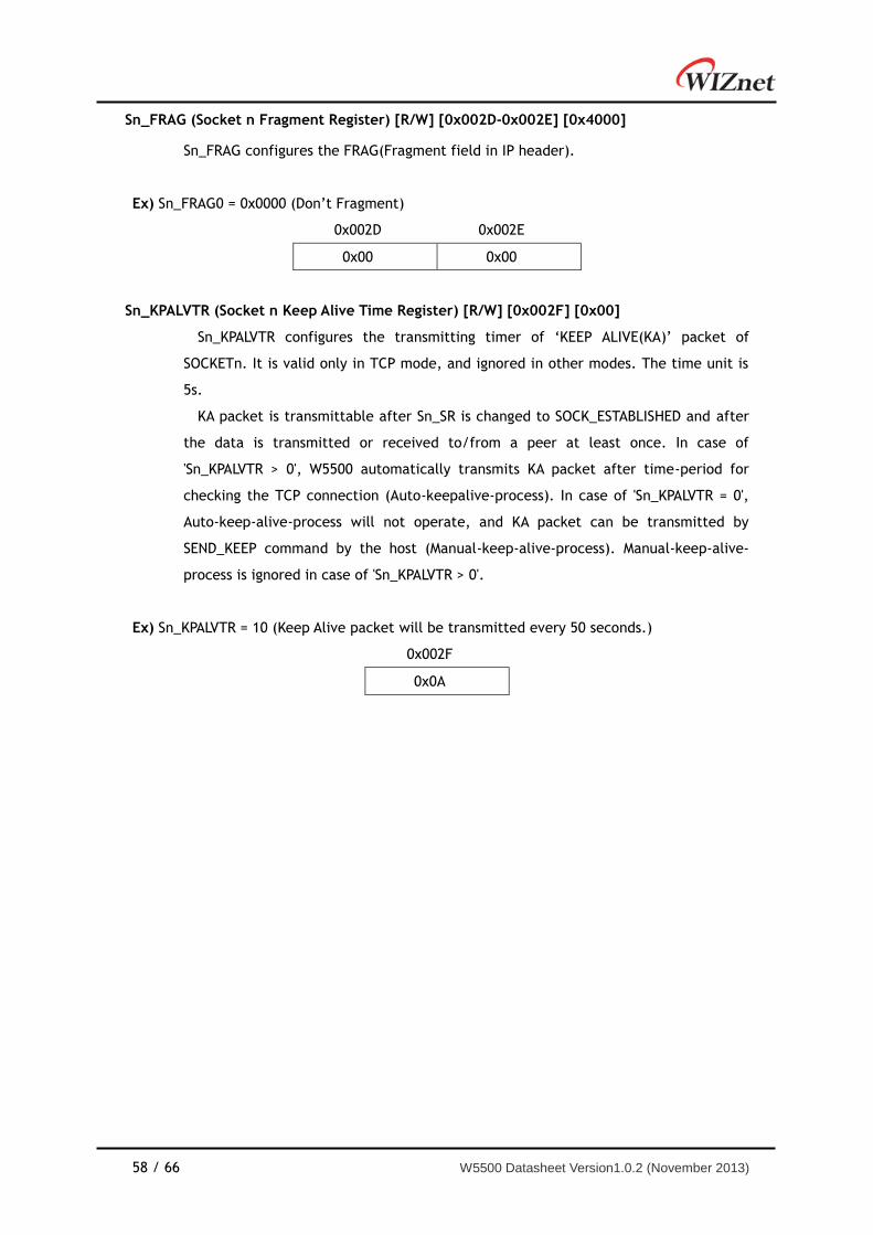
58 / 66 W5500 Datasheet Version1.0.2 (November 2013)
Sn_FRAG (Socket n Fragment Register) [R/W] [0x002D-0x002E] [0x4000]
Sn_FRAG configures the FRAG(Fragment field in IP header).
Ex) Sn_FRAG0 = 0x0000 (Don’t Fragment)
0x002D 0x002E
0x00 0x00
Sn_KPALVTR (Socket n Keep Alive Time Register) [R/W] [0x002F] [0x00]
Sn_KPALVTR configures the transmitting timer of ‘KEEP ALIVE(KA)’ packet of
SOCKETn. It is valid only in TCP mode, and ignored in other modes. The time unit is
5s.
KA packet is transmittable after Sn_SR is changed to SOCK_ESTABLISHED and after
the data is transmitted or received to/from a peer at least once. In case of
'Sn_KPALVTR > 0', W5500 automatically transmits KA packet after time-period for
checking the TCP connection (Auto-keepalive-process). In case of 'Sn_KPALVTR = 0',
Auto-keep-alive-process will not operate, and KA packet can be transmitted by
SEND_KEEP command by the host (Manual-keep-alive-process). Manual-keep-alive-
process is ignored in case of 'Sn_KPALVTR > 0'.
Ex) Sn_KPALVTR = 10 (Keep Alive packet will be transmitted every 50 seconds.)
0x002F
0x0A
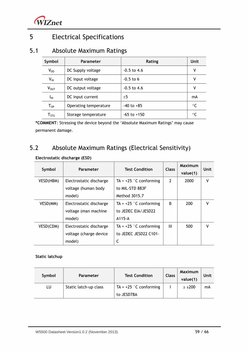
W5500 Datasheet Version1.0.2 (November 2013) 59 / 66
Electrical Specifications 5
5.1 Absolute Maximum Ratings
Symbol Parameter Rating Unit
VDD DC Supply voltage -0.5 to 4.6 V
VIN DC input voltage -0.5 to 6 V
VOUT DC output voltage -0.5 to 4.6 V
IIN DC input current 5 mA
TOP Operating temperature -40 to +85 C
TSTG Storage temperature -65 to +150 C
*COMMENT: Stressing the device beyond the ‘Absolute Maximum Ratings’ may cause
permanent damage.
5.2 Absolute Maximum Ratings (Electrical Sensitivity)
Electrostatic discharge (ESD)
Symbol Parameter Test Condition Class Maximum
value(1) Unit
VESD(HBM) Electrostatic discharge
voltage (human body
model)
TA = +25 °C conforming
to MIL-STD 883F
Method 3015.7
2 2000 V
VESD(MM) Electrostatic discharge
voltage (man machine
model)
TA = +25 °C conforming
to JEDEC EIA/JESD22
A115-A
B 200 V
VESD(CDM) Electrostatic discharge
voltage (charge device
model)
TA = +25 °C conforming
to JEDEC JESD22 C101-
C
III 500 V
Static latchup
Symbol Parameter Test Condition Class Maximum
value(1) Unit
LU Static latch-up class TA = +25 °C conforming
to JESD78A
I ≥ ±200 mA

60 / 66 W5500 Datasheet Version1.0.2 (November 2013)
5.3 DC Characteristics
(Test Condition: Ta = –40 to 85°C)
Symbol Parameter Test Condition Min Typ Max Unit
VDD Supply voltage Apply VDD, AVDD 2.97 3.3 3.63 V
VIH High level input
voltage
2.0 5.5 V
VIL Low level input
voltage
- 0.3 0.8 V
VT Threshold point All inputs except XI 1.30 1.41 1.53 V
VT+ Schmitt trig Low to
High Threshold point
All inputs except XI 1.53 1.64 1.73 V
VT- Schmitt trig High to
Low Threshold point
All inputs except XI 0.95 1.02 1.09 V
TJ Junction
temperature
0 25 125 °C
IL Input Leakage
Current
1 A
RPU Pull-up Resistor SCSn, RSTn, PMODE[2:0] 62 77 112 Kohm
RPD Pull-down Resistor RSVD(Pin 23, Pin 38 ~ Pin
42)
48 85 174 Kohm
VOL Low level output
voltage
IOL = 8mA,
All outputs except XO
0.4 V
VOH High level output
voltage
IOH = 8mA,
All outputs except XO
2.4 V
IOL Low level output
Current
VOL = 0.4V, All outputs
except XO
8.6 13.9 18.9 mA
IOH High level output
Current
VOH = 2.4V, All outputs
except XO
12.5 26.9 47.1 mA
IDD1 Supply Current
(Normal operation
mode)
VDD=3.3V, AVDD=3.3V, Ta
= 25°C
132 mA
IDD2 Supply Current
(Power Down mode)
PHY Power Down mode,
VDD=3.3V, AVDD=3.3V, Ta
= 25°C
13 mA

W5500 Datasheet Version1.0.2 (November 2013) 61 / 66
5.4 Power Dissipation
(Test Condition: VDD=3.3V, AVDD=3.3V, Ta = 25°C)
Condition Min Typ Max Unit
100M Link - 128 - mA
10M Link - 75 - mA
Un-Link (Auto-negotiation mode) - 65 - mA
100M Transmitting - 132 - mA
10M Transmitting - 79 - mA
Power Down mode - 13 - mA
5.5 AC Characteristics
5.5.1 Reset Timing
Figure 22. Reset Timing
Symbol Description Min Max
TRC Reset Cycle Time 500 us -
TPL RSTn to internal PLOCK (PLL Lock) - 1 ms
5.5.2 Wake up Time
Voltage Regulator Wake up Time: 10us
5.5.3 Crystal Characteristics
Parameter Range
Frequency 25 MHz
Frequency Tolerance (at 25) ±30 ppm
Shunt Capacitance 7pF Max
Drive Level 59.12uW/MHz
Load Capacitance 18pF
Aging (at 25) ±3ppm / year Max
RSTnTPL
TRC
PLOCK
(Internal)

62 / 66 W5500 Datasheet Version1.0.2 (November 2013)
5.5.4 SPI Timing
Figure 23. SPI Timing
4 Theoretical Guaranteed Speed
Even though theoretical design speed is 80MHz, the signal in the high speed may be distorted because
of the circuit crosstalk and the length of the signal line. The minimum guaranteed speed of the SCLK
is 33.3 MHz which was tested and measured with the stable waveform.
Please refer to the SPI Application Note which shows the WIZnet test environment and results.
5 2.1ns is when pn loaded with 30pF. The time is shorter with lower capacitance.
SCSn
SCLK
MOSI
MISO
TWH TWL
HI-Z HI-Z
VIH
VIL
VIH
VIL
VIH
VIL
VOH
VOL
TDS TDH
TOH TCHZTOV
TCSS
TCS
TCSH
Symbol Description Min Max Units
FSCK SCK Clock Frequency 80/33.34 MHz
TWH SCK High Time 6 ns
TWL SCK Low Time 6 ns
TCS SCSn High Time 30 ns
TCSS SCSn Setup Time 5 - ns
TCSH SCSn Hold Time 5 ns
TDS Data In Setup Time 3 ns
TDH Data In Hold Time 3 ns
TOV Output Valid Time 5 ns
TOH Output Hold Time 0 ns
TCHZ SCSn High to Output Hi-Z 2.15 ns

W5500 Datasheet Version1.0.2 (November 2013) 63 / 66
5.5.5 Transformer Characteristics
Parameter Transmit End Receive End
Turn Ratio 1:1 1:1
Inductance 350 uH 350 uH
Figure 24. Transformer Type
5.5.6 MDIX
W5500 does not support auto-MDIX feature.
Thus, user should use straight-through cables to connect to other switches or routers and
crossover cables to connect to devices such as servers, workstations or another W5500.
However, user can use either type of cable to connect to other devices with auto-MDIX
enabled, and the interface automatically corrects for any incorrect cabling.
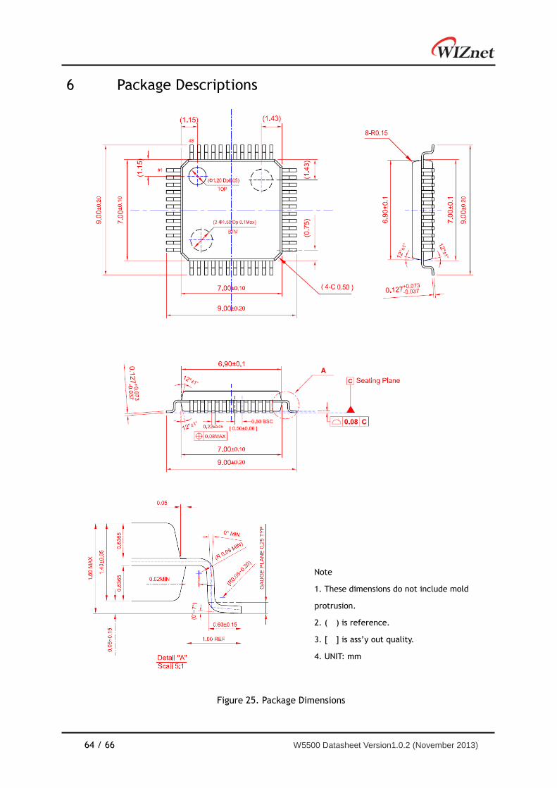
64 / 66 W5500 Datasheet Version1.0.2 (November 2013)
Package Descriptions 6
Figure 25. Package Dimensions
Note
1. These dimensions do not include mold
protrusion.
2. ( ) is reference.
3. [ ] is ass’y out quality.
4. UNIT: mm

W5500 Datasheet Version1.0.2 (November 2013) 65 / 66
Document History Information
Version Date Descriptions
Ver. 1.0.0 1AUG2013 Initial Release
Ver. 1.0.1 13SEP2013
Corrected duplicated statements and typing errors (P.14, 23, 24, 28,
39, 51)
Corrected descriptions (P.35)
Ver. 1.0.2 14NOV2013
1. Changed “descriptions of pin at 1.1 Pin Descriptions”(P.10)
from It must be tied to GND to NC(PIN38~42)
2. Corrected typing error :
from 0x02 to 0x42 value of SOCK_MACRAW at 4.2 Socket
Registers(P.50)

66 / 66 W5500 Datasheet Version1.0.2 (November 2013)
Copyright Notice Copyright 2013 WIZnet Co., Ltd. All Rights Reserved.
Technical Support: [email protected]
Sales & Distribution: [email protected]
For more information, visit our website at http://www.wiznet.co.kr