water-free dust removal for solar power plants … · web viewthe two-sided eds is fabricated on...
TRANSCRIPT
Water-Free Dust Removal for Solar Power Plants using R2R Flexographic Production of Electrodynamic Screens with Flexible Glass Encapsulation
Authors: Ryan Eriksen*1, Carolyn Ellinger2, Kevin O’Connor2, Doug Garman2, Sean Garner3, Annie Bernard1, Malay Mazumder1, Mark Horenstein1
Affiliations1 Boston University, Electrical and Computer Engineering Department, Boston MA2 Eastman Kodak Company, Rochester, NY3 Corning Research and Development Corporation, Corning NY
*Corresponding Author: Dr. Ryan EriksenBoston University, Electrical and Computer Engineering Department 8 Saint Marys Street, Room 324 Boston MA 02215Email: [email protected]: 617-353-2811Fax: 617-353-7337
AbstractNatural dust deposition, called soiling, plus the subsequent loss of output power due to the decrease in collected irradiance, is a significant challenge for solar power plant operators. The current industry standard is deluge washing, which can consume significant volumes of water and may limit the growth of solar power in arid climates if a water-free method of cleaning cannot be achieved. The Electrodynamic Screen (EDS) consists of rows of interdigitated electrodes that are installed on the optical surface of the solar collector. When the EDS electrodes are energized, an electric field is generated on the surface of the EDS, which charges, levitates, and then sweeps the dust particles away. Flexographic printing can achieve the high resolution and alignment needed for EDS production, and encapsulation using flexible glass allows for high environmental durability and the ability to retrofit existing solar collectors or photovoltaic panels. Cleaning with the EDS system has been shown to restore the output power of a photovoltaic panel to 97% of its original output, and to restore the specular reflectance of a solar mirror to 91% of its original output. This paper will summarize the current progress and challenges in EDS production and lamination in a roll-to-roll (R2R) process.
Introduction
Soiling With the increased deployment of photovoltaic (PV) and concentrated solar power (CSP), concern is growing over the sustainable growth of the industry, particularly in arid
1

climates. Arid regions are often ideal for solar power due to the high solar irradiance and low cloud cover, allowing for a plant to have a more consistent power output. However, these arid regions are often subject to dusty conditions. Dust will naturally deposit on the optical surface of the solar collectors, a process called soiling. The effect of soiling varies based upon the type of solar collector. Dust on PV panels will have a relatively small effect on the panel output, as a thin layer of dust will still scatter most light forward towards the collector. As a result, daily losses due to soiling for PV tends to only be between 0.5−1% per day. Soiling poses a much larger challenge for CSP. Even small angle scattering of the light in CSP can cause the light to fail to hit the collector, which can be hundreds of meters away in the case of concentrator towers. As a result, the average daily loss for CSP can range between 1−6%, depending upon the season [1]. For both types of solar power, these daily losses can quickly result in significant cumulative losses. These rates also exclude the instances of sporadic dust storms, which can cause a sudden and dramatic drop in power plant output [2].
The current industry standard for cleaning solar mirrors is deluge washing. This uses demineralized water, often mixed with detergents. Deluge washing has been shown to be the most effective method of cleaning, nearly completely restoring the optical surfaces to their clean state.
However, deluge washing has two major drawbacks. The first is that it disrupts normal plant operations. In CSP, mirrors must be angled down to allow the water and dust to drain. The second is that it uses large volumes of water, approximately 20−40 gallons of water per MWh generated per day [3]. For plants such as Crescent Dunes, which generate up to 110 MW, over ten thousand gallons of water may be used per day.
There are other methods that are less water intensive, such as brush cleaning that may be used for either CSP or PV. This method uses smaller volumes of water, but still suffers from the drawback of disrupting plant operations. In addition, brush cleaning is a more labor-intensive operation, and increases the risk of accidental damage to the collectors. Robotic cleaners are also being developed and can significantly reduce water consumption. However, these tend to have many moving parts, so their durability in the field is yet to be determined. Last, these methods ultimately rely upon making mechanical contact with the optical surface, which could lead to abrasion of the surface over time, ultimately leading to a long-term decrease in the power plant’s performance.
The EDS The Electrodynamic Screen (EDS) is an alternative technology that can be used to maintain the output of solar plants. The EDS presented here consists of three sets of interdigitated, parallel electrodes encased in a dielectric. Each set of electrodes is called a single phase, and the width and separation of these electrodes can vary (Figure 1a). The EDS can be installed onto the optical surface of the collector, and when the electrodes are energized with high voltage, an electric field is generated on the surface. This electric field charges, and then levitates the dust particles. The exact voltage applied to the electrodes is a system variable; in the work reported here a peak voltage of 1.2 kV was
2
used. By alternating the voltage of the phases in the correct sequence, a traveling electric wave is created, which pushes the dust off the edge of the optical surface (Figure 1b).
Figure 1 – a) shows the typical layout of a three-phase EDS, and b) shows a schematic of the EDS operation.
The effectiveness of the dust removal is dependent in part upon the strength of the electric field. The electric field is in turn affected by the magnitude of the applied voltage as well as the geometry of the electrodes. In general, the closer and wider electrodes are, the stronger the field will likely be. However, higher electrode coverage also means a greater loss in light transmittance to the solar collectors. This is measured by the transmission efficiency (TE) in PV and specular reflectance (SR) in CSP. To design an EDS for dust removal for solar collectors, a high SR and TE must be balanced with a strong electric field. In practice, electrode widths ranging from 100−1000 µm have been used, with electrode spacing’s from 300−3000 µm. Finer electrodes increase TE and SR but increase printing difficulty. A break in the electrode would result in a loss of coverage of the electric field over the non-energized portion of the electrode, due to the discontinuity. Therefore, dust would not be removed from this area. Furthermore, dust moved from other parts of the EDS may collected over the broken electrode.
Design RequirementsOne of the most critical design requirements is the minimization of irradiance loss to the collector due to the EDS. The EDS is therefore constructed using transparent materials. The ideal electrode material for PV applications would also be a transparent material. However, for CSP, reflective electrodes are also viable, permitting that the reflected light beam remains specular. To achieve this, the electrode’s surface would have to be extraordinarily smooth, with roughness on the order of 200 nm, and made from a reflective material. Alternatively, a reflective coating could be applied to the electrodes. For both PV and CSP, to minimize the loss of light to the collector, it is desirable that the electrodes be made as fine as possible with the electrode separation as large as possible. This must be co-optimized as to not adversely affect the dust removal efficacy.
The surface dielectric must also meet several requirements. The electric field generated by the electrodes decays exponentially, requiring that the EDS electrodes be in close proximity to the dust. Therefore, the surface dielectric must be quite thin. It must also be a strong dielectric to withstand the high voltages necessary for the EDS’s function. Last, it must be durable and resistant to abrasion. The surface dielectric will be exposed to the
3

elements, including UV, moisture, and windblown dust. A breakdown in the dielectric, either electrically or mechanically could result in a shorting between the electrodes of the EDS, causing a failure in the EDS.
Finally, the EDS must be mass-producible. A typical solar field may contain over a million square meters of solar collectors [4]. Roll-to-roll (R2R) manufacturing is the most practical production method that can produce the EDS in the volume needed for this application.
Methodology/Fabrication
StructureThe original designs produced on a lab scale, approximately 12x12 cm, were done using photolithography or screen-printing. The electrodes were patterned or printed directly onto thick glass substrates and then Corning® Willow® Glass, and was laminated over the electrodes using 3M 8146 OCA, illustrated in Figure 2. Willow Glass has a high dielectric strength, is ultrathin, has high abrasion resistance, and is flexible, which allows easier lamination [5]. This makes it an ideal candidate for the top dielectric. However, the printing processes were not scalable, and in the case of screen-printing, very fine electrodes were difficult to achieve.
Figure 2 – Initial EDS were printed directly into rigid glass substrates for stability and ease of manufacturing.
Third Phase The addition of a third phase increases the dust removal efficacy but adds to the manufacturing difficulty. Two-phase electrode layouts are trivial, but result in an electric field that has minimal lateral directional force. Three-phase EDS has the advantage of adding a lateral force to the dust particles, which can be aligned in the downward direction of the solar collector to take advantage of gravity and thus to increase dust removal. However, all three sets of electrodes cannot be printed on a single layer without two electrodes crossing.
There are several possible methods of laying out the third phase, including using nonparallel electrode geometries. A different method that had been used was to print an insulating dielectric layer over a section of electrodes and to then create a crossover
4

connection to the third phase (Figure 3). The insulating dielectric would prevent shorting of the two phases. However, the alignment and quality of the dielectric coating of the crossover is critical, and a single short will cause the EDS to fail. As previously mentioned, spacing between the electrodes is typically less than 1 mm and can be as small as 500 µm. In addition, the insulating dielectric was a potential point of electrical breakdown, which could decease the EDS longevity.
Figure 3 – The crossover connection allowed for a third phase but the dielectric also resulted in an electrical weak point and increased manufacturing difficulty.
One solution to this challenge is to print the third phase of the EDS on a separate side of the substrate. This increases the distance of the electrodes to the dust, but allows for a much simpler manufacturing process, as all three sets of electrodes can be printed in the same production run.
R2R Flexographic Print and Plate ProcessThe current generation of the EDS film has been produced at Kodak using flexographic printing in combination with electroless copper plating. Flexographic printing can achieve much higher resolution than screen printing, allowing for electrode geometries that were not achievable previously. A simplified schematic of Kodak’s manufacturing process is shown in Figure 4. The process uses a flexographic printing process to pattern catalytic ink on both sides of a flexible substrate. After printing, the substrate is conveyed through a touchless plating line where electroless copper is deposited on the printed catalyst pattern. The deposited copper is treated in-line with an environmental passivation, protecting the micro-wires from corrosion, all without contacting a roller to minimize the risk of conveyance-related defect formation. The end of the manufacturing line is equipped with in-line inspection tools for both electrical and optical measurements, and protective liner is applied to the EDS film post-inspection.
5
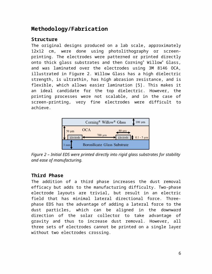
Figure 4 – Diagram illustrating Kodak’s print-and-plate process used to fabricate the EDS films.
Another innovation allowed by flexographic patterning was the use of a ladder structure for each electrode, as shown in Figure 5. While previous electrodes were solid, current EDS electrodes have an open area within the electrodes, allowing for light to pass through, while generating functionally similar electric fields to that of solid electrodes. This ultimately allowed for an improved TE and SR while maintaining similar electric field strength.
Figure 5 – Photomicrograph of flexographic patterned electrodes. Small defects such as the gap in one of the two rails in the lower left of the image have not been found to affect performance due to the ladder structure.
ResultsThe structure of the current generation EDS produced using Kodak’s manufacturing process is shown in Figure 6. The two-sided EDS is fabricated on PET (polyethylene terephthalate), which is laminated on top of the solar collector. A sheet of Willow Glass is then laminated onto the top surface as a protective layer and the top dielectric. Alternatively, the PET EDS film can be laminated onto Willow Glass, and the entire structure can then be laminated onto existing PV panels or solar mirrors using OCA. To
6

our knowledge, this is the first time that the EDS stack has been produced using exclusively R2R components and represents the one of first EDS systems to be commercially mass producible.
Figure 6 – Laminated structure of the current generation of the EDS device using flexographic printing.
The two-sided design has been shown to be significantly easier to manufacture than crossover designs. The change in the electric field caused by the increased distance between the electrodes and the dust was calculated to be a 12% decrease in the magnitude of the electric field. Using a slightly higher voltage on the bottom phase could easily compensate for this decrease; however, it did not produce a noticeable effect on the metrics used for dust removal. Figure 7 shows images before and after EDS activation.
Figure 7 − Left shows an EDS with dust deposited on the surface, before activation. Right shows the EDS after activation. The collected dust can be seen at the bottom of the image.
A range of electrode geometries is currently being investigated, with electrode widths ranging from 120 µm ladders to just 10 µm rails. The electrode spacing is also varied between 1400 and 700 µm. The electrode coverage ranges from 5.2% down to only 1% of the active area of the EDS.
To measure the efficacy of the EDS, two metrics were created: the Output Power Restoration (OPR) and Specular Reflectance Restoration (SRR). OPR is the ratio of the short-circuit current from a solar panel before and after EDS activation (equation 1),
7

while SRR is the ratio of the specular reflectance of the pristine mirror and the SR after EDS activation (equation 2):
OPR=I After Activation
I Clean (1) SRR=
SRAfter Activation
SRClean (2)
The power generated by a PV panel is proportional to the short-circuit current, thus OPR measures how much the EDS can restore a PV cell to the original clean. The SR is proportional to the output of a CSP plant, thus SRR is a measure used to determine the restoration of solar mirrors.
Flexographic printing also allows for larger EDS to be produced reliably. Previous work was focused on lab scale EDS, which were approximately 12 × 12 cm. Current designs are on a medium scale, which are approximately 30 × 30 cm.
Table 1 – Results of flexographic printed EDS produced by Eastman KodakOPR STD SRR STD
Lab Scale 96.8% 0.8 89.3% 1.6Med. Scale 94.5% 1.0 90.9% 2.8
Future WorkAll EDS stacks produced to date were assembled using manual lamination. R2R integration of the EDS with Willow Glass and OCA is still necessary for commercialization. Work is underway to locate integration partners for mass production.
Development is now underway to test the medium scale flexographic printed EDS laminated with Willow Glass in field trials. An automated setup is under construction and will be deployed in at least two arid climates in the following year: Sandia Desert in New Mexico, USA and the Atacama Desert in Chile.
Designs for a large-scale EDS are also underway, which would allow a tiled EDS to cover full-size PV panels or CSP mirrors. More work is underway to develop a process to retrofit the EDS device onto existing solar fields.
AcknowledgmentsWe acknowledge the grant from the Department of Energy (DOE CSP APOLLO EE-0007119) for supporting this research project on “Enhancement of Optical Efficiency of CSP Mirrors for Reducing O&M Cost via Near-Continuous Operation of Self-Cleaning Electrodynamic Screens (EDS)”. Support from MassCEC for a cost-sharing grant on the project is acknowledged. We are also grateful for the active partnership we receive from Corning Research and Development Corporation, Eastman Kodak Company, Sandia National Laboratory, and EDS Chile SpA.
8

References
1. T. Sarver, A. Al-Qaraghuli, L. Kazmerski, “A comprehensive review of the impact of dust on the use of solar energy: History, investigations, results, literature, and mitigation approaches”, Renewable and Sustainable Energy Reviews 22 (2013) 698–733.
2. Sayyah, M. N. Horenstein, M. K. Mazumder, “Energy yield loss caused by dust deposition on photovoltaic panels.” Solar Energy, vol. 107, p. 576−604, September 2014.
3. N. Bracken, et al., “Concentrating Solar Power and Water Issues in the U.S. Southwest”, Technical Report NREL/TP-6A50-61376, March 2015, The Joint Institute for Strategic Energy Analysis, https://www.nrel.gov/docs/fy15osti/61376.pdf
4. “Crescent Dunes.” Molten Salt Energy Storage - SolarReserve, SolarReserve, LLC., 18 May 2017, www.solarreserve.com/en/global-projects/csp/crescent-dunes.
5. Garner, S.M., Li, X., Huang, M-H. (2017) Introduction to Flexible Glass Substrates. In S.M. Garner (Ed.), Flexible Glass: Enabling Thin, Lightweight,and Flexible Electronics (pp.3-34). Hoboken, NJ: Wiley-Scrivener.
9