waveform generator implemented in fpga with an embedded ...19354/fulltext01.pdf · one alternative...
TRANSCRIPT

Waveform Generator Implemented in FPGA with an Embedded Processor
by
Anna Goman
LITH-ISY-EX-3412-2003
Linköping 2003


Waveform Generator Implemented in FPGA with an Embedded Processor
Master Thesis Division of Electronics Systems
Department of Electrical Engineering Linköping University, Sweden
Anna Goman LITH-ISY-EX-3412-2003
Handledare: Ulf Malmqvist och Magnus Johansson, Saab Bofors Dynamics
Examinator: Kent Palmkvist, ISY Linköpings Universitet Linköping 2003-08-29

Avdelning, Institution Division, Department
Institutionen för Systemteknik 581 83 LINKÖPING
Datum Date 2003-08-29
Språk Language
Rapporttyp Report category
ISBN
Svenska/Swedish X Engelska/English
Licentiatavhandling X Examensarbete
ISRN LITH-ISY-EX-3412-2003
C-uppsats D-uppsats
Serietitel och serienummer Title of series, numbering
ISSN
Övrig rapport ____
URL för elektronisk version http://www.ep.liu.se/exjobb/isy/2003/3412/
Titel Title
Implementering av vågformsgenerator i FPGA med inbyggd processor Waveform Generator Implemented in FPGA with an Embedded Processor
Författare Author
Anna Goman
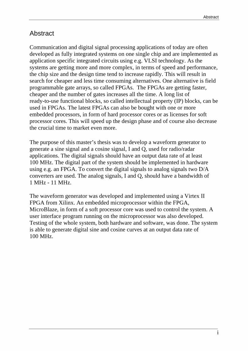
Sammanfattning Abstract Communication and digital signal processing applications of today are often developed as fully integrated systems on one single chip and are implemented as application specific integrated circuits using e.g. VLSI technology. As the systems are getting more and more complex in terms of speed and performance the chip size and the design time tend to increase rapidly. This will result in search for cheaper and less time consuming alternatives. One alternative is field programmable gate arrays, so called FPGAs. The FPGAs are getting faster, cheaper and the number of gates increases all the time. A long list of ready to use functional blocks so called intellectual property (IP) blocks can be used in FPGAs. The latest FPGAs can also be bought with one or more embedded processors, in form of hard processor cores or as licenses for soft processor cores. This will speed up the design phase and of course also decrease the crucial time to market even more. The purpose of this master’s thesis was to develop a waveform generator to generate a sine signal and a cosine signal, I and Q, used for radio/radar applications. The digital signals should have an output data rate of at least 100 MHz. The digital part of the system should be implemented in hardware using e.g. an FPGA. To convert the digital signals to analog signals two D/A converters are used. The analog signals, I and Q, should have a bandwidth of 1 MHz - 11 MHz. The waveform generator was developed and implemented using a Virtex II FPGA from Xilinx. An embedded microprocessor within the FPGA, MicroBlaze, in form of a soft processor core was used to control the system. A user interface program running on the microprocessor was also developed. Testing of the whole system, both hardware and software, was done. The system is able to generate digital sine and cosine curves of an output data rate of 100 MHz.
Nyckelord Keyword Waveform Generator, I/Q mixing, FPGA, Virtex, MicroBlaze, Embedded Development Kit, VHDL

Abstract
i
Abstract Communication and digital signal processing applications of today are often developed as fully integrated systems on one single chip and are implemented as application specific integrated circuits using e.g. VLSI technology. As the systems are getting more and more complex, in terms of speed and performance, the chip size and the design time tend to increase rapidly. This will result in search for cheaper and less time consuming alternatives. One alternative is field programmable gate arrays, so called FPGAs. The FPGAs are getting faster, cheaper and the number of gates increases all the time. A long list of ready-to-use functional blocks, so called intellectual property (IP) blocks, can be used in FPGAs. The latest FPGAs can also be bought with one or more embedded processors, in form of hard processor cores or as licenses for soft processor cores. This will speed up the design phase and of course also decrease the crucial time to market even more. The purpose of this master’s thesis was to develop a waveform generator to generate a sine signal and a cosine signal, I and Q, used for radio/radar applications. The digital signals should have an output data rate of at least 100 MHz. The digital part of the system should be implemented in hardware using e.g. an FPGA. To convert the digital signals to analog signals two D/A converters are used. The analog signals, I and Q, should have a bandwidth of 1 MHz - 11 MHz. The waveform generator was developed and implemented using a Virtex II FPGA from Xilinx. An embedded microprocessor within the FPGA, MicroBlaze, in form of a soft processor core was used to control the system. A user interface program running on the microprocessor was also developed. Testing of the whole system, both hardware and software, was done. The system is able to generate digital sine and cosine curves at an output data rate of 100 MHz.

Waveform Generator Implemented in FPGA with an Embedded Processor
ii
Acknowledgements
iii
Acknowledgements I would like to thank SAAB Bofors Dynamics in Linköping for letting me do my master’s thesis project at the company. I also would like to thank everyone at SBD that have helped and supported me during this time. I would like to give a special thanks to a few people at SBD and at the Division of Electronics Systems, Department of Electrical Engineering at Linköping University:
• My examiner Kent Palmkvist for introducing me to the area of FPGAs. • My supervisor Ulf Malmqvist at SBD for answering my questions and for
giving me an understanding of economical as well as technical aspects of a project in industry.
• My supervisor Magnus Johansson at SBD for all help with the technical issues, solving problems with the tools and answering questions.
• My family and my friends for the support during this time. • A big thank you to my boyfriend Niklas for all support and love during
this time.

Waveform Generator Implemented in FPGA with an Embedded Processor
iv

Abbreviations
v
Abbreviations ASIC Application Specific Integrated Circuit BMM Block RAM Memory Map BRAM Block Random Access Memory CDIP Custom Designed IP Block CLB Configurable Logic Block D/A Digital to Analog DAC D/A Converter DCM Digital Clock Management DSP Digital Signal Processing EDK Embedded Development Kit EDIF Electronic Design Interchange Format FDR Flip-flop of D-type with Reset signal FDRE Flip-flop of D-type with Reset and Enable signal FPGA Field Programmable Gate Array GUI Graphical User Interface I/O Input/Output IP Intellectual Property IPIF Intellectual Property InterFace JTAG Joint Test Action Group Libgen Library Generator LNA Low Noise Amplifier LMB Local Memory Bus LUT Look-Up Table LVDS Low Voltage Differential Signaling MHS Microprocessor Hardware Specification MPD Microprocessor Peripheral Description MSS Microprocessor Software Specification MVS Microprocessor Verification Specification OPB On-chip Peripheral Bus PAO Peripheral Analyze Order Platgen Platform Generator RISC Reduced Instruction Set Computer RF Radio Frequency SGP System Generator for Processors SoC System on Chip UART Universal Asynchronous Receiver/Transmitter VHDL VHSIC Hardware Description Language VHSIC Very High Speed Integrated Circuit VLSI Very Large Scale Integration XPS Xilinx Platform Studio

Waveform Generator Implemented in FPGA with an Embedded Processor
vi

Table of Contents
vii
Table of Contents 1 Introduction .......................................................................................1
1.1 Background................................................................................................ 1 1.2 Purpose ..................................................................................................... 2 1.3 Method....................................................................................................... 2 1.4 Reading Guidelines.................................................................................... 3
2 System Overview ..............................................................................5 2.1 Design and Implementation Alternatives.................................................... 6 2.2 Program Running on the Microprocessor .................................................. 7
3 Virtex II ..............................................................................................9 3.1 Virtex II FPGA............................................................................................ 9 3.2 The MicroBlaze Soft Core Processor....................................................... 11 3.3 On-Chip Peripheral Bus (OPB) ................................................................ 13
3.3.1 OPB Signals Naming Convention ...................................................................14 3.3.2 OPB Interface of CDIP ....................................................................................14 3.3.3 OPB Operations ..............................................................................................15 3.3.4 Bus Configuration............................................................................................17
4 Embedded Development Kit ...........................................................19 4.1 System Generator for Processors............................................................ 19 4.2 Xilinx Platform Studio............................................................................... 19
4.2.1 Creating a System...........................................................................................20 4.2.2 Adding Source Code .......................................................................................20 4.2.3 Software Flow..................................................................................................20 4.2.4 Hardware Flow ................................................................................................21 4.2.5 Memory Organization ......................................................................................21 4.2.6 Custom Designed IP blocks ............................................................................22 4.2.7 Implementation and Download........................................................................24
5 Peripherals and IP Blocks ...............................................................25 5.1 Universal Asynchronous Receiver/Transmitter ........................................ 25 5.2 Block RAM ............................................................................................... 26
5.2.1 Dual Port BRAM ..............................................................................................27 5.3 The Custom Designed IP Block, CDIP..................................................... 27
5.3.1 Peripheral Select, Pselect ...............................................................................30 5.3.2 Core.................................................................................................................31 5.3.3 Control and Status Register ............................................................................32
6 Implementation and Results............................................................35 6.1 Tools ........................................................................................................ 35 6.2 Source Code............................................................................................ 35
6.2.1 Special Instructions and Data Types for MicroBlaze.......................................35 6.2.2 Source Code ...................................................................................................36
6.3 P160 Analog Module................................................................................ 37 6.4 Difficulties ................................................................................................ 37
6.4.1 Difficulties with a Custom Designed IP Block ..................................................37 6.4.2 Endianness......................................................................................................38
6.5 Results..................................................................................................... 39 6.5.1 1 MHz Sine and Cosine Curves ......................................................................39 6.5.2 11 MHz Sine and Cosine Curves ....................................................................40 6.5.3 1 MHz to 10 MHz Sine and Cosine Curves .....................................................40

Waveform Generator Implemented in FPGA with an Embedded Processor
viii
7 Conclusion and Future Work...........................................................43 7.1 Conclusion ............................................................................................... 43 7.2 Future Work ............................................................................................. 43
8 References......................................................................................45 Appendix ................................................................................................49

List of Figures
ix
List of Figures Figure 1. I/Q Mixing in a Direct Conversion Receiver...............................1 Figure 2. The Waveform Generator .........................................................5 Figure 3. Characteristics of the User Interface Program ..........................7 Figure 4. Evaluation Board.......................................................................9 Figure 5. Virtex II Architecture Overview................................................10 Figure 6. Configurable Logic Block, CLB, of Virtex II .............................10 Figure 7. Slice Configuration of Virtex II .................................................11 Figure 8. MicroBlaze Core Block Diagram .............................................12 Figure 9. Pipeline Architecture ...............................................................12 Figure 10. Two Cycle Latency Due to Taken Branch.............................13 Figure 11. Delay Slots ............................................................................13 Figure 12. The Peripheral CDIP with OPB Interface ..............................14 Figure 13. Read Operation Over the OPB .............................................16 Figure 14. Write Operation Over the OPB..............................................16 Figure 15. Bus Configuration of MicroBlaze...........................................17 Figure 16. Xilinx Platform Studio ............................................................20 Figure 17. HW and SW Platform Generators .........................................21 Figure 18. Address Space Map..............................................................22 Figure 19. Hierarchy of a System...........................................................22 Figure 20. Hierarchy of myip .................................................................23 Figure 21. Transmitting of UART............................................................26 Figure 22. Receiving of UART................................................................26 Figure 23. ramb16_S9_S9 Component..................................................27 Figure 24. Components of the CDIP ......................................................28 Figure 25. FDR (a) and FDRE (b) Flip-flops...........................................30 Figure 26. The Core Component............................................................31 Figure 27. Send-Out Mode.....................................................................33 Figure 28. The System ...........................................................................34 Figure 29. P160 Analog Module.............................................................37 Figure 30. The Big Endian Bit Naming Convention of a Byte.................38 Figure 31. Sine and Cosine Curves of 1 MHz ........................................39 Figure 32. Sine and Cosine Curves of 11 MHz ......................................40 Figure 33. Sine and Cosine Curves Sweep from 1 MHz to 10 MHz.......41

Waveform Generator Implemented in FPGA with an Embedded Processor
x

List of Tables
xi
List of Tables Table 1. OPB Signals for CDIP…………………………...………………15 Table 2. Parameters of OPB UART Lite…………………………………25 Table 3. Generic Values for the CDIP……………………………………28 Table 4. Ports of the CDIP………………………………………………...29 Table 5. Generic Values and Ports of Pselect…………………………..31

Waveform Generator Implemented in FPGA with an Embedded Processor
xii

Chapter 1 Introduction
1
1 Introduction A lot of communication and digital signal processing (DSP) applications of today are developed as fully integrated systems on one single chip (System on Chip, SoC). In most cases the obvious choice of implementation for these dedicated applications would be an application specific integrated circuit (ASIC) using e.g. VLSI technology. The advantages of ASICs are the small chip size, the low power consumption and a very low cost per unit for large series [1]. As the systems are getting more and more complex in terms of speed and performance the chip size and, more importantly, the ASIC design time tend to increase rapidly. This will result in search for cheaper and less time consuming alternatives. One alternative could be programmable logic, especially field programmable gate arrays, so called FPGAs. The FPGA vendors claim that as FPGAs are getting faster, cheaper and the number of gates increases all the time, they will take the place of ASICs in the future [2]. The advantages of FPGAs are the possibility to reprogram the logic in case of errors in the design, faster prototyping that will lead to shorter design time and a lower cost per unit for small series. Most FPGA vendors provide a long list of ready-to-use functional blocks, so called intellectual property (IP) blocks. The latest FPGAs can also be bought with one or more embedded processors, in form of hard processor cores or as licenses for soft processor cores. This will speed up the design phase and of course also decrease the crucial time to market even more.
1.1 Background SAAB Bofors Dynamics AB is developing land, air and sea missile systems among other products [3]. In some of their products radio and radar technology is used.
Figure 1. I/Q Mixing in a Direct Conversion Receiver [4, p.19]
RF Filter
LP Filter
LP Filter LNA
Q = A cos w0t
I = A sin w0t
To DSP part
Antenna
A/D
A/D

Waveform Generator Implemented in FPGA with an Embedded Processor
2
In radio/radar applications it is common to use a technique with two sinusoidal signals with a phase shift of 90 degrees. The two signals, the in-phase signal (I) and the quadrature signal (Q) are used to mix another signal. Mixers or frequency converters convert a signal from one frequency, typically frf, to another frequency, typically fif [5]. Figure 1 shows an example of a direct conversion receiver part of a radio receiver where I/Q mixing is used.
1.2 Purpose Since SAAB Bofors Dynamics AB must put up a very high standard in terms of performance, safety and quality for their products they are often forced to use cutting edge technology. Therefore the company is always interested in using the latest technology. The purpose of this master’s thesis was to develop a waveform generator to generate the I and Q signals used for radio/radar applications described earlier. The digital signals should have an output data rate of at least 100 MHz, but the higher data rate the better. The analog sine curves should have a bandwidth of 1 MHz - 11 MHz. The system should be implemented in hardware using e.g. an FPGA. The two signals are generated from coefficients that are stored in RAMs. To control the waveform generator a control block should be developed. The control block can be designed as a microprocessor together with control logic and buses to transfer data.
1.3 Method The process to design the waveform generator started with a literature study of documentation on possible techniques to use and the available tools. After deciding on a suitable architecture for the system the design phase began. When a working design “in theory” was done the implementation phase started. The waveform generator was implemented in a Virtex II FPGA from Xilinx. An embedded microprocessor within the FPGA in form of a soft processor core was used. A user interface to operate the waveform generator in form of a program running on the microprocessor was then developed. Finally testing of the implemented waveform generator was done.

Chapter 1 Introduction
3
1.4 Reading Guidelines • Chapter 1. Introduction
The background, method and purpose of the master’s thesis are presented. • Chapter 2. System Overview
This chapter consists of an overview of the waveform generator. Design and implementation alternatives for the system and the user interface program are discussed.
• Chapter 3. Virtex II The Virtex II FPGA is described along with the MicroBlaze microprocessor and the bus OPB.
• Chapter 4. Embedded Development Kit The kit of hardware and software tools, EDK, is discussed.
• Chapter 5. Peripherals and IP Blocks All the peripherals connected to the OPB are presented. The custom designed IP block is also discussed in detail in this chapter.
• Chapter 6. Implementation and Results The implementation part is discussed and the results of the master’s thesis are presented. The implementation tools are presented along with the difficulties of the implementation part.
• Chapter 7. Conclusion and Future Work In this chapter conclusions about the project are made. Future work is also discussed.

Waveform Generator Implemented in FPGA with an Embedded Processor
4

Chapter 2 System Overview
5
2 System Overview The purpose of this master’s thesis project is to develop and implement a waveform generator generating two signals, a sine signal (I) and a cosine signal (Q). The two signals could be used in a radio/radar application like the one described in Section 1.1. The signals should be generated digitally, at an output data rate of at least 100 MHz, i.e. every 10 ns (or more often) new data is sent. The data comes from coefficients stored in two RAMs. A control block is used to control the RAMs. The control block is best designed as a microprocessor and control logic. The dashed part in figure 2 shows the digital part of the system. It should be implemented in hardware using e.g. an FPGA. The two generated digital signals are further connected to D/A converters to convert them into analog signals. The analog I and Q signals should have a bandwidth of 1 MHz - 11 MHz. To be able to operate the system a PC connected to an UART port is used (see figure 2). Via the PC it should be possible to load the RAMs with data, perform reads and writes to specific addresses and start the generation of the two signals. A user interface used to operate the waveform generator should also be developed.
Figure 2. The Waveform Generator
UART
RAM
Control Logic
I signal
Q signal
Microprocessor
RAM
DAC
LP
LP
DAC
12 bits out Analog signals

Waveform Generator Implemented in FPGA with an Embedded Processor
6
2.1 Design and Implementation Alternatives The waveform generator can be designed in many different ways. Choices concerning the system architecture and implementation have to be made in the beginning of the design phase. The control block is best designed in form of a microprocessor, control logic and buses to transfer data. The control block is then connected to the two RAMs. There are a number of ways on how the waveform generator could be implemented in hardware. The system could be designed with traditional electrical components e.g. a microprocessor, RAMs, multiplexers and DACs. This implementation alternative is not suitable, for this project, since the electrical components would take up a lot of space. The system could also be implemented as an ASIC on a chip. Since this alternative would be time-consuming and rather expensive it is not suitable for this project either. The fastest alternative is to implement the system using an FPGA. After this is decided there are still a few alternatives to consider when using an FPGA:
• Using an FPGA and develop the whole system using the hardware description language VHDL.
• Using an FPGA together with a microprocessor outside of the FPGA and develop the rest of the system using VHDL.
• Using an FPGA with an embedded microprocessor1 within the FPGA in form of a hard or soft processor core and develop the rest of the system using VHDL.
• Using an FPGA with an embedded microprocessor within the FPGA in form of a hard or soft processor core and using IP blocks to develop the rest of the system.
Due to the time limit of the master’s thesis project the alternative of using an FPGA with an embedded microprocessor and IP blocks is chosen. A Virtex II FPGA from Xilinx is chosen for implementation. The soft processor core MicroBlaze can be implemented in the Virtex II FPGA and it can be run at a maximum clock frequency of 150 MHz. This should be enough to reach the performance requirement of a minimum of 100 MHz output data rate for the digital I and Q signals.
1 In this document “embedded microprocessor” refers to a microprocessor that is instantiated in the FPGA as a hard or soft processor core. The microprocessor is possible to program by any user. It is not “embedded” in the way that it is hidden from the user.

Chapter 2 System Overview
7
2.2 Program Running on the Microprocessor It should be possible to operate the waveform generator via a PC. One should be able to load the RAMs with data, clear the RAMs, perform reads and writes to specific addresses and start the generation of the waveform signals. The user interface used to do this is developed as a program running on the microprocessor. A diagram of the characteristics of the user interface program is shown in figure 3. Since the waveform signals have a duration of 2048 (2 kB) samples it would be preferred if the loading of the RAMs is made from a data file.
Figure 3. Characteristics of the User Interface Program
What do you want to do?
What memory? Which file to load?
What memory? What address? What to write?
Load memory Write to address Read address
Send out waveform Clear memory Exit
What memory? What address?
Which byte?
What memory?
Memory is loaded
Reading is done
Writing is done
Clearing of memory is
done
Sending out of the waveform
Exiting the program
Start

Waveform Generator Implemented in FPGA with an Embedded Processor
8

Chapter 3 Virtex II
9
3 Virtex II The FPGA chosen for this project is the XC2V1000 with one million system gates, a Xilinx device from the Virtex II series. The FPGA is part of an evaluation board (see figure 4) together with a number of standard communication interfaces e.g. a JTAG port, a UART RS-232 port, LVDS ports and a P160 Expansion slot.
Figure 4. Evaluation Board [6, p. 1]
The evaluation board was bought together with the development tool Embedded Development Kit (EDK) from Xilinx. Up until the beginning of this master’s thesis these tools were rather new to Saab Bofors Dynamics AB and had never really been used before at the company. A large part of the project was spent on learning and evaluating the tools.
3.1 Virtex II FPGA Figure 5 shows the architecture overview of the Virtex II FPGA. The Virtex II device is a programmable gate array. It consists of arrays of configurable logic blocks (CLB) that are connected together to form combinatorial and synchronous logic. The CLBs can also be connected to large memory blocks (block RAMs) and multipliers (see figure 5). Programmable I/O blocks provide the interface between package pins and the internal configurable logic and digital clock manager (DCMs) blocks provide clock distribution delay compensation, clock multiplication and division and clock phase shifting [7].
UART RS-232 Port
DIP Switches
7-Segment Displays
Push Button Switches
P-160 Expansion Slot SelectMAP
ISP PROM
JTAG Port DDR Memory
Power Supplies
Vitex II FPGA LVDS
Receive Port LVDS
Transmit Port Dual Clock Oscillators

Waveform Generator Implemented in FPGA with an Embedded Processor
10
Figure 5. Virtex II Architecture Overview [7, p. 3] In figure 6 the structure of the CLB is presented. Each CLB consists of 4 slices (see figure 7). A slice includes two 4-input function generators, carry logic, arithmetic logic, multiplexers and two storage elements. The function generators are implemented as 4-input look-up tables (LUTs) and can be used to implement any boolean function of four inputs [8].
Figure 6. Configurable Logic Block, CLB, of Virtex II [8, p. 12]
Switch Matrix
Slice X0 Y0
Slice X0 Y1
Slice X1 Y0
Slice X1 Y1
Shift
CoutCin
Cout
Cin
Fast Connections to Neighbors
TBUF X0Y1 TBUF X0Y0
Programmable I/Os
Configurable Logic
DCM
CLB I/O Block RAM
Multiplier

Chapter 3 Virtex II
11
Figure 7. Slice Configuration of Virtex II [8, p. 12]
3.2 The MicroBlaze Soft Core Processor With a Virtex II device it is possible to use any soft embedded processor. As the EDK tool includes a license for the MicroBlaze soft processor core it was natural to use the MicroBlaze processor for this project. MicroBlaze is a 32-bit reduced instruction set computer (RISC) of Harvard architecture, i.e. with separate bus and memory for data and instructions respectively. The processor has thirty-two 32-bit general-purpose registers. The 32-bit data and instruction bus interface is suitable for IBM’s on-chip peripheral bus (OPB) that is described in Section 2.3. A fast local memory bus (LMB) can also be connected to the processor (see figure 8) [9]. At a maximum clock frequency of 150 MHz MicroBlaze can deliver 125 D-MIPS (Drystone, million instructions per second).
Register
LUT F
LUT G
Register
SRL 16
RAM 16
SRL 16
RAM 16
CY
CY
Arithmetic Logic
ORCY
MUXF5
MUXFx

Waveform Generator Implemented in FPGA with an Embedded Processor
12
Figure 8. MicroBlaze Core Block Diagram [9, p. 3] The processor has a three stages pipeline architecture to increase the speed. The completion of one instruction is divided into three stages: fetch, decode and execute. One instruction takes three cycles to be completed but three instructions can be done in parallel and all three pipeline stages are working at the same time (see figure 9) [9].
Figure 9. Pipeline Architecture [9, p. 8] The problem with pipelining is when the program takes branches. The two following instructions, already fetched and decoded, are wrong and have to be flushed from the pipeline when a branch is taken. The right instruction, the branch instruction target, cannot be started until the branch instruction is executed (see figure 10). This gives a latency of two cycles. To reduce this latency for taken branches MicroBlaze uses two techniques, the use of delay slots and the use of a history buffer [9]. The technique to use delay slots gives rise to only one cycle latency if a branch is taken. The idea is to rearrange the instructions of a program and allow the instruction following the branch instruction to finish (see figure 11). The branch is then delayed and a delay slot is produced. Since the instruction following the branch instruction is not to be flushed from the pipeline the performance is improved. This technique is only useful if there is a suitable instruction to put
Bus IF
Program Counter
Instruction
Buffer
ILMB Instruction
Decode
IOPB
Register File
32 x 32b
Add / Sub
Shift / Logical
Multiply
Bus IF
DLMB
DOPB
Fetch Decode Execute
Fetch Decode Execute Fetch Decode Execute
cycle 1 cycle 3 cycle 2 cycle 4 cycle 5 Instruction 1 Instruction 2 Instruction 3

Chapter 3 Virtex II
13
directly after the branch instruction. Otherwise a no-operation (NOP) has to be put there [9] [10].
Figure 10. Two Cycle Latency Due to Taken Branch
Figure 11. Delay Slots The second technique, to use a history buffer, is used on interrupts and exceptions. Old values from the register file are copied into the history buffer. On interrupt or exception the contents of the history buffer are copied back into the register file to restore the previous state [11].
3.3 On-Chip Peripheral Bus (OPB) A license for the on-chip peripheral bus (OPB) from IBM is included with the EDK tool. Since this bus is a suitable interface between MicroBlaze and different peripherals it was chosen to be a part of the system. With the OPB it is possible to have up to a 64-bit address bus and a 32 or 64-bit data bus. For this project both address and data buses were set to 32 bits. Peripherals of the bus can be implemented as 8, 16 or 32 bit slaves. 32 or 64 bit master peripherals are also supported. Some of the features of the fully synchronous bus are optional byte-enable support and dynamic bus sizing allowing byte, halfword, fullword and doubleword transfers [12].
Fetch Decode Execute
Fetch Decode Fetch
cycle 1 cycle 3 cycle 2 cycle 4 cycle 5 Branch Instruction
Instruction 2 Instruction 3
Branch Instruction Target Fetch Decode Execute
cycle 6
Fetch Decode Execute
Fetch Decode
cycle 1 cycle 3 cycle 2 cycle 4 cycle 5 Branch Instruction
Instruction 2 Branch Instruction Target Fetch Decode Execute
Execute

Waveform Generator Implemented in FPGA with an Embedded Processor
14
3.3.1 OPB Signals Naming Convention Peripherals connected to the OPB must use a certain naming convention. Signals that are outputs from the OPB and inputs to the slave must have names that start with OPB_. Signals that are inputs to the OPB and outputs from the slave must have names that start with Sln_. The outputs from the slave must be driven to logic ‘0’ when they are not used [12]. Peripherals, in form of IP blocks, are added to the system in the EDK (described in Chapter 4). The interface of each IP must be described in a microprocessor peripheral description file (MPD) for EDK to know how to connect each peripheral with the OPB. For every IP provided by Xilinx an MPD file is also provided but for a custom designed OPB slave an MPD file needs to be created. The file must follow a certain syntax described in [13]. The MPD file defines not only the OPB interface but also generic values and global ports such as clock and reset signals and external I/Os. The MPD file for the custom designed IP block (CDIP) for this project is included in Appendix. The CDIP is discussed in detail in Section 5.3.
3.3.2 OPB Interface of CDIP To be able to connect the CDIP to the OPB an OPB interface had to be defined. The OPB interface can be defined in a number of ways, from a very simple interface with only memory-mapped registers up to a complex interface with e.g. FIFOs, DMAs, interrupt control and master attachment. In the case with a complex interface the best idea is to use the intellectual property interface (IPIF) approach described in [14]. The IPIF is a parametric soft IP core provided by Xilinx [14]. The interface of CDIP is similar to a memory-mapped interface, so it could be made using a simple interface with only the most necessary signals. Which these signals are can be found in [14]. In table 1 the signals for the OPB interface of CDIP are listed. Figure 12 shows CDIP with its OPB interface.
Figure 12. The Peripheral CDIP with OPB Interface
CDIP
OPB_ABus OPB_BE OPB_Clk
OPB_DBus OPB_RNW OPB_Rst
OPB_select OPB_seqAdd
Sln_DBus Sln_errAck Sln_retry
Sln_toutSup Sln_xferAck
OPB

Chapter 3 Virtex II
15
Table 1. OPB Signals for CDIP [14, p. 4-7]
Signal Name Direction Width Description OPB_ABus Input [0:31] Address bus from OPB to slave. OPB_BE Input [0:4] Byte-enable signal. Indicates which
bytes are to be transferred. OPB_Clk Input 1 Clock signal. OPB_DBus Input [0:31] Data bus from OPB to slave. OPB_RNW Input 1 Read not write signal. Read when
‘1’, write when ‘0’. OPB_Rst Input 1 Reset signal. OPB_select Input 1 Select signal. Activated during
transfer. OPB_seqAddr Input 1 Sequential address signal.
Indicates that the following transfer will address the same slave.
Sln_DBus Output [0:31] Data bus from slave to OPB. Sln_errAck Output 1 Error acknowledgement signal.
Indicates error at transfer. Sln_retry Output 1 Retry signal. Indicates that transfer
cannot be performed at this time. Sln_toutSup Output 1 Time out suppression signal
indicates that transfer will be delayed. After 16 cycles a bus time out will occur. The signal is used to suppress a bus timeout and has to be asserted within 16 cycles from the activation of OPB_select.
Sln_xferAck Output 1 Transfer acknowledgement signal. Indicates that a transfer is completed. Is active (high) for one cycle at the end of the transfer.
3.3.3 OPB Operations The OPB interface of CDIP is mainly used to transfer data back and forth between MicroBlaze and CDIP. CDIP consists of RAM and the possible operations are writing to the memory and reading from the memory. There are also a few special operations that can be performed but they will be discussed later on. Figure 13 and figure 14 show read respectively write operation over the OPB.
• Read Operation: When OPB_select becomes active and the right address is sent on OPB_ABus the slave performs a read (if OPB_RNW is ‘1’) from the selected address of the memory. The slave puts the read data on Sln_DBus and sets Sln_xferAck active during the time data is valid on

Waveform Generator Implemented in FPGA with an Embedded Processor
16
Sln_DBus (one clock cycle). OPB_select becomes inactive when Sln_xferAck becomes inactive and the transfer is completed [12].
• Write Operation: When OPB_select becomes active and the right address
is sent on OPB_ABus the slave performs a write (if OPB_RNW is ‘0’) to the selected address of the memory. The slave puts the data from OPB_DBus into the memory on the selected address and sets Sln_xferAck active during one clock cycle when the data is written. OPB_select becomes inactive when Sln_xferAck becomes inactive and the transfer is completed [12].
Figure 13. Read Operation Over the OPB [12, p. 38]
Figure 14. Write Operation Over the OPB [12, p. 38]
Data
Address
OPB_Clk
OPB_select OPB_RNW
OPB_ABus
OPB_DBus
Sln_xferAck
Data
Address
OPB_Clk
OPB_select
OPB_RNW
OPB_ABus
Sln_DBus
Sln_xferAck

Chapter 3 Virtex II
17
3.3.4 Bus Configuration Since MicroBlaze is of Harvard architecture it has separate sides for instructions and data, both for the OPB and for the LMB. The sides are IOPB (instruction OPB), DOPB (data OPB), ILMB (instruction LMB) and DLMB (data LMB). Both, only one or none of the sides of each bus can be used. However the MicroBlaze bus interface is configurable in the following six ways [9]:
1. IOPB+DOPB+ILMB+DLMB 2. IOPB+DOPB+DLMB 3. DOPB+ILMB+DLMB 4. IOPB+DOPB+ILMB 5. IOPB+DOPB 6. DOPB+ILMB
Configuration 3 was chosen for this project (see figure 15) because fast internal instruction and data memory was wanted for this application. The DOPB can be used for peripherals such as UARTs, timers, general purpose I/O, additional BRAM and custom peripherals.
Figure 15. Bus Configuration of MicroBlaze [9, p. 17]
D/I BRAM
ILMB DLMB
DOPB
CDIP2 UART
CDIP1

Waveform Generator Implemented in FPGA with an Embedded Processor
18

Chapter 4 Embedded Development Kit
19
4 Embedded Development Kit The Embedded Development Kit (EDK) from Xilinx is used to design embedded programmable systems and it is a combination of hardware and software tools. The EDK supports design of processor sub-systems, e.g. the MicroBlaze soft processor core.
4.1 System Generator for Processors The tool System Generator for Processors (SGP) is a part of the EDK. With this tool the processor is selected and customized, buses and peripherals are customized and connected, and I/Os are set and connected to internal signals. All the steps are done graphically within the SGP graphical user interface (GUI). Besides from a library of provided IP blocks custom designed IP blocks can be added and used as peripherals. SGP can be used to create the whole system. The tool can generate netlists, simulation models and interfaces to the software application. It is also possible to only define the system in terms of processor, buses and peripherals and let SGP generate a microprocessor hardware specification (MHS) file. The MHS file is then used by Xilinx Platform Studio (XPS) for netlist generation, library generation etc. [15]. At the time of this project only a beta version of SGP was available, SGP 1.2 Beta, and the tool sometimes crashed without reason. Another problem was that it was difficult to do changes to a saved system, which made it necessary to create a new system every time. After studying how the SGP created the MHS it was decided that the design of the MHS file and the changes made to the MHS file should be done in a text editor instead of using the SGP tool. The MHS file for the system is included in Appendix.
4.2 Xilinx Platform Studio The Xilinx Platform Studio of the EDK Version 3.1.2 was used for this project. With this version of the tool it is possible to create a hardware platform in form of an MHS file, create a software platform, generate netlists and simulation models, debugging etc. [13].

Waveform Generator Implemented in FPGA with an Embedded Processor
20
4.2.1 Creating a System There are two ways to create a system using the XPS. The first one is to start with an empty MHS file and define processor, buses and peripherals with the “Add/Edit Cores... (dialog)” option in the “ Project” menu2. When creating the MHS file the microprocessor software specification (MSS) file and the microprocessor verification specification (MVS) file are created automatically. Changes can be made to the files afterwards using e.g. a text editor. The other way to create a system is to use an already made MHS file. The file can be made using SGP or a text editor. The MSS and MVS files are created automatically when a new system is created in the XPS.
4.2.2 Adding Source Code The program to be run on the processor can be coded in the language C or assembly. The source code is added to the XPS by right clicking on “Sources” in the tree-view in XPS. Source files (.c) and header files (.h) can be added. The source code for this system is discussed in Section 6.2.
4.2.3 Software Flow The software platform is generated by the library generator (Libgen). Its input is the MSS file, which defines e.g. driver and library customization parameters for peripherals and standard I/O devices (see right hand side of figure 17). Libgen also uses the MHS file as an input since the MSS file has a dependency on the MHS file. Libgen generates libraries and device drivers (libc.a, libXil.a,…) when the “Generate Libraries” button is clicked in the XPS (see figure 16).
Figure 16. Xilinx Platform Studio [16]
2 In the latest version of EDK, Version 3.2.2, the MHS file can be created using a graphical block diagram editor [17].

Chapter 4 Embedded Development Kit
21
The source code is compiled by the EDK using a GNU compiler when clicking on the “Compile Program Source” button in the XPS [13]. The compiler also uses the libraries generated by Libgen as input. The program source is transformed into bit patterns that are stored in the physical memory in the FPGA.
4.2.4 Hardware Flow The MHS file is used by the platform generator (Platgen) to generate the hardware in form of VHDL files and a netlist (EDIF) (see left hand side of figure 17) [13]. Platgen is activated when the button “Generate Netlist” is pressed in the XPS. To activate the implementation tool the “Generate Bitstream” button is used. In the block RAM memory map (BMM) file the memory space and the memory device organization is described.
Figure 17. HW and SW Platform Generators [13, p.22 and p. 24]
4.2.5 Memory Organization The memory space is divided into the system address space and the user address space (see figure 18). Since the address bus is 32 bits the total address space reaches from address 0 to address 0xFFFFFFFF (hexadecimal). In the first part the LMB memory space is situated. The OPB and each peripheral also have unique addressable memory space.
EDIF, VHD, BMM
MHS File MSS, MHS File
MSS File MHS File HW Specification
Editor
SW Platform Generator
SW Specification Editor
HW Platform Generator
XPS

Waveform Generator Implemented in FPGA with an Embedded Processor
22
Figure 18. Address Space Map [13, p. 256]
4.2.6 Custom Designed IP blocks In the case when a custom designed IP block is defined in the MHS file there are a few things one has to consider when using the XPS. To make the XPS be able to find the IP block a certain hierarchy of files has to be used. There are three places where the designed IP block can be placed [13]:
• In the directory that the environment variable XIL_MYPERIPHERALS is set to.
• In the directory that the system is created (see figure 19). • In the directory that the ”Peripheral Repository Directory” option in the
XPS is set to.
Figure 19. Hierarchy of a System
Empty Address Space
LMB Memory
OPB Memory
Address 0x0
Peripherals
Address 0xFFFFFFFF
system
data hdl myip code
vhdl

Chapter 4 Embedded Development Kit
23
The directory described above must contain a folder with the name myip where the design is placed. One or more custom designed IP blocks can be placed in this folder (see figure 20), each in a folder with the name of the IP block. The IP blocks can be of different versions. If versions are used, the name of the IP block must have the following syntax “name_of_ip_v1_00_a” if the version is 1.00.a. Without version the name is simply “name_of_ip”. If the MHS file is made using the SGP or the XPS, version is added automatically in the MHS file. This can be erased in a text editor if not wanted. Figure 20 shows the hierarchy of the myip folder. All the IP block folders in the myip folder must contain two folders, one data folder and one hdl folder. In the data folder the MPD file (described in Section 3.3.1) and the peripheral analyze order (PAO) file are placed. The PAO file contains a list of HDL files that are needed for synthesis, and defines the analyze order for compilation [13]. The MPD and PAO files must have version names and the version must be the same as the platform specification format, in this case 2.0.0. The hdl folder contains a folder named vhdl where the vhdl files for the IP block are placed (verilog files can be used instead of vhdl). The files for the CDIP, CDIP_v2_0_0.mpd and CDIP_v2_0_0.pao can be found in Appendix.
Figure 20. Hierarchy of myip
myip
ip1 ip2 ip3
MPD PAO
data hdl
vhdl
Waveform Generator Implemented in FPGA with an Embedded Processor
24
4.2.7 Implementation and Download As described earlier the XPS generates the hardware and the software platforms of the system. To merge the hardware and software together the “Update Bitstream” button is used. This invokes the tool data2bram that makes the hardware and the software flows come together. It also calls hardware and software flow tools if required. At the end of this stage the download.bit file is generated. It contains information regarding both the software and the hardware part of the design [13]. The download.bit file is downloaded to the FPGA with the “Download” button.

Chapter 5 Peripherals and IP Blocks
25
5 Peripherals and IP Blocks Peripherals are components connected to the OPB. They can be of slave or master type. MicroBlaze (described in Section 3.2) is a peripheral used as master of the OPB. The peripherals can also be used for e.g. different communication purposes, as memories or for digital signal processing. The FPGA vendors provide a number of peripherals in form of IP blocks.
5.1 Universal Asynchronous Receiver/Transmitter To be able to establish a communication between the FPGA and a PC a universal asynchronous receiver/transmitter (UART) can be used. The OPB UART Lite is a free of charge IP core provided by Xilinx [9]. The OPB UART Lite has two full duplex channels, receive (rx) and transmit (tx). The channels are connected to two global ports, RX and TX, which are connected to the UART RS-232 port on the evaluation board (see figure 4). A cable is connected between the UART RS-232 port on the evaluation board and a PC. More advanced UARTs, such as the OPB UART 16450 and OPB UART 16550, can be bought from Xilinx. The lighter version, OPB UART Lite (Version 1.00b), is however suitable for this project. The UART Lite supports an 8-bit bus interface and can be connected to the OPB directly. The UART Lite can be parameterized to fit a specific system. Some parameters that can be changed are clock frequency, baud rate, number of data bits and parity [9]. For this project the parameters in table 2 were chosen.
Table 2. Parameters of OPB UART Lite Parameter Name/Description Value
C_BASE_ADDR Base address 0xFFFF4100 C_HIGH_ADDR High address 0xFFFF41FF C_DATA_BITS Number of data bits 8 (5 to 8 possible) C_CLK_FREQ Clock frequency 24 MHz C_BAUDRATE Baud rate 19200 bits/second C_USE_PARITY Parity 0 (No parity) Data is transmitted serially with the LSB first using the transmitter part of the UART with the given baud rate. Since the transmitter can begin at any time the receiver has to know when a transfer is started. The transmitter sends an active low start signal that is as long as one data bit (see figure 21).

Waveform Generator Implemented in FPGA with an Embedded Processor
26
Figure 21. Transmitting of UART [18, p. 5] The receiver part has an internal timing circuit that has a higher clock rate than the sending rate (16 times higher in figure 22). At the falling edge of the start bit the timing circuit starts. The timing is used to sample the value at approximately the mid-position of each data bit (see figure 22) when the data is most stable. An active high signal is sent as a stop bit at the end of each 8-bit data transition [18].
Figure 22. Receiving of UART [18, p. 5]
5.2 Block RAM Memory elements are used in several parts of the system. The LMB uses memory for both instructions and data, and CDIP uses memory to store the coefficients for the waveform generation. The easiest way to implement memory elements is to use block RAMs (BRAM). For this evaluation board 720 kbytes of BRAM, divided into 40 blocks, are available [19]. To attach BRAM to the LMB the best way is to add an LMB BRAM controller and connect the controller to BRAM of desired size. This can be done in both the SGP and the XPS. When adding memory elements to CDIP the BRAM was instantiated as components in the VHDL code. The used component is called ramb16_S9_S9 (see figure 23). The ramb16_S9_S9 component has an 11-bit address bus (2048 words), a 9-bit write data bus and a 9-bit read data bus, an enable signal, a read/write-enable signal and a clock signal [20]. The ninth bit of the data buses can be used for parity. If no parity is used, as in this case, the ninth bit of the read bus is left open and the ninth bit of the write bus is set to ground level (‘0’). The memory component is a true dual port BRAM, described in Section 5.2.1.
Start Stop Start D0 D1 D2 D3 D4 D5 D6 D7
Start D0
D1

Chapter 5 Peripherals and IP Blocks
27
Figure 23. ramb16_S9_S9 Component [19, p. 1]
5.2.1 Dual Port BRAM A dual port block RAM has two independent ports (A and B) for the same physical memory space [19]. That is very useful in this project. The advantage for the LMB part is that the instruction bus and the data bus can use the same memory but address separate ports (instruction and data can be read simultaneously). For the CDIP part the advantage is that the two ports have separate clock signals. Port A is used for sending out the coefficients from the RAM to generate the waveform. This should be done in a high clock rate. Port B is used to write and read the coefficients to and from the RAM. The writing can be done at a lower clock rate.
5.3 The Custom Designed IP Block, CDIP The custom designed IP block of this project was designed because no ready-to-use IP block had the wanted functionality. The CDIP is connected to the OPB and made using VHDL. It contains a BRAM interface along with BRAM, which can be read and written to via the OPB. The BRAM is used to store the coefficients used to generate the waveform. The CDIP performs the sending out of the waveform, the so-called Send-out mode. When Send-out mode is being run, all contents of the BRAM is sent to a D/A converter via a global port. A control and status register keeps track on when a Send-out mode is finished and communicates it to the processor. Table 3 shows the generic values of the CDIP. Two CDIPs are used in the system, one for sine wave and one for cosine wave. The two blocks are identical except for the base and high addresses. The addresses for CDIP1 and CDIP2 are also included in table 3.
CLKBENBWEBDIB (7:0)ADDRB (10:0)
CLKAENAWEADIA (7:0)ADDRA (10:0)
DOA (7:0)
DOB (7:0)

Waveform Generator Implemented in FPGA with an Embedded Processor
28
Table 3. Generic Values for the CDIP Generic Value Name/Description Type Value
C_BASEADDR Base address of CDIP1 and CDIP2
std_logic_vector (0 to 31) 0xFFFF2000 0xFFFF6000
C_HIGHADDR High address of CDIP1 and CDIP2
std_logic_vector (0 to 31) 0xFFFF3FFF 0xFFFF7FFF
C_OPB_AWIDTH Width of address bus integer 32 C_OPB_DWIDTH Width of data bus integer 32 C_MEMSIZE Size of memory integer 8192 C_PORT_AWIDTH Width of memory
address bus integer 32
C_PORT_DWIDTH Width of memory data bus
integer 32
C_NUM_WE Number of bytes per word (32 bits)
integer 4
Figure 24 shows a basic view of the CDIP. It consists of a number of components: BRAM, BRAM interface (Core), control and status register, flip-flops used to register signals and address decoding logic (Pselect). The components will be discussed later in this chapter.
Figure 24. Components of the CDIP The CDIP is connected to the OPB via an OPB interface. The global port to the right in figure 24 is the port connected to the D/A converter. A list of all ports of the CDIP is presented in table 4.
CDIP
OPB
Pselect
Ctrl / Status
BRAM A
Core Flip-flops
BRAM B

Chapter 5 Peripherals and IP Blocks
29
Table 4. Ports of the CDIP Port Name/Description Direction Type
OPB_ABus Address bus from the OPB
IN std_logic_vector (0 to C_OPB_AWIDTH - 1)
OPB_BE Byte-enable signal from the OPB
IN std_logic_vector (0 to C_OPB_AWIDTH/8 -
1) OPB_Clk Clock signal from the
OPB IN std_logic
OPB_DBus Data write bus from the OPB
IN std_logic_vector (0 to C_OPB_DWIDTH - 1)
OPB_RNW Read-not-write signal IN std_logic OPB_Rst Reset signal from the
OPB IN std_logic
OPB_select Peripheral select signal IN std_logic OPB_seqAddr Sequential address signal IN std_logic CDIP_DBus Data read bus to the OPB OUT std_logic_vector
(0 to C_OPB_DWIDTH - 1) CDIP_errAck Error acknowledgement OUT std_logic CDIP_retry Retry signal OUT std_logic CDIP_toutSup Time out suppression OUT std_logic CDIP_xferAck Transfer
acknowledgement OUT std_logic
Send_out_Clk Clock signal for send-out mode
IN std_logic
Send_out_0 Send out data signal 1 OUT std_logic Send_out_1 Send out data signal 2 OUT std_logic Send_out_2 Send out data signal 3 OUT std_logic Send_out_3 Send out data signal 4 OUT std_logic Send_out_4 Send out data signal 5 OUT std_logic Send_out_5 Send out data signal 6 OUT std_logic Send_out_6 Send out data signal 7 OUT std_logic Send_out_7 Send out data signal 8 OUT std_logic Send_out_8 Send out data signal 9 OUT std_logic Send_out_9 Send out data signal 10 OUT std_logic Send_out_A Send out data signal 11 OUT std_logic Send_out_B Send out data signal 12 OUT std_logic DACCLK1 Clock signal for D/A
converter (1) OUT std_logic
DACCLK2 Clock signal for D/A converter (2)
OUT std_logic
The Send_out_x signals in table 4 are the 12-bit signal that is sent to the D/A converter via a global port. DACCLK1 and DACCLK2 are clock signals for the D/A converter. It has the same clock rate as the Send_out_Clk.

Waveform Generator Implemented in FPGA with an Embedded Processor
30
All input signals from the OPB to the CDIP need to be registered before used. This is because they should be trigged on the rising edge of the clock signal. In VHDL this can be done by instantiating an FDR flip-flop, or by using the event statement in VHDL. The output, CDIP_DBus, from the CDIP has to be registered as well before connected to the OPB. This is done by instantiating an FDRE flip-flop. The output is set to zero when no reading is performed. The FDR and FDRE flip-flops are shown in figure 25.
(a)
(b)
Figure 25. FDR (a) and FDRE (b) Flip-flops [21]
5.3.1 Peripheral Select, Pselect The peripheral select component, Pselect, is used for address decoding. All peripherals have a unique base address. The generic value C_BAR is the same as the base address of each peripheral. The generic values of Pselect are shown in table 5. C_AW is the same as the width of the address bus. C_AB is the number of bits on the address bus that should be compared with the base address. The component has two inputs, A and AValid, and one output, PS (see table 5). When the processor tries to access a peripheral via the OPB, the A input is set to the address bus, OPB_Abus, and the AValid input is set to the select signal, OPB_select. Then C_AB bits on the A signal are compared with C_AB bits on the C_BAR parameter. If the bits are identical the PS signal is asserted. The PS signal needs to be registered using an FDR flip-flop before connected to other components.
R
D Q
C
0 1 0
1 X ↑ 0 1 ↑ 0 0 ↑
Q R D C
R D CE
Q
C
0 No change 1 0
1 X X ↑ 0 0 X X 0 1 1 ↑ 0 1 0 ↑
R CE D C Q

Chapter 5 Peripherals and IP Blocks
31
Table 5. Generic Values and Ports of Pselect Generic Value Name/Description Type Value C_AB Number of bits that
have to be compared Integer 13
C_AW Width of address bus Integer 32 C_BAR Base address of
peripheral std_logic_vector (0 to
31) 0xFFFF2000 0xFFFF6000
Port Name/Description Direction Type A Address signal,
connected to the address bus
IN std_logic_vector (0 to C_AW-1)
AValid Address valid signal, connected to OPB_select
IN std_logic
PS Output is active high when right address is put on the inputs
OUT std_logic
5.3.2 Core The Core component is the interface between the OPB and the BRAM (see figure 26). It manages the OPB signals and generates the signals to the BRAM. The signals from the OPB have passed through Pselect and been registered before connecting to the Core component. The Core handles the signals and the outputs are generated along with transfer acknowledgement signal Sln_xferAck.
Figure 26. The Core Component The component also generates the send-out signal when Send-out mode is activated. The send-out signal is connected to the read bus of Port A on the BRAM. When Send-out mode is active Port B on the BRAM, used for writing and reading, is disconnected. The clock signal of Port A is connected to a clock generator with a high clock rate (100 MHz). The BRAM contains 2048 words of 16 bits each. Every rising edge of the send-out clock signal a new word (12 bits) is read from the BRAM and sent to the D/A converter.
Core
OPB
BRAM
Send-out signal
CDIP
Pselect /
FDR / FDRE

Waveform Generator Implemented in FPGA with an Embedded Processor
32
5.3.3 Control and Status Register The control and status register is used during Send-out mode. Send-out mode is activated when a 0x1 is written on the base address 0xFFFF80003. The control and status registers of both CDIP1 and CDIP2 contain a Pselect component with this base address. The activation of Send-out mode is done at exactly the same time on both CDIP1 and CDIP2 since they use the same base address for the Pselect components. The writing of a 0x1 generates a change on the Send-out enable signal connected to the Core component. This signal is active high (‘1’) until Send-out mode is finished. During Send-out mode MicroBlaze tries to read from the last address of CDIP1 and CDIP2. No actual reading from the BRAMs can be done during this mode since Port B on the BRAMs is disconnected. Instead the control and status register makes it look like a zero is read during this mode. When Send-out mode is finished the data 0xFFFF is put on the read bus, Sln_DBus, by the CDIP1 and the CDIP2 (see figure 27). MicroBlaze knows that Send-out mode is finished when 0xFFFF is read from CDIP1 or CDIP2. Figure 28 shows the whole system including MicroBlaze, all peripherals and the interfaces with PC and oscilloscope.
3 The base address 0xFFFF8000 is also the base address of a BRAM block (with BRAM interface) connected to the OPB. This can instead be made as a simple register in order to save memory space.

Chapter 5 Peripherals and IP Blocks
33
Figure 27. Send-Out Mode
FFFF
0
1
FFFF
7FFC
FF
FF3F
FC
FFFF
8000
OPB
_Clk
OPB
_sel
ect
OPB
_RN
W
OPB
_ABu
s
OPB
_DBu
s
Send
_Out
_EN
Sln_
xfer
Ack
Sln_
DBu
s

Waveform Generator Implemented in FPGA with an Embedded Processor
34
Figure 28. The System
M
icroBlaze
ILMB
DO
PB
DLM
B
D/I BR
AM
CD
IP1 including BR
AM
UAR
T Lite
CD
IP2 including BR
AM
P160 Analog
Module
2 D
ACs and
LP Filters of 28 M
Hz
Analog signals to the oscilloscope
OPB

Chapter 6 Implementation and Results
35
6 Implementation and Results After the design phase the system was to be implemented and tested. Functional and timing simulations were done on the different parts of the system and also on the whole system before downloading it in the FPGA. When hardware and software were working together verification of the functionality was made. The results are presented in Section 6.5.
6.1 Tools Besides the tools already mentioned a few other tools were used during the development of the system.
• HDL Designer by Mentor Graphics was used to design the CDIP. • ModelSim by Mentor Graphics was used for simulation of blocks and the
whole system. • Leonardo Spectrum by Mentor Graphics was the implementation tool
used for synthesis. • Matlab was used to generate data files to be stored in the BRAMs.
To be able to see the communication with the UART on a PC a hyper terminal was used. The terminal was used to display information from and send information to the UART.
6.2 Source Code As discussed earlier the source code for the MicroBlaze can be written in C or assembly. For this project C was chosen. The program serves as a user interface to operate the system, which makes it possible to communicate with the system via a hyper terminal window. One should be able to load and clear the memory of the CDIP, perform reads and writes to specific addresses and start the Send-out mode.
6.2.1 Special Instructions and Data Types for MicroBlaze All standard C functions can be used when programming MicroBlaze. But some functions e.g. printf and scanf use a large amount of space and are not very suitable for an embedded processor. The MicroBlaze library contains the following smaller functions that are better to use [22]:

Waveform Generator Implemented in FPGA with an Embedded Processor
36
• void print (char *) This function prints a string to the peripheral designated as standard output in the MSS file. The OPB UART Lite in this case.
• void putnum (int) This function converts an integer to a hexadecimal string and prints it to the peripheral designated as standard output in the MSS file.
• void xil_printf (const *char ctrl1, ...) This function is similar to printf but much smaller in size (only 1kB). It does not support floating point numbers or printing of long long numbers (i.e. 64 bit numbers).
Instead of scanf a UART function can be used. The UART Receive Byte function below takes in a byte e.g. typed on the keyboard.
• Xuint8 UartLite_RecvByte (XPAR_MYUART_BASEADDR) The data types special for MicroBlaze used in this project are:
• Xuint8 Eight bits, unsigned integer.
• Xuint32 32 bits, unsigned integer.
6.2.2 Source Code The source code is the program running on the microprocessor. It functions as a user interface to make it possible to operate the system. The source code can be found in two files. In the file system.c the main function of the system is placed. It uses functions from the functions.c file. In figure 3 the characteristics of the program is shown.

Chapter 6 Implementation and Results
37
6.3 P160 Analog Module
Figure 29. P160 Analog Module [23, p. 2]
To display the waveforms generated by the FPGA the two digital signals have to be converted to analog signals. This is done with two 12-bits DACs. The DACs are part of the P160 Analog Module in figure 29. The module is connected to the P160 expansion slot on the Virtex II board. The configuration of the pins on the expansion slot can be seen in the system.ucf file in Appendix. The two outputs on the P160 module are connected to an oscilloscope to display the waveforms. The result can be seen in Section 6.5.
6.4 Difficulties Some difficulties came up during the project. A major problem was to set up a working environment with all the tools and make them work together. A large part of the project was spent on handling this problem. But there were also some difficulties concerning the implementation part of the project.
6.4.1 Difficulties with a Custom Designed IP Block The most difficult part of the project was to develop and integrate the CDIP. The main reason for this was the lack of good documentation on the handling of custom IPs. At the time of the project there were detailed documentation and tutorials on how to create a system with peripherals from Xilinx but not really on how to add a custom designed IP. Quite some time was also spent on a very simple problem. After adding the CDIP in the MHS file the XPS gave the message “Error: Version 1.00 of IP type CDIP_v1_00 could not be found”. This was because of the restriction described in Section 4.2.6 that the MPD and PAO files must have the version 2.0.
Ext Clock ADC #2
Input
ADC #1 Input
DAC #1 Output
DAC Ref
DAC #2 Output Ext Clock
DAC #2
Latch
P160 Connector
DAC #1
Latch Latch
Latch
ADC #2
ADC #1
P160 Connector

Waveform Generator Implemented in FPGA with an Embedded Processor
38
6.4.2 Endianness Endianness refers to the order in which data are stored and retrieved. Little endian specifies that the least significant bit is assigned the lowest bit address. Big endian specifies that the most significant bit is assigned the lowest bit address. The MicroBlaze uses the big endian bit naming convention in which the most significant bit (MSB) name incorporates zero (‘0’). As the significance of the bits decreases across the bus, the number in the name increases linearly so that a byte has a least significant bit (LSB) name equal to 7 (see figure 30). Other Xilinx interfaces such as the BRAM interface use the little endian bit naming convention in which a name with a ‘0’ represents the LSB position [9]. The endianness is something one has to consider using MicroBlaze together with Xilinx interfaces. Since the data and address buses from the OPB are big endian and the data and address ports of the BRAM interface are little endian the order of the bits have to be reversed before connecting the two interfaces.
Figure 30. The Big Endian Bit Naming Convention of a Byte [9, p. 212] Below is a text that describes the origin of the endianness [24] [9]. ” . . . our Histories of six Thousand Moons make no Mention of any other Regions, than the two great Empires of Lilliput and Blefuscu. Which two mighty Powers have, as I was going to tell you, been engaged in a most obstinate War for six and thirty Moons past. It began upon the following Occasion. It is allowed on all Hands, that the primitive Way of breaking Eggs before we eat them, was upon the larger End: But his present Majesty’s Grand-father, while he was a Boy, going to eat an Egg, and breaking it according to the ancient Practice, happened to cut one of his Fingers. Whereupon the Emperor his Father, published an Edict, commanding all his Subjects, upon great Penalties, to break the smaller End of their Eggs. The People so highly resented this Law, that our Histories tell us, there have been six Rebellions raised on that Account; wherein one Emperor lost his Life, and another his Crown. These civil Commotions were constantly fomented by the Monarchs of Blefuscu; and when they were quelled, the Exiles always fled for Refuge to that Empire. It is computed that eleven Thousand Persons have, at several Times, suffered Death, rather than submit to break their Eggs at the smaller End. Many hundred large Volumes have been published upon this Controversy: But the Books of the Big-Endians have been long forbidden, and the whole Party rendered incapable by Law of holding Employments. During the Course of these Troubles, the Emperors of Blefuscu did frequently expostulate by their Ambassadors, accusing us of making a Schism in Religion, by offending against a fundamental Doctrine of our great Prophet Lustrog, in the fifty-fourth Chapter of the Brundrecal, (which is their Alcoran.) This, however, is thought to be a mere Strain upon the text: For the Words are these; That all true Believers shall break their Eggs at the convenient End: and which is the convenient End, seems, in my humble Opinion, to be left to every Man’s Conscience, or at least in the Power of the chief Magistrate to determine. Now the Big-Endian Exiles have found so much Credit in the Emperor of Blefuscu’s Court; and so much private Assistance
MSB LSB 0 7

Chapter 6 Implementation and Results
39
and Encouragement from their Party here at home, that a bloody War has been carried on between the two Empires for six and thirty Moons with various Success; during which Time we have lost Forty Capital Ships, and a much greater Number of smaller Vessels, together with thirty thousand of our best Seamen and Soldiers; and the Damage received by the Enemy is reckoned to be somewhat greater than ours. However, they have now equipped a numerous Fleet, and are just preparing to make a Descent upon us: and his Imperial Majesty, placing great Confidence in your Valour and Strength, hath commanded me to lay this Account of his Affairs before you.”
6.5 Results In order to verify that the design was working properly the BRAMs were loaded with data files generated using Matlab. The data files contained sampled values of sine and cosine curves. 2048 words of 16 bits each were generated for each curve. The 4 most significant bits were set to zero because the D/A converters of the P160 Analog Module receive only 12 bits. The digital signals have an output data rate of 100 MHz. Due to the testing equipment and disturbances during the testing the curves do not look perfect.
6.5.1 1 MHz Sine and Cosine Curves Figure 31 shows sine and cosine curves of a constant oscillation frequency of 1 MHz. With a digital output data rate to the DACs of 100 MHz this results in 100 samples per period.
Figure 31. Sine and Cosine Curves of 1 MHz

Waveform Generator Implemented in FPGA with an Embedded Processor
40
6.5.2 11 MHz Sine and Cosine Curves Figure 32 shows sine and cosine curves of a constant oscillation frequency of 11 MHz. With a digital output data rate to the DACs of 100 MHz this results in 9 samples per period.
Figure 32. Sine and Cosine Curves of 11 MHz
6.5.3 1 MHz to 10 MHz Sine and Cosine Curves Figure 33 shows sine and cosine curve sweeps with a changing oscillation frequency from 1MHz to 10 MHz. This covers the whole bandwidth of 1 MHz - 11 MHz. The misshape at the end of the curves are due to the sampling frequency of the oscilloscope, 25 Msample per second. A higher sampling frequency did not make it possible to see the whole sweep.

Chapter 6 Implementation and Results
41
Figure 33. Sine and Cosine Curves Sweep from 1 MHz to 10 MHz
The goal was to generate the waveforms with a digital output data rate of at least 100 MHz. The system is able to generate sine and cosine curves at an output data rate of 100 MHz. At the tested oscillation frequencies, covering the whole bandwidth, 1 MHz and 11 MHz the curves are not perfect but the misshape of the curves are due the testing equipment and disturbances during the testing. Overall the implemented system reaches the requirements set up for the project and it is possible to generate sine and cosine curves with the waveform generator.

Waveform Generator Implemented in FPGA with an Embedded Processor
42

Chapter 7 Conclusion and Future Work
43
7 Conclusion and Future Work 7.1 Conclusion The purpose of the master’s thesis was to develop a waveform generator, generating the sine and cosine curves, I and Q, used for radio/radar applications. The digital signals should have an output data rate of at least 100 MHz. The system was developed and implemented using an FPGA with an embedded processor and IP blocks. Another purpose of the thesis was to evaluate the tools used for the development and to see if it is possible to create a certain system using these tools. The main conclusion one can make is that it is possible to develop a system, rather simple though, using the tools in a short period of time (five months). The system reaches the requirements set up for the project. The provided IP blocks make the process easier and no time is spent on “reinventing the wheel allover again”. After some work it was also possible to integrate a custom designed IP block in the system. This is the most difficult part when using the EDK. The most positive thing about the tool EDK is that hardware and software development is integrated in one tool. This makes the HW/SW partitioning easier to grasp. If future versions of the tool become a little more user-friendly it would be a very useful tool for FPGA development.
7.2 Future Work There are a few things in the system, that can be improved. These are small things that can be fixed with a little more time spent on the project. The Send-out mode is activated when a 0x1 is written to a certain address. This address is now the base address of a BRAM block with a BRAM controller connected to the OPB. To save memory resources this address can be made as a simple register instead of a large memory. Another thing, which can be improved, is the program running on MicroBlaze. Now it is a rather simple text based program seen on a hyper terminal window. To be more user-friendly it can be done as an advanced GUI. The sending out of the waveforms, in form of two digital signals, is done with an output data rate of 100 MHz. This is enough to reach the requirements set up for the project. If an even higher data rate is wanted an interleaving technique could be used. This technique makes it possible to send out data on both rising and falling edge of the clock signal. If interleaving is used the output data rate could be doubled. Quite some time would have to be spent to make this technique work, though.

Waveform Generator Implemented in FPGA with an Embedded Processor
44

References
45
8 References [1] Wanhammar Lars, DSP Integrated Circuits, Academic Press, Pages: 2 – 5, 1999 [2] Xilinx: Programmable Logic Devices, FPGA & CPLD, www.xilinx.com June 2003 [3] Saab Bofors Dynamics AB, www.saab.se/dynamics June 2003 [4] RF CMOS Transceiver Design, Jerzy Dabrowski 2002, www.ek.isy.liu.se/courses/tsek25/ Lecture number 3: Transceiver Architectures, June 2003 [5] Leung Bosco, VLSI for Wireless Communication, Prentice Hall, Page: 118, 2002 [6] Virtex™-II V2MB1000 Development Board User’s Guide Version 3.0,
Memec Design 2002 [7] Virtex™-II Platform FPGAs: Introduction and Overview, Xilinx 2003, www.xilinx.com/bvdocs/publications/ds031-1.pdf July 2003 [8] Virtex™-II Platform FPGAs: Detailed Description, Xilinx 2003, direct.xilinx.com/bvdocs/publications/ds031-2.pdf June 2003 [9] MicroBlaze Hardware Reference Guide, Xilinx 2002, www.xilinx.com/ipcenter/processor_central/microblaze/doc/hwref.pdf February 2003 [10] Stallings William, Computer Organization and Architecture (Fifth Edition), Prentice Hall, Pages: 432f, 2000 [11] Lecture 20: Out of Order Execution 2, 2003,
courses.ece.uiuc.edu/ece312/lectures/SP03notes/Lecture20.pdf University of Illinois at Urbana-Champaign

Waveform Generator Implemented in FPGA with an Embedded Processor
46
[12] On-Chip Peripheral Bus Architecture Specifications Version 2.1, IBM 2001, www-3.ibm.com/chips/techlib/techlib.nsf/techdocs
/9A7AFA74DAD200D087256AB30005F0C8/$file/OpbBus.pdf March 2003 [13] Embedded System Tools Guide Embedded Development Kit v3.1.2 EA,
Xilinx 2002, www.xilinx.com/ise/embedded/edk3.1docs/est_guide.pdf February 2003 [14] Designing Custom OPB Slave Peripherals for MicroBlaze, Xilinx 2002, www.xilinx.com/ipcenter/processor_central/microblaze/doc /opb_tutorial.pdf February 2003 [15] System Generator for Processors, Xilinx 2002, www.xilinx.com/ise/embedded/sgp/doc/sgp.pdf February 2003 [16] System Generator for Processors A Microblaze System Tutorial (MHS Generator Mode), Xilinx 2002 [17] Embedded System Tools Guide Embedded Development Kit v3.2.2,
Xilinx 2003, www.xilinx.com/ise/embedded/est_guide.pdf June 2003 [18] 200 MHz UART with Internal 16-Byte Buffer, Xilinx 2001, www.xilinx.com/xapp/xapp223.pdf March 2003 [19] Dual-Port Block Memory v5.0, Xilinx 2002 www.xilinx.com/ipcenter/catalog/logicore/docs/dp_block_mem.pdf April 2003 [20] RAMB16_Sm_Sn, Xilinx, toolbox.xilinx.com/docsan/xilinx5/data/docs/lib/lib0372_356.html March 2003 [21] Software Documents, Xilinx 1999, toolbox.xilinx.com/docsan/2_1i/ June 2003

References
47
[22] MicroBlaze Software Reference Guide, Xilinx 2002, www.xilinx.com/ipcenter/processor_central/microblaze/doc/swref.pdf February 2003 [23] P160 Analog Module User Guide, Memec Design 2002, www.memec.co.jp/html/xilinx/eboard/docs/p160/ analog1_user_guide_1_0.pdf June 2003 [24] Swift Jonathan, Gulliver’s Travels, Penguin Books, Part 1 - Chapter 4,
Pages: 84-86, 1967

Waveform Generator Implemented in FPGA with an Embedded Processor
48

Appendix
49
Appendix ############################################################## # Microprocessor Hardware Specification file system.mhs ############################################################## # Parameters PARAMETER VERSION = 2.0.0 # Global Ports PORT sys_clk = sys_clk, DIR = IN PORT rx = rx, DIR = IN PORT tx = tx, DIR = OUT PORT Send_out_Clk = Send_out_Clk, DIR = IN PORT CDIP_1_Send_out_0 = CDIP_1_Send_out_0, DIR = OUT PORT CDIP_1_Send_out_1 = CDIP_1_Send_out_1, DIR = OUT PORT CDIP_1_Send_out_2 = CDIP_1_Send_out_2, DIR = OUT PORT CDIP_1_Send_out_3 = CDIP_1_Send_out_3, DIR = OUT PORT CDIP_1_Send_out_4 = CDIP_1_Send_out_4, DIR = OUT PORT CDIP_1_Send_out_5 = CDIP_1_Send_out_5, DIR = OUT PORT CDIP_1_Send_out_6 = CDIP_1_Send_out_6, DIR = OUT PORT CDIP_1_Send_out_7 = CDIP_1_Send_out_7, DIR = OUT PORT CDIP_1_Send_out_8 = CDIP_1_Send_out_8, DIR = OUT PORT CDIP_1_Send_out_9 = CDIP_1_Send_out_9, DIR = OUT PORT CDIP_1_Send_out_A = CDIP_1_Send_out_A, DIR = OUT PORT CDIP_1_Send_out_B = CDIP_1_Send_out_B, DIR = OUT PORT DAC1CLK1 = DAC1CLK1, DIR = OUT PORT DAC1CLK2 = DAC1CLK2, DIR = OUT PORT CDIP_2_Send_out_0 = CDIP_2_Send_out_0, DIR = OUT PORT CDIP_2_Send_out_1 = CDIP_2_Send_out_1, DIR = OUT PORT CDIP_2_Send_out_2 = CDIP_2_Send_out_2, DIR = OUT PORT CDIP_2_Send_out_3 = CDIP_2_Send_out_3, DIR = OUT PORT CDIP_2_Send_out_4 = CDIP_2_Send_out_4, DIR = OUT PORT CDIP_2_Send_out_5 = CDIP_2_Send_out_5, DIR = OUT PORT CDIP_2_Send_out_6 = CDIP_2_Send_out_6, DIR = OUT PORT CDIP_2_Send_out_7 = CDIP_2_Send_out_7, DIR = OUT PORT CDIP_2_Send_out_8 = CDIP_2_Send_out_8, DIR = OUT PORT CDIP_2_Send_out_9 = CDIP_2_Send_out_9, DIR = OUT PORT CDIP_2_Send_out_A = CDIP_2_Send_out_A, DIR = OUT PORT CDIP_2_Send_out_B = CDIP_2_Send_out_B, DIR = OUT PORT DAC2CLK1 = DAC2CLK1, DIR = OUT PORT DAC2CLK2 = DAC2CLK2, DIR = OUT PORT system_reset = system_reset, DIR = IN # Sub Components BEGIN lmb_lmb_bram_if_cntlr PARAMETER INSTANCE = mylmblmb_cntlr PARAMETER HW_VER = 1.00.a PARAMETER C_BASEADDR = 0x00000000 PARAMETER C_HIGHADDR = 0x00003fff BUS_INTERFACE ILMB = i_lmb BUS_INTERFACE DLMB = d_lmb BUS_INTERFACE PORTA = lmb_porta BUS_INTERFACE PORTB = lmb_portb END
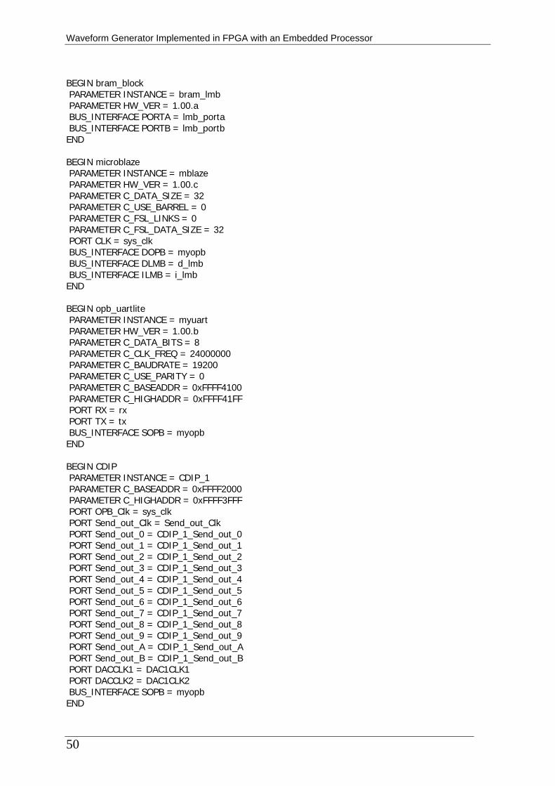
Waveform Generator Implemented in FPGA with an Embedded Processor
50
BEGIN bram_block PARAMETER INSTANCE = bram_lmb PARAMETER HW_VER = 1.00.a BUS_INTERFACE PORTA = lmb_porta BUS_INTERFACE PORTB = lmb_portb END BEGIN microblaze PARAMETER INSTANCE = mblaze PARAMETER HW_VER = 1.00.c PARAMETER C_DATA_SIZE = 32 PARAMETER C_USE_BARREL = 0 PARAMETER C_FSL_LINKS = 0 PARAMETER C_FSL_DATA_SIZE = 32 PORT CLK = sys_clk BUS_INTERFACE DOPB = myopb BUS_INTERFACE DLMB = d_lmb BUS_INTERFACE ILMB = i_lmb END BEGIN opb_uartlite PARAMETER INSTANCE = myuart PARAMETER HW_VER = 1.00.b PARAMETER C_DATA_BITS = 8 PARAMETER C_CLK_FREQ = 24000000 PARAMETER C_BAUDRATE = 19200 PARAMETER C_USE_PARITY = 0 PARAMETER C_BASEADDR = 0xFFFF4100 PARAMETER C_HIGHADDR = 0xFFFF41FF PORT RX = rx PORT TX = tx BUS_INTERFACE SOPB = myopb END BEGIN CDIP PARAMETER INSTANCE = CDIP_1 PARAMETER C_BASEADDR = 0xFFFF2000 PARAMETER C_HIGHADDR = 0xFFFF3FFF PORT OPB_Clk = sys_clk PORT Send_out_Clk = Send_out_Clk PORT Send_out_0 = CDIP_1_Send_out_0 PORT Send_out_1 = CDIP_1_Send_out_1 PORT Send_out_2 = CDIP_1_Send_out_2 PORT Send_out_3 = CDIP_1_Send_out_3 PORT Send_out_4 = CDIP_1_Send_out_4 PORT Send_out_5 = CDIP_1_Send_out_5 PORT Send_out_6 = CDIP_1_Send_out_6 PORT Send_out_7 = CDIP_1_Send_out_7 PORT Send_out_8 = CDIP_1_Send_out_8 PORT Send_out_9 = CDIP_1_Send_out_9 PORT Send_out_A = CDIP_1_Send_out_A PORT Send_out_B = CDIP_1_Send_out_B PORT DACCLK1 = DAC1CLK1 PORT DACCLK2 = DAC1CLK2 BUS_INTERFACE SOPB = myopb END

Appendix
51
BEGIN CDIP PARAMETER INSTANCE = CDIP_2 PARAMETER C_BASEADDR = 0xFFFF6000 PARAMETER C_HIGHADDR = 0xFFFF7FFF PORT OPB_Clk = sys_clk PORT Send_out_Clk = Send_out_Clk PORT Send_out_0 = CDIP_2_Send_out_0 PORT Send_out_1 = CDIP_2_Send_out_1 PORT Send_out_2 = CDIP_2_Send_out_2 PORT Send_out_3 = CDIP_2_Send_out_3 PORT Send_out_4 = CDIP_2_Send_out_4 PORT Send_out_5 = CDIP_2_Send_out_5 PORT Send_out_6 = CDIP_2_Send_out_6 PORT Send_out_7 = CDIP_2_Send_out_7 PORT Send_out_8 = CDIP_2_Send_out_8 PORT Send_out_9 = CDIP_2_Send_out_9 PORT Send_out_A = CDIP_2_Send_out_A PORT Send_out_B = CDIP_2_Send_out_B PORT DACCLK1 = DAC2CLK1 PORT DACCLK2 = DAC2CLK2 BUS_INTERFACE SOPB = myopb END BEGIN mybramctrl PARAMETER INSTANCE = mybramctrl_0 PARAMETER C_BASEADDR = 0xFFFF8000 PARAMETER C_HIGHADDR = 0xFFFF9FFF PORT OPB_Clk = sys_clk BUS_INTERFACE SOPB = myopb END BEGIN lmb_v10 PARAMETER INSTANCE = d_lmb PARAMETER HW_VER = 1.00.a PARAMETER C_EXT_RESET_HIGH = 0 PORT LMB_Clk = sys_clk PORT SYS_Rst = system_reset END BEGIN lmb_v10 PARAMETER INSTANCE = i_lmb PARAMETER HW_VER = 1.00.a PARAMETER C_EXT_RESET_HIGH = 0 PORT LMB_Clk = sys_clk PORT SYS_Rst = system_reset END BEGIN opb_v20 PARAMETER INSTANCE = myopb PARAMETER HW_VER = 1.10.a PARAMETER C_EXT_RESET_HIGH = 0 PORT SYS_Rst = system_reset PORT OPB_Clk = sys_clk END

Waveform Generator Implemented in FPGA with an Embedded Processor
52
############################################################## ## Microprocessor Software Specification file system.mss ############################################################## PARAMETER VERSION = 2.0.0 PARAMETER HW_SPEC_FILE = system.mhs BEGIN PROCESSOR PARAMETER HW_INSTANCE = mblaze PARAMETER DRIVER_NAME = cpu PARAMETER DRIVER_VER = 1.00.a PARAMETER EXECUTABLE = mblaze/code/executable.elf PARAMETER COMPILER = mb-gcc PARAMETER ARCHIVER = mb-ar PARAMETER OS = standalone PARAMETER DEFAULT_INIT = EXECUTABLE PARAMETER STDIN = myuart PARAMETER STDOUT = myuart PARAMETER SHIFTER = FALSE END BEGIN DRIVER PARAMETER HW_INSTANCE = myuart PARAMETER DRIVER_NAME = uartlite PARAMETER DRIVER_VER = 1.00.b PARAMETER LEVEL = 0 END ############################################################## ## Microprocessor Verification Specification file system.mvs ############################################################## PARAMETER HW_SPEC_FILE = system.mhs PARAMETER LANGUAGE = VHDL PARAMETER SIMULATOR = mti PARAMETER MTI_NODEBUG_LIB = C:/Xilinx/EDK/edk_nd_libs PARAMETER MTI_UNISIM_LIB = C:/Xilinx/unisim PARAMETER MTI_SIMPRIM_LIB = C:/Xilinx/simprim PARAMETER SIM_MODEL = STRUCTURAL

Appendix
53
############################################################## ## Microprocessor Peripheral Definition file CDIP_v2_0_0.mpd ############################################################## BEGIN CDIP, IPTYPE = PERIPHERAL, EDIF=TRUE BUS_INTERFACE BUS = SOPB, BUS_STD = OPB, BUS_TYPE = SLAVE ## Generics for VHDL or Parameters for Verilog PARAMETER C_BASEADDR = 0xFFFF4000, DT = std_logic_vector, MIN_SIZE = 0x1FFF PARAMETER C_HIGHADDR = 0xFFFF5FFF, DT = std_logic_vector PARAMETER C_OPB_AWIDTH = 32, DT = integer PARAMETER C_OPB_DWIDTH = 32, DT = integer PARAMETER C_MEMSIZE = 8192, DT = integer PARAMETER C_PORT_AWIDTH = 32, DT = integer PARAMETER C_PORT_DWIDTH = 32, DT = integer PARAMETER C_NUM_WE = 4, DT = integer # Global ports PORT OPB_Clk = "", DIR = IN, SIGIS=CLK, BUS=SOPB PORT Send_out_Clk = "", DIR = IN, SIGIS=SEND_OUT_CLK, BUS=SOPB PORT OPB_Rst = OPB_Rst, DIR = IN, BUS=SOPB # OPB slave signals PORT OPB_ABus = OPB_ABus, DIR=IN, VEC=[0:C_OPB_AWIDTH-1], BUS=SOPB PORT OPB_BE = OPB_BE, DIR=IN, VEC=[0:C_OPB_DWIDTH/8-1], BUS=SOPB PORT OPB_RNW = OPB_RNW, DIR=IN, BUS=SOPB PORT OPB_select = OPB_select, DIR=IN, BUS=SOPB PORT OPB_seqAddr = OPB_seqAddr, DIR=IN, BUS=SOPB PORT OPB_DBus = OPB_DBus, DIR=IN, VEC=[0:C_OPB_DWIDTH-1], BUS=SOPB PORT CDIP_DBus = Sl_DBus, DIR=OUT, VEC=[0:C_OPB_DWIDTH-1], BUS=SOPB PORT CDIP_errAck = Sl_errAck, DIR=OUT, BUS=SOPB PORT CDIP_retry = Sl_retry, DIR=OUT, BUS=SOPB PORT CDIP_toutSup = Sl_toutSup, DIR=OUT, BUS=SOPB PORT CDIP_xferAck = Sl_xferAck, DIR=OUT, BUS=SOPB PORT Send_out_0 = "", DIR=OUT PORT Send_out_1 = "", DIR=OUT PORT Send_out_2 = "", DIR=OUT PORT Send_out_3 = "", DIR=OUT PORT Send_out_4 = "", DIR=OUT PORT Send_out_5 = "", DIR=OUT PORT Send_out_6 = "", DIR=OUT PORT Send_out_7 = "", DIR=OUT PORT Send_out_8 = "", DIR=OUT PORT Send_out_9 = "", DIR=OUT PORT Send_out_A = "", DIR=OUT PORT Send_out_B = "", DIR=OUT PORT DACCLK1 = "", DIR=OUT PORT DACCLK2 = "", DIR=OUT END ############################################################## ## Peripheral Analyze Order file CDIP_v2_0_0.pao ############################################################## lib common_v1_00_a pselect lib CDIP core lib CDIP CDIP

Waveform Generator Implemented in FPGA with an Embedded Processor
54
#-------------------------------------------------------------------------------------------------------------------------- # Configuration file system.ucf #-------------------------------------------------------------------------------------------------------------------------- #-------------------------------------------------------------------- # Clock Period Constraints And Reset Constraints #-------------------------------------------------------------------- NET "sys_clk" PERIOD = 41.70; # 24 MHz NET "sys_clk" LOC = "A11"; NET "Send_out_Clk" PERIOD = 10.00; # 100 MHz NET "Send_out_Clk" LOC = "B11"; NET "system_reset" LOC = "B6"; NET "system_reset" PULLUP; #-------------------------------------------------------------------- # UART Lite #-------------------------------------------------------------------- NET "tx" LOC = "A7"; NET "rx" LOC = "B7"; #-------------------------------------------------------------------- # DAC 1 #-------------------------------------------------------------------- NET "CDIP_1_Send_out_0" LOC = "AA8"; #LSB NET "CDIP_1_Send_out_1" LOC = "U10"; NET "CDIP_1_Send_out_2" LOC = "AB7"; NET "CDIP_1_Send_out_3" LOC = "U9"; NET "CDIP_1_Send_out_4" LOC = "AA7"; NET "CDIP_1_Send_out_5" LOC = "V9"; NET "CDIP_1_Send_out_6" LOC = "AB6"; NET "CDIP_1_Send_out_7" LOC = "V8"; NET "CDIP_1_Send_out_8" LOC = "AA6"; NET "CDIP_1_Send_out_9" LOC = "V7"; NET "CDIP_1_Send_out_A" LOC = "AB5"; NET "CDIP_1_Send_out_B" LOC = "V6"; #MSB NET "DAC1CLK1" LOC = "AA5"; NET "DAC1CLK2" LOC = "U13"; #-------------------------------------------------------------------- # DAC 2 #-------------------------------------------------------------------- NET "CDIP_2_Send_out_0" LOC = "AB15"; #LSB NET "CDIP_2_Send_out_1" LOC = "Y17"; NET "CDIP_2_Send_out_2" LOC = "AA14"; NET "CDIP_2_Send_out_3" LOC = "W16"; NET "CDIP_2_Send_out_4" LOC = "AB14"; NET "CDIP_2_Send_out_5" LOC = "Y16"; NET "CDIP_2_Send_out_6" LOC = "AA13"; NET "CDIP_2_Send_out_7" LOC = "V16"; NET "CDIP_2_Send_out_8" LOC = "AB13"; NET "CDIP_2_Send_out_9" LOC = "W15"; NET "CDIP_2_Send_out_A" LOC = "AA12"; NET "CDIP_2_Send_out_B" LOC = "V14"; #MSB NET "DAC2CLK1" LOC = "AA17"; NET "DAC2CLK2" LOC = "U14";

Upphovsrätt
Detta dokument hålls tillgängligt på Internet – eller dess framtida ersättare –under en längre tid från publiceringsdatum under förutsättning att inga extra-ordinära omständigheter uppstår.
Tillgång till dokumentet innebär tillstånd för var och en att läsa, ladda ner,skriva ut enstaka kopior för enskilt bruk och att använda det oförändrat förickekommersiell forskning och för undervisning. Överföring av upphovsrättenvid en senare tidpunkt kan inte upphäva detta tillstånd. All annan användning avdokumentet kräver upphovsmannens medgivande. För att garantera äktheten,säkerheten och tillgängligheten finns det lösningar av teknisk och administrativart.
Upphovsmannens ideella rätt innefattar rätt att bli nämnd som upphovsman iden omfattning som god sed kräver vid användning av dokumentet på ovanbeskrivna sätt samt skydd mot att dokumentet ändras eller presenteras i sådanform eller i sådant sammanhang som är kränkande för upphovsmannens litteräraeller konstnärliga anseende eller egenart.
För ytterligare information om Linköping University Electronic Press seförlagets hemsida http://www.ep.liu.se/
Copyright
The publishers will keep this document online on the Internet - or its possiblereplacement - for a considerable time from the date of publication barringexceptional circumstances.
The online availability of the document implies a permanent permission foranyone to read, to download, to print out single copies for your own use and touse it unchanged for any non-commercial research and educational purpose.Subsequent transfers of copyright cannot revoke this permission. All other usesof the document are conditional on the consent of the copyright owner. Thepublisher has taken technical and administrative measures to assure authenticity,security and accessibility.
According to intellectual property law the author has the right to bementioned when his/her work is accessed as described above and to be protectedagainst infringement.
For additional information about the Linköping University Electronic Pressand its procedures for publication and for assurance of document integrity,please refer to its WWW home page: http://www.ep.liu.se/
© [2003, Anna Goman]