wavelength tuning devices based on liquid crystals...1.6 molecular structure of three nematic liquid...
TRANSCRIPT

WAVELENGTH TUNABLE DEVICES BASED ON HOLOGRAPHIC
POLYMER DISPERSED LIQUID CRYSTALS
A dissertation Submitted to
Kent State University
in partial fulfillment of the requirements
for the degree of
DOCTOR OF PHILOSOPHY
By Hailiang Zhang
May, 2008

Dissertation written by
Hailiang Zhang
B.S., Xiangtan University, 1987
M.S., Kent State University, 1999
Ph.D., Kent State University, 2008
Approved by
, Jack R. Kelly, Professor, Chair, Doctoral Dissertation Committee , Gregory P. Crawford, Professor, Members, Doctoral Dissertation Committee , Deng-Ke Yang, Professor, Members, Doctoral Dissertation Committee , Eugene C. Gartland, Jr, Professor, Members, Doctoral Dissertation Committee , Qi-Huo Wei, Assistant Professor, Members, Doctoral Dissertation Committee , Donald L. White, Professor, Members, Doctoral Dissertation Committee
Accepted by Oleg D. Lavrentovich , Chair, Liquid Crystal Institute Timothy S. Moerland , Dean, College of Arts and Sciences
ii

ZHANG, HAILIANG, Ph.D, May 2008 CHEMICAL PHYSICS
WAVELENGTH TUNABLE DEVICES BASED ON HOLOGRAPHIC POLYMER
DISPERSED LIQUID CRYSTALS, (222)
Director of Dissertation: Jack Kelly
Wavelength tunable devices have generated great interest in basic science, applied physics,
and technology and have found applications in Lidar detection, spectral imaging and optical
telecommunication. This thesis focuses on the physics, technology and application of several
wavelength tunable devices based on liquid crystal technology, especially on Holographic
Polymer Dispersed Liquid Crystals (HPDLC).
HPDLCs are formed through the photo-induced polymerization process of
photopolymerizable monomers, and self-diffusion process and phase separation process of the
mixture of liquid crystals and monomers, when the mixtures of liquid crystals and monomers are
exposed to the interfering monochromatic light beams. The infomation from the interfering
pattern is recorded into the holographic liquid crystal/polymer composites, which are switchable
or tunable upon external electric fields.
Based on the electrically controllable beam steering capability of transmission HPDLCs,
novel switchable circular to point converter (SCPC) devices are demonstrated for selecting and
routing the wavelength channels discriminated by a Fabry-Perot interferometer, with application
in Lidar detection, spectral imaging and optical telecommunication. SCPC devices working in
both visible and near infrared (NIR) wavelength ranges are demonstrated. A random optical
switch can be created by integrating a Fabry-Perot interferometer with a stack of SCPC units.
iii

Liquid crystal Fabry-Perot (LCFP) Products have been analyzed, fabricated and characterized
for application in both spectral imaging and optical telecommunication. Both single-etalon system
and twin-etalon system are fabricated. Finesse of more than 10 in visible wavelength range and
finesse in more than 30 in NIR are achieved for the tunable LCFP product.
The materials, fabrication and characterization of lasing emission of dye doped HPDLCs are
discussed. Lasing from different modes of HPDLCs is studied and both the switching and
tunability of the lasing function is demonstrated. Lasing from two-dimensional HPDLC based
Photonic Band Gap (PBG) materials will also be demonstrated. Finally, lasing from polarization
modulated grating is discussed.
iv

TABLE OF CONTENTS
LIST OF FIGURES ........................................................................................................................ ix
LIST OF TABLES......................................................................................................................xviii
ACKNOWLEDGEMENT ............................................................................................................ xix
CHAPTER I. INTRODUCTION TO LIQUID CRYSTALS ......................................................... 1
Physical Properties of Liquid crystals.............................................................................................. 1
Liquid crystal phases........................................................................................................................ 1
Anisotropic properties of liquid crystals.......................................................................................... 5
The Frank Free Energy and the continuum theory .......................................................................... 9
Surface Alignment of Liquid crystal.............................................................................................. 11
Modeling of Director Configuration of Liquid Crystals ................................................................ 13
Director configuration in case of infinite surface anchoring ......................................................... 13
Director configuration in case of finite surface anchoring............................................................. 21
CHAPTER 2. LIGHT PROPAGATION IN STRATIFIED MATERIALS .................................. 24
Introduction.................................................................................................................................... 24
Jones matrix method ...................................................................................................................... 26
Berreman's 4-by-4 matrix method ................................................................................................. 29
Light Propagation in Periodic Media ............................................................................................. 37
Introduction to grating ................................................................................................................... 37
Coupled Wave Theory .................................................................................................................. 40
v

Coupled wave theory for transmission Gratings............................................................................ 42
Coupled wave theory for reflection Gratings................................................................................. 48
CHAPTER 3. HOLOGRAPHIC POLYMER DISPERSED LIQUID CRYSTAL........................ 52
Introduction to Holography............................................................................................................ 52
Introduction to holographic polymer dispersed liquid crystals...................................................... 54
Transmission Mode HPDLCs ........................................................................................................ 57
Reflection Mode HPDLC .............................................................................................................. 60
Variable-Wavelength HPDLC ....................................................................................................... 62
HPDLC Materials .......................................................................................................................... 65
UV Mixtures .................................................................................................................................. 65
Visible Mixtures ............................................................................................................................ 66
Summary........................................................................................................................................ 67
CHAPTER 4. LIQUID CRYSTAL FABRY-PEROT ................................................................... 68
Introduction.................................................................................................................................... 68
Introduction to Fabry-Perot interferometer.................................................................................... 68
Introduction to Liquid Crystal Fabry-Perot (LCFP) Tunable Filter............................................... 79
Fabrication and Testing of LCFP Tunable Filter ........................................................................... 84
Single LCFP system....................................................................................................................... 84
Twin LCFP system ........................................................................................................................ 91
Environment Test of LCFP............................................................................................................ 93
Summary and Conclusions ............................................................................................................ 98
CHAPTER 5 SWITCHABLE CIRCLE-TO-POINT CONVERTER............................................ 99
Introduction.................................................................................................................................... 99
Background: Introduction to HCPC............................................................................................... 99
vi

Principle of Operation of SCPC................................................................................................... 102
Optics Design of SCPC................................................................................................................ 104
First type (beam steering) SCPC.................................................................................................. 104
Second type (focusing) SCPC...................................................................................................... 107
Astigmatism in second type (focusing) SCPC............................................................................. 108
Fabrication and characterization of SCPC working in visible wavelengths ................................ 113
Single channel SCPC ................................................................................................................... 113
Fabrication and Characterization of SCPC working in NIR wavelengths ................................... 118
Material optimization for big-area SCPC working in NIR .......................................................... 118
Fabrication and Characterization of single channel SCPC working in NIR................................ 121
Fabrication and Characterization of 32-channel SCPC working in NIR ..................................... 123
Summary and Conclusions .......................................................................................................... 133
CHAPTER 6. LASING OF DYE-DOPED HPDLC.................................................................... 134
Introduction.................................................................................................................................. 134
Introduction to Dye...................................................................................................................... 134
Introduction to laser ..................................................................................................................... 139
Introduction to dye laser .............................................................................................................. 144
Introduction to Photonic Band Gap Materials ............................................................................. 149
Introduction to Lasing in Liquid Crystal Materials ..................................................................... 150
Introduction to Dye-Lasing in HPDLC........................................................................................ 152
Dye Lasing from HPDLC of Different Modes: Materials, Fabrications and Results .................. 154
Lasing of single reflective dye-doped HPDLC............................................................................ 154
Lasing of transmissive dye-doped HPDLC ................................................................................. 157
Multiple-Method for Lasing Tuning............................................................................................ 167
vii
Lasing Tuning in Stack of HPDLCs ............................................................................................ 166
Lasing Tuning in chirped HPDLC............................................................................................... 169
Two Dimensional Dye-Doped HPDLC Lasing ........................................................................... 172
Lasing of Polarization Grating..................................................................................................... 178
Summary and Conclusions .......................................................................................................... 188
CHAPTER 7 CONCLUSIONS AND CONSIDERATION ON FUTURE WORK................... 189
BIBLIOGRAPHY........................................................................................................................ 191
viii
LIST OF FIGURES
Figure Page
1.1 Schematic description of crystal, liquid crystal and liquid 2
1.2 Schematic description of smectic phase 3
1.3 Schematic description of director Orientation of Cholesteric state 3
1.4 Definition of θ used in equation (1-1) 4
1.5 Order parameter S changes with the temperature T 5
1.6 Molecular structure of three nematic liquid crystals 7
1.7 Director re-orientation in the external field 8
1.8 Three canonical elastic distortions: (a) bend (b) Twist and (c) Splay 10
1.9 Planar or homogeneous alignment of nematic liquid crystals 11
1.10 The direction of a nematic liquid crystal on a solid surface, 0n
specified by the polar angle 0θ and azimuthal angle 0φ . 13
1.11 Co-odinator system of director 14
1.12 Director configuration of 90° twist cell without applied voltage (a), and
under applied voltage of 5V (b) 19
1.13 Director configuration of a chiral-doped homeotropicly aligned cell 20
1.14 Director configuration of a chiral-doped homeotropic-alignment cell with
finite surface anchoring, with no applied voltage 22
1.15 Z-component of the director of a chiral-doped homeotropic-alignment cell
at different surface anchoring strength 23
ix

2.1 Local coordinator system - - z in Jones matrix method 27 xE yE
2.2 Spectral response of clock-wise circularly-polarized light
from two cholesteric cells 37
2.3 Diffraction of a monochromatic plane wave by an optically thick grating 38
2.4 Diffraction of a monochromatic plane wave by an optically thin grating 40
2.5 Diffraction by optically thick gratings. (a) Transmission grating;
(b) Reflection grating 41
2.6 K-space of transmission gratings (a) Ideal phase match 0=αΔ ; (b)
not ideal phase match 0≠Δα . 43
2.7 Phase mismatch in transmission gratings due to (a) angular deviation;
and (b) wavelength deviation 45
2.8 The diffraction efficiency decreases with the increase of phase mismatch. 46
2.9 Diffraction efficiency as a function of phase mismatch (Δβ/2k) for
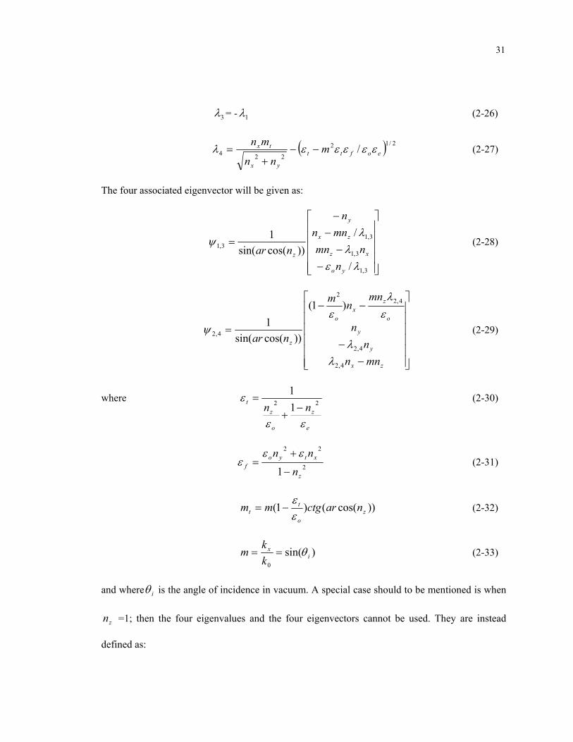
reflection gratings with different thickness kL. 48
2.10 Diffraction efficiency of a reflection grating as a function of Lκ
for an ideally matched phase Δβ/2k. 50
2.11 Modeling of reflection grating at normal incidence. Berreman’s 4x4 method
and coupled wave theory calculation are compared. 51
3.1 Optical setup for recording (a) and reconstructing (b) in-line hologram 53
3.2 The optical setup for recording (a) and reconstructing (b) off-line hologram 53
3.3 Holographic configurations for (a) reflective mode and
(b) transmissive mode HPDLCs 56
3.4 Transmission HPDLCs in the (a) on state; (b) off state 58
x

3.5 Polarization independent electro-optical device based on stacking of two
polarization sensitive transmission HPDLCs (G1 and G2) and a
polarization rotator (PR) 59
3.6 The SEM photograph of a transmission HPDLC operating at 1500 nm.
top substrate is pealed before SEM photograph is taken 60
3.7 The SEM photograph of a reflective HPDLC operating at ~1500 nm.
The image is of the cross section of a cell 61
3.8 Schematic illustration of a reflecting variable-wavelength HPDLC 63
3.9 (a) Reflectance and peak reflected wavelength as a function of applied
voltage for variable wavelength HPDLC with a 5 μm cell gap.
(b) Experimentally (points) and modeled (curves) reflectance
spectra of variable wavelength HPDLC measured at 0, 120, and 220 V 64
4.1 Diagram of a plate with refraction index n immersed in the
boundary media with refraction index of 'n 69
4.2 Behavior of as a function of the phase difference δ for various )()( / it II
values of finesse Ғ 72
4.3 Fabry-Perot interferometer 73
4.4 Image of the Fabry-Perot interference pattern with
monochromatic incident light 74
4.5 Relation of the reflective finesse with the reflectivity 75
4.6 Spherical defects (a), surface irregularities (b), and parallelism defects (c) 75
4.7 Effective finesse changes with the defect finesse. FR represents the
reflective finesse 76
4.8 Modeling of twin etalon system with the gaps of 3 micron and 12 micron 78
xi

4.9 Structure of liquid crystal Fabry-Perot 80
4.10 The average refraction index changes with the applied voltages 81
4.11 Combination of polarization beam splitter and two LCFPs with
alignment directions perpendicular to each other, to achieve the
polarization-independent wavelength filtering 82
4.12 Two LC layers inside the Fabry-Perot Cavity to achieve the polarization
independent wavelength filtering and tuning 83
4.13 Twist nematic Fabry-Perot 84
4.14 Spectral response of LCFP #1608, measured at 1.5 V 87
4.15 Spectral response of LCFP #1608, measured at 3.5 V 88
4.16 Spectral response of LCFP #1608, measured at 9.0 V 89
4.17 Electro-optical response of LCFP #1608, measured at 805 nm 90
4.18 LCFP #1608 in the housing with electrical connector 90
4.19 Photographs of the single etalon in the housing (right) and
the twin etalon imaging filter (left) 91
4.20 Transmission as a function of wavelength for the 30 μm gap LCFP 92
4.21 Transmission as a function of wavelength for the 6 μm gap LCFP 93
4.22 Temperature versus time for the thermal vacuum testing of the LCFP 95
4.23 Transmission of the LCFP that underwent a Pegasus-level shake test
for two different voltage settings (1 and 9 Volt) 96
4.24 Transmission of the LCFP that underwent thermal cycling,
before and after the thermal cycling for two different voltage settings 97
5.1 The ray trace diagram of the holographic circular-to-point converter
(HCPC) developed by McGill and co-workers 101
xii

5.2 The cross-section drawing of a 4X2 switch employing two identical SCPC
Elements 103
5.3 A random optical cross-switch can by stacking multiple SCPC units 103
5.4 The first type of SCPC: the diffracted beam is focused
by a focal lens to a point. 104
5.5 Reading beam configuration (a) and recording beam configuration
(b) of the beam steering HPDLLC for the first type of SCPC. 105
5.6 The holography setup for fabricating the second type SCPC 107
5.7 Recording beam profile across the HPDLC area using
the setup in Figure 5.6 108
5.8 The diffraction beam profile of 1 inch HPDLCs fabricated using
focal lenses with various focal length F 112
5.9 The left panel : the switch-off state of the SCPC (no voltage applied);
the right panel : the switch-on state (voltage applied). In each panel,
the holographic focal point is the point on the right side, and the
“pass-through” light is on the left 113
5.10 Switching of a SCPC working in 532 nm 115
5.11 A schematic description of CAD design of a 10-pixel ITO pattern in SCPC 116
5.12 Switching of the center pixel of 10-pixel type-II SCPC 117
5.13 Switching of one non-center pixel of 10-pixel type-I SCPC 117
5.14 Switch on the center pixel of a beam-steering 10-channel SCPC 118
5.15 Holographic recording setup for fabricating the SCPCs working
in 1550 nm range 121
5.16 Transmittance and diffraction efficiency as a function of voltage 122
xiii

5.17 Switching of independent channels in the SCPC unit. The photos, show that
the deactivation of the central pixel, the 5th pixel (count from the center),
and the outmost pixel(32th), respectively. 124
5.18 The normalized transmittance and diffraction efficiency of the center
channel of a SCPC unit as the function of voltage 125
5.19 Optical setup for measuring the wavelength dependence of the SCPC units 126
5.20 Transmittance and diffraction efficiency as a function of wavelength
of the switch-off state of a SCPC sample: JL101404B 127
5.21 The fitting of the modeling result based on coupled wave theory and the
refraction principle, with the measurement result, for the wavelength
dependence of the diffraction efficiency 129
5.22 The transmission as a function of incident angle of the SCPC 130
5.23 The diffraction efficiency as a function of incident angle of the SCPC 131
5.24 Normalized transmittance is fitted to the formula for transmission grating
derived using coupled wave theory 132
6.1 Absorption of positive dye (a) and negative dye (b) 135
6.2 Two basic kinds of dyes (a) azo dye (b) anthraquinone dye 136
6.3 Dye molecules inside liquid crystals 138
6.4 (a) Two-level energy system of laser medium.
(b) three-level energy system 140
6.5 A four-level laser energy diagram. 143
6.6 Molecular structure of the lasing dye Pyrromethene 580(a) and DCM(b) 145
6.7 Emission spectrum of a dye molecule shifts from the absorption spectrum 147
6.8 “Littrow arrangement” tunes of the center peak of a laser
xiv

by rotating the diffraction grating 148
6.9 Lasing emission from a reflection mode HPDLC (solid line) and
transmission spectra of the same sample (dotted line) 155
6.10 Switching of the dye lasing emission from a reflection mode HPDLC 156
6.11 Two lens were used to generate the vertical line across the HPDLC
grating in order to increase the area of the gain medium being pumped 157
6.12 Lasing emission of the sample with 0.5% Dye concentration as the pump
beam polarization is changed from s-polarized to p-polarization. 159
6.13 Lasing emission of the sample with 1% Dye concentration as the pump
beam polarization is changed from s-polarized to p-polarization. 160
6.14 Lasing emission of the sample with 2% Dye concentration as the pump
beam polarization is changed from s-polarization to p-polarization 161
6.15 Dye molecules are distributed in the liquid crystal layers and are aligned
with the liquid crystal in the surface. 162
6.16 Lasing emission at various pump energies in a sample with 0.5% dye. 163
6.17 Lasing emission at various pump energies in a sample with 1% dye. 164
6.18 Peak emission intensity at various pump energies. A threshold at ~18 µJ.
Sample has dye concentration of 0.5%. 164
6.19 Effect of electric fields on lasing in a transmission HPDLC. Energy of
pumping laser is 20 μJ. 165
6.20 Various modes of operation to tune the wavelength peak of the lasing. 167
6.21 Stacked grating for tunable lasing. The grating with the smaller
pitch, lower reflection band in a zero voltage state, while the larger pitch
grating has a field applied across it to switch off lasing. 167
xv

6.22 Transmission of the two gratings used in the stack. A is doped with dye
P580, and grating B is doped with dye DCM. 168
6.23 Tuning of a chirped HPDLC. Transmission at left (solid), middle (dashed)
and right (dotted) points (top); and lasing emission at left (solid),
middle (dashed) and right (dotted) points on the sample (bottom). 171
6.24 Switching of a reflection mode chirped HPDLC. 171
6.25 (a) Setup for creating 4-beam interference pattern and (b) the interference
pattern; the bright (dark) regions represent areas of high (low) intensity. 174
6.26 SEM image of a HPDLC lattice generated by 4-beam interference.
The designed period is 222nm. 174
6.27 (a) Setup for creating 6-beam interference pattern (b) the interference
pattern; the bright (dark) regions represent areas of high (low) intensity. 175
6.28 (a) Isointensity plot for four-beam fabrication ; and (b) lasing from this structure
doped with the laser dyes Pyrromethene 580 (solid line) and DCM (dotted line).
Lasing emission is measured along x-direction. 176
6.29 (a) Isointensity plot for six-beam fabrication and
subsequently lasing; and (b) lasing from this structure doped with the
laser dyes Pyrromethene 580 (solid line) and DCM (dotted line). 177
6.30 a) Two linearly polarized beams with orthogonal polarization directions;
(b)Two circularly polarized beams with opposite sense of clockwise 182
6.31 Microscope images of a cell of polarization grating between polarizers.
(a) no voltage is applied; (b) 20 V voltage is applied 183
6.32 Writing beam and pump beam for fabrication and lasing emission
testing of the polarization gratings 183
xvi

6.33 Lasing emission from a liquid crystal polarization holography grating. 184
6.34 Threshold of laser emission for the dye-doped polarization grating 184
6.35 lasing emission increases by 50% as the incident polarization is rotated 186
6.36 Effect of an applied electric field on a liquid crystal polarization
grating pumped by p-polarized light. 187
xvii

LIST OF TABLES
4.1 Finesse and free spectral range of LCFP # 1608 at different voltages 86
4.2. Testing result of tunable LCFP for tunable laser in NIR range 86
5.1. Converging recording beam incident angle, Bragg reading and
diffraction angles, diffraction angles with normal incident reading, and
minimum distance between neighboring SCPC units. 110
5.2 Testing result of SCPC 115
5.3 Components of the HPDLC mixtures initially investigate 120
5.4 Material contents of Formula-SCPC 121
5.5 The transmittance of some channels of a SCPC unit 125
xviii
ACKNOWLEDGEMENT
I would like to thank my two advisors, Professor Gregory P. Crawford and Professor Jack
Kelly, for all their education, instruction, and support.
During the three years I studied and worked in the Liquid crystal Institute of Kent State
University from 1996 to 1999, I had learned a lot from all the professors and teachers. I would
like to express my gratitude to all of them.
I would like to thank Scientific Solutions, Inc., the company I have worked for since late
2000, for providing a great research platform for me to continue my PhD research. I also thank
the Display and Photonics lab of Brown University for the happy cooperation on all the research
projects I have done during these years, especially, with special gratitute to Professor Gregory P.
Crawford who has given me so many support, direction and inspiration.
I got a lot of help from Dr. Haiqing Xianyu, Mr. Scott Woltman (PhD candidate), Mr. Jianhua
Lian, Dr. Jun qi, and Dr. Matthew Sousa from Display and Photonics lab of Brown University. I
would like to thank all of them for their assistance and helpful discussions.
Special gratitude to my family, especially my parents, for their long-term support and
encouragement. I would like to use my dissertation as a special gift to my lovely daughter,
hopefully she will like it more than a toy.
Finally, I would like to thank my Small Business Innovation Research (SBIR) project
sponsors: National Science Foundation, NASA and Department of Energy.
xix
CHAPTER I
Introduction to Liquid Crystals
1.1 Physical Properties of Liquid Crystals
The liquid crystal phase is an intermediate state between the solid crystalline phase and the
isotropic liquid phase (Fig. 1.1). The distinguishing characteristic of the liquid crystalline state is
the tendency of the molecules (mesogens) to point along a common axis, called the director. This
is in contrast to molecules in the liquid phase, which have no intrinsic order. In the solid state,
molecules are highly ordered and have little translational freedom. The characteristic orientational
order of the liquid crystal state is between the traditional solid and liquid phases; this is the origin
of the term mesogenic phase, used synonymously with the liquid crystal state. Liquid crystals
exhibit some degree of fluidity, which may be comparable to that of an ordinary liquid; However
they also exhibit anisotropies in their optical, electrical, magnetic and other physical properties
like crystals.
1.1.1 Liquid Crystal Phases
Liquid crystal phases are observed in certain organic compounds and usually are made up of
elongated molecules. There are a number of distinct liquid crystal between the crystalline phase
and the isotropic liquid. These intermediate transitions may be brought about by temperature
variation; the compounds in which the liquid crystal phase is induced by a thermal process are
known as thermotropic liquid crystals. The thermotropic liquid crystals are further classified into
three types: nematic, smectic and cholesteric as proposed by Friedel [1]. This classification is
1

2
based on the molecular arrangement and the ordering of the molecules in the particular liquid
crystal phases.
Nematic liquid crystals have long-range orientational order but no long-range translational
order. The average orientation of all of the molecules in the nematic liquid crystals is defined as
the director, as shown as the arrow in Fig. 1.1(b). Smectic liquid crystals (Fig. 1.2) are different
from nematics in that they have an additional degree of positional order. Smectics generally form
layers within which there is a loss of positional order, while the orientational order is still
preserved. There are several different categories to describe smectics. The two best known of
these are Smectic A, in which the molecules tend to align perpendicular to the layer planes, and
Smectic C, where the alignment of the molecules is at some arbitrary angle to the normal.
(a) (b) (c)
Fig. 1.1 Schematic description of crystal (a), liquid crystal (b) and liquid (c).
The cholesteric phase (or chiral nematic phase) is typically composed of nematic mesogenic
molecules containing chiral center that produces intermolecular forces, which favor an alignment
between molecules at a slight angle to one another. This leads to the formation of a structure that
can be visualized as a stack of very thin 2-D nematic-like layers with the director in each layer
twisted with respect to those above and below (Fig. 1.3). In this structure, the directors actually

3
form a continuous helical pattern about the layer normal. The black arrows in the Fig. 1.3
represent the director orientation in the succession of layers along the stack. An important
characteristic, the pitch, p, is defined as the distance it takes for the director to rotate one full turn.
(a) (b)
Fig.1.2. Schematic description of smectic phase. smectic A phase (a); smectic C phase (b).
Fig 1.3. Schematic description of director orientation of cholesteric state. Arrows
represent the director directions in each layer.
4
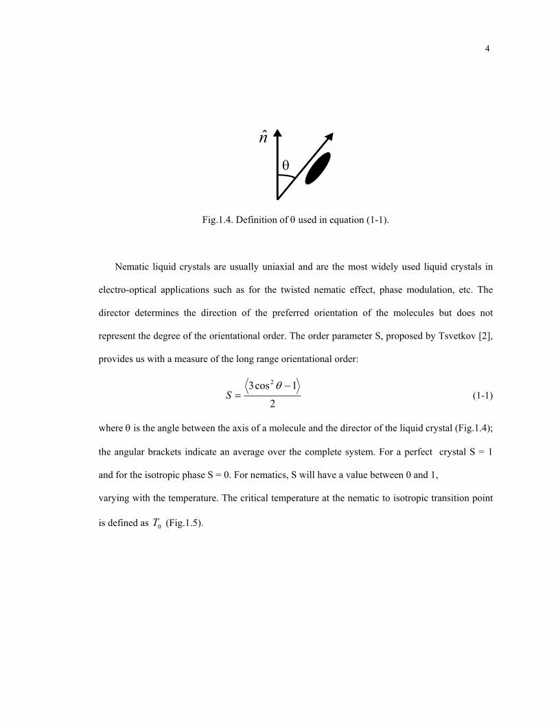
n̂θ
Fig.1.4. Definition of θ used in equation (1-1).
Nematic liquid crystals are usually uniaxial and are the most widely used liquid crystals in
electro-optical applications such as for the twisted nematic effect, phase modulation, etc. The
director determines the direction of the preferred orientation of the molecules but does not
represent the degree of the orientational order. The order parameter S, proposed by Tsvetkov [2],
provides us with a measure of the long range orientational order:
2
1cos3 2 −=
θS
(1-1)
where θ is the angle between the axis of a molecule and the director of the liquid crystal (Fig.1.4);
the angular brackets indicate an average over the complete system. For a perfect crystal S = 1
and for the isotropic phase S = 0. For nematics, S will have a value between 0 and 1,
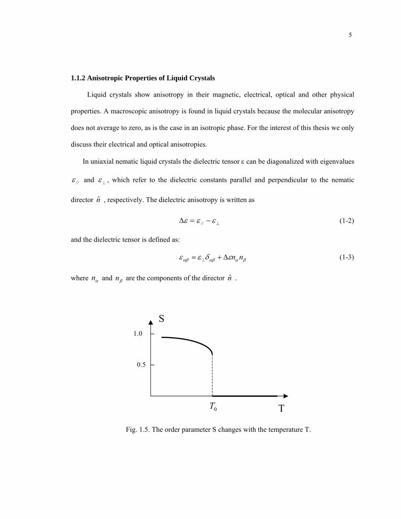
varying with the temperature. The critical temperature at the nematic to isotropic transition point
is defined as (Fig.1.5). 0T
5
1.1.2 Anisotropic Properties of Liquid Crystals
Liquid crystals show anisotropy in their magnetic, electrical, optical and other physical
properties. A macroscopic anisotropy is found in liquid crystals because the molecular anisotropy
does not average to zero, as is the case in an isotropic phase. For the interest of this thesis we only
discuss their electrical and optical anisotropies.
In uniaxial nematic liquid crystals the dielectric tensor ε can be diagonalized with eigenvalues
//ε and ⊥ε , which refer to the dielectric constants parallel and perpendicular to the nematic
director , respectively. The dielectric anisotropy is written as n̂
⊥−=Δ εεε // (1-2)
and the dielectric tensor is defined as:
βααβαβ εδεε nnΔ+= ⊥ (1-3)
where and are the components of the director . αn βn n̂
0.5
1.0
S
T0T
Fig. 1.5. The order parameter S changes with the temperature T.
6
The theoretical consideration [3] suggests that
0
////
321
εαρ
εε
=+−
(1-4)
032
1εαρ
εε ⊥⊥ =
+−
(1-5)
where 32// ⊥+
=εε
ε is the average dielectric co-efficient that does not depend on the order
parameter. //α and ⊥α are the average molecular polarizability when the applied field is
parallel or perpendicular to the director, respectively. For molecules without permanent dipoles,
Sααα Δ+=32
// (1-6)
Sααα Δ−=⊥ 31
(1-7)
where S is the order parameter and
3/)2( // ⊥+= ααα (1-8)
⊥−=Δ ααα // (1-9)
//α and ⊥α are the molecular polarizability along the long molecular axis direction or
perpendicular to the long molecular axis, respectively.
For molecules with permanent dipoles, (1-6) and (1-7) should be modified to include the
dipole term:
S
KTKT
pppp )2
1
(32
3
22//22
////
⊥⊥
−+Δ+
++=
μμα
μμαα (1-10)

7
S
KTKT
pppp )2
1
(31
3
22//22
//⊥
⊥⊥
−+Δ−
++=
μμα
μμαα (1-11)
where //pμ or ⊥pμ are the components of permanent dipole μr along the long-molecular axis or
perpendicular to the long-molecular axis, respectively.
NN
C7H15C7H15
(a)
C7H15 CN
(b)
C
N
C2H5O
OC6H15
(c)
Fig.1.6. Molecular structure of three nematic liquid crystals: (a) a non-polar liquid crystal
molecule; (b) a polar liquid crystal molecule with positive dielectric anisotropy; (c) a polar liquid
crystal molecule with negative dielectric anisotropy.

8
From (1-10) and (1-11) we can see that when there is a large angle between the permanent
dipole and the long molecular axis direction, //pμ < ⊥pμ and KT
pp22
// 21
⊥−+Δ
μμα may be
negative; therefore, //α < ⊥α and from (1-4) and (1-5) we find //ε < ⊥ε or 0<Δε .
Fig. 1.6 shows three kinds of nematics liquid crystals. (a) is a non-polar molecule while (b) is
a polar molecule with a dipolar moment parallel to the long molecular axis, thus
0)()( >Δ>Δ ab εε . In molecule (c) the CN group introduces a large permanent dipole moment
at a large angle with the long molecular axis direction, so 0)( <Δ cε .
The dielectric anisotropy introduces body torque on the molecules in the presence of an
external field, which in turn gives rise to the director re-orientation. (Fig.1.7) This property can be
used for liquid crystal materials with both positive and negative dielectric anisotropies. Under an
external field, the director of a liquid crystal with a positive dielectric anisotropy tends to align
parallel to the external field, while the director of a liquid crystal with a negative dielectric
anisotropy tends to align perpendicular to the external field.
Electric Field
Fig.1.7 Director re-orientation in the external field

9
Liquid crystals are also found to have optical anisotropy, or birefringence, due to their
anisotropic nature. They demonstrate double refraction, or light polarized parallel to the director
has a different index of refraction (that is to say it travels at a different velocity) than light
polarized perpendicular to the director. The optical anisotropy, or birefringence is given by:
oe nnn −=Δ
(1-12)
Where is the ordinary index of refraction, and is the extraordinary index of refraction. The
relation between the optical anisotropy and the dielectric anisotropy is given by:
on en
and (1-13) ;2
on=⊥ε 2// en=ε
1.2 The Frank Free Energy and the Continuum Theory
In a liquid crystal system, the bulk free energy of an inhomogeneous sample has contributions
from the elastic deformation of the system. The elastic properties of liquid crystals influence the
behaviors of these materials in an electric or magnetic field. The simplest way to treat the
deformation of a nematic liquid crystal is to consider it to be a continuous elastic medium,
disregarding the details of the molecular structure. The state of the system is described by the
director field , which determines the elastic free energy of the system. The stiffness of the
system can be expressed by a fourth rank tensor [4]:
n(r)
,21= 3
lkjiijklel nnxKdF ∇∇∫ where is a
tensor that generally depends on the local director . Considering the symmetry of the
nematic liquid crystal, the free energy should be invariant under the symmetry operation
. is a unit vector; therefore,
ijklK
n(r)
nn −→ n iji nn ∇ is zero. These factors indicate that when the bulk
energy is considered, has three independent components, which can be designated as elastic ijklK

10
constants , , , as depicted in Fig. 1.8. The first distortion, splay, is described by 11k 22k 33k n⋅∇ .
The second kind of distortion, twist, is described by )( nn ×∇⋅ . The third distortion, bend, is
evaluated by . )( nn ×∇×
In the continuum theory, first stated by Oseen [5] and Zocher [6], and completed by Frank
[7], the Frank free energy density of a nematic liquid crystal medium with a curvature
deformation in its director field is
}))ˆ(ˆ())ˆ(ˆ()ˆ({21 2
332
222
11 nnknnknkf ×∇×+×∇•+•∇=
(1-14)
Where , and correspond to the elastic constants of splay, twist and bend, respectively.
The surface elastic constants have been ignored in (1-14); they tend to play a larger role in highly
confined liquid crystal systems [130]. This form of the Frank free energy density is minimized
when the director is spatially uniform.
11k 22k 33k
(a) (b) (c)
Fig.1.8. Three canonical elastic distortions: (a) bend (b) twist and (c) splay.

11
For cholesteric liquid crystals, there are spontaneous twists, which are originated by the chiral
molecules. An additional term that takes into account the chirality of the molecules is introduced
in the second term of (2-14) resulting in the expression:
}))ˆ(ˆ())ˆ(ˆ()ˆ({
21 2
332
0222
11 nnkqnnknkf ×∇×++×∇•+•∇=
(1-15)
where 00 /2 pq π= is the wave vector; is the pitch of cholesteric. Positive and negative
values of correspond to a left or right-handed helix, respectively.
0p
0q
1.3 Surface Alignment of Liquid Crystal
In many liquid crystal devices, such as twisted nematic cells and waveplates, a uniform or
well-defined orientation of the liquid crystal molecules is required. Without surface alignment
and cell confinement, the liquid crystal cell will have multiple domains with different
orientations, and boundary walls and defects between the domains. The multi-domain nature and
the existence of numerous boundary walls and defects result in strong scattering. Specially treated
surfaces are employed in order to ensure a single domain in the designated area.
(a) ( b)
Fig. 1.9. Planar or homogeneous alignment (a) and homeotropic alignment (b) of nematic liquid
crystals.

12
Two types of surface alignment, as shown in Fig. 1.9, are widely used in liquid crystal
devices, distinguished by the preferred orientation of the molecules on the surface. With planar
or homogeneous alignment, the molecules are oriented in a direction parallel to the surface;
whereas with homeotropic alignment, the molecules are oriented in a direction perpendicular to
the surface. Planar alignment can be achieved by unidirectionally rubbing a coated polyimide
layer [8], or by exposing photo-alignable polyimide to polarized UV light [9]. Homeotropic
alignment is realized by depositing amphiphilic molecules such as lecithin [10], silane [11], or
some polyimides, such as SE-7511 from Brewer Science, on the surface.
A surface anchoring term is introduced into the free energy with the consideration of the
alignment effect. In the vicinity of the treated surface, there is an energetically favorable direction
given by a unit vector . In the model presented by Rapini and Papoular, the surface free energy
density is given by [12]:
0n
( ) constwwfsurf +−⋅− )(sin21=
21= 22 θ0s nn (1-16)
where is the anchoring strength, is the director at the surface; and θ is the angle
between and . The typical value of is in the order of J/
w sn
sn 0n w 74 10~10 −− 2m [13].
When an electric field is applied to a nematic liquid crystal cell, the spatial molecular
configuration can be determined by minimizing the free energy of the system:
surfefieldel FFFF ++=
})]([)]([)({21= 2
32
22
13 nnnnn ×∇×+×∇⋅+⋅∇∫ KKKxd
+ ( ) ∫∫ +⋅Δ− )](sin[21][ 223 θε wdSExd 0n
r (1-17)

13
θ
sn
0n
Fig. 1.10. The direction of a nematic on a solid surface, specified by the polar angle 0n 0θ and
azimuthal angle 0φ .
1.4. Modeling of Director Configuration of Liquid Crystals
The basic concept of director configuration modeling is to find the director configuration that
minimizes the total free energy of the system. The total free energy includes the bulk term, which
is described as the Frank-Oseen strain free energy, the surface term, which is surface free energy,
and the term related to the external electric field. For the surface term, both the two cases are
discussed: infinite surface anchoring and finite surface anchoring.
1.4.1 Director Configuration in Case of Infinite Surface Anchoring
When the surface anchoring energy is strong enough to be treated as infinite, the free energy
density equation for a liquid crystal material in an electric field, based on the Frank-Oseen strain
free energy density, is given by [7]:
EDnnkqnnknkf •±×∇×+−×∇•+•∇=21})]([])([)({
21 2
332
0222
11))))) (1-18)

14
where is the director and n̂ pq /20 π= , p is the natural pitch of the material; and , ,
are the splay, twist, and bend elastic constants, respectively. In the
11k 22k
33k ED •±21
term, D is the
electric flux density and E is the electric field; “ + ” is for the case of constant electric flux
density and “−” is for the case of constant electric field. In our application we usually consider the
applied voltage as a constant, so we concentrate on the latter constant voltage condition.
Assuming the director only changes along the cell normal, defined as the z-axis, a one-
dimensional condition, we use the coordinate system shown in Fig.1.11.
y
x
zn
xnyn
zn
Fig.1.11. Co-odinator system of director
It is reasonable to assume there is no free charge in the liquid crystal; from Maxwell’s
Equation we have 0=•∇ D 0=dz
dDz . Also, considering the constant voltage,
(1-19) VEdz =∫

15
So from Vdznn
D
zz
z =−+
∫⊥ )]1([ 22
//0 εεε (1-20)
We obtain
)1( 22//
0
0
zz
dz
nndzV
D
−+∫
=
⊥εε
ε (1-21)
This means the normal component of D is constant throughout the cell. The free energy can now
be written as:
]})()([][)({21 2222
332
0222
11 yyxxyxzxyyxz nnnnnnnkqnnnnknkf &&&&&&& ++++−+−+=
)]1([2 22
//0
2
zz
z
nnD
−++
⊥εεε (1-22)
with use representing n& ndzd
. The total free energy is given by integrating (1-22) over the
volume:
(1-23)
The free energy function is
fdzAF dt 0∫=
dzfAdznnnnn
DfAF dzyxn
zz
zD
d ′∫≡++−−+
−∫=⊥
0222
22//0
0 )}()]1([
{ λεεε
λ (1-24)
where Dλ is the LaGrange multiplier for the constraint of constant voltage, and nλ is another
LaGrange multiplier for the constraint 1ˆ =n .
Now the problem becomes the need to find the director configuration which will
minimize the total free energy function in (1-24) and meets the boundary conditions. The
stationary condition leads to the Euler-Lagrange equations. Firstly
)(ˆˆ znn =

16
0)]1([
122
//0
=−+
−=′
⊥ zzD
zz nnDf
Df
εεελ
δδ
δδ
, resulting in:
zD D=λ (1-25)
Considering (1-22) and (1-25) we obtain:
]})()([][)({21 2222
332
0222
11 yyxxyxzxyyxz nnnnnnnkqnnnnknkf &&&&&&& ++++−+−+=′
)]1([2 22
//0
2
zz
z
nnD
−+−
⊥εεε)( 222
zyxn nnn ++− λ (1-26)
Another Euler-Lagrange equation is:
0)( =∂
′∂−
∂′∂
≡′
iii nf
dzd
nf
nf
&δδ
, i = x, y, z (1-27)
We need to solve (1-27) to find the director configuration of the equilibrium state.
If we choose a spherical co-ordinate system in which the parameters θ and φ are used, the
constraint 1ˆ =n can be automatically satisfied, but when the director is along the z direction, φ
can be any value, and this leads to confusion. In our modeling we instead use the parameters
, , . xn yn zn
Instead of solving (1-27), we use the relaxation method based on the dynamic equations of
the director to find the director configuration of the equilibrium state:
)]([iii
i
nf
dzd
nf
nf
tn
&∂′∂
−∂
′∂−=
′−=
∂∂
δδγ , i = x, y, z (1-28)
where γ is a viscosity coefficient. Discretizing these equations gives:
i
i nftn
δδ
γ′Δ
−=Δ (1-29)

17
In detail, we have:
++−+−+−Δ
=Δ ])()(2[{ 022 yxyyxyxyyxx nnnnnnqnnnnktn &&&&&&&γ
(1-30) }2])(2[ 22233 xnxyyyxxxxzzxz nnnnnnnnnnnnnk λ++++++ &&&&&&&&&&
++−−−+−−Δ
=Δ ])()(2[{ 022 xxyyxxxyyx nnnnnnqnnnnktny
&&&&&&&γ
(1-31) }2])(2[ 22233 ynyyyyxxxyzzyz nnnnnnnnnnnnnk λ++++++− &&&&&&&&&&
}2])[(
)()({ 22//0
//2
223311 zn
z
zzyxzzz n
nnDnnnknktn λ
εεεεεε
γ+
+−−
−+−Δ
=Δ⊥⊥
⊥&&&&
(1-32)
At each time step, is updated by in ii nn Δ+ , and is also upated as in (1-21). zD
We can neglect the nλ term in f ′ expression (1-26), if we re-normalize n at each time step of
the relaxation. Then, the director at the time step k+1 is: 1+kin
)(1
i
ki
ki n
ftnnδδ
γ′Δ
−=+ (1-33)
1
11
+
++ =
k
kik
i nn
n (1-34)
The iteration repeats until the director converges to the equilibrium state.
Fig.1.12 is the calculated director configuration of a 90° twist liquid crystal cell (with planar
boundary conditions). Fig.1.12(a) is under no voltage and Fig.1.12(b) is under 5V voltage. The
following parameters used are: thickness d=5.0 μm, pretilt angle pθ =0°, elastic constant:
=5.5(pN), =14.0, =28.0, 11k 22k 33k //ε =8.1, ⊥ε =3.3

18
Fig 1.13 is a calculated director configuration of a chiral-doped liquid crystal cell with
homeotropic boundary conditions. Fig.1.13 (a) is under 0v voltage and Fig.1.13 (b) is under 10V
voltage. The parameters used are: thickness d=5.0 μm, pretilt angle pθ = 90° (homeotropic
boundary), elastic constant: = 14.9 (PN), =7.9 , =15.2, 11k 22k 33k //ε =3.3 , ⊥ε =8.1, the d/p ratio
is 1.

19
0.0
0.1
0.2
0.3
0.4
0.5
0.6
0.7
0.8
0.9
1.0C
ompo
nent
of D
irect
o r
0.0 0.1 0.2 0.3 0.4 0.5 0.6 0.7 0.8 0.9 1.0Normalized Thickness
nx
ny
nz
(a)
0.0
0.1
0.2
0.3
0.4
0.5
0.6
0.7
0.8
0.9
1.0
Dire
ctor
Com
pone
nt
0.0 0.1 0.2 0.3 0.4 0.5 0.6 0.7 0.8 0.9 1.0Normalized Thickness
nz
nx ny
(b)
Fig 1.12 (a) Director configuration of 90° twist cell without applied voltage.
(b) Director configuration of 90º twist cell under applied voltage of 5V.

20
-1.0
-0.8
-0.6
-0.4
-0.2
0.0
0.2
0.4
0.6
0.8
1.0D
irect
or C
o mpo
nent
0.0 0.1 0.2 0.3 0.4 0.5 0.6 0.7 0.8 0.9 1.0Normalized Thickness
nx
ny
nz
(a)
-1.0
-0.8
-0.6
-0.4
-0.2
0.0
0.2
0.4
0.6
0.8
1.0
Dire
ctor
Com
pone
nt
0.0 0.1 0.2 0.3 0.4 0.5 0.6 0.7 0.8 0.9 1.0Normalized thickness
nz
nx
ny
(b)
Fig.1.13 Director configuration of a chiral-doped homeotropically aligned cell.
(a) no voltage applied; (b) 10V applied voltage.
21
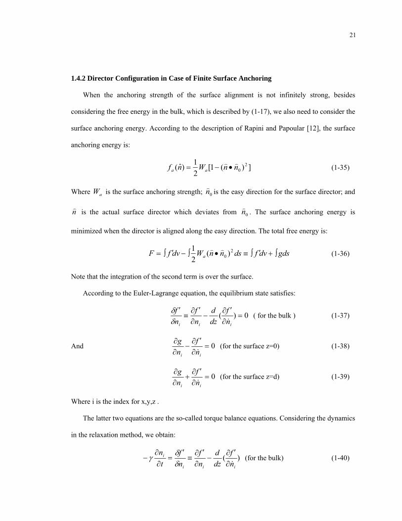
1.4.2 Director Configuration in Case of Finite Surface Anchoring
When the anchoring strength of the surface alignment is not infinitely strong, besides
considering the free energy in the bulk, which is described by (1-17), we also need to consider the
surface anchoring energy. According to the description of Rapini and Papoular [12], the surface
anchoring energy is:
])(1[21)ˆ( 2
0nnWnf aa)) •−= (1-35)
Where is the surface anchoring strength; aW 0n) is the easy direction for the surface director; and
n) is the actual surface director which deviates from 0n) . The surface anchoring energy is
minimized when the director is aligned along the easy direction. The total free energy is:
gdsdvfdsnnWdvfF a ∫+′∫≡•∫−′∫= 20 )(
21 )) (1-36)
Note that the integration of the second term is over the surface.
According to the Euler-Lagrange equation, the equilibrium state satisfies:
0)( =∂
′∂−
∂′∂
≡′
iii nf
dzd
nf
nf
&δδ
( for the bulk ) (1-37)
And 0=∂
′∂−
∂∂
ii nf
ng
& (for the surface z=0) (1-38)
0=∂
′∂+
∂∂
ii nf
ng
& (for the surface z=d) (1-39)
Where i is the index for x,y,z .
The latter two equations are the so-called torque balance equations. Considering the dynamics
in the relaxation method, we obtain:
)(iii
i
nf
dzd
nf
nf
tn
&∂′∂
−∂
′∂≡
′=
∂∂
−δδγ (for the bulk) (1-40)

22
And ii
is n
fng
tn
&∂′∂
−∂∂
=∂∂
− γ (for the surface z=0) (1-41)
ii
is n
fng
tn
&∂′∂
+∂∂
=∂∂
− γ (for the surface z=d) (1-42)
Where sγ is the viscosity constant of the surface.
-0.8
-0.6
-0.4
-0.2
0.0
0.2
0.4
0.6
0.8
1.0
Dire
ctor
Com
pon e
nt
0.0 0.1 0.2 0.3 0.4 0.5 0.6 0.7 0.8 0.9 1.0Normalized Thickness
nz
nx
ny
Fig.1.14. Director configuration of a chiral-doped homeotropic-alignment cell
with finite surface anchoring (no applied voltage).
Fig. 1.14 shows the calculated director configurations of a chiral-doped liquid crystal cell
with homeotropic surface alignment. The anchoring strength is . The other
parameters are: d/p = 0.6 , thickness d=5.0 μm, = 14.9 (pN), =7.9 , =15.2. Because the
surface anchoring strength is finite, the bulk twisting strength, which tends to tilt the director
away from the cell normal, is relatively stronger; the is decreased with the increase of surface
6100.8 −× 2/ mJ
11k 22k 33k
zn

23
anchoring energy. Fig.1.15 plots the component of the director through cells with different
surface anchoring strengths. The other parameters are the same as those parameters used in
Fig.1.14.
zn
0.0
0.1
0.2
0.3
0.4
0.5
0.6
0.7
0.8
0.9
1.0
z co
mpo
n ent
of d
irect
or-- n
z
0.0 0.1 0.2 0.3 0.4 0.5 0.6 0.7 0.8 0.9 1.0Normalized Thickness
Black: Wa = 5.0e-6 Blue: Wa = 7.0e-6 Red: Wa = 8.0e-6 Green: Wa = 1.0e-5
Fig.1.15. Z-component of the director of chiral-doped homeotropic-alignment cells at different
surface anchoring strengths.

CHAPTER 2
Light Propagation in Stratified Materials
2.1 Introduction
In classical electromagnetic theory, the state of light is described by two vectors, the electric
field Er
and the magnetic induction Br
. Light propagation is described by Maxwell's equations
[14].
0=
=
=
0=
B
D
jtDH
tBE
r
r
rr
r
rr
⋅∇
⋅∇∂∂
−×∇
∂∂
+×∇
ρ
(2-1)
where Dr
the electric flux density, Hr
the magnetic field strength, jr
the current density, and ρ
is the charge density. The properties of the medium through which the light is propagating are
also necessary to determine the field distribution:
,1=
,=
,=
BH
ED
Ej
rr
rr
rr
μ
ε
σ
(2-2)
where σ is the conductivity, ε the dielectric constant, and μ is the magnetic permeability. σ ,
ε and μ are tensors reflecting the properties of the materials and may depend on Er
and Br
. In a
dielectric medium, σ is negligible in most situations.
24

25
When discussing light propagation in dielectric media, we usually assume there is no source
in the media, i.e. no free charge ( 0=ρ ) and no free current ( ). 0=j
In a homogeneous and isotropic dielectric medium, the following equations are deduced from
Maxwell's equations:
0.=
0,=
2
22
2
22
tHH
tEE
∂∂
−∇
∂∂
−∇r
r
rr
εμ
εμ (2.3)
These are the standard wave equations with monochromatic plane wave solutions:
,=
,=)(
0
)(0
rkti
rkti
eHH
eEErr
rr
rr
rr
⋅−
⋅−
ω
ω
(2.4)
where is the wave vector and kr
ω is the angular frequency. The relationship between kr
and ω
is:
,==c
nkk ωr (2.5)
where εμ≡n is the refractive index. Both the electric field Er
and the magnetic field Hr
are
perpendicular to the propagation direction ( 0== 00 HkEkrr rr
⋅⋅ ), and are perpendicular to each
other. The phase velocity of light is described by:
.==nccv
εμ (2.6)

26
The dielectric constant )(= ωεε depends on the frequency of the electro-magnetic wave.
Therefore, electro-magnetic waves of a certain frequency propagate in a medium at their own
phase velocity, a phenomenon referred to as dispersion in optics.
When considering light propagation in liquid crystal devices, in most cases these materials
can be treated as stratified anisotropic materials. The basic idea is to divide a liquid crystal
device into many layers; if layer number is large enough, each layer is assumed to be optically
uniform. Two widely accepted methods, the Jones matrix method and Berreman's 4x4 method
[15] are introduced here.
2.2 Jones Matrix Method
In the Jones matrix method, the polarization state of light is described by a Jones vector
(2-7) ⎥⎦
⎤⎢⎣
⎡=
y
x
EE
Er
where , are the complex components of the electric field in the x, y directions,
respectively. The light is assumed to propagate along the z direction. As the amplitude and the
phase difference between the two components are consdered, so the vector is re-written as:
xE yE
⎥⎥⎦
⎤
⎢⎢⎣
⎡=⎥
⎦
⎤⎢⎣
⎡= φi
y
x
y
x
eEE
EE
Er
(2-8)
where φ = 2π( )d/λ is the phase difference of the o-light and the e-light. oe nn −
The light intensity is given by:
22
yx EEI += (2-9)
When light passes through a uniform birefrigent film, a Jones matrix, J, is used to describe
the optics of the system:

27
inout EJErr
= (2-10)
where inEr
, outEr
are the incident light and the transmitted light, respectively. For a non-absorbing
birefrigent film with a phase shift ϕ and in which the direction of the fast axis (along which
direction the refraction index is the smallest) makes an angle θ with respect to x-axis, the Jones
matrix is :
(2-11) )()()()( 1 θθθθ ϕϕ −== − RJRRJRJ
Where and . We may treat a nematic liquid crystal
cell as many birefrigent layers, so the total device can be represented by one Jones matrix
⎥⎦
⎤⎢⎣
⎡= ϕϕ ie
J0
01⎥⎦
⎤⎢⎣
⎡ −=
)cos()sin()sin()cos(
)(θθθθ
θR
totalJ
121... JJJJJ mmtotal •••= − (2-12)
x
y
xEyE
xnyn
zn
n
z
Fig.2.1 Local coordinate system - - z in the Jones matrix method. xE yE

28
The Jones vector of the output light can then be calculated:
(2-13) ⎥⎥⎦
⎤
⎢⎢⎣
⎡•=
⎥⎥⎦
⎤
⎢⎢⎣
⎡= in
y
inx
totalouty
outx
out EE
JEE
Er
In numerical computation, when the liquid crystal has a twist structure, it is convenient to
assume a local co-ordinate system, in which the axis is held to be the same as the in-plane
component of the director, and the axis is held in the x-y plane (Fig.2.1). It is important to
mention that the axis is perpendicular to the -z plane, so is orthogonal to the director.
xE
yE
yE xE yE
Suppose the director in the k layer is , the electric field in the local
electric field co-ordinate system of the k layer isthen:
),,(ˆ )()()()( kz
ky
kx
k nnnn =
⎥⎥⎦
⎤
⎢⎢⎣
⎡= )(
)()(
ky
kxk
out EE
Er
(2-14)
When light passes through the k+1 layer in which the director is
, the electric field in the local co-ordinate system of the k+1 layer
is:
),,(ˆ )1()1()1()1( ++++ = kz
ky
kx
k nnnn
(2-15) ⎥⎥⎦
⎤
⎢⎢⎣
⎡⎥⎦
⎤⎢⎣
⎡−⎥
⎦
⎤⎢⎣
⎡=
⎥⎥⎦
⎤
⎢⎢⎣
⎡= +
++
)(
)(
)1(
)1()1(
)cos()sin()sin()cos(
100
ky
kx
i
ky
kxk
out EEe
EE
Eθθθθϕr
where ϕ is the phase difference of the e-wave and the o-wave:
dnn oeff )(2−=
λπϕ (2-16)
and is the effective refractive index of the e-wave in the k+1 layer: effn
2)1(22)1(2
22
)(])(1[ ++ +−=
kze
kzo
eoeff
nnnn
nnn (2-17)

29
The Jones matrix method is a 2-by-2 matrix method; it is easy to be programmed and applied.
When considering the light propagating from one layer to another, reflection is not considered;
normally the Jones matrix method is not used to calculate reflectance.
2.3 Berreman's 4-by-4 Matrix Method
Berreman’s 4-by-4 matrix method was initially applied to liquid crystals in 1972 [15]. It is
based on the solution of Maxell’s equations without any significant approximations; it is an
accurate way to describe the optical properties for any medium as long as the medium can be
treated as a multi-layer structure and in each layer the optic axis is uniform. An isotropic media
layer is also treated the same way. Berreman’s 4-by-4 method has been extensively used in the
liquid crystal display (LCD) modeling, for the calculation of transmission, reflection, spectrum
and chromaticity, contrast-viewing angle and other optical properties. It is used in most
commercialized LCD modeling software.
In this method, a Cartesian-coordinate system is used in which the liquid crystal cell is in the
x-y plane. The dielectric tensor is assumed to be only a function of z. Considering an obliquely
incident light on a sample with a wave-vector k= ( ), the electric field
can be written as :
zyx kkk ,, )(0
→→⋅−= rktieEE ω
rr
)()(0 )( ykxktiykxktizik yxyxZ ezEeeEE −−−− ′== ωω rrr
(2-18)
Similarly the magnetic field is described by:
)()(0 )( ykxktiykxktizik yxyxZ ezHeeHH −−−− ′== ωω rrr
(2-19)
In order to make the fields dimensionless, we change variables such that:
0E
Eer
r= ,
0HHhr
r= ,
0kkkr
r=′ ,
0εε
ε ijij =′

30
After considering Maxwell’s equations:
EiHrr
ωε=×∇ (2-20)
HiErr
ωμ−=×∇ (2-21)
We obtain:
XAizX
k
rr
=∂∂
0
1 (2-22)
where And
⎥⎥⎥⎥⎥
⎦
⎤
⎢⎢⎢⎢⎢
⎣
⎡
=
y
x
y
x
hhee
Xr
A is the differential propagation matrix.
⎥⎥⎥⎥⎥⎥⎥⎥⎥⎥⎥
⎦
⎤
⎢⎢⎢⎢⎢⎢⎢⎢⎢⎢⎢
⎣
⎡
′′′
′
′′−⎟⎟
⎠
⎞⎜⎜⎝
⎛′
′′+′−′′−⎟
⎟⎠
⎞⎜⎜⎝
⎛′′
+′−′
′
′′−′
′′⎟⎟⎠
⎞⎜⎜⎝
⎛
′
′−′+′−⎟⎟
⎠
⎞⎜⎜⎝
⎛′
′′−′+′′
′
′′+
′
′−
′
′′
′
′′
−′′
′
′′−′
′′
′′′
=
zz
xxz
zz
yxz
zz
zyzxxyxy
zz
zxxxy
zz
xyz
zz
yyz
zz
zyyyx
zz
zxyzyxyx
zz
yx
zz
y
zz
yzy
zz
yzx
zz
x
zz
yx
zz
xzy
zz
xzx
kkkkk
kkkkk
kkkkk
kkkkk
A
εε
εε
εεε
εεε
ε
εε
εε
εε
εε
εεε
εεεε
εε
εεεε
εε
22
22
2
2
1
1
(2-23)
To simplify the equation, A is diagonalized to : SASA 1−=′ ; with 4 eigenvalues 1λ , 2λ
, 3λ , 4λ , which represent the forward and backward propagating ordinary and extra-ordinary
waves explicitly written as:
(2-24) 2/1201 )( m−= ελ
( 2/12
222 / eoftt
yx
tx mnn
mnεεεεελ −+
+= ) (2-25)
31
3λ = - 1λ (2-26)
( 2/12
224 / eoftt
yx
tx mnn
mnεεεεελ −−
+= ) (2-27)
The four associated eigenvector will be given as:
⎥⎥⎥⎥⎥
⎦
⎤
⎢⎢⎢⎢⎢
⎣
⎡
−−
−−
=
3,1
3,1
3,13,1
/
/))cos(sin(
1
λελ
λψ
yo
xz
zx
y
z
nnmn
mnnn
nar (2-28)
⎥⎥⎥⎥⎥⎥
⎦
⎤
⎢⎢⎢⎢⎢⎢
⎣
⎡
−−
−−
=
zx
y
y
o
zx
o
z
mnnn
n
mnnm
nar
4,2
4,2
4,22
4,2
)1(
))cos(sin(1
λλ
ελ
εψ (2-29)
where
e
z
o
zt nn
εε
ε 22 11
−+
= (2-30)
2
22
1 z
xtyof n
nn
−
+=
εεε (2-31)
))cos(()1( zo
tt narctgmm
εε
−= (2-32)
)sin(0
ix
kk
m θ== (2-33)
and where iθ is the angle of incidence in vacuum. A special case should to be mentioned is when
=1; then the four eigenvalues and the four eigenvectors cannot be used. They are instead
defined as:
zn

32
(2-34) 2/1201 )( m−= ελ
)1(2
2e
omε
ελ −= (2-35)
3λ = - 1λ (2-36)
4λ = - 2λ (2-37)
(2-38)
⎥⎥⎥⎥
⎦
⎤
⎢⎢⎢⎢
⎣
⎡
=
0
10
3,13,1 λ
ψ
(2-39)
⎥⎥⎥⎥
⎦
⎤
⎢⎢⎢⎢
⎣
⎡−
=
100
/4,2
4,2
oελ
ψ
The matrices S and are given by: 1−S
),,,( 4321 ψψψψ=S (2-40)
(2-41) MSNS T11 −− =
where is the transpose of S and TS
(2-42)
⎥⎥⎥⎥
⎦
⎤
⎢⎢⎢⎢
⎣
⎡
−−
=
0001001001001000
M
(2-43)
⎥⎥⎥⎥⎥
⎦
⎤
⎢⎢⎢⎢⎢
⎣
⎡
=
44
33
22
11
000000000000
ψψψψ
ψψψψ
MM
MM
N
T
T
T
T
33
Now, (2-43) becomes:
YAizY
kr
r
′=∂∂
0
1 (2-44)
Where XSYrr
1−= . This equation can be solved analytically by:
)()( 0 zYezzY zikrr r
ΛΔ=Δ+ (2-45)
So )()()( 10 zXSeSzzX zikrr r
−ΛΔ=Δ+ (2-46)
where (2-47)
⎥⎥⎥⎥⎥
⎦
⎤
⎢⎢⎢⎢⎢
⎣
⎡
=
Δ
Δ
Δ
Δ
ΛΔ
40
30
20
10
0
λ
λ
λ
λ
zik
zik
zik
zik
zik
eeee
er
In the numerical computation, we divide the sample into n slabs, each of which has a
thickness Δz, and Δz is small enough for the dielectric tensor in each slab to be treated as
constant. The fields that exit the surface are given by:
inout XbXrr
= (2-48)
111 )(*......*)( 00 −ΛΔ−ΛΔ= SeSSeSb zik
nzik
rr
(2-49)
We select a coordinate system in which the wave vector kr
is in the x-z plane, so . 0=yk
Considering a liquid crystal material whose director is ),,( zyx nnnn =) , then the dielectric
tensor is given by:
(2-50) jioeijoij nnnnn )( 222 −+=′ δε
Here , are the ordinary and extrordinary refraction indices if the material is a pure liquid
crystal.
on en

34
In order to meet the boundary conditions, considering the reflection of light, the field at the
input surface is:
riin XXXrrr
+= (2-51)
where is the incident field and iXr
rXr
is the reflected field at the input surface.
The transmited light is described by :
rit XbXbXrrr
+= (2-52)
The wave vector of the incident, reflected and transmitted waves are related as:
NNkkk iir
))rrr)(2 ⋅−= (2-53)
where N)
is the surface normal and it kkrr
= if the sample is surrounded by the same isotropic
medium at the input and the output surfaces.
The magnetic field components can be written in terms of the electric field, since
HitBE
rr
rωμ−=
∂∂
−=×∇ (2-54)
We have HEkrrr
ωμ=× (2-55)
Or hzhZ
ekrrr)
==×0
ωμ (2-56)
where 0
00 H
EZ = ,
HE
Z = and 0Z
Zz =
Similarly zehkrv)
=×− (2-57)
From (2-56) and (2-57), we can solve for and in terms of and . In general, xh yh xe ye

35
⎥⎥⎥⎥
⎦
⎤
⎢⎢⎢⎢
⎣
⎡
⎥⎥⎥⎥⎥⎥⎥
⎦
⎤
⎢⎢⎢⎢⎢⎢⎢
⎣
⎡
−
−−−=
⎥⎥⎥⎥⎥
⎦
⎤
⎢⎢⎢⎢⎢
⎣
⎡
00
001
001
00100001
2
2y
x
z
yx
z
y
z
x
z
yx
y
x
y
x
ee
zkkk
zkk
zkk
zkkk
hhee
(2-58)
Given an incident light field, the transmitted and reflected light fields are:
⎥⎥⎥⎥
⎦
⎤
⎢⎢⎢⎢
⎣
⎡
=
⎥⎥⎥⎥⎥
⎦
⎤
⎢⎢⎢⎢⎢
⎣
⎡
00iy
ix
iy
ix
iy
ix
ee
hhee
α ,
⎥⎥⎥⎥
⎦
⎤
⎢⎢⎢⎢
⎣
⎡
=
⎥⎥⎥⎥⎥
⎦
⎤
⎢⎢⎢⎢⎢
⎣
⎡
00ty
tx
ty
tx
ty
tx
ee
hhee
β and
⎥⎥⎥⎥⎥
⎦
⎤
⎢⎢⎢⎢⎢
⎣
⎡
=
⎥⎥⎥⎥⎥
⎦
⎤
⎢⎢⎢⎢⎢
⎣
⎡
ry
rx
ry
rx
ry
rx
ee
hhee
00
γ (2-59)
where
⎥⎥⎥⎥⎥⎥⎥
⎦
⎤
⎢⎢⎢⎢⎢⎢⎢
⎣
⎡
−
−−−=
001
001
00100001
2
2
izi
iyix
izi
iy
izi
ix
izi
iyix
kzkk
kzk
kzk
kzkk
α (2-60)
⎥⎥⎥⎥⎥⎥⎥
⎦
⎤
⎢⎢⎢⎢⎢⎢⎢
⎣
⎡
−
−−−=
001
001
00100001
2
2
tzt
tytx
tzt
ty
tzt
tx
tzt
tytx
kzkk
kzk
kzk
kzkk
β (2-61)
⎥⎥⎥⎥⎥⎥⎥
⎦
⎤
⎢⎢⎢⎢⎢⎢⎢
⎣
⎡
−
−−−=
rzr
ryrx
rzr
ry
rzr
rx
rzr
ryrx
kzkk
kzk
kzk
kzkk
2
2
100
100
10000100
γ (2-62)
From (2-58) we get:

36
⎥⎥⎥⎥⎥
⎦
⎤
⎢⎢⎢⎢⎢
⎣
⎡
+
⎥⎥⎥⎥
⎦
⎤
⎢⎢⎢⎢
⎣
⎡
=
⎥⎥⎥⎥
⎦
⎤
⎢⎢⎢⎢
⎣
⎡
ry
rx
iy
ix
ty
tx
ee
bee
bee
00
00
00
γαβ (2-63)
Noting
⎥⎥⎥⎥⎥
⎦
⎤
⎢⎢⎢⎢⎢
⎣
⎡
=
⎥⎥⎥⎥
⎦
⎤
⎢⎢⎢⎢
⎣
⎡
ry
rx
ty
tx
ty
tx
eeee
ee
ββ
00
and
⎥⎥⎥⎥⎥
⎦
⎤
⎢⎢⎢⎢⎢
⎣
⎡
=
⎥⎥⎥⎥⎥
⎦
⎤
⎢⎢⎢⎢⎢
⎣
⎡
ry
rx
ty
tx
ry
rx
eeee
ee
γγ00
,
We have
⎥⎥⎥⎥
⎦
⎤
⎢⎢⎢⎢
⎣
⎡
=
⎥⎥⎥⎥⎥
⎦
⎤
⎢⎢⎢⎢⎢
⎣
⎡
−
00
)( iy
ix
ry
rx
ty
tx
ee
b
eeee
b αγβ (2-64)
So,
⎥⎥⎥⎥
⎦
⎤
⎢⎢⎢⎢
⎣
⎡
−=
⎥⎥⎥⎥⎥
⎦
⎤
⎢⎢⎢⎢⎢
⎣
⎡
−
00
)( 1 iy
ix
ry
rx
ty
tx
ee
bb
eeee
αγβ (2-65)
Now, from (2-65), we can calculate both the trasmitted and the reflected electric field, and the
magnetic field will also be calculated. The light intensities of both the transmitted and reflected
light will be known.
Fig.2.2 shows the transmittances of circularly-polarized light from two cholesteric liquid
crystal cells. For the cell whose twist sense is identical to the handedness of the circularly-
polarized light, there is a reflection band with a band width of ( - )p and a reflection
wavelength center at ( + )p/2. The parameters used here are: thickness d = 6.0 μm, pretilt
angle
en on
en on
pθ =0°, d/p ratio = 15, elastic constant: = 15.5 (PN), =14.0 , =28.0,
=1.5, =1.7. The entrance and exit media are air (n=1).
11k 22k 33k
on en

37
0
10
20
30
40
50
60
70
80
90
100
Tran
smitt
a nce
( %
)
500 550 600 650 700 750 800Wavelength (nm )
Fig. 2.2. Spectral response of clock-wise circularly-polarized light from two cholesteric cells.
Black: twist sense of the cell is clockwise; Red: twist sense of the cell is counter-clockwise
2.4 Light Propagation in Periodic Media
2.4.1 Introduction to Grating
Gratings are periodic media that have been widely used in optical applications. A grating can
fall into one of two categories: an amplitude grating, which spatially modulates the intensity of
light, and a phase grating, which spatially modulate the phase of light. The latter can be realized
by periodically modulating the thickness or the refractive index of a medium, as in holographic
polymer dispersed liquid crystals (HPDLC), which are the focus of our research.
In a periodic medium, the refractive index exhibits a translational symmetry:

38
),(=)( arnrn rrr+ (2-66)
where ar is a constant vector. For a one dimensional phase grating, the refractive index satisfies
)(=)( Λ+ mznzn , where is an integer and m Λ is the period of the grating, or pitch. The
refractive index can be expanded in a Fourier series:
.2cos=)(1=
0 ⎟⎠⎞
⎜⎝⎛
Λ+ ∑
∞ zmnnzn mm
π (2-67)
θ θ
Λ
x
z
ik
dkθθ
2ksin(θ)
Fig. 2.3. Diffraction of a monochromatic plane wave by an optically thick grating.
kkk di ==rr
. The component of momentum perpendicular to the grating vector kr
is
conserved.
The simplest case is a sinusoidal grating, where only and the first Fourier component are
non-zero:
0n

39
.2cos=)( 10 ⎟⎠⎞
⎜⎝⎛
Λ+
znnzn π (2-68)
Consider the monochromatic wave diffracted from a periodic medium: the index modulation
is lumped to an array of planes separated by equal distance, as illustrated in Fig. 2.3. Assuming
that the number of planes is infinite, the reflections from these planes are specular. The path
difference for rays reflected from adjacent planes is θsin2Λ , where θ is the angle between the
incident beam and the grating planes. The interference is constructive when the phase difference
for neighboring reflected rays is an integer multiple of π2 , which leads to Bragg's law:
0
=sin2n
N λθΛ (2-69)
where is an integer, and is the average refractive index of the medium. The angle N 0n θ
satisfying (2-69) is defined as the Bragg angle.
In space, the grating period is represented by the grating vector , where k−k kr
Λ≡ /2= πkr
is known as the grating wave number. Bragg's law becomes kNkk ri
rrr=+ , and is a vector in
the (one-dimensional) reciprocal lattice. The component of the momentum perpendicular to the
grating vector k is conserved.
kNr
r
In a thin grating, as depicted in Fig. 2.4, the transverse dimension of the periodic medium is
relatively small compared to the beam size and/or the wavelength. Due to the finite size of the
grating planes, the diffraction from each plane should be considered in addition to the specular
reflection. Constructive interference also occurs in directions other than the specular reflection
direction. The condition for constructive interference is:
)./(=sinsin nN λθθ ′Λ+Λ (2-70)

40
A dimensionless parameter (Klein-Cook parameter), is introduced to
qualitatively define thick or thin gratings, where is the thickness of the grating. When ,
the grating is classified as a thick grating, and when
20/2 Λ≡ nLQ πλ
L 1>>Q
1<<Q , the grating is classified as a thin
grating.
θ θ'
Λ
x
z
Fig. 2.4. Diffraction of a monochromatic plane wave by an optically thin grating. θ may not be
equal to θ ′ .
2.4.2 Coupled Wave Theory [16]
Coupled wave theory was introduced by Kogelnik in 1969 to treat thick dielectric gratings
( ) [17]. In this approach, the refraction index profile was assumed to be sinusoidal and the
dielectric medium is isotropic. The light propagating in the periodic medium is assumed to be
polarized light and the diffracted light is coupled with the incident beam. Coupled wave theory is
known for its simplicity and versatility to theoretically simulate grating diffraction phenomena.
1>>Q
Let us consider the light propagation in a one-dimensional periodic medium with a sinusoidal
index modulation described by (2-68). Assume: (1) plane waves have uniform amplitudes; (2) the
grating extends laterally to infinity ( , thick grating); and (3) the electric fields of both the 1>>Q

41
incident light and the diffracted light are parallel to the grating planes and perpendicular to the
grating vector, as in Fig. 2.5. In other words, only the transverse electric (TE) mode is discussed.
Based on these three assumptions, the electric field of the incident and diffracted beams can be
written as:
[ ] [ ])(exp)(exp= 2211 rktiArktiAE rrrr⋅−+⋅− ωω (2-71)
where 1kr
and 2kr
are the wave vectors, and are the amplitudes of the electric fields, and 1A 2A
ω is the frequency of the beams. The wave vectors and the frequency of the light are connected
by: cnkk /|=|=|| 021 ωrr
. When the zx − plane is set as the plane of incidence, the wave vectors
can then be written in Cartesian coordinates: ),0,(= 111 βαkr
and ),0,(= 222 βαkr
. Therefore, the
electric field is:
[ ] [ ].)(exp)(exp= 222111 zxtiAzxtiAE βαωβαω −−+−− (2-72)
0 L
θ1 θ2
θ1 θ2
0
L x
z
y x
z
y
(a) Transmission grating (b) Reflection grating
Fig. 2.5. Diffraction by optically thick gratings. (a) Transmission grating; (b) Reflection grating.

42
The electric field satisfies the wave equation:
0,=)( 22
22 En
cω
+∇ (2-73)
where is the refractive index of the medium. n
2.4.3. Coupled Wave Theory for Transmission Gratings
For a transmission grating with infinite dimension in the direction, the amplitudes of the
electric fields are functions of
z
x only. In a medium with a sinusoidal index modulation, as
described in (2-68), the wave equation of the electric field can be represented by:
( )[ ]
( )[ ]
( )[ ].exp
expcos2=
exp2
1,2=
212
2
1,2=102
2
2
2
1,2=
zxtiAnc
zxtiAKznnc
zxtiAdxdi
dxd
jjjj
jjjj
jjjjj
βαωω
βαωω
βαωα
−−−
−−−
−−⎥⎦
⎤⎢⎣
⎡⎟⎟⎠
⎞⎜⎜⎝
⎛−
∑
∑
∑
(2-74)
The term is neglected because is usually of the order of to . Assuming the
energy interchange between the transmitted wave and the reflected wave is slow (i.e., and
are slowly varying functions), the second order derivatives of and are neglected. (2-74)
becomes:
21n 1n 110− 310−
1A 2A
1A 2A
( ) ( )
( ) ( )[ ] ( )
( )].exp
exp[expexp=
exp2exp2
222
111102
2
222
2111
1
zixiA
zixiAiKziKznnc
zixidxdAizixi
dxdAi
βα
βαω
βααβαα
−−+
−−+−−
−−−−−−
(2-75)
By multiplying (2-75) with )(exp zixi jj βα −− , with or , and integrating over ,
two first order differential equations are obtained:
1=j 2 z

43
,=
,=
1212
2121
xi
xi
eAidxdA
eAidxdA
α
α
κ
κ
Δ
Δ−
−
− (2-76)
where:
( ),coscos2==
,cos
=,cos
=
12021
2
121
1
112
θθλπααα
θλπκ
θλπκ
−−Δ n
nn
(2-77)
and the following condition is satisfied:
.= 12 K±ββ (2-78)
K
x
z Δα
K
x
z
k1
k2
k1
k2
(a) Δα = 0, phase matched (b) Δα ≠ 0, phase mismatch
Fig. 2.6. K-space of transmission gratings (a) Ideal phase match 0=αΔ ; (b) not ideal phase
match 0≠Δα .
The phase mismatch αΔ determines the coupling and energy exchange between the beams.
When 12 cos=cos θθ , 0=αΔ , there is an ideal phase match, as shown in Fig. 2.6. The trivial
solution 12 = θθ corresponds to the transmitted beam; the non-trivial solution
12 = θθ − corresponds to the diffracted beam. The Bragg condition is satisfied when 0=αΔ :

44
,2
arcsin==0
21 Bnθλθθ ≡⎟⎟
⎠
⎞⎜⎜⎝
⎛Λ
±− (2-79)
where Bθ is known as the Bragg angle, and the wave equation becomes:
,=,= 12
21 Ai
dxdAAi
dxdA κκ −− (2-80)
where: .cos
= 1
B
nθλ
πκ (2-81)
The solutions to (2-80) are:
( ) ( ) ( )( ) ( ) ( ) ,sin0cos0=
,sin0cos0=
122
211
xiAxAxAxiAxAxA
κκκκ
−−
where and are the electric field amplitudes of the incident beam and the diffracted
beam at the incident surface. For a single incident beam (
( )01A ( )02A
( ) 0=02A ), the solutions become:
( ) ( ) ( ) ( ) .sin0=,cos0= 1211 xiAxAxAxA κκ − (2-82)
Energy is conserved in this solution. The diffraction efficiency of the grating is:
( )( )
,sin=0
== 22
1
22 L
A
LAII
incident
diffracted κη (2-83)
where is the thickness of the cell. For the ideal gratings in which all of our assumptions are
satisfied, the diffraction efficiency reaches its first maximum when
L
/2= πκL . When /2> πκL
(over-modulation), the diffraction efficiency decreases.

45
Δα
K
x
z
k1
k2
K
Δα
K
x
z
k1
k2
(a) (b)
Fig. 2.7. Phase mismatch in transmission gratings due to (a) angular deviation; and (b)
wavelength deviation.
When the incident angle deviates slightly from the Bragg angle, θθθ Δ+− B=1 , the
diffraction angle determined by (2-78) is:
.=2 θθθ Δ+B (2-84)
The deviation from the Bragg angle results in a phase mismatch given by:
,=sin2= θθθα Δ−Δ−Δ Kk B (2-85)
where λπ /2= 0nk , as illustrated in Fig. 2.7(a). For the mismatched case, solutions to the
coupled wave equation (2-76) are:
( ) ( ) ,cossin22
exp0= 11 ⎥⎦⎤
⎢⎣⎡ +
Δ⎟⎠⎞
⎜⎝⎛ Δ
− sxsxs
ixiAxA αα
( ) ( ) ,sin2
exp0= 2112 sx
sxiiAxA κα
⎟⎠⎞
⎜⎝⎛ Δ
−
where .2
=2
22 ⎟⎠⎞
⎜⎝⎛ Δ
+ακs (2-86)

46
The corresponding diffraction efficiency is:
( )( )
.2
1sin
2
=cos0cos
=1/22
22
2
2
12
1
22
2
⎪⎭
⎪⎬⎫
⎪⎩
⎪⎨⎧
⎥⎥⎦
⎤
⎢⎢⎣
⎡⎟⎠⎞
⎜⎝⎛ Δ
+
⎟⎠⎞
⎜⎝⎛ Δ
+κακ
ακ
κθθ
η LA
LA (2-87)
The diffraction efficiency decreases with an increase of phase mismatch, as illustrated in Fig. 2.8.
The angular dependence of the diffraction efficiency can be derived from (2-87). The diffraction
efficiency drops to 1/2 when the deviation of the incident angle from the Bragg angle is:
.=2== 1/2 πκκθθ Λ
ΔΔK
(2-88)
0
0.1
0.2
0.3
0.4
0.50.6
0.7
0.8
0.9
1
-10 -8 -6 -4 -2 0 2 4 6 8 10
Phase Mismatch
Diffr
actio
n Ef
ficie
ncy
Fig. 2.8. The diffraction efficiency decreases with the increase of phase mismatch. Red: kL=2π/3,
Black: kL=π/2. Phase Mismatch: Δα/2k.
A deviation in wavelength, λΔ , can also lead to a phase mismatch, as shown in Fig. 2.7 (b). The
phase mismatch is given by:

47
.cos
=0 Bn θ
λπαΛ
ΔΛ
−Δ (2-89)
The diffraction efficiency decreases to half the maximum value when the wavelength of incident
beam changes by:
.cos2= 021 Bn θ
πκλ Λ
ΛΔ (2-90)
Therefore, 21λΔ can represent the spectral bandwidth. Fig. 2.9 plots the diffraction efficiency as a
function of the phase mismatch for different cell thicknesses.
The above discussion is valid for TE waves. For more general cases, the electric field is a
vector field, and the dielectric constant is a tensor field. The periodic medium is described by
( )rk rr⋅+′ cos= 1εεε (2-91)
where ε is the average dielectric tensor, and 1ε is the tensor representing the amplitude of the
periodic dielectric modulation. Following the same procedures, the coupled wave equations can
be derived, which have the same form as those of the TE wave (2-76), but with different coupling
constants:
;
cos2=
,cos2
=
112022
21
211011
12
ppn
ppn
rr
rr
εεθλ
πκ
εεθλ
πκ
⋅
⋅ (2-92)
and αΔ is given by:
.= 12 xK±−Δ ααα (2-93)
xK is the x component of the grating vector kr
; and and are the refractive indices
associated with
1n 2n
( )[ ]rktip rrr⋅− 11 exp ω and ( )[ ]rktip rrs
⋅− 22 exp ω , respectively.

48
0
0.10.2
0.3
0.4
0.50.6
0.7
0.80.9
1
-1 -0.5 0 0.5 1
Phase Mismatch
Diff
ract
ion
Effic
ienc
y
kL=1.0kL=1.5kl=2.0kL=2.5
Fig. 2.9. Diffraction efficiency as a function of phase mismatch (Δβ/2k) for reflection gratings
with different thicknesses kL.
The diffraction efficiency is obtained following the same approach for TE waves. In the case
of TM waves, the coupling constant is given by Θcosp κκ = , where Θ is the angle between the
electric fields of the incident beam and the diffracted beam [17]. The diffraction efficiency of the
TM wave has the same form as the TE wave, but with a smaller coupling constant.
2.4.4. Coupled Wave Theory for Reflection Gratings
For reflection gratings, the boundary conditions require that 21 = αα (i.e., 21 = θθ − ), and
that the amplitude of both the incident and reflected beams be functions of only. The coupled
wave equation for reflection gratings is deduced by following a similar approach to that of
transmission gratings:
z

49
zi
zi
eAidz
dA
eAidz
dA
β
β
κ
κ
Δ
Δ−−
12
21
=
= (2-94)
where: ,= 12 K±−Δ βββ (2-95)
and: .sin
=1
1
θλπκ n
(2-96)
The diffraction efficiency of a reflection grating is derived by solving (2-94). In the case of a
perfect phase match ( 0=βΔ ), the diffraction efficiency is:
.tanh= 2 Lκη (2-97)
Similar to the case of transmission gratings, the coupling constant of the TM wave in a
reflection grating is given by Θcosp κκ = , where Θ is the angle between the electric fields of
the incident beam and the diffracted beam. The diffraction efficiency of the TM wave is always
less than that of the TE wave for reflection gratings.
Deviation from the Bragg condition results in a phase mismatch ( 0≠Δβ ) given by:
,sin42= 10 θλππβ n−
ΛΔ (2-98)
when 0>1θ , the diffraction efficiency of a reflection grating with a phase mismatch is:
,
sinh2cosh
sinh=2
222
22
sLsLs
sL
⎟⎠⎞
⎜⎝⎛ Δ
+β
κη (2-99)
where: .2
=2
22 ⎟⎠⎞
⎜⎝⎛ Δ
−βκs (2-100)
Diffraction efficiency as a function of phase mismatch is illustrated in Fig. 2.10.
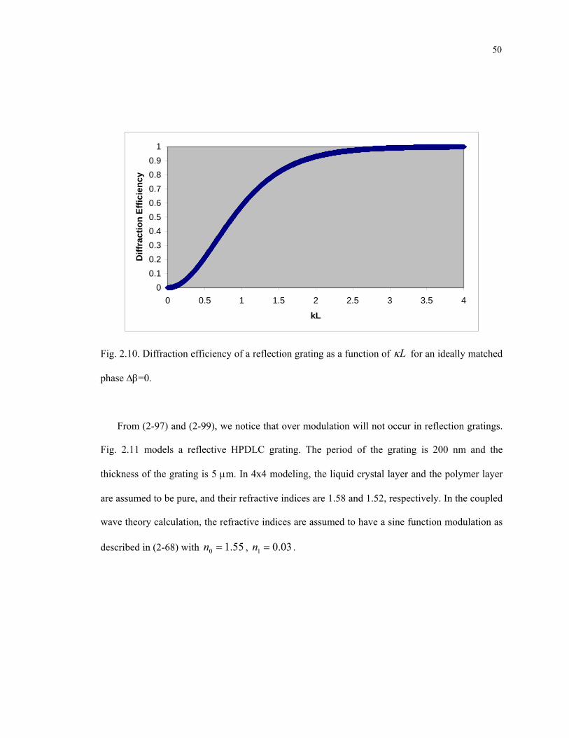
50
00.10.20.30.40.50.60.70.80.9
1
0 0.5 1 1.5 2 2.5 3 3.5 4
kL
Diff
ract
ion
Effic
ienc
y
Fig. 2.10. Diffraction efficiency of a reflection grating as a function of Lκ for an ideally matched
phase Δβ=0.
From (2-97) and (2-99), we notice that over modulation will not occur in reflection gratings.
Fig. 2.11 models a reflective HPDLC grating. The period of the grating is 200 nm and the
thickness of the grating is 5 μm. In 4x4 modeling, the liquid crystal layer and the polymer layer
are assumed to be pure, and their refractive indices are 1.58 and 1.52, respectively. In the coupled
wave theory calculation, the refractive indices are assumed to have a sine function modulation as
described in (2-68) with , 55.10 =n 03.01 =n .

51
Modeling of Reflection Grating
0
0.1
0.2
0.3
0.4
0.5
0.6
0.7
500 550 600 650 700 750 800
Wavelength ( nm )
Ref
lect
ion
4x4 modelingcoupled wave theory
Fig. 2.11. Modeling of reflection grating at normal incidence. Berreman’s 4x4 method and
coupled wave theory calculation are compared.
2.5 Summary
In this chapter, we have investigated light propagation in stratified materials. Based on
Maxwell’s equations, both the Jones matrix and Berreman’s 4x4 method are discussed and
modeling was given to explain the grating effect of a cholesteric and HPDLC cells. Furthermore,
coupled wave theory was discussed with a focus on explaining diffraction by one-dimensional
transmission and reflection mode phase gratings. The effects of various factors on diffraction
efficiency were mathematically investigated. While only isotropic gratings are discussed in detail,
the anisotropic gratings can also be treated with a similar method. The results of this chapter can
be applied to the HPDLC gratings, which can be approximated as phase gratings.

CHAPTER 3
Holographic Polymer Dispersed Liquid Crystal
3.1 Introduction to Holography
In conventional photography, only the distribution of light intensity of the object is recorded
and reconstructed. As nature of light and its application are further researched, the idea of
recording the complete wave field, both the phase and the amplitude of light, is inspired.
Reconstructing the same wave front from a hologram reproduces the image of the object. Since
most recording media respond only to the intensity of light, the phase information is transformed
into intensity during a holographic recording by the interference of monochromatic coherent
light. So, in definition, a hologram is the recording of the interference pattern of multiple beams
where the recording medium is positioned.
The interference of coherent light rays can be described by the superposition of the electric
fields: . The holographic recording time is usually much longer than the period of
the light. The average light intensity over a period is
tij
N
jeEE ω−∑
rr
1==
( ) ( ) ( )( ) ( ) ( ),21=
1=1=
* rErErErErI ml
N
m
N
l
rrrrrrrrr ∑∑⋅∝ where ( )rI r is the spatial distribution of the light
intensity, ( )rE rr the spatial distribution of the electric field, and ( )rEl
rr and ( )rEm
rr are the electric
field components of the different recording beams.
The first holograms were demonstrated by Gabor in 1948 [18,19]. In Gabor's in-line
holography setup, the interference pattern was generated by both the transmitted beam passing
through the object and the scattered light, as shown in Fig. 3.1. Gabor’s holography setup is only
52

53
applicable to objects with high transmittance and the hologram is usually weak; two
superimposed, out-of-focus twin images could be observed.
point source
object
recordingmedium
hologramvirtual image
real image
(a) (b)
Fig. 3.1 Optical setup for recording (a) and reconstructing (b) in-line hologram.
object beam
referencebeam
recordingmedium
referencebeam
hologram
virtualimage
realimage
(a) (b)
Fig. 3.2. The optical setup for recording (a) and reconstructing (b) off-line hologram.

54
Off-axis holography was introduced by Leith and Upatnieks in 1962 [20], as illustrated in
Fig. 3.2. In off-axis holography, the reference beam is separated from the illumination beam and
is directed to the photographic plate at an angle with the object beam. When reconstructed, the
real image and the virtual image are both located off the direct transmitted beam and are widely
separated from each other. The image quality of the hologram can be improved by adjusting the
intensity of both beams to increase the contrast ratio in the interference pattern.
3.2 Introduction to Holographic Polymer Dispersed Liquid Crystals
Holographic polymer dispersed liquid crystals (HPDLCs) are the successors of traditional
polymer dispersed liquid crystals (PDLC) that are comprised of a rigid polymer matrix, and
randomly dispersed liquid crystal droplets inside the polymer matrix. Usually HPDLCs have a
stratified structure with alternating layers of liquid crystal rich and polymer rich planes, formed
by the holographic exposure of a mixture of liquid crystals and photo-polymerizable monomers.
HPDLCs are normally treated as switchable phase gratings. The first switchable grating based
on a PDLC was introduced by Margerum and co-workers at Hughes Research Labs in 1988 [ 21].
A periodically modulated distribution of the liquid crystal droplet density in the polymer network
was generated under a masked UV exposure of the UV-curable PDLC mixture, the periodic index
modulation in the PDLC film functioned as a transmission grating that could be deactivated by
the realignment of the liquid crystal molecules in the LC droplets under the external electrical
field. The first switchable PDLC transmission grating formed by holographic exposure was
developed by Sutherland and co-workers in 1993 [22]. The prepolymer mixture was cured in the
visible wavelength range. The first HPDLC reflection grating was reported by Tanaka and co-
workers [23]. HPDLCs have found applications in displays [24, 25, 26] and optical
telecommunication [27] with their switchability and their relatively simple fabrication process.

55
To fabricate a conventional HPDLC cell, two ITO glass substrates with anti-reflection (AR)
coatings are assembled with uniforly spread spacers to control the cell gap. The recording
medium, or PDLC mixture is sandwiched between these ITO glass substrates. The cell is exposed
to the interference pattern generated by two monochromatic coherent laser beams generally
carrying equal powers and polarizations. The light induces a phase separation during the photo
polymerization of the monomers in the mixture and causes the liquid crystals to be phase
separated into randomly oriented droplets in this process. On the other hand, as the lights create
regions of complete constructive and destructive interference, the photo polymerization in the
bright (constructive) area is faster than in the dark (destructive) region; the liquid crystals diffuse
to the dark region and the monomers to the bright region. Finally, a spatially periodic distribution
of polymer and liquid crystal (LC) droplets is generated. The average refractive index of the LC
droplets, thus the refractive index difference between the LC rich region and polymer rich region,
can be changed with a realignment of the liquid crystal molecules by an external electric field. In
a normal mode HPDLC, refractive indices of the polymer and the LC droplet are unmatched
without an external field, while in the reverse mode, the refractive indices of the polymer and the
LC droplets are matched without an external field. In either case, an external electric field can
switch the HPDLC from a holographic state to a non-holographic state and Vice Versa.
The interference of two collimated laser beams is utilized to generate the interference pattern
for the holographic exposure. The interference pattern of the two coherent monochromatic beams
has the form:
( ) ( )[ ]0212121 coscos2= φθ +⋅−++ rkkIIIIrI rrrr (3-1)
where and are the beam intensities; θ is the angle between the polarization direction of the
recording beams;
1I 2I
1kr
and 2kr
are the wave vectors of the recording beams; and 0φ is the phase
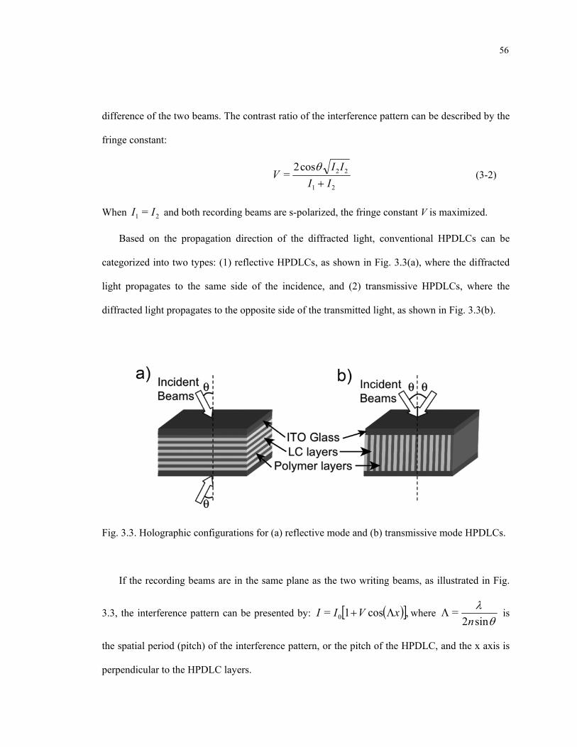
56
difference of the two beams. The contrast ratio of the interference pattern can be described by the
fringe constant:
21
22cos2=
IIII
V+θ
(3-2)
When and both recording beams are s-polarized, the fringe constant V is maximized. 21 = II
Based on the propagation direction of the diffracted light, conventional HPDLCs can be
categorized into two types: (1) reflective HPDLCs, as shown in Fig. 3.3(a), where the diffracted
light propagates to the same side of the incidence, and (2) transmissive HPDLCs, where the
diffracted light propagates to the opposite side of the transmitted light, as shown in Fig. 3.3(b).
Fig. 3.3. Holographic configurations for (a) reflective mode and (b) transmissive mode HPDLCs.
If the recording beams are in the same plane as the two writing beams, as illustrated in Fig.
3.3, the interference pattern can be presented by: ( )[ ],cos1= 0 xVII Λ+ where θ
λsin2
=n
Λ is
the spatial period (pitch) of the interference pattern, or the pitch of the HPDLC, and the x axis is
perpendicular to the HPDLC layers.

57
3.3 Transmission Mode HPDLCs
The conventional transmission mode HPDLCs have grating planes oriented perpendicular to
the cell surfaces. The interference pattern is generated by two coherent laser beams incident from
the same side of the cell, as illustrated in Fig. 3.3(b); a stratified structure of polymer rich and
liquid crystal rich layers is formed by the exposure. The pitch of the grating is determined by:
ww
w
n θλsin2
=Λ (3-3)
where wθ is the incident angle inside the HPDLC, wλ is the recording beam wavelength, and
is the refractive index at
wn
wλ . The wavelength reflected by the grating is:
ww
rrwrrr
wiw
rirwrrirr n
nnnn
nnnθθλθ
θθλθλ
sinsinsin2
coscos=cos2= =Λ=Λ
where is the refractive index of the HPDLC at the reading beam wavelength rn rλ , riθ is the
reading beam incident angle inside the HPDLC, and rθ is the angle between the incident (or
diffracted) beam and the grating planes. The diffraction properties highly depend on the
difference between the refractive index of the polymer rich layer and the liquid crystal rich layer.
Fig. 3.4 is a schematic illustration of the operation principle of transmission mode HPDLCs. In
the field-off state, light is strongly diffracted by the grating; while in the field-on state, light
passes through as the grating is deactivated by the electric field.
The polarization dependence of the diffraction efficiency of transmission gratings was first
revealed by Sutherland and co-workers. Their research showed that the coupling coefficient for
the TE wave (s-polarization) and the TM wave (p-polarization) are different and the index
modulation of the TM wave was larger than that of the TE wave [22], which indicated that the
orientation of LC droplets has a preferred direction perpendicular to the grating planes.
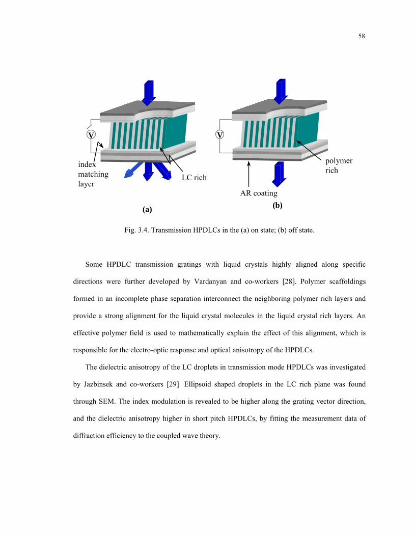
58
polymerrich
index matching layer
V
(a)
LC rich
V
(b)AR coating
Fig. 3.4. Transmission HPDLCs in the (a) on state; (b) off state.
Some HPDLC transmission gratings with liquid crystals highly aligned along specific
directions were further developed by Vardanyan and co-workers [28]. Polymer scaffoldings
formed in an incomplete phase separation interconnect the neighboring polymer rich layers and
provide a strong alignment for the liquid crystal molecules in the liquid crystal rich layers. An
effective polymer field is used to mathematically explain the effect of this alignment, which is
responsible for the electro-optic response and optical anisotropy of the HPDLCs.
The dielectric anisotropy of the LC droplets in transmission mode HPDLCs was investigated
by Jazbinsek and co-workers [29]. Ellipsoid shaped droplets in the LC rich plane was found
through SEM. The index modulation is revealed to be higher along the grating vector direction,
and the dielectric anisotropy higher in short pitch HPDLCs, by fitting the measurement data of
diffraction efficiency to the coupled wave theory.

59
s p
p s(a)
G1
G2
PR
Fig. 3.5. Polarization independent electro-optical device based on stacking two polarization
sensitive transmission mode HPDLCs (G1 and G2) and a polarization rotator (PR). Courtesy of
Boiko and co-workers [30].
A polarization insensitive HPDLC device was developed by Boiko and co-workers [30] using
two identical transmission HPDLCs with a polarization rotator in between, as illustrated in Fig.
3.5. The polarization rotator fabricated from reactive mesogen film can rotate the polarization of
certain wavelength of light by /2π , thus the s-polarized light traveling through the first HPDLC is
transformed to p-polarized light by the polarization rotator and is then diffracted by the second
HPDLC, while the p-polarized light diffracted by the first HPDLC is transformed to s-polarized
light and then passed through the second HPDLC. The contrast ratio of the diffraction efficiencies
of p-polarization and s-polarization of the single transmission HPDLC in this device is high (~30)
at 1550 nm. The diffraction efficiency of the stacked device is as high as for non-polarized
light. An SEM photograph of a transmission mode HPDLC operating at ~ 1500 nm is illustrated
in Fig. 3.6.
98%

60
Fig..3.6. The SEM photograph of a transmission mode HPDLC operating at 1500 nm. The top
substrate is pealed before the SEM image is captured.
3.4 Reflection Mode HPDLC
Reflection mode HPDLCs are recorded by laser beams incident from different sides of the
cell, as illustrated in Fig. 3.3(a). When the two recording beams are symmetric, the periodic
interference pattern is along the cell normal direction and the resulting grating planes are parallel
to the cell surfaces.
Unlike the transmission mode HPDLCs, the LC droplets in reflective HPDLCs are assumed
to be randomly oriented in the plane parallel to the cell surface, since normally no polarization
dependence of reflection efficiency is identified in reflective HPDLCs. Consequently, the average
refractive index of the LC droplets is given by:
3
2=22eo
LCnnn +
(3-4)

61
Fig. 3.7. The SEM photograph of a reflective HPDLC operating at ~1500 nm. The image is of the
cross section of the cell.
However, as the result of an incomplete phase separation, there are still liquid crystals in the
polymer rich layer, and the polymer networks extends into the LC rich layer. Therefore, the
average refractive index of both the polymer rich region, pn , and the LC rich region, ,LCn are in
the range defined by and (the refractive index of the polymer). The index modulation LCn pn
pLC nnn −≡1 is less than , and is typically in the order of . pLC nn − 210−
For liquid crystals with a positive dielectric anisotropy ( 0>εΔ ), when and the LC
molecules are aligned parallel to the applied electric field, the HPDLC cell will appear
transparent to the reading light. Fig. 3.7 is a SEM photograph of the polymer network of a
reflective HPDLC operating at around 1500 nm. The SEM image was taken after the liquid
crystals were washed away. The stratified polymer network and cavities that used to be occupied
by the liquid crystal are clearly identified.
po nn ≈

62
3.5 Variable-Wavelength HPDLC
So far most HPDLC related electro-optical devices function as an electrically switchable
grating with two states; the grating state (or switch-off state) without an external electric field and
transparent state (or switch-on state) with an applied external electric field. Recently, a variable-
wavelength switchable Bragg grating formed in polymer-dispersed liquid crystals was presented
by the Display and Photonics Laboratory of Brown University [31].
This innovative device can switch between two distinctly different reflecting states. A
blended monomer system was prepared by mixing Ebecryl 4866 with Ebecryl 8301 (both from
UCB Radcure) in a ratio of 2:1. This was then mixed with the liquid crystal BL038 (EM
Industries) with a weight ratio of 50:36:14 for the monomers: liquid crystal : photoinitiator
solutions, respectively. This was homogenized and mixed with a Tergitor Min-Foam 1X
surfactant from Union Carbide(3 wt%). The mixture was sensitized with a Rose Bengal and N-
Phenylglycine in 1-vinyl-2-pyrrolidone photoinitiator so that the polymerization could be carried
out in the visible wavelength range with an Ar laser. A cell was formed by drop filling this
mixture between ITO-coated glasses. 5 μm spacers were used to control the cell gap.
+
In the zero field state (Fig. 3.8(a)), the average index of the liquid crystal layer is
greater than that of the polymer layer and a reflection peak is observed since < . As
the field is increased as shown in Fig. 3.8(b), the partial alignment of the liquid crystal droplet
reaches a condition where ~ , and no reflection is observed because the layers are
index matched and optically homogeneous. At higher electric fields, as shown in Fig. 3.8 (c), the
liquid crystal becomes highly aligned and decreases to a value below , the sample
reflects again at a different wavelength. Fig. 3.9(a) shows a plot of peak wavelength and
reflectance as a function of applied voltage. Reflectance is normalized to the zero-voltage value.
)(2 Enl
1ln 1ln )(2 Enl
1ln )(2 Enl
)(2 Enl 1ln

63
The wavelength span is from a zero-voltage value of 450 nm to a minimum of 438 nm in the
switched state. Fig. 3.9(b) shows the experimentally measured reflectance spectrum at the zero-
voltage state, the index-matched state (120 V), and the switched state (220 V).
Fig. 3.8. Schematic illustration of a reflecting variable-wavelength HPDLC. (a) The average index of the liquid crystal layer is greater than that of the polymer layer ; (b) As
the field is applied, ~ , and the index grating is erased and the sample is optically
homogeneous; (c) The further increased field generates the highly aligned state where
decreases to a value below . The darker layers correspond to layers of high index of refraction. Courtesy of C. C. Bowley et. al. [31].
1ln )(2 Enl 1ln
1ln )(2 Enl
)(2 Enl
1ln

64
(a)
(b) Fig. 3.9. (a) Reflectance and peak reflected wavelength as a function of applied voltage for variable wavelength HPDLC with a 5 μm cell gap. (b) Experimentally (points) and modeled (curves) reflectance spectra of variable wavelength HPDLC measured at 0, 120, and 220 V. Curves were fit by varying the effective index of the liquid crystal droplet rich planes using a sinusoidal index profile and coupled wave theory. Courtesy of C. C. Bowley et. al. [31].
)(2 Enl

65
3.6 HPDLC Materials
The HPDLC constituent materials usually consist of liquid crystals, photo-polymerizable
monomers/oligomers, and a suitable photoinitiator for the exposure wavelength. Surfactants may
be added to improve the interaction of the polymer network and the liquid crystal, in order to
improve the electro-optical performance and the diffraction efficiency.
3.6.1 UV Mixtures
The first HPDLCs were fabricated using UV curable mixtures [22], adapted and developed
from the PDLC materials based on UV light-induce polymerization, and are suitable for
holographic recording using a 351 nm Ar ion laser. A series of formulations developed from
PDLC mixtures consists of PN393, which is a mixture of low functionality acrylate monomers
and photoinitiators, and one of the TL series of liquid crystals (TL203, TL205, and TL213) [32].
All these materials are developed for PDLC applications by EMD Chemicals; the mixture of
PN393 and TL liquid crystal is designed for low intensity UV light curing to form PDLC with
cross-linked polymer networks. Transmission HPDLCs based on this mixture exhibit a
polarization dependence, and the polymer network is mechanically weak due to the low
functionality of the PN393.
+
A substitute material for PN393 was developed by De Sarkar and co-workers [33]. Their
formula consists of 80% 2-ethylhexyl acrylate (EHA), 15% Ebecryl 8301, a hexafunctional
aliphatic urethane acrylate oligomer (EB8301), trimethylolpropane triacrylate (TMPTA),
and 2% UV photoinitiator DAROCUR 4265 (Ciba Specialties), all in mass ratio. The new
formula is termed MD393 and has a functionality of ~ 1.85. The HPDLCs fabricated using the
MD393 and TL203 (mass ratio 1:1) have high diffraction efficiencies, high mechanical stability,
5%
and low switching voltages.

66
The electro-optical performance of HPDLC transmission gratings can be improved by adding
fluorinated acrylate, according to the research result of de Sarkar and Qi [34]. When a fraction of
the monomer mixture MD393 is substituted by the fluorinated monomer, 2,2,2-trifluoroethyl
acrylate or 1,1,1,3,3,3-hexafluoroisopropyl acrylate, the diffraction efficiency increases, the
switching voltage decreases, and the switching time rises with the increase of fluorinated acrylate
concentration.
3.6.2 Visible Mixtures
The first HPDLC mixture cured by a visible laser was developed by Sutherland and co-
workers [22]. This HPDLC mixture contains the monomer dipentaerythritol pentaacrylate
(DPHA), liquid crystal E7, 10% of the cross-linking monomer N-vinylpyrrolidone
(NVP), moles of photoinitiator Rose Bengal (RB), and a small weight ratio of co-initiator
N-phenylglycine (NPG).
30%10 −
410−
Rose Bengal has an absorption band around 500~600 nm, with an absorption peak at 559 nm
[35]. Under light excitation, Rose Bengal transfers electrons to NPG generating NPG radicals,
which initiate the free radical polymerization. The polymerization process can be described in the
following equations:
RB + hv RB*
RB* + NPG • RB* + • NPG
• NPG + M • M
NVP serves as a solvent for the Rose Bengal and NPG, helping the LC to dissolvie in the
monomer, and also functions as a chain terminator. The mixture of Rose Bengal, NPG, and NVP
can be prepared separately as the photo initiator solution (P.I. solution) before being added to the
monomer-LC mixture. Sutherland's mixture allows for the use of many convenient holographic-

67
quality lasers, at wavelengths including 488 nm, 514.5 nm and 532 nm. One drawback of this
mixture is that the switching voltage of the HPDLCs fabricated with this mixture is very high.
In Sutherland's formula, a surfactant, vinyl neononanoate (VN), can be added to the mixture
to reduce the switching voltage, and the liquid crystal E7 can be substituted by BL038 with a
higher birefringence ( at 589 nm). The new formula consists of BL038, DPHA, and
a P.I. solution consisting of 86% NVP, 10% NPG, and Rose Bengal. The mass ratio of the
P.I. solution is 10 ~ 15% of the whole mixture. The optimized ratio of the liquid crystal BL038
and monomer DPHA needs to be determined experimentally depending on the working
wavelength of the HPDLC, and diffraction angle, and other parameters.
0.2720=nΔ
4%
A HPDLC mixture for visible light curing consisting of the LC BL038, the P.I. solution, and
aliphatic urethane resin oligomers Ebecryl 8301 (hexa-functional) and Ebecryl 4866 (tri-
functional) was developed by Bowley and co-workers [36]. Both Ebecryl 8301 and Ebecryl 4866
are made from UCB Radcure as the monomer blend. When the functionality of the monomer
blend is ~4.5 with a mass ratio ~ 1:1 of the two monomers, a maximum reflectance of 70% was
achieved.
3.7. Summary
The fundamental concepts and operational principles of HPDLC were discussed in this
chapter, including the fabrication and operation of both transmission mode and reflective
HPDLCs. The wavelength variable HPDLC was discussed in detail. The HPDLC materials for
both visible and UV curing were introduced.

CHAPTER 4
Liquid Crystal Fabry-Perot
4.1 Introduction
In this chapter, we will discuss the fabrication and characterization of liquid crystal Fabry-
Perot products for application in both spectral imaging and optical telecommunications.
4.2 Introduction to Fabry-Perot Interferometer
The Fabry-Perot interferometer was designed by C. Fabry and A. Perot in 1899 [37]. The
device contains two partially reflecting plane surfaces between which rays of light from multiple
reflections create interference patterns. We will begin with a discussion of multiple-beam fringes
with a plane parallel plate, to illustrate the principle of a Fabry-Perot interferometer.
Fig. 4.1 is a diagram of a plate with refractive index n immersed in a boundary medium with
refractive index of . The thickness of the plate is d. Suppose the reflection coefficients of light
reflected by the two boundary are r and
'n
'r , and the transmission coefficient of light passing
through the two boundaries are t and ' , the complex amplitudes of the waves reflected from the
plate are [38] :
t
…… …… ,)(irA ,'' )( δii eArtt ,'' 2)(3 δii eArtt ,'' )1()()32( δ−− piip eArtt
where )(iA is the amplitude of the incident beam. δ is the phase difference between two
neighboring beams that are reflected from the plate
0
)cos(4λ
θπδ nd= (4-1)
68

69
where 0λ is the wavelength in vacuum. Similarly, the complex amplitudes of the wave
transmitted through the plate are, apart from an unimportant constant phase factor,
…… …… ,' )(iAtt ,'' )(2 δii eArtt ,'' 2)(4 δii eArtt ,'' )1()()22( δ−− piip eArtt
'n
n
'n
d
Fig. 4.1 Diagram of a plate with a refraction index n immersed in a
boundary media with refraction index . 'n
For either polarized component, we have
,' Ttt = r = - and (4-2) ,'r ,' 22 Rrr ==
where T is the transmissivity and R is the reflectivity; they are related by R+T = 1 according to
energy conservation.
If the first p reflected waves are superposed, the amplitude of the electric vector of
the reflected light is given by the expression:
)()( pA r
)()2()2(22)( )}'...'1(''{)( ipipiir AerererttrpA δδδ −−++++=
)(2
)1()1(2
}'')'1
'1({ iii
pip
Aerttererr δ
δ
δ
−−
+=−−
(4-3)

70
If the plate is sufficiently long, and as P → ∞ , we have
)('1
})''(1{')()(2
2
)( ier
ettrrrr AAA i
i
δ
δ
−+−−=∞= (4-4)
Considering (4-2), we find:
)(Re1
})1()()( )( iRerr AAA i
i
δ
δ
−−−=∞= (4-5)
So that the intensity of the reflected light is:
)(
cos21)cos22()*()()(
2i
RRRrrr IAAIδ
δ−+
−==)(
2sin4)1(
)2
(sin4
22
2i
RR
RIδ
δ
+−= (4-6)
In a similar way, we obtain
)(
'1')()(
2)( ier
tttt AAA iδ−=∞= (4-7)
and using (4-2), we have
)(Re1
)( iTt AA iδ−= (4-8)
The corresponding intensity of the transmitted light is:
)(cos21
)*()()(2
2 iRR
Tttt IAAIδ−+
==)(
2sin4)1( 22
2 i
RR
T Iδ+−
= (4-9)
(4-6) and (4-9) are known as Airy’s formulae.
When a parameter F, is defined as:
2)1(4
RRF
−= (4-10)
The intensity distributions of the reflected and transmitted patterns are given by:
)2/(sin1)2/(sin
2
2
)(
)(
δδ
FF
II
i
r
+= (4-11)
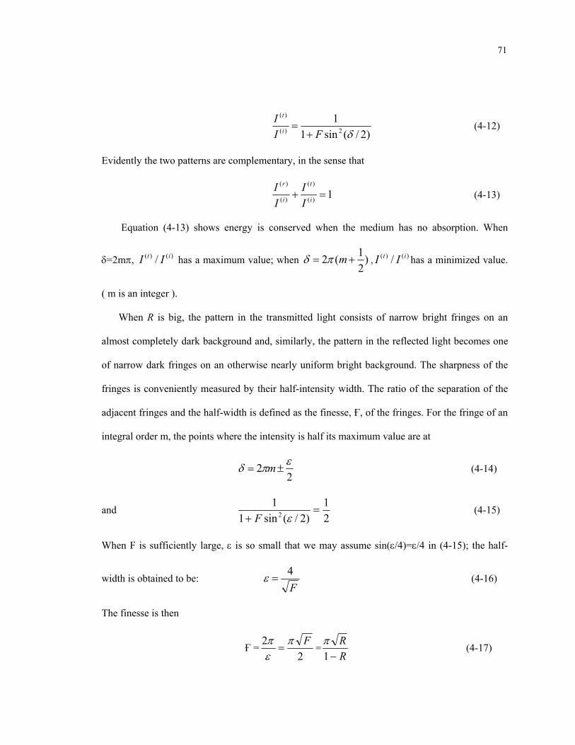
71
)2/(sin11
2)(
)(
δFII
i
t
+= (4-12)
Evidently the two patterns are complementary, in the sense that
1)(
)(
)(
)(
=+ i
t
i
r
II
II
(4-13)
Equation (4-13) shows energy is conserved when the medium has no absorption. When
δ=2mπ, has a maximum value; when )()( / it II )21(2 += mπδ , has a minimized value.
( m is an integer ).
)()( / it II
When R is big, the pattern in the transmitted light consists of narrow bright fringes on an
almost completely dark background and, similarly, the pattern in the reflected light becomes one
of narrow dark fringes on an otherwise nearly uniform bright background. The sharpness of the
fringes is conveniently measured by their half-intensity width. The ratio of the separation of the
adjacent fringes and the half-width is defined as the finesse, Ғ, of the fringes. For the fringe of an
integral order m, the points where the intensity is half its maximum value are at
22 επδ ±= m (4-14)
and 21
)2/(sin11
2 =+ εF
(4-15)
When F is sufficiently large, ε is so small that we may assume sin(ε/4)=ε/4 in (4-15); the half-
width is obtained to be: F4
=ε (4-16)
The finesse is then
Ғ =2
2 Fπεπ
= =RR
−1π
(4-17)
72
Fig. 4.2 shows the behavior of as a function of the phase difference δ for various values
of finesse Ғ.
)()( / it II
Transmission Performance of different Finesse Number
0
0.2
0.4
0.6
0.8
1
5.8 6.3 6.8 7.3 7.8 8.3 8.8
Phase Shift
Tran
smis
sion Finesse=3
Finesse=5Finesse=10Finesse=20
Fig. 4.2 Behavior of as a function of the phase difference δ for various values of finesse
Ғ. Unit of the phase difference δ is π.
)()( / it II
The so far discussed multiple beam interference fringes from a plane parallel plate can also be
applied to the air-gap Fabry-Perot interferometer when the incident light is at near normal
incidence. An air-gap Fabry-Perot interferometer consists of two glass or quartz plates P1, P2
(Fig. 4.3) with plane surfaces. The inner surfaces are coated with partially transparent films of
high reflectivity, and are parallel, so that they enclose a plane parallel plate of air with fixed
separation, d, decided by a spacer. This form of the interferometer is often refered to as Fabry-
Perot etalon.

73
P1 P2
d
Fig. 4.3. Fabry-Perot interferometer
When the incident light is not collimated, the intensity of light I(θ,λ) transmitted through an
ideal Fabry-Perot etalon (one with no defects) is given by
2 2
1( , ) ( )1 (2 / ) sin ( / 2)
I IF
θ λ λπ δ
=+o with
4 cos(nd )π θδλ
= (4-18)
where λ is the light’s wavelength, Io(λ) is the intensity in the center of each fringe, d is the plate
separation, n is the index of refraction of the material between the etalon plates. (for an air-gap,
n=1.0) and F is the finesse of the etalon defined in (4-17). From now on, we will use F to
represent the finesse instead of Ғ. When the light source is monochromatic, the Fabry-Perot
allows transmittance of light at only specific incidence angles. Imaging the output of the Fabry-
Perot produces a series of circular fringes such as those shown in Fig. 4.4. As the wavelength of
the light decreases, the diameters of the rings increase until they eventually occupy the space left
vacant by the next adjacent external ring. As this happens, a new ring appears in the center of the
pattern to replace the old one.

74
Fig. 4.4. Image of the Fabry-Perot interference pattern with monochromatic incident light.
Ideally the finesse F is only a function of reflectivity R, the reflective finesse, if the etalon
plates are perfect with no surface defects and the two etalon-plates are perfectly parallel. Fig. 4.5
shows the relation between the reflective finesse with the reflectivity. In reality, even the best
etalon will possess defects that limit the theoretically expected performance. The actual finesse
will usually be lower than the reflective finesse. If the gap is specified as ,50/λ±d we can
assume the gap will be within these limits for most of its area, say 95%. At any point the most
probable value of the gap thickness is d and the number of places where it departs from this by a
large amount will be very small. The total area where the gap departs from d by an amount
between x and x+dx can be conveniently expressed as the Gaussian formula:
dxxbbAxdA )exp()( 22−=π
, where b is a “figure of merit” which increases as the gap becomes
more and more uniform. Thus different parts of the gap will contribute to the total intensity at
slightly different orders of interference and the effect reveals itself as a convolution of the
theoretical Airy profile with a Gaussian curve. If we assume that near a maximum the Airy
profile is approximately the same shape as a Gaussian curve, and remember that the convolution
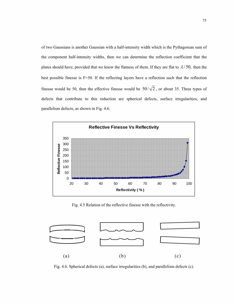
75
of two Gaussians is another Gaussian with a half-intensity width which is the Pythagorean sum of
the component half-intensity widths, then we can determine the reflection coefficient that the
plates should have, provided that we know the flatness of them. If they are flat to ,50/λ then the
best possible finesse is F=50. If the reflecting layers have a reflection such that the reflection
finesse would be 50, then the effective finesse would be 2/50 , or about 35. Three types of
defects that contribute to this reduction are spherical defects, surface irregularities, and
parallelism defects, as shown in Fig. 4.6.
Reflective Finesse Vs Reflectivity
050
100150200250300350
20 30 40 50 60 70 80 90 100
Reflectivity ( % )
Refle
ctiv
e Fi
ness
e
Fig. 4.5 Relation of the reflective finesse with the reflectivity.
(a) (b) (c)
Fig. 4.6. Spherical defects (a), surface irregularities (b), and parallelism defects (c).

76
Effective Finesse VS Defect Finesse
0102030405060708090
20 30 40 50 60 70 80 90 100
Defect Finesse
Effe
ctiv
e Fi
ness
e
FR=50FR=100FR=150
Fig. 4.7. Effective finesse changes with the defect finesse. FR represents the reflective finesse.
The related defect finesse are , , and . The total defect finesse is decided by: dsF dgF dpF dF
22221111
dpdgdsd FFFF++=
The actual effective finesse is decided by: eF
222
111
Rde FFF+=
Fig. 4.7 Plots how the effective finesse changes with the defect finesse for different reflective
finesse.
To use the Fabry-Perot etalon as a filter, it is customary to restrict the incidence angle of the
light to match that of the innermost ring, or spectral element. The resulting field-of-view (FOV) is
given by
8FOV δλλ
= (4-19)

77
where δλ is the spectral resolution of the etalon. The Free Spectral Range (FSR) is defined as the
wavelength difference of the two neighboring constructive interference peaks, or transmission
peaks, and is characterized predominantly by the gap of the etalon. The condition for the
constructive interference is determined by:
2nd mλ
= (4-20)
Where n is the refraction index, d is the gap, λ is the wavelength and m is the order number. Thus
the FSR between the m-th order and the m+1-th order is given by:
2( 1
ndFSRm m
=)+
(4-21)
Normally m is a large number, so it becomes:
2
2FSR
ndλλ= Δ = (4-22)
For the high-resolution etalon, the free spectral range is limited by the aforementioned
effective finesse. In order to expand the free spectral range, two etalons can be used in series, the
one with a larger gap, known as the resolving etalon, defines the spectral resolution of the system.
The etalon with the smallest gap, known as the suppression etalon, suppresses some of the orders
of the resolving etalon. The result is a system with the spectral resolution of the resolving etalon
and a FSR larger or equal to that of the suppression etalon. The latter depends on the ratio of the
FSR of the two etalons with respect to each other.
Suppose that the ratio of the FSR of the suppression etalon to the resolving etalon can be
expressed as ratio of integers A/B, where A and B do not have a common divisor. The FSR of the
twin-etalon system is then given by

78
supFSRBFSRAFSR resol ×=×= (4-23)
Fig. 4.8. Modeling of twin etalon system with the gaps of 3 micron and 12 micron.
Where FSRresol and FSRsup are the free spectral ranges of the resolving and suppression
etalons, respectively. If B = 1, the suppression etalon defines the FSR of the system, otherwise
the FSR of the system will be larger than that of the suppression etalon by a factor of B. In the
twin-etalon system, the FSR of the resolving etalon has now been expanded by the factor A, and
so has the number of available spectral resolution element. The factor A will henceforth be called

79
the FSR expansion factor. Fig. 4.8 models twin etalon system, one with the gap of 3 micron and
the other with a gap of 12 micron.
4.3 Introduction to Liquid Crystal Fabry-Perot (LCFP) Tunable Filter
Tunable filters with a wide tunable range that cover the whole C-band, or L-band, or both,
have found wide applications in fiber optical communication systems, mainly in three domains:
tunable lasers, wavelength division multiplexing systems (WDM), and channel monitoring. Due
to the growing demand in bit-rates and the number of channels in a WDM system, tunable narrow
band pass filters are required [39] .
So far, many efforts have been made to make tunable filters based on the Fabry-Perot
principle [40,41,42]. The tunable optical filters using a torsional actuator [40] need a
high driving voltages up to 500 volts and have a narrow tunable range. The tunable filter [42]
reported by M. Iodice is a temperature-tuned silicon etalon filter with a narrow passband;
however it possesses a narrow free spectral range and the tuning speed was not reported.
3LiNbO
Employing a liquid crystal material as a cavity medium in a Fabry-Perot etalon has many
merits such as low driving voltage, low insertion loss, and wide tuning range. Tunable LCFPs
were first proposed by Maeda in 1990 [43] and Patel in 1992 [44], both from Bellcore.
Hirabayashi et. al. from NTT [45] and Bao et. al. from Colorado University [46] have also
worked on LCFP.
The fabrication of a LCFP device is almost identical to the fabrication of a homogeneously
aligned nematic liquid crystal cell, or an ECB cell. The etalon plates are coated with a conductive
ITO layers, and then high reflection multi-layer dielectric coatings. A polyimide layer with a
thickness of about 50~100 nm is spin-coated on one side and is then uniformly rubbed to generate
the alignment layer for the liquid crystals. The etalon plates are then assembled with spacers to

80
control the thickness of Fabry-Perot cavity. Finally, the liquid crystal material is vacuum-filled
into the cavity. Fig. 4.9 shows the structure of a liquid crystal Fabry-Perot etalon.
ITO layer
High Reflection dielectric coating Liquid
crystal
Etalon Plate
Fig. 4.9 Structure of liquid crystal Fabry-Perot.
The LCFP is polarization dependent. The refractive index for light with a polarization
direction parallel to the rubbing direction, or e-component, is and the refractive index for light
with a polarization direction perpendicular to the rubbing direction, or o-component, is .
LCFPs are tunable only for e-components because can be tuned with an applied voltage, thus
a polarizer is necessary to be placed parallel to the alignment direction of the liquid crystal to
allow the extraordinary mode of light to pass through and block the ordinary mode. When voltage
is applied, the refractive index of the e-component changes along the normal direction of the cell
with a change of the director configuration inside the nematic cell, as was discussed in Chapter 1;
the average refractive index of the e-component inside the cavity is:
,en
on
en

81
∫=d
ee dzznd
n0
)(1 (4-24)
Fig. 4.10 shows how the average refractive index changes with an applied voltage. The model
is based on the modeling of director configuration described in chapter 1. The parameters used for
the model are: =1.79 , =1.53, en on ,0.28,5.15 3311 == KK 5.15// =ε , .2.5=⊥ε The pretilt
angle was assumed to be 0°.
Average Refraction Index Vs Voltage
1.5
1.55
1.6
1.65
1.7
1.75
1.8
1.85
0 2 4 6 8 10
Applied Voltage (v)
Ave
rage
Ref
ract
ion
Inde
x
Fig. 4.10. The average refractive index changes with the applied voltages.
For certain applications, it is desirable to have a tunable filter without a polarization
dependence, such as in fiber optic telecommunication where the polarization state of the optical
signal may be unknown. Several methods have been discussed to fabricate a polarization-
insensitive Fabry-Perot device [50]. Fig. 4.11 shows a solution to achieve the polarization

82
independent optical filtering and tuning. The incident light (polarization state unknown) is
separated into two linearly polarized beams by a polarization beam-splitter. Each beam passes
through a LCFP with the liquid crystal alignment direction parallel to the polarization direction,
and is wavelength-filtered by the tunable LCFP filer. Finally, a second polarization beam splitter
(not shown in the figure) will combine the two filtered beams back into one beam.
•• •
•••
••
••••
••
•
• •
Polarization B eam sp litter
M irro r
L C FP
L C FP
Fig. 4.11. Combination of polarization beam splitter and two LCFPs with alignment directions
perpendicular to each other, to achieve the polarization-independent wavelength filtering.
Fig. 4.12 shows an another solution for a polarization independent optical filtering and tuning
system. Inside the Fabry-Perot cavity, there are two thickness identical liquid crystal layers with
the alignment directions perpendicular to each other. Because of the symmetry, light with any
polarization state has an identical optical path length of tndndn goe ++ , where is the
refractive index of the glass substrate inside the cavity. While in this structure, wavelength
filtering is tunable by changing through an applied voltage; the tunable range is decreased by
gn
en

83
a factor of tndndn
dn
goe
e
++, compared with LCFP with a single liquid crystal layer. The structure
described in Fig. 4.12 is much more compact than that in Fig. 4.11; however, as the glass
thickness t is much larger than the liquid crystal thickness d, the tunable range is very small.
The twisted nematic Fabry-Perot interferrometer (TN-FPI) was proposed by Patel and Lee in
1991 [47]. Here the liquid crystal alignment directions at the two opposite etalon plates are
perpendicular to each other; thus, the liquid crystal layer has a 90° twist through the whole cavity,
as shown in Fig. 4.13. A TN-FPI works in a high driving voltage region, where, in the middle of
the cavity, the liquid crystals are homeotropicly aligned due to the electric field, the two residual
homogeneous liquid crystal layers close to the substrate surfaces will compensate each other and
makes the wavelength-filtering tunable and polarization independent.
••••
••
•••
•••
••
d d
t
Fig. 4.12. Two LC layers inside a Fabry-Perot cavity are used to achieve a polarization
independent wavelength filtering and tuning.
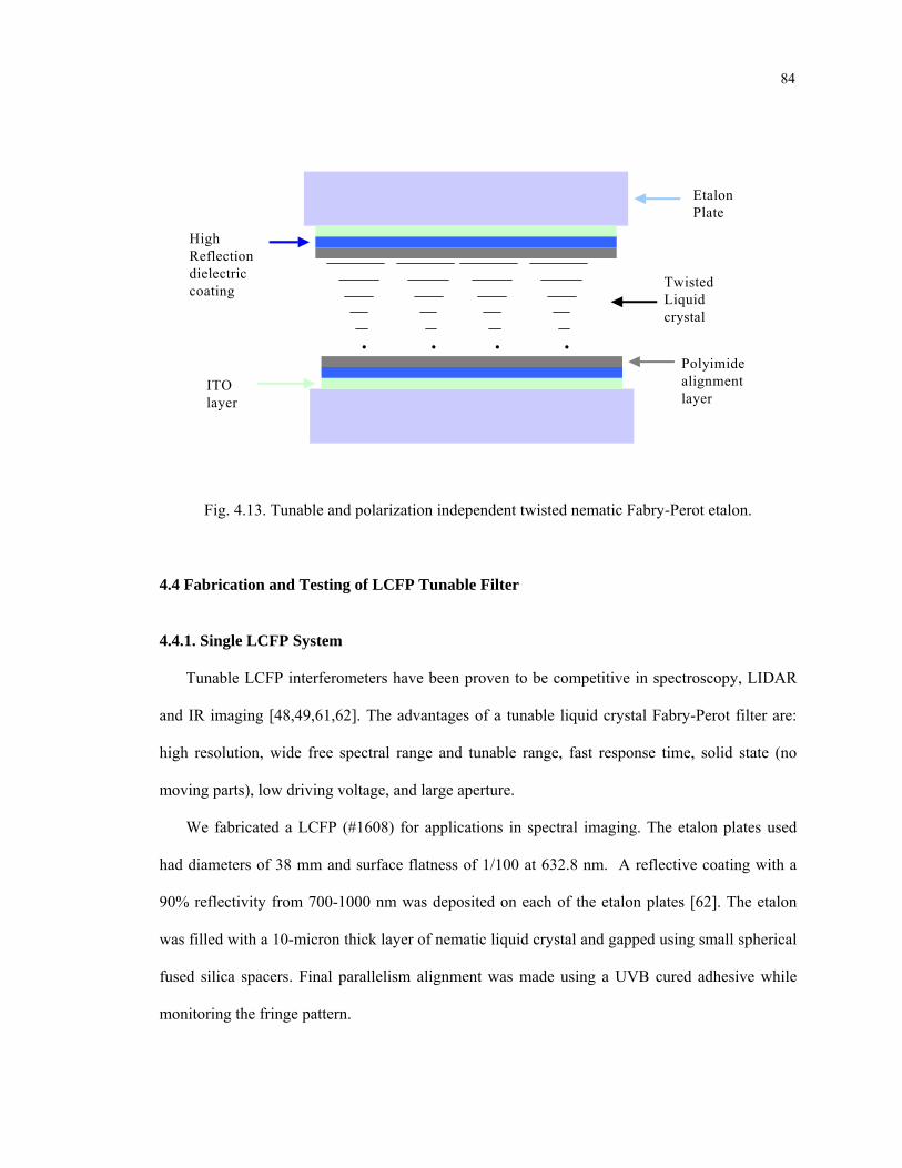
84
ITO layer
High Reflection dielectric coating
Polyimide alignment layer
Twisted Liquid crystal
Etalon Plate
• • • •
Fig. 4.13. Tunable and polarization independent twisted nematic Fabry-Perot etalon.
4.4 Fabrication and Testing of LCFP Tunable Filter
4.4.1. Single LCFP System
Tunable LCFP interferometers have been proven to be competitive in spectroscopy, LIDAR
and IR imaging [48,49,61,62]. The advantages of a tunable liquid crystal Fabry-Perot filter are:
high resolution, wide free spectral range and tunable range, fast response time, solid state (no
moving parts), low driving voltage, and large aperture.
We fabricated a LCFP (#1608) for applications in spectral imaging. The etalon plates used
had diameters of 38 mm and surface flatness of 1/100 at 632.8 nm. A reflective coating with a
90% reflectivity from 700-1000 nm was deposited on each of the etalon plates [62]. The etalon
was filled with a 10-micron thick layer of nematic liquid crystal and gapped using small spherical
fused silica spacers. Final parallelism alignment was made using a UVB cured adhesive while
monitoring the fringe pattern.

85
Transmission curves as a function of wavelength were obtained as shown in Fig. 4.14 through
Fig. 4.16. To make these measurements, light from a monochromator is collimated and passed
through a polarizer before reaching the LCFP that is being tested. The beam is then focussed onto
a photodiode detector and monitored by a computer. The spectral resolution of this set-up is about
0.2 nm, and the beam is collimated such that only the innermost order of the LCFP is sampled.
The polarizer’s aim is to remove the polarization component of the beam that the LCFP cannot
tune. To obtain a transmission curve, the monochromator is scanned in wavelength while a
specific voltage is applied across the LCFP’s gap.
The monochromator is then scanned in wavelength once again with the LCFP out of the
beam. Dividing the former by the latter, the transmission of the LCFP as a function of wavelength
is obtained. The LCFP (#1608) achieved a finesse of 9-12 depending on wavelength and applied
voltage. Peak transmission of polarized light ranged from 40-70%.
The testing was performed on a full working aperture, which is 1.2 inch in diameter, 80% of
1.5 inch. The finesse and free spectral range (FSR) is summarized in Table 4.1. The electro-
optical response measured at the wavelength 805 nm is shown in Fig. 4.17. Fig. 4.18 shows an
image of LCFP #1608 installed in the housing with an electrical connector.
From Table 4.1, the trend is apparent that the finesse increases with the wavelength. This is
because, while the surface quality of the etalon plate is not wavelength dependent in the unit of
nm, it is normally judged by λ/m, where λ is the working wavelength and m is a number, the
defect finesse can be estimated by: = m. This means, suppose the defect finesse at the 500 nm
is 10, the defect finesse at the 1000 nm is ~ 20. Thus the total finesse increases with wavelength
supposing the reflectivity (or reflective finesse) is kept unchanged.
dF

86
We have also successfully fabricated a liquid crystal Fabry-Perot for optical
telecommunication applications. Table 4.2 shows the result of a tunable LCFP filter in the NIR
range (C-band) designed for a tunable laser application. We have successfully modified the high-
reflection coating design to cover the working range from 1520 nm to 1570 nm. We have also
optimized the liquid crystal material and alignment polyimide to minimize the transmission loss.
The cavity gap is controlled by 10 μm spacers.
Finesse and Free Spectral Range of LCFP #1608
Voltage Applied: --> 1.5 V 3.5 V 9 VFinesse at ~ 700 nm 9.7 10.7 9.3
FSR at ~700nm 16.84 nm 18.46nm 19.14nmFinesse at ~ 820 nm 10.7 10.7 9.45
FSR at ~820nm 18.75nm 20.14nm 20.66nmFinesse at ~ 1000 nm 12.4 11.8 10.7
FSR at ~1000nm 26.23nm 27.48nm 28.39nm
Table 4.1. Finesse and free spectral range of LCFP # 1608 at different voltages.
Parameter Measured Value Plate Diameter 10mm
Center Wavelength 1550nm Test Area 0.2 square-mm
Insertion Loss 1.5db Free Spectral Range 4 THz (37nm) Spectral Resolution 108 GHz (1.2 nm)
Finesse 31 Response time 20 ms
Table 4.2. Testing result of tunable LCFP for tunable laser in NIR range.
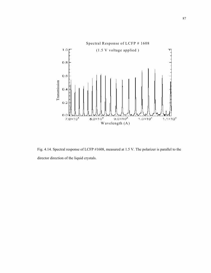
87
W avelength (A )
Tran
smis
sion
Spectral Response of LCFP # 1608
(1.5 V voltage applied )
Fig. 4.14. Spectral response of LCFP #1608, measured at 1.5 V. The polarizer is parallel to the
director direction of the liquid crystals.

88
Spectral Response of LCFP # 1608
(3.5 V voltage applied )Tr
ansm
issi
on
Wavelength (A)
Fig. 4.15. Spectral response of LCFP #1608, measured at 3.5 V. The polarizer is parallel to the
director direction of the liquid crystals.

89
Spectral R esponse of L C FP # 1608
(9 V voltage applied )Tr
ansm
issi
on
W avelength (A )
Fig. 4.16. Spectral response of LCFP #1608, measured at 9.0 V. The polarizer is parallel to the
director direction of the liquid crystals.

90
Voltage Scan of LCFP #1608 ( at 805nm )
Fig. 4.17. Electro-optical response of LCFP #1608, measured at 805 nm.
Fig. 4.18. LCFP #1608 in the housing with electrical connector.

91
4.4.2 Twin LCFP System
We fabricated a twin-LCFP system for the application of high-resolution spectral imaging.
Two LCFP etalons were constructed. Etalon plates have a diameter of 38 mm and a surface
flatness of 1/100 at a wavelength of 632.8 nm. A reflective coating with a 90% reflectivity from
700-1000 nm was deposited on each of the etalon plates. The first etalon (resolving etalon) was
filled with a 30-micron thick layer of nematic liquid crystal and gapped using small spherical
fused silica spacers. Final parallelism alignment was made using a UV cured adhesive while
monitoring the fringe pattern.
Fig. 4.19. Photographs of the single etalon in the housing (right)
and the twin etalon imaging filter (left).
As the high reflection coating exhibit a phase shift upon reflection that altered the effective
gap, the suppression etalon was constructed with a 6 micron gap rather then a 7.5 micron gap in
order to compensate for the phase shift.
The etalons are housed in a cylindrical housing (Fig. 4.19) that consists of an inner cylinder
that holds the etalon with ruby spacers isolating the etalon from the housing. The second cylinder
holds the heating element and thermostat. Using a PID controlled heating system the etalon

92
temperature can be maintained to 0.01 degrees Celsius. The housing has a dovetail flange that
allows the etalons to be connected and then rotated with respect to each other around the optical
axis. This rotational feature allows for the alignment of the polarization states of the etalons to be
co-incident.
Wavelength (Angstrom)
Tran
smis
sion
Fig. 4.20. Transmission as a function of wavelength for the 30 μm gap LCFP.

93
W avelength (Angstrom)
Tran
smis
sion
Fig. 4.21. Transmission as a function of wavelength for the 6 μm gap LCFP.
Fig. 4.20 shows the transmission versus wavelength with an applied potential of 9 Volts, for
the LCFP with 30 μm spacer. Fig. 4.21 shows the same testing for the LCFP with 6.μm spacers.
Both etalons achieved a finesse of 9-12 depending on wavelength and applied voltage. The peak
transmission of polarized light ranged from 40-70% .
4.4.3. Environment Test of LCFP
Two environmental tests were performed at the Utah State University Space Dynamics
Laboratory on etalons similar to those described above. The etalons used in this series of testing
were of a smaller diameter (25 mm) and had a multilayer dielectric reflector with a 90%
reflectivity from 500-700 nm. A gap of 10 microns was used in each etalon. The etalons were

94
tested using the monochrometer described previously and after the shake and thermal-vacuum
tests.
The intent of this test was to thermally cycle the LCFP between at least 40°C and –10°C with
an approximate dwell time of 60 minutes for each of the two temperature extremes and to expose
the etalons to a 10 G shake equivalent to a launch on a Pegasus launch vehicle. The temperature
data from the F-P Liquid Crystal thermal vacuum test is shown in Fig. 4.22.
Initially the temperature cycles did not achieve the required temperature of –10 °C during the
cold cycles. The temperature program was modified to meet the –10 °C requirement, resulting in
five acceptable thermal cycles. The temperature cycling rate was 5 °C/min, with a dwell time of
130 minutes at each end. The thermal couple used to monitor the etalon temperature was
attached to the side of the housing that covered the LCFP.
A cursory examination of the two LCFP etalons did not reveal any obvious damage from
either the shake test or the thermal cycling; the etalon plates were neither chipped nor cracked,
and the electrical wires were still solidly attached to the substrate. Transmission curves as a
function of wavelength were obtained for each of the two etalons using the technique described
previously. This was done for two voltage settings of the LC-FP etalons. As shown in Figures
4.23 and 4.24, the data sets had to be shifted in wavelength for the peaks to be lined up, which
can be attributed to two things. First, uncertainties in the orientation of the LCFP with respect to
the beam can cause a shift of the peak location each time an etalon is set-up in the beam.
Secondly, uncertainties in the absolute wavelength calibration curves could be a factor.
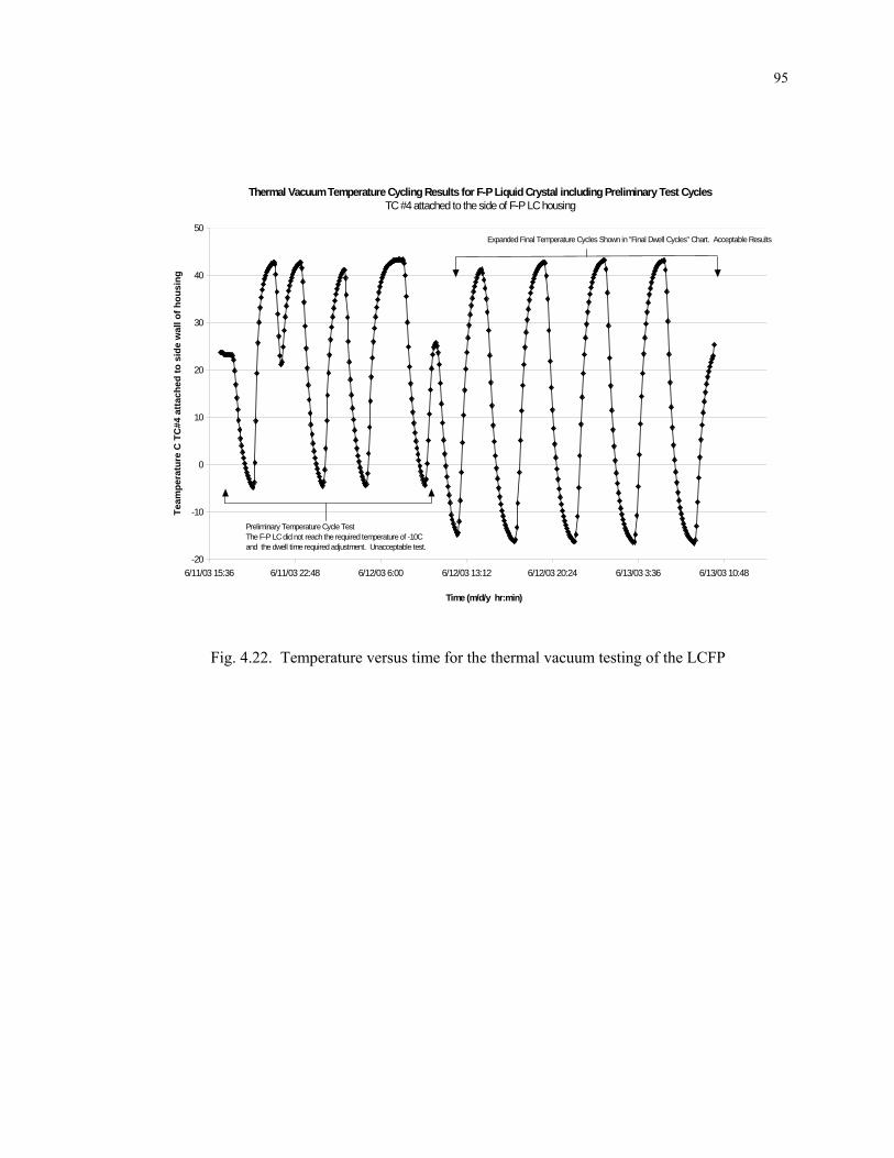
95
Thermal Vacuum Temperature Cycling Results for F-P Liquid Crystal including Preliminary Test CyclesTC #4 attached to the side of F-P LC housing
-20
-10
0
10
20
30
40
50
6/11/03 15:36 6/11/03 22:48 6/12/03 6:00 6/12/03 13:12 6/12/03 20:24 6/13/03 3:36 6/13/03 10:48
Time (m/d/y hr:min)
Team
pera
ture
C T
C#4
atta
ched
to s
ide
wal
l of h
ousi
ng
Preliminary Temperature Cycle TestThe F-P LC did not reach the required temperature of -10Cand the dwell time required adjustment. Unacceptable test.
Expanded Final Temperature Cycles Shown in "Final Dwell Cycles" Chart. Acceptable Results
Fig. 4.22. Temperature versus time for the thermal vacuum testing of the LCFP

96
Fig. 4.23. Transmission of the LCFP that underwent a Pegasus-level shake test for two different
voltage settings (1 and 9 Volt). The offset of the curves in transmission and wavelength is
indicated in parenthesis.

97
Fig. 4.24. Transmission of the LCFP that underwent thermal cycling, before and after the thermal
cycling for two different voltage settings (1 and 9 Volt). The offset of the curves in transmission
and wavelength is indicated in parenthesis.

98
4.5 Summary and Conclusions
We have analyzed, fabricated and characterized liquid crystal Fabry-Perot products for
application in both spectral imaging and optical telecommunication. Both single-etalon and twin-
etalon systems were fabricated. A Finesse of more than 10 in the visible wavelength range and a
finesse of more than 30 in NIR were achieved for the tunable LCFP product.

CHAPTER 5
Switchable Circle-to-Point Converter
5.1 Introduction
This chapter discusses innovative switchable circular-to-point converter (SCPC) devices
based on holographic polymer dispersed liquid crystal (HPDLC) technology, Fabry-Perot
interferometers, and the holographic circular-to-point converter (HCPC). We will discuss the
concept and design of an innovative SCPC device, and the fabrication and characterization of
SCPC devices working at different wavelengths (visible and NIR), and with different channel
numbers (single channel, 10 channel, and 32 channel).
5.2 Background: Introduction to HCPC
Fabry-Perot interferometers (FPI) are employed as spectral-resolving elements in various
applications, such as in Lidar detection of atomospherical, environmental, and climate changes
[48,49] and in telecommunications [43,59]. In a direct detection Doppler Lidar or incoherent
Lidar system to measure wind velocities by aerosol and/or molecular backscatter, the Doppler
shift resulting in a pulse of narrowband laser light from scattering by aerosols or molecules is
measured. A reference spectrum of an outgoing laser beam is measured by the collection of light
scattered from the zero-wind background. When the return signal of a backscattered laser light
passes through the receiving optics, the Doppler shift can be determined by subtracting the
reference spectrum from the return signal. A high resolution Fabry-Perot interferometer is used to
detect the wavelength shifts.
99

100
The Fabry-Perot interferometer produces a circular interference spectrum or fringe patterns of
equal area rings representing equal wavelength intervals, sharing a common axis, at the infinity
focus of an objective lens system. There is a long-established problem of collecting and testing
the signal from the circular fringe pattern as it’s difficult or expensive to design detectors with
ring-shaped geometries.
Different types of image plane detectors have been created which attempt to match the
circular pattern. One such image plane detector was reported by Timothy et al. in 1983 [51].
Their device consisted of an S-20 photocathode, three micro-channel plate electron multiplication
stages, and an equal-area concentric-ring segmented anode to match the interference ring pattern.
Another image plane detector invented by Bissonnette et al. was a multi-element detector of
concentric rings of PIN photodiode material [52, 53]. All of these image plane detectors typically
suffered from blurring of spot sizes and low quantum efficiency.
A different approach for converting the Fabry-Perot fringe pattern itself to fit linear detectors
has also been accomplished [54, 55]. A 45° half angle internally reflecting cone segment is used
to convert the circular Fabry-Perot interferometer fringe pattern into a linear pattern.
McGill and co-workers developed the passive holographic optical element for Lidar detection
[56,57,58]. The holographic optical element comprises areas, each of which acts as a separate
lens to image the light incident in its area to an image point. Each area contains the recorded
hologram of a point source object. The image points can be made to lie in a line in the same focal
plane so as to align with a linear array detector. Holographic Circular-to-point converter (HCPC)
have been developed [57] that have concentric equal areas to match the circular fringe pattern of a
Fabry-Perot interferometer. A HCPC has a high transmission efficiency, and when coupled with a
high quantum efficiency solid state detector, provides an efficient photon-collecting detection
system for a Fabry-Perot interferrometer. The HCPC, as well as other holographic elements, may

101
be used as part of the detection system in a direct detection Doppler Lidar system or multiple
field of view Lidar system.
HCPC holographic plate is divided into concentric annuli. Each annulus of the holographic
plate functions as a single lens and converges the incident beam to a point focus, as depicted in
Fig. 5.1. In order to match the Fabry-Perot fringe pattern, the annuli are designed to intercept
equal wavelength intervals. The signals from different wavelengths are spatially discriminated by
the HCPC device, whereas multiple detectors are required for McGill's HCPC devices.
Fig. 5.1. The ray trace diagram of the holographic circular-to-point converter (HCPC) developed
by McGill and co-workers. All light incident onto a given annulus of the HCPC is redirected to a
designated point. The focal points appear in a common focal plane parallel to the HCPC plate and
are angularly separated.

102
5.3 Principle of Operation of SCPC
The switchable circle-to-point converter (SCPC) is a combination of the HCPC and the
HPDLC that allows for an electric controllability, while maintaining the traditional highlights of a
Fabry-Perot interferometer: high optical throughput and high spectral resolution. Based on
HPDLC technology, the SCPC device is designed to convert the signal from a Fabry-Perot etalon
to a focus point or an array of points just like the HCPC; what is more, the conversion can be
deactivated by applying a strong enough electric field, or the conversion can be electrically
switched on and off [60]. When an Indium Tin Oxide (ITO) conductive layer on one of the SCPC
substrates is patterned with circular pixels that match the Fabry-Perot circular interference
pattern, individual channel are discriminated by the Fabry-Perot etalon and can be separately
selected and switched on and off.
Fig. 5.2 is a cross sectional drawing of a 4x2 switch employing two identical SCPC elements
in series – each element has 4 ring-channels. Both of the SCPC elements have similar ring pixel
patterns geometrically matching the Fabry-Perot interference ring pattern, and both are designed
so that each ring pixel converts the energy within a corresponding circular wavelength channel to
the same point (D1 or D2) when no voltage are applied. To simplify the explanation, only four
ring pixels (or channels) are shown, labeled with 0, 1, 2, and 3. The light source 61 has been
wavelength-discriminated by a FPI. When only voltages V1 and V3 are applied to Channel 1 and
Channel 3 of the first SCPC, respectively, Channel 0 and Channel 2 are routed to the destination
D1, and Channel 1 and Channel 3 are transmitted unimpeded down the optical path. For the
second SCPC, if only ring pixel 1 has an applied voltage, Channel 3 is routed to destination D2,
while Channel 1 passed through along the optical axis. By applying appropriate voltages to
different ring pixels of different SCPC elements, channels can be randomly routed to any
destination.

103
Fig. 5.2.The cross-section drawing of a 4X2 switch employing two identical SCPC elements.
Fig. 5.3 shows a random optical cross-switch can be built by stacking multiple SCPC units.
The collimated light from the Fabry-Perot etalon propagates into the stack of identical SCPC
units. Each SCPC unit converts a selected wavelength channel in the circular interference pattern
to a point, which can be projected onto a detector or routed to different client destinations through
optical fibers.
Fig. 5.3. A random optical cross-switch by stacking multiple SCPC units.

104
5.4 Optics Design of SCPC
Two types of SCPC have been designed. The first type of SCPC is a plain transmission
HPDLC, whose function is steering the beam. The diffracted (steered) beam is focused by a focal
lens to a point, as depicted in Fig. 5.4. In the second type of SCPC, the HPDLC, functioning as a
lens, focuses the collimated incident light to a point, as shown in Fig. (5.2).
C H 1 C H 2 C H 3
S C PC
F ocusingL ens
Fig. 5.4. The first type of SCPC: the diffracted beam is focused by a focal lens to a point.
Left: different channels are routed away by the SCPC and further focused by the focusing lens.
Right: when some channels (red and blue in the figure) on the SCPC are switched on, the
switched channels pass through the SCPC without being steered to the detector.
5.4.1 First Type (Beam Steering) SCPC
In the first type of SCPC device, the HPDLC functions as a beam steering device with the
same diffraction angle dθ everywhere in the HPDLC area (Fig. 5.6). As the SCPC works in the
condition of normal incidence, the HPDLC in the SCPC device requires that the Bragg condition

105
θdi
θt
θd
θr
Diffracted
beam
Glass
Λ
Incident reading beam
θw
Glass
Λ
θw2i
θw1i
θw1
θw2
Recording beams
(a) (b)
Fig. 5.5. Reading beam configuration (a) and recording beam configuration (b) of the beam
steering HPDLC for the first type of SCPC.
be satisfied when the incident beam is normal to the cell surface. The reading beam (wavelength
rλ ) and diffraction beam configuration is illustrated in Fig. 5.5. The HPDLC grating is recorded
by exposing the cell to two interfering laser beams whose wavelength is wλ , as shown in Fig. 5.5
(b). The recording beam incident angles can be determined, provided that the refractive index of
the HPDLC mixture at the recording wavelength wλ , , and the average refractive index of the
HPDLC at the reading wavelength
wn
rλ , is known. rn
The diffraction angle inside the HPDLC diθ is determined by Fresnel's law:
.sinarcsin= ⎟⎟⎠
⎞⎜⎜⎝
⎛
r
ddi n
θθ (5-1)

106
Since the incident beam is perpendicular to the cell surface, the grating plane tilt angle tθ is
the same as the angle between the grating plane and the incident reading beam rθ , therefore,
rtdi θθθ 2=2= . Bragg's law requires that
,=sin2
,=sin2
w
ww
r
rr
n
nλθ
λθ
Λ
Λ
(5-2)
where wθ is the angle between the recording beam and the grating plane. Therefore,
.sinarcsin= ⎟⎟⎠
⎞⎜⎜⎝
⎛
wr
rwrw n
nλλθθ (5-3)
The recording beam incident angles inside the HPDLCs iw1θ and iw2θ , which are defined in
Fig. (5.6b), are then given by
.=,=
2
1
wtiw
wtiw
θθθθθθ
−+
(5-4)
The recording beam incident angles in air are finally determined:
).sin(arcsin=),sin(arcsin=
22
11
iwww
iwww
nn
θθθθ
(5-5)
If we set the diffraction angle of the HPDLC to be , a large angle in order to
minimize the distance between neighboring SCPC devices when they are stacked together, and
assuming that , the recording beam incident angles can be derived:
and .
o79=θ
1.5== rw nn 9543=1 ′owθ
1520=2 ′owθ

107
5.4.2 Second Type (Focusing) SCPC
In the second type of SCPC device, the HPDLC in the SCPC device is designed to focus the
light to a point, functioning like a holographic lens that was demonstrated by Ritcher and co-
workers in 1974 [63].
We constructed an interference pattern using a point source and a plane wave for fabricating
the HPDLC with a built-in focus for the second type SCPC. The holography setup is illustrated in
Fig. 5.6.
532 nm Laser
Mirror
BeamSplitter
HPDLC cell
BeamExpander
Shutter
FocalLens
Iris
Fig. 5.6. The holography setup for fabricating the second type of SCPC.
The point source is generated by adding a focal lens in the optical path of one recording
beam. The focal length of the lens is F , and it is placed at a distance F2 from the sample cell.
The recording and reading optics of the HPDLC across the center of the HPDLC area are
simulated. The recording beam configuration near the sample is illustrated in Fig. 5.7.

108
F
D
A B C
θ 2w A
θ 2w Bθ 2w C
θ 1w A
θ 1w Bθ 1w CF
D
A B C
θ 2w A
θ 2w Bθ 2w C
θ 1w A
θ 1w Bθ 1w C
Fig. 5.7. Recording beam profile across the HPDLC area using the setup shown in Fig. 5.6.
5.4.3 Astigmatism in Second Type (Focusing) SCPC
For the SCPC working at a wavelength (such as 1540 nm) different from the recording
wavelength (such as 532 nm), astigmatism are explained in our following simulation and
calculation, and also confirmed in our testing results.
In our modeling, we still set the diffraction angle at the center of the HPDLC to be
and ; the recording beam incident angles at the center of the HPDLC are:
and , as calculated in the previous section. The diameter of the
effective HPDLC area is cm. For the collimated recording beam, the incident angle is
identical at different locations of the HPDLC: . The incident angles
of the diverging recording beam at different locations are calculated for different
o79=θ 1.5== rw nn
9543=1 ′owθ 1520=2 ′o
wθ
2.54=D
1520=== 222 ′oCwBwAw θθθ
F . The
incident angles at spot A and spot C are presented in Table 5.1, wherethe values are defined by:

109
:rbAθ the Bragg matched incident angle for 1540 nm at A; :rbCθ the Bragg matched incident
angle for 1540 nm at C; :dbAθ the Bragg diffraction angle at point A; :dbCθ the Bragg
diffraction angle at C; :dnAθ the diffraction angle with 1540 nm normal incidence at A; :dnCθ
the diffraction angle with 1540 nm normal incidence at C; TIR: total internal reflection; d:
minimum distance between neighboring electrodes determined by the diffracted beam
configuration.
With the incident angles of the recording beams determined, we calculate the Bragg matched
incident angle and diffraction angles for the 1540 nm reading beam on different locations across
the HPDLC area. Along the line ABC as shown in Fig. 5.7, the normal incident light at point B,
center of the SCPC, is no doubt Bragg-matched; however, as the incident location moves away
from the center B, the normal incidence is no more Bragg matched. At points A and C which
show the largest deviations from normal incidence, the Bragg matched incident angles rbAθ
and rbCθ , and the corresponding diffraction angles dbAθ and dbCθ , are calculated and listed in
Table 5.1. Considering the angular dependence of the diffraction efficiency discussed in Chapter
2, our calculated result indicates:
(1) The diffraction efficiency for normal incident of 1540 nm light decreases with the
increase of the distance from the incident spot to the center of the HPDLC.
(2) The deviation of the Bragg matched incidence from the normal incidence decreases with
increasing F .
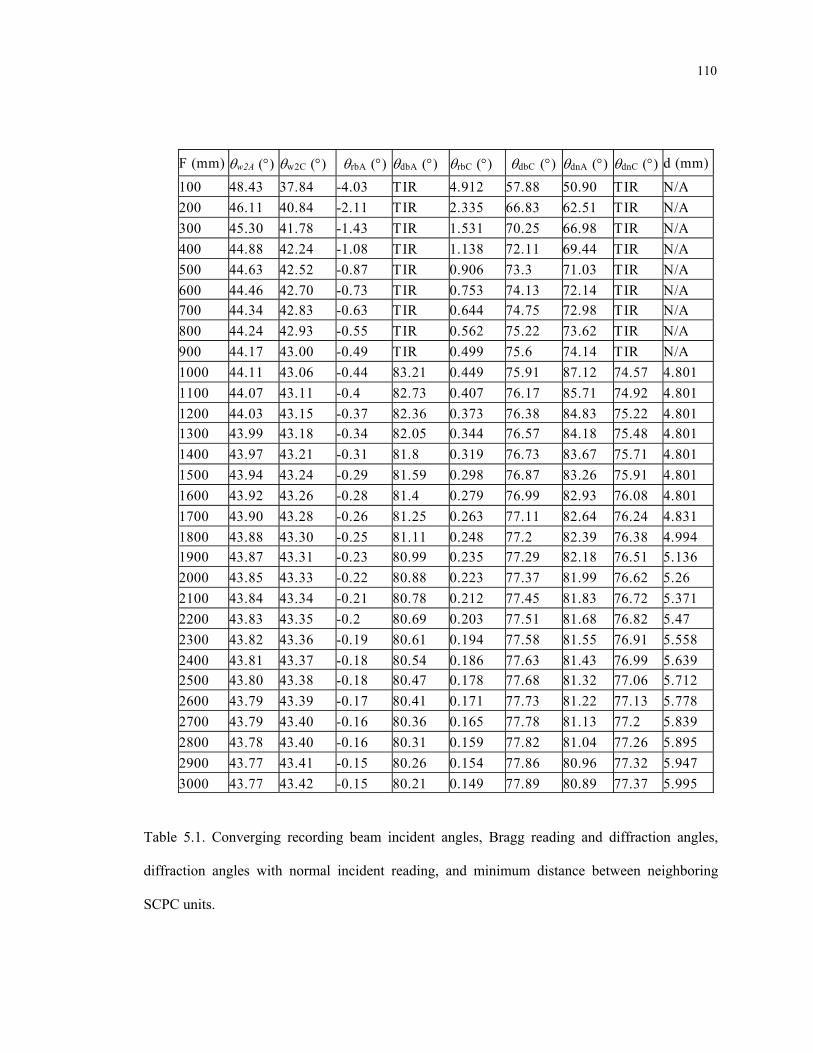
110
F (mm) θw2A (°) θw2C (°) θrbA (°) θdbA (°) θrbC (°) θdbC (°) θdnA (°) θdnC (°) d (mm)
100 48.43 37.84 -4.03 TIR 4.912 57.88 50.90 TIR N/A 200 46.11 40.84 -2.11 TIR 2.335 66.83 62.51 TIR N/A 300 45.30 41.78 -1.43 TIR 1.531 70.25 66.98 TIR N/A 400 44.88 42.24 -1.08 TIR 1.138 72.11 69.44 TIR N/A 500 44.63 42.52 -0.87 TIR 0.906 73.3 71.03 TIR N/A 600 44.46 42.70 -0.73 TIR 0.753 74.13 72.14 TIR N/A 700 44.34 42.83 -0.63 TIR 0.644 74.75 72.98 TIR N/A 800 44.24 42.93 -0.55 TIR 0.562 75.22 73.62 TIR N/A 900 44.17 43.00 -0.49 TIR 0.499 75.6 74.14 TIR N/A 1000 44.11 43.06 -0.44 83.21 0.449 75.91 87.12 74.57 4.801 1100 44.07 43.11 -0.4 82.73 0.407 76.17 85.71 74.92 4.801 1200 44.03 43.15 -0.37 82.36 0.373 76.38 84.83 75.22 4.801 1300 43.99 43.18 -0.34 82.05 0.344 76.57 84.18 75.48 4.801 1400 43.97 43.21 -0.31 81.8 0.319 76.73 83.67 75.71 4.801 1500 43.94 43.24 -0.29 81.59 0.298 76.87 83.26 75.91 4.801 1600 43.92 43.26 -0.28 81.4 0.279 76.99 82.93 76.08 4.801 1700 43.90 43.28 -0.26 81.25 0.263 77.11 82.64 76.24 4.831 1800 43.88 43.30 -0.25 81.11 0.248 77.2 82.39 76.38 4.994 1900 43.87 43.31 -0.23 80.99 0.235 77.29 82.18 76.51 5.136 2000 43.85 43.33 -0.22 80.88 0.223 77.37 81.99 76.62 5.26 2100 43.84 43.34 -0.21 80.78 0.212 77.45 81.83 76.72 5.371 2200 43.83 43.35 -0.2 80.69 0.203 77.51 81.68 76.82 5.47 2300 43.82 43.36 -0.19 80.61 0.194 77.58 81.55 76.91 5.558 2400 43.81 43.37 -0.18 80.54 0.186 77.63 81.43 76.99 5.639 2500 43.80 43.38 -0.18 80.47 0.178 77.68 81.32 77.06 5.712 2600 43.79 43.39 -0.17 80.41 0.171 77.73 81.22 77.13 5.778 2700 43.79 43.40 -0.16 80.36 0.165 77.78 81.13 77.2 5.839 2800 43.78 43.40 -0.16 80.31 0.159 77.82 81.04 77.26 5.895 2900 43.77 43.41 -0.15 80.26 0.154 77.86 80.96 77.32 5.947 3000 43.77 43.42 -0.15 80.21 0.149 77.89 80.89 77.37 5.995
Table 5.1. Converging recording beam incident angles, Bragg reading and diffraction angles,
diffraction angles with normal incident reading, and minimum distance between neighboring
SCPC units.

111
For points A and C, the diffraction angles dnAθ and dnCθ for normal incident reading at 1540
nm are also calculated and listed in Table 5.1. These angles are not Bragg matched. It is important
to notice that when is less than 1000 mm, the diffraction beam at the left edge, A, will be
totally reflected at the glass-air interface and trapped in the HPDLC until finally escaping from
the edge. This total internal reflection (TIR) effect further decreases the diffraction efficiency at
the edge of the HPDLC area. To avoid the TIR effect, the focal length of the lens should be larger
than 1000 mm.
F
When the diffraction angles are known, the converging properties of the diffracted beam in
the yx − plane can be derived from Bragg's law. Fig. 5.8 shows the converging properties of the
diffracted beams across the center of the cell in the direction. The focus is not ideal in the y
yx − plane. With the increase of F , the waist of the diffracted beam (the thinnest width of the
diffracted beam) decreases, and the position of the beam waist moves away from the HPDLC. To
obtain a relatively good focus, a lens with a large focal length is preferred in the recording setup.
Since the lens is placed at F2 from the HPDLC during exposure, a large F brings
inconvenience to the fabrication process. Two focal lenses in series can be used to generate the
same diverging recording beam profile at the position of the HPDLC.
In the simulation above, only the locations across the center of the HPDLC area are
considered. A qualitative simulation of various locations over the entire HPDLC area using
ZEMAX, an optical simulation and design software, reveals that the focusing of the diffracted
beam is also astigmatic, which matches well with our calculation and analysis. The convergence
of the diffracted beam in the yx − plane is faster than that in the z direction. Therefore the linear
dimension of the focus “point” is larger than that of the beam waist calculated in the simulation
above.

112
x
y
F = 1000
A B C
F = 2000
A B C
x
y
F = 3000
A B C
x
y
Fig. 5.8. The diffraction beam profile of 1 inch HPDLCs fabricated using lenses with various
focal length F .

113
5.5 Fabrication and Characterization of SCPC Working in Visible Wavelengths
5.5.1 Single Channel SCPC
For SCPCs working in visible wavelengths, we began sample fabrication with the non-
pixelated HPDLC for the second type of SCPC devices, or single channel SCPC devices with
built-in convergence, using ITO glass substrates. A UV-curing mixture consisting of 50% PN393
and 50% liquid crystal TL 205 was prepared. The HPDLC mixture was sandwiched between two
substrates with the cell gap controlled by 15 μ m fiber spacers. The cell was exposed to a 351 nm
Ar+ ion UV laser for 90 seconds in holographic setup as illustrated in Fig. 5.6. The intensity of a
single recording beam was ~ 600 mW/cm . 2
F o c a l P o in t
Z e ro O rd e r
L e ft: N o v o lta g e a p p lie d ; R ig h t: V o lta g e a p p lie d . (1 0 0 V A C sq u a re -w a v e 1 k H Z )
Fig. 5.9. The left panel : the switch-off state of the SCPC (no voltage applied); the right panel :
the switch-on state (voltage applied). In each panel, the holographic focal point is the point on
the right side, and the “pass-through” light is on the left.

114
Fig. 5.9 shows digital images of a HPDLC sample working with a red laser (632.8 nm),
showing the switching of the focal point of the SCPC. The image on the left panel is the switch-
off state of the SCPC when no voltage is applied, and the image on the right panel is the switch-
on state when a 100 V square-wave AC 1 KHz signal is applied. On each panel, the large light
spot is the pass-through light, or zero order, and the left fine point is the focal diffracted light. The
diffraction angle away from the transmission beam is 45°. The holographic focal point was
sampled with a detector, and the contrast ratio of the switch-off versus switch-on state is 50:1.
The overall efficiency of the hologram was 30%. The loss of the efficiency comes from the
scattering of the materials, and reflection from the surfaces as no AR coating is used on the glass
substrates.
We also developed a formula for green-laser (532 nm) curing. The materials are various
ratios of Ebecryl 8301 and 4866 as pre-polymer bases to control the effective functionality of the
polymer. These are mixed with the nematic liquid crystal BL038 ( =1.527, =1.799) from EM
Industries. Rose Bengal and N-Phenylglycine were selected as the photoinitiator and coinitiator
that are sensitive to the visible light. The solution of photoinitiator was prepared with 4.0 wt.%
Rose Bengal and 10.0 wt.% N-Phenylglycine in N-Vinyl Pyrrolidinone. The surfactant Sorbitan
Mono-Oleate was also added to the mixture, which is known to reduce the surface interaction
strength between the liquid crystal and polymer. The weight ratio of Oligomer: liquid crystal:
initiator solution: surfactant was 45: 32.4: 12.6: 10. A droplet of the pre-polymer mixture was
sandwiched between two AR-coated ITO glass substrates with 5-micron spacing thickness
controlled with glass fiber spacers. The SCPC sample is exposed to a 5W green laser at a
wavelength of 532 nm for 30 seconds.
on en
Fig. 5.10 shows two images of a single channel SCPC device in operation fabricated with
green-laser curing. The beam size of the reading laser (532 nm) is about one-half inch, shown as

115
the large spots in both left panel and right panel. The SCPC converts the incident light into a fine
point (the small spots in both images) that is 45° off axis from the center of the SCPC. The
focusing effect of the SCPC is very good, with a focus length of 10 cm, matching the writing
condition. The right image in Fig. 5.10 shows the SCPC switched by an AC field of 160 Volts, 1k
Hz. A Melles Griot laser power meter was utilized to measure the intensity of the incident beam
(Iin) and the transmitted beam (I0th), and an OPHIR infrared power meter was employed to
measure the diffracted beam intensity (I1st). The transmittance was calculated as I0th/ Iin, and the
diffraction efficiency was calculated as I1st/ Iin. The testing result are detailed in Table 5.2. The
contrast ratio of switch-off to switch-on is larger than 40.
Transmittance I0th/ Iin Diffraction Efficiency I1st/ Iin Switch On 95% 5% Switch Off 5% 80%
Table 5.2 Testing result of SCPC.
Fig. 5.10. Switching of a SCPC working at 532 nm.

116
5.5.2 10-channel SCPC
The SCPC is designed to work in tandem with a Fabry-Perot etalon to convert the circular
interference fringe pattern into points or a point array. Thus the ring pixels of the ITO pattern on
one SCPC substrate must match the Fabry-Perot ring. Fig. 5.11 shows an ITO ring pattern for a
10-channel SCPC.
Fig.5.11. A schematic description of CAD design of a 10-pixel ITO pattern in SCPC
The fabrication of a multiple channel SCPC is similar to the fabrication of one-pixel SCPC,
because the holographic pattern in all the pixels are written at the same time. A 10-pixel SCPC
working for 532 nm was fabricated. Fig. 5.12 shows the switching of the center pixel of the 10-
pixel SCPC that focuses 10 channels to one point. On both the left and right images, the left light
spot (bigger spot) is the light that pass through the SCPC, the right spot (smaller) is the focusing
point. In the left image, the center pixel is switched on with a voltage of 150 Volts. In the right
image, no voltage is applied. Because all of the 10 pixels focus on one point, there is still light on
the focusing point when the center pixel is switched on.
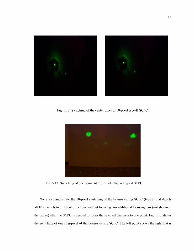
117
Fig. 5.12. Switching of the center pixel of 10-pixel type-II SCPC.
Fig. 5.13. Switching of one non-center pixel of 10-pixel type-I SCPC
We also demonstrate the 10-pixel switching of the beam-steering SCPC (type I) that directs
all 10 channels to different directions without focusing. An additional focusing lens (not shown in
the figure) after the SCPC is needed to focus the selected channels to one point. Fig. 5.13 shows
the switching of one ring-pixel of the beam-steering SCPC. The left point shows the light that is

118
steered by the SCPC, the right point is the light passing through. The left point and the right point
have the same size. When the ring-pixel is switched on with a voltage of 150 volts, all of the
signal from the selected ring-pixel pass through without being steered to the left point, so a black
ring appears in a bright background that is the other 9 channels (including the center pixel). Fig.
5.14 shows the switching of the center pixel of a beam-steering SCPC.
Fig.5.14 Switch on the center pixel of a beam-steering 10-channel SCPC.
5.6 Fabrication and Characterization of SCPC Working in NIR Wavelengths
5.6.1 Material Optimization for Big-Area SCPC Working in NIR
The HPDLC materials can be divided into two categories: UV curable materials and visible
curable materials. Both materials have been used to demonstrate the SCPC concept working in
the visible wavelength range. When fabricating the SCPC with a large area (minimum 2.54 cm
diameter) working in the 1550 nm wavelength range, a 532 nm laser instead of a UV laser is used

119
for the holographic recording, due to the lack of sufficient power in the UV laser, and the high
efficiency of visible curable materials.
Material optimization was initiated from several base formulas with different monomers and
surfactants. The liquid crystal in all these formulas is BL038, a liquid crystal mixture from EMD
Chemicals that has a high optical birefringence (0.27). The contents of the HPDLC mixtures are
listed in Table 5.3. The monomer mixture in Formula 1 consists of the urethane acrylate
monomers Ebecryl 8301 and Ebecryl 4866, both of which are produced by UCB Chemicals.
Sorbitan mono-oleate, S-271 by Chem Services, is utilized as a surfactant to reduce the switching
voltage. The monomer mixture in Formula 2 consists of Ebecryl 8301 and Trimethylolpropane
tris (3-mercaptoporpionate) (TT3) from Sigma-Aldrich. A fluorinated acrylate monomer,
1,1,1,3,3,3 – Hexafluoroisopropyl Acrylate (HFIPA) is utilized as a surfactant in Formula 2. The
monomer in Formula 3 is Dipentaerythritol Pentaacrylate (DPHA), a tetra-functional monomer.
A mono-functional monomer, Vinyl Neononanoate (VN), serves as the surfactant in this formula.
Photoinitiator solutions are required in all of these formulas to enable the photo polymerization
and for resolving the liquid crystal in the monomers. The photo initiator solutions consist of Rose
Bengal (photoinitiator), N-Phenylglycine (NPG, co-initiator) and 1-Vinyl-2-Pyrrolidinone (NVP,
solvent and chain terminator), all available from Sigma- Aldrich.
The HPDLCs fabricated using these materials were characterized and several issues arose.
As the operation wavelength of the HPDLC is ~1500 nm, a 15-micron cell gap is necessary to
achieve sufficient diffraction efficiency. The switching voltage necessary to completely
deactivate the HPDLC is high (> 250V), and the samples may experience a dielectric breakdown
when a high voltage is applied across the cell. The surfactant in Formula 1 introduces ions into
the HPDLC and substantially increases the conductance of the HPDLC. The HPDLCs fabricated
using Formula 1 material are easy to heat up when a voltage is applied and experience thermal

120
switching instead of electrical switching. Significant effort was made to search for an appropriate
HPDLC formula that solved these issues. When the liquid crystal BL011 is used to replace the
liquid crystal BL038 in all three formulas, a reduction in the switching voltage was observed;
however, the diffraction efficiency also decreased substantially. Signs of thermal switching were
also observed in some of the samples. It is clear the BL011 formulas were not suitable for the
device. Materials based on the three original formulas but with varied component ratios were
further investigated.
Formula 1
Ebecryl 8301 Ebecryl 4866 BL038 P.I.Solution 1 S-271
22.50% 22.50% 32.40% 12.60% 10.00% Formula
2 Ebecryl 8301 TT (3) BL038 P.I.Solution 2 HFIPA
36% 4% 34% 16% 10% Formula
3 DPHA BL 038 P.I.Solution 1 VN
47% 38% 10% 5%
Rose Bengal NPG NVP P.I.Solution 1 4% 10% 86% P.I.Solution 2 3% 7% 90%
Table 5.3. Components of the HPDLC mixtures initially investigated.
After a series of experiments, a HPDLC mixture that is suitable for the HPDLC operating at
~ 1500nm based on Formula 3 is developed. The contents of the new formula (Formula-SCPC)
are presented in Table 5.4.

121
Formula-SCPC
DPHA BL038 P.I.Solution 1 VN
35.92% 43.36% 10.45% 10.27%
Table 5.4. Material contents of Formula-SCPC.
5.6.2 Fabrication and Characterization of Single Channel SCPC Working in NIR
As we have discussed in the optical design of the SCPC, the type-II (focusing) SCPC
working at 1550 nm has strong astigmatism, which is also confirmed in testing of our type-II
samples working at 1550 nm. The focusing in the yx − plane was faster than in the z direction,
which is in agreement with the results of our qualitative simulation. Our research focuses on type-
I (beam-steering) for SCPC devices working at 1550 nm.
532 nm Laser
Sample
θw2
Mirror
BeamExpander
Shutter
Iris
Beam Splitter
θw1 532 nm Laser
Sample
θw2
Mirror
BeamExpander
Shutter
Iris
Beam Splitter
θw1
Fig. 5.15. Holographic recording setup for fabricating the SCPCs working in the 1550 nm range.
We fabricated the single channel HPDLC using ITO-coated glass substrates with AR coating.
The “Formula-SCPC” HPDLC mixture was sandwiched between two substrates. The cell gap
was controlled by 15 μ m fiber spacers. The cell was exposed in the holographic setup illustrated
in Fig. 5.15 for 90 seconds. The recording beam incident angles at the HPDLC were:

122
9543=1 ′owθ and to enable a large diffraction angle of . The intensity of a
single recording beam was 600 mW/cm .
1520=2 ′owθ o79=θ
2
We characterized the electro-optical properties of the HPDLCs fabricated for the SCPC
device. All of the HPLDCs showed strong polarization dependence. The diffraction efficiency for
s-polarized light was much less than that of the p-polarized light and was therefore neglected,
only p-polarized light was tested. A 1 KHz square wave signal was used to address the HPDLCs.
The transmittance and diffraction efficiency as a function of voltage are presented in Fig. 5.16.
The switching voltage was substantially decreased and the diffraction efficiency was 55%.
Electro-Optical Response of SCPC
0
0.1
0.2
0.3
0.4
0.5
0.6
0 20 40 60 80 100 120 140 160
Voltage ( v )
Effic
ienc
y
TransmissionDiffraction
Fig. 5.16.Transmittance and diffraction efficiency as a function of voltage.
Compared with the high diffraction efficiency (80%) of the SCPC working at 532 nm, a
number of factors lower the diffraction efficiency of the SCPC operating at 1550 nm:
(1) The Pitch of grating of the HPDLC is much larger;
(2) The AR coating is optimized for 532 nm, not 1550 nm;

123
(3) The Sharp diffraction angle further degrades the AR coating performance;
5.6.3. Fabrication and Characterization of 32-channel SCPC Working in NIR
5.6.3.1 Fabrication Process
The 32-channel SCPC units were fabricated with AR ITO-coated substrates with thickness of
0.5 mm, thinner than the previously used glass substrates with a thickness of 1.0 mm. The
purpose of using the thin glass is to minimize the size of the total device when multiple SCPC
units must be stacked together. To hold the cells of the thin substrates properly during exposure, a
special sample holder was designed and fabricated.
The holographic recording setup for fabricating the SCPC units is illustrated in Fig. 5.15. The
two recording beam incident angles were set to be 1wθ =41°25′, and 2wθ =18°25′, for the normal
incidence reading beam to be diffracted to a large angle of . The Formula-SCPC material
was utilized. 15-micron fiber spacers controlled the cell gap. The cells were pressed at 4.5 psi by
a balloon for 12 minutes to ensure cell gap homogeneity prior to the holographic exposure. The
exposure time was 5 minutes and the total output power of the laser was set to 3W during the
exposure. After exposure, the cell was cured in a 3W laser beam to polymerize the monomers
outside the HPDLC area. The edges of the cells were secured with 5-minute epoxy.
o79=θ
5.6.3.2 Switching of the 32-channel SCPC
The switching properties of the SCPC were investigated. The driving signal was a 1kHz
square wave generated by a HP function generator and a Trek amplifier. Voltage was applied on
each of the 32-channels of the SCPC unit one channel at a time, and the switching of each single
ring pixel was observed. Fig. 5.17 demonstrates the switching of several channels of a SCPC
sample.
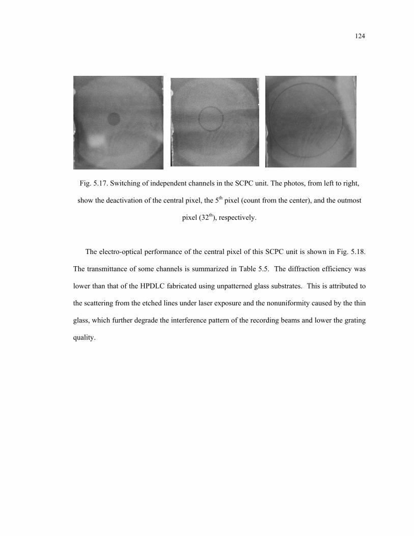
124
Fig. 5.17. Switching of independent channels in the SCPC unit. The photos, from left to right,
show the deactivation of the central pixel, the 5th pixel (count from the center), and the outmost
pixel (32th), respectively.
The electro-optical performance of the central pixel of this SCPC unit is shown in Fig. 5.18.
The transmittance of some channels is summarized in Table 5.5. The diffraction efficiency was
lower than that of the HPDLC fabricated using unpatterned glass substrates. This is attributed to
the scattering from the etched lines under laser exposure and the nonuniformity caused by the thin
glass, which further degrade the interference pattern of the recording beams and lower the grating
quality.

125
Electro-optical Response of SCPC
0102030405060708090
100
0 20 40 60 80 100 120 140 160
Applied Voltage ( v )
unit
(%)
TransmissionDiffraction
Fig. 5.18. The normalized transmittance and diffraction efficiency of the center channel
of a SCPC unit as a function of voltage.
Channel Number Ton (%) Toff (%)1 45.7 62.22 50 69.3 52 66.
13 56.7 73.316 57.5 78.719 58.7 81.624 62.3 76.326 64.6 78.328 67.6 82.7
19
Table 5.5. The transmittance of some channels of a SCPC unit.

126
5.6.3.3 Wavelength Dependence
The SCPC device was designed to operate in the wavelength range of 1530- 1560 nm.
Therefore, the wavelength dependence of the device performance was a critical factor. An
Agilent 81689A tunable laser was utilized to characterize the wavelength dependence of the 32-
channel SCPC devices. The measurement setup is illustrated in Fig. 5.19. The incident light was
perpendicular to the SCPC cell surface. The intensity of the incident light, the transmitted light,
and the diffracted light was measured using a Melles Griot universal power meter at various
wavelengths. The zero field transmittance and diffraction efficiency of the SCPC device were
calculated and the results are presented in Fig. 5.20.
Agilent 81689A Tunable Laser
Collimation Lens
Photo Detector
Iris
Iin I0th
I1st
Agilent 81689A Tunable Laser
Collimation Lens
Photo Detector
Iris
Iin I0th
I1st
Fig. 5.19. Optical setup for measuring the wavelength dependence of the SCPC units.
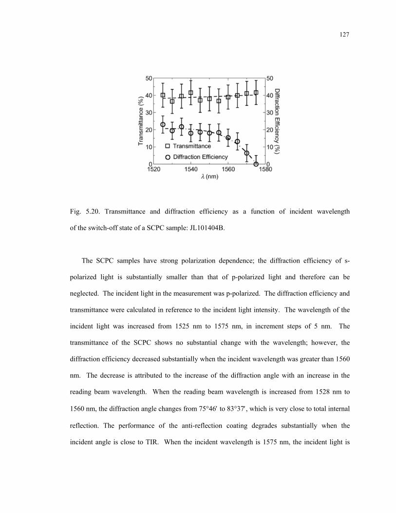
127
Fig. 5.20. Transmittance and diffraction efficiency as a function of incident wavelength
of the switch-off state of a SCPC sample: JL101404B.
The SCPC samples have strong polarization dependence; the diffraction efficiency of s-
polarized light is substantially smaller than that of p-polarized light and therefore can be
neglected. The incident light in the measurement was p-polarized. The diffraction efficiency and
transmittance were calculated in reference to the incident light intensity. The wavelength of the
incident light was increased from 1525 nm to 1575 nm, in increment steps of 5 nm. The
transmittance of the SCPC shows no substantial change with the wavelength; however, the
diffraction efficiency decreased substantially when the incident wavelength was greater than 1560
nm. The decrease is attributed to the increase of the diffraction angle with an increase in the
reading beam wavelength. When the reading beam wavelength is increased from 1528 nm to
1560 nm, the diffraction angle changes from 75°46′ to 83°37′, which is very close to total internal
reflection. The performance of the anti-reflection coating degrades substantially when the
incident angle is close to TIR. When the incident wavelength is 1575 nm, the incident light is

128
totally reflected at the glass-air interface. The diffraction efficiency is fitted with the coupled
wave theory for a transmission grating,
( )( )
.2
1sin
2
=cos0cos
=1/22
22
2
2
12
1
22
2
⎪⎭
⎪⎬⎫
⎪⎩
⎪⎨⎧
⎥⎥⎦
⎤
⎢⎢⎣
⎡⎟⎠⎞
⎜⎝⎛ Δ
+
⎟⎠⎞
⎜⎝⎛ Δ
+κακ
ακ
κθθ
η LA
LA (5-6)
where )cos(/)2cos(1 BBnk θλθπ= , Bn θ
λπαcos
=0Λ
ΔΛ
−Δ is the phase mismatch generated
from the deviation in wavelength. As the recording beam incident angles are: 1wθ =43°59′ and
as shown in Fig. 5.6(b), the writing angle 1520=2 ′owθ wθ inside the HPDLC is determined by:
2 wθ = arc(sin( 1wθ )/1.5) - arcsin(sin( 2wθ )/1.5); wθ = 6.9264°. Considering a writing wavelength
of λ=532 nm and refractive index n ~ 1.5, the period of the grating Λ is λθ =sin2 wnΛ and
calculated to be Λ = 1.478 μm. For a reading beam with normal incidence on the cell surface, as
the designed exit angle in air is 79°, the Bragg angle is 2θB =arcsin((sin(79°))/1.5),
θB = .(see Fig. 5.2(a)). The wavelength that meets the Bragg condition is: o44.20
BB n θλ sin2 Λ= =1.548 μm. As the wavelength varies from Bλ , the diffracted angle shifts to
meet the condition of constructive interference: n/=sinsin λθθ ′Λ+Λ , as the grating can be
treated as a thin grating (defined in Chapter 2). When the diffracted light passes through the
glass-air boundary, the intensity of the refracted light is [64]:
222// )
)(cos)(sin2sin2sin(
didddi
ddiIθθθθ
θθ−+
= (5-7)
Considering the coupled wave theory and the light refraction equation (5-7), we fit the
modeling result with the measurement result, as shown in Fig. 5.21. The model does not consider

129
the effect of scattering, which may explain the discrepancy between the model and the
experimental result.
Wavelength Dependence of Diffraction Efficiency
0
0.05
0.1
0.15
0.2
0.25
1520 1530 1540 1550 1560 1570
Wavelength
Diff
ract
ion
Effic
ienc
y
a
Modeling Measurement
Fig. 5.21. Fit of the model based on coupled wave theory and the refraction principle, with the
experimental result, for the wavelength dependence of the diffraction efficiency.
5.6.3.4 Angular Dependence
The dependence of the transmittance and diffraction efficiency on the reading beam incident
angle was characterized to evaluate the holographic recording optical setup. A 1540 nm fiber
laser generated the incident beam. The transmitted beam intensity and diffracted beam intensity
were measured using a Melles Griot universal power meter and an OPHIR infrared power meter
with various reading beam incident angles. The transmission as a function of incident angle is
presented in Fig. 5.22, and the diffraction efficiency as a function of incident angle of the SCPC
is presented in Fig. 5.23. Both Fig.s 5.22 and 5.23 are based on the test result of SCPC sample

130
JL101404B. The diffraction efficiency reached its maximum at normal incidence, while the
transmittance minimized at an incident angle of 1°. This result proved the choice and control of
recording beam incident angle was optimized for normal incidence reading of the designated
wavelength. When the reading beam incident angle was greater than 1°, the diffraction efficiency
decreased much faster than the increase of the transmittance. The abruptness of the decrease in
diffraction efficiency was due to the increase of the diffraction angle with the increase of the
incident angle. The designed diffraction angle in the device was 79° in air and the diffraction
angle inside the SCPC was close to the total reflection angle at the glass-air interface. The
efficiency of the anti-reflection coating on the glass substrates decreased substantially when the
diffraction angle was close to the total internal reflection angle and the diffracted light would be
totally reflected when the total internal reflection angle was reached or exceeded.
Transmission Vs Incident Angle
0.50.520.540.560.580.6
0.620.640.660.680.7
-8 -7 -6 -5 -4 -3 -2 -1 0 1 2 3 4 5 6 7 8
Incident Angle
Tran
smis
sion
Fig. 5.22. The transmission as a function of incident angle of the SCPC.

131
On the other hand, the performance of the anti-reflection coating hardly changed for the
transmitted light. The reason that the transmittance changes with the incidence angle can be
mostly attributed to the change of diffraction efficiency with the change of incident angle.
Considering coupled wave theory, the diffraction efficiency η for transmission gratings can be fit
using the transmission data:
( )α
κ αη κκκ Δ
⎧ ⎫⎡ ⎤Δ⎪ ⎪⎛ ⎞= +⎢ ⎥⎨ ⎬⎜ ⎟⎝ ⎠+ ⎢ ⎥⎪ ⎪⎣ ⎦⎩ ⎭
1/ 222
222
sin 1 ,2
L
where )cos(/)2cos(1 BBnk θλθπ= is the coupling constant, and λθθπα /sin4 0 Bn Δ−=Δ
is the phase mismatch. Here λ is the reading beam wavelength, θB =20.44° is the Bragg angle,
Diffraction Vs Incident Angle
0
0.02
0.04
0.06
0.08
0.1
0.12
0.14
0.16
-8 -6 -4 -2 0 2 4
Incident Angle
Diff
ract
ion
Fig. 5.23.The diffraction efficiency as a function of incident angle of the SCPC.

132
0n =1.6 is the average refractive index of the HPDLC, is the index modulation of the grating,
and
1n
θΔ is the deviation from Bragg angle. The corresponding transmittance is given by 1-η,
provided that all other losses are neglected. The measurement was for p-polarized light only;
therefore, the coupling constant κ was calculated for p-polarized light and the fitting was only
valid for p-polarized light. The best-fit curve is presented in Fig. 5.24. The index modulation of
the HPDLC is = 0.02 ± 0.002. 1n
Transmission Vs Incident Angle
0.7
0.75
0.8
0.85
0.9
0.95
1
-8 -6 -4 -2 0 2 4 6 8
Incident Angle
Nor
mal
ized
Tra
nsm
issi
on
Modeling resultMeasurement
Fig. 5.24. Normalized transmittance are fit to the formula for a transmission grating derived by
coupled wave theory. Measurement results are of SCPC sample JL101404B.

133
5.7 Summary and Conclusions
We have demonstrated the concept and design of an innovative SCPC device, and have
fabricated and tested SCPC devices working at different wavelengths (visible and NIR), and with
different channel numbers (single channel, 10 channel, and 32 channel). Two types of SCPC
devices are analyzed with more focus on the second type, a beam-steering SCPC. The high
diffraction efficiency of up to 80% in the visible, and 60% in the NIR was achieved. The
wavelength and angular dependence were also investigated. This research illustrates the
potential for making electrically tunable optical devices such as random optical switches and
spectral imaging detectors.

CHAPTER 6
Lasing of Dye-Doped HPDLC
6.1 Introduction
In this chapter, we will discuss the materials, fabrication and characterization of lasing
emission in dye doped HPDLCs. Lasing from different modes of HPDLCs will be studied and
both the switching and tunability of the lasing function will be demonstrated. Lasing from two-
dimensional HPDLC based photonic band gap (PBG) materials will also be demonstrated.
Finally, lasing from polarization modulated gratings will be discussed.
6.2 Introduction to Dye
Typically, dye molecules are more or less rod-like. Usually the major component of the
transition moment of the molecule is along the long molecular axis (positive dye) or short axis
(negative dye) [65]. Positive dyes, as in Fig. 6.1(a), absorb the component of unpolarized light in
the long axis of the molecules. In terms of absorbance A, > . In negative dyes (see Fig.
6.1(b)),
< and absorption occurs orthogonal to the molecular axis. Since the molecule is
rotating, light is absorbed in any direction orthogonal to the axis. The dichroic ratio D and is
defined by:
//A ⊥A
//A ⊥A
⊥
=AA
D //
(6-1)
Clearly, for a positive dye, D > 1 and for a negative dye, D< 1.
The most widely used dichroic dyes in guest-host LCDs fall basically into two classes from a
chemical structure point of view – azo dyes and anthraquinone dyes. Fig. 6.2 describes the
134

135
molecular structure of two kinds of dyes. In Fig. 6.2(a), A represents an acceptor, such as 3NO−
and D represents a donor such as 2NH− . Without A and D, the dye absorbs light in the UV band,
while with different acceptors and different donors, the azo dyes will absorb light in a different
wavelength band. Many azo dyes have been found to absorb light in the visible wavelength band.
Fig. 6.2(b) shows a basic anthraquinone dye. Without any substitute, the dye absorbs UV light.
To make a dye that absorbs visible light, substitutes are introduced at 1,4,5 or 8.
(a) (b)
Fig..6.1. Absorption of positive dye (a) and negative dye (b).
Usually azo dyes have higher solubility in liquid crystals than anthraquinone dyes because
azo dye molecules are more rod-like than anthraquinone dye molecules. To increase the solubility
of anthraquinone dyes in liquid crystals, usually donors such as 2NH− and acceptors like
or are introduced @2,3,6 or 7. 2NO− CN−
A dichroic mixture is basically a homogeneous mixture of dye(s) in a liquid crystal host. The
various physical properties of dichroic mixtures depend upon the physical properties of the dyes,
the host, and the combination. For example the color of the mixture is mainly dependent on the

136
dyes, while the dielectric anisotropy, elastic constants and refractive indices are basically those of
the liquid crystal. Viscosity is dependent on both. Some of the properties such as absorbance and
percent transmittances are also dependent on alignment, cell gap, etc. The addition of a dye may
slightly modify the physical properties of the liquid crystal mixture such as its operable
temperature range, dielectric and optical anisotropy, etc.
NN
AD OO
1
2 3
4
5
67
8
(a) (b)
Fig. 6.2 Two basic kinds of dyes (a) azo dye (b) anthraquinone dye
The director of dyes in the host liquid crystal coincides with the director of the host, n) .
However, the direction of each dye molecule deviates from the director n) due to thermal
fluctuations. The impact of the thermal fluctuation may be different in the dye and liquid crystal
molecules depending on their molecular lengths and geometry, which are shown in Fig. 6.3. The
liquid crystal (Lm) and dye (Dm) molecules makes an angle θ and φ respectively with the
director n) . The order parameters of the liquid crystal molecule ( ) and dye molecule ( ) and
the transition moment of the dye absorption ( ) as determined from the distribution of their
long molecular axes are given by:
LS DS
TS

137
2
1cos3 2 −=
θLS
(6-2)
2
1cos3 2 −=
φDS (6-3)
2
1cos3 2 −=
TTS
θ (6-4)
Where θ and φ are the angles made by the long molecular axes of the liquid crystal and dye
molecules, respectively, with the director of the liquid crystal (n). Tθ is the angle between the
transition moment and the director.
If we assume that the direction of the transition moment, T, of the dye deviates from its long
molecular axis, Dm, at an angle β: the absorbance, A, of the incident polarized light whose
electric field vector, E, makes an angle, ψ, with the director, n, can be given by [65]:
( ) ⎥⎦
⎤⎢⎣
⎡−⎟
⎠⎞
⎜⎝⎛+⎟
⎠⎞
⎜⎝⎛ −
+⎟⎠⎞
⎜⎝⎛= ψββψβ 222 cossin32
231sin
2),( DDD SSskcdA (6-5)
Where k is the magnitude of the transition moment and c and d are, respectively, the
concentration of the dye and the thickness of the liquid crystal layer. The dichroic ratio is
expressed as the ratio of the absorbance at ψ= 0 and ψ=π/2:
ββ
πψβ
ψβ2
2//
sin322sin642
)2
;(
)0;(
DD
DD
SSSS
A
AAA
D+−−+
==
===
⊥
(6-6)
It is interesting to note that (6-5) can be written as
(6-7)
)(cos)(),( 2
// ψψβ ⊥⊥ −+= AAAA
The order parameter, , of the transition moment is determined experimentally as: TS

138
21
2S
//
//T +
−=
+−
=⊥
⊥
DD
AAAA
(6-8)
From (6-6) and (6-8) we get:
2)sin32( 2 β−
= DT
SS (6-9)
For elongated pleochroic dyes, β is extremely small, so DT SS = . The later discussion will
use S to represent both the dye order parameter and the order parameter of the transition moment
when we assume β=0.
D irector
D m : A xis of D ye M olecule
T : T ransition M om ent
Lm : Long A xis of liquid crystal
M olecule
P: E lectric V ector of Polarized Light
φ
β
θ
ψ
Fig. 6.3. Dye molecules inside liquid crystals

139 6.3 Introduction to Laser
The word "laser" is an acronym for Light Amplification by Stimulated Emission of
Radiation. A traditional laser is composed of a pumping source, an active laser, or gain, medium
and a resonant optical cavity.
The gain medium serves to transfer the external energy from the pump source into the laser
beam. The simplest laser model to understand is the two energy-level system, with a ground state
energy and an excited state of energy , where >, as shown in Fig. 6.4(a). Assume there is a group
of N atoms; the number of these atoms in the ground state is defined as N1, while the number in
the excited state is N2 , satisfying N1 + N2 = N. The energy difference between the two states is
given by ΔE = E2 − E1 = 0νh , Where h is Planck's constant, and 0ν determines the characteristic
frequency of light that interacts with the atoms. In a thermal equilibrium state, the ratio of the
number of atoms in each state is given by a Boltzmann distribution[131, 132]:
])(exp[ 12
1
2
kTEE
NN −−
= , (6-10)
where T is the temperature (in unit of kelvin) of the group of atoms, and k is Boltzmann's
constant.
There are three possible interactions between a system of atoms and a light that we must
consider: Spontaneous emission, absorption, and stimulated emission.
If an atom is in an excited state, it may spontaneously decay to the ground state at a rate
proportional to N2, thereby emitting a photon of frequency 0ν . Here, the photons are emitted
stochastically and there is no fixed phase relationship between the photons emitted from a group
of excited atoms; in other words, this spontaneous emission is incoherent. In the absence of other
processes, the number of atoms in the excited state at time t, is given by:

140
)exp()0()(21
22 τtNtN −
= , (6-11)
where N2(0) is the number of excited atoms at time t=0, and τ21 is the lifetime of the transition
between the two states. This emission is defined as a spontaneous emission.
1E
2E
0νh
(a) two-level system
1E
2E
P (pump transition)
3E
R (radiationless transition)
L (laser transition)
(b) three-level system
Fig. 6.4. (a) Two-level energy system of laser medium. (b) three-level energy system.
If light (photons) of frequency 0ν pass through the group of atoms, there exists a defined
probability of atoms in the ground state absorbing a photon and being excited to the higher energy
state. When an atom in the excited state interacts with a photon of frequency 0ν , the atom may
decay, emitting another photon with the same phase and frequency as the incident photon. This
process is known as stimulated emission.
Critically, stimulated emission is defined by the fact that the induced photon has the same
frequency, phase, and polarization as the inducing photon. In other words, the two photons are
coherent. It is this property that allows for optical amplification, and the production of a laser
system.

141
In the operation of a laser, all three light-matter interactions (spontaneous emission,
absorption, and stimulated emission) occur. Initially, atoms are energized from the ground state to
the excited state by a process referred to as pumping. If the ground state has a higher population
density than the excited state (N1 > N2), the process of absorption is dominant and there is a net
attenuation of photons. If the populations of the two states are the same (N1 = N2), the rate of
absorption of light exactly balances the rate of emission; the medium is optically transparent.
If the higher energy state has a greater population density than the lower energy state
(N1 < N2), then the emission processes dominate, and the radiation field within the system
undergoes a net increase in intensity. In order to produce a faster rate of stimulated emission than
absorption, a population inversion is required: N2/N1 > 1.
In a two-level system, the lower energy state contains a larger population than the higher
energy state, as described by equation (6-10), a population inversion (N2/N1 > 1) can never exist
for a system in thermal equilibrium. To achieve the necessary population inversion, the system
must be pushed into a non-equilibrated state. At minimum, a three-level system, as shown in Fig.
6.4(b), is required.
Consider a group of N atoms with three energy states, E1, E2 and E3, and E1 < E2 < E3. The
population densities of each state are N1, N2 and N3, respectively.
Initially, the system of atoms is at thermal equilibrium and the majority of the atoms will be
in the ground state: i.e. N1 ≈ N, N2 ≈ N3 ≈ 0. When the atoms are subjected to light of a frequency
ν31, where E3 - E1 = hν31, the process of optical absorption will excite the atoms from the ground
state to level 3, such that N3 > 0. The energy transition E1 → E3 is referred to as the pump
transition. In an optical medium suitable for laser operation, it is required that these excited atoms
quickly decay to level 2. The energy released in this transition may be emitted as a photon

142
(spontaneous emission), or, in practice, the 3→2 transition (labeled R in Fig. 6.4(b)) is usually
radiationless, with the energy being transferred to a vibrational motion (heat) of the host material
surrounding the atoms.
An atom in level 2 may decay by spontaneous emission to the ground state, releasing a
photon of frequency ν21 (given by E2 - E1 = hν21), which is shown as a laser transition in
Fig. 6.4(b). If the lifetime of this transition, τ21 is much longer than the lifetime of the
radiationless 3→2 transition τ32 (if τ21 >> τ32), the population of E3 will essentially be zero
(N3 ≈ 0) and a population of excited state atoms will accumulate in level 2. If over half the N
atoms can be accumulated in this state, then the population inversion condition (N2 > N1) is met,
and optical amplification at the frequency ν21 can be obtained.
Though the first type of laser to be discovered (based on a ruby laser medium, by Theodore
Maiman in 1960) was a three-level system, in practice, most lasers are four-level systems, as
depicted in Fig. 6.5. Here, the pumping transition P excites the atoms in the ground state (level 1)
into the pump band (level 4). The atoms in the upper level, E4, and lower laser level, E2, decay
through fast, non-radiative transitions into E3 and E1, respectively, leading to negligible
population densities in the states E4 and E2: N2 ≈ 0 and N4 ≈ 0. The laser transition occurs in the
energy transfer from E3 to E2. Since the lifetime of the laser transition L is long compared to that
of transitions R1 and R2 (τ32 >> τ43 and τ32 >> τ21), any appreciable population accumulating in
level 3 will form a population inversion with respect to level 2. Thus, the optical amplification
and laser operation occurs at a frequency of ν32 (E3 - E2 = hν32).
As the light generated by stimulated emission is equivalent to the input signal in terms of
wavelength, phase, and polarization, this gives laser light its characteristic coherence and allows

143
it to maintain the uniform polarization and monochromaticity established by the optical cavity
design, as was discussed in the chapter on Fabry-Perot.
1E
2E
P (pump transition)
3ER 1 (radiationless transition)
L (laser transition)
R 2 (radiationless transition)
4E
Fig. 6.5. A four-level laser energy diagram.
The lasing threshold is the lowest excitation level at which the laser's output is dominated by
stimulated emission rather than by spontaneous emission. Below the threshold, the laser's output
power rises slowly with increasing excitation. Above this threshold, the slope of power vs.
excitation is orders of magnitude greater. The linewidth of the laser's emission also becomes
orders of magnitude smaller above the threshold. It is above the threshold that the laser is
considered to be lasing.
The lasing threshold is reached when the optical gain of the laser medium is exactly
balanced by the sum of all of the losses experienced by the radiation field in one round trip
through the laser's optical cavity. This can be expressed, assuming a steady-state operation, as
[133]:

144
1)2exp()2exp(21 =− llgRR th α (6-12)
where and are the mirror reflectivities, l is the length of the gain medium, is the
gain parameter and is the round trip threshold power gain, while α is loss parameter
and exp(−2αl) is the round trip power loss.
1R 2R thg
)2exp( lgth
The optical loss is a near constant for any particular laser (α = α0), especially close to
threshold. Under this assumption the threshold condition can be rearranged as:
)ln(21
210 RRl
gth −= α (6-13)
6.4 Introduction to Dye Laser
Organic dyes are widely known for their ability to generate laser emission over a wide
wavelength range because of the special electronic energy levels of the dye molecules [66]. In a
dye molecule, each electronic level of the molecule is associated with a set of vibrational and
rotational energy levels spaced closely together compared with the electronic level spacing.
Optical pumping by external radiation brings the molecule from one of the vibrational-rotational
levels of the ground electronic states to one of the vibrational-rotational levels of an excited state.
The excited dye molecule tends to decay very quickly to the lowest-lying vibrational-rotational
level of the excited state, which serves as the upper laser level. The decay process is non-radiative
and typical lifetimes are in the picosecond range. The lasing emission occurs when the dye
molecule returns to one of the vibrational-rotational levels of the ground state. As a result, the
emission spectrum of a dye molecule has a broad curve and is normally shifted from the
absorption spectrum.

145
At threshold, the conditions for dye lasing at frequency Lω are that the gain )(ωG be equal
to the effective cavity loss L. Supposing and are the density of the excited and ground
state molecules, respectively, and
+N −N
)(ωσ e and )(ωσ a are the induced emission and absorption
cross sections, respectively, these conditions may be written as [134]:
LNNG LaLeL =−= −+ )()()( ωσωσω (6-14 )
0=Ld
dGωω
(6-15 )
absorption fluorescence
Lasing emission
Wavelength
Intensity
Fig. 6.6. Absorption, fluorescene and lasing of dye.
The bars indicate a thermodynamic average over the vibrational sublevels of the electronic
levels. It is convenient to express the gain in terms of the fluorescence spectrum )(ωK , giving
[135]:
)())(()( 2]/)[( ωωπω μω K
ncNeNG kT −−+ −= h (6-16)

146
where n is the refractive index of the host medium, and μ the chemical potential difference
arising from the general result ]/)[(
)()( kT
e
a e μω
ωσωσ −= h . In analyzing equation (6-16) at threshold,
we find the dye lasing threshold frequency Lω increases with cavity loss L and decreases with
dye concentration (N = + ). +N −N
Fig. 6.6 depicts the absorption and fluorescence spectra along, as well as the lasing emission.
Experimental results [134] agree with the theoretical analysis that the dye lasing threshold
frequency Lω increases with cavity loss L and decreases with dye concentration (N = + ).
This will also be shown in our experimental results. As the fluorescence spectrum of the dye
shifts towards longer wavelengths as compared with the absorption spectrum, lasing tends to
occur on the longer wavelength side of the peak of the fluorescence spectrum. While the
fluorescence spectrum “pulls” the lasing wavelength closer to the fluorescence peak with lower
values, the absorption spectrum tends to force the lasing wavelength farther away from the
fluorescence peak.
+N −N
Generally, for an isotropic dye molecule, the photoexcitation is insensitive to the polarization
state of the excitation light. While for an anisotropic dye molecule, the photoexcitation highly
depends on the polarization state of the pumping light, due to the dichroism of the dye molecules
[67]. For a positive dye, the photoexcitation of the dye molecules by a linearly polarized pumping
light source with polarization parallel to the dipole moment of the dye molecules is larger than
that perpendicular to the dipole moment. If all of the dye molecules are oriented in the same
direction, the photo-excitation of the sample is polarization dependent. If all the dye molecules
are randomly distributed in a sample, they function as an isotropic medium and the
photoexcitation is polarization independent.

147
Laser emission tuning within the emission band of the dye is accomplished by discriminating
against most of the frequencies, i.e., by making the cavity loss larger than the gain for most
frequencies. The traditional method of accomplishing this makes use of the “Littrow
arrangement” sketched in Fig. 6.7, which shows that tuning the center peak of the laser is
achieved by rotating a diffraction grating, which reflects radiation of wavelength λ only in those
directions satisfying the Bragg condition:
2dsin(θ)=mλ, m=1,2,3,… (6-17)
where d is the spacing between the lines of the grating. Wavelengths not satisfying (6-10) are
not fed back along the cavity axis and consequently have large losses. Thus, the bandwidth of the
laser radiation is greatly reduced, and tuning is accomplished by rotation of the grating. Basically,
the Littrow arrangement for the wavelength tuning of a dye laser is a mechanical tuning method.
Flashlamp
Dye
Diffraction Grating
Mirror
Outputθ
Fig. 6.7. “Littrow arrangement” tunes the center peak of a laser by rotating the grating.

148
Fig. 6.8 shows the molecular structures of the laser dyes Pyrromethene 580 (P580) (a) and
DCM (b). While the dye P580 has a lasing emission wavelength ranging from 545 nm to 585 nm
at the excitation of a Nd:YAG(532) laser, the wavelength range of lasing emission of the DCM
dye covers 600 nm~ 655nm. We have used both P580 and DCM in our dye-doped HPDLC
systems that will be discussed later in this chapter.
BN
+N
F F
(CH2)3CH3H3C(CH2)3-
(a)
O
N
N C C N
(b)
Fig. 6.8. Molecular structure of the lasing dye Pyrromethene 580(a) and DCM(b).

149
6.5 Introduction to Photonic Band Gap Materials
Photonic band gap (PBG) materials, with considerable promise for the emerging generation
of nano- and mesoscale optoelectronic components [68, 69], have recently been utilized for high
technology applications. One-, two- and three-dimensional PBG materials have been studied for
more than a decade. Refractive index modulation at periodicities comparable to optical
wavelengths influences the behavior of photons in a manner akin to the influence of the crystal
lattice on the behavior of semiconductors [70]. Constructive and destructive interference of a
propagation wave leads to the enhancement and depletion of the density of states of sustainable
optical energies (frequencies) within a material. A well-defined density of states exists in these
materials and propagation of specific energies or photons may be completely, or partially
prohibited by the physical structure of these photonic devices. Complete suppression of the
density of optical states, where the propagation of photons with a specific energy is prohibited,
depends on the structure (symmetry-defined space group), composition, and refractive index
contrast of the PBG [71]. These characteristics are the basis for next generation optical
waveguides, sensor platforms, lasers, and display devices.
Various fabrication techniques are being used to fabricate PBG materials, such as advanced
lithographic techniques [72,73,74], layer-by-layer chemical vapor deposition [75], colloidal
crystal growth [76], self-assembly of block co-polymers [77,78], and two-photon
microfabrication [79].
Synonymous with the electronic band gap properties of semiconductors, photonic crystals
and PBG materials exhibit interesting properties at or near their band gaps. Dowling, Bowden and
co-workers performed early work in this field. They developed a theoretical framework whereby
lasing could be achieved in a periodic structure composed of materials of different dielectric

150
constants [80]. Lasing has since been achieved in a wide variety of photonic crystals composed of
various organic and in-organic materials exhibiting band gap structures.
6.6 Introduction to Lasing in Liquid Crystal Materials
A variety of liquid crystal materials have been used for both lasing and amplified
spontaneous emission. The structure of liquid crystal materials is easily controlled through
surface treatment techniques, holographic methods, additive material such as chiral dopants, and
confining geometries. PBG structures have been created in cholesteric [81-86] and ferroelectric
liquid crystals [87-88], liquid crystal elastomers [89, 90], and polymer dispersed [91, 92] and
holographic-polymer dispersed liquid crystals (HPDLCs) [93-95]. With the existence of a band
gap in these structures, it is possible to achieve lasing with the use of the proper laser dyes and
pumping sources.
The most familiar medium for lasing from liquid crystal based photonic crystals is the
cholesteric liquid crystal. Cholesteric liquid crystals are chiral nematics, where the handness of
the constituent molecules causes the orientation of the local nematic director to vary linearly with
position along the helix axis, which is perpendicular to the director. The spatial period of the
structure is defined as the pitch, which is determined by the twisting power and the concentration
of the chiral constituents. As a consequence of the birefringence of the liquid crystal and the
periodicity of the helical cholesteric structure, light propagation along the helix axis is forbidden
in a range of wavelengths, incident light is strongly reflected when the wavelength of light lies in
this band and has the same helicity as the cholesteric. The edges of this reflection band are at
wavelengths of and , where and are the ordinary and extraordinary refractive
indices of the liquid crystal, and p is the pitch [96].
pno pne on en

151
Because of the existence of the selective band, cholesteric liquid crystals are 1D photonic
bandgap materials with a bandgap structure, and allow for the possibility of lasing without the
external mirrors that usually forms a laser cavity. When a fluorescent dye is dissolved in the
cholesteric host, the propagation of one normal mode of the emitted light is forbidden if the peak
of the fluorescent emission of the dye is in the selective reflection band of the cholesteric.
Lasing in dye-doped cholesterics was proposed as early as the 1970s by L.S. Golderberg and
J.M. Schnur [97]. Their proposed lasing medium comprises of a mixture of a strongly fluorescent
dye, 7-diethyl-4-methyl coumarin, and a cholesteric liquid crystal solution of 40 percent
cholesteryl oleyl carbonate, 30 percent cholesteryl chloride and 30 percent cholesteryl
monanoate. The dye is pumped with light at its absorbing wavelength of 340 nm, and emits light
in a band centered at a wavelength of about 450 nm.
Other observations of lasing in dye-doped cholesteric liquid crystals were made
approximately thirty years ago [98]. Yablonovitch theoretically described the lasing action from
these structures, and other photonic crystals, through the use of distributed feedback theory [99].
Kopp and co-workers have investigated lasing at the band edge of cholesteric liquid crystal
materials [100,101]. Chanishvili and co-workers and have done extensive work toward creating
tunable cholesteric lasing sources in both the ultra-violet and visible regimes [102-104].
A.Munoz et al. [84] further reported UV lasing in cholesteric liquid crystals without dye
material, where the cholesteric liquid crystal act as both the active material and a distributed
cavity host. Their material comprises the cholesteric mixture BL061 from EM Industries with
right-handed helicity and the right-handed chiral dopant 4-(2-methylbututyl)-4-cyanobiphenyl)
(CB-15). Lasing at different wavelengths in the near UV are observed by changing the ratio of the

152
chiral dopant, thus shifting the edge of the reflection band in the range of 385 nm – 405 nm, when
samples are under picosecond excitation at 355 nm.
Tuning of the lasing of a dye-doped cholesteric material always corresponds to tuning of the
pitch of the cholesteric. Traditionally, thermal tuning uses the temperature dependence of the
cholesteric liquid crystal or the chiral dopant; changing the temperature changes the pitch of the
cholesteric and in turn the edge of the forbidden band, thus the lasing wavelength can be
thermally tuned. Other different methods have been exploited to achieve the tunability of lasing
in cholesteric systems, such as applying a mechanical stress [105] or an electric field [125].
A photo-induced tuning of cholesteric lasing was achieved by A. Chanishvili et al. [106,
107], based on the photo-induced transformation of the chiral dopant that allows the selective
reflection band to be shifted. The chiral dopant ZLI-811 undergoes a phototransformation when
irradiated at UV wavelengths below 300 nm. This transformation is a photo-Fries rearrangement.
The tunable range is up to 30 nm; however, the tuning speed is very slow.
6.7 Introduction to Dye-Lasing in HPDLC
Holographic formation of PBG materials has enabled a wide arrange of device applications
by leveraging existing liquid crystal and display technologies. Holographic formed PBG materials
allow for a simple, rapid fabrication process by the exposure of a prepolymer mixture to an
interference pattern. More recently, attention has been given to lasing in holographic-polymer
dispersed liquid crystals. Bunning and coworkers were the first to observe laser emission from a
HPDLC [108, 109]. As their first trial fabrication of gratings with Coumarin 485 (C485) added to
the pre-polymerized syrup was unsuccessful because of the photodegradation of C485 and the
overlap of the C485 fluorescence with the absorption spectrum of Rose Bengal, they incorporated
C485 in the reflection grating by simply washing a C485-butyl acetate solution over a formed

153
HPDLC sample after the removal of the top glass substrate [108]. When photo excited with the
tripled-output (355 nm) of a Nd:YAG, the lasing emission occurs at the band edge of the
reflection notch that was designed to be within the fluorescence spectrum of C485. Subsequently,
Bunning and coworker’s work has been followed by Matsui and coworkers [110,111], Luchetta
and coworkers [93,112], and several others [94, 114].
A HPDLC is formed by the exposure of a prepolymer mixture of liquid crystal, monomer
and photoinitiator to an interference pattern, which has been discussed in previous chapters. To
create a 1D grating structure, two incident beams compose an interference pattern. The photonic
band gap arises due to the index of refraction mismatch between the liquid crystal and polymer
layers. The index of refraction of the liquid crystal planes is some average of the ordinary and
extraordinary indices of the material. This average is mismatched from the index of the polymer
by Δn ≈ 0.1. When photons of certain energies encounter this index mismatch, they observe it as a
mirror like boundary and may reflect off it. These reflections form the photonic band gap;
specific wavelengths of light will not be able to pass through the material.
Holographic-polymer dispersed liquid crystals (HPDLCs) have also been fabricated into two-
and three-dimensional structures [115], through the use of more than two beams to create the
complicated interference pattern. Using a complex setup of multiple beams, it is possible to create
any Bravais lattice structure as a HPDLC PBG material [116], as well as a wide array of
quasicrystal structures [117,118]. Nearly any imaginable 3D periodic structure can be fabricated
using this holographic technique. The HPDLC represents an organic PBG material, which
exhibits several advantages, including low-cost, rapid, simple fabrication techniques, and
disadvantages, low index contrasts between dielectric materials, over inorganic PBG materials
[108].
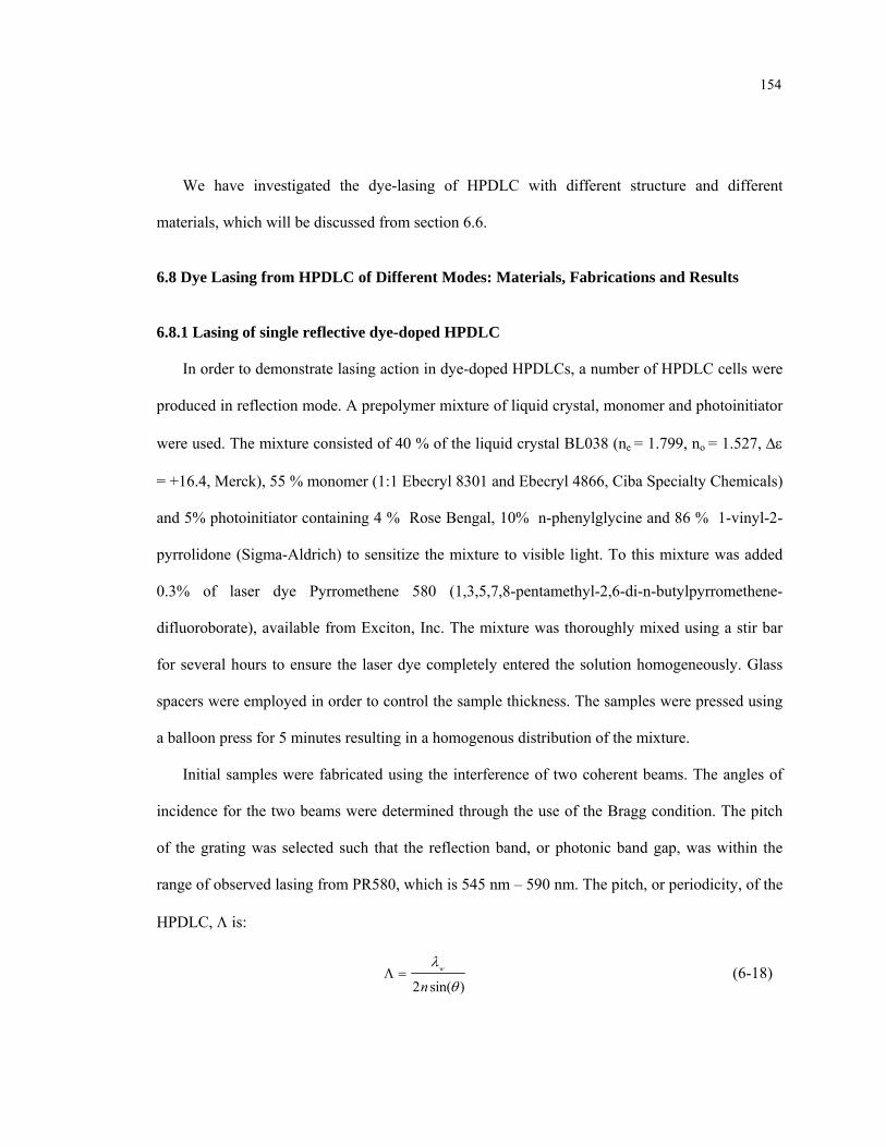
154
We have investigated the dye-lasing of HPDLC with different structure and different
materials, which will be discussed from section 6.6.
6.8 Dye Lasing from HPDLC of Different Modes: Materials, Fabrications and Results
6.8.1 Lasing of single reflective dye-doped HPDLC
In order to demonstrate lasing action in dye-doped HPDLCs, a number of HPDLC cells were
produced in reflection mode. A prepolymer mixture of liquid crystal, monomer and photoinitiator
were used. The mixture consisted of 40 % of the liquid crystal BL038 (ne = 1.799, no = 1.527, Δε
= +16.4, Merck), 55 % monomer (1:1 Ebecryl 8301 and Ebecryl 4866, Ciba Specialty Chemicals)
and 5% photoinitiator containing 4 % Rose Bengal, 10% n-phenylglycine and 86 % 1-vinyl-2-
pyrrolidone (Sigma-Aldrich) to sensitize the mixture to visible light. To this mixture was added
0.3% of laser dye Pyrromethene 580 (1,3,5,7,8-pentamethyl-2,6-di-n-butylpyrromethene-
difluoroborate), available from Exciton, Inc. The mixture was thoroughly mixed using a stir bar
for several hours to ensure the laser dye completely entered the solution homogeneously. Glass
spacers were employed in order to control the sample thickness. The samples were pressed using
a balloon press for 5 minutes resulting in a homogenous distribution of the mixture.
Initial samples were fabricated using the interference of two coherent beams. The angles of
incidence for the two beams were determined through the use of the Bragg condition. The pitch
of the grating was selected such that the reflection band, or photonic band gap, was within the
range of observed lasing from PR580, which is 545 nm – 590 nm. The pitch, or periodicity, of the
HPDLC, Λ is:
Λ =λw
2n sin(θ ) (6-18)

155
where λw is the wavelength of the laser used to write the HPDLC grating, θ is the angle of
incidence for the writing beams, n is the average index of refraction of the prepolymer mixture, in
the case of our prepolymer mixture n ≈ 1.55. Once fabricated, the PBG, or reflection band will
occur at a wavelength λr = 2nΛ. An angle of incidence for the writing beams of 52° will result in
a pitch Λ = 187.1 nm and a reflected band near λr = 580 nm, ideal for the laser dye Pyrromethene
580.
Fig. 6.9. Lasing emission from a reflection mode HPDLC (solid line) and transmission spectra of
the same sample (dotted line).
A Brilliant model frequency doubled Nd:YAG laser operating at 532 nm was used to pump
our HPDLCs. While the laser has a repetition rate of 10 Hz and a maximum output of 200 mJ
per pulse, the laser output was attenuated down to approximately 6 mJ per pulse in our
experiments. A laser line filter was placed between the lasing sample and the fiber spectrometer
to block all light below 540 nm and eliminate the pump laser in the measured spectra. The solid

156
line in Fig. 6.9 shows a strong laser line peaking at 556.7 nm with a full width at half maximum
(FWHM) of ~6.6 nm. The transmission spectrum of the sample is also shown as a dotted line in
the figure. The thickness of the sample is 20 µm. It is clear that lasing occurs at the edge of the
band gap, or reflection notch of the grating. The other notch in the transmission spectrum is due
to the absorption by the Rose Bengal used in the photoinitiator, and the absorption of laser dye.
In order to switch the sample, an external voltage of 1 kHz square wave was applied to the
sample. The voltages measured ranged from 0 V to 300 V. Lasing emission at 100 V increments
is shown in Fig. 6.10. The peak of lasing is located at 556.7 nm with a FWHM of 6.6 nm at a
voltage of 0 V applied to the sample; peak at 555.1 nm with a FWHM of 8.8 nm, at a voltage of
100 V; peak at 555.1 nm with a FWHM of 9.7 nm, at 200 V; and peak at 555.1 nm with a FWHM
of 10.0 nm, at 300 V. Higher voltages were not attempted as they would have shorted the HPDLC
and destroyed the grating.
Fig. 6.10. Switching of the dye lasing emission from a reflection mode HPDLC

157
6.8.2 Lasing of transmissive Dye-doped HPDLC
Transmission mode HPDLCs were made with a small doping concentration of the laser dye
Pyrromethene 580. Prepolymer mixtures consisting of the materials identical to the recipe used
for reflective dye-doped HPDLC were also used for these gratings, with 27.5 % Ebecryl 4866,
27.5 % Ebecryl 8301, 40 % BL038 liquid crystal and 5 % photoinitiator, all in weight percentage.
The photoinitiator contained 4 % Rose Bengal, 10% n-phenylglycine and 86 % 1-vinyl-2-
pyrrolidone. Three different mixtures were made, each with a different doping level of laser dye:
0.5, 1.0 and 2.0 %. The mixtures were mixed with a stir bar for more than 2 hours to ensure
homogeneity.
D y e - d o p e d H P D L C
C y l i n d r i c a l L e n s
F o c a l L e n s
P u m p L a s e r
L a s i n g E m i s s i o n
Fig. 6.11 Two lens were used to generate the vertical line across the HPDLC grating in
order to increase the area of the gain medium being pumped
The fabrication laser setup consisted of two beams from a Verdi frequency doubled Nd:YAG
laser (532 nm), each with a beam power of ~1 W. The beams were incident on opposite sides of
the sample with a half angle between the two beams of 46°. This angle is designed to generate a

158
pitch length of ~369 nm within the HPDLC, corresponding to a band gap around 1145 nm. A
second order gap exists at half this wavelength, ~572 nm. We expect lasing to occur on the blue
edge of the gap, or in the range of 550 nm – 565 nm. Samples were fabricated using 20 µm
spacers to maintain sample thickness. Exposures in the laser setup were carried out for 1 minute.
In the laser pumping setup, two lenses were placed between the pump laser and the lasing
sample. The first lens was a focal lens used to focus the pump beam down to a spot and then
expand the beam, the second was cylindrical lens used to transform the beam into a vertical line
across the HPDLC grating, increasing the area of the gain medium being pumped. The setup is
shown in Fig. 6.11. Lasing was measured from the edge of the sample, parallel to the grating
vector of the HPDLC. A fiber spectrometer with a resolution of ~2 nm was used for lasing
intensity measurement.
Unlike the reflective HPDLC in the previous section, lasing from the dye-doped transmissive
HPDLC is dependent on the polarization state of pump beam. For the convenience of discussion,
here we define the S-component of the pumping laser as the polarized component with
polarization direction parallel to the grating direction or lasing emission direction, the P-
component with polarization direction perpendicular to the grating direction. Measurements were
first made of the HPDLC sample with 0.5% dye concentration. Fig. 6.12 shows the emission as
the pump beam polarization is changed from linear s-polarized to linear p-polarized by rotating a
λ/2 waveplate 45° between the polarizer and the pumping laser. The polarizer is set with its
direction parallel to the grating direction of the HPDLC. The pumping light polarization
dependence of the lasing emission was also observed for the dye-doped HPDLC samples with
different concentrations (1% and 2%) of laser dye, which are shown in Fig. 6.13 and Fig. 6.14.

159
The phenomenon of the pumping light polarization dependence of the lasing emission can be
explained by the anisotropic alignment of he dye molecules inside the HPDLC, as we have
discussed in previous sections. Fig. 6.15 further illustrates the microstructure of the dye-doped
transmissive HPDLC system. While alternating liquid crystal-rich layers and polymer-rich layer
are generated during the polymerization process under the laser interference , the dye molecules
accumulate in the liquid crystal layer much more than in polymer layer and are aligned along the
direction of the liquid crystals, which, on average, is perpendicular to the grating direction. Thus
a p-polarized pump laser will generate much more lasing emission.
Lasing Vs Polarization State of Pumping Light (0.5% Dye Concentration)
0
2000
4000
60008000
10000
12000
14000
16000
545 547 549 551 553 555
Wavelength (nm)
Lasi
ng In
tens
ity
(Arb
. Uni
ts)
S-PolarizedP-Polarized
Fig. 6.12. Lasing emission of the sample with 0.5% Dye concentration as the pump beam
polarization is changed from s-polarized to p-polarization.
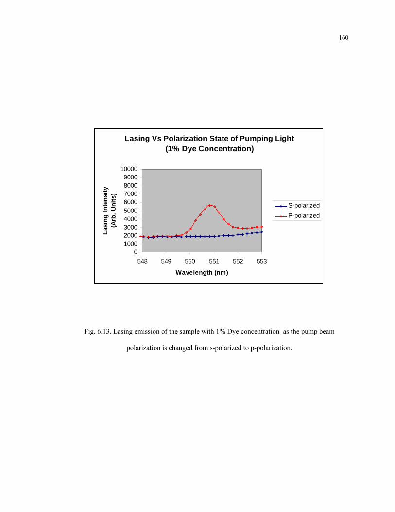
160
Lasing Vs Polarization State of Pumping Light(1% Dye Concentration)
0100020003000400050006000700080009000
10000
548 549 550 551 552 553
Wavelength (nm)
Lasi
ng In
tens
ity
(Arb
. Uni
ts)
S-polarizedP-polarized
Fig. 6.13. Lasing emission of the sample with 1% Dye concentration as the pump beam
polarization is changed from s-polarized to p-polarization.

161
Lasing Vs Polarization State of Pumping Light(2% dye concentration)
02000400060008000
100001200014000160001800020000
548 550 552 554 556 558
Wavelength (nm)
Lasi
ng In
tens
ity (A
rb. U
nits
)
S-polarizedP-polarized
Fig. 6.14. Lasing emission of the sample with 2% Dye concentration as the pump beam
polarization is changed from s-polarization to p-polarization.

162
Polymer layer LC layer: Dye : LC
P-polarized Pump Laser
S-polarized Pump Laser
Fig. 6.15. Dye molecules are distributed in the liquid crystal layers and are aligned with the
liquid crystal in the surface, and are perpendicular to the grating direction.
Measurements were also made to investigate the threshold nature of these samples, one of the
key features of a lasing system. The spectrum was acquired at increasing pump energies with
incident p-polarization, and the peak intensity was recorded for each spectrum. Fig. 6.16 and Fig.
6.17 show the intensities of lasing emission increase with the pumping energies, for dye-doped
HPDLC samples with dye concentration of 0.5% and 1%. It is apparent that the FWHM of the
lasing peak at around 551 nm is ~2 nm, at the minimum resolution of our spectrometer. The
emission peak grows significantly with increasing pump power. When the pumping energy
reaches the higher level, the lasing intensity is saturated. When the peak intensity is plotted as a
function of the pump energy, a threshold can be seen in the neighborhood of 18 µJ for the sample
with a dye concentration of 0.5%. Fig. 6.18 shows the emission intensity of the lasing peak at

163
various pump energies for the sample with a dye concentration of 0.5%. The threshold is
determined to be ~18 µJ.
Lasing Emission (0.5% dye concentration)
0
10000
20000
30000
40000
50000
60000
70000
546 548 550 552 554
Wavelength ( nm )
Lasi
ng In
tens
ity
(Arb
. Uni
ts)
9 Micro-J15.5 Micro-J21 Micro-J32 Micro-J44 Micro-J70 Micro-J
Fig. 6.16. Lasing emission at various pump energies in a sample with 0.5% dye concentration.

164
Lasing Emission (1% dye concentration)
0
5000
10000
15000
20000
25000
548 549 550 551 552 553
Wavelength ( nm )
Lasi
ng In
tens
ity (A
rb. U
nits
)
32 Micro-J44 Micro-J66 Micro-J77 Micro-J92 Micro-J120 Micro-J145 Micro-J200 Micro-J
Fig. 6.17. Lasing emission at various pump energies in a sample with 1% dye concentration.
Fig. 6.18. Peak emission intensity at various pump energies. A threshold is seen at ~18 µJ.
Sample has dye concentration of 0.5%.

165
Lasing at Various Voltages
0
1000
2000
3000
4000
5000
6000
7000
8000
9000
548 550 552 554
Wavelength (nm)
Lasi
ng In
tens
ity
(Arb
. Uni
ts) 0 v
50 v100 v200 v
Fig. 6.19. Effect of electric fields on lasing in a transmission mode HPDLC. Energy of Pumping
laser is 20 μJ.
The electro-optic response was observed for these lasing systems. An electric field was
applied across the sample doped with a 1.0 % laser dye. The applied voltage ranged from 0 V to
200 V. The measured spectra at 0 V, 100 V and 200 V are shown in Fig. 6.19.
We observe the emission falls off by a factor of two as a voltage of 200 V is applied across
the sample, as compared to the zero voltage case. The grating is essentially being switched off by
the electric field, allowing the refractive index of the liquid crystal droplets to be index matched

166
to that of the polymer. Further work is needed to optimize the materials, perfectly matching the
ordinary index of the liquid crystal and the index of the polymer.
6.8.3 Multiple-Method for Lasing Tuning
In order to tune the wavelength peak of the laser emission, several modes of operation are
proposed, as shown in Fig. 6.20. While Figures 6.20(a) and (b) show the basic principle of an
HPDLC as discussed before, Fig. 6.20(c) shows a three panel stack with a broad band incident
white light, ΔλW, and three reflection bands λB1, λB2, and λB3, whose peak wavelengths are
dictated by Bragg’s law, λB=2d<n> for normal incident light, where d is the plane thickness. This
is a very attractive approach to create a tunable laser element since the given Bragg reflection
band can be turned on or off electrically. Fig. 6.20(d) shows the structure of a chirped HPDLC,
where the reflected Bragg peak, λ(xi), is a function of the spatial position in the sample, x. A
chirped HPDLC is obtained by creating the interference pattern with diverging beams thereby
spatially changing the thickness of the Bragg planes, d, within the sample as a function of
position. Fig. 6.20(e) shows a single electrically tuned HPDLC, where the peak wavelength,
λ(Vi), can be tuned as a function of applied voltage.
While in Fig. 6.10 we have already shown the electrical tuning of the lasing peak, though the
tuning range is only ~ 1 nm, new configurations and materials are necessary to enable a larger
modulation of the refraction index of HPDLC, in order to expand the tunable range.
6.8.3.1 Lasing Tuning in Stack of HPDLCs
As a possibility for creating a tunable laser source, the stacked HPDLC configuration was
fabricated as shown in Fig. 6.20(c).

167
Fig. 6.20. Various modes of operation to tune the wavelength peak of the lasing.
Lasing Switching of HPDLC stack
0
500
1000
1500
2000
2500
3000
3500
540 560 580 600 620 640
Wavelength (nm)
Lasi
ng E
mis
sion
(A
rb. U
nits
)
0 V150 V250 V
Fig. 6.21. Stacked grating configuration for tunable lasing. The grating with the smaller pitch,
lower reflection band is in a zero voltage state, while the larger pitch grating has a field applied
across it to switch off lasing

168
Two HPDLCs doped with different laser dyes, at different pitches, were fabricated separately
using the procedures mentioned above and then sandwiched together. One cell contained the laser
dye Pyrromethene 580 and the other was doped with DCM; each cell was 10 µm thick. These
stacked cells were then placed in front of the pump beam and the lasing emission was observed
with the spectrometer. Two laser emission lines were observed. The solid line in Fig. 6.21 shows
the lasing emission when no voltage was applied. A field of increasing strength was applied
across one of the cells as the other was left in a zero field state, as shown by the dashed and
dotted lines in Fig. 6.21.
Transmission of HPDLC Gratings
0
20
40
60
80
100
120
540 560 580 600 620 640
Wavelength (nm)
Tran
smis
sion
(Arb
. Uni
ts)
Grating AGrating B
Fig. 6.22. Transmission of the two gratings used in the stack. Grating A is doped with dye
P580, and grating B is doped with dye DCM.

169
The spectral response of the two gratings of the stack were measured separately, as shown in
Fig. 6.22. Grating A is doped with dye P580, and grating B is doped with dye DCM. Comparing
Fig.s 6.21 and 6.22, it is clearly shown that the wavelength of the lasing emission of the left peak
(in Fig. 6.21) is located at the left edge of the reflection band in grating A, and the wavelength of
lasing emission of the right peak (in Fig. 6.21) is located at the left edge of the reflection band in
grating B.
We have demonstrated that the creation of stacked, dye-doped HPDLCs is a viable option for
multiple line lasing devices.
6.8.3.2 Lasing Tuning in Chirped HPDLC
Chirped HPDLCs with reflection bands ranging between 560 nm and 590 nm were
fabricated. The following formulation has been used for sample preparation: 55% homogeneous
prepolymer mixture composed of a photo-polymerizable urethane acrylate (from Ciba Specialty
Chemicals), 45% liquid crystal (BL038 from EM Industries, ne=1.799, no=1.527, Δε=+16.4) and
5% photoinitiator (Rose Bengal, n-phenylglycine, and 1-vinyl-2-pyrrolidone; all available from
Sigma-Aldrich). The mixture was placed between two AR-ITO coated glass substrates; glass
spacers were employed in order to control the sample thickness and the samples were pressed
using a balloon press for 5 minutes resulting in a homogenous distribution of the mixture.
Two additional lenses were used in the holographic writing system to generate a chirped
grating. These lenses, placed in the path of the split beams, created diverging beams that created
the spatially varying grating spacing within the sample. When tested with a spectrometer, a shift
in the location of the reflection notch of the transmission spectra was observed when the sample
was probed along one direction. Samples with shifts as high as 10 nm were fabricated. More
divergent beams and larger samples can be used to create larger shifts of the lasing peak.

170
Two lenses with focal lengths of 100 mm were used in our setup to create diverging beams at
the cell. The samples are exposed to a 532 nm Verdi laser for 30 seconds at a power of 2 W. An
Ocean Optics fiber spectrometer was used to measure the transmission of the formed grating
within the samples. A reflection notch varying as a function of position in the sample relative to
the spectrometer was observed in all of the samples made with a wavelength range between 560
nm and 590 nm. When measured at two opposite edges of the sample, a chirped HPDLCs has
reflection notches with minima in the transmission spectra between 562 nm and 572 nm. This
shift, at three spots in the transmission spectra, is seen in the top of Fig. 6.23.
These samples were pumped as described above; the lasing spectra were measured at the
same three spots and the resulting spectra are shown in the bottom of Fig. 6.23. Laser emission
appears at the edge of the band gap, or reflection band, for each point. The lasing peaks are
located at 554.4, 555.1, and 557.8 nm for the left, middle and right points, respectively. This
corresponds to approximately a 4 nm shift in the lasing wavelength. It is clear these grating
structures have spatial tunability.
In addition to this spatial tunability, lasing from each spot of these chirped dye-doped
HPDLCs are also switchable, as is seen in Fig. 6.24. The fields necessary for switching a chirped
HPDLC are comparable to those required for switching a non-chirped configuration. The peak of
laser emission is at 555.3 nm with a FWHM of 4.9 nm, at 0 V; the peak of laser emission is at
555.3 nm with a FWHM of 5.2 nm, at 100 V; the peak of laser emission is at 556.5 nm with a
FWHM of 7.0 nm, at 200 V,; the peak of laser emission is at 556.5 nm with a FWHM of 7.4 nm,
at 300 V.

171
Fig. 6.23. Tuning of a chirped HPDLC. Transmission spectra at left (solid), middle (dashed) and
right (dotted) points on the sample (top); and lasing emission at left (solid), middle (dashed) and
right (dotted) points on the sample (bottom).
Fig. 6.24. Switching of a reflection mode chirped HPDLC

172
6.9 Two Dimensional Dye-Doped HPDLC Lasing
2D structures in PDLC materials can be fabricated through multiple-beam holography. For N
linear polarized plane wave beams, the irradiance of the interference pattern can be expressed as:
])(exp[)(1
*
1rkkiEErI ij
N
ii
N
jj
rrrrvr−⋅= ∑ ∑
= =
(6-19)
If the reciprocal wave vectors ijji kkGrrr
−= form a reciprocal lattice, then the )(rI rhas a
period structure with the scale of lattice comparable to the wavelength of light. The ability to
manipulate the wave vectors and polarization directions allows for the design of 2D or even 3D
interference patterns [119-122].
We will discuss a 4-beam interference in details. The 4 beams are all of the same polar angle
θ, evenly distributed at Δφ = 90° intervals around the azimuth, and have the same intensity. For
simplicity, let us assume that 2 beams lie in the X-Z plane and have the polarization directions
along the Y direction, while the other 2 beams lie in the Y-Z plane and have a polarization
directions along the X direction.
The 4 beams can be analytically expressed as:
][ )()(01
tizkxkitizkxkiy eeeeEeE zxzx ωω +−−+ +=rr
,
][ )()(02
tizkxkitizkxkiy eeeeEeE zxzx ωω +−−−+− +=rr
,
][ )()(03
tizkykitizkykix eeeeEeE zyzy ωω +−−+ +=rr
,
][ )()(03
tizkykitizkykix eeeeEeE zyzy ωω +−−−+− +=rr
(6-20)
where xer and are two unit vector along X-axis and Y-axis directions. When the 4 beams meet,
the total electric field is:
yer

173
∑=
=4
1iiEErr
(6-21)
and
43212
42
32
22
12
4
1
2 22)( EEEEEEEEEEi
i
rrrrrrrrrr•+•++++== ∑
= (6-22)
Here, some terms, such as 31 EErr
• and 42 EErr
• , disappear because the polarization directions
are perpendicular, or . The total intensity is: 0=• yx ee vv
43212
42
32
22
12 22 EEEEEEEEEI
rrrrrrrrr•+•++++==
(6-23)
As 02
02
42
32
22
1 IEEEEE =====rrrr
and
][][22 )()()()(2021
tizkxkitizkxkitizkxkitizkxki eeeeeeeeEEE zxzxzxzx ωωωω +−−−+−+−−+ +•+=•rr
)2cos(4]2 20
2)2222220 xkEeeeeeeE x
tizkixkixkitizki zxxz =+++= −−− ωω (6-24)
Similarly,
)2cos(42 2043 ykEEE y=•
rr (6-25)
Thus the total intensity is:
)]2cos()2[cos(44 00 ykxkIII yx ++= (6-26)
Fig. 6.25(a) shows the structure of a 4-beam interference. As the polar angle of the 4 beams
are the same, we have )sin(2 θλπ
== yx kk , thus (6.26) generates a 2-dimentional square-
lattice with intensity modulation. Fig. 6.25(b) shows the resulting interference pattern as
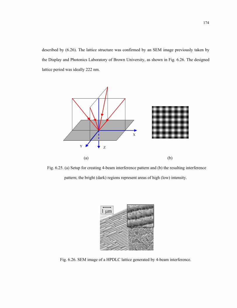
174
described by (6.26). The lattice structure was confirmed by an SEM image previously taken by
the Display and Photonics Laboratory of Brown University, as shown in Fig. 6.26. The designed
lattice period was ideally 222 nm.
X
Y Z
(a) (b)
Fig. 6.25. (a) Setup for creating 4-beam interference pattern and (b) the resulting interference
pattern; the bright (dark) regions represent areas of high (low) intensity.
Fig. 6.26. SEM image of a HPDLC lattice generated by 4-beam interference.

175
Another 2D configuration made use of 6 incident beams evenly distributed at Δφ = 60°
increments around the azimuth, each with the same polar angle and same intensity. The 6-beam
interference results in a 2D hexagonal lattice structure. The beam setup and the resulting
interference pattern are shown in Fig. 6.27.
Fig. 6.27. (a) Setup for creating a 6-beam interference pattern and (b) the resulting interference
pattern; the bright (dark) regions represent areas of high (low) intensity.
While these two configurations may not exhibit complete band gaps, band gaps do exist along
certain directions, along the unit vectors comprising the lattice, for instance; for this reason a
strong lasing intensity should be observed along these directions when lasing dye materials are
doped into the HPDLC.
We fabricated both 4- and 6-beam 2D dye-doped HPDLC grating structures using the optical
setup discussed above. The polar angles of incidence from the normal of the glass substrate were
θ = 10° for the 4- beams setup. From 6.19, we know the pitch of the 4-beam setup is decided by

176
Λ=)sin(2 θ
λππ==
yx kk=1532 nm, for the writing laser wavelength 532 nm and polar angle
θ=10°.
x
y
Fig. 6.28. (a) Isointensity plot for four-beam fabrication with directions of the band gap and
subsequently lasing; and (b) lasing from this structure doped with the laser dyes Pyrromethene
580 (solid line) and DCM (dotted line). Lasing emission is measured along x-direction.
The materials used in the fabrication of the 2-D dye-doped HPDLC are basically the same as
the mixtures in fabricating the 1-D samples. The prepolymer mixture consisted of 40 % of the
liquid crystal BL038 (ne = 1.799, no = 1.527, Δε = +16.4, Merck), 55 % monomer (1:1 Ebecryl
8301 and Ebecryl 4866, Ciba Specialty Chemicals) and 5% photoinitiator containing Rose
Bengal, n-phenylglycine and 1-vinyl-2-pyrrolidone (Sigma-Aldrich) to sensitize the mixture to
visible light. To this mixture was added 0.3% of one of the laser dyes Pyrromethene 580
(1,3,5,7,8-pentamethyl-2,6-di-n-butylpyrromethene-difluoroborate) or DCM (4-
Dicyanomethylene-2-methyl-6-p-diethylaminostyryl-4-H-pyran), both available from Exciton,

177
Inc. The mixture was thoroughly mixed using a stir bar for several hours to ensure the laser dye
completely entered the solution homogeneously.
In the 4-beam structure, a band gap is expected in x-direction, y-direction and diagonal
direction, as shown in Fig. 6.28(a). When viewed along these directions, the cross section of the
HPDLC sample will appear as a simple 1D grating structure, like that of the 1D gratings
fabricated previously. When measured from the x-direction (and the same for y-direction), laser
emission peaked at 558 nm with a FWHM of 5 nm (solid line) was observed in the sample doped
with dye Pyrromethene 580; lasing emission peaked at 614.3 nm with a FWHM of 12.2 nm
(dashed line) in the sample doped with the dye DCM. Both of the lasing emission results are
shown in Fig. 6.28(b).
Fig. 6.29. (a) Isointensity plot for six-beam fabrication with directions of band gap and
subsequently lasing; and (b) lasing from this structure doped with the laser dyes Pyrromethene
580 (solid line) and DCM (dotted line).

178
We also fabricated a 6-beam 2D dye-doped HPDLC grating structure using the optical setup
discussed in Fig. 6.27(a). The polar angles of incidence from the normal of the glass substrate
were θ = 27°.
The 6-beam structure contains three axes along which lasing is expected, as seen in Fig.
6.29(a). Laser emission of the sample doped with PM580 peaked at 554.5 nm, with a FWHM of
5.1 nm (solid line); Lasing of sample doped with DCM peaked at 613 nm, with a FWHM of 14.8
nm (dashed line), both are shown in Fig. 6.29(b). Comparable lasing was observed along all three
axes.
6.10 Lasing of Polarization Grating
In most applications of holography, the means of interference is the intensity interference, as
most holographic materials are sensitive to exposure intensity. Recently a few materials have
been found to be sensitive to the local polarization direction and intensity, and they have been
utilized to record the so-called polarization interference. The first demonstration of tan
interference pattern recorded using two orthogonally polarized beams was proposed by
Kalichashvili [123], and further configurations were systematically studied by Nikolova and
Todorov [124].
The interference of two orthogonally polarized beams gives a uniform intensity, however, the
distribution of the polarization direction is spatially modulated. Two special and interesting cases
are considered as shown in Fig. 6.30:
(1) Two beams are linearly polarized with orthogonal polarization directions (Fig. 6.30(a));
(2) Two beams are circularly polarized with opposite handedness, or one left-handed and the
other right handed. (Fig. 6.30(b))

179
For the two circularly polarized beams with different handedness, they can be described in
the Jones matrix method by: , and . Assuming there is no difference
of optical path length when the two beams meet at the point x = 0, then the difference of the
optical path (OPD) along the x-axis is decided by:
⎟⎟⎠
⎞⎜⎜⎝
⎛= 2/1
1πie
Er
⎟⎟⎠
⎞⎜⎜⎝
⎛= − 2/2
1πie
Er
)sin(2 θxOPD = , and the phase mismatch
Between the two beams is λ
θπ )sin(4 x=Δ , thus the total electric field is given by:
2/2/
2/
2/2/ 2)2/sin()2/cos(
)2/2/cos(2)2/cos(2(11 Δ
Δ
ΔΔ
− ⎟⎟⎠
⎞⎜⎜⎝
⎛ΔΔ
=⎟⎟⎠
⎞⎜⎜⎝
⎛
Δ−Δ
=⎟⎟⎠
⎞⎜⎜⎝
⎛+⎟⎟
⎠
⎞⎜⎜⎝
⎛= i
i
ii
ii ee
ee
eeE
πππ
r
Here it is interesting that the polarization states along the x-axis are all linearly polarized,
with periodic modulation of the polarization directions. Because of the fact that the polarization
states and are the same, the period along x axis is⎟⎟⎠
⎞⎜⎜⎝
⎛ba
⎟⎟⎠
⎞⎜⎜⎝
⎛−−
ba
)sin(22/ θλπ
=Δ
=Λ .
Similarly, considering the two linearly polarized beams with equal intensity, the total electric
field of interference is given by:
⎟⎟⎠
⎞⎜⎜⎝
⎛∝+= Δie
EEE1
21
rrr
Thus, the polarization is also modulated along the x-direction.
As the morphology of the liquid crystal system is easily controlled using surface alignment
and holographic techniques, liquid crystal and polymer can be utilized for polarization recordings
of polarization grating. The optically induced molecular reorientation in a nematic LC film has
been well studied both theoretically and experimentally. A linear photopolymerizable polymer
(LPP) was reported by Crawford’s group at Brown University to create a polarization grating on a
surface alignment layer for a nematic liquid crystal, which propagated into the bulk nematic
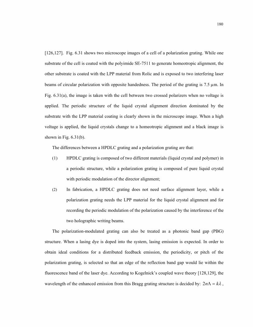
180
[126,127]. Fig. 6.31 shows two microscope images of a cell of a polarization grating. While one
substrate of the cell is coated with the polyimide SE-7511 to generate homeotropic alignment, the
other substrate is coated with the LPP material from Rolic and is exposed to two interfering laser
beams of circular polarization with opposite handedness. The period of the grating is 7.5 μm. In
Fig. 6.31(a), the image is taken with the cell between two crossed polarizers when no voltage is
applied. The periodic structure of the liquid crystal alignment direction dominated by the
substrate with the LPP material coating is clearly shown in the microscope image. When a high
voltage is applied, the liquid crystals change to a homeotropic alignment and a black image is
shown in Fig. 6.31(b).
The differences between a HPDLC grating and a polarization grating are that:
(1) HPDLC grating is composed of two different materials (liquid crystal and polymer) in
a periodic structure, while a polarization grating is composed of pure liquid crystal
with periodic modulation of the director alignment;
(2) In fabrication, a HPDLC grating does not need surface alignment layer, while a
polarization grating needs the LPP material for the liquid crystal alignment and for
recording the periodic modulation of the polarization caused by the interference of the
two holographic writing beams.
The polarization-modulated grating can also be treated as a photonic band gap (PBG)
structure. When a lasing dye is doped into the system, lasing emission is expected. In order to
obtain ideal conditions for a distributed feedback emission, the periodicity, or pitch of the
polarization grating, is selected so that an edge of the reflection band gap would lie within the
fluorescence band of the laser dye. According to Kogelnick’s coupled wave theory [128,129], the
wavelength of the enhanced emission from this Bragg grating structure is decided by: λkn =Λ2 ,

181
where n is an effective refractive index, Λ is the pitch of the periodic medium and k is an integer
representing the diffraction order of the grating.
We fabricated the dye-doped nematic liquid crystal samples with a polarization grating
structure as discussed. The LPP material (ROLIC) was spin-coated onto two glass substrates with
an anti-reflection coating on one side, a thin layer of index-matched indium tin oxide (ITO)
coating on the other. 5 µm fiber spacers were spread on one substrate and then the uniform empty
cells were assembled with epoxy. These samples were then exposed to an interference pattern
generated by two circularly polarized beams of identical intensity and opposite handedness, from
an Ar+ laser operating at 351 nm. Each beam contained a power of approximately 40 mW. The
exposure time was about 30 seconds. Under the ultraviolet radiation of these two interfering
beams, the LPP molecules polymerize with their molecular axes parallel to the local polarization
direction that was periodically modulated as shown in Fig. 6.30(b).
The nematic liquid crystal BL038 (ne = 1.7999, no = 1.527, Δε = +16.4, EM Industries) was
chosen, for its large birefringence and dielectric anisotropy, as the host solvent for an organic
laser dye Pyrromethene 580 (PM580, Exciton, Inc.). The concentration of the dye was ~ 0.5 wt.-
%. The dye-doped liquid crystal mixture was mixed for approximately one hour using a stir bar to
ensure a homogeneous mixture, before being capillary filled into the exposed cells.
These samples were pumped using a 532 nm frequency doubled Nd:YAG laser (Quantel)
with pulse widths of 9 ns, a repetition rate of 10 Hz and a variable beam intensity. The incident
angle of pumping beam on the sample is set at approximately 45°. The emission from the sample
was measured from the edge of the grating, as shown in Fig. 6.32(b). Two lenses were used to
focus the incident beam on the grating structure; a plano-convex lens focuses the incident beam to
a point and a cylindrical lens spreads the beam along a direction parallel to the grating vector of

182
the structure. This setup increases the area of region excited by the pump beam within the grating
structure, as is shown in Fig. 6.11.
Laser emission from these samples was measured and is shown in Fig. 6.33. The lasing
emission peak has a full width half maximum (FWHM) of ~5 nm, compared with that of the
FWHM of the fluorescence band (>50 nm).
(a)
(b)
xz
y
2θ
xz
y
2θ
E1
E2
E1
E2
xx
xx
Fig. 6.30. (a) Two linearly polarized beams with orthogonal polarization directions; (b)Two
circularly polarized beams with opposite sense of clockwise. [127].

183
(a) (b)
Fig. 6.31. Microscope images of a cell of polarization grating between two crossed polarizers. (a)
no voltage is applied; (b) 20 V voltage is applied.
Fig. 6.32. Writing beam and pump beam for fabrication and lasing emission testing of the
polarization gratings.

184
Fig. 6.33. Lasing emission from a liquid crystal polarization holography grating.
Fig. 6.34. Threshold of laser emission for the dye-dope liquid crystal polarization grating.

185
The threshold of these samples was measured and is shown in Fig. 6.34. The threshold pump
energy is ~ 225 µJ. Below this threshold point, the lasing emission energy changes slowly
relative to the rate of change of pump energy. Above this threshold point, the rate of change
increases more drastically. The FWHM of emission drops down to ~5 nm under a 700 µJ pump
beam.
Also measured was the pump beam polarization dependence of these grating structures. A
half-wave plate was placed after the polarizer in front of the pumping laser. The rotation of the
polarization was controlled by the rotation of a half wave plate. A 50% increase in lasing
emission was observed, as shown in Fig. 6.35, when the incident polarization state was rotated
from s- polarization to p-polarization. As we have discussed in the lasing of transmissive HPDLC
gratings, dye molecules tend to align themselves along with the liquid crystals. In the structure of
the polarization grating, the surface alignment directions of the liquid crystal rotate within the
plane of the substrates along with the modulation of the polarization directions. When the pump
laser is at normal incidence, both the p-polarized beam and the s-polarized beam are identical to
the dye molecules that have a uniform sinusoidal distribution in different in-plane directions.
However, when the incident angle of the pump beam is 45°, the electric field of the p-polarized
light still lies in plane, while that of s-polarized light has only 50% that lies in plane, the other
50% has the electric field perpendicular to the plane of the liquid crystals and the dye molecules
make little contribution to the lasing emission.
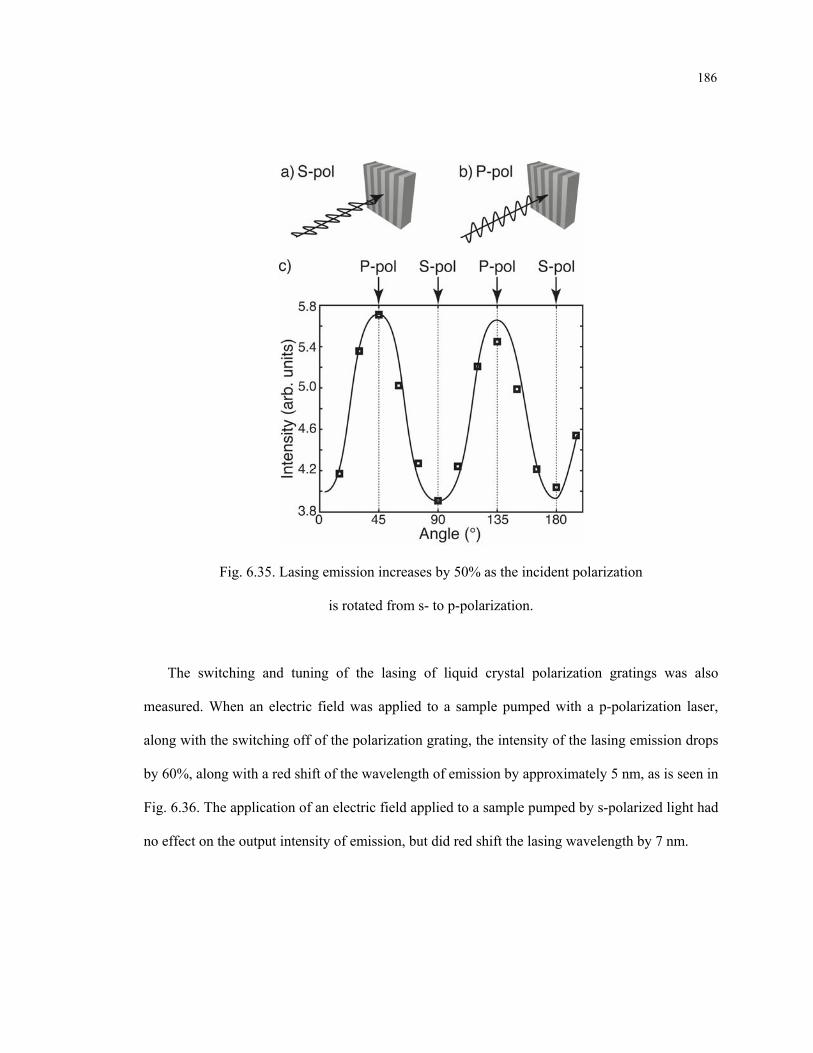
186
Fig. 6.35. Lasing emission increases by 50% as the incident polarization
is rotated from s- to p-polarization.
The switching and tuning of the lasing of liquid crystal polarization gratings was also
measured. When an electric field was applied to a sample pumped with a p-polarization laser,
along with the switching off of the polarization grating, the intensity of the lasing emission drops
by 60%, along with a red shift of the wavelength of emission by approximately 5 nm, as is seen in
Fig. 6.36. The application of an electric field applied to a sample pumped by s-polarized light had
no effect on the output intensity of emission, but did red shift the lasing wavelength by 7 nm.

187
Fig. 6.36. Effect of an applied electric field on a liquid crystal polarization grating
pumped by p-polarized light.

188
6.11 Summary and Conclusions
We have investigated the materials, fabrication and characterization of lasing emission of dye
doped HPDLCs. Lasing from different modes of HPDLCs has been studied, with a lasing peak
resolution of ~ 2 nm. Both the switching and tunability of the lasing function were demonstrated.
The research illustrates a potential for making electrically tunable lasers. Lasing from two-
dimensional HPDLC based photonic band gap (PBG) materials was also demonstrated. Finally,
lasing from polarization modulated gratings was investigated.

CHAPTER 7
Conclusions and Considerations on Future Work
Several innovative wavelength tunable devices based on liquid crystal technology, especially
on Holographic Polymer Dispersed Liquid Crystals (HPDLC) have been developed.
Based on the electrically controllable beam steering capability of transmission mode
HPDLCs, the concept and design of novel switchable circular to point converter (SCPC) devices
have been demonstrated for selecting and routing the wavelength channels discriminated by a
Fabry-Perot interferometer, with applications in Lidar detection, spectral imaging and optical
telecommunication. SCPC devices working at different wavelengths (visible and NIR) with
different channel numbers (single channel, 10-channel, and 32-channel) were fabricated and
investigated. Two types of SCPC devices were analyzed with more focus on the second type, a
beam-steering SCPC. A high diffraction efficiency of up to 80% in the visible, and 60% in the
NIR was achieved. The wavelength dependence and angular dependence were also investigated.
A random optical switch was proposed by integrating a Fabry-Perot interferometer with a stack of
SCPC units. The research on SCPC devices gives a potential for making electrically tunable
optical devices such as random optical switches and spectral imaging detectors.
Liquid crystal Fabry-Perot products were analyzed, fabricated and characterized for their
application in both spectral imaging and optical telecommunications. Both single-etalon systems
and twin-etalon systems were fabricated. Finesse value of more than 10 at the visible wavelength
range and finesse value of more than 30 in the NIR are achieved for the tunable LCFP product.
The materials, fabrication and characterization of lasing emission of dye doped HPDLCs was
also investigated. Lasing from different modes of HPDLCs has been demonstrated, with a lasing
189

190
peak resolution of up to 2 nm, and both the switching and tunability of the lasing function was
demonstrated. Lasing from two-dimensional HPDLC based photonic and gap (PBG) materials
was also studied. Finally, lasing from polarization modulated gratings was investigated.
In the future we will continue all of the research work based on HPDLC.
Considering the combination of dye-lasing with SCPC technology, one interesting research
topic would be a SCPC based dye-laser with an automatic focusing effect that may route all of the
laser signals to the focusing point, with the similar design of focusing SCPC.
Based on all of the switchable and wavelength-variable HDPLC devices, SCPC devices, and
dye-lasing devices that we have discussed, with more research work on different combinations of
materials, we would like to predict and further investigate a wavelength-tuning device by
electrical-tuning. In Fig. 3.8 we have discussed some of the previous work of the Display and
Photonics Laboratory at Brown University, where they used a polymer material with the
refraction index between the value of (ordinary refraction index of liquid crystal) and
(extraordinary refraction index of liquid crystal), which can be summarized as < < , for
the optical positive material satisfying < . When a polymer material is chosen with its
refraction index satisfying either < < or > > , then the external field will never
change the mismatch condition of the polymer layer and liquid crystal layer inside the HPDLC,
however, as the average refraction index of liquid crystal layer,
pn on en
on pn en
on en
pn on en pn en on
n , is tuned by the voltage, or
n = n (v), the center wavelength of the HPDLC grating, λ, can also be tuned based on the grating
equation at the normal incidence: λmdndn pplc =+ )(2 , where and are the thickness of
the liquid crystal layer, and polymer layer, respectively.
lcd pd

Bibliography
1. G. Friedel, Ann. Phys., 18, 273 (1992)
2. V. Tsvetkov, Acta Physicochim. (USSR) 16, 132 (1942)
3. Peter-Palffy Muhoray, Notes of Liquid Crystal Physics in Kent satate University
4. P. M. Chaikin and T. C. Lubensky, Principles of condensed matter physics, Chapter 6,
University Press, Cambridge, (1998)
5. C.Oseen, Trans. Faraday Soc., 29, 883(1933)
6. H. Zocher, Trans. Faraday Soc., 29, 945(1933)
7. F. C. Frank, Discuss. Faraday Soc. 25, 19 (1958)
8. M.C. Mauguin, Sur les cristaux liquides de Lehmann, Bull. Soc. Fr. Miner.,
34, 71-85 (1911)
9. D. Shenoy and K. Grueneberg and J. Naciri and R. Shashidhar, Photo-dimerized monolayer
(PDML) versus rubbed polyimide (RPI): A comparison of electro-optic properties, JPN. J.
APPL. PHYS., 37, 11A, L1326-L1329 (1998).
10 L.T. Creagh and A.R. Kmetz, Mechanism of surface alignment in nematic liquid crystal,
MOL. CRYST. LIQ. CRYST., 24, 58, (1973).
11. F. J. Kahn, Electric-field-induced color changes and pitch dilation in cholesteric liquid
crystals, PHYS. REV. LETT, 24, 5, 209-212 (1970).
12. A. Rapini and M.J. Papoular, J. Phys. (Paris), Colloq. C4, 30, C4-54 (1969).
13. M. G. Tomilin, Interaction of liquid crystals with a solid surface, J. Opt. Technol., 64, 5, 452-
475 (1997).
14. J. D. Jackson, Classical Electrodynamics (Wiley, New York, 1999).
191
192
15. D. W. Berreman, J. Opt. Soc. Am., 62, 502 (1972).
16. P. Yeh and C. Gu, Optics of Liquid Crystals,(John Wiley & Sons, New York, 1999).
17. H. Kogelnik, Coupled wave theory for thick hologram gratings, Bell Syst. Tech. J., 48,
2909-2947 (1969).
18. D. Gabor, A new microscopic principle, Nature, 161, 777-778 (1948).
19. D. Gabor, Microscopy by reconstructed wavefronts, Proceedings of the Royal Society A,
197, 454-487 (1949).
20. E. N. Leith and J. Upatnieks, Reconstructed wavefronts and communication theory, J. Opt.
Soc. Am., 52, 1123-1130 (1962).
21. J.D. Margerum, A.M. Lackner, E. Ramos, G. Smith, N.A.Vaz, J.L. Kohler, C.R. Allison,
Polymer dispersed liquid crystal film devices, and method of forming the same, US patent
4938568 (1990).
22. R. L. Sutherland and L. V. Natarajan and V. P. Tondiglia and T.J. Bunning, “Bragg gratings
in an acrylate polymer consisting of periodic polymer-dispersed liquid-crystal planes”,
Chem. Mater. , 5, 1533-1538 (1993).
23. K. Tanaka and K. Kato and S. Tsuru and S. Sakai, “A liquid crystal/polymer optical device
formed by holography for reflective color display applications”, SID Digest, 24, 109-111
(1993).
24. K. Tanaka and K. Kato and M. Date, “Fabrication of holographic polymer-dispersed liquid
crystal (HPDLC) with high reflectio efficiency”, JPN. J. APPL. PHYS., 38, L277-L278
(1999).
25. C. C. Bowley and G. P. Crawford, “Improved reflective displays based on polymer
dispersed liquid crystals”, J. Opt. Technol., 67, 717-722 (1999).

192
26. R. Smith and M. Popovich, “Application-specific integrated filters for color sequential
microdisplay-based projection applications”, Journal of SID, 9, 203-244 (2000).
27. S. Qian and J. Colegrove and P.-Y. Liu and X. Quan, Organic based electrically switchable
Bragg gratings and their aplications in photonics and telecommunications, Organic Photonic
Materials and Devices III, Vol 4279, Proc. SPIE, 69-77 (2001).
28. K. K. Vardanyan and J. Qi and J. N. Eakin and M. De Sarkar and G. P. Crawford, “Polymer
scaffolding model for holographic polymer-dispersed liquid crystals”, APPL. PHYS. LETT,
81, 4736-4738 (2002).
29. M. Jazbinsek, ID Olenik, M. Zgonik, AK Fontecchio,. GP Crawford, Characterization of
holographic polymer dispersed liquid crystal transmission gratings, J.Appl. Phys. 90, 3831-
3837 (2001).
30. Y. Boiko and J. N. Eakin and J. Vedrine and and G. P. Crawford, “Polarization-selective
switching in holographically formed polymer dispersed liquid crystals”, Opt. Lett., 27, 19,
1717-1719 (2002).
31. C. C. Bowley, P. A. Kossyrev, G. P. Crawford and S. Faris, Variable-wavelength switchable
Bragg gratings formed in polymer-dispersed liquid crystals, Appl. Phys. Let., 79, 1, 9-11
(2001).
32. K. Amundson and A. van Blaaderen and P. Wiltzius, Morphology and electro-optic
properties of polymer-dispersed liquid-crystal films, PHYS. REV. E, 55, 1646-1654 (1997).
33. M. de Sarkar and N. L. Gill and J. B. Whitehead and G. P. Crawford, “Effect of monomer
functionality on morphology and performance of the holographic transmission gratings
recorded on polymer dispersed liquid crystals”, Macromolecules, 36, 630-638 (2003).
34. M. de Sarkar and J. Qi and G.P. Crawford, “Influence of partial matrix fluorination on
morphology and performance of HPDLC transmission
192
gratings”, Polymer, 43, 26, 7335-7344 (2002).
35. P.G. Seybold, M. Gouterman, and J. Callis, Calorimetric, photometric and lifetime
determinations of fluorescence yields of fluorenscein dyes, Photochem. And Photobio., 9,
229-242 (1969).
36. C.C. Bowley, A.K. Fontecchio, G.P. Crawford, and H. Yuan, Electro-optic investigations of
HPDLCs: the effect of monomer functionality on display performance, Sco. Inf. Disp. Dig.,
XXX, 958-961 (1999).
37. C. Fabry and A. Perot, Ann. Chim. Phys., 16, P115 (1899).
38. M. Born and E. Wolf, Principles of Optics, 6th edition, Chapter 7, University Press,
Cambridge, (1980).
39. R. Ramaswami, K.N. Sivarajan, Optical Networks: A Practical Perspective, Morgan
Kaufmann Publisher, San Francisco, USA (1998).
40. Nakamura, Kiyoshi, Kurosawa, Yoko, Ishikawa, Kazuo, Tunable Optical Filters using a
LiNbO3 torsional actuator with a Fabry-Perot etalon, Applied Physics Letters, 68, 2799-
2800, (1996).
41. Reay, N K; Ring, J; Scaddan, R J, A tunable Fabry-Perot Filter for the visible, Journal of
Physics E: Scientific Instruments, Vol 7, August (1974).
42. M. Iodice, G. Cocorullo, F.G. Della Corte, I. Rendina, Silicon Fabry-Perot Filter for WDM
system systems channels monitoring, Optics Communications 183, 415-418 (2000).
43. M. W. Maeda, J.S. Patel, C. Lin, R. Spicer, J. Horrobin, Electronically tunable liquid-
crystal-etalon filter for high-density WDM systems, IEEE Photonics Technology Letters, 2,
820-822 (1990).

192
44. J.S. Patel; S. Jayantilal, Tunable liquid crystal etalon filter, US patent 5,150,236 (1992).
45. Hirabayashi, Katsuhiko, Tsuda, Hiroyuki, Kurokawa, Takashi, Liquid crystal Fabry-Perot
etalon with glass space, US patent 5,321,539 (1994).
46. Y. Bao, A. Sneh, K. Hsu, K.M. Johnson, J-Y. Liu, C.M. Miller, Y. Monta, M.B. McClain,
Photonics Technology Letters, IEEE, 8, 9, 1190-1192 (1996).
47. J.S. Patel; S. Jayantilal, Electronically tunable polarization-independent liquid crystal optical
filter, US patent 5,068,749 (1991).
48. J. Noto, K.E. Schneller, W.J. Schneller, R.B. Kerr, R.A. Doe, Nematic Fabry-Perot Etalons
for Ground and Space Based Atmospheric Remote Sensing, SPIE Proc., 3118, 368 – 377
(1997).
49. R.B. Kerr, Filters Expand Capabilities of Infrared Imaging, Laser Focus World, 151-158,
(2001).
50. Peter J. Collings and Jay S. Patel, Handbook of liquid crystal research, Chapter 12, Oxford
University Press, (1997).
51. Timothy L. Killeen, B.C. Kennedy, P.B. Hays, D.A. Symanow, and D. H. Ceckowski,
Image Plane Detector for the Dynamics Explorer Fabry-Perot Interferometer, Applied
Optics, V22, #22, 3503-3513 (1983).
52. Bissonnette; Luc R. Multiple scattering technique (MUST) lidar, US patent 5,239,352
(1993).
53. D. L. Hutt, L. R. Bissonnette, and L. Durand, Multiple field of view Lidar returns from
atmospheric aerosols, Applied Optics, Vol. 33, No. 12, 2338-2348 (1994).
54. Paul B., Hays, Circle to line interferometer optical system, Applied Optics, vol. 29, No. 10,
1482-1489 (1990).

192
55. Paul B., Hays, Circle-to-Line Interferometer Optical System, US patent 4,893,003 (1990).
56. M.J. McGill, W.R. Skinner and T.D. Irgang, Validation of wind profiles measured using
incoherent Doppler lidar. Appl. Opt., 36, 1928-1939 (1997).
57. M.J. McGill and R. Richard, Holographic optics convert rings to points for detection, Laser
Focus World, March (2001).
58. M.J. McGill, V.S. Scott, M. Marzouk, Apparatus and method using a holographic optical
element for converting a spectral distribution to image points, US patent 6313908 (2001).
59. H. Zhang and Y. Betremieux and J. Noto and R.B. Kerr, “Novel tunable liquid crystal
Fabry-Perot filters for fiber optical system”, Proceedings of SPIE, 4383,64-72 (2001).
60. H. Zhang and J. Qi and S. Watchorn and Y. Betremieux and G. P. Crawford and J. Noto and
R.B. Kerr, Novel switchable circular-to-point converter for lidar dectection, Proceedings of
the SPIE, Volume 5270, 199-207 (2004).
61. J. Noto, H.Zhang, Y.Betremieux, R.B. Kerr, M. Dorin, Narrow-band tunable filter for
remote sensing and hyper-spectral imaging, Proceedings of SPIE Vol. 4881, (2002).
62. J. Noto, Y.Betremieux, R.B. Kerr, H. Zhang, M. Taylor, S. Watchorn, M. Dorin, Tandem-
Etalon tunable filter for NIR spectral imaging, Proceedings of the SPIE, Volume 5157, 178-
189 (2003).
63. A. K. Richter and F. P. Carlson , Holographically Generated Lens, Applied Optics, vol. 13,
No. 12, 2924-2930 (1974).
64. M. Born and E. Wolf, Principles of Optics, 6th edition, Chapter 1, University Press,
Cambridge, (1980).
65. B. Bahadur, Liquid Crystals Applications and Uses, Vol. 3, World Scientific (1992).
66. P. W. Milonni, J. H. Eberly, Lasers, Chapter 13, John Wiley & Sons (1988).

192
67. Y. Huang, Y. Zhou, Q. Hong, A. Rapaport, M. Bass, S-T. Wu, Incident angle and
polarization effects on the dye-doped cholesteric liquid crystal laser, Opt. Comm., 261, 91-
96 (2006).
68. J.D. Joannopoulos, R. D. Meade, and J. N. Winn, Photonic Crystals: Molding the Flow of
Light, Princeton University Press, MA (1995).
69. K. Sakoda, Optical Properties of photonic crystals, Springer Series in Optical Sciences, Vol.
80, Springer, Berlin (2001)
70. E. Yablonovitch, Phys. Rev. Lett., 58, 2486 (1987).
71. J.D. Joannopoulos, P.R. Villeneuve, S. Fan, Photonic Crystals, Solid State Commun., 102,
165 (1997).
72. V. Berger, O. GauthierLafaye, and E. Costard, "Fabrication of a 2D photonic bandgap by a
holographic method," Electronics Letters 33, 425-426 (1997).
73. C. C. Cheng, A. Scherer, V. ArbetEngels, and E. Yablonovitch, "Lithographic band gap
tuning in photonic band gap crystals," Journal of Vacuum Science & Technology B 14,
4110-4114 (1996).
74. C. C. Cheng and A. Scherer, "Fabrication of photonic band-gap crystals," Journal of
Vacuum Science & Technology B 13, 2696-2700 (1995).
75. M.C. Wanke, Olaf Lehmann, Kurt Müller, Qingzhe Wen, Michael Stuke, Laser Rapid
Prototyping of Photonic Band-Gap Microstructures, Science Vol. 275. no. 5304, 1284 –
1286, (1997).
76. A. Imhof and D.J. Pine, Ordered Macroporous Materials by Emulsion Templating, Nature,
389, 948 (1997).
77. A.M. Urbas , M. Maldovan, P. DeRege, E.L. Thomas, Bicontinuous Cubic Block Copolymer
Photonic Crystals, Advanced Materials, Volume 14,

192
Issue 24 , 1850 – 1853 (2001).
78. S.A. Jenekhe, X.L. Chen, Mobility in Polycrystalline Oligothiophene Field-Effect
Transistors Dependent on Grain Size, Science, 283, 372. (1999).
79. W. Zhou, S.M. Kuebler, K.L. Braun, T. Yu, J.K. Cammack, C.K. Ober, J.W. Perry, and S.R.
Marder, Two-photon polymerization initiators for three-dimensional optical data storage and
microfabrication, Science, 296, 1106-1109 (2002).
80. J. P. Dowling, M. Scalora, M. J. Bloemer, and C. M. Bowden, The Photonic Band-Edge
Laser - a New Approach to Gain Enhancement, Journal of Applied Physics 75, 1896-1899
(1994).
81. A. Y. G. Fuh, T. H. Lin, J. H. Liu, and F. C. Wu, "Lasing in chiral photonic liquid crystals
and associated frequency tuning," Optics Express 12, 1857-1863 (2004).
82. T. Matsui, R. Ozaki, K. Funamoto, M. Ozaki, and K. Yoshino, "Flexible lasers made from
cholesteric liquid crystal polymers," Molecular Crystals and Liquid Crystals 413, 2643-2650
(2004).
83. M. F. Moreira, I. C. S. Carvalho, L. C. G. Valente, P. Palffy-Muhoray, B. Taheri, and A. F.
Munoz, "Fiber coupled cholesteric liquid crystal laser," Brazilian Journal of Physics 32, 455-
457 (2002).
84. A. Munoz, P. Palffy-Muhoray, and B. Taheri, "Ultraviolet lasing in cholesteric liquid
crystals," Optics Letters 26, 804-806 (2001).
85. J. Schmidtke, W. Stille, H. Finkelmann, and S. T. Kim, "Laser emission in a dye doped
cholesteric polymer network," Advanced Materials 14, 746-+ (2002).
86. P. V. Shibaev, R. L. Sanford, D. Chiappetta, V. Milner, A. Genack, and A. Bobrovsky,
"Light controllable tuning and switching of lasing in chiral liquid crystals," Optics Express
13, 2358-2363 (2005).

192
87. M. Kasano, M. Ozaki, K. Yoshino, D. Ganzke, and W. Haase, "Electrically tunable
waveguide laser based on ferroelectric liquid crystal," Applied Physics Letters 82, 4026-
4028 (2003).
88. M. Ozaki, M. Kasano, D. Ganzke, W. Haase, and K. Yoshino, "Mirrorless lasing in a dye-
doped ferroelectric liquid crystal," Advanced Materials 14, 306-+ (2002).
89. P. A. Bermel and M. Warner, "Photonic band structure of cholesteric elastomers," Physical
Review E 65, - (2002).
90. H. Finkelmann, S. T. Kim, A. Munoz, P. Palffy-Muhoray, and B. Taheri, "Tunable
mirrorless lasing in cholesteric liquid crystalline elastomers," Advanced Materials 13, 1069-
+ (2001).
91. P. V. Shibaev, V. I. Kopp, and A. Z. Genack, "Photonic materials based on mixtures of
cholesteric liquid crystals with polymers," Journal of Physical Chemistry B 107, 6961-6964
(2003).
92. J. A. Firehammer, N. M. Lawandy, and G. P. Crawford, "Lasing pixels: a new application
for polymer dispersed liquid crystals (PDLCs)," Molecular Crystals and Liquid Crystals
Science and Technology Section a-Molecular Crystals and Liquid Crystals 331, 2025-2032
(1999).
93. D. E. Lucchetta, L. Criante, O. Francescangeli, and F. Simoni, "Light amplification by dye-
doped holographic polymer dispersed liquid crystals," Applied Physics Letters 84, 4893-
4895 (2004).
94. V. K. S. Hsiao, C. G. Lu, G. S. He, M. Pan, A. N. Cartwright, P. N. Prasad, R. Jakubiak, R.
A. Vaia, and T. J. Bunning, "High contrast switching of distributed-feedback lasing in dye-
doped HPDLC transmission grating structures," Optics Express 13, 3787-3794 (2005).
192
95. R. Jakubiak, L. V. Natarajan, V. Tondiglia, G. S. He, P. N. Prasad, T. J. Bunning, and R. A.
Vaia, "Electrically switchable lasing from pyrromethene 597 embedded holographic-
polymer dispersed liquid crystals," Applied Physics Letters 85, 6095-6097 (2004).
96. P. G. de Gennes and J. Prost, The Physics of Liquid Crystal, Chapter 6, Oxford University
Press, New York, (1993).
97. L.S. Golderberg and J.M. Schnur, Tunable internal feedback liquid crystal laser, U.S. Patent
3,771,065 (1973).
98. I. P. Il'chishin, E. A. Tikhonov, V. G. Tishchenko, and M. T. Shpak, "Generation of a
tunable radiation by impurity cholesteric liquid crystals," JETP Lett. 32, 24-27 (1980).
99. E. Yablonovitch, Photonic Band-Gap Structures, Journal of the Optical Society of America
B-Optical Physics 10, 283-295 (1993).
100. V. I. Kopp, B. Fan, H. K. M. Vithana, and A. Z. Genack, "Low-threshold lasing at the edge
of a photonic stop band in cholesteric liquid crystals," Optics Letters 23, 1707-1709 (1998).
101. V. I. Kopp, Z. Q. Zhang, and A. Z. Genack, "Lasing in chiral photonic structures," Progress
in Quantum Electronics 27, 369-416 (2003).
102. A. Chanishvili, G. Chilaya, G. Petriashvili, R. Barberi, R. Bartolino, G. Cipparrone, A.
Mazzulla, R. Gimenez, L. Oriol, and M. Pinol, "Widely tunable ultraviolet-visible liquid
crystal laser," Applied Physics Letters 86, - (2005).
103. A. Chanishvili, G. Chilaya, G. Petriashvili, R. Barberi, R. Bartolino, G. Cipparrone, A.
Mazzulla, and L. Oriol, "Phototunable lasing in dye-doped cholesteric liquid crystals,"
Applied Physics Letters 83, 5353-5355 (2003).
A. Chanishvili, G. Chilaya, G. Petriashvili, R. Barberi, R. Bartolino, G. Cipparrone, A. Mazzulla,
and L. Oriol, "Lasing in dye-doped cholesteric liquid crystals: Two new tuning strategies,"
Advanced Materials , 16, 791-+ (2004).

192
104. Heino Finkelmann, Sung Tae Kim, Antonio Muæoz,. Peter Palffy-Muhoray, and Bahman
Taheri, Tunable Mirrorless Lasing in Cholesteric Liquid Crystalline Elastomers, Advanced
Materials, Volume 13, Issue 14 , 1069 – 1072 (2001).
105. A. Chanishvili, G. Chilaya, G. Petriashvili, R. Barberi, G. Cipparrone, A, Mazzulla and L.
Oriol, Lasing in dye-doped cholesteric liquid crystals: two new tuning strategies, Advanced
Materials, 16, 791-795, (2004).
106. A. Chanishvili, G. Chilaya, G. Petriashvili, R. Barberi, R. Bartolino, G. Cipparrone, A.
Mazzulla, R. Gimenez, L. Oriol, and M. Pinol, Widely tunable ultraviolet-visible liquid
crystal laser, Applied Physics Letters 86, 051107 (2005).
107. R. Jakubiak, T. J. Bunning, R. A. Vaia, L. V. Natarajan, and V. P. Tondiglia, "Electrically
switchable, one-dimensional polymeric resonators from holographic photopolymerization: A
new approach for active photonic bandgap materials," Advanced Materials 15, 241-+
(2003).
108. G. S. He, T. C. Lin, V. K. S. Hsiao, A. N. Cartwright, P. N. Prasad, L. V. Natarajan, V. P.
Tondiglia, R. Jakubiak, R. A. Vaia, and T. J. Bunning, "Tunable two-photon pumped lasing
using a holographic polymer-dispersed liquid-crystal grating as a distributed feedback
element," Applied Physics Letters 83, 2733-2735 (2003).
109. T. Matsui, M. Ozaki, and K. Yoshino, "Electro-tunable laser action in a dye-doped nematic
liquid crystal waveguide under holographic excitation," Applied Physics Letters 83, 422-424
(2003).
110. T. Matsui, M. Ozaki, and K. Yoshino, "Single-mode operation of electrotunable laser in a
dye-doped nematic liquid-crystal waveguide under holographic excitation," Japanese Journal
of Applied Physics Part 2-Letters 42, L1462-L1464 (2003).
192
111. D. E. Lucchetta, L. Criante, O. Francescangeli, and F. Simoni, "Wavelength flipping in laser
emission driven by a switchable holographic grating," Applied Physics Letters 84, 837-839
(2004).
112. D. E. Lucchetta, L. Criante, and F. Simoni, "Optical characterization of polymer dispersed
liquid crystals for holographic recording," Journal of Applied Physics 93, 9669-9674 (2003).
113. S. T. Wu and A. Y. G. Fuh, "Lasing in photonic crystals based on dye-doped holographic
polymer-dispersed liquid crystal reflection gratings," Japanese Journal of Applied Physics
Part 1-Regular Papers Short Notes & Review Papers 44, 977-980 (2005).
114. M. J. Escuti and G. P. Crawford, "Holographic photonic crystals," Optical Engineering 43,
1973-1987 (2004).
115. L. Z. Cai, X. L. Yang, and Y. R. Wang, "All fourteen Bravais lattices can be formed by
interference of four noncoplanar beams," Optics Letters 27, 900-902 (2002).
116. S. P. Gorkhali, J. Qi, and G. P. Crawford, "Electrically switchable mesoscale Penrose
quasicrystal structure," Applied Physics Letters 86 (2005).
117. S. P. Gorkhali, G. P. Crawford, and J. Qi, "Electrically switchable two-dimensional penrose
quasi-crystal," Molecular Crystals and Liquid Crystals 433, 297-308 (2005).
118. V. Berger, O. Gauthier-Lafaye, and E. Costard, Photonic band gaps and holography, J. Appl.
Phys. 82, 60 - 64 (1997).
119. A. J. Turberfield, Photonic crystals made by holographic lithographic, Mat. Res. Soc. Bull.,
632-636 (2001)
120. L.Z. Cai, X.L. Yang, and Y.R. Wang, All fourteen Bravais lattices can be formed by
interference of four noncoplanar beams , Opt. Lett. 27, 900-902 (2002).
121. K.I. Petsas, A.B. Coates, and G. Grynberg, Crystallography of optical lattices, Phys. Rev. A
50, 5173-5189 (1994).

192
122. S.D. Kakichashivili, Principles of recording polarization holograms, Optika Spektrosk 33,
324-327 (1972).
123. L. Nikolov and T. Todorov, Diffraction efficiency and selectivity of polarization
holographic recording, Optica Acta 31, 579-588 (1984).
124. S. Furumi, S. Yokoyama, A. Otomo, and S. Mashiko, Applied Physics Letters 82, 16 (2003).
125. G. P. Crawford, J. N. Eakin, M. D. Radcliffe, A. Callan-Jones, and R. A. Pelcovits, Journal
of Applied Physics 98 (2005).
126. J. N. Eakin, R. A. Pelcovits, G. P. Crawford, and M. D. Radcliffe, Molecular Crystals and
Liquid Crystals 438, 1749 (2005).
127. H. Kogelnick and C. V. Shank, Applied Physics Letters 18, 152 (1971).
128. H. Kogelnick and C. V. Shank, Journal of Applied Physics 43, 2327 (1972).
129. D. W. Allender, G. P. Crawford, and J. W. Doane, “Determination of the liquid-crystal
surface elastic constant K24” , Phys. Rev. Lett. 67, 1442 - 1445 (1991).
130. Koechner, Walter, “Solid-State Laser Engineering”, 3rd ed., Springer-Verlag. (1992).
131. Svelto, Orazio, “Principles of Lasers”, 4th ed. (trans. David Hanna), Springer. (1998).
132. D. D. Findlay and R.A. Clay, "The measurement of internal losses in 4-level lasers”,
Phys. Lett., 20,277 (1966)
133. Schappert, Gottfried T.; Billman, Kenneth W.; Burnham, David C. “temperature tuning of
an organic dye laser”, Applied Physics Letters, Vol. 13, Issue: 4, pp. 124-126 (1968).
134. D.E.Mccumber, Phys. Rev.134, A299 (1964).