welcome to hmf-21 abstract book.pdf · welcome to hmf-21 ! ... mansour shayegan (princeton, us) ......
TRANSCRIPT
Welcome to HMF-21 !
21st International Conference on "High Magnetic Fields in Semiconductor Physics" August 3-‐8, 2014
Welcome to the 21st International Conference on "High Magnetic Fields in Semiconductor Physics", HMF-21!
The HMF conference series is a forum for interdisciplinary discussions of the electronic, optical and magnetic properties of semiconductor- and carbon-based structures and materials, with particular emphasis on research in high magnetic fields. It is one of the satellite meetings to the International Conference on the Physics of Semiconductors (ICPS). HMF-21 follows a series of biennial events initiated in 1972, in Würzburg, Germany. In the past fourteen years, HMF was held in: Matsue, Japan (2000); Oxford, UK (2002); Tallahassee, USA (2004); Würzburg, Germany (2006); São Pedro, Brazil (2008); Fukuoka, Japan (2010); Chamonix Mont-Blanc, France (2012).
The HMF-21, co-organized by the National High Magnetic Field Laboratory and Georgia Institute of Technology, is the result of hundreds of hours of work by members of several committees. The International Advisory Committee provided overall guidance, and suggested invited speakers. The Program Committee established an excitng scientific program detailed in this booklet.
The overall goal of the HMF conference series is to bring together leading experts, emerging scholars and young researchers, both theorists and experimentalists, working in various areas of condensed matter physics, establishing a stimulating atmosphere of extensive discussions. Traditionally, the HMF program consists of focused daytime sessions (invited 30 minute review talks, 15 minute oral presentations) and extended poster sessions. There will be no parallel sessions, and ample time will be dedicated to discussion to facilitate productive exchange of ideas.
We gratefully acknowledge support from the National High Magnetic Field Laboratory, Georgia Institute of Technology, Florida State University, Sandia National Laboratories, and National Science Foundation. We are also very pleased to recognize and thank our corporate sponsors: Attocube Systems, Inc., Bruker Optics, Inc., Cryogenic Limited, GMW Associates, Janis Research Co., Oxford Instruments, and Stanford Research Systems. Please look for our sponsors’ representatives and exhibits at the conference.
On behalf of conference organizers, we thank you for participating in HMF-21 and we hope you enjoy the conference!
Dmitry Smirnov, Zhigang Jiang (Conference co-Chairs) Lloyd Engel (Program Committee Chair)

HMF21 Organizers
21st International Conference on "High Magnetic Fields in Semiconductor Physics" August 3-‐8, 2014
Organizing Committee: Dmitry Smirnov (NHMFL) and Zhigang Jiang (GaTech), co-Chairs Greg Boebinger (NHMFL) Scott Hannahs (NHMFL) Stephen McGill (NHMFL) Zhiqiang Jason Li (NHMFL) Renee Luallen, Arshad Javed, coordinators (NHMFL) Yuxuan Jiang, coordinator (GaTech), Tom Becher , Webmaster (GaTech)
Program Committee: Lloyd Engel (US), Chair Hideo Aoki (Tokyo, JP) Scott Crooker (Los Alamos, US) Rolf Haug (Hannover, DE) Zhigang Jiang (Atlanta, US) Jeanie Lau (Riverside, US) Xi Lin (Beijing, CN)
Koji Muraki (Atsugi, JP) Wei Pan (Albuquerque, US) Marek Potemski (Grenoble, FR) Mansour Shayegan (Princeton, US) Jurgen Smet (Munich, DE) Kun Yang (Tallahassee, US) Uli Zeitler (Nijmegen, ND)
International Advisory Committee: Israel Bar-Joseph IL Greg Boebinger US Sankar Das Sarma US Rui-Rui Du US Laurence Eaves UK James Eisenstein US Klaus Ensslin CH Herb Fertig US Guennadii M. Gusev BR Pawel Hawrilak CA Moty Heiblum IL Yoshiro Hirayama JP Philip Kim US Klaus von Klitzing DE
Igor Kukushkin RU Li Lu CN Jan Kees Maan NL Noboru Miura JP Laurens Molenkamp DE Alberto Morpurgo CH Robin J. Nicholas UK Vittorio Pellegrini IT Aron Pinczuk US Jean-Claude Portal FR Geert Rikken FR Shojiro Takeyama JP Jochen Wosnitza DE Zhenyu Zhang CN
HMF-21 Program
21st International Conference on "High Magnetic Fields in Semiconductor Physics" August 3-‐8, 2014
Monday, August 4, 2014
--------------- 7:30-17:00 Registration ---------------
--------------- 8:30-9:00 Opening remarks ---------------
Session Mo-1: Graphene I: Electronic Properties (Chair: Greg Boebinger)
9:00-9:35 Philip Kim, Harvard University “Correlated Electrons in Bilayer Graphene” (invited talk)
9:35-10:10 Leonid Ponomarenko, Lancaster University “Graphene Superlattices and Double Layer Structures” (invited talk)
10:10-10:30 T. Szkopek, K. Bennaceur, J. Guillemette, P.L. Lévesque, N. Cottenye, F. Mahvash, C. Proust, M. Siaj, R. Martel, G. Gervais, McGill University, Université de Montréal, LNCMI-Toulouse, Université du Québec à Montréal “Preservation of Topological Berry Phase in Hydrogenated Graphene”
--------------- 10:30-11:00 Coffee break ---------------
Session Mo-2: (Invited) Majorana Modes and Topological Transport Properties
(Chair: Rui-Rui Du)
11:00-11:35 Sankar Das Sarma, University of Maryland “Magnetic Field Induced Localized Majorana Modes in Semiconductors” (invited talk)
11:35-12:10 Hartmut Buhmann, Universität Würzburg “Surface-state Transport in a 3D Topological Insulator” (invited talk)
--------------- 12:10-13:30 Lunch break ---------------
HMF-21 Program
21st International Conference on "High Magnetic Fields in Semiconductor Physics" August 3-‐8, 2014
Session Mo-3: Graphene II: Electronic Properties, Bi- and Tri-layer Phases (Chair: Thomas Szkopek)
13:30-14:05 Dmitri K. Efetov, Columbia University “Andreev Spectroscopy in the Quantum Hall Regime in Bilayer Graphene” (invited talk)
14:05-14:25 P. Potasz, A.D. Guclu, P. Hawrylak, Wrocław University of Technology, Izmir Institute of Technology, National Research Council of Canada, University of Ottawa “Theory of the Electronic Properties of Triangular Graphene Quantum Dots in a Magnetic Field”
14:25-14:45 Y. Lee, D. Tran, K. Myhro, J. Velasco Jr., K. Myhro, N. Gillgren, Y. Barlas, J.M. Poumirol, D. Smirnov, F. Guinea, C.N. Lau, University of California-Riverside, NHMFL, ICMM-CSIC Madrid
“Giant Interaction-induced Gap and Electronic Phases in Rhombohedral Trilayer Graphene”
14:45-15:05 J.Y. Luo, J.D. Sanchez-Yamagishi, S.H. Choi, K. Watanabe, P. Jarillo-Herrero, Massachussetts Institute of Technology, National Institute of Materials Science, Japan
“Electron-hole Bilayers in Twisted Bilayer Graphene: Quantum Spin Hall and Fractional Quantum Hall States”
--------------- 15:05-15:30 Coffee break ---------------
Session Mo-4: HgCdTe, HgTe (Chair: Junichiro Kono)
15:30-16:05 Milan Orlita, LNCMI-Grenoble “Massless Fermions in 2D and 3D: Infrared Magneto-spectroscopy Studies” (invited talk)
16:05-16:25 M. Pakmehr C. Brüne, L. Molenkamp, B.D. McCombe, University at Buffalo, Universität Würzburg “THz Photovoltaic Effects in HgTe 2DEGs in the Region of Cyclotron Resonance”
16:25-16:45 G.M. Gusev, E.B. Olshanetsky, Z.D. Kvon, A.D. Levin, Y.Krupko, J.C.Portal, N.N. Mikhailov, S.A.Dvoretsky, Universidade de São Paulo, Institute of Semiconductor Physics-Novosibirsk, Novosibirsk State University, LNCMI-Grenobe, INSA-Toulouse “Quantized Transport in HgTe-based p-2D semimetal-p Junction”
--------------- 17:15-18:45 Posters ---------------
HMF-21 Program
21st International Conference on "High Magnetic Fields in Semiconductor Physics" August 3-‐8, 2014
Tuesday, August 5, 2014
--------------- 8:00-17:00 Registration ---------------
Session Tu-1: Graphene III: Epitaxial Graphene and Magneto-Optics (Chair: Marek Potemski)
9:00-9:35 Walter A. de Heer, Georgia Institute of Technology “Ballistic Transport in Epitaxial Graphene Nanoribbons” (invited talk)
9:35-9:55 P. Leszczynski, Z. Han, A.A.L. Nicolet, B.A. Piot, P. Kossacki, M. Orlita, V. Bouchiat, D.M. Basko, M. Potemski, C. Faugeras, LNCMI-Grenoble, Institut Néel, University of Warsaw, Université Grenoble “Electrical Switch to the Resonant Magneto-Phonon Effect in Graphene”
9:55-10:15 Zhi-Guo Chen, Zhiwen Shi, Wei Yang, Xiaobo Lu, You Lai, Hugen Yan, Feng Wang, Guangyu Zhang, Zhiqiang Li, NHMFL, University of California-Berkeley, Institute of Physics, Beijing, IBM Thomas J. Watson Research Center, Lawrence Berkeley National Laboratory “Observation of a Large Intrinsic Bandgap and Landau Level Renormalization in Graphene/Boron-nitride Heterostructures”
10:15-10:35 M. Mittendorff, F. Wendler, E. Malic, A. Knorr, M. Orlita, M. Potemski, C. Berger, W.A. de Heer, H. Schneider, M. Helm, S. Winnerl, Helmholtz-Zentrum Dresden-Rossendorf, Technische Universität Dresden, Technische Universität Berlin, LNCMI-Grenoble, Charles University Faculty of Mathematics and Physics, Georgia Institute of Technology, Institut Néel “Strong Auger Scattering in Landau-quantized Graphene Investigated by Infrared Pump-probe Experiments”
--------------- 10:35-11:00 Coffee break ---------------
Session Tu-2: Graphene IV: Electronic Properties and Hofstadter Butterfly
(Chair: Robin Nicholas)
11:00-11:35 Cory Dean, Columbia University “Hofstadter’s Butterfly in the Clean Limit” (invited talk)
11:35-11:55 P. Moon, M. Koshino, New York University Shanghai, Korean Institute for Advanced Study, Tohoku University “Hofstadter Butterfly in Moiré Superlattice”
HMF-21 Program
21st International Conference on "High Magnetic Fields in Semiconductor Physics" August 3-‐8, 2014
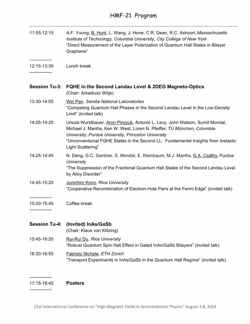
11:55-12:15 A.F. Young, B. Hunt, L. Wang, J. Hone, C.R. Dean, R.C. Ashoori, Massachusetts Institute of Technology, Columbia University, City College of New York “Direct Measurement of the Layer Polarization of Quantum Hall States in Bilayer Graphene”
--------------- 12:15-13:30 Lunch break ---------------
Session Tu-3: FQHE in the Second Landau Level & 2DEG Magneto-Optics
(Chair: Arkadiusz Wójs)
13:30-14:05 Wei Pan, Sandia National Laboratories “Competing Quantum Hall Phases in the Second Landau Level in the Low-Density Limit” (invited talk)
14:05-14:25 Ursula Wurstbauer, Aron Pinczuk, Antonio L. Levy, John Watson, Sumit Mondal, Michael J. Manfra, Ken W. West, Loren N. Pfeiffer, TU München, Columbia University, Purdue University, Princeton University “Unconventional FQHE States in the Second LL: Fundamental Insights from Inelastic Light Scattering”
14:25-14:45 N. Deng, G.C. Gardner, S. Mondal, E. Kleinbaum, M.J. Manfra, G.A. Csáthy, Purdue University “The Suppression of the Fractional Quantum Hall States of the Second Landau Level by Alloy Disorder”
14:45-15:20 Junichiro Kono, Rice University “Cooperative Recombination of Electron-Hole Pairs at the Fermi Edge” (invited talk)
--------------- 15:20-15:45 Coffee break ---------------
Session Tu-4: (Invited) InAs/GaSb
(Chair: Klaus von Klitzing)
15:45-16:20 Rui-Rui Du, Rice University “Robust Quantum Spin Hall Effect in Gated InAs/GaSb Bilayers” (invited talk)
16:20-16:55 Fabrizio Nichele, ETH Zürich “Transport Experiments in InAs/GaSb in the Quantum Hall Regime” (invited talk)
--------------- 17:15-18:45 Posters ---------------
HMF-21 Program
21st International Conference on "High Magnetic Fields in Semiconductor Physics" August 3-‐8, 2014
Wednesday, August 6, 2014
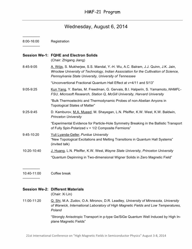
--------------- 8:00-16:00 Registration --------------- Session We-1: FQHE and Electron Solids
(Chair: Zhigang Jiang)
8:45-9:05 A. Wójs, S. Mukherjee, S.S. Mandal, Y.-H. Wu, A.C. Balram, J.J. Quinn, J.K. Jain, Wrocław University of Technology, Indian Association for the Cultivation of Science, Pennsylvania State University, University of Tennessee
“Unconvertional Fractional Quantum Hall Effect at v=4/11 and 5/13”
9:05-9:25 Kun Yang, Y. Barlas, M. Freedman, G. Gervais, B.I. Halperin, S. Yamamoto, NHMFL-FSU, Microsoft Research, Station Q, McGill University, Harvard University
“Bulk Thermoelectric and Thermodynamic Probes of non-Abelian Anyons in Topological States of Matter”
9:25-9:45 D. Kamburov, M.A. Mueed, M. Shayegan, L.N. Pfeiffer, K.W. West, K.W. Baldwin,
Princeton University
“Experimental Evidence for Particle-Hole Symmetry Breaking in the Ballistic Transport of Fully Spin-Polarized ν = 1/2 Composite Fermions”
9:45-10:20 Yuli Lyanda-Geller, Purdue University “New Topological Excitations and Melting Transitions in Quantum Hall Systems” (invited talk)
10:20-10:40 J. Huang, L.N. Pfeiffer, K.W. West, Wayne State University, Princeton University
“Quantum Depinning in Two-dimensional Wigner Solids in Zero Magnetic Field”
--------------- 10:40-11:00 Coffee break ---------------
Session We-2: Different Materials
(Chair: Xi Lin)
11:00-11:20 Q. Shi, M.A. Zudov, O.A. Mironov, D.R. Leadley, University of Minnesota, University of Warwick, International Laboratory of High Magnetic Fields and Low Temperatures, Poland
“Strongly Anisotropic Transport in p-type Ge/SiGe Quantum Well Induced by High In-plane Magnetic Fields”
HMF-21 Program
21st International Conference on "High Magnetic Fields in Semiconductor Physics" August 3-‐8, 2014
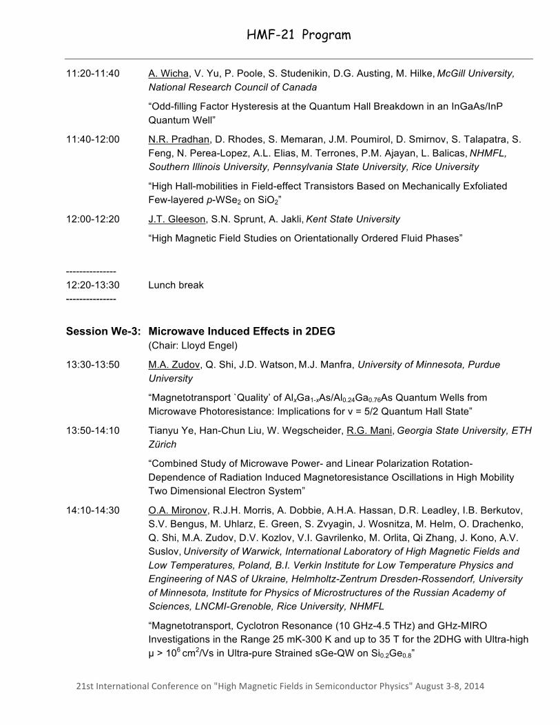
11:20-11:40 A. Wicha, V. Yu, P. Poole, S. Studenikin, D.G. Austing, M. Hilke, McGill University, National Research Council of Canada
“Odd-filling Factor Hysteresis at the Quantum Hall Breakdown in an InGaAs/InP Quantum Well”
11:40-12:00 N.R. Pradhan, D. Rhodes, S. Memaran, J.M. Poumirol, D. Smirnov, S. Talapatra, S. Feng, N. Perea-Lopez, A.L. Elias, M. Terrones, P.M. Ajayan, L. Balicas, NHMFL, Southern Illinois University, Pennsylvania State University, Rice University
“High Hall-mobilities in Field-effect Transistors Based on Mechanically Exfoliated Few-layered p-WSe2 on SiO2”
12:00-12:20 J.T. Gleeson, S.N. Sprunt, A. Jakli, Kent State University
“High Magnetic Field Studies on Orientationally Ordered Fluid Phases”
--------------- 12:20-13:30 Lunch break ---------------
Session We-3: Microwave Induced Effects in 2DEG
(Chair: Lloyd Engel)
13:30-13:50 M.A. Zudov, Q. Shi, J.D. Watson, M.J. Manfra, University of Minnesota, Purdue University
“Magnetotransport `Quality’ of AlxGa1-xAs/Al0.24Ga0.76As Quantum Wells from Microwave Photoresistance: Implications for ν = 5/2 Quantum Hall State”
13:50-14:10 Tianyu Ye, Han-Chun Liu, W. Wegscheider, R.G. Mani, Georgia State University, ETH Zürich
“Combined Study of Microwave Power- and Linear Polarization Rotation- Dependence of Radiation Induced Magnetoresistance Oscillations in High Mobility Two Dimensional Electron System”
14:10-14:30 O.A. Mironov, R.J.H. Morris, A. Dobbie, A.H.A. Hassan, D.R. Leadley, I.B. Berkutov, S.V. Bengus, M. Uhlarz, E. Green, S. Zvyagin, J. Wosnitza, M. Helm, O. Drachenko, Q. Shi, M.A. Zudov, D.V. Kozlov, V.I. Gavrilenko, M. Orlita, Qi Zhang, J. Kono, A.V. Suslov, University of Warwick, International Laboratory of High Magnetic Fields and Low Temperatures, Poland, B.I. Verkin Institute for Low Temperature Physics and Engineering of NAS of Ukraine, Helmholtz-Zentrum Dresden-Rossendorf, University of Minnesota, Institute for Physics of Microstructures of the Russian Academy of Sciences, LNCMI-Grenoble, Rice University, NHMFL
“Magnetotransport, Cyclotron Resonance (10 GHz-4.5 THz) and GHz-MIRO Investigations in the Range 25 mK-300 K and up to 35 T for the 2DHG with Ultra-high µ > 106 cm2/Vs in Ultra-pure Strained sGe-QW on Si0.2Ge0.8”
HMF-21 Program
21st International Conference on "High Magnetic Fields in Semiconductor Physics" August 3-‐8, 2014
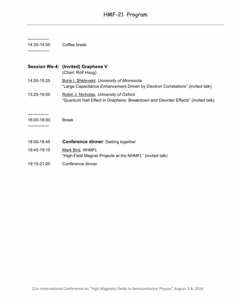
--------------- 14:30-14:50 Coffee break ---------------
Session We-4: (Invited) Graphene V (Chair: Rolf Haug)
14:50-15:25 Boris I. Shklovskii, University of Minnesota “Large Capacitance Enhancement Driven by Electron Correlations” (invited talk)
15:25-16:00 Robin J. Nicholas, University of Oxford “Quantum Hall Effect in Graphene: Breakdown and Disorder Effects” (invited talk)
--------------- 16:00-18:00 Break ---------------
18:00-18:45 Conference dinner: Getting together
18:45-19:15 Mark Bird, NHMFL “High-Field Magnet Projects at the NHMFL” (invited talk)
19:15-21:00 Conference dinner
HMF-21 Program
21st International Conference on "High Magnetic Fields in Semiconductor Physics" August 3-‐8, 2014
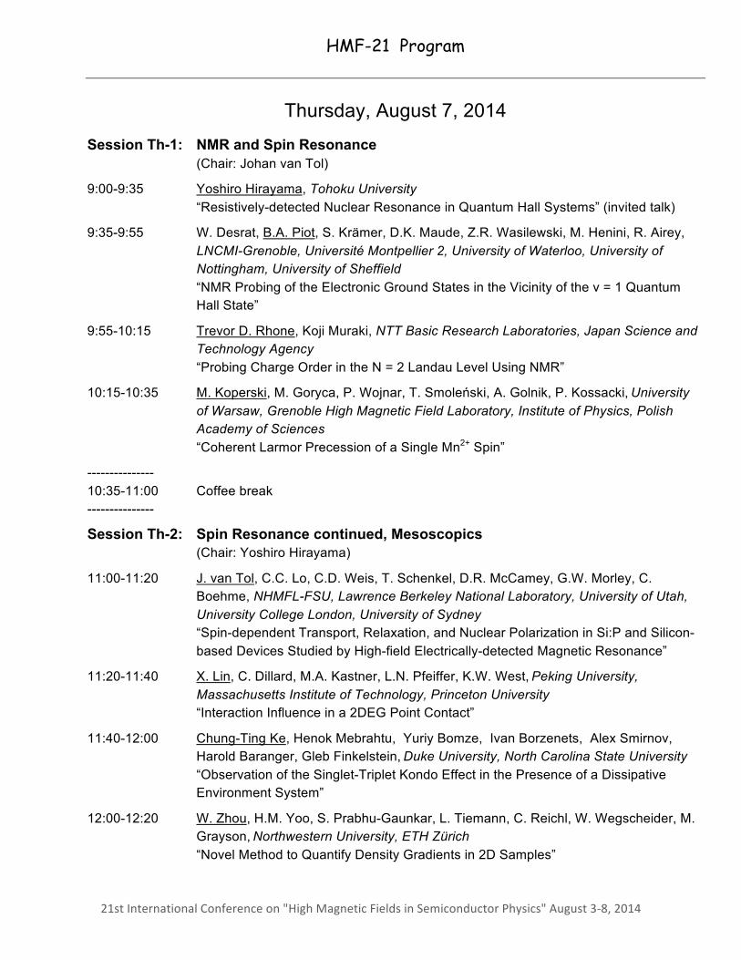
Thursday, August 7, 2014
Session Th-1: NMR and Spin Resonance (Chair: Johan van Tol)
9:00-9:35 Yoshiro Hirayama, Tohoku University “Resistively-detected Nuclear Resonance in Quantum Hall Systems” (invited talk)
9:35-9:55 W. Desrat, B.A. Piot, S. Krämer, D.K. Maude, Z.R. Wasilewski, M. Henini, R. Airey,
LNCMI-Grenoble, Université Montpellier 2, University of Waterloo, University of Nottingham, University of Sheffield “NMR Probing of the Electronic Ground States in the Vicinity of the ν = 1 Quantum Hall State”
9:55-10:15 Trevor D. Rhone, Koji Muraki, NTT Basic Research Laboratories, Japan Science and Technology Agency “Probing Charge Order in the N = 2 Landau Level Using NMR”
10:15-10:35 M. Koperski, M. Goryca, P. Wojnar, T. Smoleński, A. Golnik, P. Kossacki, University of Warsaw, Grenoble High Magnetic Field Laboratory, Institute of Physics, Polish Academy of Sciences “Coherent Larmor Precession of a Single Mn2+ Spin”
--------------- 10:35-11:00 Coffee break ---------------
Session Th-2: Spin Resonance continued, Mesoscopics (Chair: Yoshiro Hirayama)
11:00-11:20 J. van Tol, C.C. Lo, C.D. Weis, T. Schenkel, D.R. McCamey, G.W. Morley, C. Boehme, NHMFL-FSU, Lawrence Berkeley National Laboratory, University of Utah, University College London, University of Sydney “Spin-dependent Transport, Relaxation, and Nuclear Polarization in Si:P and Silicon-based Devices Studied by High-field Electrically-detected Magnetic Resonance”
11:20-11:40 X. Lin, C. Dillard, M.A. Kastner, L.N. Pfeiffer, K.W. West, Peking University, Massachusetts Institute of Technology, Princeton University “Interaction Influence in a 2DEG Point Contact”
11:40-12:00 Chung-Ting Ke, Henok Mebrahtu, Yuriy Bomze, Ivan Borzenets, Alex Smirnov, Harold Baranger, Gleb Finkelstein, Duke University, North Carolina State University “Observation of the Singlet-Triplet Kondo Effect in the Presence of a Dissipative Environment System”
12:00-12:20 W. Zhou, H.M. Yoo, S. Prabhu-Gaunkar, L. Tiemann, C. Reichl, W. Wegscheider, M. Grayson, Northwestern University, ETH Zürich “Novel Method to Quantify Density Gradients in 2D Samples”
HMF-21 Program
21st International Conference on "High Magnetic Fields in Semiconductor Physics" August 3-‐8, 2014
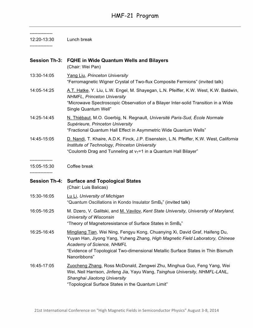
--------------- 12:20-13:30 Lunch break ---------------
Session Th-3: FQHE in Wide Quantum Wells and Bilayers
(Chair: Wei Pan)
13:30-14:05 Yang Liu, Princeton University “Ferromagnetic Wigner Crystal of Two-flux Composite Fermions” (invited talk)
14:05-14:25 A.T. Hatke, Y. Liu, L.W. Engel, M. Shayegan, L.N. Pfeiffer, K.W. West, K.W. Baldwin,
NHMFL, Princeton University “Microwave Spectroscopic Observation of a Bilayer Inter-solid Transition in a Wide Single Quantum Well”
14:25-14:45 N. Thiébaut, M.O. Goerbig, N. Regnault, Université Paris-Sud, École Normale Supérieure, Princeton University “Fractional Quantum Hall Effect in Asymmetric Wide Quantum Wells”
14:45-15:05 D. Nandi, T. Khaire, A.D.K. Finck, J.P. Eisenstein, L.N. Pfeiffer, K.W. West, California Institute of Technology, Princeton University “Coulomb Drag and Tunneling at νT=1 in a Quantum Hall Bilayer”
--------------- 15:05-15:30 Coffee break ---------------
Session Th-4: Surface and Topological States (Chair: Luis Balicas)
15:30-16:05 Lu Li, University of Michigan “Quantum Oscillations in Kondo Insulator SmB6” (invited talk)
16:05-16:25 M. Dzero, V. Galitski, and M. Vavilov, Kent State University, University of Maryland, University of Wisconsin “Theory of Magnetoresistance of Surface States in SmB6”
16:25-16:45 Mingliang Tian, Wei Ning, Fengyu Kong, Chuanying Xi, David Graf, Haifeng Du, Yuyan Han, Jiyong Yang, Yuheng Zhang, High Magnetic Field Laboratory, Chinese Academy of Science, NHMFL “Evidence of Topological Two-dimensional Metallic Surface States in Thin Bismuth Nanoribbons”
16:45-17:05 Zuocheng Zhang, Ross McDonald, Zengwei Zhu, Minghua Guo, Feng Yang, Wei Wei, Neil Harrison, Jinfeng Jia, Yayu Wang, Tsinghua University, NHMFL-LANL, Shanghai Jiaotong University “Topological Surface States in the Quantum Limit”
HMF-21 Program
21st International Conference on "High Magnetic Fields in Semiconductor Physics" August 3-‐8, 2014
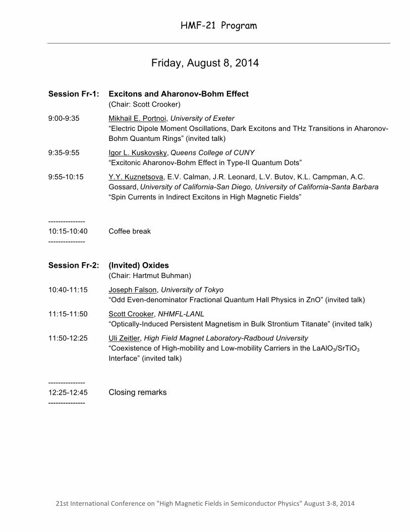
Friday, August 8, 2014
Session Fr-1: Excitons and Aharonov-Bohm Effect (Chair: Scott Crooker)
9:00-9:35 Mikhail E. Portnoi, University of Exeter “Electric Dipole Moment Oscillations, Dark Excitons and THz Transitions in Aharonov-Bohm Quantum Rings” (invited talk)
9:35-9:55 Igor L. Kuskovsky, Queens College of CUNY “Excitonic Aharonov-Bohm Effect in Type-II Quantum Dots”
9:55-10:15 Y.Y. Kuznetsova, E.V. Calman, J.R. Leonard, L.V. Butov, K.L. Campman, A.C. Gossard, University of California-San Diego, University of California-Santa Barbara “Spin Currents in Indirect Excitons in High Magnetic Fields”
--------------- 10:15-10:40 Coffee break ---------------
Session Fr-2: (Invited) Oxides
(Chair: Hartmut Buhman)
10:40-11:15 Joseph Falson, University of Tokyo “Odd Even-denominator Fractional Quantum Hall Physics in ZnO” (invited talk)
11:15-11:50 Scott Crooker, NHMFL-LANL “Optically-Induced Persistent Magnetism in Bulk Strontium Titanate” (invited talk)
11:50-12:25 Uli Zeitler, High Field Magnet Laboratory-Radboud University “Coexistence of High-mobility and Low-mobility Carriers in the LaAlO3/SrTiO3 Interface” (invited talk)
--------------- 12:25-12:45 Closing remarks ---------------

21st International Conference on "High Magnetic Fields in Semiconductor Physics" August 3-‐8, 2014
HMF-21
Invited and Contributed Talks

Mo-‐1-‐1 9:00-‐9:35 HMF-‐21 Mon 8/4
21st International Conference on "High Magnetic Fields in Semiconductor Physics" August 3-‐8, 2014
Correlated Electrons in Bilayer Graphene
Philip Kim
Harvard University, Cambridge, MA, USA
Spontaneous symmetry breaking occurring in an interacting many body system is one of the cornerstones of modern physics. Coulomb interaction has long been predicted to drive spontaneous breaking of the symmetry in the internal degrees of freedom of many electron systems, leading to exotic correlated electronic states. In graphene, the honeycomb arrangement of carbon atoms provides an extra degree of freedom to the quantum wave function of electrons in addition to electron spin. This new degree freedom is often termed as (valley) pseudo spin. Resulting four component internal degree of freedom (two spin and two valleys) is often refer to the SU(4) symmetry. In graphene, the strong Coulomb interactions and approximate spin-pseudo spin symmetry are predicted to lead to a variety of integer quantum Hall ferromagnetic (IQHF) and fractional quantum Hall (FQH) states and the quantum phase transition between them.
In particular, bilayer graphene provides a rich material platform for studying electronic interactions, hosting a variety of interacting ground states for the IQHEF and FQHE. Moreover we demonstrate the capability to tune phase transitions between different ground state orderings within the IQHF and FQHE states by application of a transverse electric field. To enable this, we have made innovations in graphene device preparation yielding samples of unprecedented quality, and explored correlated electronic states in these phase spaces in the quantum limit. We will discuss various phase transitions that can be tuned by a transverse electric field and magnetic fields. This result provides a model platform to study the role of symmetry breaking in emergent states with distinct topological order.

Mo-‐1-‐2 9:35-‐10:10 HMF-‐21 Mon 8/4
21st International Conference on "High Magnetic Fields in Semiconductor Physics" August 3-‐8, 2014
Graphene Superlattices and Double Layer Structures
Leonid Ponomarenko
Lancaster University, Bailrigg, Lancaster, UK
Recent advances in the fabrication of heterostructures based on 2D atomic crystals have opened up several new directions in graphene research [1]. It has recently been realised that hexagonal boron nitride (hBN) can be used not only as a defect free and atomically flat substrate that dramatically improves mobility of graphene devices, but also as a material that creates a smooth periodic potential for Dirac electrons in graphene. This potential arises due to the small lattice mismatch between the two materials resulting in the formation of a moiré pattern, as previously observed in STM measurements [2]. For aligned graphene and hBN crystals, the period of the superlattice potential is as large as 14 nm and leads to a dramatic reconstruction of the bend structure with the formation of new Dirac points in the spectrum. In high magnetic fields up to 30 T we approach the regime of one flux quanta per superlattice unit cell where the transport and capacitance data clearly reveal features of the spectrum predicted in the seminal paper of Douglas Hofstadter [3] known as the Hofstadter butterfly. More complex heterostructures in which two graphene sheets are separated by a thin layer of hBN are highly suitable for studying strongly interacting gases of Dirac fermions. The separation can be made as small as 1 nm (only 3 atomic layers of hBN), which is over a factor of 10 smaller than in the most advanced GaAs/AlGaAs double quantum well systems. Despite a small separation, the two graphene layers remain electrically isolated due to the wide band gap and high crystalline quality of hBN. To study such structures we employ Coulomb drag and quantum capacitance measurements. The former directly depends on the interlayer electron-electron scattering rate, while the latter is directly proportional to the density of states and may be used to probe many-body phenomena. In this presentation I will overview our recent results on the Hofstadter butterfly in graphene superlattices and experimental efforts in searching for interlayer excitons in double layer devices. References [1] A. K. Geim and I.V.Grigorieva. Nature 499, 419 (2013) [2] M. Yankowitz et al., Nature Physics 8, 382 (2012) [3] D. R. Hofstadter, Phys. Rev. B 14, 2239 (1976)

Mo-‐1-‐3 10:10-‐10:30 HMF-‐21 Mon 8/4
21st International Conference on "High Magnetic Fields in Semiconductor Physics" August 3-‐8, 2014
Preservation of Topological Berry Phase in Hydrogenated Graphene
T. Szkopek (1), K. Bennaceur (1), J. Guillemette (1), P.L. Lévesque (2), N. Cottenye (2), F. Mahvash (1,3), C. Proust (4), M. Siaj (3), R. Martel (2), G. Gervais (1)
1McGill University, Montréal, Canada
2Université de Montréal, Montréal, Canada 3Laboratoire National des Champs Magnétiques Intenses, CNRS, Toulouse, France
4Université du Québec à Montréal, Montréal, Canada
We report here magneto transport measurements at magnetic fields up to 55 T, including Shubnikov de Haas (SdH) and quantum Hall effect (QHE), of macroscopic hydrogenated graphene monolayers demonstrating experimentally that the topological Berry phase remains β=π in the presence of sub-lattice symmetry breaking. Hydrogenated graphene samples were prepared from monolayer graphene grown by chemical vapor deposition (CVD). Hydrogenation was performed in a UHV chamber with a thermally cracked atomic hydrogen source. The introduction of point defects by hydrogenation was confirmed by Raman spectroscopy. All samples, pristine and hydrogenated, displayed insulating behaviour, dR/dT<0. The highly resistive hydrogenated samples are well beyond the Ioffe-Regel limit for metallic conduction, yet are still capable of supporting a υ=-2 QHE state at high magnetic field [1]. Representative magneto transport measurements are shown in Fig. 1. The observed SdH oscillations were analyzed through a LL fan diagram, where the LL index and corresponding magnetic field 1/B are plotted in Fig. 1 for a representative sample HG78. The intercept at 1/B = 0 corresponds to the Berry phase shift β/2π = -0.47±0.16, consistent with β=±π. We thus conclude that the topological part of Berry phase, or equivalently the pseudo-spin winding number, is preserved despite the breaking of local sub-lattice
symmetry and strongly insulating zero field transport well beyond the Ioffe-Regel limit of conduction. Our observations provide the first experimental support for the theoretical prediction that the Berry phase in graphene is robust against sub-lattice symmetry breaking [2]. These observations are promising for the potential application of the topological properties of charge carriers to a host of electronic devices. This work was funded by the NSERC, CIFAR, FRQNT and the CRC program. A portion of this work was performed at the National High Magnetic Field Laboratory which is supported by NSF Cooperative Agreement No. DMR-0084173, the State of Florida, and the DOE, and the Laboratoire National de Champs Magnétiques Intenses (LNCMI) located in Toulouse, France. References [1] J. Guillemette et al., Phys. Rev. Lett., 110, 176801 (2013). [2] J.N. Fuchs et al., Eur. Phys. J. B, 77, 351 (2010).
(b)
1/B [ 1/T ]0.060.040.02 0.08 0.10
LL in
dex,
N
-2
-4
-6HG 78 VG=-90 V
VG=15 V
1/BF
-3
-5
-1
0.00
ћ2�
= -0.47±0.16
20 -75B [ T ] 0
(a)
R2p
t [ h
/e2
]
4060
10
-3015
V G [ V ]
1
10
1
Fig. 1: (a) Measured 2-point resistance of a hydrogenated graphene sample versus magnetic field B and gate voltage VG. (b) Landau fan diagram showing extraction of SdH frequency BF and Berry phase β.
Mo-‐2-‐1 11:00-‐11:35 HMF-‐21 Mon 8/4
21st International Conference on "High Magnetic Fields in Semiconductor Physics" August 3-‐8, 2014
Magnetic Field Induced Localized Majorana Modes in Semiconductors
Sankar Das Sarma
University of Maryland, College Park, MD, USA
Mo-‐2-‐2 11:35-‐12:10 HMF-‐21 Mon 8/4
21st International Conference on "High Magnetic Fields in Semiconductor Physics" August 3-‐8, 2014
Surface-state Transport in a 3D Topological Insulator
Hartmut Buhmann
Physikalisches Institut, Universität Würzburg, Am Hubland, 97074 Würzburg, Germany Topological insulators (TI) are characterized by an insulating bulk and conducting surfaces. The conducting surface states exhibit a characteristic Dirac band dispersion and therefore offer a lot of new and interesting properties, especially with respect to future device applications. In this presentation, the material system of mercury-telluride (HgTe) is introduced as a proto-type for the investigation of topological transport properties in two-dimensional (2D) as well as in three-dimensional (3D) systems. The realization of a 2D TI structure in HgTe quantum wells has already demonstrated the potential for spin injection and detection purposes in spintronics applications without any magnetic materials or applied magnetic fields [1,2,3]. However, transport experiments on 3D TI surface states are rare, even though numerous TI materials have been identified and fabricated worldwide. Here, the magneto-transport characterization data of strained HgTe bulk layers are presented which show characteristic Dirac-like quantum Hall-effect sequences. The quantum Hall features originate from those two 2D TI surfaces which are oriented perpendicular to the applied magnetic field [4]. Using top and back-gated sample structures it is possible to distinguish their specific contributions. Surprisingly, unobscured clear surface transport is observable over a wide density range, covering the n- and p-conducting regime, extended into a regime where usually bulk transport is expected to dominate. The latter points to the extraordinary properties of Dirac surface states. Furthermore, we were able to demonstrate the feasibility of proximity induced superconductivity in the surface of a 3D TI [5,6].
References [1] M. König et al., Science 318, 766 (2007). [2] A. Roth et al., Science 325, 294 (2009). [3] C. Brüne et al., Nature Physics 8, 485 (2012). [4] C. Brüne et al., Phys. Rev. Lett. 106, 126803 (2011). [5] L. Maier et al., Phys. Rev. Lett. 109, 186806 (2012). [6] J.B. Oostinga et al., Phys. Rev. X 3, 021007 (2013).

Mo-‐3-‐1 13:30-‐14:05 HMF-‐21 Mon 8/4
21st International Conference on "High Magnetic Fields in Semiconductor Physics" August 3-‐8, 2014
Andreev Spectroscopy in the Quantum Hall Regime in Bilayer Graphene
Dmitri K. Efetov1, Clevin Handschin1, Lei Wang2, James Hone2, Cory Dean3 and Philip Kim1
1Columbia University, Department of Physics 2Columbia University, Department of Mechanical Engineering
3CCNY, Department of Physics
Inducing Superconductivity (SC) via proximity effect into the topological edge states of a 2-dimensional (2D) conductor in the Quantum Hall Regime (QHE) has been a long standing proposition which has recently reinvigorated attention. Such devices would allow to study the proximity effect in the ballistic 2D limit, where predictions go as far as specular Andreev Reflections in single layer graphene, the formation of Andreev Bound States along the SN interface in strong magnetic fields and Andreev Edge States in the Quantum Hall Regime and go as far as the possible formation of Majorana zero modes. Here we present a new route for fabricating such devices made entirely out of cleanly stacked layered van der Waals materials BN/Graphene/NbSe2. The formidable electric contact between the type-II superconductor NbSe2 and the high mobility BN/graphene Hallbar allows to perform Andreev Reflection spectroscopy of the fully developed Quantum Hall states. Here, we observe a clear enhancement of the Andreev Reflection probability when Cooper Pairs are injected into the incompressible Quantum Hall states. This finding can be explained as the result of Andreev Bound States formation at the SN interface and can be also linked to the chiral nature of the topological edge states and the absence of back-scattering. We furthermore tie these finding with the observation of renormalized values of the Quantum Hall plateaus below the upper critical field of NbSe2 of Hc2 = 4T.
Fig. 1. a) +b) Optical image of the device and transfer assembly process. c) R vs. T and R vs. B of NbSe2 with Tc ~ 7.2K and Hc2 ~ 4T. d.) Rxx and Rxy vs. Vbg showing fully developed QHE at B ~ 1T. Fig. 2. Colorplot of the normalized conductance as a function voltage across the SN interface, showing co-existence of the QHE and Andreev Reflections up to B=4T and its systematic change when injected into compressible vs. incompressible QH states.
Mo-‐3-‐2 14:05-‐14:25 HMF-‐21 Mon 8/4
21st International Conference on "High Magnetic Fields in Semiconductor Physics" August 3-‐8, 2014
Theory of the Electronic Properties of Triangular Graphene Quantum Dots in a Magnetic Field
P. Potasz (1), A.D. Guclu(2), P. Hawrylak (3)
1Institute of Physics, Wroclaw University of Technology, Wroclaw, Poland
2Department of Physics, Izmir Institute of Technology, Izmir, Turkey 3Quantum Theory Group, Security and Disruptive Technology, Emerging Technologies Division, National Research
Council of Canada, Ottawa, Canada and Department of Physics, University of Ottawa, Ottawa, Canada
We present new results describing the electronic properties of triangular graphene quantum dots with zigzag edges (TGQDs) in a magnetic field [1- 3]. TGQDs are of particular interest due to a broken sublattice symmetry resulting in a presence of a degenerate electronic shell at the Fermi level, in the middle of a size dependent energy gap [4-10]. Using the tight-binding model in the nearest neighbor approximation with the magnetic field included by Peierls substitution [11], we derive a semi-analytical form of eigenvectors corresponding to states of degenerate shell [12]. We show that the energy of the degenerate shell is immune to the applied magnetic field in analogy with states of the zero-th Landau level (0LL) of bulk graphene. Due to formation of 0LL in TGQDs, the energy gap is shown to close with increasing magnetic field, reaching zero at special values of the magnetic field. We extend the one electron calculations to include electron-electron interactions within both mean-field models, and beyond, using a combination of tight-binding, Hartree-Fock and configuration interaction methods (tb-HF-CI) [7-10]. We analyze interactions between spin polarized electrons of the degenerate spin polarized electronic shell and electrons distributed on the 0LL states as a function of the number of electron-hole pairs, spin flips and increasing magnetic field. A possibility of an occurrence of excitonic instability is discussed [13]. References [1] M. Zarenia, A. Chaves, G. A. Farias, and F. M. Peeters, Phys. Rev. B 84, 245403 (2011). [2] D. A. Bahamon, A. L. C. Pereira, and P. A. Schulz, Phys. Rev. B 79, 125414 (2009). [3] I. Romanovsky, C. Yannouleas, and U. Landman, Phys. Rev. B 83, 045421 (2011). [4] M. Ezawa, Phys. Rev. B 76, 245415 (2007). [5] J. Fernandez-Rossier and J. J. Palacios, Phys. Rev. Lett. 99, 177204 (2007). [6] W. L. Wang, S. Meng, and E. Kaxiras, Nano Lett. 8, 241 (2008). [7] A. D. Güçlü et al., Phys. Rev. Lett. 103, 246805 (2009). [8] P. Potasz, A. D. Guclu, P. Hawrylak, Phys. Rev. B 81, 033403 (2010). [9] A. D. Güçlü, P. Potasz, and P. Hawrylak, Phys. Rev. B 82, 155445 (2010). [10] P. Potasz, A. D. Guclu, A. Wojs, P. Hawrylak, Phys. Rev. B 85, 075431 (2012). [11] R. E. Peierls, Z. Phys. 80, 763 (1933). [12] A. D. Güçlü, P. Potasz, and P. Hawrylak, Phys. Rev. B 88, 155429 (2013). [13] Tomi Paananen and Reinhold Egger, Phys. Rev. B 84, 155456 (2011).

Mo-‐3-‐3 14:25-‐14:45 HMF-‐21 Mon 8/4
21st International Conference on "High Magnetic Fields in Semiconductor Physics" August 3-‐8, 2014
Giant Interaction-induced Gap and Electronic Phases in Rhombohedral Trilayer Graphene
Y. Lee (1), D. Tran (1), K. Myhro (1), J. Velasco Jr. (1), K. Myhro (1), N. Gillgren (1), Y. Barlas (1),
J.M. Poumirol (2) , D. Smirnov (2), F. Guinea (3) and C.N. Lau (1)
1Department of Physics and Astronomy, University of California, Riverside, USA 2National High Magnetic Field Laboratory, Tallahassee, USA
2ICMM-CSIC, Madrid, Spain
In rhombohedral-stacked trilayer graphene (r-TLG), the cubic dispersion and large density of states near the charge neutrality point give rise to large electronic interactions and a variety of possible symmetry-broken phases. Here, using transport measurements, we show that, contrary to predictions by tight-binding calculations, r-TLG is an intrinsic insulator, with a giant interaction-induced gap Δ~42meV. This insulating state is a spontaneous layer antiferromagnetic with broken time reversal symmetry, and can be suppressed by increasing charge density n, an interlayer potential U, a parallel magnetic field, or a critical temperature Tc~38K.
References [1] Y. Lee, D. Tran. K. Myhro, J. Velasco Jr,. N. Gillgren, Y. Barlas, J.M. Poumirol, D. Smirnov, F.Guinea and C.N. Lau arXiv; 1402.6413v1(2014).
Fig. 1. a. G(n) at =0. Note the logarithmic scale of G. Inset: Energy-momentum dispersion of r-TLG. b. G( , n) in units of e2/h. c. G(V) at =n=0. Inset: SEM image of a dual-gated TLG device.
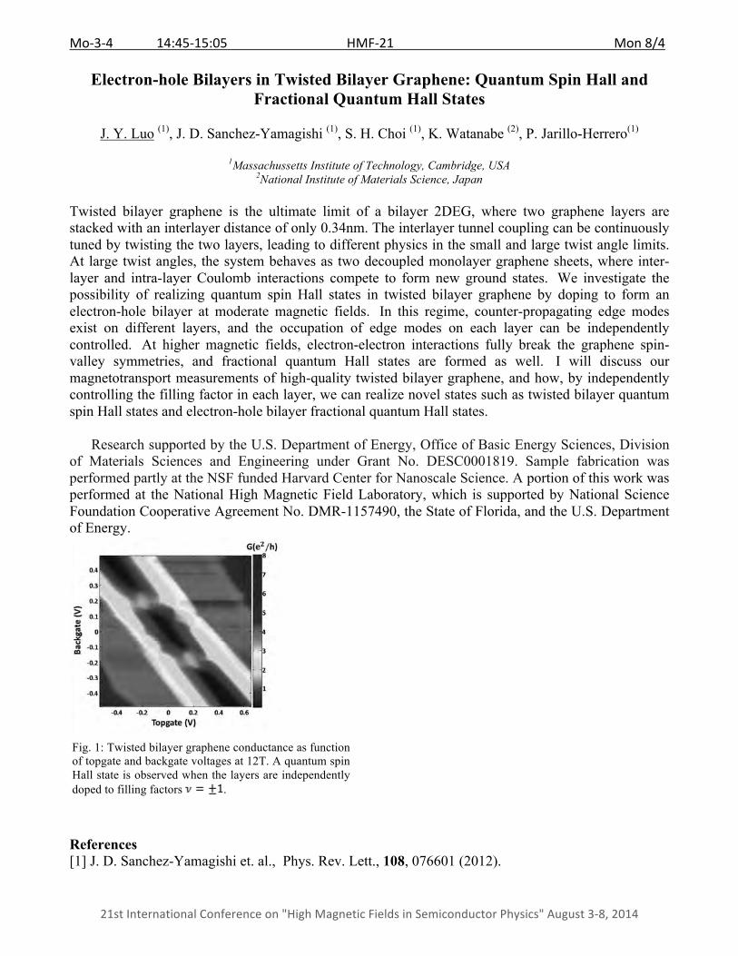
Mo-‐3-‐4 14:45-‐15:05 HMF-‐21 Mon 8/4
21st International Conference on "High Magnetic Fields in Semiconductor Physics" August 3-‐8, 2014
Electron-hole Bilayers in Twisted Bilayer Graphene: Quantum Spin Hall and Fractional Quantum Hall States
J. Y. Luo (1), J. D. Sanchez-Yamagishi (1), S. H. Choi (1), K. Watanabe (2), P. Jarillo-Herrero(1)
1Massachussetts Institute of Technology, Cambridge, USA
2National Institute of Materials Science, Japan
Twisted bilayer graphene is the ultimate limit of a bilayer 2DEG, where two graphene layers are stacked with an interlayer distance of only 0.34nm. The interlayer tunnel coupling can be continuously tuned by twisting the two layers, leading to different physics in the small and large twist angle limits. At large twist angles, the system behaves as two decoupled monolayer graphene sheets, where inter-layer and intra-layer Coulomb interactions compete to form new ground states. We investigate the possibility of realizing quantum spin Hall states in twisted bilayer graphene by doping to form an electron-hole bilayer at moderate magnetic fields. In this regime, counter-propagating edge modes exist on different layers, and the occupation of edge modes on each layer can be independently controlled. At higher magnetic fields, electron-electron interactions fully break the graphene spin-valley symmetries, and fractional quantum Hall states are formed as well. I will discuss our magnetotransport measurements of high-quality twisted bilayer graphene, and how, by independently controlling the filling factor in each layer, we can realize novel states such as twisted bilayer quantum spin Hall states and electron-hole bilayer fractional quantum Hall states.
Research supported by the U.S. Department of Energy, Office of Basic Energy Sciences, Division of Materials Sciences and Engineering under Grant No. DESC0001819. Sample fabrication was performed partly at the NSF funded Harvard Center for Nanoscale Science. A portion of this work was performed at the National High Magnetic Field Laboratory, which is supported by National Science Foundation Cooperative Agreement No. DMR-1157490, the State of Florida, and the U.S. Department of Energy.
References [1] J. D. Sanchez-Yamagishi et. al., Phys. Rev. Lett., 108, 076601 (2012).
Fig. 1: Twisted bilayer graphene conductance as function of topgate and backgate voltages at 12T. A quantum spin Hall state is observed when the layers are independently doped to filling factors .
Mo-‐4-‐1 15:30-‐16:05 HMF-‐21 Mon 8/4
21st International Conference on "High Magnetic Fields in Semiconductor Physics" August 3-‐8, 2014
Massless Fermions in 2D and 3D: Infrared Magneto-spectroscopy Studies
Milan Orlita
Laboratoire National des Champs Magnétiques Intenses, CNRS-UJF-UPS-INSA, 38042 Grenoble, France
Solid-state physics and quantum electrodynamics, with its relativistic (massless) particles, meet to their mutual benefit in steadily expanding class of materials. Those include, 1D carbon nanotubes, 2D graphene or topological-insulator surfaces, and, most recently, the systems with an isotropic conical dispersion in 3D - with Weyl, Dirac or Kane fermions. In this talk, I will review how the linear dispersion impacts the basic (magneto-) optical properties of these systems.
To illustrate this, we focus on two representative materials: a 2D graphene [1] and bulk HgCdTe [2] which displays the 3D conical dispersion when tuned to the point of the semiconductor-to-semimetal topological transition. We demonstrate that it is the number of dimensions, which defines the (joint) density of states, and in consequence, the simple physical quantities such as absorption of light - dispersionless in graphene but displaying a linear-in-photon-energy dependence in HgCdTe. In magnetic fields, the conical dispersion is transformed into Landau levels (LLs) and the optical response is determined by electronic excitations between discrete (in 2D) or dispersed (in 3D) LLs, both, however, with a typical for relativistic particles, square root dependence on the magnetic-field. Further relativistic effects may appear, depending on the strength of spin-orbit coupling. Spin-related effects are rather absent in the optical response of graphene which exhibits a weak spin-orbit coupling. Instead, we observe a pronounced spin splitting of LLs in HgCdTe, which follows the √B-dependence - a well-established signature of relativistic particles, but never observed in any condensed-matter system up to now. References [1] M. Orlita and M. Potemski, Semicond. Sci. Technol. 25, 063001 (2010). [2] M. Orlita et al., Nature Physics 10, 233 (2014).
Mo-‐4-‐2 16:05-‐16:25 HMF-‐21 Mon 8/4
21st International Conference on "High Magnetic Fields in Semiconductor Physics" August 3-‐8, 2014
THz Photovoltaic Effects in HgTe 2DEGs in the Region of Cyclotron Resonance
M. Pakmehr (1), C. Brüne (2), L. Molenkamp (2), B. D. McCombe (1)
1Department of Physics, University at Buffalo, SUNY, Buffalo, NY 14260, U.S.A 2EP3, University of Wuerzburg, D-97074 Wuertzburg, Germany
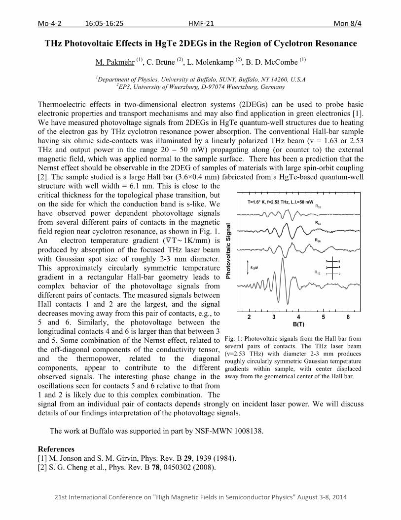
Thermoelectric effects in two-dimensional electron systems (2DEGs) can be used to probe basic electronic properties and transport mechanisms and may also find application in green electronics [1]. We have measured photovoltage signals from 2DEGs in HgTe quantum-well structures due to heating of the electron gas by THz cyclotron resonance power absorption. The conventional Hall-bar sample having six ohmic side-contacts was illuminated by a linearly polarized THz beam (v = 1.63 or 2.53 THz and output power in the range 20 – 50 mW) propagating along (or counter to) the external magnetic field, which was applied normal to the sample surface. There has been a prediction that the Nernst effect should be observable in the 2DEG of samples of materials with large spin-orbit coupling [2]. The sample studied is a large Hall bar (3.6×0.4 mm) fabricated from a HgTe-based quantum-well structure with well width = 6.1 nm. This is close to the critical thickness for the topological phase transition, but on the side for which the conduction band is s-like. We have observed power dependent photovoltage signals from several different pairs of contacts in the magnetic field region near cyclotron resonance, as shown in Fig. 1. An electron temperature gradient ( T 1K/mm) is produced by absorption of the focused THz laser beam with Gaussian spot size of roughly 2-3 mm diameter. This approximately circularly symmetric temperature gradient in a rectangular Hall-bar geometry leads to complex behavior of the photovoltage signals from different pairs of contacts. The measured signals between Hall contacts 1 and 2 are the largest, and the signal decreases moving away from this pair of contacts, e.g., to 5 and 6. Similarly, the photovoltage between the longitudinal contacts 4 and 6 is larger than that between 3 and 5. Some combination of the Nernst effect, related to the off-diagonal components of the conductivity tensor, and the thermopower, related to the diagonal components, appear to contribute to the different observed signals. The interesting phase change in the oscillations seen for contacts 5 and 6 relative to that from 1 and 2 is likely due to this complex combination. The signal from an individual pair of contacts depends strongly on incident laser power. We will discuss details of our findings interpretation of the photovoltage signals. The work at Buffalo was supported in part by NSF-MWN 1008138. References [1] M. Jonson and S. M. Girvin, Phys. Rev. B 29, 1939 (1984). [2] S. G. Cheng et al., Phys. Rev. B 78, 0450302 (2008).
Fig. 1: Photovoltaic signals from the Hall bar from several pairs of contacts. The THz laser beam (v=2.53 THz) with diameter 2-3 mm produces roughly circularly symmetric Gaussian temperature gradients within sample, with center displaced away from the geometrical center of the Hall bar.

Mo-‐4-‐3 16:25-‐16:45 HMF-‐21 Mon 8/4
21st International Conference on "High Magnetic Fields in Semiconductor Physics" August 3-‐8, 2014
Quantized Transport in HgTe-based p-2D Semimetal-p Junction
G.M. Gusev(1), E.B. Olshanetsky(2), Z.D. Kvon(2,3), A.D. Levin(1), Y. Krupko(4), J.C. Portal(4,5), N.N. Mikhailov(2), and S.A. Dvoretsky(2)
1Instituto de Física da Universidade de São Paulo, 135960-170, São Paulo, SP, Brazil
2Institute of Semiconductor Physics, Novosibirsk 630090, Russia 3Novosibirsk State University, Novosibirsk, 630090, Russia
4LNCMI-CNRS, UPR 3228, BP 166, 38042 Grenoble Cedex 9, France 8 5INSA Toulouse, 31077 Toulouse Cedex 4, France
Recently it has been demonstrated that the density variation across the charge neutrality point in n-p-n
graphene junctions results to the fractional resistance quantization in the presence of the perpendicular magnetic field [1]. The character of the Quantum Hall effect (QHE) transport in unipolar and bipolar regimes is quite different. In the unipolar regime the edge states propagate in the same direction, while in the bipolar regime the edge states counter-circulate in the p and n regions, propagating parallel to each other along the interface. The intermode scattering across the interface in the presence of the disorder leads to interference between channels, and conductance should exhibit fractional quantization. In the present paper, we report the realization of local top gating in a HgTe- based 20 nm quantum well for which the density in each region could be varied across the gap, allowing a p-n-p junction to be formed at the interfaces. The strained 20 nm HgTe QW is a semimetal with a zero gap so it does not have the quantum spin Hall effect in contrast to 8 nm HgTe samples. When the Fermi energy in the region under the local gate lies in the bulk gap band, the transport at the junction interface is described by mode mixing between conventional QHE edge channels and pairs of counter-propagating modes with opposite spin polarizations (figure1), corresponding to charge neutrality point (n=p) in semimetal. We find the fractional quantum Hall effect plateaux R =2h/e2 in the p-p`-p regime in accordance with a mode
describing the counter-circulate mixing edge state model. In p-n-p region we observed reproducible mesoscopic conductance fluctuations, demonstrating that our samples are sufficiently small and transport would be expected to be coherent. References [1] B. Özyilmaz, P. Jarillo-Herrero, D. Efetov, D. A. Abanin, L. S. Levitov, and P. Kim, Phys. Rev. Lett. 99, 166804, (2007).
Fig. 1: Schematics of edge state propagation for different charge densities in the central local gate region (red rectangular) and in the regions outside the local gate in the strong magnetic field. Right-the energy spectrum.
Fig. 2: The longitudinal resistance as a function of the gate voltage and magnetic field. .
Tu-‐1-‐1 9:00-‐9:35 HMF-‐21 Tue 8/5
21st International Conference on "High Magnetic Fields in Semiconductor Physics" August 3-‐8, 2014
Ballistic Transport in Epitaxial Graphene Nanoribbons
Walter A. de Heer
Georgia Institute of Technology, Atlanta, GA, USA
Graphene nanoribbons are essential components in future graphene nanoelectronics. However, in typical nanoribbons produced from lithographically patterned exfoliated graphene, the charge carriers travel only about 10 nanometers between scattering events, resulting in minimum sheet resistances of about 1 kΩ. In contrast 40 nm wide graphene nanoribbons that are epitaxially grown on silicon carbide are single channel room temperature ballistic conductors on greater than 10 µm length scale, similarly to metallic carbon nanotubes. This is equivalent to sheet resistances below 1Ω, surpassing theoretical predictions for perfect graphene by at least an order of magnitude. In neutral graphene ribbons, we show that transport is dominated by two modes. One is ballistic and temperature independent; the other is thermally activated. Transport is protected from back-scattering, possibly reflecting ground state properties of neutral graphene. At room temperature the resistance of both modes abruptly increases non-linearly with increasing length, one at a length of 16 µm and the other at 160 nm. Besides their importance for fundamental science, since epitaxial graphene nanoribbons are readily produced by the thousands, their room temperature ballistic transport properties can be used in advanced nanoelectronics as well.
Tu-‐1-‐2 9:35-‐9:55 HMF-‐21 Tue 8/5
21st International Conference on "High Magnetic Fields in Semiconductor Physics" August 3-‐8, 2014
Electrical Switch to the Resonant Magneto-Phonon Effect in Graphene
P. Leszczynski1, Z. Han2, A.A.L. Nicolet1, B.A. Piot1, P. Kossacki3, M. Orlita1, V. Bouchiat3, D.M. Basko4, M. Potemski1, C. Faugeras1
1LNCMI (CNRS, UJF, UPS, INSA), BP 166, 38042 Grenoble Cedex 9, France
2Institut Néel, CNRS-UJF-INP, 38042 Grenoble Cedex 09, France 3Institute of Experimental Physics, University of Warsaw, Hoza 69, Warsaw 00-681, Poland
4Université Grenoble 1/CNRS, LPMMC UMR 5493, 25 rue des Martyrs, 38042 Grenoble, France
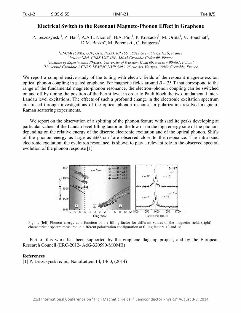
We report a comprehensive study of the tuning with electric fields of the resonant magneto-exciton optical phonon coupling in gated graphene. For magnetic fields around B 25 T that correspond to the range of the fundamental magneto-phonon resonance, the electron–phonon coupling can be switched on and off by tuning the position of the Fermi level in order to Pauli block the two fundamental inter-Landau level excitations. The effects of such a profound change in the electronic excitation spectrum are traced through investigations of the optical phonon response in polarization resolved magneto-Raman scattering experiments. We report on the observation of a splitting of the phonon feature with satellite peaks developing at particular values of the Landau level filling factor on the low or on the high energy side of the phonon, depending on the relative energy of the discrete electronic excitation and of the optical phonon. Shifts of the phonon energy as large as ±60 cm–1 are observed close to the resonance. The intra-band electronic excitation, the cyclotron resonance, is shown to play a relevant role in the observed spectral evolution of the phonon response [1].
Part of this work has been supported by the graphene flagship project, and by the European Research Council (ERC-2012- AdG-320590-MOMB) References [1] P. Leszczynski et al., NanoLetters 14, 1460, (2014)
Fig. 1: (left) Phonon energy as a function of the filling factor for different values of the magnetic field. (right) characteristic spectra measured in different polarization configuration at filling factors ±2 and ±6.
Tu-‐1-‐3 9:55-‐10:15 HMF-‐21 Tue 8/5
21st International Conference on "High Magnetic Fields in Semiconductor Physics" August 3-‐8, 2014
Observation of a Large Intrinsic Bandgap and Landau Level Renormalization in Graphene/Boron-nitride Heterostructures
Zhi-Guo Chen (1), Zhiwen Shi (2), Wei Yang (3), Xiaobo Lu (3), You Lai (1), Hugen Yan (4), Feng Wang
(2,5), Guangyu Zhang (3) and Zhiqiang Li (1)
1National High Magnetic Field Laboratory, Tallahassee, Florida 32310, USA 2Department of Physics, University of California at Berkeley, Berkeley, California 94720, USA
3Beijing National Laboratory for Condensed Matter Physics and Institute of Physics, Chinese Academy of Sciences, Beijing 100190, China
4IBM Thomas J. Watson Research Center, Yorktown Heights, New York 10598, USA 5Materials Science Division, Lawrence Berkeley National Laboratory, Berkeley, California 94720, USA
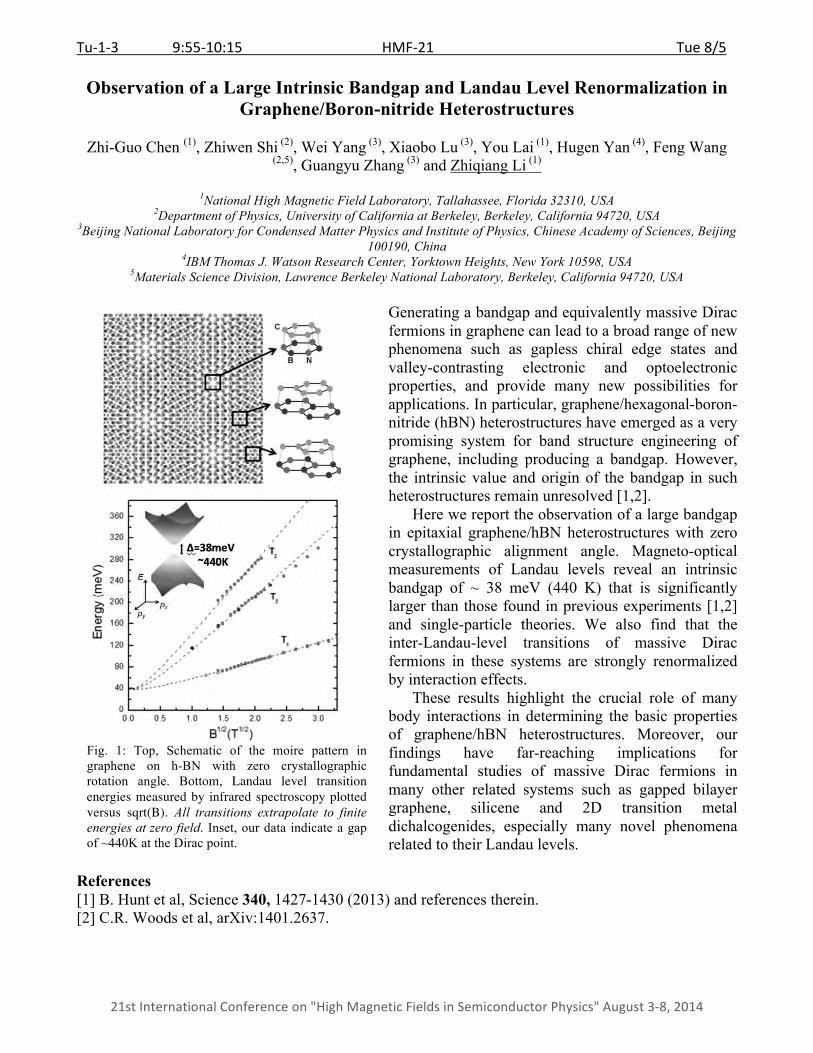
Generating a bandgap and equivalently massive Dirac fermions in graphene can lead to a broad range of new phenomena such as gapless chiral edge states and valley-contrasting electronic and optoelectronic properties, and provide many new possibilities for applications. In particular, graphene/hexagonal-boron-nitride (hBN) heterostructures have emerged as a very promising system for band structure engineering of graphene, including producing a bandgap. However, the intrinsic value and origin of the bandgap in such heterostructures remain unresolved [1,2]. Here we report the observation of a large bandgap in epitaxial graphene/hBN heterostructures with zero crystallographic alignment angle. Magneto-optical measurements of Landau levels reveal an intrinsic bandgap of ~ 38 meV (440 K) that is significantly larger than those found in previous experiments [1,2] and single-particle theories. We also find that the inter-Landau-level transitions of massive Dirac fermions in these systems are strongly renormalized by interaction effects. These results highlight the crucial role of many body interactions in determining the basic properties of graphene/hBN heterostructures. Moreover, our findings have far-reaching implications for fundamental studies of massive Dirac fermions in many other related systems such as gapped bilayer graphene, silicene and 2D transition metal dichalcogenides, especially many novel phenomena related to their Landau levels.
References [1] B. Hunt et al, Science 340, 1427-1430 (2013) and references therein. [2] C.R. Woods et al, arXiv:1401.2637.
Fig. 1: Top, Schematic of the moire pattern in graphene on h-BN with zero crystallographic rotation angle. Bottom, Landau level transition energies measured by infrared spectroscopy plotted versus sqrt(B). All transitions extrapolate to finite energies at zero field. Inset, our data indicate a gap of ~440K at the Dirac point.
Tu-‐1-‐4 10:15-‐10:35 HMF-‐21 Tue 8/5
21st International Conference on "High Magnetic Fields in Semiconductor Physics" August 3-‐8, 2014
Strong Auger Scattering in Landau-quantized Graphene Investigated by Infrared Pump-probe Experiments
M. Mittendorff(1,2), F. Wendler(3), E. Malic(3), A. Knorr(3), M. Orlita(4,5), M. Potemski(4), C. Berger(6,7),
W. A. de Heer(6), H. Schneider(1), M. Helm(1,2), and S. Winnerl(1)
1Helmholtz-Zentrum Dresden-Rossendorf, P.O. Box 510119, 01314 Dresden, Germany 2Technische Universität Dresden, 01062 Dresden, Germany
3Technische Universität Berlin, Hardenbergstraße 36, 10623 Berlin, Germany 4Grenoble High Magnetic Field Laboratory, CNRS-UJF-UPS-INSA, 38042 Grenoble, France
5Charles University Faculty of Mathematics and Physics, Ke Karlovu 5, 121 16 Praha, Czech Republic 6Georgia Institute of Technology, Georgia, Atlanta 30332, United States
7CNRS – Institut Néel, 38042 Grenoble, France
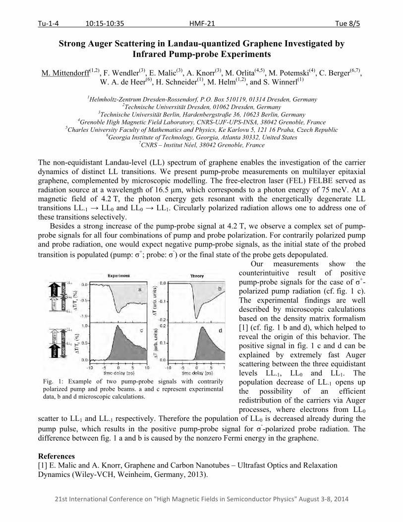
The non-equidistant Landau-level (LL) spectrum of graphene enables the investigation of the carrier dynamics of distinct LL transitions. We present pump-probe measurements on multilayer epitaxial graphene, complemented by microscopic modelling. The free-electron laser (FEL) FELBE served as radiation source at a wavelength of 16.5 µm, which corresponds to a photon energy of 75 meV. At a magnetic field of 4.2 T, the photon energy gets resonant with the energetically degenerate LL transitions LL-1 → LL0 and LL0 → LL1. Circularly polarized radiation allows one to address one of these transitions selectively. Besides a strong increase of the pump-probe signal at 4.2 T, we observe a complex set of pump-probe signals for all four combinations of pump and probe polarization. For contrarily polarized pump and probe radiation, one would expect negative pump-probe signals, as the initial state of the probed transition is populated (pump: σ+; probe: σ-) or the final state of the probe gets depopulated.
Our measurements show the counterintuitive result of positive pump-probe signals for the case of σ+-polarized pump radiation (cf. fig. 1 c). The experimental findings are well described by microscopic calculations based on the density matrix formalism [1] (cf. fig. 1 b and d), which helped to reveal the origin of this behavior. The positive signal in fig. 1 c and d can be explained by extremely fast Auger scattering between the three equidistant levels LL-1, LL0 and LL1. The population decrease of LL-1 opens up the possibility of an efficient redistribution of the carriers via Auger processes, where electrons from LL0
scatter to LL1 and LL-1 respectively. Therefore the population of LL0 is decreased already during the pump pulse, which results in the positive pump-probe signal for σ--polarized probe radiation. The difference between fig. 1 a and b is caused by the nonzero Fermi energy in the graphene.
References [1] E. Malic and A. Knorr, Graphene and Carbon Nanotubes – Ultrafast Optics and Relaxation Dynamics (Wiley-VCH, Weinheim, Germany, 2013).
Fig. 1: Example of two pump-probe signals with contrarily polarized pump and probe beams. a and c represent experimental data, b and d microscopic calculations.

Tu-‐2-‐1 11:00-‐11:35 HMF-‐21 Tue 8/5
21st International Conference on "High Magnetic Fields in Semiconductor Physics" August 3-‐8, 2014
Hofstadter’s Butterfly in the Clean Limit
Cory Dean
Columbia University, New York, NY, USA
In 1976, Douglas Hofstadter predicted that in the presence of both a strong magnetic field, and a spatially varying periodic potential, Bloch electrons confined to a 2D quantum well exhibit a self-similar fractal energy spectrum known as the "Hofstadter's Butterfly". In subsequent years, experimental discovery of the quantum Hall effect gave birth to an expansive field of research into 2D electronic systems in the presence of a magnetic field, however, direct confirmation of the fractal spectrum remained elusive. Recently we demonstrated that graphene, in which Bloch electrons can be described by Dirac fermions, provides a new opportunity to investigate this nearly 40 year old problem. In this talk I will discuss the experimental realization of Hofstader's butterfly by exploiting nano-scale interfacial effects between graphene and hexagonal boron nitride substrates, together with application of extremely high magnetic fields. Utilizing newly developed techniques to fabricate ultra-clean graphene devices, I will additionally discus the capability to probe for the first time the effect of strong electron interactions, within the fractal Hofstadter spectrum.
Tu-‐2-‐2 11:35-‐11:55 HMF-‐21 Tue 8/5
21st International Conference on "High Magnetic Fields in Semiconductor Physics" August 3-‐8, 2014
Hofstadter Butterfly in Moiré Superlattice
P. Moon (1, 2) and M. Koshino (3)
1Department of Physics / New York University Shanghai, Shanghai, China 2School of Computational Sciences / Korea Institute for Advanced Study, Seoul, Republic of Korea
3Department of Physics / Tohoku University, Sendai, Japan
Hofstadter’s butterfly [1] is the hierarchy of butterfly-shaped energy spectrum, which appears when an electron is under the simultaneous influence of a periodic potential and a magnetic field. While more than 10,000 T is required to observe such the fractal energy structures in usual lattice, theoretical
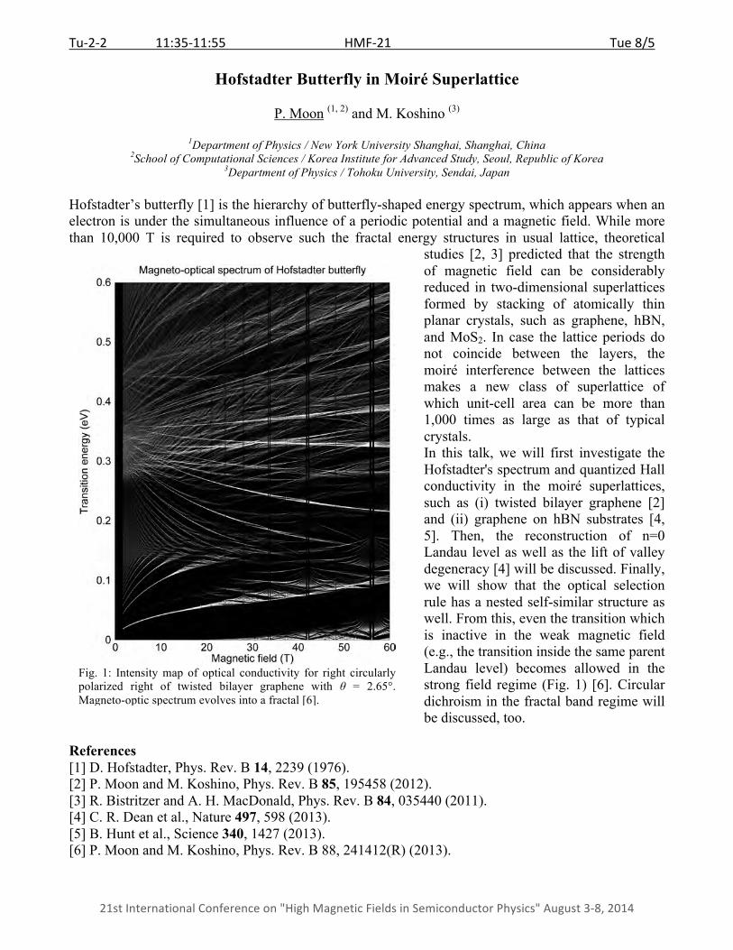
studies [2, 3] predicted that the strength of magnetic field can be considerably reduced in two-dimensional superlattices formed by stacking of atomically thin planar crystals, such as graphene, hBN, and MoS2. In case the lattice periods do not coincide between the layers, the moiré interference between the lattices makes a new class of superlattice of which unit-cell area can be more than 1,000 times as large as that of typical crystals. In this talk, we will first investigate the Hofstadter's spectrum and quantized Hall conductivity in the moiré superlattices, such as (i) twisted bilayer graphene [2] and (ii) graphene on hBN substrates [4, 5]. Then, the reconstruction of n=0 Landau level as well as the lift of valley degeneracy [4] will be discussed. Finally, we will show that the optical selection rule has a nested self-similar structure as well. From this, even the transition which is inactive in the weak magnetic field (e.g., the transition inside the same parent Landau level) becomes allowed in the strong field regime (Fig. 1) [6]. Circular dichroism in the fractal band regime will be discussed, too.
References [1] D. Hofstadter, Phys. Rev. B 14, 2239 (1976). [2] P. Moon and M. Koshino, Phys. Rev. B 85, 195458 (2012). [3] R. Bistritzer and A. H. MacDonald, Phys. Rev. B 84, 035440 (2011). [4] C. R. Dean et al., Nature 497, 598 (2013). [5] B. Hunt et al., Science 340, 1427 (2013). [6] P. Moon and M. Koshino, Phys. Rev. B 88, 241412(R) (2013).
Fig. 1: Intensity map of optical conductivity for right circularly polarized right of twisted bilayer graphene with θ = 2.65°. Magneto-optic spectrum evolves into a fractal [6].
Tu-‐2-‐3 11:55-‐12:15 HMF-‐21 Tue 8/5
21st International Conference on "High Magnetic Fields in Semiconductor Physics" August 3-‐8, 2014
Direct Measurement of the Layer Polarization of Quantum Hall States in Bilayer Graphene
A. F. Young (1), B. Hunt (1), L. Wang (2) , J. Hone (2), C. R. Dean (3) , and R. C. Ashoori (1)
1Massachusetts Institute of Technology, Cambridge, MA, USA
2 Columbia University, New York, NY, USA 3 City College of New York, New York, NY, USA
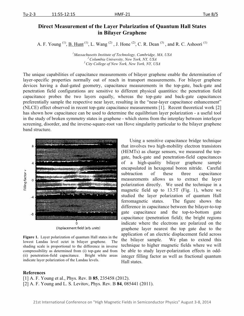
The unique capabilities of capacitance measurements of bilayer graphene enable the determination of layer-specific properties normally out of reach in transport measurements. For bilayer graphene devices having a dual-gated geometry, capacitance measurements in the top-gate, back-gate and penetration field configurations are sensitive to different physical quantities: the penetration field capacitance probes the two layers equally, whereas the top-gate and back-gate capacitances preferentially sample the respective near layer, resulting in the “near-layer capacitance enhancement” (NLCE) effect observed in recent top-gate capacitance measurements [1]. Recent theoretical work [2] has shown how capacitance can be used to determine the equilibrium layer polarization - a useful tool in the study of broken symmetry states in graphene - which stems from the interplay between interlayer screening, disorder, and the inverse-square-root van Hove singularity particular to the bilayer graphene band structure.
Using a sensitive capacitance bridge technique that involves two high-mobility electron transistors (HEMTs) as charge sensors, we measured the top-gate, back-gate and penetration-field capacitances of a high-quality bilayer graphene sample encapsulated in hexagonal boron nitride. Careful subtraction of these three capacitance measurements allows us to extract the layer polarization directly. We used the technique in a magnetic field up to 13.5T (Fig. 1), where we studied the layer polarization of quantum Hall ferromagnetic states. The figure shows the difference in capacitance between the bilayer-to-top gate capacitance and the top-to-bottom gate capacitance (penetration field); the bright regions indicate where the electrons are polarized on the graphene layer nearest the top gate due to the application of an electric displacement field across the bilayer sample. We plan to extend this technique to higher magnetic fields where we will be able to study layer-polarization effects in odd-integer filling factor as well as fractional quantum Hall states.
References [1] A. F. Young et al., Phys. Rev. B 85, 235458 (2012). [2] A. F. Young and L. S. Levitov, Phys. Rev. B 84, 085441 (2011).
Figure 1. Layer polarization of quantum Hall states in the lowest Landau level octet in bilayer graphene. The shading scale is proportional to the difference in inverse compressibility as determined from (i) top-gate and from (ii) penetration-field capacitance. Bright white areas indicate layer polarization of the Landau levels.

Tu-‐3-‐1 13:30-‐14:05 HMF-‐21 Tue 8/5
21st International Conference on "High Magnetic Fields in Semiconductor Physics" August 3-‐8, 2014
Competing Quantum Hall Phases in the Second Landau Level in the Low-Density Limit
Wei Pan
Sandia National Labs, Albuquerque, NM, USA
In recent years, exotic electron physics in the second (N=1) Landau level has been the center of solid state physics research, due to the exciting proposal of using non-Abelian fractional quantum Hall effect (FQHE) states in fault-resistant topological quantum computation [1]. To date, studies of the FQHE physics in the second Landau level have mainly been carried out in the high electron density regime, where the electron mobility is the highest. Only recently, with the advance of high-quality, low-density MBE growth, experiments have been pushed to the low-density regime [2-4], where the electron-electron interactions are strong and the Landau level mixing parameter, defined by k = e2/elB/ħwc, is large. In this talk, we wish to present our recent results obtained in very low-density and high-quality 2DES realized in symmetrically doped GaAs quantum wells. Our result shows that the 7/2 state, a FQHE state in high-density samples, becomes anisotropic in a sample of density n = 5.0×1010 cm-2. In another sample with a lower electron density of 4.1×1010 cm-2, strong 8/3, 5/2 and 7/3 FQHE states were observed. Comparison with previous data suggests that the 5/2 state may be spin-unpolarized in this sample. Our results demonstrate that in the low-density regime the strong electron-electron interactions and large Landau level mixing effect play an important role in competing ground states in the second Landau level. This work was done in collaboration with A. Serafin, J.S. Xia, L. Yin, N.S. Sullivan at the University of Florida/National High Magnetic Field Laboratory, and K.W. Baldwin, K.W. West, L.N. Pfeiffer, and D.C. Tsui at Princeton University. It was supported by the U.S. Department of Energy, Office of Science, Basic Energy Sciences, Materials Sciences and Engineering Division. Sandia National Laboratories is a multi-program laboratory managed and operated by Sandia Corporation, a wholly owned subsidiary of Lockheed Martin Corporation, for the U.S. Department of Energy's National Nuclear Security Administration under Contract No. DE-AC04-94AL85000. References [1] C. Nayak, S.H. Simon, A. Stern, M. Freedman, and S. Das Sarma, Rev. Mod. Phys. 80, 1083 (2008). [2] W. Pan, K. W. Baldwin, K. W. West, L. N. Pfeiffer, and D. C. Tsui, Phys. Rev. Lett. 108, 216804 (2012). [3] G. Liu, C. Zhang, D. C. Tsui, I. Knez, A. Levine, R. R. Du, L. N. Pfeiffer, and K. W. West, Phys. Rev. Lett. 108, 196805 (2012 a). [4] N. Samkharadze, L.N. Pfeiffer, K.W. West, G.A. Csáthy, arXiv: 1302.1444.
Tu-‐3-‐2 14:05-‐14:25 HMF-‐21 Tue 8/5
21st International Conference on "High Magnetic Fields in Semiconductor Physics" August 3-‐8, 2014
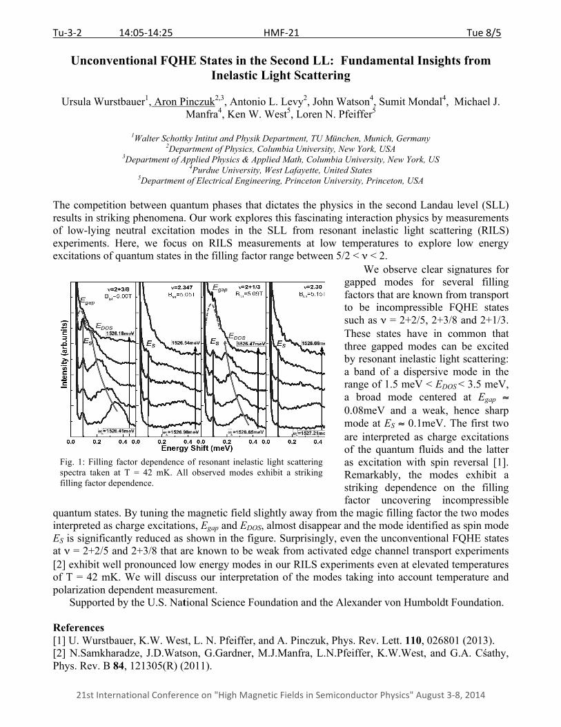
Unconventional FQHE States in the Second LL: Fundamental Insights from Inelastic Light Scattering
Ursula Wurstbauer1, Aron Pinczuk2,3, Antonio L. Levy2, John Watson4, Sumit Mondal4, Michael J.
Manfra4, Ken W. West5, Loren N. Pfeiffer5
1Walter Schottky Intitut and Physik Department, TU München, Munich, Germany 2Department of Physics, Columbia University, New York, USA
3Department of Applied Physics & Applied Math, Columbia University, New York, US 4Purdue University, West Lafayette, United States
5Department of Electrical Engineering, Princeton University, Princeton, USA The competition between quantum phases that dictates the physics in the second Landau level (SLL) results in striking phenomena. Our work explores this fascinating interaction physics by measurements of low-lying neutral excitation modes in the SLL from resonant inelastic light scattering (RILS) experiments. Here, we focus on RILS measurements at low temperatures to explore low energy excitations of quantum states in the filling factor range between 5/2 < ν < 2.
We observe clear signatures for gapped modes for several filling factors that are known from transport to be incompressible FQHE states such as ν = 2+2/5, 2+3/8 and 2+1/3. These states have in common that three gapped modes can be excited by resonant inelastic light scattering: a band of a dispersive mode in the range of 1.5 meV < EDOS < 3.5 meV, a broad mode centered at Egap ≈ 0.08meV and a weak, hence sharp mode at ES ≈ 0.1meV. The first two are interpreted as charge excitations of the quantum fluids and the latter as excitation with spin reversal [1]. Remarkably, the modes exhibit a striking dependence on the filling factor uncovering incompressible
quantum states. By tuning the magnetic field slightly away from the magic filling factor the two modes interpreted as charge excitations, Egap and EDOS, almost disappear and the mode identified as spin mode ES is significantly reduced as shown in the figure. Surprisingly, even the unconventional FQHE states at ν = 2+2/5 and 2+3/8 that are known to be weak from activated edge channel transport experiments [2] exhibit well pronounced low energy modes in our RILS experiments even at elevated temperatures of T = 42 mK. We will discuss our interpretation of the modes taking into account temperature and polarization dependent measurement. Supported by the U.S. National Science Foundation and the Alexander von Humboldt Foundation. References [1] U. Wurstbauer, K.W. West, L. N. Pfeiffer, and A. Pinczuk, Phys. Rev. Lett. 110, 026801 (2013). [2] N.Samkharadze, J.D.Watson, G.Gardner, M.J.Manfra, L.N.Pfeiffer, K.W.West, and G.A. Cśathy, Phys. Rev. B 84, 121305(R) (2011).
Fig. 1: Filling factor dependence of resonant inelastic light scattering spectra taken at T = 42 mK. All observed modes exhibit a striking filling factor dependence.

Tu-‐3-‐3 14:25-‐14:45 HMF-‐21 Tue 8/5
21st International Conference on "High Magnetic Fields in Semiconductor Physics" August 3-‐8, 2014
The Suppression of the Fractional Quantum Hall States of the Second Landau Level by Alloy Disorder
N. Deng(1), G. C. Gardner(2,3), S. Mondal(1,2), E. Kleinbaum(1), M. J. Manfra (1,2,3,4), and G. A. Csáthy(1,2)
1Department of Physics, Purdue University, West Lafayette, IN, USA
2Birck Nanotechnology Center, Purdue University, West Lafayette, IN, USA 3School of Materials Engineering, Purdue University, West Lafayette, Indiana 47907, USA
4School of Electrical and Computer Engineering, Purdue University, West Lafayette, Indiana 47907, USA Disorder is increasingly used in condensed matter physics as a probe of various ground states and it plays a special role in the development and stability of the fractional quantum Hall states. However, quantitative effects of the disorder are not well understood in spite of recent efforts [1,2,3]. We report measurements of the impact of a particular type of short range disorder, specifically alloy disorder, on the ground states of the second Landau level, including on the ν = 5/2 fractional quantum Hall state. Alloy disorder is controlled by the aluminum content x in the AlxGa1−xAs channel in a series of otherwise similar quantum well samples [4]. We find that the ν = 5/2 state is suppressed with alloy scattering [5]. To our surprise, in samples with alloy disorder the ν = 5/2 state appears at significantly reduced mobilities when compared to pristine samples in which alloy disorder is not the dominant scattering mechanism. Our results highlight the distinct roles of the different types of disorder present in these samples, such as the short-range alloy and the long-range Coulomb disorder.
This work was supported by the DOE BES Experimental Condensed Matter Physics and Synthesis and Processing Science programs under the Award No. DE-SC0006671. References [1] W. Pan, N. Masuhara, N. S. Sullivan, K.W. Baldwin, K.W. West, L. N. Pfeiffer, and D. C. Tsui, Phys. Rev. Lett. 106, 206806 (2011). [2] G. Gamez and K. Muraki, Phys. Rev. B 88, 075308 (2013). [3] B.-H. Moon, L. W. Engel, D. C. Tsui, L. N. Pfeiffer, and K. W. West, Phys. Rev. B 89, 075310 (2014). [4] G. C. Gardner, J. D. Watson, S. Mondal, N. Deng, G. A. Csáthy, and M. J. Manfra, Appl. Phys. Lett. 102, 252103 (2013). [5] N. Deng, G. C. Gardner, S. Mondal, E. Kleinbaum, M. J. Manfra, and G. A. Csáthy, Phys. Rev. Lett. 112, 1156804 (2014).
Fig. 1: The dependence of the energy gap Δ5/2 of the ν=5/2 fractional quantum Hall state on inverse mobility 1/µ of our samples (closed symbols) and of alloy-free samples from the literature with densities near 2.9 × 10¹¹/cm2. In our alloy samples the ν=5/2 fractional state survives at surprisingly high 1/µ and, therefore, low µ.

Tu-‐3-‐4 14:45-‐15:20 HMF-‐21 Tue 8/5
21st International Conference on "High Magnetic Fields in Semiconductor Physics" August 3-‐8, 2014
Cooperative Recombination of Electron-Hole Pairs at the Fermi Edge
J.-H. Kim1, K. Cong1, G. T. Noe1, S. A. McGill2, Y. Wang3, A. A. Belyanin3, and J. Kono1
1Department of Electrical and Computer Engineering, Rice University, Houston, Texas 77005, U.S.A. 2National High Magnetic Field Laboratory, Florida State University, Tallahassee, Florida 32310, U.S.A.
3Department of Physics and Astronomy, Texas A&M University, College Station, Texas 77843, U.S.A.
We demonstrate spontaneous appearance of coherence in an optically excited semiconductor quantum well at low temperatures and high magnetic fields [1-3]. We create a quantum-degenerate two-dimensional (2D) electron-hole (e-h) gas with an intense femtosecond laser pulse, and after a certain delay, a picosecond burst of coherent radiation emerges. We interpret this striking phenomenon as a manifestation of superfluorescence (SF), in which a macroscopic polarization spontaneously builds up from an initially incoherent ensemble of excited quantum oscillators and then decays abruptly, producing giant pulses of coherent radiation. SF has been observed in atomic gases, but the present work represents the first observation of SF in a semiconductor, where not only real-photon exchange but also virtual-photon exchange (Coulomb interactions) is responsible for the formation of macroscopic coherence. We found that Coulomb interactions dramatically enhance and modify the collective superradiant decay of the e-h plasma. Unlike typical spontaneous emission from semiconductors, which occurs at the band edge, the observed SF occurs at the quasi-Fermi energy of the highly degenerate carrier distribution, up to 150 meV above the band edge [3]. As the carriers are consumed by ultrafast radiative recombination, the quasi-Fermi energy goes down, and we observe a continuously red-shifting streak of SF at zero magnetic field and a series of sequential SF bursts from higher to lower Landau levels in a magnetic field. This Coulomb enhancement allows the magnitude of the giant dipole to exceed even the maximum possible value for ordinary SF (i.e., the total sum of in-phase oscillations of individual dipoles), making e-h SF even more “super” than atomic SF.
References [1] G. T. Noe et al., Nature Physics 8, 219 (2012). [2] J.-H. Kim et al., Physical Review B 87, 045304 (2013). [3] J.-H. Kim et al., Scientific Reports 3, 3283 (2013).
00"
11"
22"
00"
11"
22"
33"
44"
55"
66"
77"
88"
Fig. 1: Spontaneous appearance of bursts of coherent radiation from a quantum degenerate electron-hole gas in semiconductor quantum wells in high perpendicular magnetic fields.
Tu-‐4-‐1 15:45-‐16:20 HMF-‐21 Tue 8/5
21st International Conference on "High Magnetic Fields in Semiconductor Physics" August 3-‐8, 2014
Robust Quantum Spin Hall Effect in Gated InAs/GaSb Bilayers
Lingjie Du1, Ivan Knez1,2, Gerard Sullivan3, and Rui-Rui Du1
1Rice University, Houston, Texas, USA
2IBM Research – Almaden, San Jose, California, USA 3Teledyne Scientific & Imaging, Thousand Oaks, California, USA
Topological insulators (TIs) are a novel class of materials with nontrivial surface or edge states. Time-reversal symmetry (TRS) protected TIs are characterized by the Z2 topological invariant. We have engineered a TI made of electron-hole bilayers from InAs/GaSb semiconductors, and observed robust helical liquid (HL) edge states with wide conductance plateaus precisely quantized to 2e2/h in a broad temperature range. Remarkably, the quantized plateaus persist to 10T applied in-plane field. In a perpendicular field up to 35T, broken TRS leads to a spatial separation of the movers in the Kramers pair and consequently the intra-pair backscattering phase space vanishes, i.e., the conductance increases from 2e2/h in strong fields manifesting chiral edge transport. Our study presents a compelling case for exotic properties of quantum spin Hall (QSH) effect in InAs/GaSb bilayers.
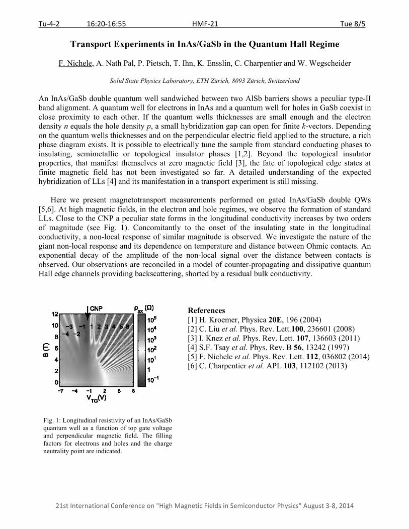
Tu-‐4-‐2 16:20-‐16:55 HMF-‐21 Tue 8/5
21st International Conference on "High Magnetic Fields in Semiconductor Physics" August 3-‐8, 2014
Transport Experiments in InAs/GaSb in the Quantum Hall Regime
F. Nichele, A. Nath Pal, P. Pietsch, T. Ihn, K. Ensslin, C. Charpentier and W. Wegscheider
Solid State Physics Laboratory, ETH Zürich, 8093 Zürich, Switzerland
An InAs/GaSb double quantum well sandwiched between two AlSb barriers shows a peculiar type-II band alignment. A quantum well for electrons in InAs and a quantum well for holes in GaSb coexist in close proximity to each other. If the quantum wells thicknesses are small enough and the electron density n equals the hole density p, a small hybridization gap can open for finite k-vectors. Depending on the quantum wells thicknesses and on the perpendicular electric field applied to the structure, a rich phase diagram exists. It is possible to electrically tune the sample from standard conducting phases to insulating, semimetallic or topological insulator phases [1,2]. Beyond the topological insulator properties, that manifest themselves at zero magnetic field [3], the fate of topological edge states at finite magnetic field has not been investigated so far. A detailed understanding of the expected hybridization of LLs [4] and its manifestation in a transport experiment is still missing.
Here we present magnetotransport measurements performed on gated InAs/GaSb double QWs [5,6]. At high magnetic fields, in the electron and hole regimes, we observe the formation of standard LLs. Close to the CNP a peculiar state forms in the longitudinal conductivity increases by two orders of magnitude (see Fig. 1). Concomitantly to the onset of the insulating state in the longitudinal conductivity, a non-local response of similar magnitude is observed. We investigate the nature of the giant non-local response and its dependence on temperature and distance between Ohmic contacts. An exponential decay of the amplitude of the non-local signal over the distance between contacts is observed. Our observations are reconciled in a model of counter-propagating and dissipative quantum Hall edge channels providing backscattering, shorted by a residual bulk conductivity.
References [1] H. Kroemer, Physica 20E, 196 (2004) [2] C. Liu et al. Phys. Rev. Lett.100, 236601 (2008) [3] I. Knez et al. Phys. Rev. Lett. 107, 136603 (2011) [4] S.F. Tsay et al. Phys. Rev. B 56, 13242 (1997) [5] F. Nichele et al. Phys. Rev. Lett. 112, 036802 (2014) [6] C. Charpentier et al. APL 103, 112102 (2013)
Fig. 1: Longitudinal resistivity of an InAs/GaSb quantum well as a function of top gate voltage and perpendicular magnetic field. The filling factors for electrons and holes and the charge neutrality point are indicated.

We-‐1-‐1 8:45-‐9:05 HMF-‐21 Wed 8/6
21st International Conference on "High Magnetic Fields in Semiconductor Physics" August 3-‐8, 2014
Unconventional Fractional Quantum Hall Effect at ν=4/11 and 5/13
A. Wójs (1), S. Mukherjee (2), S. S. Mandal (2), Y.-H. Wu (3), A. C. Balram (3), J. J. Quinn (4), J. K. Jain (3)
1Institute of Physics, Wrocław University of Technology, Wybrzeże Wyspiańskiego 27, 50-370 Wrocław, Poland 2Department of Theoretical Physics, Indian Association for the Cultivation of Science, Jadavpur, Kolkata 700 032, India
3Department of Physics, 104 Davey Laboratory, Pennsylvania State University, University Park, Pennsylvania 16802, USA 4Department of Physics, University of Tennessee, Knoxville, Tennessee 37996, USA
The fractional quantum Hall effect (FQHE) has now been confirmed at more than 75 filling factors (ν). Majority of these states occur at ν = n/(2pn+1); they are understood as integral quantum Hall states of “composite fermions” (CFs) – particles consisting of electrons binding an even number (2p) of vortices of the many-electron wave function and filling n Landau-like “Λ levels” (ΛLs) in an effective magnetic field B*. But others, like 5/2 or 12/5, depend on complex residual interaction among the CFs. The present work deals with the 4/11 and 5/13 states, discovered a decade ago by Pan et al. [1], and corresponding to the fractional CF filling factors ν*=4/3 and 5/3. We demonstrate that they are genuine fractional quantum Hall states of composite fermions, with incompressibility originating from mutual CF interaction, and with correlations having no analogue in fractional quantum Hall states of electrons. The CF condensation at both ν=4/11 and 5/13 is predominantly due to pair (CF-CF) interaction [2] within the second ΛL, which is dominated by strong repulsion at relative pair angular momentum m=3. This yields a peculiar form of correlation among the CFs, exemplifying unconventional mechanism for incompressibility [3]. The ΛL mixing, giving rise to effective triplet interaction among CFs in the second ΛL, also plays a role (breaks particle-hole symmetry in ΛLs, causing different gaps at ν=4/11 and 5/13. Some insight into the above physics came from ‘standard’ exact diagonalization for electrons (fully including ΛL mixing, but with feasible dimensions ≤109 limiting the spectra to N≤16 electrons or N*≤6 CFs in the second ΛL) and for CFs with effective pair interaction (ignoring ΛL mixing, but allowing N*≤16). However, the crucial evidence has come from ‘CF diagonalization’, which provided reliable spectra including ΛL mixing for N≤28 (N*≤9) at ν=4/11 and N≤31 (N*≤12) at ν=5/13 (see Fig.1). The unconventional 4/11 state is characterized by distinct shift 7 on a sphere, a unique correlation function and quasiparticle and quasihole densities, e/3 charge, Abelian statistics, edge with multiple channels and no backward neutral modes. Regarding spin, transition to unpolarized conventional phase is predicted at a low spin gap. The 4/11 state will also be contrasted with 7/3 [4], where electrons in the second Landau level form a Laughlin-like state. References [1] W. Pan et al., Phys. Rev. Lett. 90, 016801 (2003). [2] A. Wójs, K.-S. Yi, and J. J. Quinn, Phys. Rev. B 69, 205322 (2004). [3] S. Mukherjee, S. S. Mandal, Y.-H. Wu, A. Wójs, J. K. Jain, Phys. Rev. Lett. 112, 016801 (2014). [4] A. C. Balram, Y.-H. Wu, G. J. Sreejith, A. Wójs, J. K. Jain, Phys. Rev. Lett. 110, 186801 (2013).
Fig. 1: Energy spectra (energy E vs. angular momentum L) at ν=4/11 and 5/13. Circles – CF diagonalization; dashes – exact diagonalization in full Hilbert space. Figure from [3].
We-‐1-‐2 9:05-‐9:25 HMF-‐21 Wed 8/6
21st International Conference on "High Magnetic Fields in Semiconductor Physics" August 3-‐8, 2014
Bulk Thermoelectric and Thermodynamic Probes of non-Abelian Anyons in Topological States of Matter
Kun Yang,1 Y. Barlas,1 M. Freedman,2 G. Gervais,3 B. I. Halperin,4 and S. Yamamoto1
1National High Magnetic Field Lab and Physics Department, Florida State University, Tallahassee, FL 32306, USA
2 Microsoft Research, Station Q, Elings Hall, University of California, Santa Barbara, CA 93106, USA 3 Department of Physics, McGill University, Montreal, H3A 2T8, CANADA
3 Department of Physics, Harvard University, Cambridge, Massachusetts 02138, USA
Topological states of matter support quasiparticle excitations with fractional charge and possibly exotic statistics of the non-Abelian type, known as non-Abelian anyons. Most current experimental attempts to reveal such exotic statistics focus on interference involving edge transport. After a brief introduction of topological states, in this presentation we will discuss how one can reveal the non-Abelian quasiparticle statistics using bulk probes. We show that bulk thermopower is a promising way to detect their non-Abelian nature, and measure the quantum dimension (a key parameter that quantifies non-Abelian statistics) of these anyons [1]. This method is particularly effective in the Corbino geometry [2]. We also demonstrate a novel cooling effect associated with them [3,4]. We discuss application of these ideas to the specific candidate system of fractional quantum Hall liquid at filling factor 5/2 [1,2,3], and topological insulator-superconductor hybrid systems [4]. Some of the predicted behavior has been observed in recent experiments [5,6], which will also be discussed. This body of work has also motivated further theoretical efforts of using thermal probes to study non-Abelian anyons [7].
References [1] Kun Yang and B. I. Halperin, Phys. Rev. B 79, 115317 (2009). [2] Y. Barlas and Kun Yang, Phys. Rev. B 85, 195107 (2012). [3] G. Gervais and Kun Yang, Phys. Rev. Lett.105, 086801 (2010). [4] S. Yamamoto, M. Freedman, Y. Barlas, Phys. Rev. B 84, 104503 (2011). [5] W. E. Chickering, J. P. Eisenstein, L. N. Pfeiffer, and K. W. West, Phys. Rev. B 87, 075302 (2013). [6] Shuhei Kobayakawa, Akira Endo, and Yasuhiro Iye, J. Phys. Soc. Jpn. 82, 053702 (2013). [7] N. d’Ambrumenil and R. H. Morf, Thermopower in the Quantum Hall Regime, Phys. Rev. Lett. 111, 136 (2013); Chang-Yu Hou, Y. Barlas, K. Shtengel, Adiabatic cooling of Majorana zero-modes in topological superconductors, eprint arXiv:1310.1418.

We-‐1-‐3 9:25-‐9:45 HMF-‐21 Wed 8/6
21st International Conference on "High Magnetic Fields in Semiconductor Physics" August 3-‐8, 2014
Experimental Evidence for Particle-Hole Symmetry Breaking in the Ballistic Transport of Fully Spin-Polarized ν = 1/2 Composite Fermions
D. Kamburov, M.A. Mueed, M. Shayegan, L. N. Pfeiffer, K. W. West, K. W. Baldwin
Department of Electrical Engineering, Princeton University, USA
The physics of an interacting two-dimensional electron system (2DES) at low temperatures and strong perpendicular magnetic field is elegantly described by the composite fermion (CF) formalism in which an even number of flux quanta is attached to each electron in high magnetic field. A fundamental property of CFs at half-filled Landau levels is that they occupy a Fermi sea and therefore possess a Fermi contour. We have recently probed this Fermi contour in a number of commensurability experiments performed on samples with a unidirectional periodic potential modulation in the 2D plane [1-3]. In these experiments, when the quasi-classical CF cyclotron orbit diameter matches an integer multiple of the period, a resistance minimum is expected. Here we report the observation of a pronounced asymmetry in the magnetic field positions of the commensurability resistance minima of fully spin-polarized CFs with respect to the field at ν = ½ (see Fig. 1). The asymmetry is observed across a wide range of 2D densities and modulation periods. We can explain the asymmetry quantitatively if we assume that the CFs are fully spin-polarized and their density is equal to the density of the minority carriers in the lowest, spin-resolved Landau level (LL), namely the density of electrons when ν < ½ and of holes when ν > ½. Our results provide direct evidence that CFs are formed by pairing up of the minority carriers in the lowest spin-resolved LL with flux quanta. They further indicate a breaking of the particle-hole symmetry for spin-polarized CFs near ν = ½. References: [1] Kamburov et al., Phys. Rev. Lett. 109, 236401 (2012) [2] Kamburov et al., Phys. Rev. Lett. 110, 206801 (2013) [3] Kamburov et al., Phys. Rev. B 89, 085304 (2014)
FIG. 1: Composite fermion commensurability oscillations near ν = ½ in a GaAs 2DES subjected to a unidirectional lateral modualtion of period 200 nm. The solid vertical tick marks indicate the expected positions of the resistance mimina if we assume the CF density (nCF) equals the 2DES density (n); these marks, which are symmetric with respect to the field position of ν = ½ (B = 14.4 T), match very well the observed resistance minima for ν < ½ (B > 14.4 T) but not for ν > ½ (B < 14.4 T). On the other hand, the dashed veritcal thick marks, which are based on the assumption that nCF equals the density of the minority carriers in the lowest spin-resolved Landau level [nCF = ((1-ν)/ν)n], i.e., holes for ν > ½, are in excellent agreement with the experimental data. Note that for ν < ½ the density of minority carriers (electrons) in the lowest spin-resolved Landau level is equal to n so the dashed and solid vertical marks coincide.
(a) (b)
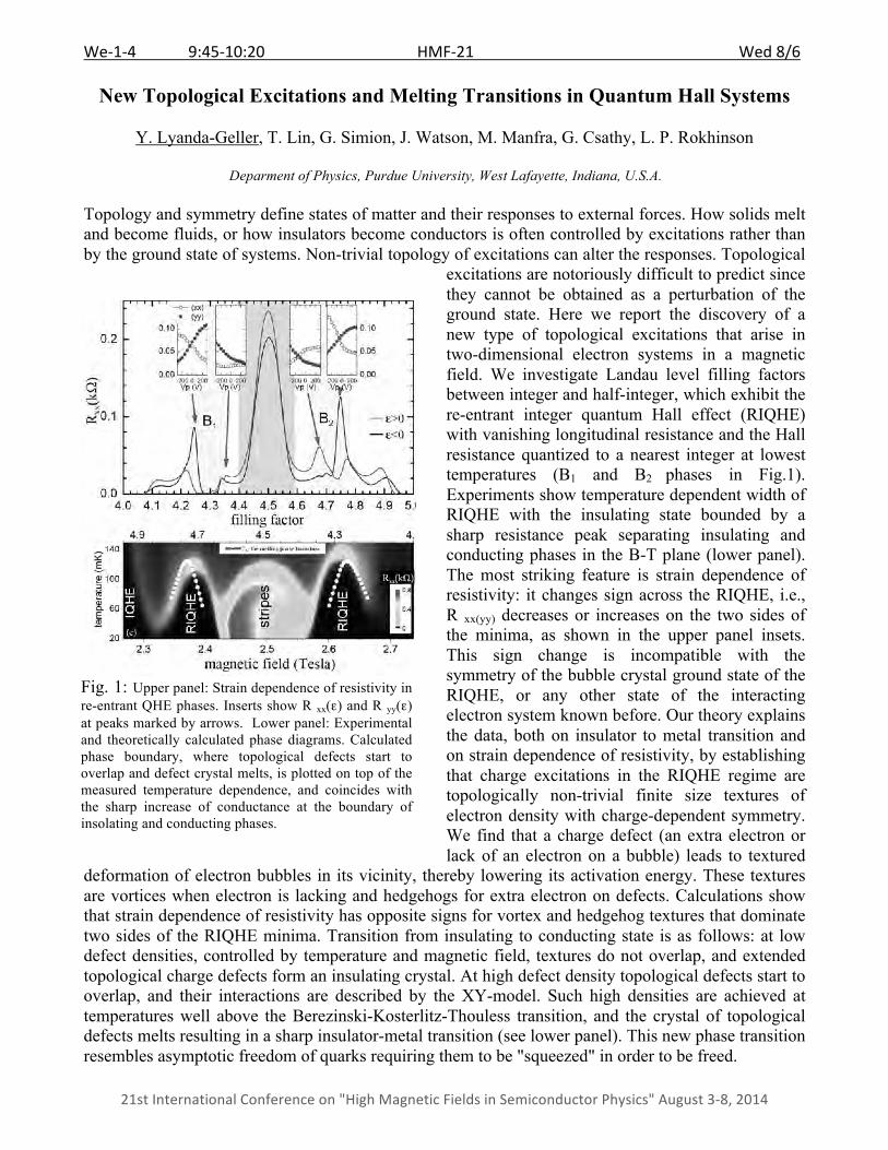
We-‐1-‐4 9:45-‐10:20 HMF-‐21 Wed 8/6
21st International Conference on "High Magnetic Fields in Semiconductor Physics" August 3-‐8, 2014
New Topological Excitations and Melting Transitions in Quantum Hall Systems
Y. Lyanda-Geller, T. Lin, G. Simion, J. Watson, M. Manfra, G. Csathy, L. P. Rokhinson
Deparment of Physics, Purdue University, West Lafayette, Indiana, U.S.A. Topology and symmetry define states of matter and their responses to external forces. How solids melt and become fluids, or how insulators become conductors is often controlled by excitations rather than by the ground state of systems. Non-trivial topology of excitations can alter the responses. Topological
excitations are notoriously difficult to predict since they cannot be obtained as a perturbation of the ground state. Here we report the discovery of a new type of topological excitations that arise in two-dimensional electron systems in a magnetic field. We investigate Landau level filling factors between integer and half-integer, which exhibit the re-entrant integer quantum Hall effect (RIQHE) with vanishing longitudinal resistance and the Hall resistance quantized to a nearest integer at lowest temperatures (B1 and B2 phases in Fig.1). Experiments show temperature dependent width of RIQHE with the insulating state bounded by a sharp resistance peak separating insulating and conducting phases in the B-T plane (lower panel). The most striking feature is strain dependence of resistivity: it changes sign across the RIQHE, i.e., R xx(yy) decreases or increases on the two sides of the minima, as shown in the upper panel insets. This sign change is incompatible with the symmetry of the bubble crystal ground state of the RIQHE, or any other state of the interacting electron system known before. Our theory explains the data, both on insulator to metal transition and on strain dependence of resistivity, by establishing that charge excitations in the RIQHE regime are topologically non-trivial finite size textures of electron density with charge-dependent symmetry. We find that a charge defect (an extra electron or lack of an electron on a bubble) leads to textured
deformation of electron bubbles in its vicinity, thereby lowering its activation energy. These textures are vortices when electron is lacking and hedgehogs for extra electron on defects. Calculations show that strain dependence of resistivity has opposite signs for vortex and hedgehog textures that dominate two sides of the RIQHE minima. Transition from insulating to conducting state is as follows: at low defect densities, controlled by temperature and magnetic field, textures do not overlap, and extended topological charge defects form an insulating crystal. At high defect density topological defects start to overlap, and their interactions are described by the XY-model. Such high densities are achieved at temperatures well above the Berezinski-Kosterlitz-Thouless transition, and the crystal of topological defects melts resulting in a sharp insulator-metal transition (see lower panel). This new phase transition resembles asymptotic freedom of quarks requiring them to be "squeezed" in order to be freed.
Fig. 1: Upper panel: Strain dependence of resistivity in re-entrant QHE phases. Inserts show R xx(ε) and R yy(ε) at peaks marked by arrows. Lower panel: Experimental and theoretically calculated phase diagrams. Calculated phase boundary, where topological defects start to overlap and defect crystal melts, is plotted on top of the measured temperature dependence, and coincides with the sharp increase of conductance at the boundary of insolating and conducting phases.
We-‐1-‐5 10:20-‐10:40 HMF-‐21 Wed 8/6
21st International Conference on "High Magnetic Fields in Semiconductor Physics" August 3-‐8, 2014
Quantum Depinning in Two-dimensional Wigner Solids in Zero Magnetic Field
J. Huang1, L. Pfeiffer2, K. West2
1. Department of Physics, Wayne State University, Detroit, MI, 48201 USA 2. Department of Electrical Engineering, Princeton University, Princeton, NJ 08544, USA
In strongly correlated electron systems, extraordinary quantum manybody states emerge in response to the substantial inter-particle Coulomb interaction. The most prominent example is the Wigner crystallization (WC) as a demonstration of dominating interaction effects [1,2]. The classical version of WC, with the Coulomb energy Ec similar to the Debye temperature ΘD, has been demonstrated in electrons on a helium surface. On the other hand, the quantum version, with Ec<<ΘD, has not been previously observed in a zero magnetic field. Much effort has been made to obtain experimental evidence in the fractional quantum Hall regime (FQH) in high magnetic fields in which the enhanced interaction effect is achieved by suppressing the kinetic energy. However, the high magnetic field inevitably modifies the electron wavefunctions which, in turn, radically alter the manybody states. Therefore, a definitive equivalence between the observed reentrant insulating phases and the Wigner crystal has not been established. In a zero magnetic field, the wavefuctions are fully preserved. The experiments then require systems with highest purity and measured in a limit of extremely dilute charge concentrations, which compose tremendous challenges in terms of fabrication [3] and extremely low noise measurement.
We have adopted a novel type of ultra-high purity, undoped 2D systems in GaAs/AlGaAs HIGFET [3] with much suppressed disorder. We have successfully fabricated and measured many undoped p-channel HIGFET samples that have demonstrated outstanding charge mobility and record low charge densities down to 6×108 cm-2, corresponding to a mean charge spacing of 0.5 micrometer. In this work, setting a 2D hole density to 2.8×109 cm-2, we have performed dc V-I measurement with signal resolutions of 0.1 pA and 0.7 µV, for a temperature (T) range from 29 to 40 mK. Compared to most previous results, this low charge density corresponds to a genuine interaction-driven limit with rs > 45. For T<40 mK, we have observed a threshold behavior that is similar to those previously found for electrons on helium and charge density waves (CDW). Remarkably, despite of the much suppressed disorder, we observed an enormous pinning, 200 times stronger than previous finding, indicated by an extremely small threshold current of 2.5 pA in the presence of a depinning threshold field of 170 µV which is only 1/10,000 of the classical limit ( -pinning frequency and - lattice constant). Compared to all previous results from the threshold we observed, this current threshold is only 1/1,000 to 1/1,000,000 of the magnitudes for the electrons on helium, GaAs in high fields, and CDW cases. Therefore, it is a strong indication of a rigorously pinned quantum WC, instead of a Wigner glass or an Anderson insulator. In addition, voltage oscillations with negative differential resistance (NDR), a feature that is almost identical to the electrons on helium, are observed. It confirms the coexistence of a pinned Wigner crystal along with ordered edge current states. Moreover, the T-dependence of the oscillations indicates a melting point well below the classical estimate. Multiple data features, such as the remarkably small yet finite threshold in the limit of T→0, the melting of the WC well below the classical point, and the absence of hysteresis, suggests a quantum depinning mechanism [4] rather than a classical one. A manybody quantum tunneling mechanism based on the creation of quantum dislocations [2] will be discussed. References [1] E. P. Wigner, Phys. Rev. 46, 1002 (1934); [2] S. T. Chui, Physics of the Electron Solid, 157146106X / 9781571461063; [3] Jian Huang, D. C. Tsui, L. N. Pfeiffer, K. W. West, IJMPB 21, 1219 (2007); [4] Jian Huang, L. N. Pfeiffer, K. W. West, Submitted to Science (2014); available @ Arxiv:1306.4196.
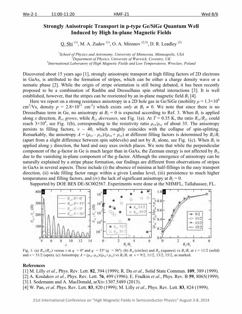
We-‐2-‐1 11:00-‐11:20 HMF-‐21 Wed 8/6
21st International Conference on "High Magnetic Fields in Semiconductor Physics" August 3-‐8, 2014
Strongly Anisotropic Transport in p-type Ge/SiGe Quantum Well Induced by High In-plane Magnetic Fields
Q. Shi (1), M. A. Zudov (1), O. A. Mironov (2,3), D. R. Leadley (2)
1School of Physics and Astronomy, University of Minnesota, Minneapolis, USA
2Department of Physics, University of Warwick, Coventry, UK 3International Laboratory of High Magnetic Fields and Low Temperatures, Wroclaw, Poland
Discovered about 15 years ago [1], strongly anisotropic transport at high filling factors of 2D electrons in GaAs, is attributed to the formation of stripes, which can be either a charge density wave or a nematic phase [2]. While the origin of stripe orientation is still being debated, it has been recently proposed to be a combination of Rashba and Dresselhaus spin orbital interactions [3]. It is well established, however, that the stripes can be reoriented by an in-plane magnetic field B|| [4]. Here we report on a strong resistance anisotropy in a 2D hole gas in Ge/SiGe (mobility µ = 1.3×106 cm2/Vs, density p = 2.8×1011 cm-2) which exists only at B|| ≠ 0. We note that since there is no Dresselhaus term in Ge, no anisotropy at B|| = 0 is expected according to Ref. 3. When B|| is applied along x direction, Rxx grows, while Ryy decreases, see Fig. 1(a). At T = 0.35 K, the ratio Rxx/Ryy could reach 3×10⁴, see Fig. 1(b), corresponding to the resistivity ratio ρxx/ρyy of about 35. The anisotropy persists to filling factors, ν ~ 40, which roughly coincides with the collapse of spin-splitting. Remarkably, the anisotropy A = (ρxx – ρyy)/(ρxx + ρyy) at different filling factors is determined by Bx/Bz (apart from a slight difference between spin sublevels) and not by Bx alone, see Fig. 1(c). When B|| is applied along y direction, the hard and easy axes switch places. We note that while the perpendicular component of the g-factor in Ge is much larger than in GaAs, the Zeeman energy is not affected by B||, due to the vanishing in-plane component of the g-factor. Although the emergence of anisotropy can be naturally explained by a stripe phase formation, our findings are different from observations of stripes in GaAs in several aspects. These include (i) the absence of minima at half-fillings in the easy transport direction, (ii) wide filling factor range within a given Landau level, (iii) persistence to much higher temperatures and filling factors, and (iv) the lack of significant anisotropy at B|| = 0. Supported by DOE BES DE-SC002567. Experiments were done at the NHMFL, Tallahassee, FL.
Fig. 1: (a) Rxx (Ryy) versus ν at q = 0º and q = 53º (q = 56º). (b) Rxx (circles) and Ryy (squares) vs Bx/Bz at ν = 11/2 (solid) and ν = 31/2 (open). (c) Anisotropy A = (ρxx–ρyy)/(ρxx+ρyy) vs Bx/Bz at ν = 9/2, 11/2, 13/2, 15/2, as marked. References [1] M. Lilly et al., Phys. Rev. Lett. 82, 394 (1999); R. Du et al., Solid State Commun. 109, 389 (1999). [2] A. Koulakov et al., Phys. Rev. Lett. 76, 499 (1996); E. Fradkin et al., Phys. Rev. B 59, 8065(1999). [3] I. Sodemann and A. MacDonald, arXiv:1307.5489 (2013). [4] W. Pan, et al. Phys. Rev. Lett. 83, 820 (1999); M. Lilly et al., Phys. Rev. Lett. 83, 824 (1999).
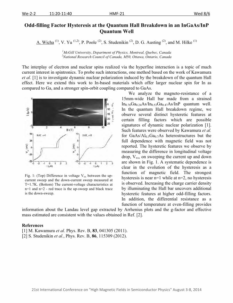
We-‐2-‐2 11:20-‐11:40 HMF-‐21 Wed 8/6
21st International Conference on "High Magnetic Fields in Semiconductor Physics" August 3-‐8, 2014
Odd-filling Factor Hysteresis at the Quantum Hall Breakdown in an InGaAs/InP Quantum Well
A. Wicha (1), V. Yu (1,2), P. Poole (2), S. Studenikin (2), D. G. Austing (2), and M. Hilke (1)
1McGill University, Department of Physics, Montreal, Quebec, Canada 2National Research Council of Canada, M50, Ottawa, Ontario, Canada
The interplay of electron and nuclear spins realized via the hyperfine interaction is a topic of much current interest in spintronics. To probe such interactions, one method based on the work of Kawamura et al. [1] is to investigate dynamic nuclear polarization induced by the breakdown of the quantum Hall effect. Here we extend this work to In-based materials which offer larger nuclear spin for In as compared to Ga, and a stronger spin-orbit coupling compared to GaAs.
We analyze the magneto-resistance of a 15mm-wide Hall bar made from a strained In0.76Ga0.24As/In0.53Ga0.47As/InP quantum well. In the quantum Hall breakdown regime, we observe several distinct hysteretic features at certain filling factors which are possible signatures of dynamic nuclear polarization [1]. Such features were observed by Kawamura et al. for GaAs/Al0.3Ga0.7As heterostructures but the full dependence with magnetic field was not reported. The hysteretic features we observe by measuring the difference in longitudinal voltage drop, Vxx, on sweeping the current up and down are shown in Fig. 1. A systematic dependence is clear in the evolution of the hysteresis as a function of magnetic field. The strongest hysteresis is near n=1 while at n=2, no hysteresis is observed. Increasing the charge carrier density by illuminating the Hall bar uncovers additional hysteretic features at higher odd-filling factors. In addition, the differential resistance as a function of temperature at even-filling provides
information about the Landau level gap extracted by Arrhenius plots and the g-factor and effective mass estimated are consistent with the values obtained in Ref. [2]. References [1] M. Kawamura et al. Phys. Rev. B, 83, 041305 (2011). [2] S. Studenikin et al., Phys. Rev. B, 86, 115309 (2012).
Fig. 1: (Top) Difference in voltage Vxx between the up-current sweep and the down-current sweep measured at T=1.7K. (Bottom) The current-voltage characteristics at n=1 and n=2 - red trace is the up-sweep and black trace is the down-sweep.

We-‐2-‐3 11:40-‐12:00 HMF-‐21 Wed 8/6
21st International Conference on "High Magnetic Fields in Semiconductor Physics" August 3-‐8, 2014
High Hall-mobilities in Field-effect Transistors Based on Mechanically Exfoliated Few-layered p-WSe2 on SiO2
N. R. Pradhan (1), D. Rhodes (1), S. Memaran (1), J. M. Poumirol (1), D. Smirnov (1), S.
Talapatra (2), S. Feng (3), N. Perea-Lopez (3), A. L. Elias (3), M. Terrones (3), P. M. Ajayan (4), and L. Balicas (1),
1National High Magnetic Field Laboratory, Florida State University, Tallahassee-FL 32310, USA
2 Physics Department, Southern Illinois University, Carbondale-IL 62901-4401, USA 3Department of Physics, Department of Materials Science and Engineering and Materials Research Institute, The Pennsylvania State University, University Park, PA 16802, USA
4Department of Mechanical Engineering and Materials Science, Rice University, Houston, TX 77005 USA
Here, we present a comparison between field-effect and Hall mobilities in field-effect transistors based on few-layered WSe2 on SiO2. Without dielectric engineering, we observe maximum hole mobilities approaching 350 cm2/Vs at T = 300 K, but (as in graphene) the mobilities tend to decrease as the number of carriers increase. The hole Hall mobility mH reaches 650 cm2/Vs as the T is lowered below T = 150 K, indicating that insofar WSe2-based field-effect transistors (FETs) display the largest Hall mobilities among the transition metal dichalcogenides (TMDs). The gate capacitance, as extracted from the Hall-effect, indicates the presence of spurious, excess charges within the channel, which are likely to be a major source of scattering for all TMDs based FETs. We argue that improvement in fabrication protocols through, for example, the use of a high k-dielectrics to minimize the role of these spurious charges, might produce WSe2-based FETs displaying room temperature drift mobilities in excess of 500 cm2/Vs, therefore comparable to p-doped Si. High drive currents and higher mobilities suggests that multi-layered, hole-doped WSe2 might be a more suitable candidate for high performance opto-electronics than MoS2. This work is supported by the U.S. Army Research Office MURI grant W911NF-11-1-0362. The NHMFL is supported by NSF through NSF-DMR-0084173 and the State of Florida.
Fig. 1. Micrograph of one of our WSe2 based field-effect transistors, showing the current contacts and voltage contacts used for resistivity (rxx) and Hall-effect (Rxy) measurements. Field H was applied perpendicularly to the plane. Right panel: Hall response Rxy as a function of H for several values of the gate voltage. Red lines are linear fits from which we extract the Hall constant RH and the Hall mobilities mH = RH/rxx.

We-‐2-‐4 12:00-‐12:20 HMF-‐21 Wed 8/6
21st International Conference on "High Magnetic Fields in Semiconductor Physics" August 3-‐8, 2014
High Magnetic Field Studies on Orientationally Ordered Fluid Phases
J.T. Gleeson (1), S.N. Sprunt (1), A. Jakli (1)
1Kent State University, Kent, OH, USA
Orientationally ordered fluids, of which liquid crystals are the best known example, are particularly susceptible to external fields, and high magnetic fields are especially effective. This is because when the orientational order is short-range, a high field is can substantially enhance this order. Furthermore, even when the order is long-range, high fields can control the principal axes of the order parameter tensor. We have applied these tools to a wide variety of classes of ordered fluids, including traditional and exotic thermotropic liquid crystals, lyotropic chromonic, “stacking” fluids, microtubules formed by self-assembled tubulin proteins, and suspensions of anisotropic nanoparticles.
In these materials, measurements of classical magneto-optical responses, such as the Cotton-Mouton effect, are especially valuable. This effect, in the vicinity of a phase transition, is dominated by order parameter fluctuations and reveals otherwise unavailable details of the phase transition character. We utilize this effect to study various classes of complex fluids and use high fields to accurately probe their propensity to order, and the stability limits of their isotropic, high-symmetry states.1
In addition, magnetic fields exert a torque on the direction of orientational order that increases with H2. This leverage enables an accurate extrapolation to infinite field, which we have used to detect the presence of exotic types of order having two rather than a single symmetry axis.2 Furthermore, we report that for fields exceeding 20T, we can suppress the formation of an exotic liquid-crystalline state that has been long-predicted but only recently discovered. This state is shows spontaneous, short-range chiral symmetry, even though it is comprised of achiral molecules. This result leads to the first ever measurement of the relevant elastic moduli of this new state of matter.3 We also report studies on biologically compatible chromonic liquid crystals. Under high fields we found these materials to exhibit a fascinating and exotic hybrid magneto-optic response: a combination of field-induced linear and circular birefringence (but zero linear and circular dichroism).4
Acknowledgments: Supported by the NSF (DMR-0606160, DMR-0964765 and DMR-1307674).
1 P.K. Challa, O. Curtiss, J.C. Williams, R. Twieg, J. Toth, S. McGill, A. Jakli, J.T. Gleeson and S.N. Sprunt, Phys. Rev. E, 86, 11708 (2012). 2 T. Ostapenko, C. Zhang, S.N. Sprunt, A. Jakli, J.T. Gleeson, Phys. Rev. E, 84, 21705 (2011). 3 P.K. Challa, V. Borschch, O. Parri, S.N. Sprunt, O.D. Lavrentovich, J.T. Gleeson and A. Jakli, Phys Rev. Lett., submitted, (2014). 4 T. Ostapenko, Y.A. Nastishin, P.J. Collings, S.N. Sprunt, O.D. Lavrentovich, and J.T. Gleeson, Soft. Matt., 9, 9487 (2013).
!
Figure 1 Induced birefringence vs H2 for 2.5 wt% Bordeaux dye in water. As the temperature is decreased, the deviation from linear Cotton-Mouton behavior becomes ever more pronounced.
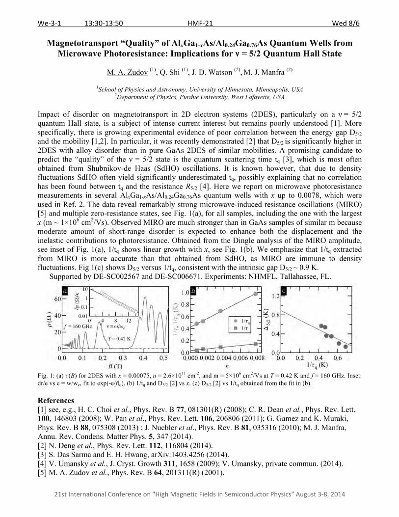
We-‐3-‐1 13:30-‐13:50 HMF-‐21 Wed 8/6
21st International Conference on "High Magnetic Fields in Semiconductor Physics" August 3-‐8, 2014
Magnetotransport “Quality” of AlxGa1-xAs/Al0.24Ga0.76As Quantum Wells from Microwave Photoresistance: Implications for ν = 5/2 Quantum Hall State
M. A. Zudov (1), Q. Shi (1), J. D. Watson (2), M. J. Manfra (2)
1School of Physics and Astronomy, University of Minnesota, Minneapolis, USA
2Department of Physics, Purdue University, West Lafayette, USA Impact of disorder on magnetotransport in 2D electron systems (2DES), particularly on a ν = 5/2 quantum Hall state, is a subject of intense current interest but remains poorly understood [1]. More specifically, there is growing experimental evidence of poor correlation between the energy gap D5/2 and the mobility [1,2]. In particular, it was recently demonstrated [2] that D5/2 is significantly higher in 2DES with alloy disorder than in pure GaAs 2DES of similar mobilities. A promising candidate to predict the “quality” of the ν = 5/2 state is the quantum scattering time tq [3], which is most often obtained from Shubnikov-de Haas (SdHO) oscillations. It is known however, that due to density fluctuations SdHO often yield significantly underestimated tq, possibly explaining that no correlation has been found between tq and the resistance R5/2 [4]. Here we report on microwave photoresistance measurements in several AlxGa1-xAs/Al0.24Ga0.76As quantum wells with x up to 0.0078, which were used in Ref. 2. The data reveal remarkably strong microwave-induced resistance oscillations (MIRO) [5] and multiple zero-resistance states, see Fig. 1(a), for all samples, including the one with the largest x (m ~ 1×106 cm2/Vs). Observed MIRO are much stronger than in GaAs samples of similar m because moderate amount of short-range disorder is expected to enhance both the displacement and the inelastic contributions to photoresistance. Obtained from the Dingle analysis of the MIRO amplitude, see inset of Fig. 1(a), 1/tq shows linear growth with x, see Fig. 1(b). We emphasize that 1/tq extracted from MIRO is more accurate than that obtained from SdHO, as MIRO are immune to density fluctuations. Fig 1(c) shows D5/2 versus 1/tq, consistent with the intrinsic gap D5/2 ~ 0.9 K.
Supported by DE-SC002567 and DE-SC006671. Experiments: NHMFL, Tallahassee, FL.
Fig. 1: (a) r (B) for 2DES with x = 0.00075, n = 2.6×1011 cm-2, and m = 5×106 cm2/Vs at T = 0.42 K and f = 160 GHz. Inset: dr/e vs e = w/wc, fit to exp(-e/ftq). (b) 1/tq and D5/2 [2] vs x. (c) D5/2 [2] vs 1/tq obtained from the fit in (b). References [1] see, e.g., H. C. Choi et al., Phys. Rev. B 77, 081301(R) (2008); C. R. Dean et al., Phys. Rev. Lett. 100, 146803 (2008); W. Pan et al., Phys. Rev. Lett. 106, 206806 (2011); G. Gamez and K. Muraki, Phys. Rev. B 88, 075308 (2013) ; J. Nuebler et al., Phys. Rev. B 81, 035316 (2010); M. J. Manfra, Annu. Rev. Condens. Matter Phys. 5, 347 (2014). [2] N. Deng et al., Phys. Rev. Lett. 112, 116804 (2014). [3] S. Das Sarma and E. H. Hwang, arXiv:1403.4256 (2014). [4] V. Umansky et al., J. Cryst. Growth 311, 1658 (2009); V. Umansky, private commun. (2014). [5] M. A. Zudov et al., Phys. Rev. B 64, 201311(R) (2001).
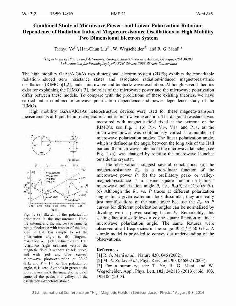
We-‐3-‐2 13:50-‐14:10 HMF-‐21 Wed 8/6
21st International Conference on "High Magnetic Fields in Semiconductor Physics" August 3-‐8, 2014
Combined Study of Microwave Power- and Linear Polarization Rotation- Dependence of Radiation Induced Magnetoresistance Oscillations in High Mobility
Two Dimensional Electron System
Tianyu Ye(1), Han-Chun Liu(1), W. Wegscheider(2) and R. G. Mani(1)
1Department of Physics and Astronomy, Georgia State University, Atlanta, Georgia, USA 30303 2Laboratorium für Festkörperphysik, ETH Zürich, 8093 Zürich, Switzerland
The high mobility GaAs/AlGaAs two dimensional electron system (2DES) exhibits the remarkable radiation-induced zero resistance states and associated radiation-induced magnetoresistance oscillations (RIMOs)[1,2], under microwave and terahertz wave excitation. Although several theories exist for explaining the RIMO’s[3], the roles of the microwave power and the microwave polarization differ between these models. To compare with the predictions of these existing theories, we have carried out a combined microwave polarization dependence and power dependence study of the RIMOs.
High mobility GaAs/AlGaAs heterostructure devices were used for these magneto-transport measurements at liquid helium temperatures under microwave excitation. The diagonal resistance was
measured with magnetic field fixed at the extrema of the RIMO’s, see Fig. 1 (b) P1-, V1-, V1+ and P1+, as the microwave power was continuously varied at a number of microwave polarization angles. The linear polarization angle, which is defined as the angle between the long axis of the Hall bar and the microwave antenna in the microwave launcher, see Fig. 1 (a), was changed by rotating the microwave launcher outside the cryostat. The observations suggest several conclusions: (a) the magnetoresistance Rxx is a non-linear function of the microwave power P. (b) the oscillatory peak- or valley- magnetoresistance is a cosine square function of linear microwave polarization angle θ, i.e., Rxx(θ)=A±Ccos2(θ−θ0). (c) Although the Rxx vs. P traces at different polarization angles for a given extremum look dissimilar, they are really just manifestations of the same trace because the Rxx vs P curves for different polarization angles can be normalized by dividing with a power scaling factor Ps. Remarkably, this scaling factor also follows a cosine square function of linear microwave polarization angle. The same features were observed at all frequencies in the range 30 ≤ f ≤ 50 GHz. A simple model is provided to convey our understanding of the observations. References [1] R. G. Mani et al., Nature 420, 646 (2002). [2] M. A. Zudov et al., Phys. Rev. Lett. 90, 046807 (2003). [3] For a summary, see: T. Ye, R. G. Mani, and W. Wegscheider, Appl. Phys. Lett. 102, 242113 (2013); ibid. 103, 192106 (2013).
Fig. 1: (a) Sketch of the polarization orientation in the measurement. Here, the antenna and the microwave launcher rotate clockwise with respect of the long axis of Hall bar sample to set the polarization angle θ. (b) Diagonal resistance Rxx (left ordinate) and Hall resistance (right ordinate) versus the magnetic field B without (black curve) and with (red- and blue- curves) microwave photo-excitation at 33.62 GHz and T = 1.5 K. The polarization angle, θ, is zero. Symbols in green at the top abscissa mark the magnetic fields of some of the peaks and valleys of the oscillatory magnetoresistance.
We-‐3-‐3 14:10-‐14:30 HMF-‐21 Wed 8/6
21st International Conference on "High Magnetic Fields in Semiconductor Physics" August 3-‐8, 2014
Magnetotransport, Cyclotron Resonance (10 GHz-4.5 THz) and GHz-MIRO Investigations in the Range 25 mK-300 K and up to 35 T for the 2DHG with Ultra-high µ > 106 cm2/Vs
in Ultra-pure Strained sGe-QW on Si0.2Ge0.8
O.A. Mironov(1,2), R.J.H. Morris(1), A. Dobbie(1), A.H.A. Hassan(1), D.R. Leadley(1), I.B. Berkutov(4), S.V. Bengus(4), M. Uhlarz(5), E. Green(5), S. Zvyagin(5), J. Wosnitza(5), M. Helm(6), O. Drachenko(6), Q. Shi(7), M.A.
Zudov(7), D.V. Kozlov(8), V.I. Gavrilenko(8), M. Orlita(9), Qi Zhang(10), J. Kono(10), A.V. Suslov(11)
1 Department of Physics, University of Warwick, Coventry, UK, 2 International Laboratory of High Magnetic Fields and Low Temperatures, Wroclaw, Poland, 4B.I. Verkin Institute for Low Temperature Physics and Engineering of NAS of
Ukraine, Kharkov, Ukraine, 5High Magnetic Field Laboratory, Helmholtz-Zentrum Dresden-Rossendorf,Dresden, Germany, 6Institute of Ion Beam Physics and Materials Research, Helmholtz-Zentrum Dresden-Rossendorf,Dresden,
Germany, 7 School of Physics and Astronomy, University of Minnesota, Minneapolis, USA, 8Institute for Physics of Microstructures of the Russian Academy of Sciences, Nizhny Novgorod, Russia, 9Laboratoire National des Champs
Magnétiques Intenses (LNCMI-G), Grenoble cedex 9, France, 10Department of Electrical and Computer Engineering, Rice University, Houston, Texas, USA, 11) NHMFL FSU, 1800 E. Paul Dirac Dr. , Tallahassee , FL 32310-3706, USA
High-mobility two-dimensional semiconductor structures offer a great platform for the investigation of coherent many-body interactions using a combination of techniques such as magnetotransport and GHz-THz-spectroscopy. In contrast to electrons, a two-dimensional hole gas (2DHG) can show more nonlinearities and complexities in their dynamics due to the nature of the valence bands. This provides additional opportunities for controlling and manipulating the coherence of many-body states, especially in a quantizing magnetic field. 1) The extremely high hole mobility of over 1.3×106 cm2/Vs and low hole effective mass 0.063 ± 0.001 mo determined from Shubnikov-de Haas oscillations [1-4] has enabled the fractional quantum Hall effect (FQHE) structure to be observed for the first time in a compressively strained (0.65%) sGe-QW (20 nm) selectively doped by boron. Firstly, these results confirm that the FQHE is a truly universal and material independent phenomenon while secondly, allows us to study the energy gap between the states of Composite Fermions (CF) in a sGe 2DHG. The FQHE features observed at 25 mK and around one half filling factor include five CF Landau levels (LLs) ranging from v=1/3 to v=5/11, while further states are observed in higher LLs around v=3/2 and 5/2. 2) Microwave-induced resistance oscillations (MIRO) have been extensively studied for more than a decade but until now have been limited to unstrained GaAs/AlGaAs-based 2DEG structures. Here we report on the first observation of MIRO for a 2DHG in a sGe/SiGe quantum well. Our findings not only confirm that MIRO is also a universal phenomenon, but demonstrates that microwave photoresistance can be exploited to also probe the energy spectrum and correlation effects of a 2DHG in a sGe/SiGe quantum well [5]. 3) We present a magneto-spectroscopy study (10 GHz-4.5THz range) based on conventional GHz-EPR and FIR-Bruker spectrometers, GHz-THz semiconductor generators, and picosecond time-resolved techniques [6]. These new results show the free induction decay of coherent cyclotron resonance (CR) in the time domain. For our sample with a transport DC-mobility > 106 cm2/Vs and Ps~ 2.9 × 1011 cm-2, the CR decoherence time increases for decreasing temperature before saturating at a maximum value of 9 ps ≤ 4 K. The magnetic field dependence of the CR reveals several branches of resonant transitions due to the complexity of the valance band. When two transitions co-exist in the magnetic field, we observe strong beating in the time domain along with peak splitting in the frequency domain. 4) Hole LLs were calculated using a rectangular sGe-QW model and axial approximation to interpret the experimental CR spectra. The number of CR lines observed was found to exceed that expected from LL filling factor considerations for the rectangular QW. We suggest that these additional features correspond to transitions forbidden in the axial model. Further calculations taking into account hole–hole interactions were made using the Hartri approximation and will be presented. References [1] A. Dobbie et al. APL 101, 172108 (2012); [2] O.A. Mironov et al. Thin Solid Films, DOI:10.1016 /j.tsf.2013.10.118 (2014); [3] A.H.A. Hassan et al. APL (Ref L14-00235R accepted on 3 March 2014); [4] O.A. Mironov et al. Phys. Status Solidi C 11, 61 (2014); [5] M.A. Zudov, O.A. Mironov, PRB 89, 125401 (2014); [6] Q. Zhang, J. Kono, O.A. Mironov et al. abstract submitted to 32nd ICPS 2014.
We-‐4-‐1 14:50-‐15:25 HMF-‐21 Wed 8/6
21st International Conference on "High Magnetic Fields in Semiconductor Physics" August 3-‐8, 2014
Large Capacitance Enhancement Driven by Electron Correlations
Boris I. Shklovskii
University of Minnesota, Minneapolis, MN, USA
In a standard parallel plate capacitor, the capacitance per unit area is determined by the geometric distance between the two metallic electrodes. If one of these electrodes is replaced by a low-density electron gas, however, then the finite density of states of the electron gas creates a “quantum capacitance” that adds in series with the normal geometric part. It is natural to think that this contribution will lower the overall capacitance, but in this talk I show how electron correlation effects can in fact lead to a capacitance that is enormously enhanced above the geometric value (a large negative quantum capacitance). I discuss in particular the case of a capacitor electrode made of graphene in a strong magnetic field, and show that the value of the capacitance in the limit of small filling factor is limited only by disorder. Predicted large enhancement of such capacitance was recently discovered (Brian Skinner et al. Phys. Rev. B 88, 155417 (2013)).
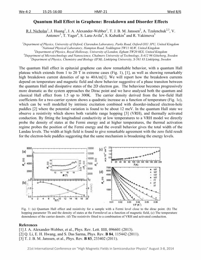
We-‐4-‐2 15:25-‐16:00 HMF-‐21 Wed 8/6
21st International Conference on "High Magnetic Fields in Semiconductor Physics" August 3-‐8, 2014
Quantum Hall Effect in Graphene: Breakdown and Disorder Effects
R.J. Nicholas1, J. Huang1, J. A. Alexander-Webber1, T. J. B. M. Janssen2, A. Tzalenchuk2,3, V. Antonov3, T. Yager4, S. Lara-Avila4, S. Kubatkin4 and R. Yakimova5
1Department of Physics, University of Oxford, Clarendon Laboratory, Parks Road, Oxford OX1 3PU, United Kingdom
2National Physical Laboratory, Hampton Road, Teddington TW11 0LW, United Kingdom 3Department of Physics, Royal Holloway, University of London, Egham TW20 0EX, United Kingdom
4Department of Microtechnology and Nanoscience, Chalmers University of Technology, S-412 96 Göteborg, Sweden 5Department of Physics, Chemistry and Biology (IFM), Linköping University, S-581 83 Linköping, Sweden
The quantum Hall effect in epitaxial graphene can show remarkable behavior, with a quantum Hall plateau which extends from 1 to 20 T in extreme cases (Fig. 1), [1], as well as showing remarkably high breakdown current densities of up to 40A/m[1]. We will report how the breakdown currents depend on temperature and magnetic field and show behavior suggestive of a phase transiton between the quantum Hall and dissipative states of the 2D electron gas. The behaviour becomes progressively more dramatic as the system approaches the Dirac point and we have analysed both the quantum and classical Hall effect from 1.5 up to 300K. The carrier density derived from the low-field Hall coefficients for a two-carrier system shows a quadratic increase as a function of temperature (Fig. 1c), which can be well modelled by intrinsic excitation combined with disorder-induced electron-hole puddles [2] where the potential variation is found to be about 12 meV. In the quantum Hall state we observe a resistivity which shows both variable range hopping [3] (VRH), and thermally activated conduction. By fitting the longitudinal conductivity at low temperatures to a VRH model we directly probe the density of states at the Fermi energy and at higher temperatures, the thermal activation regime probes the position of the Fermi energy and the overall behavior gives the total width of the Landau levels. The width at high field is found to give remarkable agreement with the zero field result for the electron-hole puddles suggesting that the same mechanism is broadening the energy levels.
References [1] J. A. Alexander-Webber, et al., Phys. Rev. Lett. 111, 096601 (2013). [2] Q. Li, E. H. Hwang, and S. Das Sarma, Phys. Rev. B 84, 115442 (2011). [3] T. J. B. M. Janssen, et al., Phys. Rev. B 83, 233402 (2011).
Fig. 1: (a) Quantum Hall effect and resistivity for a sample with a Fermi level close to the dirac point. (b) The hopping parameter Th and the density of states at the Fermilevel as a function of magnetic field, (c) The temperature dependence of the carrier density. (d) The resistivity fitted to a combination of VRH and activated conduction.
We-‐5-‐1 18:50-‐19:15 HMF-‐21 Wed 8/6
21st International Conference on "High Magnetic Fields in Semiconductor Physics" August 3-‐8, 2014
High-Field Magnet Projects at the NHMFL
Mark Bird
National High Magnetic Field Laboratory, Tallahassee, FL, USA
Th-‐1-‐1 9:00-‐9:35 HMF-‐21 Thu 8/7
21st International Conference on "High Magnetic Fields in Semiconductor Physics" August 3-‐8, 2014
Resistively-detected Nuclear Resonance in Quantum Hall Systems
Yoshiro Hirayama(1),(2),(3)
1Department of Physics, Tohoku University, Sendai 980-8578, Japan 2JST-ERATO Nuclear Spin Electronics Project, Sendai 980-8578i, Japan
3WPI-AIMR, Tohoku University, Sendai 980-8577, Japan
Dynamic nuclear polarization and resistive detection of nuclear polarization open us highly-sensitive resistively-detected NMR (nuclear magnetic resonance) in quantum-Hall systems. The pump and probe T1 time and NMR spectrum measurements clarify many interesting characteristics of electron spins confined in two-dimensions.
Nuclear spins can be dynamically polarized in GaAs quantum well by using several different methods. The spin phase transition (SPT) characteristics at ν = 2/3 allows us to detect such nuclear polarization. Nuclear polarization at very low temperature or induced by circularly polarized optical illumination results in spatially uniform nuclear polarization. On the other hand, large current flow at ν = 2/3 SPT results in spatially inhomogeneous nuclear polarization reflecting domain structures formed at SPT. Although inhomogeneity complicates experimental results, this inhomogeneity helps us to understand some physics. The selective nuclear polarization in one of the bilayer quantum wells based on ν = 2/3 SPT enables us to study nuclear diffusion both parallel and perpendicular to the quantum well. We found a strong suppression of nuclear diffusion in the perpendicular direction through the barrier. Interesting phenomenon appears when we expose the nuclear system polarized dynamically at ν = 2/3 SPT to the bilayer canted spin state with strong Goldstone mode at total filling factor 2. Sudden change in nuclear polarization distribution occurs by one second exposure in addition to extremely rapid nuclear relaxation. This suggests novel corrective phenomena including both electron and nuclear spins.
Finally, I briefly discuss nuclear manipulation mediated by oscillating electric field. The nuclear resonance can be induced by electron density oscillation caused by oscillatory gate voltage. This type of nuclear manipulation can be applied to a local control of nuclear spins by using nanoscale scanning gate, resulting in microscopic MRI (magnetic resonance image) in quantum Hall systems.

Th-‐1-‐2 9:35-‐9:55 HMF-‐21 Thu 8/7
21st International Conference on "High Magnetic Fields in Semiconductor Physics" August 3-‐8, 2014
NMR Probing of the Electronic Ground States in the Vicinity of the ν = 1 Quantum Hall State
W. Desrat (1, 2)*, B.A. Piot (1)*, S. Krämer (1), D. K. Maude (1), Z. R. Wasilewski (3), M. Henini (4), R.
Airey (5)
1Laboratoire National des Champs Magnétiques Intenses, CNRS-UJF-UPS-INSA, F-38042 Grenoble, France 2Laboratoire Charles Coulomb UMR 5221, Université Montpellier 2 and CNRS, F-34095 Montpellier, France
3Department of Electrical and Computer Engineering, University of Waterloo, Waterloo, Ontario, Canada 4School of Physics and Astronomy, University of Nottingham, Nottingham NG7 2RD, United Kingdom
5Department of Electronic and Electrical Engineering, University of Sheffield, Sheffield S1 4DU, United Kingdom
Resistively detected nuclear magnetic resonance (RDNMR) is a well-established technique to probe the interaction between nuclear and electronic spin systems via the contact hyperfine interaction. It has proved to be a formidable tool to investigate quantum Hall (QH) physics, enabling us to evidence peculiar spin textures such as skyrmions, or to measure the spin polarization of fractional and integer QH states. In particular, much attention has been focused on the RDNMR response around the filling factor ν = 1 QH state, following the observation of an unexpected dispersive line shape (DLS) (see figure 1.a), which origin has so far remained elusive. In our work, we present a systematic study of the RDNMR response in the vicinity of the ν ~ 1 QH state as a function of filling factor, carrier density, and nuclear isotope.
The frequency splitting between the dip and the peak of the DLS increases as the filling factor tends to ν = 1 (see figure 1.b), similar to the usual Knight shift versus ν dependence which reflects the depolarization of the electron system due to the formation of Skyrmions away from the exact ν = 1 filling factor [1]. The splitting is also proportional to the electron density and the gyromagnetic ratio of the nuclear isotope probed, as is the hyperfine coupling at the origin of the Knight shift. The peak frequency shifts linearly with magnetic field throughout the studied filling factor range and matches the unshifted substrate signal, detected by a classical (inductive) NMR experiment performed simultaneously. Thus, the evolution of the splitting is entirely due to the changing Knight shift of the dip feature (see Figure 1.b). The nuclear spin relaxation time T1
at precisely the peak frequency is extremely long (∼ hours). These results are consistent with the local formation of a ν = 2 phase due to the existence of spin singlet D- complexes in the 2D system. The anomalous RDNMR response of the ν = 1 QH state is thus a manifestation of the coexistence of two electron subsystems bearing different spin polarization [2]. * W.D. and B.A.P contributed equally to this work
References [1] S. E. Barrett et al, Phys. Rev. Lett. 74, 5112 (1995). [2] W. Desrat et al, Phys. Rev. B. 88, 241306 (R) (2013).
Fig. 1: (a) Dispersive RDNMR lineshape in the vicinity of the ν = 1 QH state. (b) Evolution of the peak and dip frequencies of the lineshape around ν = 1. The origin of the scale is taken at the average peak position and coincides with the position of the (unshifted) NMR of the GaAs substrate nuclei.

Th-‐1-‐3 9:55-‐10:15 HMF-‐21 Thu 8/7
21st International Conference on "High Magnetic Fields in Semiconductor Physics" August 3-‐8, 2014
Probing Charge Order in the N = 2 Landau Level Using NMR
Trevor D. Rhone (1,2), Koji Muraki (1,2)
1 NTT Basic Research Laboratories, NTT Corporation, Atsugi, Japan 2ERATO Nuclear Spin Electronics Project, Japan Science and Technology Agency (JST)
We probe the charge order of a two-dimensional electron system (2DES), confined to a GaAs quantum well, in the filling factor range 4.0 ≤ v ≤ 4.5 using resistively detected nuclear magnetic resonance (RD-NMR) spectroscopy at milliKelvin temperatures. It is well known that electron charge density waves, comprising stripe phases, bubble phases and Wigner crystals, characterize the 2DES in the higher Landau levels (N ≥ 2 LL). However few experiments have examined the internal structure of these phases. We use RD-NMR as a novel probe of the charge order of these exotic forms of matter. We report striking anomalies in the RD-NMR spectral line shape which we find arises due to translational symmetry breaking in the 2DES. Comparing experimental RD-NMR spectra with numerical simulations allows us to characterize the underlying electron density fluctuations which give rise to spectral anomalies, thereby elucidating the internal structure of the 2DES. For the stripe phase, at elevated temperatures, where transport is isotropic, RD-NMR reveals the persistence of local charge inhomogeneity in the 2DES. This suggests the possibility to probe short range charge order of stripe phases in the absence of long range orientational order.

Th-‐1-‐4 10:15-‐10:35 HMF-‐21 Thu 8/7
21st International Conference on "High Magnetic Fields in Semiconductor Physics" August 3-‐8, 2014
Coherent Larmor Precession of a Single Mn2+ Spin
M. Koperski (1,2), M. Goryca (1), P. Wojnar (3), T. Smoleński (1), A. Golnik (1), P. Kossacki (1)
1Institute of Experimental Physics, Faculty of Physics, University of Warsaw, Warsaw, Poland 2Grenoble High Magnetic Field Laboratory, CNRS, Grenoble, France
3Institute of Physics, Polish Academy of Sciences, Warsaw, Poland
Optical studies of CdTe/ZnTe quantum dots with a single Mn2+ ion revealed a large number of possible ways of spin manipulation with light. For example, a proper excitation of the system leads to the orientation of the spin of the Mn2+ ion, which may be utilized as a single spin memory with the life time in the microsecond range [1,2]. However, a complete control of the single spin requires the ability to coherently address particular quantum states of the magnetic ion. Here, we present the first observation of the spontaneous coherent oscillations of a single magnetic dopant in a quantum dot. In order to initialize and monitor a specific state of the spin of the Mn2+ ion, we use a system of coupled pair of quantum dots with a single magnetic dopant in one of them. By tuning the laser energy with the excitonic state in one quantum dot one can observe enhanced emission from the second dot as a result of the fast transfer of the exciton between the dots. The presence of the Mn2+ ion in the absorbing dot leads to the characteristic sixfold splitting of the resonance in the photoluminescence excitation spectrum (figure 1a). Each of the six lines corresponds to one of the six possible projections of the Mn2+ spin on the quantization axis. We place the system in the external magnetic field in Voigt configuration and excite it with pairs of picosecond laser pulses with controllable delay between them. The laser energy is tuned to one of the six resonances. In such a case the absorption of the first pulse causes a depletion of a specific state of the Mn2+ ion (+5/2 for instance). The photocreated exciton transfers into the neighboring dot within a few picoseconds. The initiated state of the Mn2+ spin starts to precess around the axis defined by the magnetic field leading to the modulation of the absorption for the second pulse. Therefore, the observed oscillations of the emission intensity from the non-magnetic dot, as shown in figure 1b, reflect the coherent Larmor precession of the Mn2+ spin in the absorbing dot. In the presentation we will analyze the main factors that determine the decoherence time T2
*, which was found to be about 0.5 ns. We will discuss the possible implications of our finding on the growing field of physics of quantum dots with single magnetic ions, taking into account different host semiconductor materials and various types of magnetic ions.
References [1] M. Goryca, et al., Phys. Rev. Lett. 103, 087401 (2009) [2] C. Le Gall, et al., Phys. Rev. Lett. 102, 127402 (2009) [3] M. Koperski, et al., Phys. Rev. B 89, 075311 (2014)
Fig. 1: (a) The photoluminescence excitation measurement enables the identification of a pair of coupled quantum dots with a single Mn2+ ion by the characteristic sixfold splitting of the resonance. (b) Time resolved experiments reveal the coherent precession of the single Mn2+ spin in a magnetic field.

Th-‐2-‐1 11:00-‐11:20 HMF-‐21 Thu 8/7
21st International Conference on "High Magnetic Fields in Semiconductor Physics" August 3-‐8, 2014
Spin-dependent Transport, Relaxation, and Nuclear Polarization in Si:P and Silicon-based Devices Studied by High-field Electrically-detected Magnetic
Resonance
J. van Tol(1), C.C. Lo(2,*), C.D. Weis(2), T. Schenkel(2), D.R. McCamey(3,#), G.W. Morley(4,&), C. Boehme(5)
1National High Magnetic Field Lab / Florida State University, Tallahassee, FL 32210, USA
2Accelerator and Fusion Research Division, Lawrence Berkeley National Lab, Berkeley, CA 94720, USA 3Department of Physics, University of Utah, 115 South 1400 East, Salt Lake City, Utah 84112, USA
4London Centre for Nanotechnology, University College London, London WC1H 0AH, United Kingdom 3School of Physics, University of Sydney, Sydney, New South Wales 2006, Australia
*Present address: London Centre for Nanotechnology, University College London, London WC1H 0AH, United Kingdom
# Present address, School of Physics, University of New South Wales, Sydney, NSW 2052, Australia &Present address: Department of Physics, University of Warwick, Coventry CV4 7AL, UK.
Nuclear and electron spins can be used to store and process information, and have been proposed as the basic building blocks for quantum information processing. They can be manipulated by magnetic fields and resonant radiation pulses. Impurities in silicon appear particularly attractive for this purpose, as relaxation times can be extremely long, and silicon technology is advanced.
High-fields and frequencies allow a high resolution and, at low temperatures, an almost complete electron spin polarization which can be transferred to the nuclear spins[1]. Electrical detection enables the detection of small spin ensembles, and a combination of pulsed Electron and Nuclear magnetic resonance techniques allow the determination of the both the electron and nuclear spin-lattice relaxation (T1)[1] and coherence times (T2)[2]. While in low-doping silicon charge carriers have to be created by light illumination, silicon field effect transistors allow operation without any radiation. Now the 2D electron gas below the gate interacts with phosphorus impurities in the silicon. By measuring the nuclear spin polarization directly from the intensity of the 31P hyperfine components of the EPR spectrum measured in the source-drain current, it can be
shown that the nuclear spins can be positive or negatively polarized depending on gate voltage and filling factor in the quantum Hall regime[3], using only DC electric fields and currents. This work was supported by the NSF (NHMFL), ARC (D.R.M.), EPSRC (G.W.M), DOE (LBNL), and NSA (LBNL) References [1] D.R. McCamey, J. van Tol, G.W. Morley, C. Boehme, Science 330, 1652-1656 (2010) [2] D.R. McCamey, G.W. Morley, C. Boehme, and J. van Tol, Phys. Rev. B. 85, 073201 (2012) [3] C.C. Lo, C.D. Weis, J. van Tol, J. Bokor, and T. Schenkel, Phys. Rev. Lett. 110 , 057601 (2013)
Fig. 1: Current response in a typical electron-nuclear pulse sequence in an electrically-detected nuclear T2 experiment in Si:P. Current responses to RF pulses are spurious, the response to millimeter waves (mmw) reflects the spin dependent transport signal.
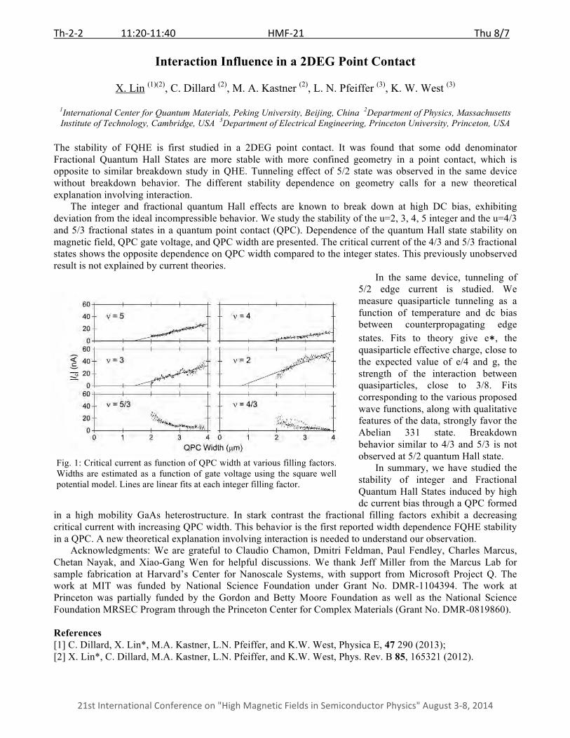
Th-‐2-‐2 11:20-‐11:40 HMF-‐21 Thu 8/7
21st International Conference on "High Magnetic Fields in Semiconductor Physics" August 3-‐8, 2014
Interaction Influence in a 2DEG Point Contact
X. Lin (1)(2), C. Dillard (2), M. A. Kastner (2), L. N. Pfeiffer (3), K. W. West (3)
1International Center for Quantum Materials, Peking University, Beijing, China 2Department of Physics, Massachusetts Institute of Technology, Cambridge, USA 3Department of Electrical Engineering, Princeton University, Princeton, USA
The stability of FQHE is first studied in a 2DEG point contact. It was found that some odd denominator Fractional Quantum Hall States are more stable with more confined geometry in a point contact, which is opposite to similar breakdown study in QHE. Tunneling effect of 5/2 state was observed in the same device without breakdown behavior. The different stability dependence on geometry calls for a new theoretical explanation involving interaction. The integer and fractional quantum Hall effects are known to break down at high DC bias, exhibiting deviation from the ideal incompressible behavior. We study the stability of the u=2, 3, 4, 5 integer and the u=4/3 and 5/3 fractional states in a quantum point contact (QPC). Dependence of the quantum Hall state stability on magnetic field, QPC gate voltage, and QPC width are presented. The critical current of the 4/3 and 5/3 fractional states shows the opposite dependence on QPC width compared to the integer states. This previously unobserved result is not explained by current theories.
In the same device, tunneling of 5/2 edge current is studied. We measure quasiparticle tunneling as a function of temperature and dc bias between counterpropagating edge states. Fits to theory give e∗, the quasiparticle effective charge, close to the expected value of e/4 and g, the strength of the interaction between quasiparticles, close to 3/8. Fits corresponding to the various proposed wave functions, along with qualitative features of the data, strongly favor the Abelian 331 state. Breakdown behavior similar to 4/3 and 5/3 is not observed at 5/2 quantum Hall state. In summary, we have studied the stability of integer and Fractional Quantum Hall States induced by high dc current bias through a QPC formed
in a high mobility GaAs heterostructure. In stark contrast the fractional filling factors exhibit a decreasing critical current with increasing QPC width. This behavior is the first reported width dependence FQHE stability in a QPC. A new theoretical explanation involving interaction is needed to understand our observation. Acknowledgments: We are grateful to Claudio Chamon, Dmitri Feldman, Paul Fendley, Charles Marcus, Chetan Nayak, and Xiao-Gang Wen for helpful discussions. We thank Jeff Miller from the Marcus Lab for sample fabrication at Harvard’s Center for Nanoscale Systems, with support from Microsoft Project Q. The work at MIT was funded by National Science Foundation under Grant No. DMR-1104394. The work at Princeton was partially funded by the Gordon and Betty Moore Foundation as well as the National Science Foundation MRSEC Program through the Princeton Center for Complex Materials (Grant No. DMR-0819860).
References [1] C. Dillard, X. Lin*, M.A. Kastner, L.N. Pfeiffer, and K.W. West, Physica E, 47 290 (2013); [2] X. Lin*, C. Dillard, M.A. Kastner, L.N. Pfeiffer, and K.W. West, Phys. Rev. B 85, 165321 (2012).
Fig. 1: Critical current as function of QPC width at various filling factors. Widths are estimated as a function of gate voltage using the square well potential model. Lines are linear fits at each integer filling factor.
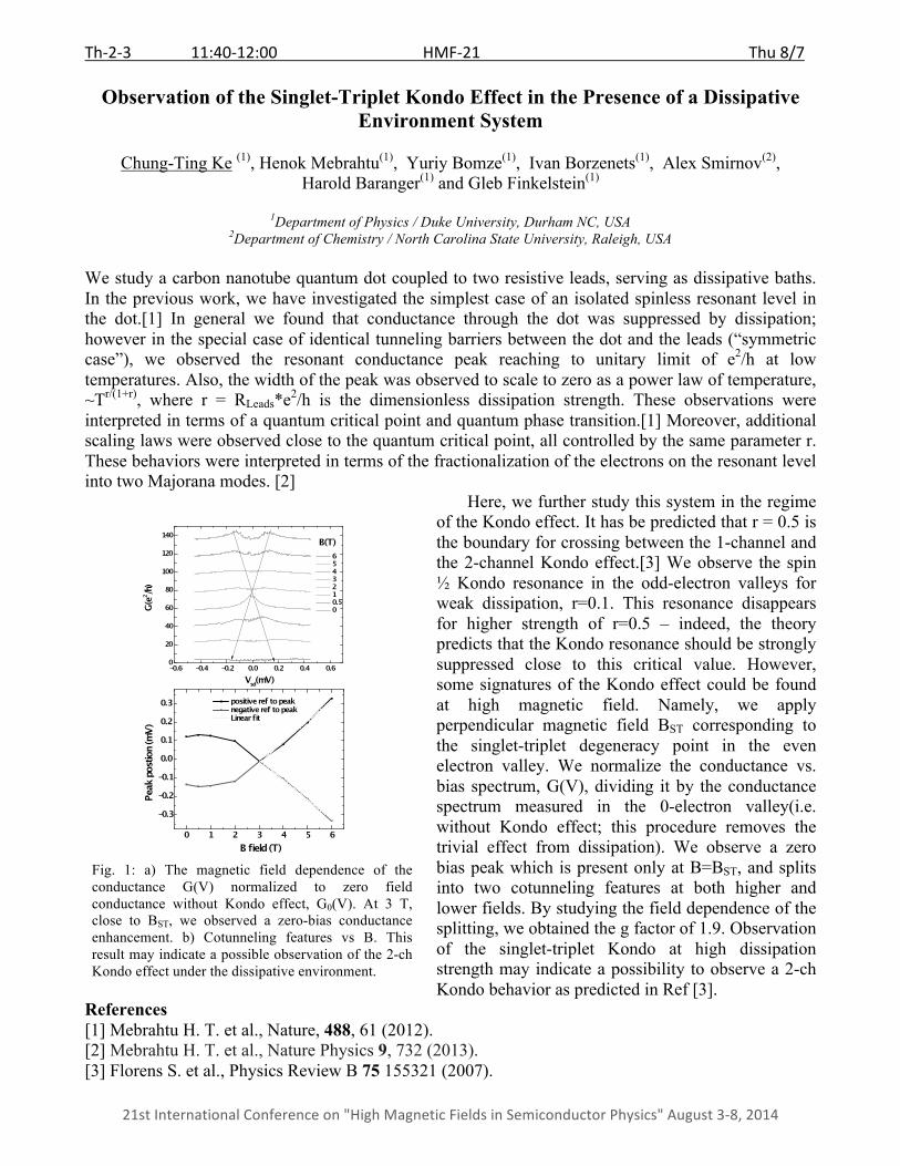
Th-‐2-‐3 11:40-‐12:00 HMF-‐21 Thu 8/7
21st International Conference on "High Magnetic Fields in Semiconductor Physics" August 3-‐8, 2014
Observation of the Singlet-Triplet Kondo Effect in the Presence of a Dissipative Environment System
Chung-Ting Ke (1), Henok Mebrahtu(1), Yuriy Bomze(1), Ivan Borzenets(1), Alex Smirnov(2),
Harold Baranger(1) and Gleb Finkelstein(1)
1Department of Physics / Duke University, Durham NC, USA 2Department of Chemistry / North Carolina State University, Raleigh, USA
We study a carbon nanotube quantum dot coupled to two resistive leads, serving as dissipative baths. In the previous work, we have investigated the simplest case of an isolated spinless resonant level in the dot.[1] In general we found that conductance through the dot was suppressed by dissipation; however in the special case of identical tunneling barriers between the dot and the leads (“symmetric case”), we observed the resonant conductance peak reaching to unitary limit of e2/h at low temperatures. Also, the width of the peak was observed to scale to zero as a power law of temperature, ~Tr/(1+r), where r = RLeads*e2/h is the dimensionless dissipation strength. These observations were interpreted in terms of a quantum critical point and quantum phase transition.[1] Moreover, additional scaling laws were observed close to the quantum critical point, all controlled by the same parameter r. These behaviors were interpreted in terms of the fractionalization of the electrons on the resonant level into two Majorana modes. [2]
Here, we further study this system in the regime of the Kondo effect. It has be predicted that r = 0.5 is the boundary for crossing between the 1-channel and the 2-channel Kondo effect.[3] We observe the spin ½ Kondo resonance in the odd-electron valleys for weak dissipation, r=0.1. This resonance disappears for higher strength of r=0.5 – indeed, the theory predicts that the Kondo resonance should be strongly suppressed close to this critical value. However, some signatures of the Kondo effect could be found at high magnetic field. Namely, we apply perpendicular magnetic field BST corresponding to the singlet-triplet degeneracy point in the even electron valley. We normalize the conductance vs. bias spectrum, G(V), dividing it by the conductance spectrum measured in the 0-electron valley(i.e. without Kondo effect; this procedure removes the trivial effect from dissipation). We observe a zero bias peak which is present only at B=BST, and splits into two cotunneling features at both higher and lower fields. By studying the field dependence of the splitting, we obtained the g factor of 1.9. Observation of the singlet-triplet Kondo at high dissipation strength may indicate a possibility to observe a 2-ch Kondo behavior as predicted in Ref [3].
References [1] Mebrahtu H. T. et al., Nature, 488, 61 (2012). [2] Mebrahtu H. T. et al., Nature Physics 9, 732 (2013). [3] Florens S. et al., Physics Review B 75 155321 (2007).
Fig. 1: a) The magnetic field dependence of the conductance G(V) normalized to zero field conductance without Kondo effect, G0(V). At 3 T, close to BST, we observed a zero-bias conductance enhancement. b) Cotunneling features vs B. This result may indicate a possible observation of the 2-ch Kondo effect under the dissipative environment.

Th-‐2-‐4 12:00-‐12:20 HMF-‐21 Thu 8/7
21st International Conference on "High Magnetic Fields in Semiconductor Physics" August 3-‐8, 2014
Novel Method to Quantify Density Gradients in 2D Samples
W. Zhou (1), H. M. Yoo (1), S. Prabhu-Gaunkar (1), L. Tiemann (2), C. Reichl (2), W. Wegscheider (2), and M. Grayson (1)
1Department of Electrical Engineering and Computer Science, Northwestern University, Evanston, IL 60208, USA
2Laboratory for Solid State Physics, ETH Zurich, 8093 Zurich, Switzerland
We demonstrate an experimental method to quantify arbitrarily oriented density gradients in rectangular van der Pauw (vdP) samples, by characterizing the asymmetric longitudinal resistance (ALR) observed at positive and negative fields. Measuring the two longitudinal vdP resistances along two perpendicular directions Rxx and Ryy at both positive and negative magnetic fields (+B and –B), the density gradient is deduced as follows from a conformally mapped current stream function:
n0 = mean density, ρ0 = mean resistivity L = sample side length Rxx , Ryy = longitudinal resistances
Unlike prior experimental work by Pan et al. [1] and theoretical work by Ilan et al. [2] which considered unquantified large density gradients at right angles to the sample sides, the density gradients considered here can be quantified for arbitrary orientation.
The ALR analysis is verified on square samples cleaved from a high-mobility quantum well (QW) wafer grown without rotation in a molecular beam epitaxy (MBE) chamber. The density distribution map (Fig. 1) is first measured from the local density of several dozen cleaved samples, and the density gradients (black arrows) are deduced from these values. The ALR analysis is then tested by comparing to these gradients: green (pink) arrows use the four corner (flat) contacts of the vdP samples, respectively. The agreement of the arrows at various locations of the sample to within ∇n = ±0.05×1011 cm-2/cm verifies the accuracy of our method. The ALR analysis is expected to aid in improving the uniformity of epitaxially grown high-mobility QW wafers as well as improving the interpretation of Hall effect data in the presence of density gradients. We demonstrate that in very high mobility samples such as where this effect was first discovered (Pan et al. [1]) the exact
angle of the density gradient can still be determined with high accuracy from the ALR analysis even if the magnitude of the density gradient is difficult to determine. The authors would like to thank Professor Dominik Zumbuhl at University of Basel for helpful discussions.
References [1] W. Pan et al., Phys. Rev. Lett. 95, 066808 (2005). [2] R. Ilan, N. R. Cooper, and A. Stern, Phys. Rev. B 73, 235333 (2006).
Fig. 1: Density color map of 2-inch GaAs QW wafer calibrated from dicing it into 4×4 mm2 samples. Black arrows represent density gradients from the local density map, and the green (pink) arrows represent the density gradients using the ALR analysis method introduced here using corner (flat) contacts.
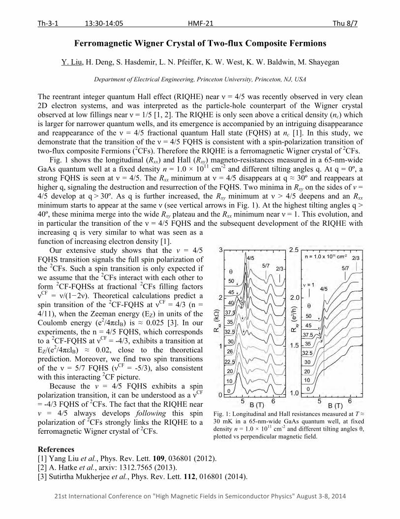
Th-‐3-‐1 13:30-‐14:05 HMF-‐21 Thu 8/7
21st International Conference on "High Magnetic Fields in Semiconductor Physics" August 3-‐8, 2014
Ferromagnetic Wigner Crystal of Two-flux Composite Fermions
Y. Liu, H. Deng, S. Hasdemir, L. N. Pfeiffer, K. W. West, K. W. Baldwin, M. Shayegan
Department of Electrical Engineering, Princeton University, Princeton, NJ, USA
The reentrant integer quantum Hall effect (RIQHE) near ν = 4/5 was recently observed in very clean 2D electron systems, and was interpreted as the particle-hole counterpart of the Wigner crystal observed at low fillings near ν = 1/5 [1, 2]. The RIQHE is only seen above a critical density (nc) which is larger for narrower quantum wells, and its emergence is accompanied by an intriguing disappearance and reappearance of the ν = 4/5 fractional quantum Hall state (FQHS) at nc [1]. In this study, we demonstrate that the transition of the ν = 4/5 FQHS is consistent with a spin-polarization transition of two-flux composite Fermions (2CFs). Therefore the RIQHE is a ferromagnetic Wigner crystal of 2CFs. Fig. 1 shows the longitudinal (Rxx) and Hall (Rxy) magneto-resistances measured in a 65-nm-wide GaAs quantum well at a fixed density n = 1.0 × 1011 cm-2 and different tilting angles q. At q = 0º, a strong FQHS is seen at ν = 4/5. The Rxx minimum at ν = 4/5 disappears at q ≈ 30º and reappears at higher q, signaling the destruction and resurrection of the FQHS. Two minima in Rxy on the sides of ν = 4/5 develop at q > 30º. As q is further increased, the Rxy minimum at ν > 4/5 deepens and an Rxx minimum starts to appear at the same ν (see vertical arrows in Fig. 1). At the highest tilting angles q > 40º, these minima merge into the wide Rxy plateau and the Rxx minimum near ν = 1. This evolution, and in particular the transition of the ν = 4/5 FQHS and the subsequent development of the RIQHE with increasing q is very similar to what was seen as a function of increasing electron density [1]. Our extensive study shows that the ν = 4/5 FQHS transition signals the full spin polarization of the 2CFs. Such a spin transition is only expected if we assume that the 2CFs interact with each other to form 2CF-FQHSs at fractional 2CFs filling factors νCF = ν/(1−2ν). Theoretical calculations predict a spin transition of the 2CF-FQHS at νCF = 4/3 (n = 4/11), when the Zeeman energy (EZ) in units of the Coulomb energy (e2/4πεlB) is ≈ 0.025 [3]. In our experiments, the n = 4/5 FQHS, which corresponds to a 2CF-FQHS at νCF = -4/3, exhibits a transition at EZ/(e2/4πεlB) ≈ 0.02, close to the theoretical prediction. Moreover, we find two spin transitions of the ν = 5/7 FQHS (νCF = -5/3), also consistent with this interacting 2CF picture. Because the ν = 4/5 FQHS exhibits a spin polarization transition, it can be understood as a νCF = -4/3 FQHS of 2CFs. The fact that the RIQHE near ν = 4/5 always develops following this spin polarization of 2CFs strongly links the RIQHE to a ferromagnetic Wigner crystal of 2CFs.
References [1] Yang Liu et al., Phys. Rev. Lett. 109, 036801 (2012). [2] A. Hatke et al., arxiv: 1312.7565 (2013). [3] Sutirtha Mukherjee et al., Phys. Rev. Lett. 112, 016801 (2014).
Fig. 1: Longitudinal and Hall resistances measured at T ≈ 30 mK in a 65-nm-wide GaAs quantum well, at fixed density n = 1.0 × 1011 cm-2 and different tilting angles θ, plotted vs perpendicular magnetic field.

Th-‐3-‐2 14:05-‐14:25 HMF-‐21 Thu 8/7
21st International Conference on "High Magnetic Fields in Semiconductor Physics" August 3-‐8, 2014
Microwave Spectroscopic Observation of a Bilayer Inter-solid Transition in a Wide Single Quantum Well
A. T. Hatke (1), Y. Liu (2), L. W. Engel (1), M. Shayegan (2), L. N. Pfeiffer (2), K. W. West (2), K. W.
Baldwin (2)
1National High Magnetic Field Laboratory, Tallahassee, Florida, USA
2Department of Electrical Engineering, Princeton University, Princeton, New Jersey, USA
Electrons in wide quantum wells (WQWs) can be tuned from forming a thick single layer to forming a system of two parallel single layers by increasing the carrier density, n. At intermediate n, interlayer and intralayer interactions are comparable, producing interlayer correlated states such as the fractional quantum Hall effect (FQHE) at Landau filling factor ν=1/2 [1]. Transport measurements [2] on WQWS at the low n termination of the FQHE series have revealed an insulating phase (IP), which was interpreted as an electron solid related to the Wigner crystal. As n is increased [2] and the electrons distribute themselves in two layers, producing an increase in the n below which the IP appears. The IP can be reentrant on the high ν side of the ½ FQHE.
Fig. 1: Color image of the real part of the diagonal conductivity in the f-ν plane at three different n in units of 1011 cm-2. Microwave spectroscopy is a prime measurement technique for investigating electron solids due to the pinning mode resonance, a signature of a solid. Here we have investigated the microwave response of an 80 nm WQW for ν < 0.55. Figure 1 shows color maps in the f-ν plane of the real part of the diagonal conductivity at different n. For these measurements we have maintained an approximate symmetry of the charge distribution about the center of the well. In Fig. 1a, n = 1.19×1011 cm-2, a resonance occurs for ν below 0.33. In Fig. 1b and c, n = 1.35 and 1.52×1011 cm-2, the onset of the resonance is at higher ν, and the 1/2 FQHE (no resonance) borders the solid, indicating interlayer correlations may play a role in the adjacent solid. In Fig. 1b, but not c, there is an abrupt shift in the pinning mode within the IP near ν ~ 0.37. This shift is interpreted as a transition between competing bilayer phases. Multiple phases of bilayer electron solids have been studied in variational approximations [3], though for an 80 nm WQW at ν~0.4, all the predicted transitions would occur at n at least several times that in Fig.1b. Correlations that are not incorporated into the theories are a possible explanation of the discrepancy. References [1] Y.W. Suen et al., PRL 68, 1379 (1992); J.P. Eisenstein et al., ibid. 1383. [2] H.C. Manoharan et al., PRL 77, 1813 (1996). [3] L. Zheng and H.A. Fertig, PRB 52, 12282 (1995); S. Narasimhan and T.L. Ho, ibid. 12291.
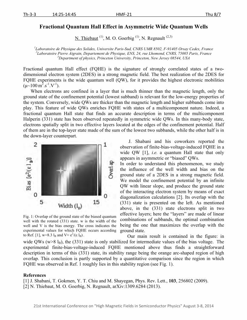
Th-‐3-‐3 14:25-‐14:45 HMF-‐21 Thu 8/7
21st International Conference on "High Magnetic Fields in Semiconductor Physics" August 3-‐8, 2014
Fractional Quantum Hall Effect in Asymmetric Wide Quantum Wells
N. Thiebaut (1), M. O. Goerbig (1), N. Regnault (2,3)
1Laboratoire de Physique des Solides, Universite Paris-Sud, CNRS UMR 8502, F-91405 Orsay Cedex, France
2Laboratoire Pierre Aigrain, Departement de Physique, ENS, 24, rue Lhomond, CNRS, 75005 Paris, France
3Department of physics, Princeton University, Princeton, New Jersey 08544, USA
Fractional quantum Hall effect (FQHE) is the signature of strongly correlated states of a two-dimensional electron system (2DES) in a strong magnetic field. The best realization of the 2DES for FQHE experiments is the wide quantum well (QW), for it provides the highest electronic mobilities (µ~100 m2.s-1.V-1). When electrons are confined in a layer that is much thinner than the magnetic length, only the ground state of the confinement potential (lowest subband) is relevant for the low-energy properties of the system. Conversely, wide QWs are thicker than the magnetic length and higher subbands come into play. This feature of wide QWs enriches FQHE with states of a multicomponent nature. Indeed, a fractional quantum Hall state that finds an accurate description in terms of the multicomponent Halperin (331) state has been observed repeatedly in symmetric wide QWs. In this many-body state, electrons spatially split in two effective layers located at the edges of the confinement potential. Half of them are in the top-layer state made of the sum of the lowest two subbands, while the other half is in the down-layer counterpart.
J. Shabani and his coworkers reported the observation of finite-bias-voltage-induced FQHE in a wide QW [1], i.e. a quantum Hall state that only appears in asymmetric or “biased” QWs. In order to understand this phenomenon, we study the influence of the well width and bias on the ground state of a 2DES in a strong magnetic field. We model the confinement potential by an infinite QW with linear slope, and produce the ground state of the interacting electron system by means of exact diagonalization calculations [2]. Its overlap with the (331) state is presented on the left. As mentioned above, in the (331) state electrons split in two effective layers; here the “layers” are made of linear combinations of subbands, the optimal combination being the one that maximizes the overlap with the ground state. Our main result is contained in the figure: in
wide QWs (w>8 lB), the (331) state is only stabilized for intermediate values of the bias voltage. The experimental finite-bias-voltage-induced FQHE mentioned above thus finds a straightforward description in terms of this (331) state, its stability range being the orange arc-shaped region of high overlap. This conclusion is partly supported by a quantitative comparison since the region in which FQHE was observed in Ref. 1 roughly lies in this stability region (see Fig. 1). References [1] J. Shabani, T. Gokmen, Y. T. Chiu and M. Shayegan, Phys. Rev. Lett., 103, 256802 (2009). [2] N. Thiebaut, M. O. Goerbig, N. Regnault, arXiv:1309.6284 (2013).
Fig. 1: Overlap of the ground state of the biased quantum well with the rotated (331) state. w is the width of the well and V is the bias energy. The cross indicates the experimental values for which FQHE occurs according to Ref. [1], w=8.3 lB and V≈ e2/(ε lB) .
Th-‐3-‐4 14:45-‐15:05 HMF-‐21 Thu 8/7
21st International Conference on "High Magnetic Fields in Semiconductor Physics" August 3-‐8, 2014
Coulomb Drag and Tunneling at νT=1 in a Quantum Hall Bilayer
D. Nandi (1), T. Khaire (1), A.D.K. Finck (1), J.P. Eisenstein (1), L.N. Pfeiffer (2), K.W. West (2)
1 Institute for Quantum Information and Matter, California Institute of Technology, Pasadena, CA 91125, USA 2Department of Electrical Engineering, Princeton University, Princeton, New Jersey, NJ 08544, USA
Exciton condensation is realized in a quantum Hall bilayer at νT=1 when the total electron density in the two layers matches the Landau level degeneracy. Early evidence of this remarkable state of matter came in tunneling [1] and counterflow [2] experiments done in Hall bar devices. As the total electron density at νT=1 is reduced below a critical value, and interlayer correlations become comparable to intralayer correlations, several dramatic transport features emerge. A strong enhancement, reminiscent of the dc Josephson effect, is observed in the zero bias tunneling conductance [1]. At the same time, transport measurements done with oppositely directed currents in each layer found a vanishing Hall resistance [2], suggestive of the counterflow current being carried by interlayer electron-hole pairs, i.e. excitons. However, since these experiments were done in Hall bar devices, it remained unclear what the relative roles of edge and bulk transport were. Subsequent experiments done in the multiply-connected Corbino geometry [3, 4, 5] demonstrate that both tunneling and exciton transport occur throughout the bulk. As in all quantum Hall states, the bulk of the 2D system is opaque to charge transport. At νT=1 however, there is a condensate of charge neutral interlayer excitons. It is this condensate which enables both tunneling and counterflow to extend across the bulk of the system. In this talk, we describe experimental measurements [4, 5] which vividly illustrate the nearly lossless transport of excitons across the bulk of the νT=1 bilayer quantum Hall state in a Corbino geometry. We highlight the observation that bulk exciton transport can be induced, via Coulomb drag, even when there are no explicit electrical connections between the two 2D layers. At the same time, we find, consistent with earlier measurements [1, 2], that a small amount of dissipation accompanies exciton transport down to the lowest temperatures studied. References [1] I. B. Spielman, J. P. Eisenstein, L. N. Pfeiffer, & K. W. West, Physical Review Letters, 84, 5808 (2000). [2] M. Kellogg, J. P.Eisenstein, L. N. Pfeiffer, & K. W. West, Physical Review Letters, 93, 036801 (2004). [3] A.D.K. Finck, J.P. Eisenstein, L. N. Pfeiffer, & K. W. West, Physical Review Letters, 106, 236807 (2011). [4] D. Nandi, A. D. K. Finck, J. P. Eisenstein, L. N. Pfeiffer, & K. W. West, Nature, 488, 481(2012). [5] D. Nandi, T. Khaire, A. D. K. Finck, J. P. Eisenstein, L. N. Pfeiffer, & K. W. West, Physical Review B, 88, 165308 (2013).
Th-‐4-‐1 15:30-‐16:05 HMF-‐21 Thu 8/7
21st International Conference on "High Magnetic Fields in Semiconductor Physics" August 3-‐8, 2014
Quantum Oscillations in Kondo Insulator SmB6
Lu Li
University of Michigan, Ann Arbor, MI, U.S.A. In Kondo insulator samarium hexaboride SmB6, strong correlation and band hybridization lead to a diverging resistance at low temperature. The resistance divergence ends at about 3 Kelvin, a behavior recently demonstrated to arise from the surface conductance. However, questions remain whether and where a topological surface state exists. Quantum oscillations have not been observed to map the Fermi surface [1]. We solve the problem by resolving the Landau Level quantization and Fermi surface topology using torque magnetometry. The observed angular dependence of the Fermi surface cross section suggests two-dimensional surface states on the (101) and (100) plane. Furthermore, similar to the quantum Hall states for graphene, the tracking of the Landau Levels in the infinite magnetic field limit points to -1/2, the Berry phase contribution from the 2D Dirac electronic state. References [1] G. Li, Z. Xiang, F. Yu, T. Asaba, B. Lawson, P. Kai, C. Tinsman, A. Berkeley, S. Wolgast, Y. S. Eo, D. J. Kim, C. Kurdak, K. Sun, J. W. Allen, X. H. Chen, Y. Wang, Z. Fisk, and Lu Li. “Quantum Oscillations in Kondo Insulator SmB6”, arXiv:1306.5221 (2013). Science, in Press.
Th-‐4-‐2 16:05-‐16:25 HMF-‐21 Thu 8/7
21st International Conference on "High Magnetic Fields in Semiconductor Physics" August 3-‐8, 2014
Theory of Magnetoresistance of Surface States in SmB6
M. Dzero(1), V. Galitski(2), and M. Vavilov(3)
1Department of Physics, Kent State University, Kent, Ohio, 44242, USA 2Condensed Matter Theory Center and Department of Physics, University of Maryland, College Park, MD 20742, USA
3Department of Physics, University of Wisconsin, Madison, WI 53562, USA
Kondo insulators are relatively new materials in focus of search for realizations of topological insulators (TI). These materials exhibit some of the most important properties of TI [1]. One known example of a Kondo insulator is Samarium hexaboride. SmB6. ARPES measurements [2] and quantum magneto-oscillations [3] indicate on the existence of the Dirac-like dispersion of electronic states at SmB6 surfaces. Furthermore, a detailed analysis of the conductivity in SmB6 suggests that at low temperatures transport in Kondo insulator SmB6 is dominated by the surface conduction states [4]. When a magnetic field is applied perpendicular to the surface, the sign of the magnetoresistance is consistent with antilocalization [5]. In this talk, we first discuss the effective Hamiltonian for the surface electron states [6]. We then consider weak localization effects for these states in the presence of a generic disorder. In particular, we evaluate dependence of the antilocalization correction on interband scattering rates. Our goal is to determine the number of localization and antilocalization modes and to identify the corresponding decoherence rates for these modes. We also evaluate oscillations in the density of states, smooth part of magnetoresistance and Shubnikov—de Haas oscillations in semiclassically strong magnetic fields. We expect that independent measurements of the antilocalization and quantum magneto—oscillations may be used to better describe the structure of disorder scattering. We provide comparison of our theory with experimental data. References [1] M. Dzero, K. Sun, V. Galitski, and P. Coleman, Phys. Rev. Lett. 104, 106408 (2010). [2] J. Jiang, et al., Nature Communications 4, 3010 (2013). [3] G. Li, et al, arXiv:1306.5221 (2013). [4] D.J. Kim, S. Thomas, T. Grant, J. Botimer, Z. Fisk, Jing Xia, Scientific Reports 3, 3150 (2013). [5] S. Thomas, D. J. Kim, S. B. Chung, T. Grant, Z. Fisk, and J. Xia, arXiv:1307.4133 (2013). [6] V. Alexandrov, M. Dzero, and P. Coleman, Phys. Rev. Lett. 111, 226403 (2013).
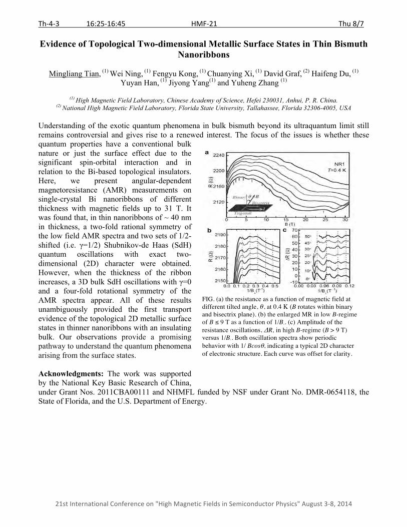
Th-‐4-‐3 16:25-‐16:45 HMF-‐21 Thu 8/7
21st International Conference on "High Magnetic Fields in Semiconductor Physics" August 3-‐8, 2014
Evidence of Topological Two-dimensional Metallic Surface States in Thin Bismuth Nanoribbons
Mingliang Tian, (1) Wei Ning, (1) Fengyu Kong, (1) Chuanying Xi, (1) David Graf, (2) Haifeng Du, (1)
Yuyan Han, (1) Jiyong Yang(1) and Yuheng Zhang (1)
(1) High Magnetic Field Laboratory, Chinese Academy of Science, Hefei 230031, Anhui, P. R. China.
(2) National High Magnetic Field Laboratory, Florida State University, Tallahassee, Florida 32306-4005, USA Understanding of the exotic quantum phenomena in bulk bismuth beyond its ultraquantum limit still remains controversial and gives rise to a renewed interest. The focus of the issues is whether these quantum properties have a conventional bulk nature or just the surface effect due to the significant spin-orbital interaction and in relation to the Bi-based topological insulators. Here, we present angular-dependent magnetoresistance (AMR) measurements on single-crystal Bi nanoribbons of different thickness with magnetic fields up to 31 T. It was found that, in thin nanoribbons of ~ 40 nm in thickness, a two-fold rational symmetry of the low field AMR spectra and two sets of 1/2-shifted (i.e. γ=1/2) Shubnikov-de Haas (SdH) quantum oscillations with exact two-dimensional (2D) character were obtained. However, when the thickness of the ribbon increases, a 3D bulk SdH oscillations with γ=0 and a four-fold rotational symmetry of the AMR spectra appear. All of these results unambiguously provided the first transport evidence of the topological 2D metallic surface states in thinner nanoribbons with an insulating bulk. Our observations provide a promising pathway to understand the quantum phenomena arising from the surface states. Acknowledgments: The work was supported by the National Key Basic Research of China, under Grant Nos. 2011CBA00111 and NHMFL funded by NSF under Grant No. DMR-0654118, the State of Florida, and the U.S. Department of Energy.
FIG. (a) the resistance as a function of magnetic field at different tilted angle, θ, at 0.4 K (B rotates within binary and bisectrix plane). (b) the enlarged MR in low B-regime of B ≤ 9 T as a function of 1/B⊥. (c) Amplitude of the resistance oscillations, ΔR, in high B-regime (B > 9 T) versus 1/B⊥. Both oscillation spectra show periodic behavior with 1/ Bcosθ, indicating a typical 2D character of electronic structure. Each curve was offset for clarity.
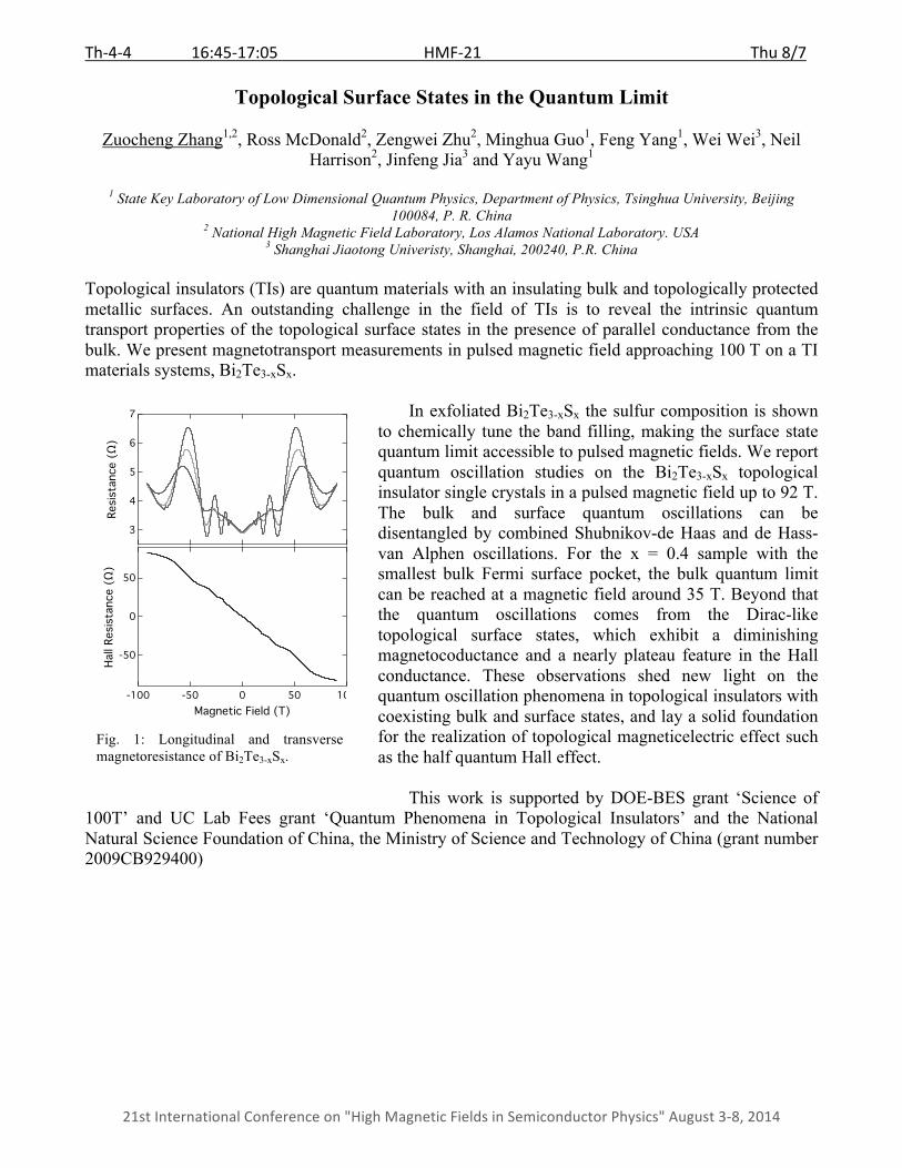
Th-‐4-‐4 16:45-‐17:05 HMF-‐21 Thu 8/7
21st International Conference on "High Magnetic Fields in Semiconductor Physics" August 3-‐8, 2014
Topological Surface States in the Quantum Limit
Zuocheng Zhang1,2, Ross McDonald2, Zengwei Zhu2, Minghua Guo1, Feng Yang1, Wei Wei3, Neil Harrison2, Jinfeng Jia3 and Yayu Wang1
1 State Key Laboratory of Low Dimensional Quantum Physics, Department of Physics, Tsinghua University, Beijing
100084, P. R. China 2 National High Magnetic Field Laboratory, Los Alamos National Laboratory. USA
3 Shanghai Jiaotong Univeristy, Shanghai, 200240, P.R. China
Topological insulators (TIs) are quantum materials with an insulating bulk and topologically protected metallic surfaces. An outstanding challenge in the field of TIs is to reveal the intrinsic quantum transport properties of the topological surface states in the presence of parallel conductance from the bulk. We present magnetotransport measurements in pulsed magnetic field approaching 100 T on a TI materials systems, Bi2Te3-xSx.
In exfoliated Bi2Te3-xSx the sulfur composition is shown to chemically tune the band filling, making the surface state quantum limit accessible to pulsed magnetic fields. We report quantum oscillation studies on the Bi2Te3-xSx topological insulator single crystals in a pulsed magnetic field up to 92 T. The bulk and surface quantum oscillations can be disentangled by combined Shubnikov-de Haas and de Hass-van Alphen oscillations. For the x = 0.4 sample with the smallest bulk Fermi surface pocket, the bulk quantum limit can be reached at a magnetic field around 35 T. Beyond that the quantum oscillations comes from the Dirac-like topological surface states, which exhibit a diminishing magnetocoductance and a nearly plateau feature in the Hall conductance. These observations shed new light on the quantum oscillation phenomena in topological insulators with coexisting bulk and surface states, and lay a solid foundation for the realization of topological magneticelectric effect such as the half quantum Hall effect. This work is supported by DOE-BES grant ‘Science of
100T’ and UC Lab Fees grant ‘Quantum Phenomena in Topological Insulators’ and the National Natural Science Foundation of China, the Ministry of Science and Technology of China (grant number 2009CB929400)
7
6
5
4
3
Resis
tanc
e (Ω
)
-50
0
50
Hall
Resis
tanc
e (Ω
)
-100 -50 0 50 100Magnetic Field (T)
Fig. 1: Longitudinal and transverse magnetoresistance of Bi2Te3-xSx.
Fr-‐1-‐1 9:00-‐9:35 HMF-‐21 Fri 8/8
21st International Conference on "High Magnetic Fields in Semiconductor Physics" August 3-‐8, 2014
Electric Dipole Moment Oscillations, Dark Excitons and THz Transitions in Aharonov-Bohm Quantum Rings
M. E. Portnoi
School of Physics, University of Exeter, Exeter, United Kingdom
Progress in epitaxial growth techniques has resulted in burgeoning developments in the physics of quantum dots – semiconductor-based “artificial atoms”. More recently a lot of attention has been turned towards non-simply-connected nanostructures, quantum rings, which have been obtained in various semiconductor systems [1-3]. The fascination in quantum rings is partially caused by a wide variety of purely quantum mechanical effects, which are observed in ring-like nanostructures. The star amongst them is the Aharonov-Bohm effect, in which a charged particle is influenced by a magnetic field away from the particle’s trajectory, resulting in magnetic-flux-dependent oscillations of the ring-confined particle energy. The oscillations of the single-particle energy are strongly suppressed by distortions of the ring shape or by applying an in-plane (lateral) electric field, thus reducing the symmetry of the system. However, there are other physical quantities, which might have even more pronounced magneto-oscillations when the symmetry of the ring is reduced. For example, in the presence of a lateral electric field exceeding a particular threshold it is possible to switch the ground state of an exciton in an Aharonov-Bohm ring from being optically active (bright) to optically inactive (dark) [4]. Another hitherto overlooked phenomenon is the flux-periodic change of an electric dipole moment of a quantum ring. We demonstrate that an external electric field applied in the ring plane results in strong oscillations of the electric-field-induced dipole moment with pronounced maxima when the flux piercing the ring is equal to an odd number of one half of the flux quantum [5]. These oscillations are accompanied by periodic changes in the selection rules for inter-level optical transitions in the ring allowing control of polarization properties of the associated THz radiation. We also examine a microcavity with an embedded quantum ring, which is pierced by a magnetic field and subjected to a lateral electric field [6]. We calculate the luminescence spectrum of the system using the Lindblad master equation approach and demonstrate that it is strongly influenced by the pumping intensity and the quality factor of the cavity. An additional degree of control can be achieved by changing the angle between the polarization plane of the pump and the external electric field. Optical properties of the considered system demonstrate a rich behavior which can be controlled by external electric and magnetic fields. These fields govern the electron spectrum and optical selection rules in a ring, which can be easily tuned to match the cavity modes.
References [1] A. Lorke et al., Phys. Rev. Lett. 84, 2223 (2000). [2] E. Ribeiro, A.O. Govorov, W. Carvalho, G. Medeiros-Ribeiro, Phys. Rev. Lett. 92, 126402 (2004). [3] J.X. Chen et al., ACS Nano 3, 173 (2009). [4] A.M. Fischer, V.L. Campo, M.E. Portnoi, and R.A. Roemer, Phys. Rev. Lett. 102, 096405 (2009). [5] A.M. Alexeev and M.E. Portnoi, Phys. Rev. B 85, 245419 (2012). [6] A.M. Alexeev, I.A.Shelykh, and M.E. Portnoi, Phys. Rev. B 88, 085429 (2013).
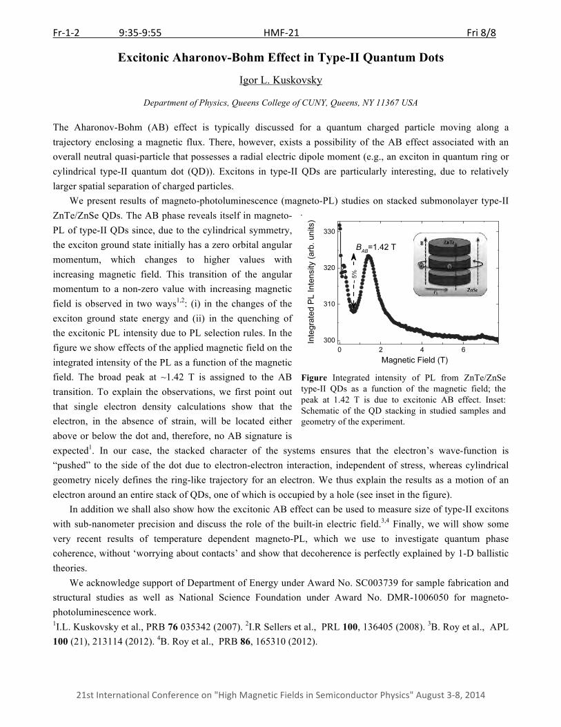
Fr-‐1-‐2 9:35-‐9:55 HMF-‐21 Fri 8/8
21st International Conference on "High Magnetic Fields in Semiconductor Physics" August 3-‐8, 2014
Excitonic Aharonov-Bohm Effect in Type-II Quantum Dots
Igor L. Kuskovsky
Department of Physics, Queens College of CUNY, Queens, NY 11367 USA
The Aharonov-Bohm (AB) effect is typically discussed for a quantum charged particle moving along a trajectory enclosing a magnetic flux. There, however, exists a possibility of the AB effect associated with an overall neutral quasi-particle that possesses a radial electric dipole moment (e.g., an exciton in quantum ring or cylindrical type-II quantum dot (QD)). Excitons in type-II QDs are particularly interesting, due to relatively larger spatial separation of charged particles.
We present results of magneto-photoluminescence (magneto-PL) studies on stacked submonolayer type-II ZnTe/ZnSe QDs. The AB phase reveals itself in magneto-PL of type-II QDs since, due to the cylindrical symmetry, the exciton ground state initially has a zero orbital angular momentum, which changes to higher values with increasing magnetic field. This transition of the angular momentum to a non-zero value with increasing magnetic field is observed in two ways1,2: (i) in the changes of the exciton ground state energy and (ii) in the quenching of the excitonic PL intensity due to PL selection rules. In the figure we show effects of the applied magnetic field on the integrated intensity of the PL as a function of the magnetic field. The broad peak at ~1.42 T is assigned to the AB transition. To explain the observations, we first point out that single electron density calculations show that the electron, in the absence of strain, will be located either above or below the dot and, therefore, no AB signature is expected1. In our case, the stacked character of the systems ensures that the electron’s wave-function is “pushed” to the side of the dot due to electron-electron interaction, independent of stress, whereas cylindrical geometry nicely defines the ring-like trajectory for an electron. We thus explain the results as a motion of an electron around an entire stack of QDs, one of which is occupied by a hole (see inset in the figure).
In addition we shall also show how the excitonic AB effect can be used to measure size of type-II excitons with sub-nanometer precision and discuss the role of the built-in electric field.3,4 Finally, we will show some very recent results of temperature dependent magneto-PL, which we use to investigate quantum phase coherence, without ‘worrying about contacts’ and show that decoherence is perfectly explained by 1-D ballistic theories.
We acknowledge support of Department of Energy under Award No. SC003739 for sample fabrication and structural studies as well as National Science Foundation under Award No. DMR-1006050 for magneto-photoluminescence work. 1I.L. Kuskovsky et al., PRB 76 035342 (2007). 2I.R Sellers et al., PRL 100, 136405 (2008). 3B. Roy et al., APL 100 (21), 213114 (2012). 4B. Roy et al., PRB 86, 165310 (2012).
Figure Integrated intensity of PL from ZnTe/ZnSe type-II QDs as a function of the magnetic field; the peak at 1.42 T is due to excitonic AB effect. Inset: Schematic of the QD stacking in studied samples and geometry of the experiment.
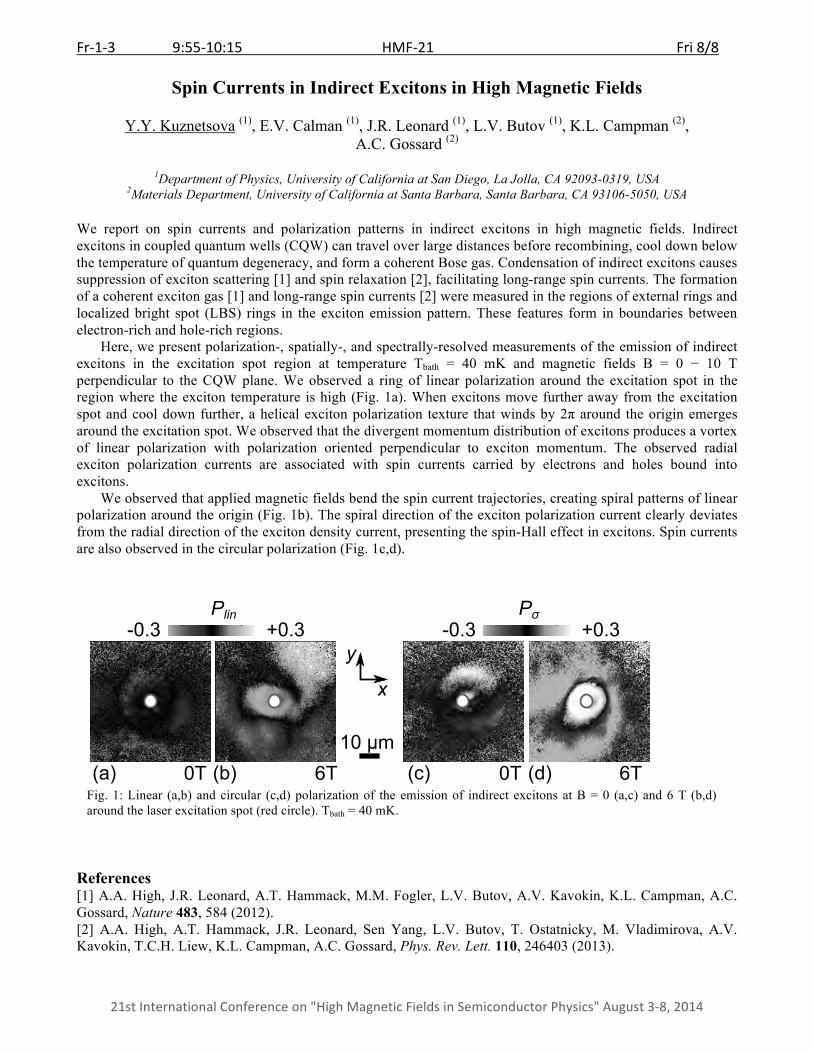
Fr-‐1-‐3 9:55-‐10:15 HMF-‐21 Fri 8/8
21st International Conference on "High Magnetic Fields in Semiconductor Physics" August 3-‐8, 2014
Spin Currents in Indirect Excitons in High Magnetic Fields
Y.Y. Kuznetsova (1), E.V. Calman (1), J.R. Leonard (1), L.V. Butov (1), K.L. Campman (2), A.C. Gossard (2)
1Department of Physics, University of California at San Diego, La Jolla, CA 92093-0319, USA
2Materials Department, University of California at Santa Barbara, Santa Barbara, CA 93106-5050, USA We report on spin currents and polarization patterns in indirect excitons in high magnetic fields. Indirect excitons in coupled quantum wells (CQW) can travel over large distances before recombining, cool down below the temperature of quantum degeneracy, and form a coherent Bose gas. Condensation of indirect excitons causes suppression of exciton scattering [1] and spin relaxation [2], facilitating long-range spin currents. The formation of a coherent exciton gas [1] and long-range spin currents [2] were measured in the regions of external rings and localized bright spot (LBS) rings in the exciton emission pattern. These features form in boundaries between electron-rich and hole-rich regions. Here, we present polarization-, spatially-, and spectrally-resolved measurements of the emission of indirect excitons in the excitation spot region at temperature Tbath = 40 mK and magnetic fields B = 0 − 10 T perpendicular to the CQW plane. We observed a ring of linear polarization around the excitation spot in the region where the exciton temperature is high (Fig. 1a). When excitons move further away from the excitation spot and cool down further, a helical exciton polarization texture that winds by 2π around the origin emerges around the excitation spot. We observed that the divergent momentum distribution of excitons produces a vortex of linear polarization with polarization oriented perpendicular to exciton momentum. The observed radial exciton polarization currents are associated with spin currents carried by electrons and holes bound into excitons. We observed that applied magnetic fields bend the spin current trajectories, creating spiral patterns of linear polarization around the origin (Fig. 1b). The spiral direction of the exciton polarization current clearly deviates from the radial direction of the exciton density current, presenting the spin-Hall effect in excitons. Spin currents are also observed in the circular polarization (Fig. 1c,d).
References [1] A.A. High, J.R. Leonard, A.T. Hammack, M.M. Fogler, L.V. Butov, A.V. Kavokin, K.L. Campman, A.C. Gossard, Nature 483, 584 (2012). [2] A.A. High, A.T. Hammack, J.R. Leonard, Sen Yang, L.V. Butov, T. Ostatnicky, M. Vladimirova, A.V. Kavokin, T.C.H. Liew, K.L. Campman, A.C. Gossard, Phys. Rev. Lett. 110, 246403 (2013).
������������ ��
����
��������
� �� � ��� ��� ���� �
�
�
Fig. 1: Linear (a,b) and circular (c,d) polarization of the emission of indirect excitons at B = 0 (a,c) and 6 T (b,d) around the laser excitation spot (red circle). Tbath = 40 mK.
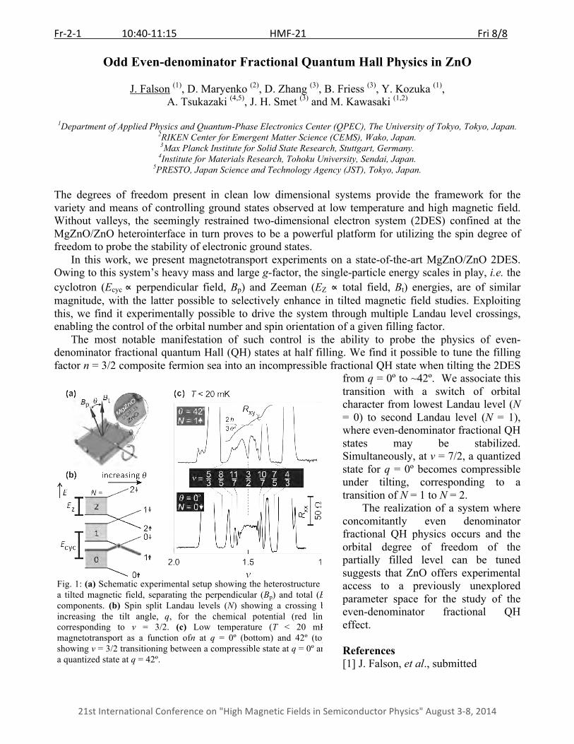
Fr-‐2-‐1 10:40-‐11:15 HMF-‐21 Fri 8/8
21st International Conference on "High Magnetic Fields in Semiconductor Physics" August 3-‐8, 2014
Fig. 1: (a) Schematic experimental setup showing the heterostructure in a tilted magnetic field, separating the perpendicular (Bp) and total (Bt) components. (b) Spin split Landau levels (N) showing a crossing by increasing the tilt angle, q, for the chemical potential (red line) corresponding to ν = 3/2. (c) Low temperature (T < 20 mK) magnetotransport as a function ofn at q = 0º (bottom) and 42º (top) showing ν = 3/2 transitioning between a compressible state at q = 0º and a quantized state at q = 42º.
Odd Even-denominator Fractional Quantum Hall Physics in ZnO
J. Falson (1), D. Maryenko (2), D. Zhang (3), B. Friess (3), Y. Kozuka (1), A. Tsukazaki (4,5), J. H. Smet (3) and M. Kawasaki (1,2)
1Department of Applied Physics and Quantum-Phase Electronics Center (QPEC), The University of Tokyo, Tokyo, Japan.
2RIKEN Center for Emergent Matter Science (CEMS), Wako, Japan. 3Max Planck Institute for Solid State Research, Stuttgart, Germany.
4Institute for Materials Research, Tohoku University, Sendai, Japan. 5PRESTO, Japan Science and Technology Agency (JST), Tokyo, Japan.
The degrees of freedom present in clean low dimensional systems provide the framework for the variety and means of controlling ground states observed at low temperature and high magnetic field. Without valleys, the seemingly restrained two-dimensional electron system (2DES) confined at the MgZnO/ZnO heterointerface in turn proves to be a powerful platform for utilizing the spin degree of freedom to probe the stability of electronic ground states.
In this work, we present magnetotransport experiments on a state-of-the-art MgZnO/ZnO 2DES. Owing to this system’s heavy mass and large g-factor, the single-particle energy scales in play, i.e. the cyclotron (Ecyc ∝ perpendicular field, Bp) and Zeeman (EZ ∝ total field, Bt) energies, are of similar magnitude, with the latter possible to selectively enhance in tilted magnetic field studies. Exploiting this, we find it experimentally possible to drive the system through multiple Landau level crossings, enabling the control of the orbital number and spin orientation of a given filling factor.
The most notable manifestation of such control is the ability to probe the physics of even-denominator fractional quantum Hall (QH) states at half filling. We find it possible to tune the filling factor n = 3/2 composite fermion sea into an incompressible fractional QH state when tilting the 2DES
from q = 0º to ~42º. We associate this transition with a switch of orbital character from lowest Landau level (N = 0) to second Landau level (N = 1), where even-denominator fractional QH states may be stabilized. Simultaneously, at ν = 7/2, a quantized state for q = 0º becomes compressible under tilting, corresponding to a transition of N = 1 to N = 2. The realization of a system where concomitantly even denominator fractional QH physics occurs and the orbital degree of freedom of the partially filled level can be tuned suggests that ZnO offers experimental access to a previously unexplored parameter space for the study of the even-denominator fractional QH effect. References [1] J. Falson, et al., submitted
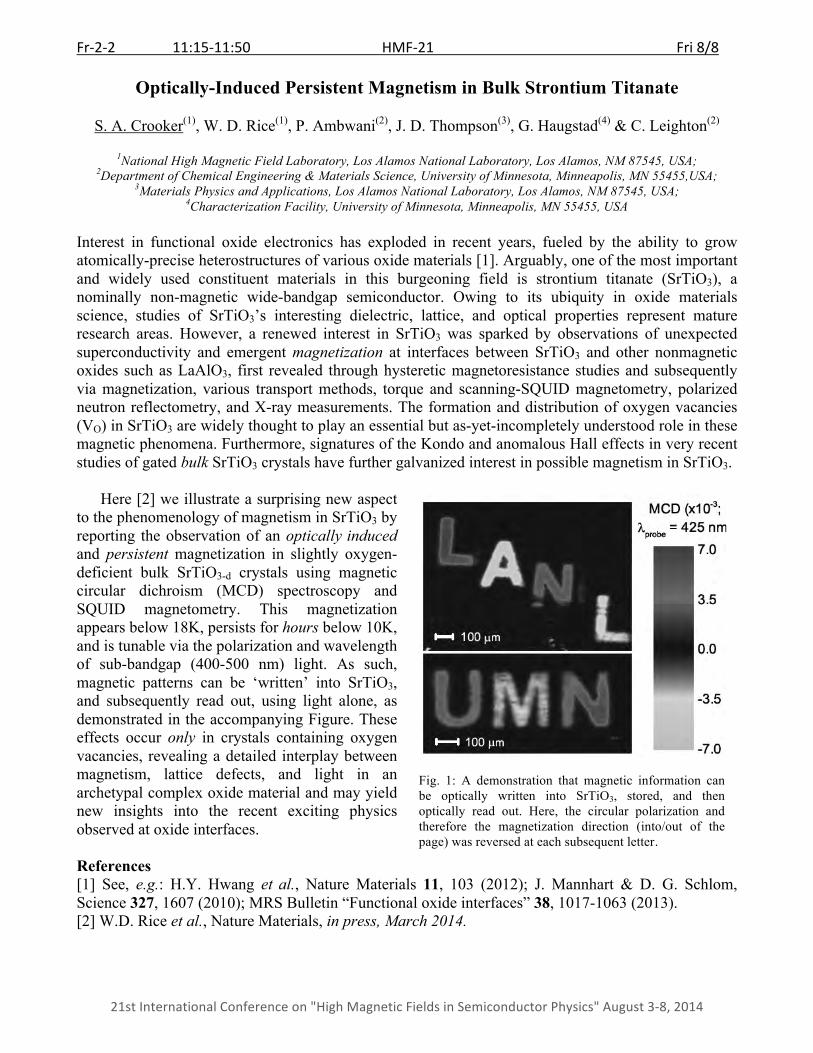
Fr-‐2-‐2 11:15-‐11:50 HMF-‐21 Fri 8/8
21st International Conference on "High Magnetic Fields in Semiconductor Physics" August 3-‐8, 2014
Optically-Induced Persistent Magnetism in Bulk Strontium Titanate
S. A. Crooker(1), W. D. Rice(1), P. Ambwani(2), J. D. Thompson(3), G. Haugstad(4) & C. Leighton(2)
1National High Magnetic Field Laboratory, Los Alamos National Laboratory, Los Alamos, NM 87545, USA;
2Department of Chemical Engineering & Materials Science, University of Minnesota, Minneapolis, MN 55455,USA; 3Materials Physics and Applications, Los Alamos National Laboratory, Los Alamos, NM 87545, USA;
4Characterization Facility, University of Minnesota, Minneapolis, MN 55455, USA Interest in functional oxide electronics has exploded in recent years, fueled by the ability to grow atomically-precise heterostructures of various oxide materials [1]. Arguably, one of the most important and widely used constituent materials in this burgeoning field is strontium titanate (SrTiO3), a nominally non-magnetic wide-bandgap semiconductor. Owing to its ubiquity in oxide materials science, studies of SrTiO3’s interesting dielectric, lattice, and optical properties represent mature research areas. However, a renewed interest in SrTiO3 was sparked by observations of unexpected superconductivity and emergent magnetization at interfaces between SrTiO3 and other nonmagnetic oxides such as LaAlO3, first revealed through hysteretic magnetoresistance studies and subsequently via magnetization, various transport methods, torque and scanning-SQUID magnetometry, polarized neutron reflectometry, and X-ray measurements. The formation and distribution of oxygen vacancies (VO) in SrTiO3 are widely thought to play an essential but as-yet-incompletely understood role in these magnetic phenomena. Furthermore, signatures of the Kondo and anomalous Hall effects in very recent studies of gated bulk SrTiO3 crystals have further galvanized interest in possible magnetism in SrTiO3.
Here [2] we illustrate a surprising new aspect to the phenomenology of magnetism in SrTiO3 by reporting the observation of an optically induced and persistent magnetization in slightly oxygen-deficient bulk SrTiO3-d crystals using magnetic circular dichroism (MCD) spectroscopy and SQUID magnetometry. This magnetization appears below 18K, persists for hours below 10K, and is tunable via the polarization and wavelength of sub-bandgap (400-500 nm) light. As such, magnetic patterns can be ‘written’ into SrTiO3, and subsequently read out, using light alone, as demonstrated in the accompanying Figure. These effects occur only in crystals containing oxygen vacancies, revealing a detailed interplay between magnetism, lattice defects, and light in an archetypal complex oxide material and may yield new insights into the recent exciting physics observed at oxide interfaces. References [1] See, e.g.: H.Y. Hwang et al., Nature Materials 11, 103 (2012); J. Mannhart & D. G. Schlom, Science 327, 1607 (2010); MRS Bulletin “Functional oxide interfaces” 38, 1017-1063 (2013). [2] W.D. Rice et al., Nature Materials, in press, March 2014.
Fig. 1: A demonstration that magnetic information can be optically written into SrTiO3, stored, and then optically read out. Here, the circular polarization and therefore the magnetization direction (into/out of the page) was reversed at each subsequent letter.
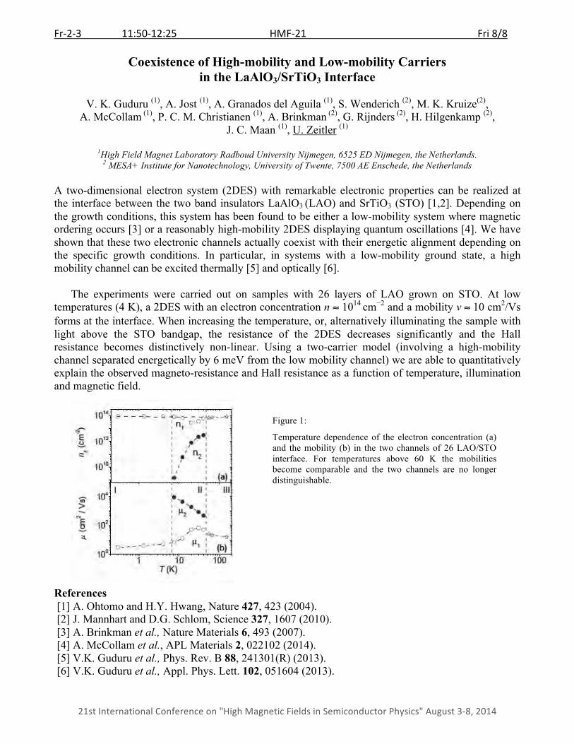
Fr-‐2-‐3 11:50-‐12:25 HMF-‐21 Fri 8/8
21st International Conference on "High Magnetic Fields in Semiconductor Physics" August 3-‐8, 2014
Coexistence of High-mobility and Low-mobility Carriers in the LaAlO3/SrTiO3 Interface
V. K. Guduru (1), A. Jost (1), A. Granados del Aguila (1), S. Wenderich (2), M. K. Kruize(2),
A. McCollam (1), P. C. M. Christianen (1), A. Brinkman (2), G. Rijnders (2), H. Hilgenkamp (2), J. C. Maan (1), U. Zeitler (1)
1High Field Magnet Laboratory Radboud University Nijmegen, 6525 ED Nijmegen, the Netherlands.
2 MESA+ Institute for Nanotechnology, University of Twente, 7500 AE Enschede, the Netherlands A two-dimensional electron system (2DES) with remarkable electronic properties can be realized at the interface between the two band insulators LaAlO3 (LAO) and SrTiO3 (STO) [1,2]. Depending on the growth conditions, this system has been found to be either a low-mobility system where magnetic ordering occurs [3] or a reasonably high-mobility 2DES displaying quantum oscillations [4]. We have shown that these two electronic channels actually coexist with their energetic alignment depending on the specific growth conditions. In particular, in systems with a low-mobility ground state, a high mobility channel can be excited thermally [5] and optically [6].
The experiments were carried out on samples with 26 layers of LAO grown on STO. At low temperatures (4 K), a 2DES with an electron concentration n ≈ 1014 cm−2 and a mobility ν ≈ 10 cm2/Vs forms at the interface. When increasing the temperature, or, alternatively illuminating the sample with light above the STO bandgap, the resistance of the 2DES decreases significantly and the Hall resistance becomes distinctively non-linear. Using a two-carrier model (involving a high-mobility channel separated energetically by 6 meV from the low mobility channel) we are able to quantitatively explain the observed magneto-resistance and Hall resistance as a function of temperature, illumination and magnetic field.
References [1] A. Ohtomo and H.Y. Hwang, Nature 427, 423 (2004). [2] J. Mannhart and D.G. Schlom, Science 327, 1607 (2010). [3] A. Brinkman et al., Nature Materials 6, 493 (2007). [4] A. McCollam et al., APL Materials 2, 022102 (2014). [5] V.K. Guduru et al., Phys. Rev. B 88, 241301(R) (2013). [6] V.K. Guduru et al., Appl. Phys. Lett. 102, 051604 (2013).
Figure 1:
Temperature dependence of the electron concentration (a) and the mobility (b) in the two channels of 26 LAO/STO interface. For temperatures above 60 K the mobilities become comparable and the two channels are no longer distinguishable.
21st International Conference on "High Magnetic Fields in Semiconductor Physics" August 3-‐8, 2014
HMF-21
Posters


Poster ID: P1 HMF-‐21 Mon-‐Tue 8/4 -‐8/5
21st International Conference on "High Magnetic Fields in Semiconductor Physics" August 3-‐8, 2014
Capacitance signature of interlayer exciton formation in double layer quantum Hall systems
B. Skinner (1), B. I. Shklovskii (2)
1Materials Science Division, Argonne National Laboratory, Argonne, IL USA
2Fine Theoretical Physics Institute, University of Minnesota, Minneapolis, MN USA When a large perpendicular magnetic field is applied to a thin double layer electron system, electrons in one layer can bind strongly to holes in the other layer, forming interlayer excitons[1]. Such excitons interact only via a weak dipole-dipole interaction, and this allows them to have a large compressibility. This large compressibility implies an anomalous enhancement of the interlayer capacitance that can be measured experimentally[2, 3].
In this talk we consider the interlayer capacitance of such a double-layer electron-hole system, focusing primarily on double-layer graphene with total filling factor zero. The capacitance is calculated as a function of electron density and interlayer distance, and large capacitance enhancement is shown to arise in the limit of low exciton density and small interlayer distance. The expected signature of exciton formation and exciton condensation in the measured capacitance are discussed.
References [1] J. P. Eisenstein and A. H. MacDonald, Nature, 432, 691 (2004). [2] B. Skinner and B. I. Shklovskii, Phys. Rev. B., 87, 035409 (2013). [3] B. Skinner, G. L. Yu, A. V. Kretinin, A. K. Geim, K. S. Novoselov, and B. I. Shklovskii, Phys. Rev. B, 88, 155417 (2013).
Fig. 1: Schematic illustration of a double layer system in which electrons in the top layer couple strongly to holes in the bottom layer. The size of the electron and hole wavefunctions are given by the magnetic length lB.

Poster ID: P2 HMF-‐21 Mon-‐Tue 8/4 -‐8/5
21st International Conference on "High Magnetic Fields in Semiconductor Physics" August 3-‐8, 2014
Wave functions of the 2/5 filled quantum Hall ground state
R. E. Wooten (1), J. H. Macek (1), J. J. Quinn (1)
1University of Tennessee, Knoxville, USA
The N-electron wave function Ψ of lowest Landau level of a quantum Hall system can be expressed in terms of the product of an antisymmetric Fermion factor F{zij} = Πi<j(zij), and a symmetric correlation function G{zij}. Here, zij = zi – zj, and zi = xi – iyi is the coordinate of the ith particle on the complex plane. An integer 2l, where l is the single particle angular momentum, defines the Hilbert space of the problem. The maximum allowed power of zi in Ψ is equal to 2l. G{zij} will involve a sum of terms consisting of products of correlation factors zij. For a state of total angular momentum L = 0, G{zij} can be written as a homogeneous polynomial of total degree KG = Nl - N(N-1)/2. The terms in G can be represented by diagrams in which a factor zij is represented by a line connecting particles i and j. No diagram contributing to G can have more than 2l+1-N lines emanating from any particle i. We define n2 as the number of pairs in a correlation diagram connected by a correlation factor zij
2 (for any i and j), n1 as the number connected by a factor zij, and n0 as the number with no correlation factors. Then the number of pairs is equal to KF = n2 + n1 + n0, KG = 2n2+n1, and K = KF+KG = Nl. For a simple system of N = 6 particles (2l = 11), it is possible to construct diagrams with values of (n2, n1, n0) ranging from (9, 0, 6) to (3, 12, 0). The conditions that contributions to G must satisfy greatly restrict the choices for the function. In Fig. 1, we show one possible diagram contributing to G selected from the choice (n2, n1, n0) = (6, 6, 3). The wave function Ψ is proportional to F*G. We have compared the normalized wave function with the one obtained by numerical diagonalization of the Coulomb interaction for N = 6. The overlap is more than 98%. This came as a surprise because we had expected that the correlations for the lowest
L = 0 state would involve partitions of N = 6 into two subsets containing 2 and 4 particles, since Jain’s description of the ν = 2/5 state has two filled Composite Fermion (CF) levels with two particles occupying the lowest CF level with angular momentum lCF0 = ½, and four CFs occupying the next CF level with angular momentum lCF1 = 3/2. At the moment we have no intuitive understanding of why Fig. 1, with no apparent 2/4 partitioning, gives the lowest energy state. We are investigating other values of (n2, n1, n0).
12
3
4 5
6
Figure 1. Sample correlation diagrams selected from (n2, n1, n0) = (6, 6, 3). G{zij} = S6{z12
2z13z15z162z23z24z26
2z342z35
2z452z46z56}. Here,
S6 symmetrizes the factor in curly brackets over all particles.
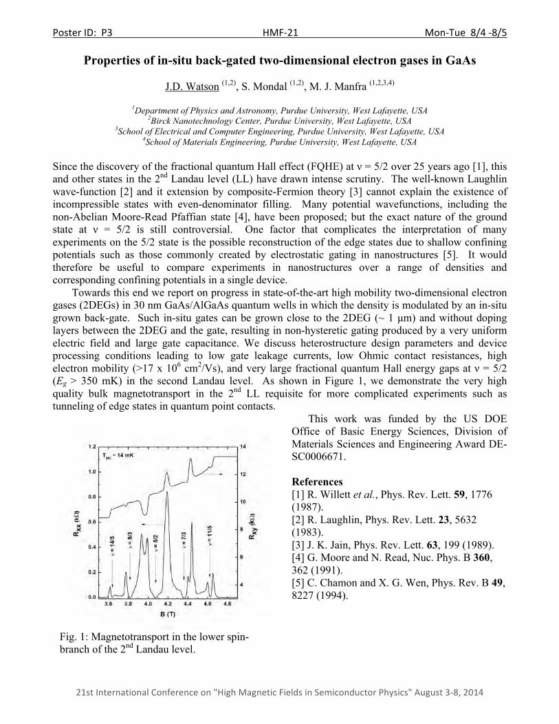
Poster ID: P3 HMF-‐21 Mon-‐Tue 8/4 -‐8/5
21st International Conference on "High Magnetic Fields in Semiconductor Physics" August 3-‐8, 2014
Properties of in-situ back-gated two-dimensional electron gases in GaAs
J.D. Watson (1,2), S. Mondal (1,2), M. J. Manfra (1,2,3,4)
1Department of Physics and Astronomy, Purdue University, West Lafayette, USA 2Birck Nanotechnology Center, Purdue University, West Lafayette, USA
3School of Electrical and Computer Engineering, Purdue University, West Lafayette, USA 4School of Materials Engineering, Purdue University, West Lafayette, USA
Since the discovery of the fractional quantum Hall effect (FQHE) at ν = 5/2 over 25 years ago [1], this and other states in the 2nd Landau level (LL) have drawn intense scrutiny. The well-known Laughlin wave-function [2] and it extension by composite-Fermion theory [3] cannot explain the existence of incompressible states with even-denominator filling. Many potential wavefunctions, including the non-Abelian Moore-Read Pfaffian state [4], have been proposed; but the exact nature of the ground state at ν = 5/2 is still controversial. One factor that complicates the interpretation of many experiments on the 5/2 state is the possible reconstruction of the edge states due to shallow confining potentials such as those commonly created by electrostatic gating in nanostructures [5]. It would therefore be useful to compare experiments in nanostructures over a range of densities and corresponding confining potentials in a single device. Towards this end we report on progress in state-of-the-art high mobility two-dimensional electron gases (2DEGs) in 30 nm GaAs/AlGaAs quantum wells in which the density is modulated by an in-situ grown back-gate. Such in-situ gates can be grown close to the 2DEG (~ 1 µm) and without doping layers between the 2DEG and the gate, resulting in non-hysteretic gating produced by a very uniform electric field and large gate capacitance. We discuss heterostructure design parameters and device processing conditions leading to low gate leakage currents, low Ohmic contact resistances, high electron mobility (>17 x 106 cm2/Vs), and very large fractional quantum Hall energy gaps at ν = 5/2 (Eg > 350 mK) in the second Landau level. As shown in Figure 1, we demonstrate the very high quality bulk magnetotransport in the 2nd LL requisite for more complicated experiments such as tunneling of edge states in quantum point contacts.
This work was funded by the US DOE Office of Basic Energy Sciences, Division of Materials Sciences and Engineering Award DE-SC0006671.
References [1] R. Willett et al., Phys. Rev. Lett. 59, 1776 (1987). [2] R. Laughlin, Phys. Rev. Lett. 23, 5632 (1983). [3] J. K. Jain, Phys. Rev. Lett. 63, 199 (1989). [4] G. Moore and N. Read, Nuc. Phys. B 360, 362 (1991). [5] C. Chamon and X. G. Wen, Phys. Rev. B 49, 8227 (1994).
Fig. 1: Magnetotransport in the lower spin-branch of the 2nd Landau level.
Poster ID: P4 HMF-‐21 Mon-‐Tue 8/4 -‐8/5
21st International Conference on "High Magnetic Fields in Semiconductor Physics" August 3-‐8, 2014
Quantum Well Symmetry and the Orientation of the Quantum Hall Stripe Phases
J. Pollanen (1), J.P. Eisenstein (1), L.N. Pfeiffer (2), and K.W. West (2)
1Institute for Quantum Information and Matter (IQIM), California Institute of Technology, Pasadena, California, USA 2Department of Electrical Engineering, Princeton University, Princeton, New Jersey, USA
High quality two dimensional electron systems (2DES) in GaAs can exhibit large transport anisotropies in the vicinity of half-filled excited Landau levels [1,2]. These anisotropies are associated with the formation of collective electron states possessing broken rotational symmetry in the plane of the 2DES. These states, known as the quantum Hall stripe phases, appear to be among the first known examples of purely electronic nematic liquid crystals. Experiments show that the orientation of the stripes is locked relative to the crystallographic axes of the GaAs host lattice. Unambiguous identification of the native symmetry-breaking potential remains an open question and an active area of interest, both theoretically and experimentally. Various symmetry-breaking mechanisms have been proposed to couple to the stripes and establish their orientation, e.g. anisotropic band structure [3], piezoelectricity [4], strain [5] and, recently, the competition between Rashba and Dresselhaus spin-orbit couplings [6]. Noting that piezoelectricity, strain and spin-orbit effects can be altered by the symmetry of the electronic confinement potential, we have performed magneto-transport experiments on samples in which we have systematically varied the symmetry of the GaAs quantum well either by asymmetric doping or with front and backside electrostatic gates. These samples allow us to study the effect, at fixed 2D electron density, of quantum well symmetry on the orientation of the quantum Hall stripe phases.
References [1] M.P. Lilly et al. Phys. Rev. Lett. 82, 394 (1999) [2] R.R. Du et al. Solid State Commun. 109, 389 (1999) [3] B. Rosenow and S. Scheidl, Int. J. of Mod. Phys. B 15, 1905 (2001) [4] D.V. Fil, Sov. J. Low Temp. Phys. 26, 581 (2000). [5] S.P. Kovudayur et al. Phys. Rev. Lett. 106, 016804 (2011) [6] I. Sodemann and A.H. MacDonald, arXiv:1302.3896 (2013)
Poster ID: P5 HMF-‐21 Mon-‐Tue 8/4 -‐8/5
21st International Conference on "High Magnetic Fields in Semiconductor Physics" August 3-‐8, 2014
Optical emission from competing quantum phases of the second Landau Level
A. L. Levy(1), U. Wurstbauer(2), A. Pinczuk(1), M. Manfra(3), J. Watson(3), S. Mondal(3), L. N. Pfeiffer(4), K. W. West(4)
1Columbia University, New York, New York, United States
2Technical University of Munich, Garching, Germany 3Purdue University, West Lafayette, Indiana, United States
4Princeton University, Princeton, New Jersey, United States Fractional quantum Hall states in the range of filling factors 4≥ν≥2 of the second (N=1) Landau level have been the subject of intense study due to their exhibition of striking phenomena. Much of these states' physics is dominated by the competition and coexistence of quantum phases. Numerous previous works have sought to probe these electron systems by magneto-transport experiments to seek understandings of these striking, yet subtle, quantum phases of electron systems.
The work reported here explores the use of photoluminescence (PL) emission from the N=1 Landau level to probe the competition between the quantum phases. We present results in which competing phases in these filling factors manifest through optical emission originating in the N=1 Landau Level with unprecedented clarity: specifically, through the dependence of the emergence and disappearance of PL peaks on filling factor.
The optical experiments are in symmetrically modulation-doped GaAs quantum of exceptional electron mobility. Cold finger temperatures in a dilution refrigerator are below 40mK. Resonant Rayleigh spectra at taken at some of the filling factor of the N=1 Landau level enable the identification of condensed states of the 2D electron system. Parallels between PL data with those in resonant inelastic light scattering by spin waves reveal links between optical emission bands and spin polarization in the 2D electron system.
PL spectra in a range about ν=7/3=2+1/3 is being compared with extensively studied optical emission near ν=1/3 (Ref [1] is one example) to seek evidence on characteristics of the quasiparticles that manifest in optical emission transitions from the N=1 Landau level. This approach is one of several venues to explore the competing quantum phases of the second Landau levels. PL spectroscopy in the N=1 Landau level offers great promise to advance the understanding of striking impact of electron interactions in the emergence of competing quantum phases in the second Landau level. This work is supported by the U.S. National Science Foundation. References [1] M. Byszewski et al. Nature Physics 2, 239-243 (2006)
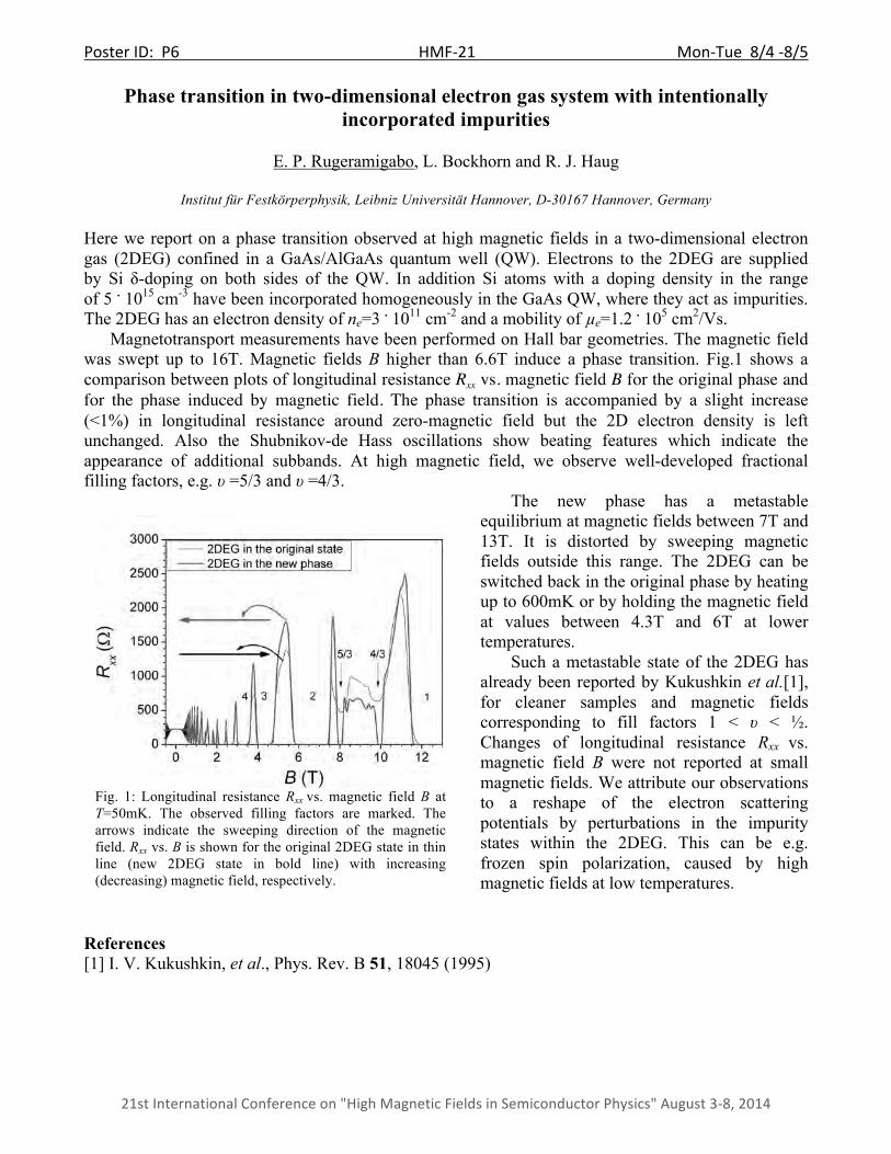
Poster ID: P6 HMF-‐21 Mon-‐Tue 8/4 -‐8/5
21st International Conference on "High Magnetic Fields in Semiconductor Physics" August 3-‐8, 2014
Phase transition in two-dimensional electron gas system with intentionally incorporated impurities
E. P. Rugeramigabo, L. Bockhorn and R. J. Haug
Institut für Festkörperphysik, Leibniz Universität Hannover, D-30167 Hannover, Germany
Here we report on a phase transition observed at high magnetic fields in a two-dimensional electron gas (2DEG) confined in a GaAs/AlGaAs quantum well (QW). Electrons to the 2DEG are supplied by Si δ-doping on both sides of the QW. In addition Si atoms with a doping density in the range of 5 . 1015 cm-3 have been incorporated homogeneously in the GaAs QW, where they act as impurities. The 2DEG has an electron density of ne=3 . 1011 cm-2 and a mobility of µe=1.2 . 105 cm2/Vs.
Magnetotransport measurements have been performed on Hall bar geometries. The magnetic field was swept up to 16T. Magnetic fields B higher than 6.6T induce a phase transition. Fig.1 shows a comparison between plots of longitudinal resistance Rxx vs. magnetic field B for the original phase and for the phase induced by magnetic field. The phase transition is accompanied by a slight increase (<1%) in longitudinal resistance around zero-magnetic field but the 2D electron density is left unchanged. Also the Shubnikov-de Hass oscillations show beating features which indicate the appearance of additional subbands. At high magnetic field, we observe well-developed fractional filling factors, e.g. υ =5/3 and υ =4/3.
The new phase has a metastable equilibrium at magnetic fields between 7T and 13T. It is distorted by sweeping magnetic fields outside this range. The 2DEG can be switched back in the original phase by heating up to 600mK or by holding the magnetic field at values between 4.3T and 6T at lower temperatures. Such a metastable state of the 2DEG has already been reported by Kukushkin et al.[1], for cleaner samples and magnetic fields corresponding to fill factors 1 < υ < ½. Changes of longitudinal resistance Rxx vs. magnetic field B were not reported at small magnetic fields. We attribute our observations to a reshape of the electron scattering potentials by perturbations in the impurity states within the 2DEG. This can be e.g. frozen spin polarization, caused by high magnetic fields at low temperatures.
References [1] I. V. Kukushkin, et al., Phys. Rev. B 51, 18045 (1995)
Fig. 1: Longitudinal resistance Rxx vs. magnetic field B at T=50mK. The observed filling factors are marked. The arrows indicate the sweeping direction of the magnetic field. Rxx vs. B is shown for the original 2DEG state in thin line (new 2DEG state in bold line) with increasing (decreasing) magnetic field, respectively.

Poster ID: P7 HMF-‐21 Mon-‐Tue 8/4 -‐8/5
21st International Conference on "High Magnetic Fields in Semiconductor Physics" August 3-‐8, 2014
Evidence of a Warped Fermi Contour for Hole-flux Composite Fermions
M.A. Mueed,1 D. Kamburov,1 L.N. Pfeiffer,1 K.W. West,1 K.W. Baldwin,1 R. Winkler,2 M. Shayegan1
1Department of Electrical Engineering, Princeton, NJ, USA
2Department of Physics, Northern Illinois University, DeKalb, IL, USA Composite fermions (CFs), quasi-particles formed by attaching an even number of flux quanta to each carrier in high perpendicular magnetic fields (B), capture many phenomena exhibited by an interacting system of two-dimensional (2D) carriers such as the fractional quantum Hall effect. The flux attachment cancels out the external B at a half-filled Landau level, enabling CFs to occupy a Fermi sea and possess a Fermi contour, similar to their B = 0 carrier counterparts. Because the CFs are primarily a manifestation of interaction, one might argue that their physical properties should retain no memory of the B = 0 particles, including their energy band structure. Here we present tantalizing evidence through commensurability measurements that hole-flux CFs confined to a wide GaAs quantum well (QW) exhibit a warped Fermi contour qualitatively similar to their B = 0 hole counterparts. In commensurability experiments, a resistance minimum is observed in the longitudinal resistance (Rxx) when the quasi-classical CF cyclotron orbit diameter becomes commensurate with the period of the modulation [1,2]. The field position of the minimum provides a direct measure of the Fermi wave vector (kF) .As illustrated in Fig. 1(a), the Fermi contour of 2D holes confined to a wide GaAs QW is expected to be significantly warped. Our low-field commensurability measurements on 2D holes in a 35-nm QW indeed demonstrate such warping, with kF
along [110] being about 20% larger than kF expected if the hole Fermi contour were circular; this is
consistent with the average warping (~25%) calculated for the two spin species whose contours are split because of the spin-orbit interaction [3]. Data of Figs. 1(b) and 1(c) show that the CFs, too, exhibit a warped Fermi contour! As clearly seen in Fig. 1(c), the positions of the observed Rxx minima (vertical arrows) are measurably farther from where we would expect the minima if the CF Fermi contour were circular (red tick marks). From the observed positions, we deduce a warping of about 10%. Our results demonstrate that the warping of the hole Fermi contour is partly transferred to the hole-flux CFs. Complementing the recent measurements which have shown that the CF Fermi contours can be distorted via the application of a parallel magnetic field [2], our data illustrate that the band structure of the B = 0 particles can directly affect the CF Fermi contour.
References [1] J.H. Smet et al., PRL 83, 2620 (1999). [2] D. Kamburov et al., PRL 109, 236401 (2012); PRL 110, 206801 (2013); PRB 89, 085304 (2014). [3] In our measurements we cannot reslove the two Fermi contours for the two spin species.
FIG. 1: (a) Calculated Fermi contours of 2D holes confined to a wide GaAs QW, exhibiting significant warping. The calculations are for B = 0. (b) High-field Rxx vs B data for 2D holes confined to a 35-nm-wide GaAs QW and subjected to a unidirectional lateral potential modualtion of period 200 nm. The strong Rxx minima observed on the two sides of ν = ½ signal the commensurabily of the CF classical cyclotron orbit diameter with the period of the modulation. As seen in (c), the positions of these minima are measurably farther than expected for a circular Fermi contour for fully spin polarized CFs (marked by vertical red tick-marks).
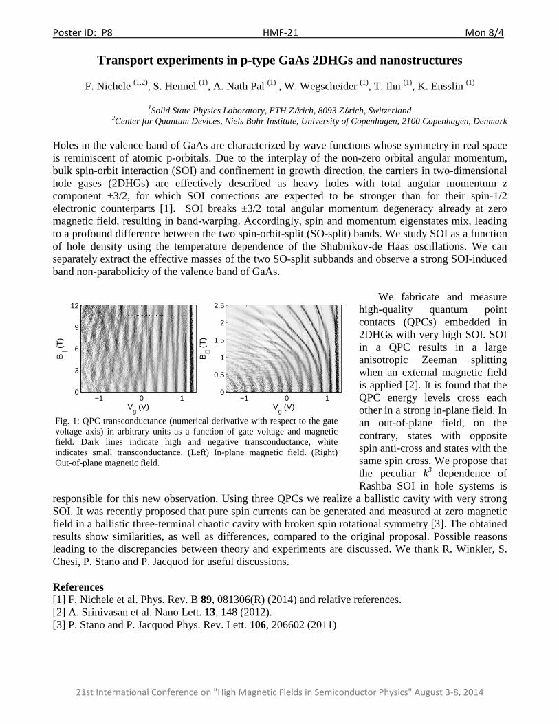
Poster ID: P8 HMF-21 Mon 8/4
21st International Conference on "High Magnetic Fields in Semiconductor Physics" August 3-8, 2014
Transport experiments in p-type GaAs 2DHGs and nanostructures
F. Nichele (1,2), S. Hennel (1), A. Nath Pal (1) , W. Wegscheider (1), T. Ihn (1), K. Ensslin (1)
1Solid State Physics Laboratory, ETH Zürich, 8093 Zürich, Switzerland 2Center for Quantum Devices, Niels Bohr Institute, University of Copenhagen, 2100 Copenhagen, Denmark
Holes in the valence band of GaAs are characterized by wave functions whose symmetry in real space is reminiscent of atomic p-orbitals. Due to the interplay of the non-zero orbital angular momentum, bulk spin-orbit interaction (SOI) and confinement in growth direction, the carriers in two-dimensional hole gases (2DHGs) are effectively described as heavy holes with total angular momentum z component ±3/2, for which SOI corrections are expected to be stronger than for their spin-1/2 electronic counterparts [1]. SOI breaks ±3/2 total angular momentum degeneracy already at zero magnetic field, resulting in band-warping. Accordingly, spin and momentum eigenstates mix, leading to a profound difference between the two spin-orbit-split (SO-split) bands. We study SOI as a function of hole density using the temperature dependence of the Shubnikov-de Haas oscillations. We can separately extract the effective masses of the two SO-split subbands and observe a strong SOI-induced band non-parabolicity of the valence band of GaAs.
We fabricate and measure high-quality quantum point contacts (QPCs) embedded in 2DHGs with very high SOI. SOI in a QPC results in a large anisotropic Zeeman splitting when an external magnetic field is applied [2]. It is found that the QPC energy levels cross each other in a strong in-plane field. In an out-of-plane field, on the contrary, states with opposite spin anti-cross and states with the same spin cross. We propose that the peculiar k3 dependence of Rashba SOI in hole systems is
responsible for this new observation. Using three QPCs we realize a ballistic cavity with very strong SOI. It was recently proposed that pure spin currents can be generated and measured at zero magnetic field in a ballistic three-terminal chaotic cavity with broken spin rotational symmetry [3]. The obtained results show similarities, as well as differences, compared to the original proposal. Possible reasons leading to the discrepancies between theory and experiments are discussed. We thank R. Winkler, S. Chesi, P. Stano and P. Jacquod for useful discussions. References [1] F. Nichele et al. Phys. Rev. B 89, 081306(R) (2014) and relative references. [2] A. Srinivasan et al. Nano Lett. 13, 148 (2012). [3] P. Stano and P. Jacquod Phys. Rev. Lett. 106, 206602 (2011)
Vg (V)
−1 0 10
0.5
1
1.5
2
2.5
B⊥ (
T)
Vg (V)
−1 0 10
3
6
9
12
B|| (
T)
Fig. 1: QPC transconductance (numerical derivative with respect to the gate voltage axis) in arbitrary units as a function of gate voltage and magnetic field. Dark lines indicate high and negative transconductance, white indicates small transconductance. (Left) In-plane magnetic field. (Right) Out-of-plane magnetic field.
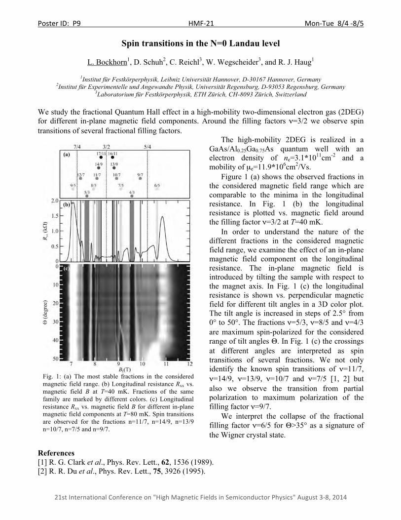
Poster ID: P9 HMF-‐21 Mon-‐Tue 8/4 -‐8/5
21st International Conference on "High Magnetic Fields in Semiconductor Physics" August 3-‐8, 2014
Spin transitions in the N=0 Landau level
L. Bockhorn1, D. Schuh2, C. Reichl3, W. Wegscheider3, and R. J. Haug1
1Institut für Festkörperphysik, Leibniz Universität Hannover, D-30167 Hannover, Germany 2Institut für Experimentelle und Angewandte Physik, Universität Regensburg, D-93053 Regensburg, Germany
3Laboratorium für Festkörperphysik, ETH Zürich, CH-8093 Zürich, Switzerland
We study the fractional Quantum Hall effect in a high-mobility two-dimensional electron gas (2DEG) for different in-plane magnetic field components. Around the filling factors ν=3/2 we observe spin transitions of several fractional filling factors.
The high-mobility 2DEG is realized in a GaAs/Al0.25Ga0.75As quantum well with an electron density of ne=3.1*1011cm-2 and a mobility of µe=11.9*106cm2/Vs. Figure 1 (a) shows the observed fractions in the considered magnetic field range which are comparable to the minima in the longitudinal resistance. In Fig. 1 (b) the longitudinal resistance is plotted vs. magnetic field around the filling factor ν=3/2 at T=40 mK. In order to understand the nature of the different fractions in the considered magnetic field range, we examine the effect of an in-plane magnetic field component on the longitudinal resistance. The in-plane magnetic field is introduced by tilting the sample with respect to the magnet axis. In Fig. 1 (c) the longitudinal resistance is shown vs. perpendicular magnetic field for different tilt angles in a 3D color plot. The tilt angle is increased in steps of 2.5° from 0° to 50°. The fractions ν=5/3, ν=8/5 and ν=4/3 are maximum spin-polarized for the considered range of tilt angles Θ. In Fig. 1 (c) the crossings at different angles are interpreted as spin transitions of several fractions. We not only identify the known spin transitions of ν=11/7, ν=14/9, ν=13/9, ν=10/7 and ν=7/5 [1, 2] but also we observe the transition from partial polarization to maximum polarization of the filling factor ν=9/7. We interpret the collapse of the fractional filling factor ν=6/5 for Θ>35° as a signature of the Wigner crystal state.
References [1] R. G. Clark et al., Phys. Rev. Lett., 62, 1536 (1989). [2] R. R. Du et al., Phys. Rev. Lett., 75, 3926 (1995).
Fig. 1: (a) The most stable fractions in the considered magnetic field range. (b) Longitudinal resistance Rxx vs. magnetic field B at T=40 mK. Fractions of the same family are marked by different colors. (c) Longitudinal resistance Rxx vs. magnetic field B for different in-plane magnetic field components at T=80 mK. Spin transitions are observed for the fractions n=11/7, n=14/9, n=13/9 n=10/7, n=7/5 and n=9/7.
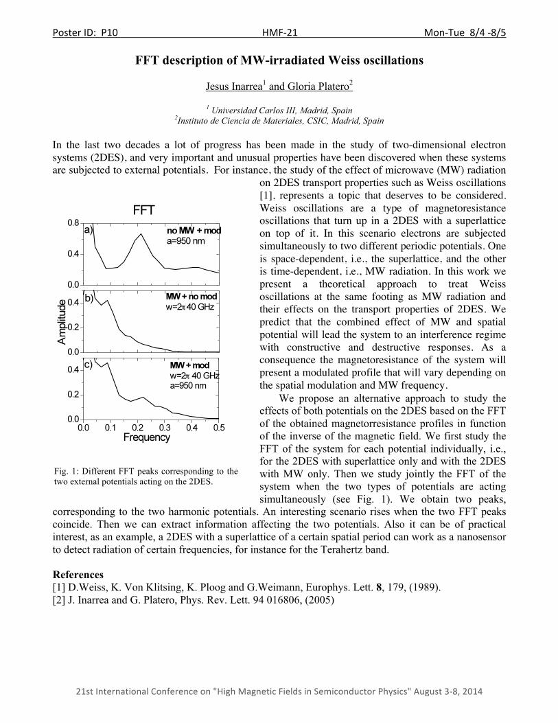
Poster ID: P10 HMF-‐21 Mon-‐Tue 8/4 -‐8/5
21st International Conference on "High Magnetic Fields in Semiconductor Physics" August 3-‐8, 2014
FFT description of MW-irradiated Weiss oscillations
Jesus Inarrea1 and Gloria Platero2
1 Universidad Carlos III, Madrid, Spain
2Instituto de Ciencia de Materiales, CSIC, Madrid, Spain In the last two decades a lot of progress has been made in the study of two-dimensional electron systems (2DES), and very important and unusual properties have been discovered when these systems are subjected to external potentials. For instance, the study of the effect of microwave (MW) radiation
on 2DES transport properties such as Weiss oscillations [1], represents a topic that deserves to be considered. Weiss oscillations are a type of magnetoresistance oscillations that turn up in a 2DES with a superlattice on top of it. In this scenario electrons are subjected simultaneously to two different periodic potentials. One is space-dependent, i.e., the superlattice, and the other is time-dependent, i.e., MW radiation. In this work we present a theoretical approach to treat Weiss oscillations at the same footing as MW radiation and their effects on the transport properties of 2DES. We predict that the combined effect of MW and spatial potential will lead the system to an interference regime with constructive and destructive responses. As a consequence the magnetoresistance of the system will present a modulated profile that will vary depending on the spatial modulation and MW frequency. We propose an alternative approach to study the effects of both potentials on the 2DES based on the FFT of the obtained magnetorresistance profiles in function of the inverse of the magnetic field. We first study the FFT of the system for each potential individually, i.e., for the 2DES with superlattice only and with the 2DES with MW only. Then we study jointly the FFT of the system when the two types of potentials are acting simultaneously (see Fig. 1). We obtain two peaks,
corresponding to the two harmonic potentials. An interesting scenario rises when the two FFT peaks coincide. Then we can extract information affecting the two potentials. Also it can be of practical interest, as an example, a 2DES with a superlattice of a certain spatial period can work as a nanosensor to detect radiation of certain frequencies, for instance for the Terahertz band. References [1] D.Weiss, K. Von Klitsing, K. Ploog and G.Weimann, Europhys. Lett. 8, 179, (1989). [2] J. Inarrea and G. Platero, Phys. Rev. Lett. 94 016806, (2005)
Fig. 1: Different FFT peaks corresponding to the two external potentials acting on the 2DES.
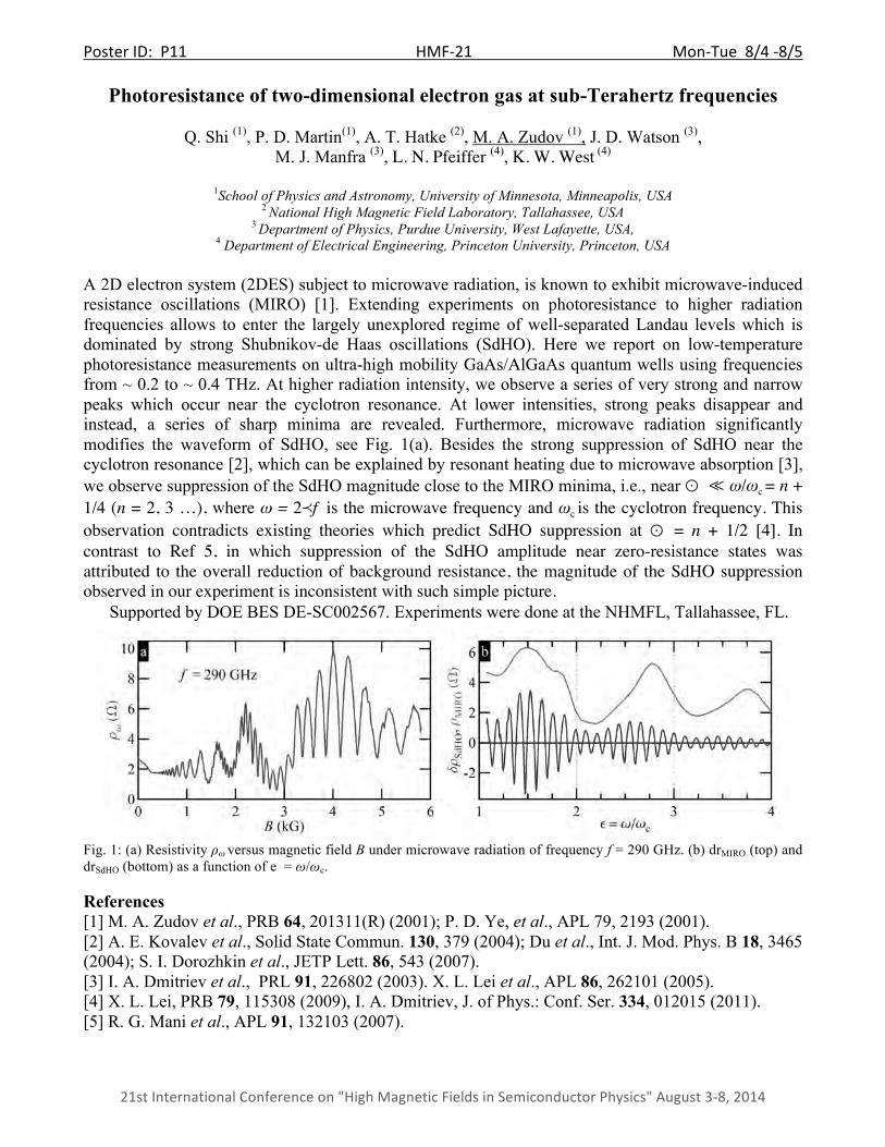
Poster ID: P11 HMF-‐21 Mon-‐Tue 8/4 -‐8/5
21st International Conference on "High Magnetic Fields in Semiconductor Physics" August 3-‐8, 2014
Photoresistance of two-dimensional electron gas at sub-Terahertz frequencies
Q. Shi (1), P. D. Martin(1), A. T. Hatke (2), M. A. Zudov (1), J. D. Watson (3), M. J. Manfra (3), L. N. Pfeiffer (4), K. W. West (4)
1School of Physics and Astronomy, University of Minnesota, Minneapolis, USA
2 National High Magnetic Field Laboratory, Tallahassee, USA 3 Department of Physics, Purdue University, West Lafayette, USA,
4 Department of Electrical Engineering, Princeton University, Princeton, USA A 2D electron system (2DES) subject to microwave radiation, is known to exhibit microwave-induced resistance oscillations (MIRO) [1]. Extending experiments on photoresistance to higher radiation frequencies allows to enter the largely unexplored regime of well-separated Landau levels which is dominated by strong Shubnikov-de Haas oscillations (SdHO). Here we report on low-temperature photoresistance measurements on ultra-high mobility GaAs/AlGaAs quantum wells using frequencies from ~ 0.2 to ~ 0.4 THz. At higher radiation intensity, we observe a series of very strong and narrow peaks which occur near the cyclotron resonance. At lower intensities, strong peaks disappear and instead, a series of sharp minima are revealed. Furthermore, microwave radiation significantly modifies the waveform of SdHO, see Fig. 1(a). Besides the strong suppression of SdHO near the cyclotron resonance [2], which can be explained by resonant heating due to microwave absorption [3], we observe suppression of the SdHO magnitude close to the MIRO minima, i.e., near ⊙ ≪ ω/ωc = n + 1/4 (n = 2, 3 …), where ω = 2≺f is the microwave frequency and ωc is the cyclotron frequency. This observation contradicts existing theories which predict SdHO suppression at ⊙ = n + 1/2 [4]. In contrast to Ref 5, in which suppression of the SdHO amplitude near zero-resistance states was attributed to the overall reduction of background resistance, the magnitude of the SdHO suppression observed in our experiment is inconsistent with such simple picture.
Supported by DOE BES DE-SC002567. Experiments were done at the NHMFL, Tallahassee, FL.
Fig. 1: (a) Resistivity ρω versus magnetic field B under microwave radiation of frequency f = 290 GHz. (b) drMIRO (top) and drSdHO (bottom) as a function of e = ω/ωc. References [1] M. A. Zudov et al., PRB 64, 201311(R) (2001); P. D. Ye, et al., APL 79, 2193 (2001). [2] A. E. Kovalev et al., Solid State Commun. 130, 379 (2004); Du et al., Int. J. Mod. Phys. B 18, 3465 (2004); S. I. Dorozhkin et al., JETP Lett. 86, 543 (2007). [3] I. A. Dmitriev et al., PRL 91, 226802 (2003). X. L. Lei et al., APL 86, 262101 (2005). [4] X. L. Lei, PRB 79, 115308 (2009), I. A. Dmitriev, J. of Phys.: Conf. Ser. 334, 012015 (2011). [5] R. G. Mani et al., APL 91, 132103 (2007).
Poster ID: P12 HMF-‐21 Mon-‐Tue 8/4 -‐8/5
21st International Conference on "High Magnetic Fields in Semiconductor Physics" August 3-‐8, 2014
Microwave induced nonlocal transport in two-dimensional electron system
A. D. Levin (1), Z. S. Momtaz (1), G. M. Gusev (1), A. K. Bakarov (2)
1Instituto de Física da Universidade de São Paulo, 135960-170, São Paulo, SP, Brazil 1Institution / Affiliation, City, Country (Times New Roman 10pt, italic)
The edge state transport in low dimensional systems has attracted a great deal of interest in recent years due to its role in the tremendous advances made in understanding the quantum Hall effect (QHE) [1], and the quantum spin Hall effect (QSHE) [3], the so called topological insulators [4]. In the quantum Hall effect regime, when a 2D electron system is subjected to a strong perpendicular magnetic field, the electrons form an insulating state with conducting one-dimensional channels along the edge that carry charge chirally around the system, in a direction determined by the external magnetic field [2]. In the quantum spin Hall effect (QSHE) electrons form both clockwise and counter clockwise edge channels, whose direction is determined by the spin orientation forced by a strong spin orbit coupling mechanism in the absence of an external magnetic field [5,6].
In present paper we observe microwave induced nonlocal resistance in magneto transport in single and bilayer electronic systems. The obtained results provide evidence for an edge state current stabilized by microwave irradiation due to nonlinear resonances which are closely related to microwave induced oscillations and zero resistance states in a 2D electron system. We have studied both narrow (14 nm) and wide (45 nm) quantum wells with high electron density and mobility, at temperature of 1.4K. Owing to charge redistribution, wide quantum wells (WQWs) with high electron density form a bilayer configuration, i.e. two wells near the interfaces are separated by an electrostatic potential barrier and two subbands appear as a result of tunnel hybridization of 2D electron states (symmetric and antisymmetric), which are separated in energy by ΔSAS. We have observed a microwave induced nonlocal magnetoresistance peak in the vicinity of the ratio ω/ωc=3.15/4. This data offer evidence that, in a low magnetic field, MW induced edge-state transport really extends over a macroscopic distance of ~ 1mm. We compare our results to a transport model that takes into account the combination of the edge state and the bulk transport contributions and the backscattering within the bulk-edge coupling.
References [1] The Quantum Hall Effect, 2nd Ed., edited by Richard E. Prange and Steven M. Girvin (Springer-Verlag, New York, (1990). [2] B. I. Halperin, Phys. Rev. B 25, 2185 (1982). [3] M. Z. Hasan, C. L. Kane, Rev.Mod.Phys. 82, 2045 (2010); X-L. Qi, S-C. Zhang, Rev.Mod.Phys. 83, 1057 (2011). [4] X-L. Qi, S-C. Zhang, Phys.Today 63(1), 33 (2010). [5] C. L. Kane and E. J. Mele, Phys. Rev. Lett. 95, 146802 (2005). [6] B. A. Bernevig, T. L. Hughes, and S. C. Zhang, Science 314, 1757 (2006).

Poster ID: P13 HMF-‐21 Mon-‐Tue 8/4 -‐8/5
21st International Conference on "High Magnetic Fields in Semiconductor Physics" August 3-‐8, 2014
Thermopower magneto-intersubband oscillations in a double quantum wells
Z. S. Momtaz1, G.M. Gusev1, A.D. Levin 1 and A.K. Bakarov 2
1Instituto de Física da Universidade de São Paulo, 135960-170, São Paulo, SP, Brazil 2Institute of Semiconductor Physics, Novosibirsk 630090, Russia
The thermopower of a two-dimensional electron gas (2DEG) has been attracting interest as a sensitive tool to probe various quantum phenomena that take place in a quantizing magnetic field [1-2]. The thermopower in a 2DEG contains contributions from diffusion and phonon drag mechanisms. It is the diffusion thermopower that is expected to be more sensitive to the phenomena taking place in a 2DEG [3]. In this paper we examine the thermopower of quasi 2D electron systems formed in wide (45 nm) quantum wells (WQWs) of mesoscopic hall bar of dimension (l×W=100 µm×5 µm) with high electron density and mobility at T=1.5K, and in the field range $0<B<1T$.
Owing to charge redistribution, WQWs with high electron density form a bilayer configuration, which are separated in energy by ∆SAS. A temperature gradient is imposed along the length of a bar shaped sample by employing the current heating technique. Thermoelectric voltages occurring within the 2DES in the bar are then recorded as functions of magnetic field for different heating currents. We determine the temperature gradient which produced by heating current, exploiting Shubnikov de Haas (SdH) oscillation amplitude and thermopower of the system is obtained. Comparison between our results and Mott relation is investigated. References [1] R. Fletcher, J.C. Maan, K. Ploog, G. Weimann, Phys. Rev. B 33 (1986) 7122. [2] W.E. Chickering, J.P. Eisenstein, J.L. Reno, Phys. Rev. Lett. 103 (2009) 046807. [3] K. Fujita, A. Endo, S. Katsumoto & Y. Iye., Physica E (2009).
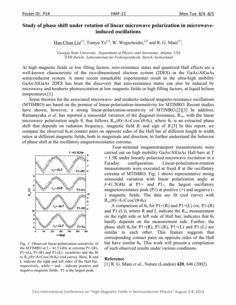
Poster ID: P14 HMF-‐21 Mon-‐Tue 8/4 -‐8/5
21st International Conference on "High Magnetic Fields in Semiconductor Physics" August 3-‐8, 2014
Fig. 1: Observed linear-polarization-sensitivity of the MTIMRO at f = 41.5 GHz at extrema P1+(R), P1+(L), P1-(R) and P1-(L) (symbols) and the fit to Rxx(θ)=A±Ccos2(θ-θ0) (red curve). Here, R and L indicate the right and left sides of the Hall bar, respectively, while + and – indicate positive and negative magnetic fields. P1 is the largest peak.
Study of phase shift under rotation of linear microwave polarization in microwave-induced oscillations
Han-Chun Liu(1), Tianyu Ye(1), W. Wegscheider,(2) and R. G. Mani(1),
1Georgia State University, Department of Physics and Astronomy, Atlanta, USA
2ETH Zurich, Laboratorium fur Feskorperphysik, Zurich, Switzerland At high magnetic fields or low filling factors, zero-resistance states and quantized Hall effects are a well-known characteristic of the two-dimensional electron system (2DES) in the GaAs/AlGaAs semiconductor system. A more recent remarkable experimental result in the ultra-high mobility GaAs/AlGaAs 2DES has been the discovery that zero-resistance states can also be induced by microwave and terahertz photoexcitation at low magnetic fields or high filling factors, at liquid helium temperatures.[1]
Some theories for the associated microwave- and terahertz-induced magneto-resistance oscillations (MTIMRO) are based on the premise of linear-polarization-insensitivity for MTIMRO. Recent studies have shown, however, a strong linear-polarization-sensitivity of MTIMRO.[2][3] In addition, Ramanayaka et al. has reported a sinusoidal variation of the diagonal resistance, Rxx, with the linear microwave polarization angle θ, that follows Rxx(θ)=A±Ccos2(θ-θ0), where θ0 is an extracted phase shift that depends on radiation frequency, magnetic field B, and sign of B.[3] In this report, we compare the observed θ0 at contact pairs on opposite sides of the Hall bar of different length to width ratios at different magnetic fields, both in magnitude and direction, to further understand the behavior of phase shift at the oscillatory magnetoresistance extrema.
Four-terminal magnetotransport measurements were carried out on high mobility GaAs/AlGaAs Hall bars at T = 1.5K under linearly polarized microwave excitation in a Faraday configuration. Linear-polarization-rotation measurements were executed at fixed B at the oscillatory extrema of MTIMRO. Fig. 1 shows representative strong sinusoidal variation with linear polarization angle at f=41.5GHz at P1+ and P1-, the largest oscillatory magnetoresistance peak (P1) at positive (+) and negative (-) magnetic fields. The data are fit (red curve) with Rxx(θ)=A±Ccos2(θ-θ0). A comparison of θ0 for P1+(R) and P1+(L) (or, P1-(R) and P1-(L)), where R and L indicate the Rxx measurement on the right side or left side of Hall bar, indicates that θ0 hardly depends on the measurement side. Further, the phase shift θ0 for P1+(R), P1-(R), P1+(L) and P1-(L) are similar to each other. This feature suggests that corresponding contact pairs on opposite sides of the Hall bar have similar θ0. This work will present a compilation of such observed results under various conditions. Reference [1] R. G. Mani et al., Nature (London) 420, 646 (2002).
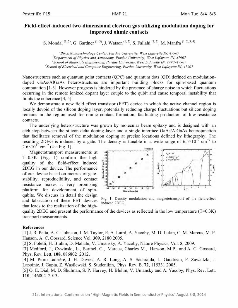
Poster ID: P15 HMF-‐21 Mon-‐Tue 8/4 -‐8/5
21st International Conference on "High Magnetic Fields in Semiconductor Physics" August 3-‐8, 2014
Field-effect-induced two-dimensional electron gas utilizing modulation doping for improved ohmic contacts
S. Mondal (1, 2), G. Gardner (1, 3), J. Watson (1, 2), S. Fallahi (1, 2), M. Manfra (1, 2, 3, 4)
1Birck Nanotechnology Center, Purdue University, West Lafayette IN, 47907
2Department of Physics and Astronomy, Purdue University, West Lafayette IN, 47907 3School of Materials Engineering, Purdue University, West Lafayette IN, 4790747907
4School of Electrical and Computer Engineering, Purdue University, West Lafayette IN, 47907
Nanostructures such as quantum point contacts (QPC) and quantum dots (QD) defined on modulation-doped GaAs/AlGaAs heterostructures are important building blocks for spin-based quantum computation [1-3]. However progress is hindered by the presence of charge noise in which fluctuations occurring in the remote ionized dopant layer couple to the qubit and cause temporal instability that limits the coherence [4, 5].
We demonstrate a new field effect transistor (FET) device in which the active channel region is locally devoid of the silicon doping layer, potentially reducing charge fluctuations but silicon doping remains in the region used for ohmic contact formation, facilitating production of low-resistance contacts.
The underlying heterostructure was grown by molecular beam epitaxy and is designed with an etch-stop between the silicon delta-doping layer and a single-interface GaAs/AlGaAs heterojunction that facilitates removal of the modulation doping at precise locations defined by lithography. The resulting 2DEG is induced by a gate. The density is tunable in a wide range of 6.5×1010 cm−2 to 2.6×1011 cm−2 (see Fig. 1).
Magnetotransport measurements at T=0.3K (Fig. 1) confirm the high quality of the field-effect induced 2DEG in our device. The performance of our device based on metrics of gate-stability, reproducibility, and contact resistance makes it very promising platform for development of spin-qubits. We discuss in detail the design and fabrication of these FET devices that leads to the realization of the high-quality 2DEG and present the performance of the devices as reflected in the low temperature (T=0.3K) transport measurements. References [1] J. R. Petta, A. C. Johnson, J. M. Taylor, E. A. Laird, A. Yacoby, M. D. Lukin, C. M. Marcus, M. P. Hanson, A. C. Gossard, Science Vol. 309, 2180 2005. [2] S. Foletti, H. Bluhm, D. Mahalu, V. Umansky, A. Yacoby, Nature Physics, Vol. 5, 2009. [3] Medford, J., Cywinski, L., Barthel, C., Marcus, Charles M., Hanson, M.P., and A. C. Gossard, Phys. Rev. Lett. 108, 086802 2012. [4] M. Pioro-Ladrière, J. H. Davies, A. R. Long, A. S. Sachrajda, L. Gaudreau, P. Zawadzki, J. Lapointe, J. Gupta, Z. Wasilewski, S. Studenikin, Phys. Rev. B. 72, 115331 2005. [5] O. E. Dial, M. D. Shulman, S. P. Harvey, H. Bluhm, V. Umansky and A. Yacoby, Phys. Rev. Lett. 110, 146804 2013.
Fig. 1: Density modulation and magnetotransport of the field-effect induced 2DEG.
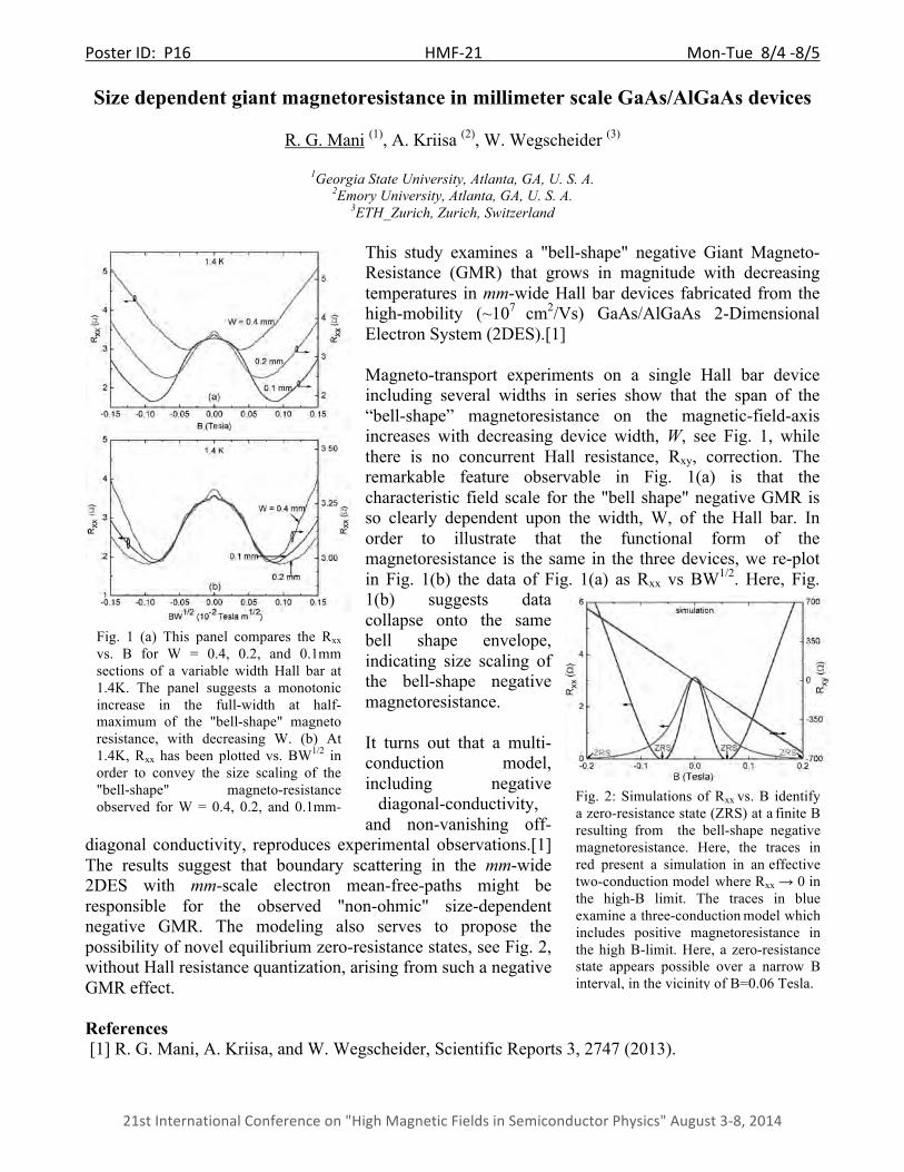
Poster ID: P16 HMF-‐21 Mon-‐Tue 8/4 -‐8/5
21st International Conference on "High Magnetic Fields in Semiconductor Physics" August 3-‐8, 2014
Size dependent giant magnetoresistance in millimeter scale GaAs/AlGaAs devices
R. G. Mani (1), A. Kriisa (2), W. Wegscheider (3)
1Georgia State University, Atlanta, GA, U. S. A. 2Emory University, Atlanta, GA, U. S. A.
3ETH_Zurich, Zurich, Switzerland
This study examines a "bell-shape" negative Giant Magneto-Resistance (GMR) that grows in magnitude with decreasing temperatures in mm-wide Hall bar devices fabricated from the high-mobility (~107 cm2/Vs) GaAs/AlGaAs 2-Dimensional Electron System (2DES).[1] Magneto-transport experiments on a single Hall bar device including several widths in series show that the span of the “bell-shape” magnetoresistance on the magnetic-field-axis increases with decreasing device width, W, see Fig. 1, while there is no concurrent Hall resistance, Rxy, correction. The remarkable feature observable in Fig. 1(a) is that the characteristic field scale for the "bell shape" negative GMR is so clearly dependent upon the width, W, of the Hall bar. In order to illustrate that the functional form of the magnetoresistance is the same in the three devices, we re-plot in Fig. 1(b) the data of Fig. 1(a) as Rxx vs BW1/2. Here, Fig. 1(b) suggests data collapse onto the same bell shape envelope, indicating size scaling of the bell-shape negative magnetoresistance. It turns out that a multi-conduction model, including negative
diagonal-conductivity, and non-vanishing off-
diagonal conductivity, reproduces experimental observations.[1] The results suggest that boundary scattering in the mm-wide 2DES with mm-scale electron mean-free-paths might be responsible for the observed "non-ohmic" size-dependent negative GMR. The modeling also serves to propose the possibility of novel equilibrium zero-resistance states, see Fig. 2, without Hall resistance quantization, arising from such a negative GMR effect. References [1] R. G. Mani, A. Kriisa, and W. Wegscheider, Scientific Reports 3, 2747 (2013).
Fig. 1 (a) This panel compares the Rxx vs. B for W = 0.4, 0.2, and 0.1mm sections of a variable width Hall bar at 1.4K. The panel suggests a monotonic increase in the full-width at half-maximum of the "bell-shape" magneto resistance, with decreasing W. (b) At 1.4K, Rxx has been plotted vs. BW1/2 in order to convey the size scaling of the "bell-shape" magneto-resistance observed for W = 0.4, 0.2, and 0.1mm-wide Hall bars.
Fig. 2: Simulations of Rxx vs. B identify a zero-resistance state (ZRS) at a finite B resulting from the bell-shape negative magnetoresistance. Here, the traces in red present a simulation in an effective two-conduction model where Rxx → 0 in the high-B limit. The traces in blue examine a three-conduction model which includes positive magnetoresistance in the high B-limit. Here, a zero-resistance state appears possible over a narrow B interval, in the vicinity of B=0.06 Tesla.
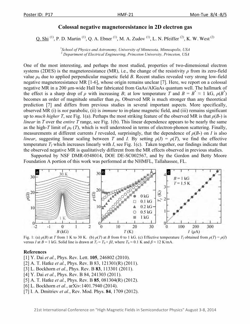
Poster ID: P17 HMF-‐21 Mon-‐Tue 8/4 -‐8/5
21st International Conference on "High Magnetic Fields in Semiconductor Physics" August 3-‐8, 2014
Colossal negative magnetoresistance in 2D electron gas
Q. Shi (1), P. D. Martin (1), Q. A. Ebner (1), M. A. Zudov (1), L. N. Pfeiffer (2), K. W. West (2)
1School of Physics and Astronomy, University of Minnesota, Minneapolis, USA 2 Department of Electrical Engineering, Princeton University, Princeton, USA
One of the most interesting, and perhaps the most studied, properties of two-dimensional electron systems (2DES) is the magnetoresistance (MR), i.e., the change of the resistivity ρ from its zero-field value ρ0 due to applied perpendicular magnetic field B. Recent studies revealed very strong low-field negative magnetoresistance MR [1-6], whose origin remains unclear [7]. Here, we report on a colossal negative MR in a 200 µm-wide Hall bar fabricated from GaAs/AlGaAs quantum well. The hallmark of the effect is a sharp drop of ρ with increasing B; at low temperature T and B = B* ≈ 1 kG, ρ(B*) becomes an order of magnitude smaller than ρ0. Observed MR is much stronger than any theoretical prediction [7] and differs from previous studies in several important aspects. More specifically, observed MR (i) is not parabolic, (ii) is immune to in-plane magnetic field, and (iii) remains significant up to much higher T, see Fig. 1(a). Perhaps the most striking feature of the observed MR is that ρ(B*) is linear in T over the entire T range, see Fig. 1(b). This linear dependence appears to be nearly the same as the high-T limit of ρ0 (T), which is well understood in terms of electron-phonon scattering. Finally, measurements at different currents I revealed, surprisingly, that the dependence of ρ(B*) on I is also linear, suggesting linear scaling between T and I. By setting ρ(I) = ρ(T), we find the effective temperature TI which increases linearly with I, see Fig. 1(c). Taken together, our findings indicate that the observed negative MR is qualitatively different from the MR effects observed in previous studies.
Supported by NSF DMR-0548014, DOE DE-SC002567, and by the Gordon and Betty Moore Foundation A portion of this work was performed at the NHMFL, Tallahassee, FL.
Fig. 1: (a) ρ(B) at T from 1 K to 30 K. (b) ρ(T) at B from 0 to 1 kG. (c) Effective temperature TI obtained from ρ(T) = ρ(I) versus I at B = 1 kG. Solid line is drawn at TI = T0 + βI, where T0 ≈ 0.1 K and β ≈ 12 K/mA. References [1] Y. Dai et al., Phys. Rev. Lett. 105, 246802 (2010). [2] A. T. Hatke et al., Phys. Rev. B 83, 121301(R) (2011). [3] L. Bockhorn et al., Phys. Rev. B 83, 113301 (2011). [4] Y. Dai et al., Phys. Rev. B 84, 241303 (2011). [5] A. T. Hatke et al., Phys. Rev. B 85, 081304(R) (2012). [6] L. Bockhorn et al., arXiv:1401.7940 (2014). [7] I. A. Dmitriev et al., Rev. Mod. Phys. 84, 1709 (2012).
Poster ID: P18 HMF-‐21 Mon-‐Tue 8/4 -‐8/5
21st International Conference on "High Magnetic Fields in Semiconductor Physics" August 3-‐8, 2014
Physical properties of single crystal graphite under pulsed magnetic fields up to 75 T
K. Akiba (1), A. Miyake (1), H. Yaguchi (2), A. Matsuo (1), K. Kindo (1), Y. Iye (1), M. Tokunaga (1)
1Institute for Solid State Physics, University of Tokyo/ Kashiwa, Chiba, Japan
2Tokyo University of Science/ Department of Physics, Faculty of Science and Technology, Noda, Chiba, Japan
Graphite consists of stacked graphene layers along the c-axis and is known as a typical semimetal. Application of high magnetic fields along the c-axis realizes the quasi quantum limit state that only four Landau sub-bands cross the Fermi surface. Further application of magnetic fields to this quasi quantum limit state causes abrupt increase in the in-plane and out-of-plane resistance between 25 T and 53 T [1] [2] [3]. Although this high-field state has been interpreted as a density wave state [4] [5], its true nature remains unclear. In addition, Fauque et al. recently revealed the existence of another peak in the out-of-plane magneto-resistance in the field region between 53 T and 75 T [6], and proposed possible edge state conduction that is characteristic of the quantum Hall state. Therefore, in-depth study on the high field state is highly desirable.
We investigated transport and magnetic properties of single crystal graphites with using non-destructive pulse magnets to clarify the intrinsic properties of graphite. Since the superficial transport properties are sensitive to the extrinsic factors in highly anisotropic conductors like graphite, we paid much attention to the geometrical configurations and possible deformations of the crystals. We discuss the intrinsic properties in the field-induced states of graphite with showing the results of high-field magnetization, transverse/longitudinal magneto-resistance, and Hall resistance.
References [1] S. Tanuma et al., :Physics in High Magnetic Fields, ed. S. Chikazumi and N. Miura (Springer, Berlin 1981) p.316. [2] H. Yaguchi et al., J. Phys. Soc. Jpn. 68,181 (1999). [3] H. Yaguchi and J. Singleton, J. Phys.: Condens. Matter 21, 344207 (2009). [4] D. Yoshioka and H. Fukuyama, J. Phys. Soc. Jpn. 50, 725 (1981). [5] Y. Takada and H. Goto, J. Phys.: Condens. Matter 10, 11315 (1998). [6] B. Fauque et al., Phys. Lev. Lett. 110, 266601 (2013).
Poster ID: P19 HMF-‐21 Mon-‐Tue 8/4 -‐8/5
21st International Conference on "High Magnetic Fields in Semiconductor Physics" August 3-‐8, 2014
Electrical transport in indium-decorated graphene sheets
Erik A. Henriksen (1), Chandni U (2), J.P. Eisenstein (2)
1Washington University in St. Louis, St. Louis, MO 63130, USA
2California Institute of Technology, Pasadena, CA 91125, USA Heavy adatoms on graphene are expected to alter its intrinsic properties in many novel ways. Here we report magneto-transport measurements on single layer graphene sheets which have been decorated with dilute concentrations of indium adatoms. These measurements are made using a custom-built evaporator housed in an ultra-high vacuum cryostat. This apparatus allows for the annealing of the graphene sample, the controlled deposition and removal of the In adatoms, and the actual transport measurements to all be done in situ. As expected, we find the In adatoms donate electrons to the graphene sheet, thereby shifting the location of the Dirac peak. More interestingly, our measurements clearly reveal how the In adatoms influence the scattering environment experienced by the Dirac electrons. Beyond merely reducing the sample mobility via enhanced charged impurity scattering, we find that the indium adatoms alter the “puddle” landscape near the Dirac point and modify the low field magneto-resistance signatures of weak localization and anti-localization.
Poster ID: P20 HMF-‐21 Mon-‐Tue 8/4 -‐8/5
21st International Conference on "High Magnetic Fields in Semiconductor Physics" August 3-‐8, 2014
Two-phonon scattering in graphene in the quantum Hall regime
A. M. Alexeev and M. E. Portnoi
School of Physics, University of Exeter, Exeter, United Kingdom
One of the most distinctive features of graphene is its huge inter-Landau-level splitting in experimentally attainable magnetic fields resulting in the room-temperature quantum Hall effect. We have calculated the longitudinal conductivity due to two-phonon scattering in graphene in a quantizing magnetic field over a broad range of temperatures. The multi-phonon scattering mechanism [1] is known to be negligible for conventional two-dimensional systems under the quantum Hall conditions apart from exotic cases such as magneto-roton dissociation in phonon spectroscopy [2]. However, our calculations show that this mechanism dominates in the high-temperature quantum Hall regime in graphene, since at elevated temperatures the energy of an acoustic phonon with a wavevector comparable to the inverse magnetic length is much smaller than the temperature; therefore, a number of such phonons increases drastically. Single-phonon processes in pristine graphene in this regime remain suppressed due to momentum and energy conservation requirements. We show that the two-phonon scattering mechanism provides a significant error in Hall conductivity measurements, and it is therefore a major obstacle in using graphene as a room-temperature quantum Hall standard of resistance.
References [1] V. N. Golovach and M. E. Portnoi, Phys. Rev. B 74, 085321 (2006). [2] V. M. Apalkov and M. E. Portnoi, Phys. Rev. B 66, 121303 (2002).
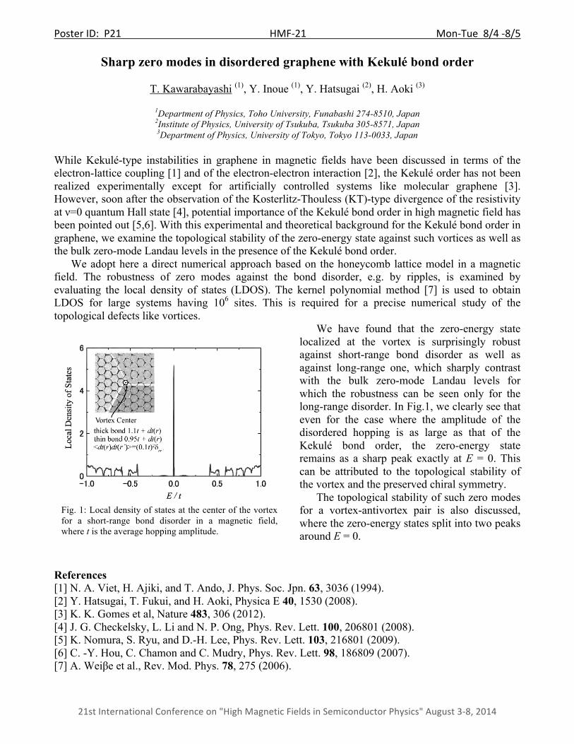
Poster ID: P21 HMF-‐21 Mon-‐Tue 8/4 -‐8/5
21st International Conference on "High Magnetic Fields in Semiconductor Physics" August 3-‐8, 2014
Sharp zero modes in disordered graphene with Kekulé bond order
T. Kawarabayashi (1), Y. Inoue (1), Y. Hatsugai (2), H. Aoki (3)
1Department of Physics, Toho University, Funabashi 274-8510, Japan 2Institute of Physics, University of Tsukuba, Tsukuba 305-8571, Japan 3Department of Physics, University of Tokyo, Tokyo 113-0033, Japan
While Kekulé-type instabilities in graphene in magnetic fields have been discussed in terms of the electron-lattice coupling [1] and of the electron-electron interaction [2], the Kekulé order has not been realized experimentally except for artificially controlled systems like molecular graphene [3]. However, soon after the observation of the Kosterlitz-Thouless (KT)-type divergence of the resistivity at ν=0 quantum Hall state [4], potential importance of the Kekulé bond order in high magnetic field has been pointed out [5,6]. With this experimental and theoretical background for the Kekulé bond order in graphene, we examine the topological stability of the zero-energy state against such vortices as well as the bulk zero-mode Landau levels in the presence of the Kekulé bond order. We adopt here a direct numerical approach based on the honeycomb lattice model in a magnetic field. The robustness of zero modes against the bond disorder, e.g. by ripples, is examined by evaluating the local density of states (LDOS). The kernel polynomial method [7] is used to obtain LDOS for large systems having 106 sites. This is required for a precise numerical study of the topological defects like vortices.
We have found that the zero-energy state localized at the vortex is surprisingly robust against short-range bond disorder as well as against long-range one, which sharply contrast with the bulk zero-mode Landau levels for which the robustness can be seen only for the long-range disorder. In Fig.1, we clearly see that even for the case where the amplitude of the disordered hopping is as large as that of the Kekulé bond order, the zero-energy state remains as a sharp peak exactly at E = 0. This can be attributed to the topological stability of the vortex and the preserved chiral symmetry. The topological stability of such zero modes for a vortex-antivortex pair is also discussed, where the zero-energy states split into two peaks around E = 0.
References [1] N. A. Viet, H. Ajiki, and T. Ando, J. Phys. Soc. Jpn. 63, 3036 (1994). [2] Y. Hatsugai, T. Fukui, and H. Aoki, Physica E 40, 1530 (2008). [3] K. K. Gomes et al, Nature 483, 306 (2012). [4] J. G. Checkelsky, L. Li and N. P. Ong, Phys. Rev. Lett. 100, 206801 (2008). [5] K. Nomura, S. Ryu, and D.-H. Lee, Phys. Rev. Lett. 103, 216801 (2009). [6] C. -Y. Hou, C. Chamon and C. Mudry, Phys. Rev. Lett. 98, 186809 (2007). [7] A. Weiβe et al., Rev. Mod. Phys. 78, 275 (2006).
Fig. 1: Local density of states at the center of the vortex for a short-range bond disorder in a magnetic field, where t is the average hopping amplitude.

Poster ID: P22 HMF-‐21 Mon-‐Tue 8/4 -‐8/5
21st International Conference on "High Magnetic Fields in Semiconductor Physics" August 3-‐8, 2014
Hot-Carrier Relaxation in Graphene in a Quantizing Magnetic Field
H. Ramamoorthy1, R. Somphonsane2, D. K. Ferry3, and J. P. Bird1
1 Department of Electrical Engineering, University at Buffalo, Buffalo, NY, USA
2Department of Physics, King Mongkut’s Institute of Technology Ladkrabang, Bangkok, Thailand 3 School of Electrical, Computer, and Energy Engineering, and Center for Solid State
Electronics Research, Arizona State University, Tempe, AZ, USA
With the emergence of graphene as a promising new material for nanoelectronics, the need to understand the energy relaxation of its hot carriers is critical to the realization of future devices based on this material. The importance of this problem is driving ongoing theoretical and experimental activity, and we have recently shown [1] that the energy-relaxation rate for hot carriers in graphene increases significantly as the Dirac point is approached from either the conduction or valence band. Although unexpected from simple density-of-states arguments, we have suggested that this behavior may be consistent with the known strong incompressibility of electron-hole puddles that form near the Dirac point.
Building on our prior work, here we study how the energy relaxation of hot carriers in graphene is modified by the presence of a magnetic field. By utilizing quantum-transport thermometry to determine the energy-relaxation time [1], our analysis shows that the magnetic field causes a systematic slowing of energy relaxation, for electron and holes densities away from the Dirac point (see Fig. 1). In marked contrast to this, the energy-relaxation time is found to decrease near the Dirac point, indicating that energy loss proceeds more quickly when the magnetic field is applied (also see Fig. 1). Near the Dirac point at least, such behavior appears consistent with the expected influence of the magnetic field on the density of states, which should increase significantly with the applied field. Away from the Dirac point, however, the interpretation is less clear, since one expects regions of electron and
hole density for which the density of states should be significantly increased due to Landau-level formation. The increased cooling rate near the Dirac Point may therefore be connected to the physics of the “puddle state” itself, rather than involving a simple density-of-states interpretation. These ideas will be discussed in detail in our presentation. References [1] R. Somphonsane, H. Ramamoorthy, G. Bohra, G. He, D. K. Ferry, Y. Ochiai, N. Aoki, and J. P. Bird, "Fast energy relaxation of hot carriers near the Dirac point of graphene", Nano Lett. 13, 4305 (2013).
1.5 V, 6.5 V, 16.5 V, 26.5 V, 31.5 V, 36.5 V�
ELECTRON SIDE�
HOLE SIDE�
1.5 V, -3.5 V, -13.5 V, -23.5 V, -28.5 V�
Fig. 1: Measured variation of the energy relaxation time as a function of applied magnetic field. Systematic slowing of the relaxation dynamics is observed away from the Dirac Point (1.5 V) whereas the opposite trend is observed when the Dirac point is approached (note the logarithmic vertical scale).
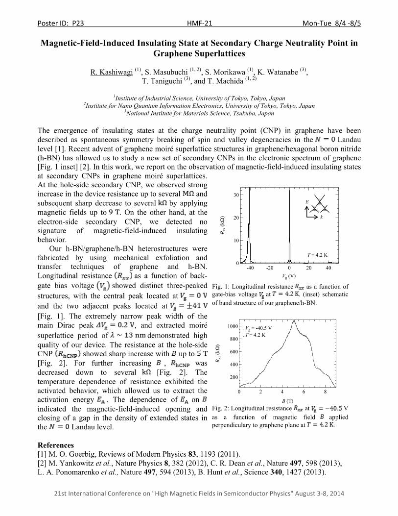
Poster ID: P23 HMF-‐21 Mon-‐Tue 8/4 -‐8/5
21st International Conference on "High Magnetic Fields in Semiconductor Physics" August 3-‐8, 2014
Magnetic-Field-Induced Insulating State at Secondary Charge Neutrality Point in Graphene Superlattices
R. Kashiwagi (1), S. Masubuchi (1, 2), S. Morikawa (1), K. Watanabe (3),
T. Taniguchi (3), and T. Machida (1, 2)
1Institute of Industrial Science, University of Tokyo, Tokyo, Japan 2Institute for Nano Quantum Information Electronics, University of Tokyo, Tokyo, Japan
3National Institute for Materials Science, Tsukuba, Japan The emergence of insulating states at the charge neutrality point (CNP) in graphene have been described as spontaneous symmetry breaking of spin and valley degeneracies in the Landau level [1]. Recent advent of graphene moiré superlattice structures in graphene/hexagonal boron nitride (h-BN) has allowed us to study a new set of secondary CNPs in the electronic spectrum of graphene [Fig. 1 inset] [2]. In this work, we report on the observation of magnetic-field-induced insulating states at secondary CNPs in graphene moiré superlattices. At the hole-side secondary CNP, we observed strong increase in the device resistance up to several and subsequent sharp decrease to several by applying magnetic fields up to . On the other hand, at the electron-side secondary CNP, we detected no signature of magnetic-field-induced insulating behavior.
Our h-BN/graphene/h-BN heterostructures were fabricated by using mechanical exfoliation and transfer techniques of graphene and h-BN. Longitudinal resistance as a function of back-gate bias voltage showed distinct three-peaked structures, with the central peak located at and the two adjacent peaks located at [Fig. 1]. The extremely narrow peak width of the main Dirac peak , and extracted moiré superlattice period of demonstrated high quality of our device. The resistance at the hole-side CNP showed sharp increase with up to [Fig. 2]. For further increasing , was decreased down to several [Fig. 2]. The temperature dependence of resistance exhibited the activated behavior, which allowed us to extract the activation energy . The dependence of on indicated the magnetic-field-induced opening and closing of a gap in the density of extended states in the Landau level. References [1] M. O. Goerbig, Reviews of Modern Physics 83, 1193 (2011). [2] M. Yankowitz et al., Nature Physics 8, 382 (2012), C. R. Dean et al., Nature 497, 598 (2013), L. A. Ponomarenko et al., Nature 497, 594 (2013), B. Hunt et al., Science 340, 1427 (2013).
Fig. 1: Longitudinal resistance as a function of gate-bias voltage at . (inset) schematic of band structure of our graphene/h-BN.
Fig. 2: Longitudinal resistance at V as a function of magnetic field applied perpendiculary to graphene plane at .

Poster ID: P24 HMF-‐21 Mon-‐Tue 8/4 -‐8/5
21st International Conference on "High Magnetic Fields in Semiconductor Physics" August 3-‐8, 2014
Electric Field Effects and Landau Level Crossing in Suspended Bilayer and Trilayer Graphene
K. Myhro, Y. Lee, M. Deo, D. Tran, C. N. Lau
University of California, Riverside / Department of Physics and Astronomy, Riverside, CA, USA
Bilayer (BLG) and trilayer graphene (TLG), with their ultra-high tensile strengths, offer robust two-dimensional materials for suspended electronic transport measurements which exhibit the Quantum Hall Effect, have gate-tunable band gaps (BLG and rhombohedral-stacked TLG), and are useful platforms to study the competition between single particle physics and electron-electron interactions[1,2,3]. Here, we report two-terminal differential conductance measurements at low temperatures of dual-gated suspended BLG and TLG devices as a function of applied back gate and top gate voltages in zero and high magnetic fields. Multi-level electron beam lithography defines contactless top gates and the mechanically-exfoliated graphene flakes are suspended by wet-etching the oxide substrate layer using a buffered oxide etch[4]. Suspending few-layer graphene has proven to be a useful tool to achieve high mobility devices by reducing scattering effects by substrates. Successful current annealing of suspended BLG and TLG membranes allows us to reach this high mobility and an insulating state at low magnetic fields.
The use of a suspended, contactless top gate allows us to independently control the charge carrier density and perpendicular electric field in suspended devices, which is critical to study electronic interactions and Landau Level crossings. We investigate the role of the applied perpendicular electric field from top-gated devices, compare results to single-gated measurements, and characterize Landau Level crossings in BLG and TLG as a function of electric field, charge carrier density and magnetic field.
References [1] Y. Zhang, et al., Nature Phys. 459, 820-823 (2009). [2] C. H. Lui, et al., Nature, 7, 944-947 (2011). [3] J. Velasco Jr., et al., Nature Nanotech. 7, 156-160 (2012). [4] G. Liu, et al., Appl. Phys. Lett. 92, 203103 (2008).
Fig. 1: Figures (grayscale preferable) and tables should be positioned appropriately on the page. Captions should be printed in single line spacing, Times Roman family 10pt.
Fig. 1: Two-terminal differential conductance (dI/dV) of a bilayer graphene device vs. perpendicular Electric field and charge carrier density. Line traces (right) are taken at finite charge carrier density and show evidence of Landau Level crossings.
Poster ID: P25 HMF-‐21 Mon-‐Tue 8/4 -‐8/5
21st International Conference on "High Magnetic Fields in Semiconductor Physics" August 3-‐8, 2014
Magnetic field induced confinement-deconfinement transitions in Dirac materials
C. A. Downing (1), K. S. Gupta (2), M. E. Portnoi (1)
1School of Physics, University of Exeter, Exeter, United Kingdom 2 Theory Division, Saha Institute of Nuclear Physics, Calcutta, India
There is a widespread belief that electrostatic confinement of graphene charge carriers, which resemble massless Dirac fermions, is impossible as a result of the Klein paradox [1]. We have shown previously that full confinement is indeed possible for zero-energy states in pristine graphene with careful modulation of the strength of the trapping electrostatic potential [2]. The addition of a magnetic flux tube to the system requires one to perform a one-parameter self-adjoint extension of the Dirac Hamiltonian to completely define the spectrum of the zero-modes, which can be carried out using the method of deficiency indices developed by von Neumann [3]. We propose such a magnetic vector potential as an additional means to control these optimal quantum dots supporting zero-energy states and bring about confinement-deconfinement on demand [4]. The considered system can be utilized in novel graphene-based magnetic read-out devices.
We also revisit the problem of trapping of Dirac-Weyl particles in magnetic quantum dots and rings, showing how it is indeed possible to confine such quasi-relativistic particles. Earlier toy models, which considered less realistic dots and rings which were sharply defined in space, suggested only confinement in magnetic antidots (zero magnetic field inside a region of finite magnetic field) was possible [5]. However we show here, with more realistic models describing spatially smooth dots and rings, as long as the spatial decay at infinity of the magnetic field is slower than the inverse square of the radial distance, fully bound modes may form. Our work is based on both exact and hitherto unknown quasi-exact solutions [6]. It is also found that one sign of the electron angular momentum quantum number is excluded depending on the sign of the field. In graphene, mechanical strain can give rise to a pseudomagnetic field [7], where the sign of the effective magnetic field is opposite in the two valleys – such that states will rotate with positive angular momentum in one valley and with negative angular momentum in the other valley. Exploiting this phenomenon, a combination of a real magnetic field with pseudomagnetic fields generated by strain, could be useful in future mesoscopic devices.
References [1] M. I. Katsnelson, K. S. Novoselov, and A. K. Geim, Nature Phys. 2, 620 (2006). [2] C. A. Downing, D. A. Stone, and M. E. Portnoi, Phys. Rev. B 84, 155437 (2011). [3] M. Reed and B. Simon, Methods of Modern Mathematical Physics, (Academic Press, 1972). [4] C. A. Downing, K. S. Gupta and M. E. Portnoi, (in preparation, 2014). [5] A. De Martino, L. DellAnna, and R. Egger, Phys. Rev. Lett. 98, 066802 (2007). [6] A. V. Turbiner, Sov. Phys. JETP 67, 230 (1988). [7] F. Guinea, M. I. Katsnelson, and A. K. Geim, Nat. Phys. 6, 30 (2009).

Poster ID: P26 HMF-‐21 Mon-‐Tue 8/4 -‐8/5
21st International Conference on "High Magnetic Fields in Semiconductor Physics" August 3-‐8, 2014
Oscillatory inter-edge-channel mixing between counter-circulating quantum-Hall edge channels in graphene p-n junctions
Tomoki Machida (1,2), Sei Morikawa (1), Satoru Masubuchi (1,2), Rai Moriya (1),
Kenji Watanabe (3), Takashi Taniguchi (3)
1 Institute of Industrial Science, University of Tokyo, Tokyo 153-8505, Japan 2 INQIE, University of Tokyo, Tokyo 153-8505, Japan
3 National Institute for Materials Science, Ibaraki 305-0044, Japan
Edge-channel picture has been widely utilized to explain transport properties of quantum Hall systems. Especially, in graphene p-n junctions at high magnetic fields, the electron and hole modes of the quantum Hall edge channels can mix at the p-n intereface. The current partitioning due to the mixing of the channels leads to the observation of quantized Hall plateaus with R = h / e2( ) ⋅ νn ν p / νn + ν p( ) ,
where and denote the Landau-level filling factors in the n and p regions, respectively. In this work, we study carrier transmission between counter-circulating quantum Hall edge channels at p-n interfaces, where the electron and hole modes of the quantum Hall edge channels are not fully equilibrated. The high-mobility dual-gated h-BN/graphene/h-BN devices are fabricated using mechanical exfoliation and dry transfer techniques of graphene and h-BN. The carrier polarity and density in two adjacent regions are tuned with a pair of top and bottom gate electrodes. When the charge carrier configuration is n-n’-n, two-terminal magnetoresistance across the junctions exhibit conventional quantum Hall plateaus. On the other hand, the resistance across the n-p-n junctions exceeds quantum resistance of h/e2 and resistance oscillations emerge in intermediate magnetic-field ranges. The oscillation period does not scale with 1/B nor B, suggesting a novel oscillatory behavior in inter-edge-channel mixing between counter-circulating quantum Hall edge channels at the p-n interface. Our simulations based on the flux quantization in the area between the edge channels can reproduce the peak positions of the magnetoresisntace oscillations.
Fig. 1: Color-plot of two-terminal magnetoresistance of graphene n-n’-n (left) and n-p-n (center) junctions. Simulated peak positions of carrier transmission between the counter-circulating quantum Hall edge channels at the p-n interface (right).
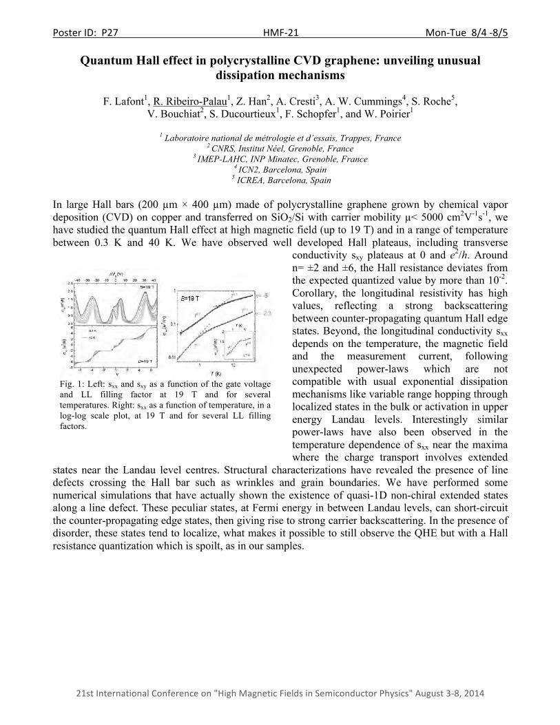
Poster ID: P27 HMF-‐21 Mon-‐Tue 8/4 -‐8/5
21st International Conference on "High Magnetic Fields in Semiconductor Physics" August 3-‐8, 2014
Quantum Hall effect in polycrystalline CVD graphene: unveiling unusual dissipation mechanisms
F. Lafont1, R. Ribeiro-Palau1, Z. Han2, A. Cresti3, A. W. Cummings4, S. Roche5,
V. Bouchiat2, S. Ducourtieux1, F. Schopfer1, and W. Poirier1
1 Laboratoire national de métrologie et d’essais, Trappes, France 2 CNRS, Institut Néel, Grenoble, France
3 IMEP-LAHC, INP Minatec, Grenoble, France 4 ICN2, Barcelona, Spain
5 ICREA, Barcelona, Spain In large Hall bars (200 µm × 400 µm) made of polycrystalline graphene grown by chemical vapor deposition (CVD) on copper and transferred on SiO2/Si with carrier mobility µ< 5000 cm2V-1s-1, we have studied the quantum Hall effect at high magnetic field (up to 19 T) and in a range of temperature between 0.3 K and 40 K. We have observed well developed Hall plateaus, including transverse
conductivity sxy plateaus at 0 and e2/h. Around n= ±2 and ±6, the Hall resistance deviates from the expected quantized value by more than 10-2. Corollary, the longitudinal resistivity has high values, reflecting a strong backscattering between counter-propagating quantum Hall edge states. Beyond, the longitudinal conductivity sxx depends on the temperature, the magnetic field and the measurement current, following unexpected power-laws which are not compatible with usual exponential dissipation mechanisms like variable range hopping through localized states in the bulk or activation in upper energy Landau levels. Interestingly similar power-laws have also been observed in the temperature dependence of sxx near the maxima where the charge transport involves extended
states near the Landau level centres. Structural characterizations have revealed the presence of line defects crossing the Hall bar such as wrinkles and grain boundaries. We have performed some numerical simulations that have actually shown the existence of quasi-1D non-chiral extended states along a line defect. These peculiar states, at Fermi energy in between Landau levels, can short-circuit the counter-propagating edge states, then giving rise to strong carrier backscattering. In the presence of disorder, these states tend to localize, what makes it possible to still observe the QHE but with a Hall resistance quantization which is spoilt, as in our samples.
Fig. 1: Left: sxx and sxy as a function of the gate voltage and LL filling factor at 19 T and for several temperatures. Right: sxx as a function of temperature, in a log-log scale plot, at 19 T and for several LL filling factors.
Poster ID: P28 HMF-‐21 Mon-‐Tue 8/4 -‐8/5
21st International Conference on "High Magnetic Fields in Semiconductor Physics" August 3-‐8, 2014
Megagauss Cyclotron Resonances in Monolayer and Bilayer Graphene/SiC
S. Takeyama (1), H. Saito (2), T. Numata (2), D. Nakamura (1), and H. Hibino (3)
1The Institute for Solid State Physics, The UTokyo, Kashiwa, Japan 2Dep. of Appl. Phys., The UTokyo, Hongo,Tokyo, Japan
3NTT Basic Research Labs., NTT Corporation, Astugi, Japan Recent developments of the electro-magnetic flux compression technique enable us to perform cyclotron resonance measurements in extremely high magnetic fields approaching to 700 T. Well resolved CR peaks appeared at several hundreds Tesla in both the monolayer and bilayer graphene grown on a 4H-SiC substrate. In such high-fields the electron correlation energy, the inter-valley interaction energy, and also the Zeeman energy are expected to easily exceed the room temperature thermal energy. The CR transmission spectra were asymmetric and shown to model by Abergel’s formula[2]. The CR energies were found to obey the square-root B dependence even at 400 T for the case of monolayer graphene. Whereas, in bilayer graphene the highest resonance was around 450 T. The band gap energy as well as the valley splitting energy was obtained with good accuracy via fitting of the Landau fan-chart and the results were compared with those obtained by the angle-resolved photo-emission spectra conducted on the same sample. References [1] S. Takeyama and E. Kojima, J. Phys. D: Appl. Phys. 44, 425003 (2011). [2] D. S. L. Abergel and Vladimir I. Fal'ko, Phys. Rev. B 75, 155430 (2007).
Poster ID: P29 HMF-‐21 Mon-‐Tue 8/4 -‐8/5
21st International Conference on "High Magnetic Fields in Semiconductor Physics" August 3-‐8, 2014
The cyclotron resonance of p-type CVD graphene/CaF2 or ZnSe in ultra-high magnetic fields
T. Numata (1), H. Saito(1), D. Nakamura(1), K. Yagi(2), K. Hayashi(2), S. Sato(2), S. Takeyama(1)
1Institute for Solid State Physics, UTokyo, Kashiwa, Japan
2National Inst. of Advanced Industrial Sci.&Tech. (AIST), Tsukuba, Japan We present results of the optical transmission measurements as the cyclotron resonance (CR) in ultra-high magnetic fields. The single-turn coil method was used for generating magnetic fields up to 140 T. The observed transitions between LLs caused by monolayer (ML) graphene showed Landau level (LL) energies with a square root dependence of the magnetic field (B) that is specific to the Dirac relativistic electrons. Two kinds of ML graphene were used as samples transferred on CaF2 and ZnSe substrates after the growth by the CVD method with a 30 cm diameter large size. The resonance light were near-infrared 3.39, 5.5, and infrared 10.2 µm wavelengths. The discernible peak was observed in magnetic fields of up to 120 T as the hole CR. A splitting was observed at the peak of CR spectrum. Our interest lies on whether this splitting is a result induced by the effects of the electron correlation, or the inter-valley interaction, or spin or psudo-spin Zeeman in ultra-high magnetic field CR spectra. Another interesting features were notified as the substrate and also the transfer target size dependence of the Fermi velocity determined from the LL curvatures in magnetic fields.
Poster ID: P30 HMF-‐21 Mon-‐Tue 8/4 -‐8/5
21st International Conference on "High Magnetic Fields in Semiconductor Physics" August 3-‐8, 2014
Coherent broadband THz spectrometer using photomixers for solid-state spectroscopy at low temperatures and high magnetic fields
K. Thirunavukkuarasu (1)*, M. Langenbach (1), I. Cámara Mayorga (2), A. Roggenbuck (3),
A. Deninger (2), J. Hemberger (1), and M. Grüninger (1)
1University of Cologne, Cologne, Germany 2Max-Planck-Institute for Radioastronomy, Bonn, Germany
3TOPTICA photonics AG, Gräfelfing, 82166, Germany *Current affiliation: National High Magnetic Field Laboratory, Tallahassee, USA
We discuss the development of a continuous-wave THz spectrometer for solid-state spectroscopy at low temperatures as well as high magnetic fields. The spectrometer is based on the principle of THz generation using frequency mixing of two near-infrared distributed feedback diode lasers with frequency stabilization [1]. The laser beat is converted into THz radiation by a photomixer, which efficiently generates THz radiation from 60 GHz to 1.8 THz. The THz radiation is detected by a second photomixer via homodyne mixing of the THz signal and the laser beat. A fast phase modulation technique using fiber stretchers is used to determine the amplitude and the phase at a given frequency with excellent reliability [2]. Also, a photocurrent correction is implemented to account for the drifts in the THz intensity using the dc photocurrents measured at the photomixers [3]. The complex optical functions can then be evaluated from the full phase information of the THz beam, and a very high spectral resolution in the MHz range can be achieved. More recently, we have implemented a third laser which increases the phase accuracy by enabling a correction for phase drifts mainly caused by thermal fluctuations. Thus, the complex dielectric function can be determined very accurately with a very high frequency resolution. Furthermore, the performance of the photomixers at low temperatures down to 5 K and high magnetic fields up to 8 T has been tested extensively to integrate this spectrometer within a commercial magneto-cryostat for spectroscopic investigations. We use a compact face-to-face assembly where the photomixers are inserted directly in the core of a magneto-cryostat. To overcome the need for optical windows in the cryostat, the optical fibers are transferred through vacuum-tight feedthroughs into the variable-temperature insert (VTI). The VTI provides the temperature control and enables positioning of our measurement setup in the cryostat. Various aspects of the above-mentioned developments will be outlined. References [1] A. Roggenbuck, H. Schmitz, A. Deninger, I. Cámara Mayorga, J. Hemberger, R. Güsten, and M. Grüninger, New J. Phys., 12, 043017 (2010). [2] A. Roggenbuck, K. Thirunavukkuarasu, H. Schmitz, J. Marx, A. Deninger, I. Cámara Mayorga, R. Güsten, J. Hemberger, and M. Grüninger, J. Opt. Soc. Am. B, 29, 614 (2012). [3] A. Roggenbuck, M. Langenbach, K. Thirunavukkuarasu, H. Schmitz, A. Deninger, I. Cámara Mayorga, R. Güsten, J. Hemberger, and M. Grüninger, J. Opt. Soc. Am. B, 30, 1397 (2013).
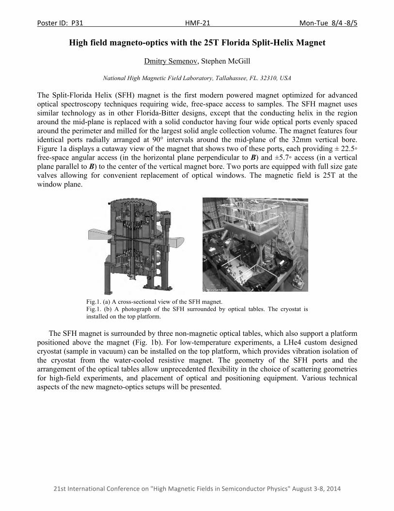
Poster ID: P31 HMF-‐21 Mon-‐Tue 8/4 -‐8/5
21st International Conference on "High Magnetic Fields in Semiconductor Physics" August 3-‐8, 2014
High field magneto-optics with the 25T Florida Split-Helix Magnet
Dmitry Semenov, Stephen McGill
National High Magnetic Field Laboratory, Tallahassee, FL. 32310, USA
The Split-Florida Helix (SFH) magnet is the first modern powered magnet optimized for advanced optical spectroscopy techniques requiring wide, free-space access to samples. The SFH magnet uses similar technology as in other Florida-Bitter designs, except that the conducting helix in the region around the mid-plane is replaced with a solid conductor having four wide optical ports evenly spaced around the perimeter and milled for the largest solid angle collection volume. The magnet features four identical ports radially arranged at 90° intervals around the mid-plane of the 32mm vertical bore. Figure 1a displays a cutaway view of the magnet that shows two of these ports, each providing ± 22.5◦ free-space angular access (in the horizontal plane perpendicular to B) and ±5.7◦ access (in a vertical plane parallel to B) to the center of the vertical magnet bore. Two ports are equipped with full size gate valves allowing for convenient replacement of optical windows. The magnetic field is 25T at the window plane.
The SFH magnet is surrounded by three non-magnetic optical tables, which also support a platform
positioned above the magnet (Fig. 1b). For low-temperature experiments, a LHe4 custom designed cryostat (sample in vacuum) can be installed on the top platform, which provides vibration isolation of the cryostat from the water-cooled resistive magnet. The geometry of the SFH ports and the arrangement of the optical tables allow unprecedented flexibility in the choice of scattering geometries for high-field experiments, and placement of optical and positioning equipment. Various technical aspects of the new magneto-optics setups will be presented.
Fig.1. (a) A cross-sectional view of the SFH magnet. Fig.1. (b) A photograph of the SFH surrounded by optical tables. The cryostat is installed on the top platform.
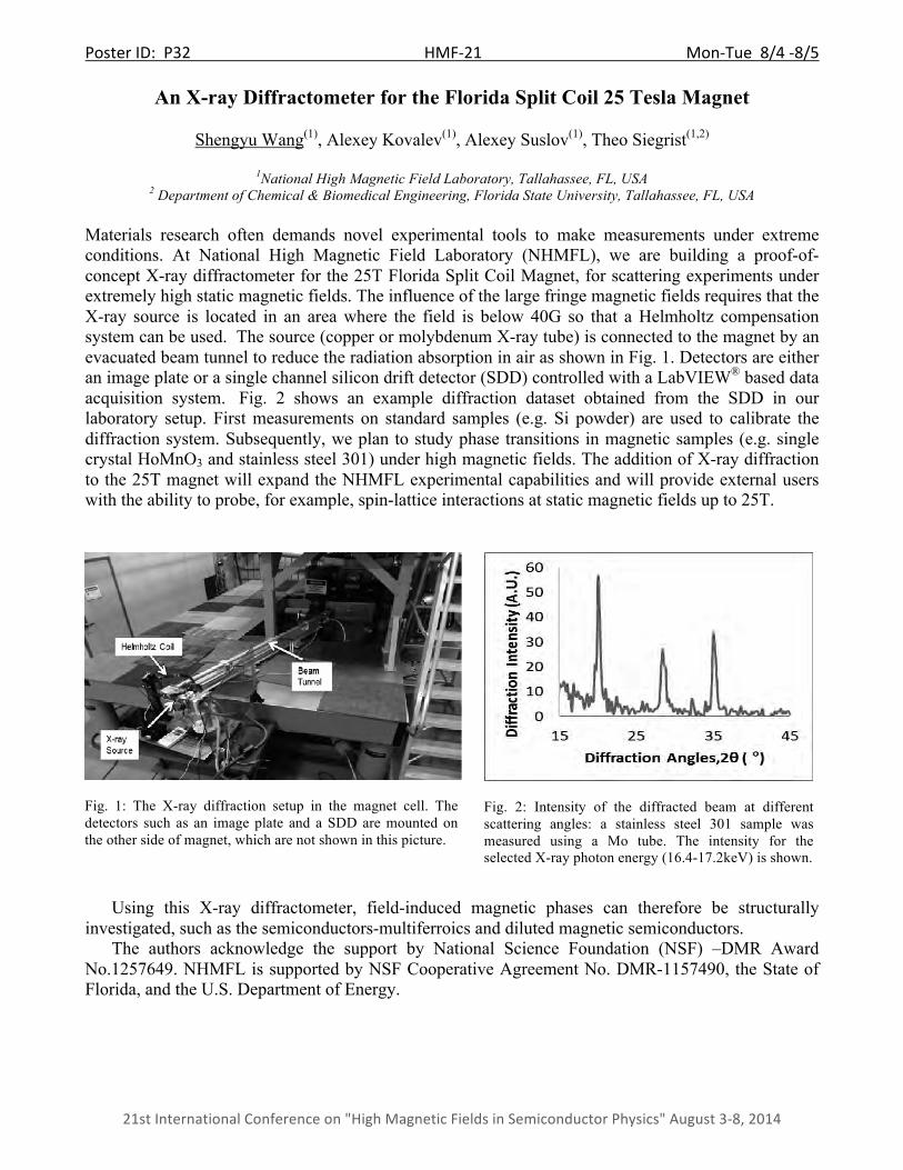
Poster ID: P32 HMF-‐21 Mon-‐Tue 8/4 -‐8/5
21st International Conference on "High Magnetic Fields in Semiconductor Physics" August 3-‐8, 2014
An X-ray Diffractometer for the Florida Split Coil 25 Tesla Magnet
Shengyu Wang(1), Alexey Kovalev(1), Alexey Suslov(1), Theo Siegrist(1,2)
1National High Magnetic Field Laboratory, Tallahassee, FL, USA 2 Department of Chemical & Biomedical Engineering, Florida State University, Tallahassee, FL, USA
Materials research often demands novel experimental tools to make measurements under extreme conditions. At National High Magnetic Field Laboratory (NHMFL), we are building a proof-of-concept X-ray diffractometer for the 25T Florida Split Coil Magnet, for scattering experiments under extremely high static magnetic fields. The influence of the large fringe magnetic fields requires that the X-ray source is located in an area where the field is below 40G so that a Helmholtz compensation system can be used. The source (copper or molybdenum X-ray tube) is connected to the magnet by an evacuated beam tunnel to reduce the radiation absorption in air as shown in Fig. 1. Detectors are either an image plate or a single channel silicon drift detector (SDD) controlled with a LabVIEW® based data acquisition system. Fig. 2 shows an example diffraction dataset obtained from the SDD in our laboratory setup. First measurements on standard samples (e.g. Si powder) are used to calibrate the diffraction system. Subsequently, we plan to study phase transitions in magnetic samples (e.g. single crystal HoMnO3 and stainless steel 301) under high magnetic fields. The addition of X-ray diffraction to the 25T magnet will expand the NHMFL experimental capabilities and will provide external users with the ability to probe, for example, spin-lattice interactions at static magnetic fields up to 25T.
Using this X-ray diffractometer, field-induced magnetic phases can therefore be structurally investigated, such as the semiconductors-multiferroics and diluted magnetic semiconductors.
The authors acknowledge the support by National Science Foundation (NSF) –DMR Award No.1257649. NHMFL is supported by NSF Cooperative Agreement No. DMR-1157490, the State of Florida, and the U.S. Department of Energy.
Fig. 1: The X-ray diffraction setup in the magnet cell. The detectors such as an image plate and a SDD are mounted on the other side of magnet, which are not shown in this picture.
Fig. 2: Intensity of the diffracted beam at different scattering angles: a stainless steel 301 sample was measured using a Mo tube. The intensity for the selected X-ray photon energy (16.4-17.2keV) is shown.
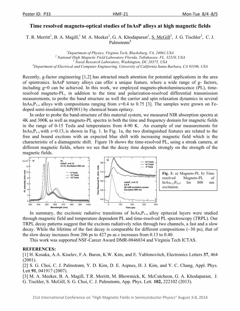
Poster ID: P33 HMF-‐21 Mon-‐Tue 8/4 -‐8/5
21st International Conference on "High Magnetic Fields in Semiconductor Physics" August 3-‐8, 2014
Time resolved magneto-optical studies of InAsP alloys at high magnetic fields
T. R. Merritt1, B. A. Magill,1 M. A. Meeker1, G. A. Khodaparast1, S. McGill2, J. G. Tischler3, C. J. Palmstrøm4
1Department of Physics, Virginia Tech, Blacksburg, VA, 24061,USA
2 National High Magnetic Field Laboratory Florida, Tallahassee, FL. 32310, USA 3 Naval Research Laboratory, Washington, DC 20375, USA
4Department of Electrical and Computer Engineering, University of California Santa Barbara, CA 93106, USA Recently, g-factor engineering [1,2] has attracted much attention for potential applications in the area of spintronics. InAsP ternary alloys can offer a unique feature, where a wide range of g- factors, including g=0 can be achieved. In this work, we employed magneto-photoluminescence (PL), time-resolved magneto-PL, in addition to the time and polarization-resolved differential transmission measurements, to probe the band structure as well the carrier and spin relaxation dynamics in several InAsxP1-x alloys with compositions ranging from x=0.4 to 0.75 [3]. The samples were grown on Fe-doped semi-insulating InP(001) by chemical beam epitaxy.
In order to probe the band-structure of this material system, we measured NIR absorption spectra at 4K and 300K as well as magneto-PL spectra in both the time and frequency domain for magnetic fields in the range of 0-15 Tesla and temperatures from 4-90 K. An example of our measurements for InAsxP1-x with x=0.13, is shown in Fig. 1. In Fig. 1a, the two distinguished features are related to the free and bound excitons with an expected blue shift with increasing magnetic field which is the characteristic of a diamagnetic shift. Figure 1b shows the time-resolved PL, using a streak camera, at different magnetic fields, where we see that the decay time depends strongly on the strength of the magnetic fields.
In summary, the excitonic radiative transitions of InAsxP1-x alloy epitaxial layers were studied
through magnetic field and temperature dependent PL and time-resolved PL spectroscopy (TRPL). Our TRPL decay patterns suggest that the excitons radiatively relax through two channels, a fast and a slow decay. While the lifetime of the fast decay is comparable for different compositions (~30 ps), that of the slow decay increases from 206 ps to 427 ps as x increases from 0.13 to 0.40.
This work was supported NSF-Career Award DMR-0846834 and Virginia Tech ICTAS. REFERENCES: [1] H. Kosaka, A.A. Kiselev, F.A. Baron, K.W. Kim, and E. Yablonovitch, Electronics Letters 37, 464 (2001). [2] S. G. Choi, C. J. Palmstrøm, Y. D. Kim, D. E. Aspnes, H. J. Kim, and Y. C. Chang, Appl. Phys. Lett 91, 041917 (2007). [3] M. A. Meeker, B. A. Magill, T.R. Merritt, M. Bhowmick, K. McCutcheon, G. A. Khodaparast, J. G. Tischler, S. McGill, S. G. Choi, C. J. Palmstrøm, App. Phys. Lett. 102, 222102 (2013).
Fig. 1: a) Magneto-PL b) Time resolved Magneto-PL of InAs0.13P0.67 for 800 nm excitation.
Poster ID: P34 HMF-‐21 Mon-‐Tue 8/4 -‐8/5
21st International Conference on "High Magnetic Fields in Semiconductor Physics" August 3-‐8, 2014
Magnetic field induced lattice deformation in the SrCu2(BO3)2 observed via Raman spectroscopy
J. G. Cherian (1, 2), T. D. Tokumoto (2), Y. Kim (1, 2), H. Zhou (2), D. Smirnov(2), S. A. McGill (2)
1Dept. of Physics, Florida State University, Tallahassee, USA 2National High Magnetic Field Laboratory, Tallahassee, USA
We report the magnetic field dependence (up to 45 T) of Raman spectra at 1.2 K in SrCu2(BO3)2, or SCBO, which is a highly-frustrated, low-dimensional quantum spin dimer system having a singlet ground state separated from the excited triplet state by an energy gap (∼35 K) that can be closed by high magnetic fields (>20 T). Dimer interactions place SCBO in the proximity of a quantum critical point separating a gapless, long-range antiferromagnetic (AFM) Néel state from an exact singlet dimer state [1]. Since these interaction parameters depend on the relative position of Cu and O atoms that constitute the perpendicular spin dimers, experimental techniques capable of analyzing the changes in lattice positions (lattice distortion) of the relevant atoms play a major role in the understanding of quantum dynamics in SCBO. Since such a lattice distortion would be exhibited as frequency shifts of vibrational modes, we employed Raman scattering measurement in SCBO at low temperature (1.2 K) while applying ultra-high magnetic fields (45 T). Results are compared with the magnetization measurements at high magnetic fields.
This work was conducted at the National High Magnetic Field Laboratory which is supported by the NSF through NSF-DMR-0084173 and the State of Florida. J. G. C and T. D. T were supported by a User Collaboration Grant (UCGP). References [1] H. Kageyama, Frontiers in Magnetic Materials (Ed. P. Narlikar) 611 (Springer Berlin Heidelberg, 2005).
Poster ID: P35 HMF-‐21 Mon-‐Tue 8/4 -‐8/5
21st International Conference on "High Magnetic Fields in Semiconductor Physics" August 3-‐8, 2014
Correlation between spectral response and spin ordering in frustrated SrCu2(BO3)2
J. G. Cherian (1, 2), T. D. Tokumoto (2), H. Zhou (2), S. A. McGill (2)
1Dept. of Physics, Florida State University, Tallahassee, USA 2National High Magnetic Field Laboratory, Tallahassee, USA
We report the first broadband optical reflectivity study of SrCu2(BO3)2 or SCBO, over wide temperatures (4 - 215 K) and magnetic fields (> 30 T). SCBO, a close experimental realization of the Shastry-Sutherland model, is a copper oxide with a frustrated, 2-D spin arrangement that prevents the formation of a long-range, anti-ferromagnetically (AFM) ordered phase at least to 1.6 K [1]. We have identified the reflectivity edge as the energy gap for charge-transfer excitation. Our results demonstrate a close correlation between dimer spin excitations and changes in the optical band-gap of the material. We used this spin-charge correlation to explain the significantly large temperature induced energy shift of the band edge. Changes in the optical reflectivity by temperature and applied magnetic field were compared with magnetic susceptibilities using a Curie-like analysis to establish a correlation between the optical changes and the singlet-triplet population ratio.
This work was conducted at the National High Magnetic Field Laboratory which is supported by the NSF through NSF-DMR-0084173 and the State of Florida. J. G. C and T. D. T were supported by a User Collaboration Grant (UCGP). References [1] H. Kageyama, Frontiers in Magnetic Materials (Ed. P. Narlikar) 611 (Springer Berlin Heidelberg, 2005).

Poster ID: P36 HMF-‐21 Mon-‐Tue 8/4 -‐8/5
21st International Conference on "High Magnetic Fields in Semiconductor Physics" August 3-‐8, 2014
Thermoelectric properties of SbNCa3 and BiNCa3 for thermoelectric devices and alternative energy applications
M. Bilal1,2, Banaras Khan1,2, H. A. Rahnamaye Aliabad3, M. Maqbool4,5,†, S. Jalai Asadabadi6, Iftikhar
Ahmad1,2, ‡
1Center for Materials Modeling and Simulations, University of Malakand, Chakdara, Pakistan
2Department of Physics, University of Malakand, Chakdara, Pakistan 3Department of Physics, Hakim Sabzevari University, Sabzevar, Iran
4Department of Materials Science & Technology, Qatar University, Doha, Qatar 5Department of Physics & Astronomy, Ball State University, Muncie, IN 47306, USA
6Department of Physics, Faculty of Science, University of Isfahan, Isfahan 81744, Iran Authors for correspondence: † [email protected] ‡ [email protected] Thermoelectric properties of two antiperovskites SbNCa3 and BiNCa3 are calculated using first principles calculations. High values of Seebeck coefficients are observed for these materials. Electrical and thermal conductivities are also calculated. Increase in thermal conductivity and decrease in electrical conductivity is found with increasing temperature. Maximum value of thermal conductivity was 92 x 1014 W/mKs and 88 x1014 W/mKs for SbNCa3 and BiNCa3 respectively at a temperature of 900 K. The peak values of 5 1020 /Ωms and 5.2 1020 /Ωms for electrical conductivity are achieved for n-type SbNCa3 and BiNCa3 respectively at a temperature of 300 K. Figure of merit is achieved for these materials at room temperature which shows that these materials can be useful for thermoelectric devices and alternative energy sources. Key words: Seebeck effect, electrical conductivity, thermal conductivity, alternative energy materials.
Poster ID: P37 HMF-‐21 Mon-‐Tue 8/4 -‐8/5
21st International Conference on "High Magnetic Fields in Semiconductor Physics" August 3-‐8, 2014
Effects of Cu-Doping on the Magnetic State of Zn0.9−xFe0.1CuxO
A. Ghannam1, Kh. A. Ziq1, A. Ismail, A. F. Salem1, Shakeel Ahmed2
1Department of Physics, King Fahd University of Petroleum & Minerals, Dhahran 31261, Saudi Arabia 2Center of Refining and Petrochemicals, Research Institute, Dhahran 31261 Saudi Arabia
Magnetization measurements were performed on a series of Zn0.9−xFe0.1CuxO samples (0 < x ∼ 0.1) prepared using solid state reaction and sol–gel methods. Although Cu is nonmagnetic, we found that increasing Cu content increases the saturation magnetization and enhances the hysteresis losses. Curie behavior of the susceptibility at high temperature indicates the presence of ferromagnetic exchange interaction (J. Nanosci. Nanotechnol. 11, 2579-2582 (2011)). Moreover, we found that the exchange interaction and the molecular field coefficient are both ferromagnetic and greatly enhanced with Cu-doping; however, the Arrott-Belov-Kouvel plot did not reveal the presence of spontaneous magnetization down to 4.2 K.
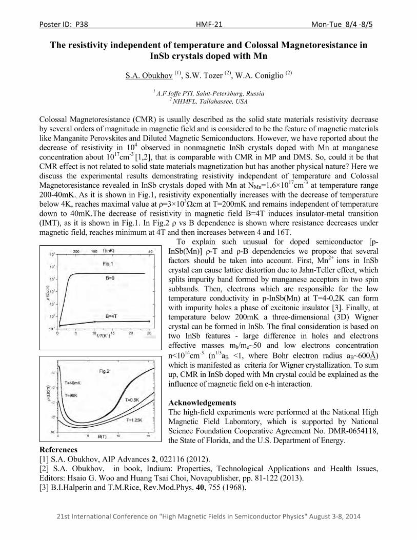
Poster ID: P38 HMF-‐21 Mon-‐Tue 8/4 -‐8/5
21st International Conference on "High Magnetic Fields in Semiconductor Physics" August 3-‐8, 2014
The resistivity independent of temperature and Colossal Magnetoresistance in InSb crystals doped with Mn
S.A. Obukhov (1), S.W. Tozer (2), W.A. Coniglio (2)
1 A.F.Ioffe PTI, Saint-Petersburg, Russia
2 NHMFL, Tallahassee, USA Colossal Magnetoresistance (CMR) is usually described as the solid state materials resistivity decrease by several orders of magnitude in magnetic field and is considered to be the feature of magnetic materials like Manganite Perovskites and Diluted Magnetic Semiconductors. However, we have reported about the decrease of resistivity in 104 observed in nonmagnetic InSb crystals doped with Mn at manganese concentration about 1017cm-3
[1,2], that is comparable with CMR in MP and DMS. So, could it be that CMR effect is not related to solid state materials magnetization but has another physical nature? Here we discuss the experimental results demonstrating resistivity independent of temperature and Colossal Magnetoresistance revealed in InSb crystals doped with Mn at NMn=1,6×1017cm-3 at temperature range 200-40mK.. As it is shown in Fig.1, resistivity exponentially increases with the decrease of temperature below 4K, reaches maximal value at ρ=3×10³Ωcm at T=200mK and remains independent of temperature down to 40mK.The decrease of resistivity in magnetic field B=4T induces insulator-metal transition (IMT), as it is shown in Fig.1. In Fig.2 ρ vs B dependence is shown where resistance decreases under magnetic field, reaches minimum at 4T and then increases between 4 and 16T.
To explain such unusual for doped semiconductor [p-InSb(Mn)] ρ-T and ρ-B dependencies we propose that several factors should be taken into account. First, Mn2+ ions in InSb crystal can cause lattice distortion due to Jahn-Teller effect, which splits impurity band formed by manganese acceptors in two spin subbands. Then, electrons which are responsible for the low temperature conductivity in p-InSb(Mn) at T=4-0,2K can form with impurity holes a phase of excitonic insulator [3]. Finally, at temperature below 200mK a three-dimensional (3D) Wigner crystal can be formed in InSb. The final consideration is based on two InSb features - large difference in holes and electrons effective masses mh/me~50 and low electrons concentration n<1014cm-3 (n1/3aB <1, where Bohr electron radius aB~600Å) which is manifested as criteria for Wigner crystallization. To sum up, CMR in InSb doped with Mn crystal could be explained as the influence of magnetic field on e-h interaction. Acknowledgements The high-field experiments were performed at the National High Magnetic Field Laboratory, which is supported by National Science Foundation Cooperative Agreement No. DMR-0654118, the State of Florida, and the U.S. Department of Energy.
References [1] S.A. Obukhov, AIP Advances 2, 022116 (2012). [2] S.A. Obukhov, in book, Indium: Properties, Technological Applications and Health Issues, Editors: Hsaio G. Woo and Huang Tsai Choi, Novapublisher, pp. 81-122 (2013). [3] B.I.Halperin and T.M.Rice, Rev.Mod.Phys. 40, 755 (1968).
Poster ID: P39 HMF-‐21 Mon-‐Tue 8/4 -‐8/5
21st International Conference on "High Magnetic Fields in Semiconductor Physics" August 3-‐8, 2014
Rheological Effects of Magnetic Treatment of Wax Oils
A.D. Sheikh-Alia,b, A.B. Auezova, M.N. Esimkulovaa,b, T. Omarovaa, D. Turkmenovaa and M. Ibraimova
aInstitute of Rheotechnologies LLC, 161-1 Kozhamkulova Street, 050026, Almaty, Kazakhstan
bKazakh-British Technical University, 59 Tole-bi Street, 050000, Almaty, Kazakhstan In this study, series of experiments have been carried out to establish the effect of DC magnetic field on rheological parameters of oil such as viscosity, pour point and wax deposition rate. The obtained results demonstrate that depending on the oil composition, the magnetic treatment can lead to different results. For oils with respectively low paraffin content (3-5%) and high resin content (17-18%), a significant reduction in viscosity (17-23%) have been observed after magnetic treatment. Whereas magnetic treatment of the high paraffin (~20%) and high resin (16-17%) oils results in a drastic increase in their viscosity (30-50%). The magnetic field can also inhibit wax deposition. In the case of low paraffin and high resin oils the inhibition degree can reach 95%. The mechanisms of the effects above remain unclear. To clarify perspectives of practical application of those effects, their relaxation time has been assessed.
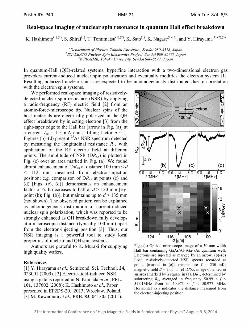
Poster ID: P40 HMF-‐21 Mon-‐Tue 8/4 -‐8/5
21st International Conference on "High Magnetic Fields in Semiconductor Physics" August 3-‐8, 2014
Real-space imaging of nuclear spin resonance in quantum Hall effect breakdown
K. Hashimoto(1),(2), S. Shirai(1), T. Tomimatsu(1),(2), K. Sato(1), K. Nagase(1),(2), and Y. Hirayama(1),(2),(3)
1Department of Physics, Tohoku University, Sendai 980-8578, Japan 2JST-ERATO Nuclear Spin Electronics Project, Sendai 980-8578i, Japan
3WPI-AIMR, Tohoku University, Sendai 980-8577, Japan
In quantum-Hall (QH)-related systems, hyperfine interaction with a two-dimensional electron gas provokes current-induced nuclear spin polarization and eventually modifies the electron system [1]. Resulting polarized nuclear spins are expected to be inhomogenously distributed due to correlation with the electron spin systems. We performed real-space imaging of resistively-detected nuclear spin resonance (NSR) by applying a radio-frequency (RF) electric field [2] from an atomic-force-microscope tip. Nuclear spins of the host materials are electrically polarized in the QH effect breakdown by injecting electron [3] from the right-taper edge to the Hall bar [arrow in Fig. (a)] at a current Isd = 1.5 mA and a filling factor n ~ 1. Figures (b)–(d) present 75As NSR spectrum detected by measuring the longitudinal resistance Rxx with application of the RF electric field at different points. The amplitude of NSR (DRxx) is plotted in Fig. (e) over an area marked in Fig. (a). We found abrupt enhancement of DRxx at distance 100 mm < d < 112 mm measured from electron-injection position; e.g. comparison of DRxx at points (c) and (d) [Figs. (c), (d)] demonstrates an enhancement factor of 6. It decreases to half at d > 120 mm [e.g. point (b); Fig. (b)], but maintains up to d > 135 mm (not shown). The observed pattern can be explained as inhomogeneous distribution of current-induced nuclear spin polarization, which was reported to be strongly enhanced as QH breakdown fully develops at a macroscopic distance (typically 100 mm) apart from the electron-injecting position [3]. Thus, our NSR imaging is a powerful tool to study local properties of nuclear and QH spin systems. Authors are grateful to K. Muraki for supplying high quality wafers.
References [1] Y. Hirayama et al., Semicond. Sci. Technol. 24, 023001 (2009). [2] Electric-field-induced NSR using a gate is reported in N. Kumada et al., PRL. 101, 137602 (2008); K. Hashimoto et al., Paper presented in EP2DS-20, 2013, Wroclaw, Poland. [3] M. Kawamura et al., PRB. 83, 041305 (2011).
Fig.: (a) Optical microscope image of a 30-mm-width Hall bar containing GaAs/Al0.3Ga0.7As quantum well. Electrons are injected as marked by an arrow. (b)–(d) Local resistively-detected NSR spectra recorded at points [marked in (e)]; temperature T ~ 230 mK; magnetic field B = 7.05 T. (e) DRxx image obtained in an area [marked by a square in (a). DRxx determined by subtracting Rxx averaged in frequency 50.99 < f < 51.01MHz from in 50.973 < f < 50.977 MHz. Horizontal axis indicates the distance measured from the electron-injecting position.
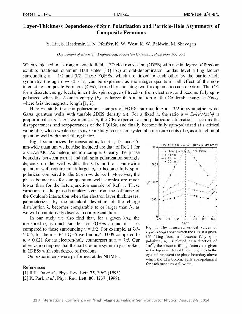
Poster ID: P41 HMF-‐21 Mon-‐Tue 8/4 -‐8/5
21st International Conference on "High Magnetic Fields in Semiconductor Physics" August 3-‐8, 2014
Layer-Thickness Dependence of Spin Polarization and Particle-Hole Asymmetry of Composite Fermions
Y. Liu, S. Hasdemir, L. N. Pfeiffer, K. W. West, K. W. Baldwin, M. Shayegan
Department of Electrical Engineering, Princeton University, Princeton, NJ, USA
When subjected to a strong magnetic field, a 2D electron system (2DES) with a spin degree of freedom exhibits fractional quantum Hall states (FQHSs) at odd-denominator Landau level filling factors surrounding n = 1/2 and 3/2. These FQHSs, which are linked to each other by the particle-hole symmetry through n ↔ (2 - n), can be explained as the integer quantum Hall effect of the non-interacting composite Fermions (CFs), formed by attaching two flux quanta to each electron. The CFs form discrete energy levels, inherit the spin degree of freedom from electrons, and become fully spin-polarized when the Zeeman energy (EZ) is larger than a fraction of the Coulomb energy, e2/4πεlB, where lB is the magnetic length [1, 2]. Here we study the spin-polarization energies of FQHSs surrounding n = 3/2 in symmetric, wide, GaAs quantum wells with tunable 2DES density (n). For a fixed n, the ratio α = EZ/(e2/4πεlB) is proportional to n1/2. As we increase n, the CFs experience spin-polarization transitions, seen as the disappearances and reappearances of the FQHSs, and finally become fully spin-polarized at a critical value of α, which we denote as αc. Our study focuses on systematic measurements of αc as a function of quantum well width and filling factor. Fig. 1 summarizes the measured αc for 31-, 42- and 65-nm-wide quantum wells. Also included are data of Ref. 1 for a GaAs/AlGaAs heterojunction sample. Clearly the phase boundary between partial and full spin polarization strongly depends on the well width: the CFs in the 31-nm-wide quantum well require much larger αc to become fully spin-polarized compared to the 65-nm-wide well. Moreover, the phase boundaries for our quantum well samples are much lower than for the heterojunction sample of Ref. 1. These variations of the phase boundary stem from the softening of the Coulomb interaction when the electron layer thicknesses, parameterized by the standard deviation of the charge distribution λ, becomes comparable to or larger than lB, as we will quantitatively discuss in our presentation. In our study we also find that, for a given λ/lB, the measured αc is much smaller for FQHSs around n = 1/2 compared to those surrounding ν = 3/2. For example, at λ/lB ≈ 0.6, for the n = 3/5 FQHS we find αc ≈ 0.009 compared to αc ≈ 0.021 for its electron-hole counterpart at n = 7/5. Our observation implies that the particle-hole symmetry is broken in 2DESs with spin degree of freedom. Our experiments were performed at the NHMFL.
References [1] R.R. Du et al., Phys. Rev. Lett. 75, 3962 (1995). [2] K. Park et al., Phys. Rev. Lett. 80, 4237 (1998).
Fig. 1: The measured critical values of EZ/(e2/4πεlB) above which the CFs at a given CF filling factor nCF become fully spin-polarized, αc, is plotted as a function of 1/nCF; the electron filling factors are given in the top axis. Dotted lines are guides to the eye and represent the phase boundary above which the CFs become fully spin-polarized for each quantum well width.

Poster ID: P42 HMF-‐21 Mon-‐Tue 8/4 -‐8/5
21st International Conference on "High Magnetic Fields in Semiconductor Physics" August 3-‐8, 2014
Even-denominator Fractional Quantum Hall Effect at a Landau Level Crossing
Yang Liu, H. Deng, S. Hasdemir, L. N. Pfeiffer, K. W. West, K. W. Baldwin, M. Shayegan
Department of Electrical Engineering, Princeton University, Princeton, NJ, USA
A strong perpendicular magnetic field B applied to a two-dimensional (2D) electron system quantizes the electron energies into discrete Landau levels (LLs). At very low temperatures, and if disorder is low, electron-electron interaction leads to new phenomena. An example is the fractional quantum Hall effect (FQHE), the condensation of 2D electrons into many-body incompressible states which are stable predominantly at odd-denominator fractional LL filling factors n. Here we describe unexpected phenomena in 2D hole systems (2DHSs) confined to GaAs quantum wells (QWs). In our study, we observe an unusual crossing of the two lowest-energy LLs. This crossing leads to a weakening or disappearance of the commonly seen odd-denominator FQHE states in the filling range 1/3 ≤ ν ≤ 2/3. But, surprisingly, a new FQHE state at the even-denominator filling ν = 1/2 comes to life at the crossing. Our results attest to the rich many-body physics of the 2DHSs. Figure 1 captures the highlights of our work. We show the longitudinal (Rxx) and Hall (Rxy) resistance traces for a 2DHS confined to a 30-nm-wide QW for several densities, ranging from p = 1.20 to 1.72 (in units of 1011 cm-2). At the lowest p (top trace), Rxx minima are observed at numerous odd-denominator fillings such as n = 2/3, 2/5, 3/5, 3/7, 4/7, etc. As p increases, starting at ≈ 1.32, an Rxx minimum develops at n = 1/2, and quickly deepens and turns into a zero-resistance plateau centered at n = 1/2 for p = 1.47. Concomitantly, the Rxy trace exhibits a Hall plateau quantized at 2h/e2, signaling the formation of a strong FQHE state at n = 1/2. At a slightly higher density, p = 1.59, the n = 1/2 Rxx minimum becomes weak. The strong n = 1/2 minimum returns again at higher p and the n = 1/2 FQHE persists up to the highest densities we can achieve in this sample. The behavior of Rxx near n = 1/2, and in particular the strengths of the nearby FQHE states, provide clear demonstration of an unusual crossing of the two lowest-energy hole energy levels in a large perpendicular magnetic field. Surprisingly, the n = 1/2 FQHE is very strong at this crossing and becomes weaker on either side of the crossing, while all the odd-denominator FQHE states, on the other hand, are strong except at the crossing. We tentatively interpret this FQHE as a two-component Y331 state. A detailed understanding of its origin and properties await future research.
References [1] Yang Liu et al., Phys. Rev. Lett. 112, 046804 (2014). [2] Yang Liu et al., Phys. Rev. B 89, 165313 (2014).
Fig. 1: Longitudinal and Hall resistances measured at T ≈ 30 mK in a 2DHS confined to a 30-nm-wide GaAs QW, at different densities p.

Poster ID: P43 HMF-‐21 Mon-‐Tue 8/4 -‐8/5
21st International Conference on "High Magnetic Fields in Semiconductor Physics" August 3-‐8, 2014
Pump-probe nuclear electric resonance measurement using QHE breakdown
T. Tomimatsu (1),(2), S. Shirai (1), K. Hashimoto (1),(2), K. Sato(1), and Y. Hirayama(1),(2),(3)
1Department of Physics, Tohoku University, Sendai 980-8578, Japan 2JST-ERATO Nuclear Spin Electronics Project, Sendai 980-8578, Japan
3WPI-AIMR, Tohoku University, Sendai 980-8577, Japan
In quantum Hall system (QHS), by applying AC electric field to back gate, nuclear electric resonance (NER) was confirmed to be driven at filling factor n = 2/3 spin phase transition [1] and n = 1 QHE breakdown [2]. Although the models of nuclear spin relaxation under oscillated electric field were proposed, NER mechanisms in QHS still remain unclear. In this study, we further investigate NER for wider range of filling factors and temperatures by pump-probe method using QHE breakdown. First, the nuclear spin was polarized at breakdown regime by applying current I = 2 mA at n = 1. Then I was set to zero and NER was performed at different n by controlling DC and AC RF voltages of the back gate. Finally, I and n were set back to I = 2 mA and n = 1 to detect the longitudinal resistance change DR of before and after NER for assessing the nuclear spin relaxation. Figure 1 is an example of NER spectra taken at temperature T = 1.2 K. At n = 0.6‐2.1, DR shows resonance features of 75As including the effect of Knight shift, while it is not observed at depletion (n = 0). In particular, DR peak intensity is enhanced at integer n (n = 1.0 and 2.0). This indicates the possibility that NER is correlated with electron states in integer quantum Hall regime at higher temperature. Our findings give important insight into imaging or local probing of nuclear spin resonance using modulated electric field [3]. Authors are grateful to K. Muraki for supplying the wafers, to K. Yamaguchi for sample fabrication.
References [1] N. Kumada et al., Phys. Rev. Lett. 101, 137602 (2008). [2] K. Hashimoto et al., Abst. of 40th Int. Sym. on Compound Semiconductors (2013). [3] K. Hashimoto et al., Abst. of 20th Int. Conf. on Electronic Properties of Two-Dimensional Systems (2013).
Fig. 1: n dependence of NER spectra taken for magnetic field B = 7.05 T at T = 1.2 K. Power of RF applying to the back gate is P = -5 dBm.
Poster ID: P44 HMF-‐21 Mon-‐Tue 8/4 -‐8/5
21st International Conference on "High Magnetic Fields in Semiconductor Physics" August 3-‐8, 2014
An intuitive approach to correlations in the ν= 5/2 quantum Hall state
J. J. Quinn(1), R. E. Wooten (1), J. H. Macek (1)
1University of Tennessee, Knoxville, USA
Moore and Read proposed a trial wave function ΨMR for the ν = 5/2 spin polarized quantum Hall (QH) state. ΨMR is a product of the square of a Fermionic factor F = ∏i<j zij and a “correlator” used in conformal field theory, Pf{zij
-1}. The “correlator” is called a Pfaffian, and it is equivalent to the antisymmetrized product Â{(z1,2 z3,4 … zN-1,N)-1} where zij = zi – zj. It is apparent that ΨMR contains no factor of zi (for any value of i) to a power higher than 2N-3, since F2 contains zi
2(N-1) while Pf{zij-1}
contains a sum of terms each of which contains a factor zi-1. A simpler, but seemingly different wave
function can be constructed by multiplying the antisymmetric Fermionic factor F by a symmetric “quadratic” correlation function GQ{zij}. We partition the N particles into two subsets each containing N/2. One partition, for example, could be gA = {1, 3, …, N-1}, gB = {2, 4, …, N}. Then, we propose GQ{zij} be equal to ŜN{∏i<j in gA zij
2 ∏k<l in gB zkl2}, where ŜN symmetrizes the product in curly brackets
over all N particles. ΨQ = F*GQ also has no factor of any zi larger than 2N-3, since F contains zi(N-1)
and GQ contains zi2(N/2-1). It is interesting to compare GMR and GQ. GMR for a system of four electrons
is (z12 z13 z24 z34 – z12 z14 z23 z34 + z13 z14 z23 z24), while GQ = (z122 z34
2 + z132 z24
2 + z142 z23
2). It is useful to draw diagrams for each term in G in which a factor zij is represented as a single line and zij
2 by a double line connecting particles i and j. The number of lines originating on any particle i can be determined from the value of 2l which must equal ν-1N-cv, where cv is the “finite size” shift and can be obtained by a simple heuristic argument. Diagrams for contributions to the wave function Ψ must include ½N(N-1) additional lines associated with F. The diagrams for ΨMR and ΨQ are different. However, both can be written as a Fermion factor multiplied by a homogeneous polynomial. Surprisingly, the homogeneous polynomials for ΨMR and ΨQ in the four-particle case are the same when the wave functions are normalized. We conjecture that this will be true for arbitrary N, and are checking for other special cases, and seeking a rigorous proof. We believe a similar intuitive approach can be used for Jain states (e.g. ν = 2/5) and for Laughlin states containing a few quasiparticles. The partitioning is different for different values of ν.

Poster ID: P45 HMF-‐21 Mon-‐Tue 8/4 -‐8/5
21st International Conference on "High Magnetic Fields in Semiconductor Physics" August 3-‐8, 2014
Permutation group symmetry, partitions, and correlations in quantum Hall systems
J. J. Quinn(1)
1University of Tennessee, Knoxville, USA
Incompressible quantum Hall states occur when the single particle angular momentum l and the number N of electrons in a partially filled Landau level satisfy the relation 2l = ν-1N-cv. Here, ν is the filling factor, and cv is the “finite size shift.” The value of cv can be obtained from a simple heuristic argument, and it gives useful information about correlations. A trial wave function Ψ can always be written as a product of an antisymmetric Fermion factor F{zij} caused by the Pauli principle, and a symmetric correlation function G{zij} caused by interactions. Both factors involve products, or sums of products, of correlation factors zij. The maximum power of any zi in Ψ cannot exceed 2l in order to fit Ψ into the finite Hilbert space defined by (N, 2l).
Diagrams can be constructed in which each factor of zij is represented by a single line connecting particles i and j. Due to F{zij} = ∏i<j zij, (N-1) powers of zi appear, leaving 2l-(N-1) powers of zi associated with G{zij}. A diagram contributing to G{zij} can contain no more than 2l+1-N lines (factors zij) emanating from any particle i. This fact, together with translational invariance (required for an L=0 state) and permutation symmetry greatly restrict the possible choices for G{zij}. We illustrate this novel method of constructing trial wave functions for correlations appropriate to the ν = 5/2 (Moore-Read states), to Laughlin-Jain states at ν = n(1+2n)-1, and for states containing a few quasiparticles in a Laughlin incompressible quantum liquid state.
Out[416]=
Figure 1. Diagram of the wavefunction for N = 8 particles and 2l = 13 for the nu = 5/2 state. Grey lines indicate terms with zij
3 for Laughlin correlations within the set of particles gB = {2, 4, 6, 8}; pale grey lines indicate terms with zij
3 for Laughlin correlations within the set of particles gA = {1,3,5,7} ; and finally, the remaining black lines indicate terms with zij for the Fermi factor, indicating no correlations between groups gA and gB.
Poster ID: P46 HMF-‐21 Mon-‐Tue 8/4 -‐8/5
21st International Conference on "High Magnetic Fields in Semiconductor Physics" August 3-‐8, 2014
On the absence of higher generations of composite Fermions in quantum Hall systems
J. J. Quinn (1)
1University of Tennessee, Knoxville, USA
The interaction energy, V(L2), of a pair of electrons in a quantum Hall (QH) system depends on the pair angular momentum L2. L2 = 2l-R2, where l is the single particle angular momentum and R2 is an odd integer. If V(L2) is proportional to the eigenvalue of the square of L2, every multiplet |L,α> with the same value of total angular momentum L has the same energy. Laughlin realized that an incompressible quantum liquid (IQL) state would occur when the electrons avoided pair states with the largest repulsion (largest values of L2). He proposed an antisymmetric trial wave function for filling factor ν equal to the reciprocal of an odd integer. Jain noticed that the most robust IQL states occurred at ν = n*(1+2n)-1, where n is an integer. He suggested that the introduction of a “Chern-Simons” gauge field attached to each electron led, in the mean field (MF) approximation, to a system of non-interacting composite Fermions (CFs) moving in an effective magnetic field B*=B-2nϕ. He suggested that the fractional QH effect was simply the integral QH effect of CFs. Chen and Quinn determined that the angular momenta lQP of CF quasiparticles. They demonstrated that Jain’s simple MFCF picture could correctly predict the total angular momentum L of each multiplet |L,α> in the lowest band of energy levels for any value of the magnetic field B. Despite its success, Jain’s simple CF picture was not universally accepted. It has been justified, using rigorous mathematical theorems, when the pseudopotential of the interacting Fermions satisfies the conditions necessary to support Laughlin correlations. These conditions are not satisfied for quasielectrons (QEs) of the Laughlin ν = 1/3 state, implying that a second generation of CFs cannot be the cause of an IQL daughter state of a spin polarized electron system at νQE=1/3.
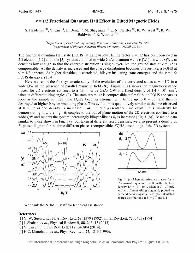
Poster ID: P47 HMF-‐21 Mon-‐Tue 8/4 -‐8/5
21st International Conference on "High Magnetic Fields in Semiconductor Physics" August 3-‐8, 2014
ν = 1/2 Fractional Quantum Hall Effect in Tilted Magnetic Fields
S. Hasdemir (1), Y. Liu (1), H. Deng (1), M. Shayegan (1), L. N. Pfeiffer (1), K. W. West (1), K. W. Baldwin (1), R. Winkler (2)
1Department of Electrical Engineering, Princeton University, Princeton NJ, USA
2Department of Physics, Northern Illinois University, DeKalb IL, USA
The fractional quantum Hall state (FQHS) at Landau level filling factor ν = 1/2 has been observed in 2D electron [1,2] and hole [3] systems confined to wide GaAs quantum wells (QWs). In wide QWs, at densities low enough so that the charge distribution is single-layer-like, the ground state at ν = 1/2 is compressible. As the density is increased and the charge distribution becomes bilayer-like, a FQHS at ν = 1/2 appears. At higher densities, a correlated, bilayer insulating state emerges and the ν = 1/2 FQHS disappears [3,4]. Here we report the first systematic study of the evolution of the correlated states at ν = 1/2 in a wide QW in the presence of parallel magnetic field (B||). Figure 1 (a) shows the magnetoresistance traces, for 2D electrons confined to a 65-nm-wide GaAs QW at a fixed density of 1.4 × 1011 cm-2, taken at different tilting angles (θ). The state at ν = 1/2 is compressible at θ = 0° but a FQHS appears as soon as the sample is tilted. The FQHS becomes stronger with tilting up to θ = 35° and then is destroyed at higher θ by an insulating phase. This evolution is qualitatively similar to the one observed at θ = 0° as the density is increased [1-4]. In our presentation, we explain this similarity by demonstrating how the high B|| couples to the out-of-plane motion of the 2D electrons confined to a wide QW and renders the system increasingly bilayer-like as B|| is increased [Fig. 1 (b)]. Based on data similar to those shown in Fig. 1 (a) but taken at different fixed densities, we also present a density vs B|| phase-diagram for the three different phases (compressible, FQHS, insulating) of the 2D system.
We thank the NHMFL staff for technical assistance. References [1] Y. W. Suen et al., Phys. Rev. Lett. 68, 1379 (1992); Phys. Rev.Lett. 72, 3405 (1994). [2] J. Shabani et al., Physical Review B, 88, 245413 (2013). [3] Y. Liu et al., Phys. Rev. Lett. 112, 046804 (2014). [4] H.C. Manoharan et al., Phys. Rev. Lett. 77, 1813 (1996).
Fig. 1: (a) Magnetoresistance traces for a 65-nm-wide quantum well with electron density 1.4 × 1011 cm-2, taken at T ~ 30 mK and at different tilting angles θ, plotted vs perpendicular magnetic field. (b) Calculated charge distributions at B|| = 0 T and 8 T.
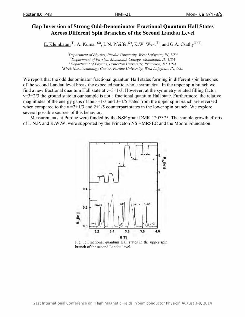
Poster ID: P48 HMF-‐21 Mon-‐Tue 8/4 -‐8/5
21st International Conference on "High Magnetic Fields in Semiconductor Physics" August 3-‐8, 2014
Gap Inversion of Strong Odd-Denominator Fractional Quantum Hall States Across Different Spin Branches of the Second Landau Level
E. Kleinbaum(1), A. Kumar (2), L.N. Pfeiffer(3), K.W. West(3), and G.A. Csathy(1)(4)
1Department of Physics, Purdue University, West Lafayette, IN, USA
2Department of Physics, Monmouth College, Monmouth, IL, USA 3Department of Physics, Princeton University, Princeton, NJ, USA
4Birck Nanotechnology Center, Purdue University, West Lafayette, IN, USA We report that the odd denominator fractional quantum Hall states forming in different spin branches of the second Landau level break the expected particle-hole symmetry. In the upper spin branch we find a new fractional quantum Hall state at ν=3+1/3. However, at the symmetry-related filling factor ν=3+2/3 the ground state in our sample is not a fractional quantum Hall state. Furthermore, the relative magnitudes of the energy gaps of the 3+1/3 and 3+1/5 states from the upper spin branch are reversed when compared to the ν =2+1/3 and 2+1/5 counterpart states in the lower spin branch. We explore several possible sources of this behavior. Measurements at Purdue were funded by the NSF grant DMR-1207375. The sample growth efforts of L.N.P. and K.W.W. were supported by the Princeton NSF-MRSEC and the Moore Foundation.
Fig. 1: Fractional quantum Hall states in the upper spin branch of the second Landau level.

Poster ID: P49 HMF-‐21 Mon-‐Tue 8/4 -‐8/5
21st International Conference on "High Magnetic Fields in Semiconductor Physics" August 3-‐8, 2014
Contribution of weak localization and electron-electron interaction, in corrective term “mT1/2” of the metallic conductivity in n-type SiAs with magnetic field
Jamal Hemine 1, Abdelhamid El kaaouachi 2
1 Laboratoire de Physique de la Matière Condensée, Faculté des Sciences et Techniques de Mohammadia, Département de
Physique, Mohammadia, Morocco. 2 Physics Department, University Ibn Zohr, Faculty of Sciences, B.P 8106, Hay Dakhla, 80000 Agadir, Morocco.
We present measurements of the electrical conductivity of barely metallic n-type SiAs that are driven to the metal-insulator transition (MIT) by impurity concentration. The experiments were carried out at low temperature in the range (3.48 - 0.00044 K) and with impurity concentrations up . On the metallic side of the MIT, the electrical conductivity is found to behave like down to 0.44 mK. Physical explanation to the temperature dependence of the conductivity is given in metallic side of the MIT using a competition between two effects involved in the mechanisms of conduction, like electron-electron interaction effect, and weak localization effect. References [1] G. Biskupski et al., J. Phys Condens Matter. 3 (1991) 8417. [2] A. El kaaouachi et al., Phys. Stat. Sol b. 241 No 1 (2004) 155-162. [3] A. El kaaouachi et al., Physica B Condens Matter. 226 N°3 (1998) 226- 228. [4] A. El kaaouachi et al., Physica B Condens Matter . 304 (2001) 377-381 [5] A. El kaaouachi et al., Semiconductors Sciences and Technology.18 (2003) 69-74. [6] G. A. Thomas et al., Phys. Rev B 26 (1982) 2113 [7] G. A. Thomas et al., M. Paalmen, and T. F. Rosenbaum, Phys. Rev B 27 (1983) 3897 [8] W. N. Shafarman et al., Phys. Rev B 40 (1988) 1216. [9] BL. Altshuler et al., Sov. Phys –JETP. 54(1981) 411. [10] FJ. Wegner, Z. phys. B 35 (1979) 2007. [11] A. Kawabata, solid state commun. 34 (1980) 431. [12] L. Kleiman, Phys. Rev. 160 (1967) 585. [13] DG. Langreth, Phys Rev. 181 (1967) 753.
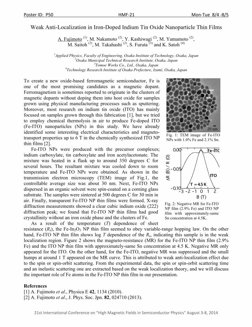
Poster ID: P50 HMF-‐21 Mon-‐Tue 8/4 -‐8/5
21st International Conference on "High Magnetic Fields in Semiconductor Physics" August 3-‐8, 2014
Fig. 1: TEM image of Fe-ITO NPs with 1.0% Fe and 2.1% Sn.
20 nm
Weak Anti-Localization in Iron-Doped Indium Tin Oxide Nanoparticle Thin Films
A. Fujimoto (1), M. Nakamoto (2), Y. Kashiwagi (2), M. Yamamoto (2), M. Saitoh (2), M. Takahashi (2), S. Furuta (3) and K. Satoh (4)
1Applied Physics, Faculty of Engineering, Osaka Institute of Technology, Osaka, Japan
2Osaka Municipal Technical Research Institute, Osaka, Japan 3Tomoe Works Co., Ltd., Osaka, Japan
4Technology Research Institute of Osaka Prefecture, Izumi, Osaka, Japan
To create a new oxide-based ferromagnetic semiconductor, Fe is one of the most promising candidates as a magnetic dopant. Ferromagnetism is sometimes reported to originate in the clusters of magnetic dopants without doping them into host oxide for samples grown using physical manufacturing processes such as sputtering. Moreover, most research on indium tin oxide (ITO) has mainly focused on samples grown through this fabrication [1], but we tried to employ chemical thermolysis in air to produce Fe-doped ITO (Fe-ITO) nanoparticles (NPs) in this study. We have already identified some interesting electrical characteristics and magneto-transport properties up to 6 T in the chemically synthesized ITO NP thin films [2].
Fe-ITO NPs were produced with the precursor complexes; indium carboxylate, tin carboxylate and iron acetylacetonate. The mixture was heated in a flask up to around 350 degrees C for several hours. The resultant mixture was cooled down to room temperature and Fe-ITO NPs were obtained. As shown in the transmission electron microscopy (TEM) image of Fig.1, the controllable average size was about 30 nm. Next, Fe-ITO NPs dispersed in an organic solvent were spin-coated on a corning glass substrate. The samples were sintered at 500 degrees C for 30 min in air. Finally, transparent Fe-ITO NP thin films were formed. X-ray diffraction measurements showed a clear cubic indium oxide (222) diffraction peak; we found that Fe-ITO NP thin films had good crystallinity without an iron oxide phase and the clusters of Fe.
As a result of the temperature (T) dependence of sheet resistance (Rs), the Fe-In2O3 NP thin film seemed to obey variable-range hopping law. On the other hand, Fe-ITO NP thin film shows log T dependence of the Rs, indicating this sample is in the weak localization region. Figure 2 shows the magneto-resistance (MR) for the Fe-ITO NP thin film (2.9% Fe) and the ITO NP thin film with approximately-same Sn concentration at 4.5 K. Negative MR only appeared for the ITO. On the other hand, for the Fe-ITO, negative MR was suppressed and the small humps at around 1 T appeared on the MR curve. This is attributed to weak anti-localization effect due to the spin or spin-orbit scattering. From the experimental data, the spin or spin-orbit scattering time and an inelastic scattering one are extracted based on the weak localization theory, and we will discuss the important role of Fe atoms in the Fe-ITO NP thin film in our presentation.
References [1] A. Fujimoto et al., Physica E 42, 1134 (2010). [2] A. Fujimoto et al., J. Phys. Soc. Jpn. 82, 024710 (2013).
Fig. 2: Negative MR for Fe-ITO NP film (2.9% Fe) and ITO NP film with approximately-same Sn concentration at 4.5K.
Poster ID: P51 HMF-‐21 Mon-‐Tue 8/4 -‐8/5
21st International Conference on "High Magnetic Fields in Semiconductor Physics" August 3-‐8, 2014
Strong enhancement of the geometrical magnetoresistance in the GaN/AlGaN-based transistor structures with leaky gate electrodes
K. Nogajewski (1,2), K. Karpierz (2), F. Teppe (3), W. Knap (3,4), M. S. Shur (5), J. Łusakowski (2)
1Laboratoire National des Champs Magnétiques Intenses,CNRS-UJF-UPS-INSA, Grenoble, France
2Institute of Experimental Physics, Faculty of Physics, University of Warsaw, Warsaw, Poland 3Laboratoire Charles Coulomb (L2C),UMR CNRS 5221, GIS-TERALAB, Université Montpellier II, Montpellier, France
4Institute of High Pressure Physics, Polish Academy of Sciences, Warsaw, Poland 5Department of Electrical, Electronics, and System Engineering, Rensselear Polytechnic Institute, Troy, New York, USA
In recent years, a subject of linear, non-saturating magnetoresistance occurring up to very high magnetic fields (B) has acquired a lot of interest from both the experimental and theoretical points of view [1-3]. It was shown that macroscopically disordered materials, like non-magnetic silver chalcogenides, can posses such a property, which makes them ideally suited for the magnetic-field-sensing applications. In the present paper we demonstrate that a similar behavior can also be observed in field-effect transistors (FETs), provided that they are equipped with leaky gate electrodes - a defect that normally would bring them into discredit as valuable electronic devices. We have studied a set of large-area (about 1.6 mm × 1.6 mm) FETs processed on a high-quality GaN/AlGaN heterostructure grown on a sapphire substrate. It comprised of three gated samples and a reference structure of exactly the same dimensions but no gate electrode deposited on its top. Due to
high density (> 1013 cm-2) of a two-dimensional electron gas (2DEG) and resulting high occupancy of the Landau levels (about 20 at B = 10 T), the magnetotransport properties of our FETs were dominated by classical effects with only a small onset of quantum oscillations appearing above B = 7 T. We probed them by a series of two-terminal resistance measurements performed at 4.2 K and a constant gate polarization (Vg) as a function of B up to 10 T oriented either parallel or anti-parallel to the heterostructure growth's direction. An example of typical experimental data is shown with open symbols in Fig. 1. As can be seen, all traces exhibit a linear or nearly linear and non-saturating magnetoresistance in the high-B limit. Additionally, the slope of the linear part is much larger for the gated structure and varies with Vg in a non-monotonic way. We demonstrate that all these results can be
accurately reproduced by a semi-phenomenological model based on the conformal-mapping approach to description of the geometrical magnetoresistance, which takes into account an effective shrinking of the FET's channel caused by a significant current leaking through the gate electrode.
References [1] A. Husmann et al., Nature 417, 421 (2002). [2] M. M. Parish, and P. B. Littlewood, Phys. Rev. B. 72, 094417 (2005). [3] J. Hu, and T. F. Rosenbaum, Nature Mater. 7, 697 (2008).
Fig. 1: Magnetic-field dependence of the longitudinal resistivity of a 2DEG (open symbols), recorded for the sample without a gate electrode (T0) and a gated structure (T1) for various voltages applied to the gate. Solid curves represent the results of fitting the data with a semi-phenomenological model of the gate-leakage-current-enhanced geometrical magnetoresistance.
Poster ID: P52 HMF-‐21 Mon-‐Tue 8/4 -‐8/5
21st International Conference on "High Magnetic Fields in Semiconductor Physics" August 3-‐8, 2014
Poster ID: P53 HMF-‐21 Mon-‐Tue 8/4 -‐8/5
21st International Conference on "High Magnetic Fields in Semiconductor Physics" August 3-‐8, 2014
Strong enhancement of the spin susceptibility near the critical density in Si-MOSFETs with magnetic field
L. Limouny, A. El kaaouachi
aLaboratoire MSTI, Ecole Supérieure de Technologie d’Agadir, BP 33/S Agadir – Morocco
Corresponding author: [email protected] We analyze the electrical resistivity and conductivity of a dilute two dimensional electron gas (2DEG) in a Si MOSFET. When a magnetic field is applied parallel to the 2DEG plane, signature of complete spin polarization as evidenced by the saturation of the resistivity is observed. We measured the effective mass and the Landé g factor near the metal-insulator transition (MIT) and found the Landé g factor remains almost constant and close to its value in bulk silicon. In contrast, we have observed a sharp increase of the effective mass near the critical density of the MIT. Our new results suggest that the sharp increase in the previously observed spin susceptibility is mainly due to the enhanced effective mass. Therefore renormalization of the effective mass could play an important role in a dilute spin-polarized 2DEG. The data indicate that electron-electron interactions strongly modify the effective mass but only weakly affect the g-factor in a dilute 2DEG. Moreover, our results indicate that Bc, which corresponds to the magnetic field at that the magnetoresistivity reaches saturation, vanishes at a characteristic density higher than the critical density nc of the MIT. This is in contrast to the existing experimental results and requires further studies for understanding this discrepancy. References: [1] E. A. Abrahams, P. W. Anderson, D. C. Licciardello, and T. V. Ramakrishnan, Phys. Rev. Lett. 42, 673 (1979). [2] G. Dolan, D. D. Oshero, Phys. Rev. Lett. 43, 72 (1978). [3] M. J. Uren, R. A. Davies, M. Pepper, J. Phys. C 13, L986 (1980). [4] D. J. Bishop, D. C. Tsui, R. C. Dynes, Phys. Rev. Lett. 44, 1153 (1980). [5] S. V. Kravchenko, G. V. Kravchenko, J. E. Furneaux, V. M. Pudalov, and M. D’Iorio, Phys. Rev. B 50, 8039 (1994). [6] D. Popovic, A. B. Fowler, and S. Washburn, Phys. Rev. Lett. 79, 1543 (1997). [7] Y. Hanein, D. Shahar, J. Yoon, C. C. Li, D. C. Tsui, H. Shtrikman, Phys. Rev. B 58, R13338 (1998). [8] M. P. Lilly, J. L. Reno, J. A. Simmons, I. B. Spielman, J. P. Eisenstein, L. N. Pfeiffer, K. W. West, E. H. Hwang, S. Das Sarma, Phys. Rev. Lett. 90, 056806 (2003). [9] S. Das Sarma et al., Phys. Rev. Lett. 94, 136401 (2005). [10] A. P. Mills, Jr., A. P. Ramirez, L. N. Pfeiffer and K. W. West, Phys. Rev. Lett. 83, 2805 (1999). [11] M. J. Manfra, E. H. Hwang, S. Das Sarma, L.N. Pfeiffer, K.W. West, A.M. Sergent, Phys. Rev. Lett. 99, 236402 (2007). [12] K. Lai, W. Pan, DC Tsui, S. Lyon, M. Muhlberger, F. Schaffler, Phys. Rev. B. 75, 033314 (2007). [13] V. M. Pudalov, G. Brunthaler, A. Prinz, G. Bauer, JETP Lett. 65, 932 Cond-mat/9707054 [14] E. Tutuc, E. P. De Poortere, S. J. Papadakis, M. Shayegan, Phys. Rev. Lett. 86, 2858-2861(2001). [15] A.A Shashkin, Maryam Rahimi, S Anissimova, S.V Kravchenko, V.T Dolgopolov, T.M Klapwijk 272–276, Journal of Magnetism and Magnetic Materials e127–e132 (2004).
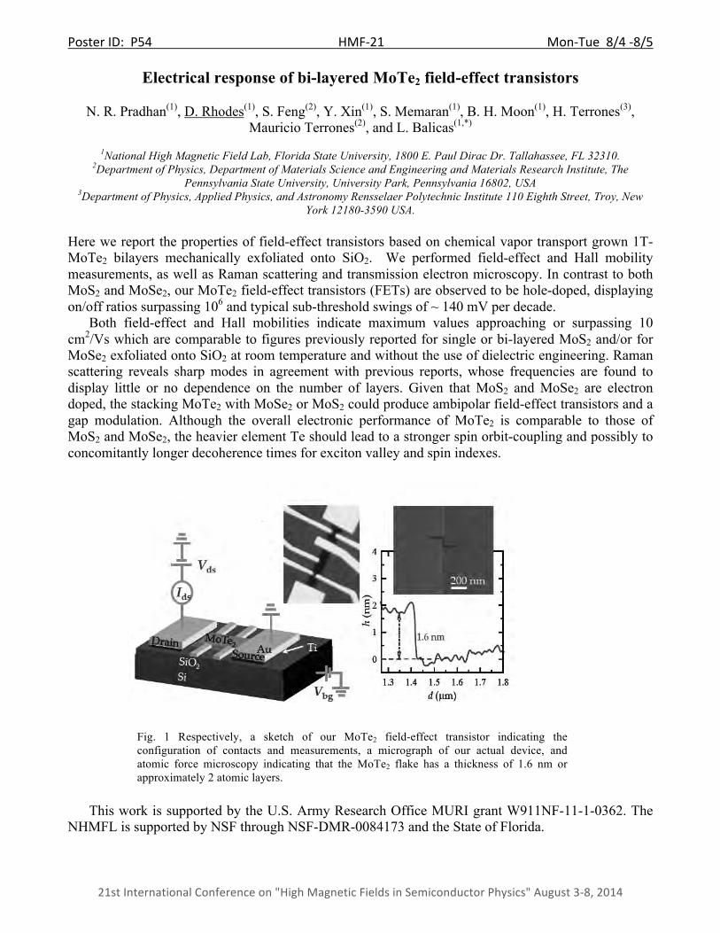
Poster ID: P54 HMF-‐21 Mon-‐Tue 8/4 -‐8/5
21st International Conference on "High Magnetic Fields in Semiconductor Physics" August 3-‐8, 2014
Electrical response of bi-layered MoTe2 field-effect transistors
N. R. Pradhan(1), D. Rhodes(1), S. Feng(2), Y. Xin(1), S. Memaran(1), B. H. Moon(1), H. Terrones(3), Mauricio Terrones(2), and L. Balicas(1,*)
1National High Magnetic Field Lab, Florida State University, 1800 E. Paul Dirac Dr. Tallahassee, FL 32310. 2Department of Physics, Department of Materials Science and Engineering and Materials Research Institute, The
Pennsylvania State University, University Park, Pennsylvania 16802, USA 3Department of Physics, Applied Physics, and Astronomy Rensselaer Polytechnic Institute 110 Eighth Street, Troy, New
York 12180-3590 USA. Here we report the properties of field-effect transistors based on chemical vapor transport grown 1T- MoTe2 bilayers mechanically exfoliated onto SiO2. We performed field-effect and Hall mobility measurements, as well as Raman scattering and transmission electron microscopy. In contrast to both MoS2 and MoSe2, our MoTe2 field-effect transistors (FETs) are observed to be hole-doped, displaying on/off ratios surpassing 106 and typical sub-threshold swings of ~ 140 mV per decade. Both field-effect and Hall mobilities indicate maximum values approaching or surpassing 10 cm2/Vs which are comparable to figures previously reported for single or bi-layered MoS2 and/or for MoSe2 exfoliated onto SiO2 at room temperature and without the use of dielectric engineering. Raman scattering reveals sharp modes in agreement with previous reports, whose frequencies are found to display little or no dependence on the number of layers. Given that MoS2 and MoSe2 are electron doped, the stacking MoTe2 with MoSe2 or MoS2 could produce ambipolar field-effect transistors and a gap modulation. Although the overall electronic performance of MoTe2 is comparable to those of MoS2 and MoSe2, the heavier element Te should lead to a stronger spin orbit-coupling and possibly to concomitantly longer decoherence times for exciton valley and spin indexes. This work is supported by the U.S. Army Research Office MURI grant W911NF-11-1-0362. The NHMFL is supported by NSF through NSF-DMR-0084173 and the State of Florida.
Fig. 1: Figures (grayscale preferable) and tables should be positioned appropriately on the page. Captions should be printed in single line spacing, Times Roman family 10pt. Fig. 1: Figures (grayscale preferable) and tables should be positioned appropriately on the page. Captions should be printed in single line spacing, Times Roman family 10pt.
Fig. 1: Figures (grayscale preferable) and tables should be positioned appropriately on the page. Captions should be printed in single line spacing, Times Roman family 10pt.
Fig. 1 Respectively, a sketch of our MoTe2 field-effect transistor indicating the configuration of contacts and measurements, a micrograph of our actual device, and atomic force microscopy indicating that the MoTe2 flake has a thickness of 1.6 nm or approximately 2 atomic layers.
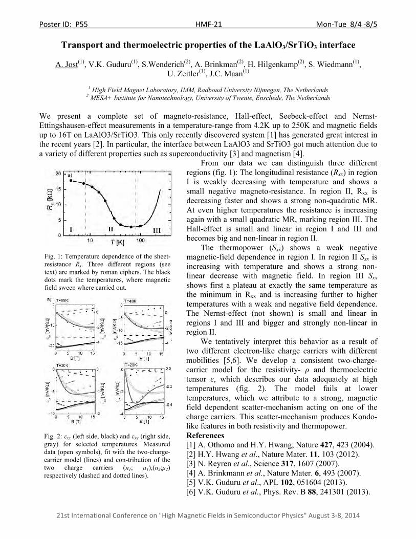
Poster ID: P55 HMF-‐21 Mon-‐Tue 8/4 -‐8/5
21st International Conference on "High Magnetic Fields in Semiconductor Physics" August 3-‐8, 2014
Transport and thermoelectric properties of the LaAlO3/SrTiO3 interface
A. Jost(1), V.K. Guduru(1), S.Wenderich(2), A. Brinkman(2), H. Hilgenkamp(2), S. Wiedmann(1), U. Zeitler(1), J.C. Maan(1)
1 High Field Magnet Laboratory, IMM, Radboud University Nijmegen, The Netherlands
2 MESA+ Institute for Nanotechnology, University of Twente, Enschede, The Netherlands
We present a complete set of magneto-resistance, Hall-effect, Seebeck-effect and Nernst-Ettingshausen-effect measurements in a temperature-range from 4.2K up to 250K and magnetic fields up to 16T on LaAlO3/SrTiO3. This only recently discovered system [1] has generated great interest in the recent years [2]. In particular, the interface between LaAlO3 and SrTiO3 got much attention due to a variety of different properties such as superconductivity [3] and magnetism [4].
From our data we can distinguish three different regions (fig. 1): The longitudinal resistance (Rxx) in region I is weakly decreasing with temperature and shows a small negative magneto-resistance. In region II, Rxx is decreasing faster and shows a strong non-quadratic MR. At even higher temperatures the resistance is increasing again with a small quadratic MR, marking region III. The Hall-effect is small and linear in region I and III and becomes big and non-linear in region II. The thermopower (Sxx) shows a weak negative magnetic-field dependence in region I. In region II Sxx is increasing with temperature and shows a strong non-linear decrease with magnetic field. In region III Sxx shows first a plateau at exactly the same temperature as the minimum in Rxx and is increasing further to higher temperatures with a weak and negative field dependence. The Nernst-effect (not shown) is small and linear in regions I and III and bigger and strongly non-linear in region II. We tentatively interpret this behavior as a result of two different electron-like charge carriers with different mobilities [5,6]. We develop a consistent two-charge-carrier model for the resistivity- ρ and thermoelectric tensor ε, which describes our data adequately at high temperatures (fig. 2). The model fails at lower temperatures, which we attribute to a strong, magnetic field dependent scatter-mechanism acting on one of the charge carriers. This scatter-mechanism produces Kondo-like features in both resistivity and thermopower. References [1] A. Othomo and H.Y. Hwang, Nature 427, 423 (2004). [2] H.Y. Hwang et al., Nature Mater. 11, 103 (2012). [3] N. Reyren et al., Science 317, 1607 (2007). [4] A. Brinkmann et al., Nature Mater. 6, 493 (2007). [5] V.K. Guduru et al., APL 102, 051604 (2013). [6] V.K. Guduru et al., Phys. Rev. B 88, 241301 (2013).
Fig. 1: Temperature dependence of the sheet- resistance Rs. Three different regions (see text) are marked by roman ciphers. The black dots mark the temperatures, where magnetic field sweep where carried out.
Fig. 2: εxx (left side, black) and εxy (right side, gray) for selected temperatures. Measured data (open symbols), fit with the two-charge-carrier model (lines) and con-tribution of the two charge carriers (n1; µ1),(n2;µ2) respectively (dashed and dotted lines).
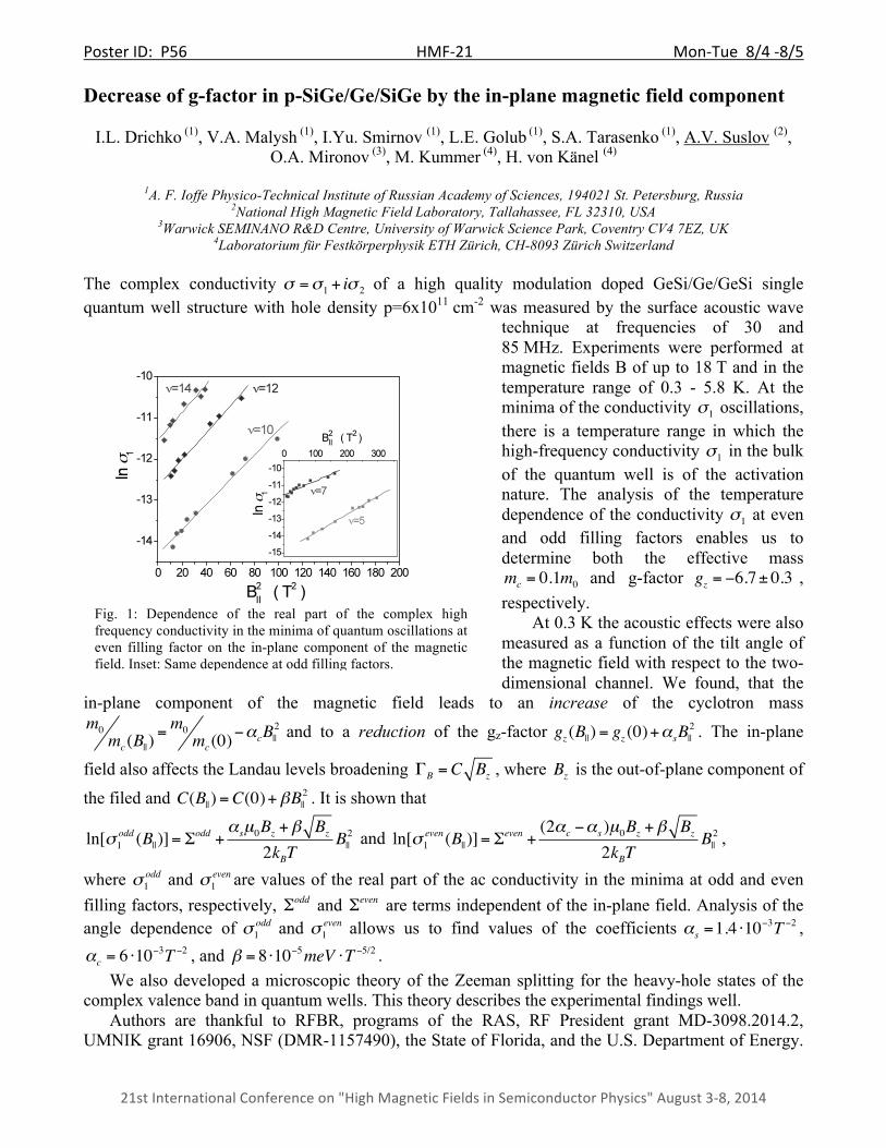
Poster ID: P56 HMF-‐21 Mon-‐Tue 8/4 -‐8/5
21st International Conference on "High Magnetic Fields in Semiconductor Physics" August 3-‐8, 2014
Decrease of g-factor in p-SiGe/Ge/SiGe by the in-plane magnetic field component
I.L. Drichko (1), V.A. Malysh (1), I.Yu. Smirnov (1), L.E. Golub (1), S.A. Tarasenko (1), A.V. Suslov (2), O.A. Mironov (3), M. Kummer (4), H. von Känel (4)
1A. F. Ioffe Physico-Technical Institute of Russian Academy of Sciences, 194021 St. Petersburg, Russia
2National High Magnetic Field Laboratory, Tallahassee, FL 32310, USA 3Warwick SEMINANO R&D Centre, University of Warwick Science Park, Coventry CV4 7EZ, UK
4Laboratorium für Festkörperphysik ETH Zürich, CH-8093 Zürich Switzerland
The complex conductivity σ =σ1 + iσ 2 of a high quality modulation doped GeSi/Ge/GeSi single quantum well structure with hole density p=6x1011 cm-2 was measured by the surface acoustic wave
technique at frequencies of 30 and 85 MHz. Experiments were performed at magnetic fields B of up to 18 T and in the temperature range of 0.3 - 5.8 K. At the minima of the conductivity σ1 oscillations, there is a temperature range in which the high-frequency conductivity σ1 in the bulk of the quantum well is of the activation nature. The analysis of the temperature dependence of the conductivity σ1 at even and odd filling factors enables us to determine both the effective mass mc = 0.1m0 and g-factor gz = −6.7± 0.3 , respectively. At 0.3 K the acoustic effects were also measured as a function of the tilt angle of the magnetic field with respect to the two-dimensional channel. We found, that the
in-plane component of the magnetic field leads to an increase of the cyclotron mass m0
mc (B|| )=m0
mc (0)−αcB||
2 and to a reduction of the gz-factor gz (B|| ) = gz (0)+αsB||2 . The in-plane
field also affects the Landau levels broadening ΓB =C Bz , where Bz is the out-of-plane component of
the filed and C(B|| ) =C(0)+βB||2 . It is shown that
ln[σ1odd (B|| )]= Σ
odd +αsµ0Bz +β Bz
2kBTB||2 and ln[σ1
even (B|| )]= Σeven +
(2αc −αs )µ0Bz +β Bz2kBT
B||2 ,
where σ1odd and σ1
even are values of the real part of the ac conductivity in the minima at odd and even filling factors, respectively, Σodd and Σeven are terms independent of the in-plane field. Analysis of the angle dependence of σ1
odd and σ1even allows us to find values of the coefficients αs =1.4 ⋅10
−3T −2 , αc = 6 ⋅10
−3T −2 , and β = 8 ⋅10−5meV ⋅T −5/2 . We also developed a microscopic theory of the Zeeman splitting for the heavy-hole states of the complex valence band in quantum wells. This theory describes the experimental findings well. Authors are thankful to RFBR, programs of the RAS, RF President grant MD-3098.2014.2, UMNIK grant 16906, NSF (DMR-1157490), the State of Florida, and the U.S. Department of Energy.
Fig. 1: Dependence of the real part of the complex high frequency conductivity in the minima of quantum oscillations at even filling factor on the in-plane component of the magnetic field. Inset: Same dependence at odd filling factors.
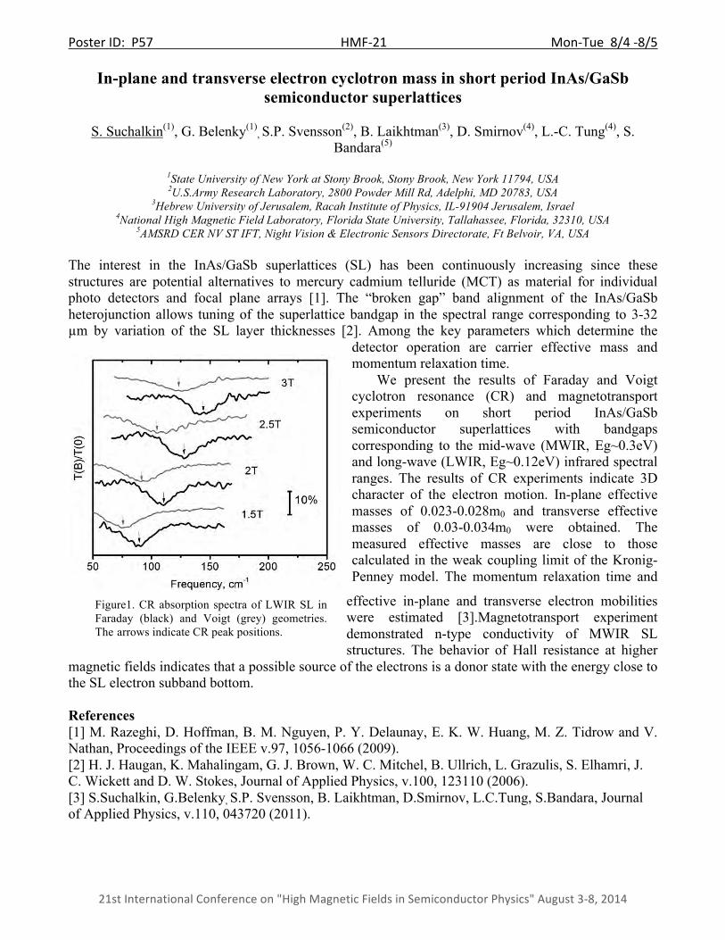
Poster ID: P57 HMF-‐21 Mon-‐Tue 8/4 -‐8/5
21st International Conference on "High Magnetic Fields in Semiconductor Physics" August 3-‐8, 2014
In-plane and transverse electron cyclotron mass in short period InAs/GaSb semiconductor superlattices
S. Suchalkin(1), G. Belenky(1)
, S.P. Svensson(2), B. Laikhtman(3), D. Smirnov(4), L.-C. Tung(4), S. Bandara(5)
1State University of New York at Stony Brook, Stony Brook, New York 11794, USA 2U.S.Army Research Laboratory, 2800 Powder Mill Rd, Adelphi, MD 20783, USA
3Hebrew University of Jerusalem, Racah Institute of Physics, IL-91904 Jerusalem, Israel
4National High Magnetic Field Laboratory, Florida State University, Tallahassee, Florida, 32310, USA 5AMSRD CER NV ST IFT, Night Vision & Electronic Sensors Directorate, Ft Belvoir, VA, USA
The interest in the InAs/GaSb superlattices (SL) has been continuously increasing since these structures are potential alternatives to mercury cadmium telluride (MCT) as material for individual photo detectors and focal plane arrays [1]. The “broken gap” band alignment of the InAs/GaSb heterojunction allows tuning of the superlattice bandgap in the spectral range corresponding to 3-32 µm by variation of the SL layer thicknesses [2]. Among the key parameters which determine the
detector operation are carrier effective mass and momentum relaxation time. We present the results of Faraday and Voigt cyclotron resonance (CR) and magnetotransport experiments on short period InAs/GaSb semiconductor superlattices with bandgaps corresponding to the mid-wave (MWIR, Eg~0.3eV) and long-wave (LWIR, Eg~0.12eV) infrared spectral ranges. The results of CR experiments indicate 3D character of the electron motion. In-plane effective masses of 0.023-0.028m0 and transverse effective masses of 0.03-0.034m0 were obtained. The measured effective masses are close to those calculated in the weak coupling limit of the Kronig-Penney model. The momentum relaxation time and
effective in-plane and transverse electron mobilities were estimated [3].Magnetotransport experiment demonstrated n-type conductivity of MWIR SL structures. The behavior of Hall resistance at higher
magnetic fields indicates that a possible source of the electrons is a donor state with the energy close to the SL electron subband bottom.
References [1] M. Razeghi, D. Hoffman, B. M. Nguyen, P. Y. Delaunay, E. K. W. Huang, M. Z. Tidrow and V. Nathan, Proceedings of the IEEE v.97, 1056-1066 (2009). [2] H. J. Haugan, K. Mahalingam, G. J. Brown, W. C. Mitchel, B. Ullrich, L. Grazulis, S. Elhamri, J. C. Wickett and D. W. Stokes, Journal of Applied Physics, v.100, 123110 (2006). [3] S.Suchalkin, G.Belenky, S.P. Svensson, B. Laikhtman, D.Smirnov, L.C.Tung, S.Bandara, Journal of Applied Physics, v.110, 043720 (2011).
Figure1. CR absorption spectra of LWIR SL in Faraday (black) and Voigt (grey) geometries. The arrows indicate CR peak positions.
Poster ID: P58 HMF-‐21 Mon-‐Tue 8/4 -‐8/5
21st International Conference on "High Magnetic Fields in Semiconductor Physics" August 3-‐8, 2014
Band engineering of InAs/GaSb quantum wells using eight-band model calculation
Z. Greenberg (1), Y. Jiang (1), Z. Jiang (1), S. D. Hawkins (2), J. F. Klem (2), Wei Pan (2)
1School of Physics, Georgia Institute of Technology, Atlanta, GA, U.S.A. 2Sandia National Laboratories, Albuquerque, NM, U.S.A.
Recently, two-dimensional topological insulators (or quantum spin Hall insulators) have attracted a great deal of attention. Among the probable quantum spin Hall insulators, the type-II InAs/GaSb quantum well structure is a rising candidate. It was shown that with an inverted band structure this material can support dissipationless time-reversal symmetry protected spin edge channels and display the quantum spin Hall effect [1]. In this work, we explore the quantum phase transition between the quantum spin Hall phase and normal insulator, using the semi-empirical Kane’s eight-band model [2] with realistic material parameters. Specifically, via changing the relative thickness of each quantum well, we are able to trace the critical thickness (which marks the phase transition between the quantum spin Hall and normal insulator phases) as a function of the thickness of quantum wells. We also compare our simulation results with experiments. References [1] C. Liu, T. L. Hughes, X.-L. Qi, K. Wang, and S.-C. Zhang, Phys. Rev. Lett. 100, 236601 (2008). [2] Jun Li, Wen Yang, and Kai Chang, Phys. Rev. B 80, 035303 (2009).

Poster ID: P59 HMF-‐21 Mon-‐Tue 8/4 -‐8/5
21st International Conference on "High Magnetic Fields in Semiconductor Physics" August 3-‐8, 2014
Infrared Magnetospectroscopy of Dirac Plasmons in Topological Insulator Ribbons
Yuxuan Jiang(1), Wenlong Yu(1), Jean-Marie Poumirol(2), Matthew Brahlek(3), Nikesh Koirala(3),
Seongshik Oh(3), Wei Pan(4), Dmitry Smirnov(2), and Zhigang Jiang(1)
1School of Physics, Georgia Institute of Technology 2National High Magnetic Field Laboratory
3Department of Physics & Astronomy, Rutgers, the State University of New Jersey 4Sandia National Laboratories, Albuquerque
We present the infrared spectroscopy study of magnetoplasmons in patterned topological insulator (Bi2Se3) ribbon arrays. The measurement is performed in Faraday configuration with incident infrared
light polarized parallel or perpendicular to the ribbon direction and in a high magnetic field up to 18 T. We demonstrate that the collective oscillations of Dirac fermions (i.e., plasmons) in topological insulators can be coupled with the cyclotron resonance, forming the so-called upper-hybrid-mode. This mode exhibits a characteristic magnetic field dependence, with an effective mass consistent with that obtained from the unpatterned two-dimensional sample. Due to the high quality of the MBE grown topological insulator thin films, a higher order plasmon mode is also evidenced in our measurements. This work is supported by the DOE (DE-FG02-07ER46451), the NSF (DMR-0845464), and the ONR (N000141210456).
Fig. 1:Extinction spectrum of TI ribbons in different magnetic field. Inset is the extinction spectrum of a narrower width sample

Poster ID: P60 HMF-‐21 Mon-‐Tue 8/4 -‐8/5
21st International Conference on "High Magnetic Fields in Semiconductor Physics" August 3-‐8, 2014
Cyclotron resonance of single valley Dirac fermions in gapless HgTe quantum well
J. Ludwig (1,2), Yu. B. Vasilyev (3), N. N. Mikhailov (4), J. M. Poumirol (1), Z. Jiang (5), O. Vafek (1,2), D. Smirnov (1)
1National High Magnetic Field Laboratory, Tallahassee, FL 32310, USA
2 Dept. of Physics, Florida State University, Tallahassee, Florida 32306, USA 3 Ioffe Physical Technical Institute RAS, St. Petersburg, 194021, Russia
4 A.V. Rzhanov Institute of Semiconductor Physics SB RAS, Novosibirsk, 630090 Russia 5 School of Physics, Georgia Institute of Technology, Atlanta, GA 30332, USA
We report on the Landau level (LL) spectroscopy study of HgTe quantum wells (QW) at and near the critical thickness, where the band gap vanishes. We observe a √B dependence over the broad range of magnetic fields up to 16T for the energy of the dominant cyclotron resonance (CR) transition characteristic of 2D Dirac fermions. The dominant CR line shows either a single or double line shape for the gapless or gapped QW, respectively. The results are described as CR transitions from 2D Dirac fermions with the same band velocity vF = 6.4x10⁵ m/s and either zero or small relativistic mass [1].
The two QW samples studied in this work consist of remotely doped HgTe QWs sandwiched between HgxCd1-xTe layers on [013]-oriented GaAs substrates with nominal well widths of d=6.6nm (sample A) and 6.5nm (sample B). We estimate that both QWs have a carrier density n ≈ 4x1010 cm-2 and mobilities of more than µ ≥ 104 cm2/Vs.
Figure 1 shows the CR energy plotted as a function of √B for both samples. Applying the graphene-like model for Dirac fermions in a magnetic field, we extract the Fermi velocity from the slope of the dominant CR line, T1, which we attribute to the n=0 and n=1 LL transitions, when plotted as a function of √B. Remarkably, the slope of the dominant CR line is the same in both samples, giving the same Fermi velocity of vF = 6.4x10⁵ m/s. In sample B, the dominant CR line is observed as a double absorption peak, T1
+ and T1-. We
interpret the spitting of the dominant CR line as arising from the addition of a small mass M=Δ/2 to the Dirac model. This graphene-like Dirac model is not
adequate to describe transitions involving higher LLs, such as T2 which we attribute to the n=1 to 2 LL transition. Therefore, we analyze the results using a 4-band effective Dirac Hamiltonian [2]. With this effective model we are able to reproduce the observed CR transitions in both samples by varying only the Dirac mass from M=0 in sample A to M=2.5meV in sample B [1]. Thus we find that gapless HgTe QWs represent another realization of massless Dirac fermions in a solid-state system. References [1] J. Ludwig, Yu.B. Vasilyev, N.N. Mikhailov, J.M. Poumirol, Z. Jiang, O. Vafek,, D. Smirnov arXiv:1310.5036 (2013) [2] B. A. Bernevig, T. L. Hughes, and S. C. Zhang, Science 314, 1757 (2006).
Fig. 1: CR energies as a function of √B for (a) sample A and (b) sample B. Dashed lines show the fits using the graphene-like Dirac model and solid lines are transition energies calculated from the 4-band effective Hamiltonian with Dirac mass (a) M=0 or (b) M=2.5meV.
Poster ID: P61 HMF-‐21 Mon-‐Tue 8/4 -‐8/5
21st International Conference on "High Magnetic Fields in Semiconductor Physics" August 3-‐8, 2014
Scaling of the local and nonlocal resistances in 2D topological insulators based on HgTe quantum wells
A. Rahim1ǂ, A.D. Levin1, G.M. Gusev1, Z.D. Kvon2,3, E.B. Olshanetsky2, N.N. Mikhailov2
and S.A. Dvoretsky2
1Instituto de Fisica da Universidade de Sao Paulo, 135960-170, Sao Paulo, SP, Brazil
2Institute of Semiconductor Physics, Novosibirsk 630090, Russia 3Novosibirsk State University, Novosibirsk, 630090, Russia
The two-dimensional topological insulators (quantum spin Hall insulators) can be described in terms of transport by counter-propagating edge channels of opposite chirality while the bulk is insulating. These edge channels are termed helical where the spin direction is locked to the electron direction of propagation and are protected from single-particle backscattering by time reversal symmetry. It has been demonstrated that the resistance of HgTe quantum wells reveals a broaden peak, when the gate voltage induces an additional charge density, altering the quantum wells from n-type to p-type conductor via edge states around the charge neutrality point (CNP). The peak amplitude is approximately equal to h/2e2 for submicron size samples where transport occurs in the ballistic regime. An issue of current debate is to answer why, in quantum spin Hall devices with edge channels longer than several microns; the measured resistance is much higher than the quantized value h/2e2. The robustness of edge channels in larger devices and the interplay between edge and bulk are relatively unexplored experimentally.
We report on the observation and a systematic investigation of local and nonlocal transport in HgTe quantum wells with inverted band structure corresponding to the two-dimensional topological insulating (2DTI) phase. We examine the probe spacing and probe configuration dependence of the resistance near charge neutrality point (CNP), where the transport is dominated by edge channels. We provide details on the model, which takes into account the edge and bulk contribution to the total current and reproduces our experimental results.

Poster ID: P62 HMF-‐21 Mon-‐Tue 8/4 -‐8/5
21st International Conference on "High Magnetic Fields in Semiconductor Physics" August 3-‐8, 2014
Reentrant sign-alternating quantum Hall effect in the HgTe/CdHgTe double quantum well
M.V. Yakunin (1), A.V. Suslov (2), M.R. Popov (1), E.G. Novik (3), N.N. Mikhailov (4), S.A. Dvoretsky (4)
1Institute of Metal Physics, Ekaterinburg, Russia
2NHMFL, FSU, Tallahassee, FL, USA 3University of Wurzburg, Germany
4Institute of Semiconductor Physics, Novosibirsk, Russia
An unusual inverted energy band structure of HgTe causes the unusual physics [1,2]. We report on some specific effects observed in the quantum magnetotransport of a double quantum well built of 2D HgTe layers: 20 nm wide (013)-oriented HgTe wells separated by a 6-10 nm Cd0.65Hg0.35Te barrier, symmetrically delta-doped with In in the outer barriers, measured at 0.32 K up to 31 T at different gate voltages Vg. We revealed strong conduction and valence subbands overlaps, reaching 20 meV in our measurements, manifested in a dramatic N-shaped Hall magnetoresistivity ρxy(B) concomitant with the parabolic ρxx(B). In addition to the unusually large strength of the effect, novel features are a possibility to regulate its value in wide ranges by Vg and a robust multiple reentrant sign-alternating behavior of ρxy(B). After its first inversion from negative to positive values due to the superposition of classical electron and hole conductivities at weak fields or a competitive admixture of the hole type localized states to those of electron type in the quantum Hall (QH) range, followed by a QH behavior of the hole conductivity component up to the plateau for filling factor ν = 1, a reentrant inversion back
to the negative ρxy is observed. The high field inversion in some cases is accompanied by a zero filling factor plateau-like feature at ρxy(B) ≈ 0. We interpret this behavior on the basis of a magnetic level picture calculated in the eight-band k⋅p-approach as being due to the oscillating course of the hole magnetic levels around the lateral maximum in the valence subband Ev(k||) and a superposition of the electron- and hole-type localized states in the tails of the lowest electron and highest hole magnetic levels within the gap between them, which is regulated by Vg. These effects are rather robust and shifted to the higher fields as compared to the observations in a single HgTe quantum well [2] due to the energy spectra of two layers are overlapped here with a regulated relative shift in energy that may result in a smaller value of the zero filling factor gap.
The work is supported in part by RFBR (grant 14-02-00151) and project 12-P-2-1051. NHMFL is supported by NSF Cooperative Agreement No. DMR-1157490, the State of Florida, and the U.S. DOE.
References [1] M.V. Yakunin et al., Physica E 42, 948 (2010); Phys. Rev. B 85, 245321 (2012). [2] O.E. Raichev et al., Phys. Rev. B 86, 155320 (2012).
Fig. 1: ρxy(B,Vg). Notice the reentrant inversion at the upper right corner and the area of QH plateau for ν = 1.

Poster ID: P63 HMF-‐21 Mon-‐Tue 8/4 -‐8/5
21st International Conference on "High Magnetic Fields in Semiconductor Physics" August 3-‐8, 2014
Proximity effect in the 3D topological insulator Bi2Te3
Zhuo Wang, Tianyu Ye, and R. G. Mani
Department of Physics and Astronomy, Georgia State University, Atlanta, Georgia, U.S.A, Topological insulators (TI) are characterized by a strong spin-orbit coupling that provides for a locking between spin- and linear- momentum, and leads to helical spin polarization. The gapless surface states
of TI's exhibit a linear dispersion relation characteristic of relativistic massless particles within the band-gap of the host material. The proximity effect from an ordinary s-wave superconductor in the TI is thought to lead to exotic px + ipy superconductivity capable of hosting Majorana fermions, and this prediction, in particular, has heightened interest in experimental studies of superconductor-topological insulator hybrid devices. Hence, we have examined the magnetotransport response in the 3D topological insulator Bi2Te3 with indium superconducting electrodes. Our study demonstrates two critical transitions in the magnetoresistive response with decreasing temperatures below T= 3.4K. Here, the first transition is attributed to superconductivity in the In electrodes, as the second transition is attributed to the proximity effect in this hybrid TI/SC structure. Thin Bi2Te3 flakes were mechanically exfoliated using a scotch tape method from high-quality single crystals and transferred onto Si/SiO2 substrates. Superconductor/topological insulator junctions were realized by directly
pressing six Indium contacts onto the surface of the Bi2Te3 flake in a Hall bar configuration. Fig. 1 shows the observed normalized magnetoresistance correction, ΔR/R. At 3.6 K, ΔR/R exhibits just a small weak localization correction. However, below 3.4 K, the superconducting transition temperature of indium, ΔR/R exhibits an abrupt drop near null magnetic field, which is attributed to superconductivity in indium. As the temperature decreases, this drop grows deeper rather rapidly. Below 3.0K, there appears a second magnetoresistance anomaly in the vicinity of B=0 that is characterized by a strong T-dependent broadening, without a significant change in the magnitude of ΔR/R, which is attributed to the proximity effect (PE). Fig. 2 shows the FWHM, ΔB1 and ΔB2, for the two anomalous terms observed in ΔR/R. ΔB1, which represents a narrow term, remains below 20 mT down to the lowest temperatures, but the ΔB2, which represents a broad term, increases strongly with decreasing temperature. In this presentation, we will discuss the significance of these results.
Fig. 2: FWHM measurements for ΔB1 and ΔB2, respectively.
Fig. 1: The variations of the normalized magnetoresistance, ΔR/R, versus B, at different temperatures. ΔB1 and ΔB2 show the measured widths for the first and second drop, respectively.
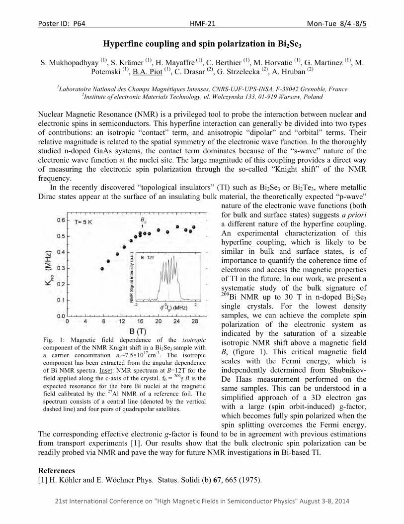
Poster ID: P64 HMF-‐21 Mon-‐Tue 8/4 -‐8/5
21st International Conference on "High Magnetic Fields in Semiconductor Physics" August 3-‐8, 2014
Hyperfine coupling and spin polarization in Bi2Se3
S. Mukhopadhyay (1), S. Krämer (1), H. Mayaffre (1), C. Berthier (1), M. Horvatic (1), G. Martinez (1), M. Potemski (1), B.A. Piot (1), C. Drasar (2), G. Strzelecka (2), A. Hruban (2)
1Laboratoire National des Champs Magnétiques Intenses, CNRS-UJF-UPS-INSA, F-38042 Grenoble, France
2Institute of electronic Materials Technology, ul. Wolczynska 133, 01-919 Warsaw, Poland
Nuclear Magnetic Resonance (NMR) is a privileged tool to probe the interaction between nuclear and electronic spins in semiconductors. This hyperfine interaction can generally be divided into two types of contributions: an isotropic “contact” term, and anisotropic “dipolar” and “orbital” terms. Their relative magnitude is related to the spatial symmetry of the electronic wave function. In the thoroughly studied n-doped GaAs systems, the contact term dominates because of the “s-wave” nature of the electronic wave function at the nuclei site. The large magnitude of this coupling provides a direct way of measuring the electronic spin polarization through the so-called “Knight shift” of the NMR frequency.
In the recently discovered “topological insulators” (TI) such as Bi2Se3 or Bi2Te3, where metallic Dirac states appear at the surface of an insulating bulk material, the theoretically expected “p-wave”
nature of the electronic wave functions (both for bulk and surface states) suggests a priori a different nature of the hyperfine coupling. An experimental characterization of this hyperfine coupling, which is likely to be similar in bulk and surface states, is of importance to quantify the coherence time of electrons and access the magnetic properties of TI in the future. In our work, we present a systematic study of the bulk signature of 209Bi NMR up to 30 T in n-doped Bi2Se3 single crystals. For the lowest density samples, we can achieve the complete spin polarization of the electronic system as indicated by the saturation of a sizeable isotropic NMR shift above a magnetic field Bs (figure 1). This critical magnetic field scales with the Fermi energy, which is independently determined from Shubnikov-De Haas measurement performed on the same samples. This can be understood in a simplified approach of a 3D electron gas with a large (spin orbit-induced) g-factor, which becomes fully spin polarized when the spin splitting overcomes the Fermi energy.
The corresponding effective electronic g-factor is found to be in agreement with previous estimations from transport experiments [1]. Our results show that the bulk electronic spin polarization can be readily probed via NMR and pave the way for future NMR investigations in Bi-based TI. References [1] H. Köhler and E. Wöchner Phys. Status. Solidi (b) 67, 665 (1975).
Fig. 1: Magnetic field dependence of the isotropic component of the NMR Knight shift in a Bi2Se3 sample with a carrier concentration ne~7.5×1017cm-3. The isotropic component has been extracted from the angular dependence of Bi NMR spectra. Inset: NMR spectrum at B=12T for the field applied along the c-axis of the crystal. f0 = 209γ B is the expected resonance for the bare Bi nuclei at the magnetic field calibrated by the 27Al NMR of a reference foil. The spectrum consists of a central line (denoted by the vertical dashed line) and four pairs of quadrupolar satellites.
Poster ID: P65 HMF-‐21 Mon-‐Tue 8/4 -‐8/5
21st International Conference on "High Magnetic Fields in Semiconductor Physics" August 3-‐8, 2014
Magnetotransport study of the ternary topological insulator (Bi0.5Sb0.5)2Te3 via in situ low temperature deposition of Cr
Liuqi Yu (1), Jorge Barreda (1), Longqian Hu (1), P. Xiong (1), Tong Guan (2), Xiaoyue He (2), K. Wu (2),
Y.Q. Li (2)
1Department of Physic, Florida State University, Tallahassee, USA 2Institution of Physics, Chinese Academy of Science, Beijing, China
The robustness of the surface state of three dimensional topological insulators against local magnetic perturbation is still under debate, since a precise and well-controlled electrical characterization of the effects of the ferromagnetic dopant and their evolution with doping density are exceedingly difficult. Here we report results of magnetotransport measurements on epitaxial thin films of the (Bi0.5Sb0.5)2Te3 in the presence of electrostatic gating and magnetic impurity. Magnetoresistance (MR) and Hall effect measurements have been performed in various back gate voltages. Ambipolar field effect has been observed, enabling effective tuning of the Fermi level across the band gap and identification of the surface transport in the topological transport regime. Taking advantage of the unique capability of in situ deposition of Cr atoms in a customized dilution refrigerator, magnetic impurities were incrementally quench-condensed onto the sample surface. The low-temperature Cr deposition yields an electron doping. The coherent transport of the topological surface state, to certain extent, is disturbed by the impurity deposition. However, in contrast to the current picture of gap opening at the Dirac point under strong spin-flip scattering, the weak antilocalization (WAL) effect was found to be surprisingly insensitive to the magnetic impurity; the cusp-like negative magnetoconductivity remains even at the highest Cr concentration and no apparent weak localization was observed as expected from a gap opening at the Dirac point. Our results suggest that the surface state could well stay in the symplectic case under randomized local magnetic scattering without long range ferromagnetic ordering. Work supported in part by NSF DMR-1308613.
Poster ID: P66 HMF-‐21 Mon-‐Tue 8/4 -‐8/5
21st International Conference on "High Magnetic Fields in Semiconductor Physics" August 3-‐8, 2014
Topological entanglement entropy in Z2 RVB quantum spin liquids
Julia Wildeboer1
1National High Magnetic Field Laboratory, Florida State University, Tallahassee, Florida 32310, USA
In this talk, I will summarizes our efforts made to calculate the topological entanglement entropy (TEE) (see for example Ref.[1]) of a wave function that describes a Z2 quantum spin liquid (QSL) on the kagome and the triangular lattice [2]. This wave function is of RVB-type.
More precisely, it is of ''Rokhsar-Kivelson'' form: here, the sum goes over all nearest-neighbor dimer coverings D of the respective lattice, and the state |D> is a realization of the dimer covering through products of singlet pairs, or ''valence bonds''. The wave function is then the equal amplitude superposition of all states |D>.
Details of the method (Paffian Monte Carlo, SWAP-operator formalism) used to calculate the TEE will be presented. Results will be presented on the QSL on the kagome and the triangular lattice. Additionally discussed will be the purported spin liquid phase in some contentious models, particularly J1-J2 square and honeycomb models. References [1] M. B. Hastings et. al., Phys. Rev. Lett. 104, 157201 (2010). [2] J. Wildeboer and A. Seidel, Phys. Rev. Lett. 109, 147208 (2012).
Poster ID: P67 HMF-‐21 Mon-‐Tue 8/4 -‐8/5
21st International Conference on "High Magnetic Fields in Semiconductor Physics" August 3-‐8, 2014
Single and double quantum dots at the edge of 2D topological insulator
A.A. Konakov, A.A. Chubanov, D.V. Khomitsky
University of Nizhniy Novgorod, Nizhniy Novgorod, Russia
Topological insulators remain to be among the hottest topics of both experimental and theoretical research in condensed matter physics during the last years [1, 2]. Existence of topologically protected current and spin-carrying states makes them promising for next generation of electronic devices. New types of confined states can also be formed there such as the states in quantum dots at the edge of quantum spin Hall insulators [3, 4]. In this work we develop theory of localized states at the quantum spin Hall edge produced by magnetic barriers with finite values of magnetization. First we consider single quantum dot (QD) formed at the edge of 2D topological insulator (TI). Free electrons at the quantum spin Hall state, such as HgTe quantum well with inverted band structure, are described by the Weyl Hamiltonian [1, 2]. One of the possible ways to confine massless Dirac fermions at the finite length L is creation of gapped barrier regions [5]. For electrons at the 2D TI edge it means that time reversal symmetry should be broken, i.e. magnetic barriers on the edge have to be formed. To localize electron into a single dot we assume that two magnetic barriers are positioned along the propagation direction of edge states. In the most general case absolute values and orientations of the magnetizations in barrier regions can be different. Taking into account only Zeeman energy of electron in barrier regions one can obtain the effective Hamiltonian of 2D TI QD with finite magnetic barriers, acting on the envelope function (in [3, 4] such Hamiltonian is presented for a case of impenetrable barriers). We calculated the electronic states in 2D TI QDs with different relations between absolute values and orientations of barriers’ magnetizations. In the case of symmetric barriers single-particle energies depend on the difference between magnetic fields’ directions in barriers. This fact opens a specific for discussed system possibility to manage electronic states: one can not only change a barrier height and QD size, but also manipulate relative orientation of the barriers’ magnetizations. When the magnetizations of the barriers have the same orientation, energy spectrum are symmetric with respect to the Dirac point. As opposed to “classical” quantum wells, where energy of the particle decreases as the second order of the well width, here the dependence on the QD size is smoother, just as L–1. We also calculated space distribution of spin density in the stationary states and found oscillations of their spin polarization as a function of the principal quantum number. Small energy spacing between levels in single dots and a wide range of their quantum engineering possibilities allow one to manipulate easily electronic states in double dots. Using the LCAO method we determined energy spectrum of the double QD depending on properties of the magnetic barrier between single dots. Our calculations are of a great interest for developing qubits based on the edge of 2D TI. The work was financially supported by RFBR (grants N 13-02-00717-a and 13-02-00784-a) and by the “Dynasty” Foundation.
References [1] M. Z. Hasan and C. L. Kane, Rev. Mod. Phys. 82, 3045 (2010). [2] X.-L. Qi and S.-C. Zhang, Rev. Mod. Phys. 83, 1057 (2011). [3] C. Timm, Phys. Rev. B 86, 155456 (2012). [4] G. Dolcetto et al., Phys. Rev. B 87, 235423 (2013). [5] M. I. Katsnelson, K. S. Novoselov, A. K. Geim, Nature Phys. 2, 620 (2006).

Poster ID: P68 HMF-‐21 Mon-‐Tue 8/4 -‐8/5
21st International Conference on "High Magnetic Fields in Semiconductor Physics" August 3-‐8, 2014
Magnetotransport of Topological Insulators
Yang Xu (1,2), Helin Cao (3), Ireneusz Miotkowski (1), Yong P. Chen (1,2,4)
1 Purdue University / Department of Physics and Astronomy, West Lafayette, IN 47907, USA
2 Purdue University / Birck Nanotechnology Center, West Lafayette, IN 47907, USA 3 University of Washington / Department of Physics, Seattle, WA 98195, USA
4 Purdue University / School of Electrical and Computer Engineering, West Lafayette, IN 47907, USA
A three-dimensional (3D) strong topological insulator (TI) has a fully insulating gap in the bulk and topological surface states (TSS) of gapless Dirac fermions. However it is a great challenge to separate and eliminate bulk conduction from surface conduction and reveal the transport signatures of the Dirac fermion from surface states in real 3D TI materials. By Bridgman method, we’ve successfully grown high-quality single crystalline TIs from highly-bulk-doped Bi2Se3 to bulk-insulating Bi2Te2Se (BTS221) and BiSbTeSe2 (BSTS). The Bi2Se3 is sufficiently highly doped in the bulk such that it exhibits a thickness-dependent bulk quantum Hall effect (QHE, displaying 2D-like Shubnikov-de Haas (SdH) oscillations, accompanied by a quantized Hall effect (QHE) associated with many parallel 2D electron systems attributed to electronically decoupled quintuple layers [1]). BTS221 and BSTS both
have large bulk resistivity and low bulk density at low temperature and we observed surface-dominated transport behavior. However, the surface transport can be from coexisting TSS and topological trivial 2D electron gas (2DES) in BTS221 (Fig. 1, exhibiting two sets of SdH oscillations with π and 0 phase respectively) [2]. In the most bulk insulating BSTS, we observed pure TSS transport and QHE from TSS emerges [3]. Our experiments reveal different magnetotransport behaviors due to bulk, trivial surface states (2DES from band bending), and topological surface states in 3D TI materials with different doping levels and pave the way for further application of topological quantum electronics.
We acknowledge support from DARPA MESO program (Grant N66001-11-1-4107). References [1] Cao, H. et al. Quantized Hall effect and Shubnikov--de Haas oscillations in highly doped Bi2Se3: Evidence for layered transport of bulk carriers. Phys. Rev. Lett. 108, 216803 (2012). [2] Cao, H. et al. submitted (2014). [3] Xu, Y. et al. submitted (2014).
Fig. 1: (a) Shubnikov–de Haas (SdH) oscillations arising from TSSs and trivial 2DES. Oscillatory component ∆Rxx, extracted from Rxx by subtracting a smooth polynomial background, is plotted against 1/B⊥ at various tilt angles (θ) measured in BTS221. (b) The Landau fan diagram fit of SdH oscillations. 2DES gives intercept 0, consistent with Schrödinger fermions and TSS gives ~0.5, indicating Dirac fermions.
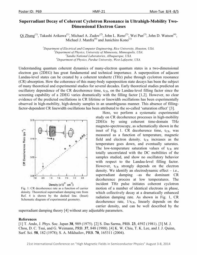
Poster ID: P69 HMF-‐21 Mon-‐Tue 8/4 -‐8/5
21st International Conference on "High Magnetic Fields in Semiconductor Physics" August 3-‐8, 2014
Superradiant Decay of Coherent Cyclotron Resonance in Ultrahigh-Mobility Two-Dimensional Electron Gases
Qi Zhang(1), Takashi Arikawa(1), Michael A. Zudov(2), John L. Reno(3), Wei Pan(3), John D. Watson(4),
Michael J. Manfra(4) and Junichiro Kono(1)
1Department of Electrical and Computer Engineering, Rice University, Houston, USA.
2Department of Physics, University of Minnesota, Minneapolis, USA. 3Sandia National Laboratories, Albuquerque, USA.
4Department of Physics, Purdue University, West Lafayette, USA.
Understanding quantum coherent dynamics of many-electron quantum states in a two-dimensional electron gas (2DEG) has great fundamental and technical importance. A superposition of adjacent Landau-level states can be created by a coherent terahertz (THz) pulse through cyclotron resonance (CR) absorption. How the coherence of this many-body superposition state decays has been the subject of many theoretical and experimental studies for several decades. Early theoretical studies predicted an oscillatory dependence of the CR decoherence time, τCR, on the Landau-level filling factor since the screening capability of a 2DEG varies dramatically with the filling factor [1,2]. However, no clear evidence of the predicted oscillations in CR lifetime or linewidth oscillations has been experimentally observed in high-mobility, high-density samples in an unambiguous manner. This absence of filling-factor-dependent CR linewidth oscillations has been attributed to the so-called ‘saturation effect’ [3].
Here, we perform a systematic experimental study on CR decoherence processes in high-mobility 2DEGs by using coherent time-domain THz magneto-spectroscopy, as schematically shown in the inset of Fig. 1. CR decoherence time, τCR, was measured as a function of temperature, magnetic field and electron density. τCR increases as the temperature goes down, and eventually saturates. The low-temperature saturation values of τCR are totally uncorrelated with the DC mobilities of the samples studied, and show no oscillatory behavior with respect to the Landau-level filling factor. However, τCR strongly depends on the electron density. We identify an electrodynamic effect – i.e., superradiant damping –as the dominant CR decoherence process at low temperatures. The incident THz pulse initiates coherent cyclotron motion of a number of identical electrons in phase, which collectively decay at a dramatically enhanced radiation damping rate. As shown in Fig. 1, CR decoherence rate, 1/τCR, linearly depends on the carrier density, and can be well described by the
superradiant damping theory [4] without any adjustable parameters. References [1] T. Ando, J. Phys. Soc. Japan 38, 989 (1975). [2] S. Das Sarma, PRB. 23, 4592 (1981). [3] M. J. Chou, D. C. Tsui, and G. Weimann, PRB. 37, 848 (1988). [4] K. W. Chiu, T. K. Lee, and J. J. Quinn, Surf. Sci. 58, 182 (1978); S. A. Mikhailov, PRB. 70, 165311 (2004).
Fig. 1: CR decoherence rate as a function of carrier density. Theoretical superradiant damping rate from Ref. 4 is shown by the dashed line. (Inset) Schematic diagram of experimental geometry.

Poster ID: P70 HMF-21 Tue 8/5
21st International Conference on "High Magnetic Fields in Semiconductor Physics" August 3-8, 2014
Theory of evolution of recombination spectra of 2D electrons in a high magnetic field as a function of carrier density
M. Korkusinski (1), P. Hawrylak (1)
1Quantum Theory Group, Security and Disruptive Technologies Portfolio, National Research Council, Ottawa, Canada
Motivated by recent experiments [1,2] we present theory of evolution of the polarization-resolved recombination spectra of 2D electrons in a high magnetic field as a function of carrier density controlled by the external gate. The initial photoexcited system consists of N electrons and an exciton while the final state consists of N electrons on the Haldane sphere. Varying N allows to follow the evolution of the emission spectra for the �+ and �� polarizations from exciton, trion to filling factor �>1/3 at a constant magnetic field. Unexpected quenching of emission for �~1/4 is observed.
We generate all spin-resolved lowest-Landau-level configurations of N+1 electrons and one hole (initial state) and N electrons (final state in emission) for a given 2S. Weaker electron-hole interactions introduce breaking of hidden symmetry. In the basis of ~105 configurations the Hamiltonian matrix is created and diagonalized numerically using the iterative block conjugate gradient algorithm. The polarization-resolved emission spectra are computed as a function of N using the Fermi’s Golden Rule [2,3].
Figure 1 shows the emission spectra as a function of N for 2S=12. Starting with the neutral exciton X, the main features, corresponding to the majority spin recombination σ-, shift towards lower energies due to increasing exchange energy. For N=5 (filling factor ν=1/3) we reproduce the emission of the charged quasiexciton in the incompressible fluid, and for N=6 (ν=1/3+) we observe broadening due to the fractionally charged quasiexciton reported previously [2,3]. However, in each case we see additional maxima with σ+ at a slightly higher energy due to the thermal population of a N+X spin-depolarized state. The energy gap between the lowest σ- and σ+ polarized peaks defines the binding energy of the fractionally charged quasiexciton. For N=4 (ν=1/4) the low-lying states of the photoexcited system are dark and the emission spectra are quenched. The quenching of emission at ν=1/4 is also reproduced for N=5 and 2S=16.
Work in collaboration with S. Nomura, M. Yamaguchi, H. Tamura, T. Akazaki, and Y. Hirayama. References [1] S. Nomura, M. Yamaguchi, H. Tamura, T. Akazaki, Y. Hirayama, M. Korkusinski, and P. Hawrylak, Phys. Rev. B (in press); G. Yusa, H. Shtrikman, and I. Bar-Joseph, Phys. Rev. Lett. 87, 216402 (2001). [2] M. Byszewski, B. Chwalisz, D. Maude, M. Sadowski, M. Potemski, T. Saku, Y. Hirayama, S. Studenikin, D. G. Austing, A. Sachrajda, and P. Hawrylak, Nature Phys. 2, 239 (2006). [3] A. Wojs, A. Gladysiewicz and J. J. Quinn, Phys. Rev. B 73, 235338 (2006).
-2.5 -2.0 -1.5 -1.0
0.000
0.005
0.010
0.015
0.020
x 0.05
x 0.005
x 0.0005
6e+X
5e+X
4e+X
3e+X
2e+X
1e+X
X
Am
plitu
de (
arb.
u.)
Energy (Eg)
Fig. 1: Emission spectra of the N+X system as a function of the number N of carriers for 2S=12.
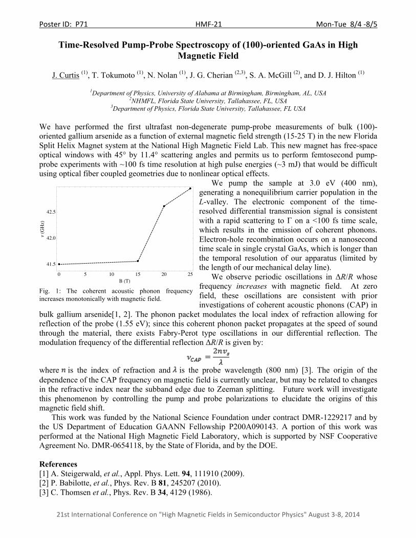
Poster ID: P71 HMF-‐21 Mon-‐Tue 8/4 -‐8/5
21st International Conference on "High Magnetic Fields in Semiconductor Physics" August 3-‐8, 2014
Time-Resolved Pump-Probe Spectroscopy of (100)-oriented GaAs in High Magnetic Field
J. Curtis (1), T. Tokumoto (1), N. Nolan (1), J. G. Cherian (2,3), S. A. McGill (2), and D. J. Hilton (1)
1Department of Physics, University of Alabama at Birmingham, Birmingham, AL, USA
2NHMFL, Florida State University, Tallahassee, FL, USA 3Department of Physics, Florida State University, Tallahassee, FL USA
We have performed the first ultrafast non-degenerate pump-probe measurements of bulk (100)-oriented gallium arsenide as a function of external magnetic field strength (15-25 T) in the new Florida Split Helix Magnet system at the National High Magnetic Field Lab. This new magnet has free-space optical windows with 45° by 11.4° scattering angles and permits us to perform femtosecond pump-probe experiments with ~100 fs time resolution at high pulse energies (~3 mJ) that would be difficult using optical fiber coupled geometries due to nonlinear optical effects.
We pump the sample at 3.0 eV (400 nm), generating a nonequilibrium carrier population in the L-valley. The electronic component of the time-resolved differential transmission signal is consistent with a rapid scattering to Γ on a <100 fs time scale, which results in the emission of coherent phonons. Electron-hole recombination occurs on a nanosecond time scale in single crystal GaAs, which is longer than the temporal resolution of our apparatus (limited by the length of our mechanical delay line). We observe periodic oscillations in ΔR/R whose frequency increases with magnetic field. At zero field, these oscillations are consistent with prior investigations of coherent acoustic phonons (CAP) in
bulk gallium arsenide[1, 2]. The phonon packet modulates the local index of refraction allowing for reflection of the probe (1.55 eV); since this coherent phonon packet propagates at the speed of sound through the material, there exists Fabry-Perot type oscillations in our differential reflection. The modulation frequency of the differential reflection ΔR/R is given by:
where is the index of refraction and is the probe wavelength (800 nm) [3]. The origin of the dependence of the CAP frequency on magnetic field is currently unclear, but may be related to changes in the refractive index near the subband edge due to Zeeman splitting. Future work will investigate this phenomenon by controlling the pump and probe polarizations to elucidate the origins of this magnetic field shift. This work was funded by the National Science Foundation under contract DMR-1229217 and by the US Department of Education GAANN Fellowship P200A090143. A portion of this work was performed at the National High Magnetic Field Laboratory, which is supported by NSF Cooperative Agreement No. DMR-0654118, by the State of Florida, and by the DOE. References [1] A. Steigerwald, et al., Appl. Phys. Lett. 94, 111910 (2009). [2] P. Babilotte, et al., Phys. Rev. B 81, 245207 (2010). [3] C. Thomsen et al., Phys. Rev. B 34, 4129 (1986).
ÊÊ
Ê
Ê
0 5 10 15 20 25
41.5
42.0
42.5
B HTL
nHGH
zL
Fig. 1: The coherent acoustic phonon frequency increases monotonically with magnetic field.
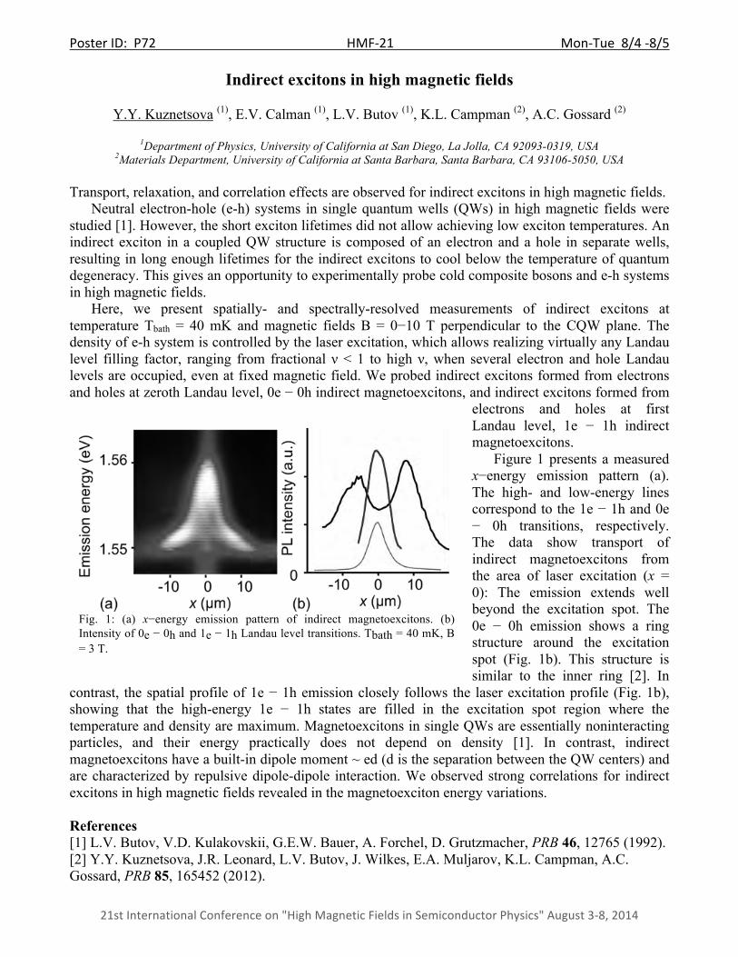
Poster ID: P72 HMF-‐21 Mon-‐Tue 8/4 -‐8/5
21st International Conference on "High Magnetic Fields in Semiconductor Physics" August 3-‐8, 2014
Indirect excitons in high magnetic fields
Y.Y. Kuznetsova (1), E.V. Calman (1), L.V. Butov (1), K.L. Campman (2), A.C. Gossard (2)
1Department of Physics, University of California at San Diego, La Jolla, CA 92093-0319, USA 2Materials Department, University of California at Santa Barbara, Santa Barbara, CA 93106-5050, USA
Transport, relaxation, and correlation effects are observed for indirect excitons in high magnetic fields. Neutral electron-hole (e-h) systems in single quantum wells (QWs) in high magnetic fields were studied [1]. However, the short exciton lifetimes did not allow achieving low exciton temperatures. An indirect exciton in a coupled QW structure is composed of an electron and a hole in separate wells, resulting in long enough lifetimes for the indirect excitons to cool below the temperature of quantum degeneracy. This gives an opportunity to experimentally probe cold composite bosons and e-h systems in high magnetic fields. Here, we present spatially- and spectrally-resolved measurements of indirect excitons at temperature Tbath = 40 mK and magnetic fields B = 0−10 T perpendicular to the CQW plane. The density of e-h system is controlled by the laser excitation, which allows realizing virtually any Landau level filling factor, ranging from fractional ν < 1 to high ν, when several electron and hole Landau levels are occupied, even at fixed magnetic field. We probed indirect excitons formed from electrons and holes at zeroth Landau level, 0e − 0h indirect magnetoexcitons, and indirect excitons formed from
electrons and holes at first Landau level, 1e − 1h indirect magnetoexcitons. Figure 1 presents a measured x−energy emission pattern (a). The high- and low-energy lines correspond to the 1e − 1h and 0e − 0h transitions, respectively. The data show transport of indirect magnetoexcitons from the area of laser excitation (x = 0): The emission extends well beyond the excitation spot. The 0e − 0h emission shows a ring structure around the excitation spot (Fig. 1b). This structure is similar to the inner ring [2]. In
contrast, the spatial profile of 1e − 1h emission closely follows the laser excitation profile (Fig. 1b), showing that the high-energy 1e − 1h states are filled in the excitation spot region where the temperature and density are maximum. Magnetoexcitons in single QWs are essentially noninteracting particles, and their energy practically does not depend on density [1]. In contrast, indirect magnetoexcitons have a built-in dipole moment ~ ed (d is the separation between the QW centers) and are characterized by repulsive dipole-dipole interaction. We observed strong correlations for indirect excitons in high magnetic fields revealed in the magnetoexciton energy variations. References [1] L.V. Butov, V.D. Kulakovskii, G.E.W. Bauer, A. Forchel, D. Grutzmacher, PRB 46, 12765 (1992). [2] Y.Y. Kuznetsova, J.R. Leonard, L.V. Butov, J. Wilkes, E.A. Muljarov, K.L. Campman, A.C. Gossard, PRB 85, 165452 (2012).
Fig. 1: (a) x−energy emission pattern of indirect magnetoexcitons. (b) Intensity of 0e − 0h and 1e − 1h Landau level transitions. Tbath = 40 mK, B = 3 T.
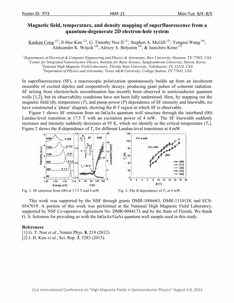
Poster ID: P73 HMF-‐21 Mon-‐Tue 8/4 -‐8/5
21st International Conference on "High Magnetic Fields in Semiconductor Physics" August 3-‐8, 2014
Magnetic field, temperature, and density mapping of superfluorescence from a quantum-degenerate 2D electron-hole system
Kankan Cong (1), Ji-Hee Kim (2), G. Timothy Noe II (1), Stephen A. McGill (3), Yongrui Wang (4),
Aleksander K. Wójcik (4), Alexey A. Belyanin (4), & Junichiro Kono (1)
1Departments of Electrical & Computer Engineering and Physics & Astronomy, Rice University, Houston, TX 77005, USA
2Center for Integrated Nanostructure Physics, Institute for Basic Science, Sungkyunkwan University, Suwon, Korea 3National High Magnetic Field Laboratory, Florida State University, Tallahassee, FL 32310, USA 4Department of Physics and Astronomy, Texas A&M University, College Station, TX 77843, USA
In superfluorescence (SF), a macroscopic polarization spontaneously builds up from an incoherent ensemble of excited dipoles and cooperatively decays, producing giant pulses of coherent radiation. SF arising from electron-hole recombination has recently been observed in semiconductor quantum wells [1,2], but its observability conditions have not been fully understood. Here, by mapping out the magnetic field (B), temperature (T), and pump power (P) dependence of SF intensity and linewidth, we have constructed a ‘phase’ diagram, showing the B-T region in which SF is observable.
Figure 1 shows SF emission from an InGaAs quantum well structure through the interband (00) Landau-level transition at 17.5 T with an excitation power of 4 mW. The SF linewidth suddenly increases and intensity suddenly decreases at 95 K, which we identify as the critical temperature (Tc). Figure 2 shows the B-dependence of Tc for different Landau-level transitions at 4 mW.
Fig. 1: SF emission from (00) at 17.5 T and 4 mW. Fig. 2: The B-dependence of Tc at 4 mW.
This work was supported by the NSF through grants DMR-1006663, DMR-1310138, and ECS-0547019. A portion of this work was performed at the National High Magnetic Field Laboratory, supported by NSF Co-operative Agreement No. DMR-0084173 and by the State of Florida. We thank G. S. Solomon for providing us with the InGaAs/GaAs quantum well sample used in this study. References [1] G. T. Noe et al., Nature Phys. 8, 219 (2012). [2] J. H. Kim et al., Sci. Rep. 3, 3283 (2013).

Poster ID: P74 HMF-‐21 Mon-‐Tue 8/4 -‐8/5
21st International Conference on "High Magnetic Fields in Semiconductor Physics" August 3-‐8, 2014
Giant Zeeman Splitting in Submonolayer ZnTe/ZnSe Quantum Dots
H. Ji,1, 3,* S. Dhomkar,1, 3 J. Ludwig,4 D. Smirnov,4 M. C. Tamargo,2, 3 and I. L. Kuskovsky1, 3
1Department of Physics, Queens College of CUNY, Queens, NY 11367
2Department of Chemistry, City College of CUNY, New York, NY 10031 3The Graduate Center of CUNY, New York, NY 10016
4National High Magnetic Field Laboratory, Tallahassee, FL 32310 *[email protected]
Having the type-II band alignment and large valence band offset, the ZnTe/ZnSe quantum dots (QDs) have attracted interest in applications of optoelectronic and photonic devices. For the application purposes as well as for understanding the underlying physics, the study of magnetic g-factor and Zeeman splitting of excitons is important because it provides insights into subband structure, spin-orbit interaction, and mixing between exciton states. Here we report the giant Zeeman splitting observed in the circularly polarized magneto-photoluminescence (PL) of submonolayer ZnTe/ZnSe QDs grown using migration enhanced epitaxy. The exciton g-factors obtained are unusually large for non-magnetic semiconductors.
Circularly polarized magneto-PL up to 18 Tesla was measured on two samples. Sample A is grown using higher Te flux than sample B [1]. The magnetic field dependences of Zeeman splitting, ΔE, of the σ+ and σ- emission energies are shown in Fig. 1. Fitting the data to the equation , where gex is the effective exciton g-factor, µB is the Bohr magneton, and B is applied magnetic field, we obtain exciton gex ≈ 14 for sample A and gex ≈ 32 for sample B, which are much larger than the values reported for bulk ZnSe and ZnTe systems [2, 3]. We attribute these giant exciton g-factors to mostly the strong quantum confinement of the holes in ZnTe QDs [4, 5]. The fact that the exciton g-factor in sample B is larger than that in sample A, is due to the smaller QD sizes, and therefore larger quantum confinement effects. The vertical – in growth direction – confinement is estimated from the type-II exciton emission energy, while the lateral one is from transition magnetic field of the Aharonov-Bohm excitons [1]. Using these estimates, we show that lateral confinement contribution is still significant even though it is much smaller than that in growth direction. References [1] H. Ji, et al., J. Electron. Mater. 42, 3297 (2013) [2] G. V. Astakhov, et al., Phys. Rev. B 65, 165335 (2002) [3] H. Venghaus and B. Jusserand, Phys. Rev. B 22, 932 (1980) [4] M. J. Snelling, et al., Phys. Rev. B 45, 3922 (1992) [5] T. Gutbrod, et al., Phys. Stat. Sol. (a) 164, 409 (1997)
Figure 1: Zeeman splitting of the σ+ and σ- emission energies as a function of the magnetic field.

Poster ID: P75 HMF-‐21 Mon-‐Tue 8/4 -‐8/5
21st International Conference on "High Magnetic Fields in Semiconductor Physics" August 3-‐8, 2014
Exchange interaction between carrier and single Mn2+ ion: comparison of CdTe and CdSe quantum dots
T. Smolenski (1), W. Pacuski (1), M. Goryca (1), J. Kobak (1), M. Koperski (1), J.-G. Rousset (1),
A. Golnik (1), M. Nawrocki (1), M. Potemski (2), and P. Kossacki (1)
1Institute of Experimental Physics, Faculty of Physics, University of Warsaw, Warsaw, Poland 2Laboratoire National des Champs Magnétiques Intenses, CNRS-UJF-UPS-INSA, Grenoble, France
Semiconductor quantum dot (QD) with a single magnetic ion is a model system for spectroscopic studies of exchange interaction between individual ion and confined carriers [1]. It offers a range of unique functionalities, e.g., an optical control over the ion spin state. However, the studies of such dots were severely limited by a common belief that exciton photoluminescence (PL) is quenched by magnetic ion when the exciton energy is higher than the intra-ionic transition energy. As a result, the only QDs with single magnetic dopants explored so far were CdTe/ZnTe and InAs/GaAs QDs embedding Mn2+ ions. Recently, it has been shown that magnetic-ion-related quenching, even if energetically allowed, is negligible for a QD with an individual ion [2]. This finding extended the optical studies of such QDs for a wide group of systems. Here we report on a magneto-spectroscopic study of electron and hole exchange interaction with a single Mn2+ ion in CdSe QDs. The presence of such interaction induces a sixfold splitting of neutral exciton (X) emission line [1-3]. The evolution of X PL spectrum in high magnetic field measured in Faraday configuration (Fig. 1a) is analyzed within the frame of a theoretical model described in [1,2] (Fig. 1b). On this basis we determine both the electron-ion and hole-ion exchange integrals, as well as the excitonic diamagnetic shift. Their values are compared with the respective parameters obtained for previously studied CdTe QDs embedding the same Mn2+ ions [3]. Diamagnetic shift in the case of CdSe QDs is found to be a few times lower. It yields a smaller spatial extension of the excitonic wave function. Simultaneously, similar s,p-d exchange constants N0α and N0β for bulk CdSe and CdTe suggest a larger carrier-ion exchange integrals in the case of CdSe dots. In contrast, the experimentally obtained integrals for several CdSe QDs are not exceeding typical values determined for CdTe QDs. Moreover, the electron-ion exchange integral for CdSe QDs is particularly low yielding a large ratio of hole-ion and electron-ion integrals exceeding 30 compared to |N0β/N0α|≈5.5. This findings might be interpreted as a result of non-central localization of Mn2+ ion in a CdSe dot. In such case, the density of strongly confined electron wave function at the position of the ion can be significantly lower compared to a density of delocalized wave function of the hole.
References [1] L. Besombes et al., Phys. Rev. Lett. 93, 207403 (2004). [2] J. Kobak, T. Smolenski et al., Nature Communications 5, 3191 (2014). [3] M. Koperski et al., Phys. Rev. B 89, 075311 (2014).
Fig. 1: (a) Experimental and (b) simulated PL spectrum of an exciton in a CdSe/ZnSe QD with a single Mn2+ ion as a function of magnetic field in Faraday configuration.
Poster ID: P76 HMF-‐21 Mon-‐Tue 8/4 -‐8/5
21st International Conference on "High Magnetic Fields in Semiconductor Physics" August 3-‐8, 2014
Terahertz Time-Domain Magnetospectroscopy Using a 30 T Table-Top Repetitive Pulsed Magnet
G. T. Noe (1), Q. Zhang (1), J. Lee (1), E. Kato (2), G. L. Woods (1), H. Nojiri (3), J. Kono (1)
1Department of Electrical and Computer Engineering, Rice University, Houston, Texas, USA
2Advantest America, Inc., Princeton, New Jersey, USA 3Institute for Materials Research, Tohoku University, Sendai, Japan
We have performed terahertz time-domain spectroscopy at the peak of the magnetic field generated by a mini-coil pulsed magnet capable of producing magnetic fields up to 30 T by coupling the mini-coil magnet with a rapid scanning electronically controlled optical sampling (ECOPS) based terahertz time-domain spectroscopy (THz-TDS) setup. Combining THz-TDS with high magnetic fields can provide information about low-energy excitations in solids, of both spin and orbital origins. Recently, we have developed a magneto-optical system specifically for ultrafast and nonlinear spectroscopy with solids in high, pulsed magnetic fields with sample temperatures down to ~10 K [1]. Here, we demonstrate the ability to efficiently measure a THz waveform at the peak of the magnetic field generated with our pulsed magnet. The ECOPS method for time-resolved spectroscopy utilizes two lasers with slightly different repetition rates where one laser beam is used for the pump and the other laser beam is used for the probe. The time delay between the pump and probe is scanned without the use of a mechanical delay stage. In a THz-TDS system, one beam is used for the generation of THz radiation and the other is used to probe or measure
the THz electric field. Figure 1 shows the synchronization of the THz waveform with the peak of the magnetic field pulse. A single sweep THz waveform is recorded at the peak of the magnetic field where the magnetic field variation is relatively constant (less than 1%) in the time between the main pulse and the reflection from the back side of the sample. Here, 150 µs of measurement time corresponds to 15 ps of time delay. We demonstrate the utility of this type of setup by measuring coherent cyclotron resonance (CCR) oscillations in a two-dimensional electron gas (2DEG) sample and transmission modulation in bulk n-InSb similar to previous studies [3,4].
References [1] G. T. Noe et al., Rev. Sci. Instrum. 84, 123906 (2013). [2] G. T. Noe et al., arXiv:1404.5592 (2014). [3] X. Wang et al., Opt. Lett. 32, 1845 (2007). [4] X. Wang et al., Nat. Phys. 6, 126 (2010).
Fig. 1: Synchronization of THz waveform with the peak of the generated magnetic field [2].