what are some of the common classes of leaded packages?
TRANSCRIPT

1
SM Platform Product Team
Best Practices 51030001, Rev. C
Leaded Application Notes
What are some of the common classes of leaded packages?
Descriptions Views
Small Outline Transistor (SOT) - A plastic leaded component in which transistors are packaged.
Plastic Leaded Chip Carrier (PLCC) - Normally a four-sided quad package in which an IC is installed with J-type leads extending out from the sides of the package then down and rolled under the body of the device.
Small Outlined Integrated Circuit (SOIC) – A small dual in-line package that has gull-wing shaped leads.
Thin Small Outline Package (TSOP) - Similar to SOIC but smaller packaging and closer lead spacing (8 to 24 leads) with leads protruding from the ends of the package.
Quad Flat Pack (QFP) - Four-sided device normally with extended gull-wing leads.

2
In general terms, how does the algorithm work? The algorithm uses image processing to determine the center point of each lead on a per lead group basis. It then performs a best fit for each lead group by using the programmed model data for that given lead group only.
Where is the lead type configured? How many different lead types are there? The Lead Type is found on the Leads tab of the component definition.
Currently, there are five lead choices:
1. Gull Wing 2. J Bend 3. UIC A 4. UIC B 5. UIC C
Assigned center points using high speed or standard accuracy.
Finally, the component location is generated by using the center points from all of the lead groups.

3
Lead Type Description Examples
Gull Wing: Finds lead tips and is commonly used for gull-wing component types (QFP, SOIC, etc.).
J Bend: Finds lead centers and is commonly used for J-type components (PLCC, SOJ, etc.).
One Lead: This lead type is optimized for components with one lead per lead group, such as e-caps and crystal oscillators.
E-Cap
UIC A: Finds lead tips and is typically used for components whose leads have non-uniform reflectivity. This lead type is also more geometrically tolerant than the gull-wing lead type (i.e. more tolerant to slightly bent leads).
UIC B: The same as UIC-A except this algorithm finds the inside tips and is also known as "inverted lead find".
Crystal

4
Lead Type Description Examples
UIC C: Finds lead tips, but used for components with very large leads that take up more than 25 pixels in width on the camera.
Large Leads
How do I convert my lead dimensions into pixels? Divide each lead dimension (in global units) by the camera resolution (in global units per pixel). For example, say we have the following data:
• Camera resolution = 2 mils/pixel • Lead width = 14 mils • Lead length = 24 mils
Lead width = 14 mils / 2 mils/pixel = 7 pixels Lead length = 24 mils / 2 mils/pixel = 12 pixels NOTE: 1 mil = 1 thousandth (10-3) of an inch What does Inspection Type mean? The Inspection Type is found on the Vision tab of the component definition.
There are two choices: High Accuracy High Speed
From the perspective of the leaded algorithm, the Inspection Type determines if additional image processing is used to center the component. The image on page 2 corresponds to High Speed.

5
The image below depicts High Accuracy centering. With High Accuracy centering, the algorithm will revise the center points by using grayscale rulers for each lead on a per lead group basis.
What are the advantages and disadvantages to high accuracy? Advantages:
• More accurate placements • Sometimes can be used to find leads that were labeled as missing with
High Speed Disadvantages:
• Slower, particularly on the 630 and older vision systems When should High Accuracy be used? High Accuracy processing is generally used for fine pitch components that are configured for lead inspection. When should lead inspection be used? Lead inspection is typically used with fine pitch components where an extra level of checking is required to ensure that the leads are not bent or otherwise damaged. It is typically not used for robust course pitch components that are packaged and handled in such a way to preclude lead damage.
New center points using high accuracy.
6
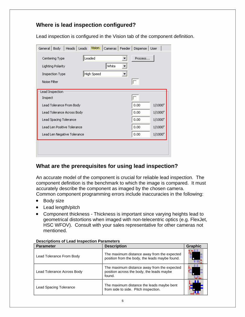
Where is lead inspection configured? Lead inspection is configured in the Vision tab of the component definition.
What are the prerequisites for using lead inspection? An accurate model of the component is crucial for reliable lead inspection. The component definition is the benchmark to which the image is compared. It must accurately describe the component as imaged by the chosen camera. Common component programming errors include inaccuracies in the following: • Body size • Lead length/pitch • Component thickness - Thickness is important since varying heights lead to
geometrical distortions when imaged with non-telecentric optics (e.g. FlexJet, HSC WFOV). Consult with your sales representative for other cameras not mentioned.
Descriptions of Lead Inspection Parameters Parameter Description Graphic
Lead Tolerance From Body The maximum distance away from the expected position from the body, the leads maybe found.
Lead Tolerance Across Body The maximum distance away from the expected position across the body, the leads maybe found.
Lead Spacing Tolerance The maximum distance the leads maybe bent from side to side. Pitch inspection.
7
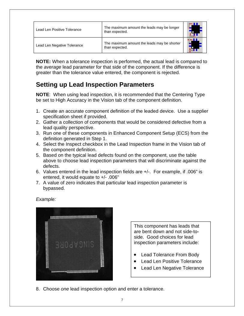
Lead Len Positive Tolerance The maximum amount the leads may be longer than expected.
Lead Len Negative Tolerance The maximum amount the leads may be shorter than expected.
NOTE: When a tolerance inspection is performed, the actual lead is compared to the average lead parameter for that side of the component. If the difference is greater than the tolerance value entered, the component is rejected. Setting up Lead Inspection Parameters NOTE: When using lead inspection, it is recommended that the Centering Type be set to High Accuracy in the Vision tab of the component definition. 1. Create an accurate component definition of the leaded device. Use a supplier
specification sheet if provided. 2. Gather a collection of components that would be considered defective from a
lead quality perspective. 3. Run one of these components in Enhanced Component Setup (ECS) from the
definition generated in Step 1. 4. Select the Inspect checkbox in the Lead Inspection frame in the Vision tab of
the component definition. 5. Based on the typical lead defects found on the component, use the table
above to choose lead inspection parameters that will discriminate against the defects.
6. Values entered in the lead inspection fields are +/-. For example, if .006” is entered, it would equate to +/- .006”
7. A value of zero indicates that particular lead inspection parameter is bypassed.
Example:
8. Choose one lead inspection option and enter a tolerance.
This component has leads that are bent down and not side-to-side. Good choices for lead inspection parameters include: • Lead Tolerance From Body • Lead Len Positive Tolerance • Lead Len Negative Tolerance

8
9. Inspect the component in ECS and note the displayed MAX DEVIATION. This is the deviation of the chosen inspection observed by the vision system (units are in microns). Since this is a part that should fail lead inspection, adjust the corresponding tolerance to be smaller than the MAX_DEVIATION. Record the tolerance.
10. Repeat this process for each of the chosen lead inspection parameters separately.
11. When finished, re-enter all of the tolerances determined in Steps 6-7 and test the component definition with other “bad” components as well as “good” components.
12. Refine the tolerances as necessary to ensure that the definition passes high quality components and fails components with unacceptable lead damage.
NOTE: Lead inspections are performed sequentially in the order listed in the component database. If an early inspection fails, no further inspections are performed. Are there any alternate methods for setting up lead inspection? Yes, the lead inspection parameters can also be setup based on pad size and required coverage.
9
What are some of the potential problems with the leaded algorithm?
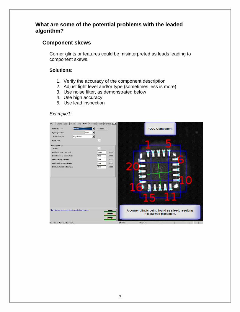
Component skews
Corner glints or features could be misinterpreted as leads leading to component skews. Solutions:
1. Verify the accuracy of the component description 2. Adjust light level and/or type (sometimes less is more) 3. Use noise filter, as demonstrated below 4. Use high accuracy 5. Use lead inspection
Example1:
10
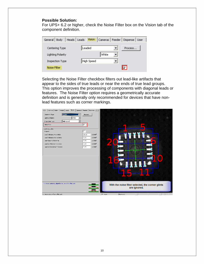
Possible Solution: For UPS+ 6.2 or higher, check the Noise Filter box on the Vision tab of the component definition.
Selecting the Noise Filter checkbox filters out lead-like artifacts that appear to the sides of true leads or near the ends of true lead groups. This option improves the processing of components with diagonal leads or features. The Noise Filter option requires a geometrically accurate definition and is generally only recommended for devices that have non-lead features such as corner markings.
11
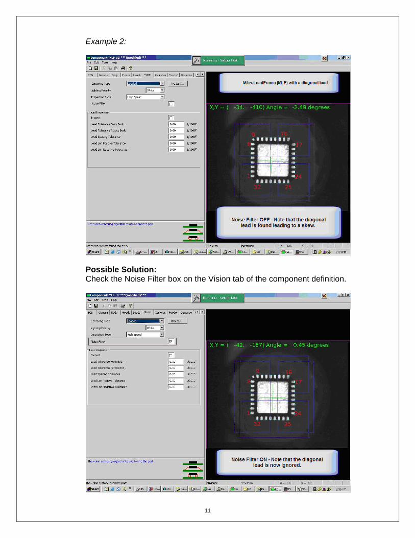
Example 2:
Possible Solution: Check the Noise Filter box on the Vision tab of the component definition.

12
Troubleshooting Tips for Component Failures
Always start your investigation by verifying the accuracy of the component description. This can be done through Enhanced Component Setup (ECS) from within the component definition. For more information on how to use this tool, refer to the online Help system.
This component description is incorrect, the lead pitch and component dimensions (length & width) need adjusting.
This component description is correct.
13
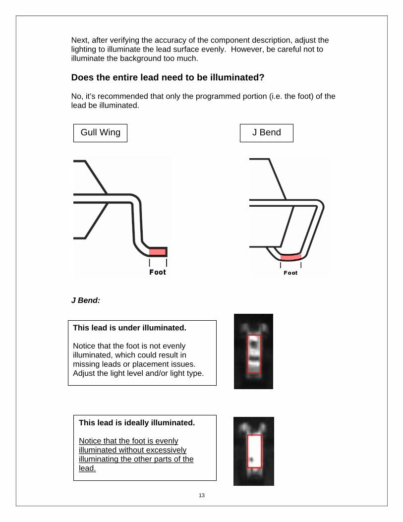
Next, after verifying the accuracy of the component description, adjust the lighting to illuminate the lead surface evenly. However, be careful not to illuminate the background too much. Does the entire lead need to be illuminated? No, it’s recommended that only the programmed portion (i.e. the foot) of the lead be illuminated.
J Bend:
Gull Wing J Bend
This lead is under illuminated. Notice that the foot is not evenly illuminated, which could result in missing leads or placement issues. Adjust the light level and/or light type.
This lead is ideally illuminated. Notice that the foot is evenly illuminated without excessively illuminating the other parts of the lead.

14
Gull Wing:
NOTE: On-Axis lighting is recommended for palladium leads.
This lead is over illuminated. Notice that the entire lead is over illuminated, which could result in missing leads or placement issues. Adjust the light level and/or light type.
This lead is under illuminated. Notice that the foot is not illuminated, which could result in missing leads or placement issues. Adjust the light level and/or light type.
This lead is ideally illuminated. Notice that the foot is evenly illuminated without excessively illuminating the other parts of the lead.
This lead is over illuminated. Notice that the entire lead is over illuminated, which could result in missing leads or placement issues. Adjust the light level and/or light type.
15
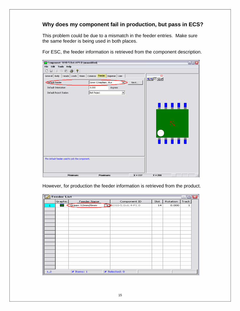
Why does my component fail in production, but pass in ECS? This problem could be due to a mismatch in the feeder entries. Make sure the same feeder is being used in both places. For ESC, the feeder information is retrieved from the component description.
However, for production the feeder information is retrieved from the product.

16
Another potential problem is with the inspection angle. Depending on the lead finish and camera type, some leads illuminate better in one orientation than another.
Check for this problem by inspecting the component in both orientations within ECS.
Try the following suggestions to avoid this problem. • Adjust lighting • Turn off pre-orient • Use a different camera type, preferably one with true on-axis lighting (e.g.
the Magellan ULC)
Change the Inspect Angle to rotate the component. NOTE: The component must be repicked for the new inspect angle to take effect.