whisker & hillock formation on sn, sn-cu and sn-pb ...wjb/whiskers and hillock.pdf · phosphor...
TRANSCRIPT

Whisker & Hillock Formation on Sn, Sn-Cu and Sn-Pb Electrodeposits
W. J. Boettinger*, C. E. Johnson, L. A. Bendersky, K.-W. Moon,
M. E. Williams and G. R. Stafford Metallurgy Division
NIST Gaithersburg, MD 20899
Friday, July 08, 2005
Abstract High purity bright Sn, Sn-Cu and Sn-Pb layers, 3, 7 and 16 µm thick were electrodeposited on
phosphor bronze cantilever beams in a rotating disk apparatus. Beam deflection
measurements within 15 min of plating proved that all electrodeposits had in-plane
compressive stress. In several days, the surfaces of the Sn-Cu deposits, which have the highest
compressive stress, develop 50 µm contorted hillocks and 200 µm whiskers, pure Sn deposits
develop 20 µm compact conical hillocks, and Sn-Pb deposits, which have the lowest
compressive stress, remain unchanged. The differences between the initial compressive
stresses for each alloy and pure Sn is due to the rapid precipitation of Cu6Sn5 or Pb particles,
respectively, within supersaturated Sn grains produced by electrodeposition. Over longer
time, analysis of beam deflection measurements indicates that the compressive stress is
augmented by the formation of Cu6Sn5 on the bronze/Sn interface, while creep of the
electrodeposit tends to decrease the compressive stress. Uniform creep occurs for Sn-Pb
because it has an equiaxed grain structure. Localized creep in the form of hillocks and
whiskers occurs for Sn and Sn-Cu because both have columnar structures. Compact hillocks
form for the Sn deposits because the columnar grain boundaries are mobile. Contorted
hillocks and whiskers form for the Sn-Cu deposits because the columnar grain boundary
motion is impeded.
Key Words: whiskers, electroplating, creep, grain boundary diffusion, solder.
* email: [email protected]

1. Introduction
Sn whiskers have been an industrial concern and interesting problem for many years. They are
known to cause short circuits in fine pitch pretinned electrical components. In contrast to
many whisker growth processes, Sn whiskers grow by the addition of material at their base
not at their tip; i.e., they grow out of the substrate [1]. They can grow from as-formed
electrodeposits, vapor deposited material [2] and intentionally deformed coatings of Sn [3].
Similar whiskers are observed in Cd, In and Zn. Whiskers appear to be a local response to the
existence of residual stress and compressive residual stress is usually considered a
precondition for whisker growth [3]. Annealing or melting (reflow in solder terminology)
usually mitigates the growth, although subsequent bending of leads can re-establish
compressive stress. In 1966, Pb additions of a few percent to Sn electroplate were found to
greatly reduce the tendency to form whiskers [4] and interest in the subject waned. Recently,
interest in Pb-free surface finishes for green manufacturing of electronic components has
reopened this dormant field and an annotated bibliography has been prepared [5]. Questions
remain as to the dominant source of stress and the precise growth mechanism. The final goal
is the development of a practical mitigation strategy for electronic components during
electroplating, storage and/or service.
As with Sn whiskers, compressive residual stress also plays a role in hillock growth on the
surface of thin metal films made by vapor deposition. Hillock growth is often treated as a
localized diffusional creep/grain boundary sliding phenomenon that relieves the compressive
stress (see for example [6, 7, 8]). The compressive stress is typically generated by the
differential thermal contraction of the deposit and substrate during cooling from deposition
temperature. On the other hand Sn electroplating is performed at room temperature; residual
2

stresses can not have a thermal origin. One of the most commonly discussed sources of
compressive stress in Sn electrodeposits is intermetallic compound (IMC) formation due to
the reaction of Sn with Cu in the substrate metal [9, 10, 11]. Despite the differences between
hillock growth on vapor deposited metals and Sn whisker growth from electrodeposits,
localized creep is a potential mechanism for both.
In a previous paper [12], it was shown that filamentary whisker defects were not observed on
bright pure Sn electrodeposits if high purity (18 MΩ-cm) water was used to prepare the
commercial methanesulfonate electrolyte. Intentional Cu additions as an impurity to the
electrolyte in the range from 0.5 x 10⁻³ mol/L to 25 x 10-3 mol/L did however cause whiskers
and hillocks to form. But IMC forms on the interface between the deposit and the substrate for
both pure Sn and Sn-Cu deposits. Thus we questioned whether IMC formation on the
interface between the substrate and the deposit was the major stress source for whisker
formation, especially because electroplating itself often produces significant residual stress in
deposits [13].
Using deflection measurements of plated cantilever beams, the present paper seeks to
determine whether the in-plane residual stress in Sn-Cu electrodeposits is compressive and
greater than that for pure Sn electrodeposits. Sn-Pb alloys were included in the study because
of the known whisker mitigation effect of Pb. The paper also determines the relative amounts
of stress generated by the electrodeposition process, the alloy additions and how the reaction
at the deposit/substrate boundary changes the deposit stress with time. The paper reports the
propensity for whisker/hillock formation and the interior microstructure of the electrodeposits
and compares this tendency with the stress and plastic strain rate of the deposits. Finally a
3

mechanism based on localized creep of columnar grain structures is suggested for the
localized surface disturbance in response to the compressive stress.
2. Reaction of Sn with Cu
The formation of the layer of Cu6Sn5 by reaction between Cu and a layer of Sn is a relatively
slow process controlled by diffusion. Onishi & Fujibuchi [14] measured the intermetallic
growth rates in diffusion couples between Cu and Sn between 109 °C and 220 °C. The
thickness of the total intermetallic layer (Cu6Sn5+Cu3Sn) is given by
IMC =d [1] Bt
't
with B = 6.23 x 10⁻⁶ exp(Q/RT) cm2/s and Q = 57.7 kJ/mol. At 298 K, the extrapolated value
of B is 4.7 x 10⁻¹⁶ cm2/s. A square root of time dependence is valid as long as the intermetallic
layer is much thinner than the Sn and Cu layers. Alternately Tu and Thompson [15] have
measured the growth rate of intermetallic at room temperature. They observed only Cu6Sn5
and obtained
IMCd B= [2]
with B’ = 4 x 10-12 cm/s for IMC thicknesses up to 300 nm. This linear form implies that
interface attachment kinetics is dominant for room temperature IMC growth, not diffusion, at
least in its initial stage. Finally, in unpublished work [16] using Sn plating on a Cu metallized
quartz crystal resonator and electrochemical stripping after different hold times, the
intermetallic was found to grow as Bt at room temperature with B= 1.76 x 10⁻¹⁵ cm2/s.
Below, we present measurements of residual stress in deposits 15 minutes after plating. The
above considerations indicate that less than 20 nm of intermetallic can form during this time
and would have negligible effect on the stress in 3 to 16 µm thick deposits. On the other hand,
4

the above suggests that between 1.2 µm and 2.3 µm may form in a year (3x10⁷s) and the
stress of the deposit may be influenced at longer times.
For pure Sn in contact with a Cu substrate, we do not expect, nor has it ever been observed to
our knowledge, that discrete (isolated) intermetallic particles form on Sn grain boundaries due
to rapid diffusion of Cu from the substrate. The supersaturation required to nucleate a
discrete IMC particle could only occur during the short period of time before a continuous
layer of the same IMC coats the Cu/Sn interface. After that time, formation and/or further
growth of discrete IMC particles on grain boundaries is not possible. Similarly we have not
observed rapid penetration of IMC along Sn grain boundaries. However as shown below,
when Cu2+ is present in the electrolyte, discrete IMC particles can form within the Sn grains
and along grain boundaries by solid state precipitation from a Cu supersaturated Sn solid
solution formed by electrochemical codeposition. The distinction is important because, as
argued below, the stress-free strain caused by the two processes differ in sign.
3. Experimental Method
Using a metal shear, coupons, 2.5 cm square, were cut from 152 µm thick, half hard, rolled
phosphor bronze with nominal mass fractions of Cu-5 % Sn-(0.03 to 0.35) %P. The edges
were deburred with a jeweler’s file and the surface to be plated was polished with 3 µm
Al2O3. Using the geometry shown in Fig. 1, cantilever beams, 2 mm by 20 mm, and a
supporting frame were chemically etched from the coupons using acid resistant tape and 60%
nitric acid. It was found necessary to employ beams perpendicular to the sheet rolling
direction to obtain reproducible beam deflections after plating. This may lead to a
nonisotropic biaxial response of the beams, but this factor will be ignored.
5

Prior to electroplating, all substrates were immersed in 25 % sulfuric acid solution for 5 s to
remove oxide and were rinsed in deionized water. Bright electrodeposits of Sn, Sn-Cu and Sn-
Pb alloys were electrodeposited from a commercial methanesulfonate electrolyte containing
340 mmol/L Sn2+. The electrolyte was prepared with high purity water with a resistivity of
18.3 MΩ cm. The cantilever samples were attached with plater's tape to a disk electrode
assembly and rotated during plating at 100 rotations per min to provide reproducible
hydrodynamic conditions. This rotation speed creates a uniform hydrodynamic boundary
layer approximately 40 µm thick along the electrode surface [17]. All coupon surfaces except
the cantilever were masked. Plating was performed at a constant current density of 60
mA/cm2 in one liter of solution at 25 °C ± 0.5 °C to various average thicknesses between 3
and 16 µm (determined by weight gain after plating). The anode was a 99.999 % pure Sn
sheet. The plating efficiency was between (98 and 100) %. Thus hydrogen evolution is not
thought to affect the results of this study. The coupons were removed from the bath while still
electrified. At this current density, the plating rate is approximately 0.05 µm/s and 320 s is
required to form a 16 µm deposit. For the Sn-Cu deposits the Cu2+ concentration in the
electrolyte was 15.0 mmol/L by the addition of copper methanesulfonate [Cu(CH3SO3)2]. An
examination of the alloy-electrolyte compositions reported in [12] indicates that the co-
deposition of copper is diffusion-limited at this Cu2+ concentration and current density. For
the Sn-Pb deposits the Pb2+ concentration in the electrolyte was 9.2 mmol/L by the addition of
lead methanesulfonate [Pb(CH3SO3)2].
After electrodeposition, the plating tape was dissolved with acetone and the samples were
rinsed with deionized water. For each coupon, the position of the beam tip with respect to the
frame was measured before plating, within 15 min after plating and then at various times up to
6

2 x 10⁶ s (20 days). The height of the beam tip with respect to the frame was measured at
three positions as shown in Fig.1 by the changes in focus position in an optical microscope.
These measurements were done with the coupon horizontal in the two orientations with
respect to gravity. Correction was made for the increased thickness of the beam due to plating.
The position of the beam at each time was taken as the mean of the six measurements. The
change in position from the initial position (prior to plating) is defined as the deflection. A
negative deflection means that the electrodeposit surface is convex indicating that the deposit
wants to expand (positive stress-free strain), the constraint of the underlying substrate putting
the deposit in biaxial in-plane compression.
The plated surfaces were examined without preparation for the presence of whiskers and/or
hillocks using optical and scanning electron microscopy (SEM). Selected samples were
prepared for optical and SEM metallographic cross-sectional examination by mounting in
epoxy and using standard polishing procedures. Sn, Sn-Cu and Sn-Pb samples plated on
amorphous carbon were prepared for chemical analysis and for transmission electron
microcopy (TEM) by cold stage precision ion milling.
Tensile tests with strain gauges were conducted on the 150 µm thick phosphor bronze
substrate material. Young’s modulus and Poison’s ratio were determined to be 134 GPa ± 1.6
GPa and 0.386 ± 0.02 respectively. Microhardness measurements were performed on cross-
sections of the 16 µm thick electrodeposits. A Knoop indenter with 1 gm load was employed
and oriented with the long axis parallel to the plating surface. Using the approximation that
the yield stress is 1/3 of the microhardness, yield strength values of 44±2 MPa, 64±4 MPa and
44 ±4 MPa were obtained for the pure Sn, Sn-Cu and Sn-Pb deposits respectively. The higher
7

yield stress of the Cu-Sn deposits is likely due to the presence of the hard intermetallic
particles. All measured stresses in the deposits are below these yield stress values.
4. Results
4.1 Surface Microstructure of Deposits
On pure Sn deposits, compact conical hillocks approx. 2 µm high by 2 µm wide appear within
900 s of plating. These appear to be grains that have risen from the surface. Within two days,
approximately 10 % of the small hillocks grow while the others remain the same size. This
process produces the bimodal surface structure shown in Fig. 2. Grain boundary groves are
also apparent on the deposit surface. Multiple EBSD patterns taken from the small and large
conical hillocks show most to be single grains. Patterns taken from 26 conical hillocks surface
showed no obvious preferred orientation. The single grain structure of the conical hillocks
was confirmed by an SEM image of a FIB cross section (Fig. 3) on a 16 µm thick Sn sample
[18]. We note a significant change in the as-plated columnar grain structure of the deposit
under the hillock. Significant grain boundary motion has occurred in conjunction with the
development of the hillock. It is important to note that the continuous white contrast on the Sn
columnar grain boundaries is not IMC formed by diffusion up the grain boundaries. It is an
artifact of the FIB procedure (see Fig. 9) as is the darker contrast in the hillock grain above
the deposit surface.
Filamentary whiskers and hillocks were evident on the Sn-Cu deposits within 2 days of
plating. Fig. 4 shows SEM views of a 16 µm thick Sn-Cu alloy deposit surface. The hillocks
are not conical and have a contorted appearance. They are also much larger (50 µm wide x 50
µm wide) than the conical hillocks in the pure Sn deposits. Whiskers appear to spew forth
from approximately 10 % of these features. However the whiskers actually appear first
8

followed by continued accumulation of Sn at the base. The grain boundaries on the
undisturbed part of the surface are difficult to identify because of a fine dispersion of particles
and have been sketched in. These particles are Cu6Sn5 that have coarsened over several
months from the initially fine precipitates seen by TEM that formed within the Sn grains
shortly after plating (as described below). To obtain a sense of the time scale during which the
surface disturbances grow, Fig. 5 shows a sequence of SEM photographs of a feature that
grew in volume with time. Contorted hillocks and whisker filaments occur on the same
sample (Fig. 4). Both are shown in Fig. 6, which are SEM images of FIB cross sections [18]
at two positions on a single 16 µm thick Sn-Cu sample. Note that the as-plated grains are
columnar. The contorted hillock shape forms because of the activity of more than one grain
under the disturbance and the IMC hindered grain boundary motion under the hillock. Grain
boundary pinning appears to have been very effective under the filamentary whisker where no
grain boundary motion has occurred in the deposit under the filament.
Fig. 7 shows SEM views of a 16 µm thick Sn-Pb electrodeposit surface 85 days after plating.
The surface is free of hillocks and whiskers. Only grain boundary grooves are evident. The
backscattered SEM image shows that coarsened Pb particles exist as separate grains mixed
with Sn grains. A FIB cross section (Fig. 8) [18] shows that the grain structure of the Sn-Pb
electrodeposit is not columnar. Compared to the Sn and Sn-Cu deposits, the Sn-Pb deposits
have many more grain boundaries parallel to the top surface. It is known that the co-
deposition of Pb significantly reduces any crystallographic texture in the Sn by preventing
columnar growth [19].
9

Examination of the surfaces of the various 3 µm and 7 µm thick deposits showed the same
structures noted above. However after cantilever measurements were stopped, re-examination
of the surfaces after 2.5 years showed that while the 7 and 16 µm thick deposits surfaces
remained the same, the 3 µm thick Sn deposit had developed a very low density of conical
hillocks and long filamentary whiskers and the 3 µm thick deposit of Sn-Pb had developed a
low density of short 20 µm long whiskers. It is possible that excessive handling of the
cantilevers led to these changes for the thin deposits.
4.2 Internal Deposit Microstructure, Composition and Microhardness
SEM micrographs of metallographic cross sections of the 16 µm (average) deposits of the
three alloys are shown in Fig. 9. The columnar grain structure of the Sn and Sn-Cu deposits is
confirmed. These samples were approximately one year old (3x10⁷ s) when sectioned. In all
three micrographs, a 1.5 µm to 2.5 µm thick scalloped intermetallic Cu6Sn5 layer is seen on
the interface between the deposit and the substrate. A much thinner Cu3Sn layer is also
present but not visible. The thickness of the Cu6Sn5 layer is in general agreement with that
described in the introduction. In the Sn-Cu deposits intermetallic Cu6Sn5 is also seen
distributed throughout the deposit, primarily on Sn grain boundaries. No IMC is seen on the
grain boundaries of the pure Sn or Sn-Pb samples. We again note the presence of many
transverse grain boundaries in the Sn-Pb deposit compared to the pure Sn and Sn-Cu deposits.
The Pb phase location is not revealed in these micrographs.
Determining the deposit over-all composition proved difficult due to the low solute levels,
small sample volumes and the two-phase nature of the deposits. Several methods were used:
inductively coupled plasma analysis (ICP), energy dispersive spectroscopy (EDS) in the SEM
10
from area scans (10 µm in the plating direction by 20 µm) of cross sectioned 16 µm thick
deposits, and the area fraction of Cu6Sn5 (excluding that on the bronze/Sn interface) for the
Sn-Cu deposit. The Cu concentration ranged between 1.4 % and 3.7 % mass fraction Cu
depending on the method used. The area fraction of Pb in the Sn-Pb sample could not be
measured due to polishing difficulties. The other measurement methods gave Pb
concentrations between 1.0 % and 3.5 % mass fraction Pb. Because the deposition conditions
were tightly controlled, we do not believe these ranges represents true variation in sample
composition. The expected Cu concentration, based on diffusion-limited Cu2+ and a diffusion
coefficient of 5 x 10⁻⁶ cm2/s [20], is 3.3 % mass fraction Cu. We will set the compositions to
be 3 % mass fraction Cu and 2 % mass fraction Pb for the analysis below.
TEM examination (Fig. 10) of a Cu-containing deposit on glassy carbon one day after
deposition shows fine intermetallic precipitates within the Sn grains and a few on the grain
boundaries. It is well known that electrodeposition is capable of producing alloy deposits that
are super-saturated; i.e., they contain more alloying addition than the phase diagram permits
at the temperature of deposition [21]. It is likely that the fine IMC particles in Fig 10 form by
precipitation from solid solution quite rapidly after plating (within 103 s) and evidently
coarsen over several months when they appear mostly along the Sn grain boundary as seen in
Fig 9. Similarly Sheng et al. [22] found many grain boundary precipitates of Cu6Sn5 in aged
Sn-Cu electrodeposits of eutectic composition on Cu leadframes but very few in samples with
a pure Sn finish. We note that supersaturation of Sn with up to 2.2 % mass fraction Cu has
been reported using rapid solidification and immediate diffraction measurements at liquid
nitrogen temperature [23]. Thus, similar supersaturation by electrodeposition is likely.
11

TEM examination of a Pb-containing sample one day after deposition on glassy carbon
showed extremely fine (10 nm) spherical precipitates of Pb. One month after plating, (Fig.
11), the Pb particles are approximately 50 nm tetragonally distorted cuboids within the grains
and larger particles on the Sn grain boundaries. Table 1 summarizes the observed surface
defects and the internal microstructures of the deposits.
Table 1 - Summary of surface defects & microstructure of the deposits Sn Sn-Cu Sn-Pb Surface defects Conical hillocks Contorted hillocks and
filamentary whiskers None
Sn grain structure Columnar, mobile Columnar, immobile Equiaxed Initial alloy structure - Fine Cu6Sn5 Fine Pb Aged alloy structure - Coarse Cu6Sn5 on grain
boundaries Sparse equi-axed Pb grains
Cu6Sn5 forms slowly on the deposit / substrate boundary for all.
4.3 Hillock Volume
Measuring the total amount of material pushed up above the deposit surface during whisker
growth is difficult due to the irregularity of the shapes. The regularity of the conical hillocks
observed on the 16 µm thick pure Sn electrodeposits provides an opportunity for such a
measurement. The distribution of projected areas (onto the plated surface) of the hillock
population was measured by quantitative metallography 7.86 x 10⁶ s after plating. Each
hillock was assumed to be a cone with a radius derived from its measured projected area and
with an apex semi-angle (estimated from FIB cross sections) of 45° for the small hillocks and
58° for the large hillocks of the bimodal distribution. The total hillock volume per unit plated
surface area is 0.012 µm. We estimate that about a third of this volume develops within 1
hour of plating. Dividing by the deposit thickness, 16 µm, an average volumetric plastic
12

strain, ∆V/V, of 8 x 10⁻⁴ was determined. An estimate of the in-plane biaxial stress that was
relieved by this hillock formation [24] is
'
2fE V
Vσ ∆
∆ = [3]
where Ef’ is the biaxial modulus of Sn (78 GPa, see Table 2). The compressive stress
reduction is 30 MPa. This number is of the same order as, but about twice, the stress
relaxation measured over the 7.86 x 10⁶ s by the cantilever beam measurements.
4.4 Cantilever beam deflection measurements
4.4.1 Initial Deflection
After release from the rotating assembly, the deposit side of all cantilever beams was
immediately convex; i.e. the deflection is negative. This indicates that the deposit wants to
expand with respect to the beam and is thus in a state of compressive stress due to the
constraint of the substrate. First we examine the average stress in the deposit determined from
the earliest deflection measurement at approximately 103s shown in Fig. 12. As described
above, the intermetallic on the bronze/Sn interface is quite thin (20 nm) at this time and can
be neglected. To treat the 16 µm thick electrodeposit, the first order correction to Stoney’s
equation is required. We assume that the bi-axial in-plane stress in the deposit before it is
released from the rotating disk is uniform. The stress before release to first order depends on
the modulus of the deposit. However the stress in the deposit after it is released, fσ , does not
depend on the modulus of the deposit and is given by
' 2 ' 2
216 3
1f fS S S Sf
f S f
d dE d E dKd d d L
δσ
= − = − Sd [4]
13

where the notation is defined in Table 2. Reference [25] summarizes various approximations
for thick deposits.
Table 2: Parameters for Stoney's Equation and other mechanical parameters Es
’ = Substrate biaxial modulus = Es/(1-νs) =216 GPa ,(Es=134 GPa, νs=0.386) ds = Substrate thickness = 152 µm df = Film thickness = 3 µm, 7µm, 16 µm L = Beam length = 20 mm δ = Deflection of beam from position prior to plating K = Curvature of beam = 2δ/L2 Ef
’= Sn biaxial modulus = 78 GPa ,(Es=50GPa, νs=0.357 [26]) E’
IMC = Cu6Sn5 biaxial modulus = 122 GPa,(Es=86 GPa, νs=0.3 [27])
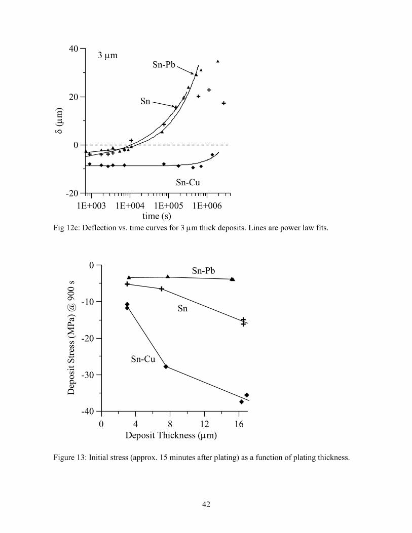
Fig. 13 shows a plot of the initial compressive stress (approx. 15 min after plating) versus
deposit thickness for the three deposit compositions using the parameter values in Table 2.
All stresses are compressive. For each alloy, the initial stress becomes more compressive with
increasing thickness. Because the diffusion fields in the electrolyte, and thereby the deposit
alloy compositions, reach steady state within the first 0.1 µm of deposition due to the rotation
of the electrode, the observed stress-thickness relationship cannot be attributed to a
concentration gradient in the deposition direction. The reason for the increase in the
magnitude of the compressive stress with deposit thickness is unclear.
Regardless of deposit thickness, the Sn-Cu deposits have the highest compressive stress, the
pure Sn has intermediate compressive stress, and the Sn-Pb deposit has the lowest
compressive stress. A positive correlation exists between the magnitude of the compressive
stress and the degree of disruption of the surface morphology; viz., the Sn-Cu samples have
whiskers and large contorted hillocks, the pure Sn has only small hillocks and the Sn-Pb
alloys are free of hillocks and whiskers.
4.4.2 Deflection vs. Time
14

As shown in Fig. 12, the beams return toward their initial positions with many of the samples
actually passing through the initial position. Use of Eqn. [14] would imply that the deposit
stress begins compressive and becomes tensile with time. However this is not necessarily
correct. To determine the average stress and the strain rate in the Sn and Sn alloy deposits
from the deflection data, we need to perform a “two layer Stoney analysis,” one layer for the
deposit and one for the growing IMC. The details of a model are given in the Appendix and
the analysis of the time dependence will be deferred to the discussion.
5 Discussion
5.1 Molar volume of Sn-Cu and Sn-Pb alloys
Before we can analyze the reasons for the various states of stress in the deposit, it is necessary
to consider the molar volume (volume per mole of atoms) for Sn-Cu and Sn-Pb alloys as
summarized by Figs. 14. For Sn-Cu, crystallographic data was used for the pure elements and
the Cu–rich phases. For Cu6Sn5, Fields et al. [27] measured a density of 8.28 g/cm3 that
converts to 10.6 cm3/mol1 (of atoms) using the composition of 0.44 atomic fraction Sn given
by [28]. In the same manner, the measured density of Cu3Sn, 8.90 g/cm3, converts to 8.6 cm3/
mole. The equilibrium solubility of Cu in solid Sn is very small: 6 x 10⁻³ mass fraction Cu at
227 °C [29] and 10-7 mass fraction Cu at room temperature (thermodynamic calculation [30]).
As noted above, however there is evidence from Fig. 10 that a supersaturated solid solution of
Cu in Sn is formed by the electrodeposition process. Because no lattice parameter data was
reported in [23], we require an estimate of the molar volume of Sn supersaturated with Cu,
1 The measured density agrees with the measured lattice parameters of the B82 (P63/mmc) structure of Cu6Sn5 if one considers the vacant 2d Wycoff sites required to achieve the correct phase composition.
15

Sn(Cu). Given the work on fast diffusion2 of Cu in Sn and the presumption that the Cu is
dissolved interstitially in Sn [31, 32] and in addition assuming that the partial molar volume
of interstitial Cu is zero, the volume per mole of atoms of supersaturated Sn(Cu) is shown in
Fig. 14 and is given by
( ) 16.28(1 )Sn CuM Cu= −V X [5]
where XCu it the mole fraction of Cu. These considerations would imply that the lattice
parameter of Sn is unchanged by the interstitial Cu. The lattice parameters for the Sn-Pb
system are summarized by [33]. Specifically, Sn rich Sn(Pb) solid solution up to 0.012 mass
fraction Pb were measured at 183 °C by [34]. After conversion from kX units to SI units and
changing the value of the intercept to get the accepted value for pure Sn at room temperature,
the results are
V [6] PbPbSn
M X52.328.16)( +=
where XPb it the mole fraction of Pb. This expression is plotted in Fig. 14.
We extract a few numbers from Fig. 14 for use below. First, the formation of a layer of
Cu6Sn5 at an interface between Sn and Cu is considered. The volumetric strain for this
process can be read directly from the graph or determined analytically. It is the difference
between the molar volume of the Cu6Sn5 and the molar volume of an unalloyed mixture of
pure Cu and pure Sn of the same average composition as the intermetallic. The fractional
change is -0.056. In other words, the IMC takes up 5.6% less volume than a rule of mixture
combination of the Sn and Cu reactants from which the IMC forms.
2 We note that Ni also exhibits fast diffusion in Sn [34] due to its interstitial nature and would be expected to exhibit the same molar volume behavior.
16

From Fig. 14 we can also extract the volume change when precipitation of Cu6Sn5 occurs
from a supersaturated Sn(Cu) solid solution of mass fraction 3 % Cu. It is the difference
between the molar volume of the supersaturated solution and the volume of a equilibrium
mixture of Sn and Cu6Sn5 of the same average composition as the supersaturated solution.
For a deposit of 3 % mass fraction Cu (5.5 % atom fraction), the fractional change in volume
is +0.022. That is, the volume of a supersaturated solution of Sn(Cu) expands by 2.2 % when
it transforms to an equilibrium mixture of Sn and Cu6Sn5 phases. Finally, the volume change
of material that undergoes precipitation of Pb from a supersaturated Sn(Pb) solution can be
obtained from the graph. For a deposit of 2 % mass fraction Pb (1.16 % atom fraction), the
fractional change in volume is -0.0013. That is, the volume of a supersaturated solution of
Sn(Pb) shrinks by 0.13 % when it transforms to an equilibrium mixture of Sn and Pb phases.
5.2 Initial Stress
Understanding the causes of growth stress in thin films formed by electrodeposition (and by
other methods such as condensation from the vapor [36]) are active areas of research. We
consider here only the difference between the stress in the pure Sn, and those in the alloy
deposits. For a given thickness, we assume that the alloy deposits are formed with the same
growth stress as pure Sn and that the precipitation process in the alloys shortly after
deposition attempts to alter the deposit volume and hence change the stress prior to the first
measurement. Table 3 gives the experimentally determined deviation of the stress-free strain
values above or below that determined for the pure Sn. Also given is 1/3 of the change in the
deposit volumetric strain expected from the change in molar volumes for precipitation from
supersaturated solid solutions described in Section 5.1.
Table 3: Effect of Alloying Addition on Initial Stress of 16 µm deposits
17

Deposit Material
Measured initial stress (MPa)
Corresponding stress-free strain
Deviation of stress-free strain from that for pure Sn
1/3 of volume change due to ppt. of Cu6Sn5 or Pb from Cu or Pb supersaturated Sn
Sn -15.5 2.3 x 10⁻⁴ --- ---
Sn-2%Pb -4.0 0.6 x 10⁻⁴ -1.7 x 10⁻⁴ - 4 x 10⁻⁴
Sn-3%Cu -36.5 5.6 x 10⁻⁴ 3.3 x 10⁻⁴ 7 x 10⁻³
Note from the Appendix that 02
43
f fTf f S
f f
dE L Eσ σδε ε= − = − −
If the model worked perfectly, the numbers in each row of the last two columns should be the
same. Similar results are obtained for the 3 µm and 7 µm thick electrodeposits, except the
experimental increments get smaller as the thickness decreases. This explanation produces the
correct trends for the alloys if not the correct numerical values; viz., that the addition of Cu
increases that state of compression over pure Sn and that Pb causes the stress to become less
compressive. The quantitative errors may be due to the difficulties in measuring the deposit
concentrations and/or the assumption that interstitial Cu has zero partial molar volume. A
positive value would decrease the proposed amount of expansion due to Cu6Sn5 precipitation
listed in the last column of Table 3 and improve the agreement.
5.3 Time dependence of beam deflection - Average creep response
With time the precipitates coarsen, a process assumed to not alter the deposit stress. To
account for the stress induced in the deposit due to the IMC formation on the interface
between the deposit and the substrate requires the use of the model and equations in the
Appendix. This analysis necessitates the choice of a value for the stress in the IMC layer, IMCσ
(more properly the stress free strain, 0IMCε ). The most negative choice for the intermetallic
stress free strain is obtained using 1/3 the value of the volumetric strain for planar IMC
18

formation from pure Sn and Cu; viz., 0IMCε =-0.02 (see section 5.1). Using the modulus for the
IMC in Table 2, IMCσ ≈ +4.8 GPa. This stress value is an upper bound because the IMC may
not swell isotropically during growth; e.g., it might expand more in the growth direction to
reduce the strain energy. A second estimate is obtained experimentally from in situ wafer
curvature measurements after the deposition of 100 nm of Sn onto a Cu coated glass
cantilever [16]. After 20 nm of IMC has formed, a beam deflection consistent with a tensile
stress in the IMC of +1.2 GPa was obtained. A more appropriate estimate for thicker IMC
layers comes from the following experiments. For three pure Sn cantilever electrodeposits, 16
µm thick and aged for approximately 3 x 10⁷ s, the Sn was removed by dissolution in
concentrated HCl. This procedure leaves the approximately 2.5 µm thick IMC behind. The
deflections of the beams (compared to the original unplated position) were then +7 µm, +30
µm and +37 µm; i.e., toward the deposit side. From these experiments we conclude that IMCσ
is between +11 MPa and +62 MPa ( 0IMCε = -10-4 and -5 x10⁻⁴). Lee and Lee [11] performed
similar stripping experiments but unfortunately did not report the IMC stress. Due to the
uncertainty in the proper value of 0IMCε , we will compute the stress in the electrodeposit using
the deflection data and several assumed values of 0IMCε .
fσ
0IMε
d 0ε
Using the measured deflections and the model and equations in the Appendix, we plot in Fig.
15 the deposit stress, , as a function of time for the 7 µm thick pure Sn deposit for several
values of 0IMCε . With C =0, the deposit stress changes sign from compression to tension at
the same time that the beam deflection changes sign; the deflection is proportional
to f f IMd C IMσ σ+ , (Eqns. A1 & A3). For a value IMC =-3 x 10⁻³, the stress remains C
19
compressive for all time despite the fact that the deflection changes sign. Thus the idea
presented by several authors that IMC formation on the interface between the substrate and
the deposit compresses the remaining Sn is confirmed. Fig. 16 shows the different parts of the
deposit strain for two of the case shown in Fig. 15. The total deposit strain, Tfε , is proportional
to the deflection (Eqns. A1 & A4) and is positive if the deflection is negative. The relative
sizes of the elastic and plastic parts derived from the model, elfε and pl
fε , depend on the
assumed value of 0IMCε . The elastic strain is always proportional to the stress.
0IMC
The plastic strain rate is determined by differentiation of the plastic strain and a plot of log (-
strain rate) vs. log (-stress) can be constructed. Such plots constitute the experimentally
obtained average compression creep response of the deposits if we can assume that steady
state creep behavior applies at each instant. Reassuringly, use of a positive value of 0IMCε (all
measurements and estimates yield negative values) leads to unrealistic plastic response; the
sign of the stress and strain rate are not the same. Extremely negative values of 0IMCε (e.g.
-2x10⁻²) lead to equally unphysical creep curves where the stress exponent increases with
decreasing compressive stress. These considerations place bounds on the value of 0IMCε .
The creep curves for the 16 µm thick deposits are shown in Fig. 17 for three values of 0IMCε , 0,
-0.001, -0.002 that span the full range of reasonable values for the 16 µm deposits. This
corresponds to IMC stress between +0 MPa and +244 MPa. One slides down the creep curve
as time progresses. For large compressive stress (early times, thin IMC), the curves are
independent of ε and exhibit stress exponents of approximately 3, 6, and 15 for the Sn-Pb,
20

Sn and Sn-Cu respectively. We also note that Sn-Pb creeps faster than pure Sn, which in turn
creeps faster than Sn-Cu. For smaller values of compressive stress (later time, thicker IMC),
the creep curves show considerable dependence on 0IMCε . The curves can be used to show just
how much the deposit compression is increased the intermetallic by drawing a horizontal line.
Overall this analysis suggests that IMC formation on the Cu/Sn interface does not greatly
increase the compressive stress over the level due to the initial plating stress in these
experiments.
5.4 Localized creep as a mechanism for whisker / hillock formation.
We presume that the creep curve for Sn-Pb shown in Fig. 17 represents uniform creep alone
because no whiskers, cones or hillocks form. The electrodeposit would swell slightly and
uniformly in thickness as the compressive stress relaxes. For incompressible plasticity, the
plastic strain (strain rate) normal to the electrodeposit surface equals minus two times the in-
plane strain (strain rate). On the other hand, the creep curves for Sn and Sn-Cu include the
nonuniform creep that produces the surface disruption. In other words the hillock and whisker
formation is part (or all) of the compression creep response of these materials when
constrained by a substrate. We note that the creep rates of the pure Sn and Sn-Pb deposits are
much slower than those reported for bulk samples of similar compositions with the same grain
size [37, 37].
As mentioned in the introduction, diffusional creep has been employed to explain hillock
growth in thin films. Following this approach, Tu [10] and Hutchinson et al. [39] have
proposed models for whisker growth velocity based on an imposed constant in-plane
compressive stress and grain boundary diffusion of Sn to the whisker base. Grain boundary
21

diffusion is expected to be the dominant self diffusion mechanism in Sn because the
holomogous temperature for Sn corresponding to room temperature is 0.6. With whiskers a
distance 2b apart and with diameter 2a, both models arrive at a tip growth velocity v given by
( )2
2v
ln /gb
f
DRTa b a
σ Ω
= −
[7]
where is the molar volume of Sn, Ω gbD a grain boundary diffusion coefficient, RT is the
Boltzmann factor and a signed stress, fσ , has been used. A stress gradient in the deposit with
cylindrical symmetry under each whisker is assumed to drive the flux of Sn toward that
whisker. The length differs in the two models significantly depending on the geometrical
details. The model of Hutchinson et al., which uses fd= , the deposit thickness, and
replaces gbD with 2gbD
gλ where λ and are the effective thickness of a grain boundary and
the grain size respectively, leads to the correct order of magnitude of whisker growth rate
using literature accepted values of the Sn grain boundary diffusion coefficient [40]. From
these models, one can compute the plastic strain rate normal to the deposit if it were averaged
over the entire deposit surface as
g
2 2v / fa b
2
d ; giving an in-plane creep rate for an
incompressible deposit of 2-v / 2 fa b d or
2 ln
gbf f
f
Dbd RTba
ε σΩ
=
[8]
We note that this prediction is linear in stress and would produce a creep rate with slope of
unity as superimposed in Fig. 17, where we have used fd= , gbDλ = 6 x 10-22 m3/s [40], g
=3 µm, Ω = 1.7 x 10⁻⁵ m3/mol, a= 2 µm and b=100 µm.
22
It is interesting to note, despite the approximations of this whisker growth model, that the
average strain rate derived from this model is roughly tangent to the creep curves for the pure
Sn, lies below the creep curves for Sn-Pb and cuts through the creep curve for Sn-Cu. As a
mechanism of creep, whisker growth would then be least active for Sn-Pb, be marginal for
pure Sn and occur readily for Sn-Cu. For Sn-Cu, creep likely occurs by a mechanism with
high exponent before whisker creep becomes dominant at lower compressive stress. This may
be related to the observation that whisker formation appears to have an “incubation time.”
The above calculation for whisker growth rate needs improvement. A detailed model is
beyond the scope of the present paper, but it would be a special case of Coble creep [41]. The
diffusion potential (chemical potential of Sn atoms minus chemical potential of vacancies) is
highest for grain faces with the most compressive normal stress. This would correspond to
grain faces with normals lying in the plane of the deposit due to the bi-axial in-plane stress
state; i.e., the columnar grain faces. Oblique grain faces would have lower diffusion potential
and grain faces parallel to the deposit surface would be least. (The surface of the deposit
would also have the least diffusion potential, but we presume surface diffusion is suppressed
by native oxide.) This difference in diffusion potential causes a flux of Sn along the normal
grain faces to oblique faces. If many oblique or parallel faces are located within the deposit
(as with the Sn-Pb deposits), creep is relatively uniform and no hillocks/whiskers would
occur. Averaged over many grains this uniform creep process leads to a slight thickening of
the deposit and a reduction in the in-plane stress without whisker formation.
If oblique or parallel faces occur rarely, as in the columnar structures of the Sn and Sn-Cu
samples, the diffusion flux is forced toward the free surface. Any oblique grain face near, but
23

under, the deposit surface would be ripe for accumulation of Sn and pushing of the grain
upward to produce surface features, such as hillocks and whiskers. As with any diffusional
creep process, grain boundary sliding and accommodation must occur simultaneously [42].
We note however that Sheng et al. [22] observe whisker growth from matte Sn and Sn-Cu
deposits even though the grain structure is not columnar. Thus avoiding columnar grain
structures should be considered only part of a general whisker mitigation strategy.
A proper model for whisker growth from a columnar grain structure must assess the grain
boundary diffusion path through a three dimensional network of columnar grain faces
connecting to oblique grain faces near the deposit surface, for example at a small surface
grain as shown in Fig. 18. Whisker growth would only be possible at a few small surface
grains formed at the end of the deposition process or possibly by recrystallization after
plating. Fig. 19 shows different situations for the response of a small surface grain depending
on the general grain shape and mobility of the grain boundaries in the electrodeposits. Fig
19a shows the case for pure Sn deposits with a columnar grain structure in which the active
surface grain can broaden laterally by grain boundary migration as it is pushed upward. The
localized creep is thus spread over a larger surface area; never forming a filamentary whisker.
In a film under stress, the seeds of a model for this lateral grain boundary motion and surface
upheaval on the trailing side can be found in [43]. Many hillocks appear to have a small flat
top at their center indicating the original location of the hillock grain prior to the migration of
its boundaries. For very thin deposits, hillock base broadening may be halted when the hillock
grain bottom has impinged on the layer IMC. If sufficient compressive stress remains, the
hillock may then grow in a more whisker-like manner. Such a process may be important for
deposits with thickness the same as the lateral grain size.
24

In Fig. 19b is depicted the situation for the Sn-Cu deposits where the grain boundaries are
pinned or impeded by IMC particles. These particles are formed by precipitation from Sn
supersaturated solid solution; i.e., where the Cu has come from the electrolyte. Hillock grain
base broadening is hindered and the upward motion of material is concentrated into contorted
hillocks or whiskers. Contorted hillocks occur when several surface grains with oblique
internal faces in close proximity are present; hence the multi-grained nature seen in Fig. 6.
Whiskers occur when a single surface grain with immobile oblique internal faces persists in
time for the Sn flux to continually accrete. Fig. 19c shows the case of the non-columnar
structure of Sn-Pb were many internal grain boundaries are available for accretion of Sn
producing a more uniform thickening of the deposit to relieve compressive stress.
6. Conclusions
1) Plating on cantilever beam samples, shows that compressive stresses are present in high
purity bright Sn electrodeposits within 15 minutes after plating. Intermetallic growth along the
Sn/Cu interface should be insignificant (6 nm thickness) over this short time at room
temperature. Thus compressive stresses are intrinsic to the plating process under the
conditions of our experiments.
2) Co-deposition of Sn with Cu or Sn with Pb in the amount of a few mass percent alters the
compressive stress compared to pure Sn by the time of first measurement. Larger
compressive stress is generated in the electrodeposit with Cu addition to the electrolyte;
smaller compressive stress is generated in the deposit with Pb addition to the electrolyte. The
increase/decrease in compressive stress for the alloys is due to volume changes of the deposit
caused by the solid state precipitation of Cu6Sn5 / Pb particles by metallurgical precipitation
from the supersaturated Sn-Cu / Sn-Pb solid solution formed by the plating process.
25

3) Cu addition does not alter the columnar grain structure found in pure Sn deposits, whereas
the Pb addition causes an equi-axed grain structure to develop.
4) The analysis of the time dependence of the measured beam deflections indicates that the
additional compressive stress due to intermetallic formation on the deposit / beam interface
over long time periods is of the same order of magnitude as the plating stress. It is not the sole
source of compressive stress.
5) Whiskers and contorted hillocks are observed on the Sn-Cu deposit surfaces, conical
hillocks are observed on the pure Sn deposits and no surface disturbances are found on the
Sn-Pb deposits.
6) We propose that the compressive stress in the deposits relaxes by Coble creep (grain
boundary transport of Sn and vacancies). For the equiaxed structure of the Sn-Pb deposits,
transport between interior grain faces with different normal stress permits uniform swelling of
the deposit thickness and no localized surface disturbance. For the columnar structures of the
Sn and Sn-Cu deposits, the Sn flows toward the free surface. In the absence of surface
transport due to native oxide, the Sn accumulation is localized to oblique grain faces near but
under the free surface that forces the grain upward.
7) The lack of lateral grain boundary mobility of the columnar structure in the Sn-Cu deposits
caused by precipitate pinning is thought to promote whisker formation by maintaining a
laterally small grain where Sn flux accumulates. Rather benign (electronically) hillock
formation occurs in pure Sn due to extensive lateral grain boundary migration.
8) A suggested whisker mitigation strategy based on this work would be to avoid impurities in
the electrolyte such as Cu that are fast diffusers and hence occupy interstitial sites in the Sn
lattice. Electrolytes containing solutes occupying substitutional sites in the Sn lattice and also
26

whose precipitation from supersaturated solid solution tends to reduce the volume of the
deposit should be beneficial.
9) A second suggestion is to employ plating conditions and/or additives to the electrolyte that
break up the columnar structure and promote the formation of grain boundaries parallel to the
deposit surface. Such boundaries would allow a more uniform creep of electrodeposits to
relieve compressive stress.
Acknowledgements
The authors are indebted to R. Parke and S. Claggett for the TEM sample preparation, to R.
Fields for the phosphor bronze mechanical measurements, U. R. Kattner for thermodynamic
calculations and to Daniel Josell for many fruitful discussions regarding beam deflection.
Thanks are also in order to G. Galyon and M. Palmer for the FIB pictures, which greatly
clarified the microstructures and assisted this research.
Appendix: Time dependent deflection of a beam with two thin films
To estimate the stresses in each layer, which can not be individually determined from the beam deflection, we develop a model to describe the time dependent deflection of the beam. The deflection is due to three causes: 1) an initial residual stress in the deposit due to plating and fast precipitation processes, that is assumed independent of time, 2) stress due to the growth of a layer of IMC that forms between the Sn and Cu substrate that has a different volume than the Sn and Cu from which it formed; (3) relaxation due to creep. The model assumes that the creep is uniform. For this model, we will employ the thin deposit approximation, to avoid unnecessary complication in the exposition. Let iσ , d ,i iε be the stress, thickness, strain and modulus in layer i where i =IMC or f for the planar IMC layer and electrodeposited film respectively. Let the beam curvature be given by
iE
2
)(2)(
1)(L
ttr
tK δ== [A1]
where ( ) 0tδ > if the electrodeposit surface is concave (deposit on top, curved up). To treat
the fact that the IMC layer thickens with time and the Sn layer thins with time, we use
27
0
0
( )
( )
(1 )
IMC
f f IMC
S S IM
d t Bt
d d sd t
d d s d
=
= −
= − − C
d
[A2]
where s ≈ 5/11. For , balance of moments and forces for the substrate and the two layers yields
and IMC f Sd d <<
( )'
2( ) ( ) ( ) ( ) ( ) ( )6
SIMC IMC f f S
Et d t t d t d t K tσ σ+ = . [A3]
With the thin approximation, the total strain in both layers (measured from a flat beam) is the same and is given by
2 ( ) ( )3
T TIMC f Sd t K tε ε= = − [A4]
The total strain in the IMC layer will be assumed to be the sum the stress-free strain due to its volume change from the reactants and its stress dependent elastic strain (no creep) 0T
IMC IMC IMCelε ε ε= + [A5]
with 0el T
IMC IMC IMC IMC IMC IMCE Eσ ε ε ε′ ′ = = − . [A6] The total strain in the Sn deposit will be assumed to be the sum of the stress free strain due to the electrodeposition process (plus the fast precipitation processes in the alloys), stress dependent elastic and plastic strains 0T el pl
f f f fε ε ε ε= + + [A7] with 0el T pl
f f f f f f fE Eσ ε ε ε′ ′ ε = = − − [A8] and (pl )f ffε σ= [A9] where the dot denotes a time derivative. The function ( )ff σ could represent power law creep for example of the form pl n
f fKε σ= . [A10]
For choices of a parabolic growth constant B, and a value for 0IMCε , one can extract
or its time derivative from the measured data, 0f( ) and the quantity ( )pl
f ft tσ +( )t
ε ε ( )tplfε
δ . On can then plot log strain rate vs. log stress for the electrodeposit to estimate the function, Eqn. [A9]. Because the stress and strain rates are negative (compression creep), absolute values are used for Fig. 17. Alternately, one can convert these equations to a system of coupled ordinary differential equations for ( )tδ , ( )f tσ , ( )IMC tσ and for a given creep law and the other materials parameters. Numerical solution shows how the electrodeposit stress is affected by the growing IMC. In general the stress in the film becomes slightly more compressive due to the IMC growth. The amount is sensitive to the how positive is the chosen value of
( )plf tε
0IMCε .
28

References 1. Furuta N, Hamamura K. Jap. J. Appl. Phys 1969; 8:1404. 2. Kabakian L, Chason E, Kumar KS, Spring MRS 2003. 3. Fisher RM, Darken LS, Carroll KG. Acta Met 1954; 2: 368. 4. Arnold SM. Plating, 1966; 53: 96. 5. Galyon GT, “Annotated Tin Whisker Bibliography,” National Electronics
Manufacturing Initiative Inc. (NEMI), Herdon VA, July 2003. (www.nemi.org) 6. Chadhari P. J. Appl. Phys 1974; 45: 4339. 7. Jackson MS, Li C-Y. Acta Met 1982; 30: 1993. 8. Doerner MF, Nix WD. CRC Critical Reviews in Solid State and Materials Sciences
1988; 14: 225. 9. Tu KN. Acta Met 1973; 21: 347. 10. Tu KN. Phys. Review B-Condensed Matter 1994; 49: 2030. 11. Lee BZ, Lee DN. Acta Mat 1998; 46: 3701. 12. Moon K-W, Williams ME, Johnson CE, Stafford GR, Handwerker CA, Boettinger WJ,
in “Proceedings of the Fourth Pacific Rim International Conference on Advanced Materials and Processing,” The Japanese Institute of Metals, Sendai, Japan, 2001, Hanada S, Zhong Z, Nam SW, Wright RN, eds., pp. 1115-1118.
13. Weil R. Plating 1971; 58: 137. 14. Onishi M, Fujibuchi H. Trans. J. Inst. Metals 1975; 16: 539. 15. Tu KN, Thompson RD. Acta Met 1982; 30: 947. 16. Stafford GR, Bertocci U, Guyer JE, NIST (2004) unpublished research. 17. Bard AJ, Faulkner LR. “Electrochemical Methods: Fundamentals and Applications,”
(New York: John Wiley and Sons, Ltd., 1980) pp. 288. 18. Galyon GT, Palmer M, IBM, 2004, unpublished images of NIST samples. 19. Petersson I, Ahlberg E. J. Electroanal. Chem. 2000; 485; 166. 20. Tindall GW, Bruckenstein S. Anal. Chem., 1968; 40: 1402. 21. Brenner A., “Electrodeposition of Alloys”. Vol.1. 1963, New York: Academic Press.
p.195. 22. Sheng GTT, Hu CF, Choi WJ, Tu KN, Bong YY, and Nguyen L, J. Appl. Phys. 2002;
92: 64. 23. Kane RH, Giessen BC, Grant NJ. Acta Met 1966; 14: 605. 24. Kim D-K, Nix WD, Deal MD, and Plummer JD. J. Mater. Res 2000; 15 :1709 25. Brenner A, Senderoff S. J. of Research of the NBS 1949; 42: 105 26. Metal Reference Book, Smithells CJ, 4th edition, Plenum Press, NY 1967. 27. Fields RJ, Low III SR, , Lucey, Jr. GK. in “Metal Science of Joining,” Cieslak MJ,
Perepezko JH, Kang S, Glicksman, ME, eds., The Minerals, Metals & Materials Society, Warrendale, PA., pp. 165-173, 1992.
28. Saunders N, Miodownik AP. Bull. of Alloy Phase Diagrams 1990; 11: 278 29. Homer CE, Plummer H. J. Inst. Metals 1939; 64:169. 30. Kattner UR, NIST , Gaithersburg, MD, 2002, unpublished research. 31. Dyson BF, Anthony TR, Turnbull D. J. Appl. Physics 1967; 38: 3408. 32. Warburton WK, Turnbull D. Thin Solid Films 1975; 25: 71 33. Karakaya I, Thompson WT. Bull. of Alloy Phase Diagrams 1988; 9: 144. 34. Lee JA, Raynor GV. Proc. Phys. Soc. 1954; 67: 737. 35. Yeh DC, Huntington HB. Phys. Rev. Lett 1984; 53: 1469. 36. Floro JA, Chason E, Cammarata RC, Srolovitz D, MRS Bulletin 2002; 27:19.
29

37. Schneibel JH, Hazeldine PM. J. Matl. Sci 1983; 18: 562. 38. McCabe RJ and Fine ME, Metall.& Mater. Trans. 2002: 33A:1531. 39. Hutchinson B, Oliver J, Nylén M, Hagström J, Mat. Sci. For 2004; 467-470: 465. 40. Kaur I, Gust W. “Handbook of Grain Boundary and Interface Boundary Diffusion Data”, (Ziegler Press, Stuutgart 1989 Vol. 2, p. 1277. 41. Coble RL. J. Appl. Phys. 1963; 34: 1679. 42. Raj R, Ashby MF. Met. Trans. 1971; 2: 1113. 43. Genin FY, J. Appl. Phys. 1995; 77: 5130.
30

Fig. 1: Drawing of a cantilever beam coupon with plated region shown in gray. The three frame positions used for tip position measurement are indicated. Dimensions are in mm.
31
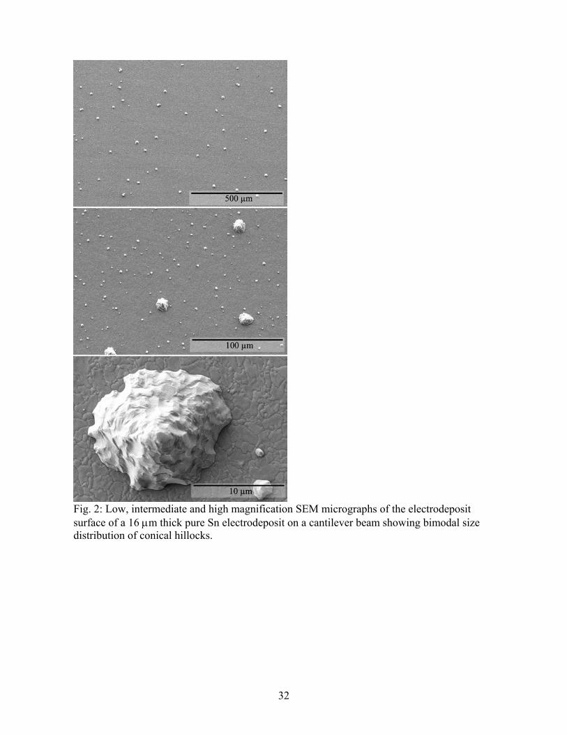
Fig. 2: Low, intermediate and high magnification SEM micrographs of the electrodeposit surface of a 16 µm thick pure Sn electrodeposit on a cantilever beam showing bimodal size distribution of conical hillocks.
32

Fig. 3: SEM image of FIBed sample showing small and large hillocks on a 16 µm thick pure Sn electrodeposit. IMC and the bronze are seen at the bottom [18]. The white contrast on the Sn columnar grain boundaries is an artifact of the FIB procedure as is the darker contrast in the hillock grain above the deposit surface.
33

Fig. 4: Low, intermediate and high magnification SEM micrographs of the electrodeposit surface of a 16 µm thick Sn-Cu electrodeposit on a cantilever beam (photo taken after 176 days (1.5 x10⁷ s)). The fine lines center and lower right in the top figure are long whiskers. A few Sn grain boundary locations are indicated in the bottom figure.
34

Fig. 5: Time sequence of the formation of an eruption on a Sn-Cu 16 µm thick cantilever sample. Prior to 2 days (1.5 x10⁵ s) no surface upheaval is observed.
35

Fig. 6: SEM images of FIBed 16 µm thick Sn-Cu electrodeposit. a) location showing a contorted eruption, .b): location showing a filamentary whisker on the same sample. [18].
36

Fig. 7: Low, medium and high magnification SEM micrographs of the electrodeposit surface of a 16 µm thick Sn-Pb electrodeposit on a cantilever beam after 85 days (7.3 x10⁶ s). The highest magnification SEM micrograph employed back scattered electron contrast and clearly shows four isolated Pb grains.
37

Fig. 8: SEM images of FIBed 16 µm thick Sn-Pb electrodeposit. The grain structure is not columnar. [18].
Fig. 9: Cross sections of 16 µm thick (nominal) electrodeposits on phospor bronze: a) Pure Sn, b) Sn-Cu, c) Sn- Pb approximately one year after plating.
38

Fig.10: TEM a) bright and b) dark field views of Sn-Cu deposit approximately 24 h after electroplating. Cu6Sn5 intermetallic particles were identified by SAD in the interior of the Sn grains and on the grain boundaries. The dark field images show that the internal particles share a common orientation.
39

Fig. 11: TEM of Sn Pb-electro deposit one month after plating: a) Pb particles are approximately 50 nm tetragonally distorted cuboids within the Sn grains and b) larger Pb particles on the Sn grain boundaries.
40

1E+003 1E+004 1E+005 1E+006time (s)
-160
-120
-80
-40
0
40δ
(µm
)16 µm
Sn
Sn-Pb
Sn-Cu
Fig 12a: Deflection vs. time for 16 µm thick deposits. Lines are power law fits.
1E+003 1E+004 1E+005 1E+006time (s)
-60
-40
-20
0
20
40
δ (µ
m)
Sn
Sn-Cu
Sn-Pb7 µm
Fig. 12b: Deflection vs. time curves for 7 µm thick deposits. Lines are power law fits.
41
1E+003 1E+004 1E+005 1E+006time (s)
-20
0
20
40δ
(µm
)3 µm
Sn-Cu
Sn
Sn-Pb
Fig 12c: Deflection vs. time curves for 3 µm thick deposits. Lines are power law fits.
0 4 8 12 1Deposit Thickness (µm)
6-40
-30
-20
-10
0
Dep
osit
Stre
ss (M
Pa) @
900
s
Sn
Sn-Pb
Sn-Cu
Figure 13: Initial stress (approx. 15 minutes after plating) as a function of plating thickness.
42

0 20 40 60 80 1at fraction (% Cu)
00
8
12
16V
M (c
m3 /m
ole
of a
tom
s)
Sn Cu
Cu6Sn5
Cu3Snαβγ
Sn(Cu)
rule of mixtures of Sn and Cu
two phase equilibrium mixtureof Sn and Cu6Sn5
0 20 40 60 80 1at fraction (% Pb)
0016
16.5
17
17.5
18
VM
(cm
3 /mol
e)
Sn Pb
two phase equilibrium mixture
Sn(Pb)
Pb(Sn)
Fig. 14: Volume per mole of atoms for phases for the Sn-Cu and Sn-Pb systems. Dashed lines show supersaturated solid solutions. The vertical arrows show the volume change for the various metallurgical processes.
1E+002 1E+004 1E+006
Time (s)
-10
-5
0
5
10
15
Dep
osit
Stre
ss (M
Pa)
ε0IMC
-3e-3-2e-3-1e-3
0
Fig. 15: Deposit stress vs. time extracted from deflection data for pure Sn, 7 µm thick samples. Curves are shown from top to bottom for four different values of the intermetallic stress-free strain, 0
IMCε : 0, -1 x 10⁻³, -2 x10⁻³, -3x10⁻³.
43

(a)
(b)
Fig. 16: Strain vs. time histories. The total deposit strain is proportional to the measured deflection. Elastic strain and stress free + plastic strain are extracted from deflection data using the model for two assumed values of intermetallic stress-free strain: (a) 0 and (b) -3x10-
3. Note that in (b) that the elastic strain, which is proportional to the stress, is compressive for all times even though the deflection changes sign.
44

Fig. 17: Log (-plastic strain rate) vs. Log (-stress) for 16 µm thick electrodeposits derived
from deflection measurements. For each material: Bottom curve, no correction for layer intermetallic stress; Center curve, corrected for layer intermetallic stress, e0
IMC= -0.001 (stress = 125 MPa tensile); Top curve, e0IMC= -0.002 (stress = 250 MPa
tensile). The prediction of [39] for whisker growth rate (converted to average strain rate in the in-plane direction) is shown dashed.
45
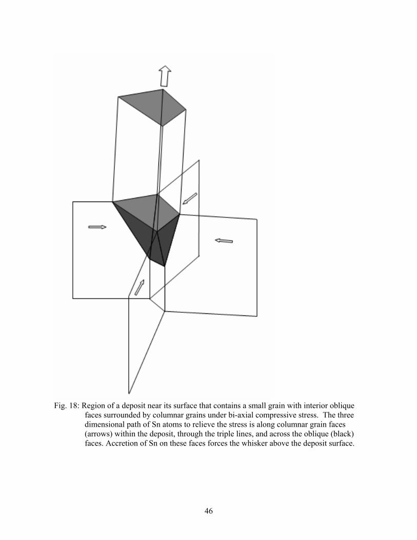
Fig. 18: Region of a deposit near its surface that contains a small grain with interior oblique
faces surrounded by columnar grains under bi-axial compressive stress. The three dimensional path of Sn atoms to relieve the stress is along columnar grain faces (arrows) within the deposit, through the triple lines, and across the oblique (black) faces. Accretion of Sn on these faces forces the whisker above the deposit surface.
46

Fig 19: Due to the absence of transverse grain boundaries in the columnar grain structures of (a) Sn or (b) Sn-Cu, in-plane compressive stress is relieved by hillock or whisker growth respectively depending on whether the grain boundaries are (a) mobile or (b) pinned. In the more equi-axed structure of Sn-Pb, uniform creep is possible and there is no need to from surface protrusions.
47