whyte, griogair w.m. (2008) antennas for wireless sensor
TRANSCRIPT

Glasgow Theses Service http://theses.gla.ac.uk/
Whyte, Griogair W.M. (2008) Antennas for wireless sensor network applications. PhD thesis. http://theses.gla.ac.uk/408/ Copyright and moral rights for this thesis are retained by the author A copy can be downloaded for personal non-commercial research or study, without prior permission or charge This thesis cannot be reproduced or quoted extensively from without first obtaining permission in writing from the Author The content must not be changed in any way or sold commercially in any format or medium without the formal permission of the Author When referring to this work, full bibliographic details including the author, title, awarding institution and date of the thesis must be given

1
Antennas for Wireless Sensor
Network Applications
by
Griogair W.M. Whyte
Department of Electrical and Electronic Engineering
Thesis submitted for the degree of
Doctor of Philosophy
to the
Department of Electronics and Electrical Engineering
Faculty of Engineering
University of Glasgow
© G. W. M. Whyte, 2008
2
Abstract
The objective of this thesis is to present an analysis of antennas, which are
applicable to wireless sensor networks and, in particular, to the requirements of
the Speckled Computing Network Consortium. This was done through a review of
the scientific literature on the subject, and the design, computer simulation, and
experimental verification, of various suitable designs of antenna
The first part of this thesis outlines what an antenna is and how it radiates. An
insight is also given to the fundamental limitations of antennas. As antennas
investigated in this thesis are planar-printed designs, an insight into the types of
feed lines applicable, such as microstrip, CPW and slotline, is given. To help
characterise the antennas investigated, the fundamental antenna analysis
parameters, such as impedance bandwidth, S-parameters, radiation pattern,
directivity, antenna efficiency, gain and polarisation are discussed. Also
discussed is the 3D electromagnetic simulation software, HFSS, which was used
to simulate the antennas in this thesis. To help illustrate the use of HFSS, a
proximity-coupled patch antenna, operating at 5.8 GHz, was used as an example.
A range of antennas were designed, manufactured and tested. These used
conventional printed circuit boards (PCBs) and Gallium Arsenide (GaAs)
substrates, operating at a range of frequencies from 2.4 GHz to 12 GHz.
A review was conducted into relevant, suitable radio architectures such as,
conventional narrowband systems, Ultra-Wide Band (UWB), and simplified radio
architectures such as those based on the diode rectifier method, and Super
Regenerative Receivers (SRR).
There were several UWB antennas designed, which operate over a 3.1 – 10.16
GHz operational band with a VSWR ≤ 2. All the UWB antennas were required to
transmit a UWB pulse with minimal distortion, which placed a requirement of
linear phase and low values of group delay to minimise distortion on the pulse.
UWB antennas investigated included a Vivaldi antenna, which was large,

3
directional and gave excellent pulse transmission characteristics. A CPW-fed
monopole was also investigated, which was small, omni-directional and had poor
pulse transmission characteristics.
A UWB dipole was designed for use in a UWB channel modelling experiment in
collaboration with Strathclyde University. The initial UWB dipole investigated
was a microstrip-fed structure that had unpredictable behaviour due to the feed,
which excited leakage current down the feed cable and, as a result, distorted both
the radiation pattern and the pulse. To minimise the leakage current, three other
UWB dipoles were investigated. These were a CPW-fed UWB dipole with slots,
a hybrid-feed UWB dipole, and a tapered-feed UWB dipole. Presented for these
UWB dipoles are S-parameter results, obtained using a vector network analyser,
and radiation pattern results obtained using an anechoic chamber.
There were several antennas investigated in this thesis directly related to the
Speckled Computing Consortiums objective of designing a 5mm3 ‘Speck’. These
antennas were conventional narrowband antenna designs operating at either 2.45
GHz or 5.8 GHz. A Rectaxial antenna was designed at 2.45 GHz, which had
excellent matching (S11 = -20dB) at the frequency of operation, and an omni-
directional radiation pattern with a maximum gain of 2.69 dBi as measured in a
far-field anechoic chamber. Attempts were made to increase the frequency of
operation but this proved unsuccessful.
Also investigated were antennas that were designed to be integrated with a 5.8
GHz MMIC transceiver. The first antenna investigated was a compact-folded
dipole, which provided an insight into miniaturisation of antennas and the effect
on antenna efficiency. The second antenna investigated was a ‘patch’ antenna.
The ‘patch’ antenna utilised the entire geometry of the transceiver as a radiation
mechanism and, as a result, had a much improved gain compared to the compact-
folded dipole antenna. As the entire transceiver was an antenna, an investigation
was carried into the amount of power flow through the transceiver with respect to
the input power.

4
“Gin a body meet a body
Flyin' through the air,
Gin a body hit a body,
Will it fly? and where?
Ilka impact has its measure,
Ne'er a ane hae I,
Yet a' the lads they measure me,
Or, at least, they try.
Gin a body hit a body
Altogether free;
How they travel afterwards
We do not always see.
Ilka problem has its method
By analytics high;
For me, I ken nae ane o’ them,
But what the waur am I?”
— James Clerk Maxwell Rigid Body Sings (l. 1–4)

5
Table of Contents
List of Figures ..........................................................................................................8
List of tables...........................................................................................................17
Acknowledgments..................................................................................................18
Authors declaration................................................................................................19
1. Introduction........................................................................................................20
2. An introduction to antennas ...............................................................................23
2.1 What is an antenna? ..................................................................................... 23 2.2 Types of antennas ........................................................................................ 26
2.2.1 Wire antennas......................................................................................... 26 2.2.2 Aperture antennas .................................................................................. 26 2.2.3 Array Antennas ...................................................................................... 26 2.2.4 Printed Antennas.................................................................................... 27
2.3 Radiation Mechanism .................................................................................. 27 2.4 The Dipole ................................................................................................... 29 2.5 Antenna Field Region .................................................................................. 32
2.5.1 Reactive near-field region......................................................................32 2.5.2 Radiating near-field or Fresnel region ................................................... 32 2.5.3 Radiating far-field or Fraunhofer region................................................ 33 2.5.4 Characteristic impedance of EM waves................................................. 33 2.5.5 Velocity of Propagation .........................................................................34
2.6 The fields of a short electric dipole.............................................................. 35 2.7 The fields of a finite length dipole............................................................... 45
3. Fundamental limitations of small antennas........................................................51
3.1 Wheeler limit ............................................................................................... 51 3.2 Chu-Harrington Limit .................................................................................. 52 3.3 Mclean Limit................................................................................................ 55 3.4 Fundamental Limits of a 5.8 GHz antenna .................................................. 56
4. Transmission lines .............................................................................................58
4.1 Basic transmission line theory ..................................................................... 58 4.2 Transmission Lines ...................................................................................... 59
4.2.1 Two-wire transmission line.................................................................... 59 4.2.2 Parallel plate waveguide ........................................................................60 4.2.3 Co-Axial line.......................................................................................... 60 4.2.4 Microstrip............................................................................................... 61 4.2.5 Co-Planar Waveguide (CPW)................................................................ 63 4.2.6 Slotline ................................................................................................... 64
5. Antenna Analysis ...............................................................................................67
5.1 Fundamental Antenna Parameters ............................................................... 67 5.1.1 Impedance Bandwidth ........................................................................... 67 5.1.2 S-Parameters .......................................................................................... 68 5.1.3 Radiation Pattern.................................................................................... 71 5.1.4 Directivity (D)........................................................................................ 72 5.1.5 Antenna Efficiency (η)........................................................................... 73 5.1.6 Antenna Gain ......................................................................................... 75

6
5.1.7 Polarisation ............................................................................................ 76 6. Antenna design, fabrication and experimental analysis.....................................79
6.1 High Frequency Simulation Software (HFSS) ............................................ 79 6.1.1 Theoretical basis of HFSS ..................................................................... 79 6.1.2 Simulating structures in HFSS............................................................... 81
6.3 Fabrication Processes................................................................................... 86 6.4 Testing facilities........................................................................................... 87
6.4.1 Near-field anechoic chamber ................................................................. 87 7. A proximity-coupled 5.8 GHz patch antenna ...................................................89
7.1 Background theory....................................................................................... 89 7.2 Design of Patch antenna - The transmission line model.............................. 91 7.3 Simulated Results......................................................................................... 94 7.4 Testing antenna and redesign....................................................................... 96
8. Ultra-Wide Band (UWB) Antennas.................................................................104
8.1 UWB Architecture ..................................................................................... 104 8.2 Key requirements for UWB antennas ........................................................ 105 8.3 Initial designs of UWB Antennas .............................................................. 107
8.3.1 UWB test system.................................................................................. 107 8.3.2 The Vivaldi Antenna............................................................................ 108 8.2.2 The CPW-fed Monopole Antenna ....................................................... 115
8.4 Initial UWB Evaluation ............................................................................. 121 9. A UWB channel modelling experiment..........................................................123
9.1 UWB test system........................................................................................ 123 9.2 UWB dipole ............................................................................................... 124
9.2.1 Microstrip Edge-fed UWB dipole........................................................ 125 9.2.1.1 Radiation pattern results ................................................................... 129 9.2.2 UWB dipole with slots......................................................................... 133 9.2.2.1 Effect of slots on antenna.................................................................. 133 9.2.2.2 S-parameter results for UWB dipole with slots ................................ 139 9.2.2.3 Radiation pattern results for UWB dipole with slots........................ 141 9.2.3 A hybrid feed for a edge-fed UWB dipole antenna ............................. 144 9.2.3.1 S-Parameter results for hybrid feed UWB dipole............................. 151 9.2.3.2 Radiation pattern results for hybrid feed UWB dipole ..................... 154 9.2.4 A tapered feed UWB dipole................................................................. 157 9.2.4.1 S-parameter results for tapered feed UWB dipole............................ 162 9.2.4.2 Radiation pattern results for tapered feed UWB dipole.................... 166
9.3 Comparison of UWB dipoles for pulse transmission ................................ 169 9.3.1 Pulse transmission via microstrip fed UWB dipoles ........................... 172 9.3.2 Pulse transmission via CPW-fed UWB dipole with slots.................... 174 9.3.3 Pulse transmission via hybrid feed UWB dipole................................. 176 9.3.4 Pulse transmission via tapered feed UWB dipole................................ 178
9.4 Evaluation of UWB dipoles....................................................................... 180 10. Narrowband Antenna Design.........................................................................181
10.1 Narrowband Radio Architectures ............................................................ 181 10.1.1 Diode rectifier .................................................................................... 181 10.1.2 Super Regenerative Receiver (SRR).................................................. 182 10.1.3 Comparison of SRR link budgets at varying frequencies.................. 183
10.2 The Rectaxial antenna.............................................................................. 186

7
10.2.1 Background theory............................................................................. 186 10.2.2 A 2.45 GHz rectaxial antenna............................................................ 189 10.2.3 Design of 5.8 GHz rectaxial antenna ................................................. 192 10.2.4 Surface waves in a grounded dielectric ............................................. 194 10.2.5 Field analysis of 5.8 GHz Rectaxial antenna..................................... 195
10.3 Integrated antennas at 5.8 GHz................................................................ 201 10.3.1 Quality factor, bandwidth and efficiency........................................... 202 10.3.2 A compact folded dipole antenna at 5.8 GHz.................................... 205 10.3.2.1 Balun design.................................................................................... 206 10.3.2.2 Design of compact-folded dipole antenna ...................................... 209 10.3.2.2.1 Width of dipole ............................................................................209 10.3.2.2.2 Printed dipole on substrate........................................................... 211 10.3.2.2.3 Slotline-fed dipole over a ground plane....................................... 213 10.3.2.2.4 Folded dipole over a ground plane with transceiver.................... 215 10.3.2.3 Final design of printed dipole folded around transceiver ............... 218 10.3.2.4 Simulated and experimental results for final design....................... 218
10.3.3 A ‘patch’ antenna at 5.8 GHz ............................................................... 221 10.3.4 A approximate gain measurement for integrated 5.8 GHz antennas .... 226
11. Discussion and conclusions ...........................................................................231
12. List of References ..........................................................................................235
12.1 Chapter 1.................................................................................................. 235 12.2 Chapter 2.................................................................................................. 235 12.3 Chapter 3.................................................................................................. 236 12.4 Chapter 4.................................................................................................. 236 12.5 Chapter 5.................................................................................................. 237 12.6 Chapter 6.................................................................................................. 238 12.7 Chapter 7.................................................................................................. 238 12.8 Chapter 8.................................................................................................. 238 12.9 Chapter 9.................................................................................................. 239 12.10 Chapter 10.............................................................................................. 240

8
List of Figures Figure 2.1 Antenna as a transition device…………………………………..........25
Figure 2.2 Transmission-line thevenin equivalent of antenna in transmitting
mode……………………………………………………………………………...25
Figure 2.3. Charge uniformly distributed in a circular cross section cylinder
wire........................................................................................................................27
Figure 2.4. Oscillating electric dipole consisting of two electric charges in simple
harmonic motion, showing propagation of an electric field and its detachment
(radiation) from the dipole. Arrows next to the dipole indicate current (I)
direction………………………………………………………………………….30
Figure 2.5. Electric field lines for a λ/2 antenna at (a) t = 0, (b) t = T/8, (c) t = T/4
and (d) t = 3T/8......................................................................................................31
Figure 2.6. Field regions of an antenna.................................................................32
Figure 2.7. A short dipole antenna........................................................................35
Figure 2.8. Electric field configuration.................................................................36
Figure 2.9. Geometry for a short dipole.................................................................36
Figure 2.10. Near- and far-field patterns of Eθ and Hφ..........................................44
Figure 2.11. Near-field pattern for Er component.................................................45
Figure 2.12 Approximate natural-current distribution for thin, linear, centre-fed
antennas of various lengths. ..................................................................................46
Figure 2.13. Finite dipole geometrical arrangement for a far-field
approximation........................................................................................................46
Figure 2.14. Polar plots for the radiation patterns of a dipole of length (a) 0.5λ (b)
0.75λ (c) 1λ (d) 1.25λ (e) 1.5λ (f) 1.75λ…………………………………………49
Figure 3.1 Sphere enclosing an electrically small radiating element…………….51
Figure 3.2. (a) Equivalent network of a vertically-polarised omni-directional
antenna (b) Equivalent circuit for N spherical modes……………………………53
Figure 3.3 Fundamental limit of Q versus antenna size………………………….57
Figure 4.1. Model of a section of transmission line……………………………..58
Figure 4.2 Parallel plate waveguide……………………………………………...60
Figure 4.3 Co-axial transmission line……………………………………………61

9
Figure 4.4 Conceptual evolution of a Microstrip line from a two-wire transmission
line. (a) To a two wire transmission line. (b) To a parallel-plate waveguide. (c) To
a microstrip line with no dielectric (d) To a microstrip line. ……………………62
Figure 4.5 (a) Coplanar Waveguide (CPW) geometry (b) Electric and magnetic
field distributions on CPW……………………………………………………….63
Figure 4.6 Slotline transmission line…………………………………………….64
Figure 4.7. Field distribution of slotline. Solid line is E-field and dashed line is
H-field. …………………………………………………………………………..65
Figure 5.1 An N-Port network…………………………………………………...69
Figure 5.2 Two port network definition………………………………………….70
Figure 5.3 Coordinate system for antenna analysis……………………………...72
Figure 5.4. Schematic diagram of antenna terminated in impedance ZT with plane
wave incident on antenna (a) and equivalent circuit (b) ………………………...74
Figure 5.5. Rotation of a plane electromagnetic wave and its polarisation ellipse at
z = 0 as a function of time. ………………………………………………………76
Figure 6.1. 3D structure sub divided into elements……………………………...81
Figure 6.2. 5.8 GHz proximity coupled patch antenna ………………………….81
Figure 6.3. Wave port excitation on a SMA connector………………………….82
Figure 6.4 HFSS model (a) with and (b) without radiation boundary…………...85
Figure 6.5 Solution data for seven passes………………………………………..85
Figure 6.6. Layout of chamber. R= probe to centre of AUT =111.5 cm……….88
Figure 7.1. Representative shapes of microstrip patch antennas………………..89
Figure 7.2. (a) Microstrip antenna (b) side view……………………………..…90
Figure 7.3. Physical and effective lengths of rectangular microstrip patch……...92
Figure 7.4. HFSS model of 5.8 GHz patch antenna with final dimensions……..95
Figure 7.5 Simulated results for (a) S11 and (b) 3D E-field……………………...96
Figure 7.6. Simulated (blue) and experimental (red) results for S11……………97
Figure 7.7. 5.8 GHz patch antenna with 10 cm SMA cable…………………….97
Figure 7.8. Surface current on 5.8 GHz patch antenna with 10 cm SMA cable...98
Figure 7.9. Simulated (blue) and experimental (red) results for S11…………….99
Figure 7.10 Geometrical layout of 5.8 GHz patch antenna with short circuit
stub……………………………………………………………………………….99
Figure 7.11. Effect of varying short circuit stub length on S11 The length is varied
from 8.5mm to 9.5mm.…………………………………………………………100

10
Figure 7.12. Simulated (blue), L=8.5mm, and experimental (red) results for
S11……………………………………………………………………………….100
Figure 7.13. Simulated results for 5.8 GHz antenna with short circuit stub..
(L=8.5mm) (a) Surface current (b) 3D E-field pattern…………………………101
Figure 7.14. Experimental radiation plots (a) horizontal cuts; red = principle cut;
blue = simulated (b) vertical cuts; red = principle cut; blue = simulated………102
Figure 8.1 Comparison of (a) Narrowband and (b) UWB architectures……….105
Figure 8.2 Basic block diagram of the test system……………………………..107
Figure8.3 (a) Output waveform from 4015C pulser with 10x attenuation (b)
Output waveform after the impulse forming network stage……………………108
Figure 8.4. (a) Schematic of Vivaldi antenna designed in this project schematic.
Length = 292.1mm, Width = 203.2 mm. (b) Magnified view of transition…….109
Figure 8.5. Plan view of Vivaldi Antenna showing the magnitude of the E-field
(V/m) …………………………………………………………………………...110
Figure 8.6. Simulated (blue) and experimental (red) S11 for Vivaldi antenna…110
Figure 8.7. Transmission response (S21) for Vivaldi. Distance between antennas
=20 cm..………………………………………………………………………...111
Figure 8.8. (a) Experimental group delay for Vivaldi antenna (b) magnified view
for group delay. Distance between antennas = 20 cm..………………………..112
Figure 8.9. Vivaldi simulated antenna 3D radiation (Gain (dB)) patterns for (a) 3
GHz (b) 6 GHz and (c) 9 GHz …………………………………………………114
Figure 8.10. Received pulse for Vivaldi antenna………………………………115
Figure 8.11. The CPW-fed monopole…………………………………………116
Figure 8.12. (a) Simulated (red) and (b) experimental (blue) S11 results for CPW-
fed monopole…………………………………………………………………...117
Figure 8.13. Transmission response (S21) for CPW-monopole. Distance between
antennas =20 cm..……………………………………………………………...118
Figure 8.14. Experimental (blue) results for Group delay Vs frequency……...119
Figure 8.15. Simulated radiation patterns for (a) 3 GHz (b) 6 GHz and (c) 9
GHz……………………………………………………………………………..120
Figure 8.16. Pulse received by CPW-fed monopole…………………………...121
Figure 9.1 Block diagram for Strathclyde UWB test system…………………...124
Figure 9.2. Elliptical dipole element with suggested feeding points (a) centre (b)
bottom and (c) edge. …………………………………………………………...124

11
Figure 9.3. Microstrip edge-fed UWB dipole with taper. The brown element is
the ‘GND’ for the microstrip feed.……………………………………………..126
Figure 9.4. Simulated (blue) and experimental (red) results for S11 Vs.
Frequency……………………………………………………………………….127
Figure 9.5. Microstrip-fed UWB dipole S11 phase results (і) simulated (blue) (іі)
experimental (red) ……………………………………………………………...128
Figure 9.6. Transmission response (S21) for Microstrip-fed UWB dipole.
Distance between antennas =20 cm. …………………………………………...128
Figure 9.7. Experimental group delay for microstrip edge-fed UWB dipole.
Distance between antennas = 20 cm. …………………………………………..129
Figure 9.8. Orientation of antenna with respect to coordinate system used for
measurements…………………………………………………………………...129
Figure 9.9. Microstrip edge-fed UWB dipole simulated 3D E-field radiation
patterns for (a) 3 GHz (b) 6 GHz and (c) 9 GHz……………………………….131
Figure 9.10 Microstrip-fed UWB dipole simulated (blue) and experimental (red)
horizontal and vertical cuts for (a) 3GHz (b) 6 GHz and (c) 9 GHz.…………..132
Figure 9.11. CPW-fed dipole with slots………………………………………...133
Figure 9.12. Current flow around the antenna at the cpw to co-axial interface...134
Figure 9.13. Comparison of CPW-fed dipole antenna (a) with and (b) without
slots……………………………………………………………………………..135
Figure 9.14 Analysis of leakage current using E-field vector plot……………..135
Figure 9.15. Simulated S11 results for the increasing slot length; blue = 6mm, red
= 8mm, green = 10mm, magenta = 12mm, black = 17mm…………………….136
Figure 9.16. (a) Real and (b) Imaginary input impedance versus frequency for
increasing slot length; blue = 6mm, red = 8mm, green = 10mm, magenta = 12mm,
black = 17mm…………………………………………………………………..137
Figure 9.17. (a) Vector surface current plots (a) 2.32 GHz and (b) 3 GHz
The slot = 17 mm for both plots. ………………………………………………138
Figure 9.18. Simulated (blue) and experimental (red) results for S11. …………139
Figure 9.19. UWB dipole with slots S11 phase results (і) simulated (blue) (іі)
experimental (red) ……………………………………………………………...140
Figure 9.20. Transmission response (S21) for CPW-fed UWB dipole with slots.
Distance between antennas =20 cm. …………………………………………...140

12
Figure 9.21. Experimental group delay for UWB dipole with slots. Distance
between antennas = 20 cm. …………………………………………………….141
Figure 9.22. Orientation of antenna with respect to coordinate system used for
measurements…………………………………………………………………...141
Figure 9.23. Simulated 3D E-field radiation patterns for (a) 3 GHz (b) 6 GHz and
(c) 9 GHz………………………………………………………………………..143
Figure 9.24 CPW-fed UWB dipole with slots simulated (blue) and experimental
(red) horizontal and vertical cuts for (a) 3GHz (b) 6 GHz and (c) 9 GHz……..144
Figure 9.25. Hybrid-feed UWB dipole………………………………………...145
Figure 9.26. HFSS model for parallel plate interaction with metal (a) GND clear
(b) signal clear…………………………………………………………………..146
Figure 9.27. S11 and S22 for sub thickness = 2.286 mm; Blue (S11) and Red (S22)
belong to signal clear (Figure 6.22 (b)); Green (S11) and Magenta (S22) belong to
GND clear (Figure 6.22 (a)). …………………………………………………...147
Figure 9.28 Insertion Loss for sub thickness = 2.286 mm – GND clear (blue),
Signal clear (red)………………………………………………………………..147
Figure 9.29. Balanced feed UWB dipole (a) top view (b) underside view (c) 3D
see-through view………………………………………………………………..149
Figure 9.30 Comparison of leakage current at 3 GHz on UWB dipole antennas
(a) CPW feed with slots (b) balanced feed……………………………………..150
Figure 9.31 Far-field pattern for hybrid feed UWB dipole connected to co-axial
cable…………………………………………………………………………….151
Figure 9.32. S11 for simulated (blue) and practical (red) ……………………...152
Figure 9.33 Simulated (blue) and experimental (red) results for phase………...152
Figure 9.34. Transmission response (S21) for hybrid fed UWB dipole. Distance
between antennas =20 cm..……………………………………………………..153
Figure 9.35. Experimental group delay for hybrid fed UWB dipole. Distance
between antennas = 20 cm..…………………………………………………….153
Figure 9.36. Orientation of antenna with respect to coordinate system used for
measurements…………………………………………………………………...154
Figure 9.37. Simulated 3D E-field radiation patterns for hybrid fed UWB dipole at
(a) 3 GHz (b) 6 GHz and (c) 9 GHz…………………………………………….155
Figure 9.38 Hybrid feed UWB dipole simulated (blue) and experimental (red)
horizontal and vertical cuts for (a) 3GHz (b) 6 GHz and (c) 9 GHz…………...156

13
Figure 9.39. Layout of microstrip to parallel-plate tapered line balun. Overall
dimensions - length = 71.6mm, width = 9.52mm………………………………157
Figure 9.40. Surface current plot for balun at 3 GHz………………………….158
Figure 9.41 Simulated S-parameter results for balun. S21 = Green; S11 = Blue; S22
= Red……………………………………………………………………………159
Figure 9.42 Geometrical layout of tapered feed UWB antenna. W = 30.875mm; L
= 38.35mm……………………………………………………………………...160
Figure 9.43 Analysis of surface current on tapered feed antenna connected to co-
axial cable………………………………………………………………………160
Figure 9.44. Comparison of 3D e-field patterns connected to a co-axial cable for
(a) Hybrid feed UWB dipole and (b) Tapered feed UWB dipole………………161
Figure 9.45. Tapered-feed UWB dipole S11 results for simulated (blue) and
experimental (red) ……………………………………………………………...162
Figure 9.46. E-field at 10.16 GHz for (a) Tapered feed UWB dipole (b) half-
wavelength dipole………………………………………………………………163
Figure 9.47. Simulated (blue) and experimental (red) results for phase……….164
Figure 9.48. Transmission response (S21) for tapered feed UWB dipole. Distance
between antennas =20 cm..……………………………………………………..165
Figure 9.49. Experimental group delay for tapered feed UWB dipole. Distance
between antennas = 20 cm..…………………………………………………….165
Figure 9.50. Orientation of antenna with respect to coordinate system used for
measurements…………………………………………………………………...166
Figure 9.51. Simulated 3D E-field radiation patterns for tapered feed UWB dipole
at (a) 3 GHz (b) 6 GHz and (c) 9 GHz…………………………………………167
Figure 9.52 Tapered feed UWB dipole simulated (blue) and experimental (red)
horizontal and vertical cuts for (a) 3GHz (b) 6 GHz and (c) 9 GHz…………...168
Figure 9.53. Comparison of theoretical (blue) and experimental (red) results for a
100 ps pulse…………………………………………………………………….169
Figure 9.54. 1st derivative of Gaussian function experimental (red) and theoretical
(blue) results…………………………………………………………………….170
Figure 9.55. 2nd derivative of Gaussian function……………………………….171
Figure 9.56. Pulse received using microstrip-fed UWB dipole with filter (red) and
without filter (blue) …………………………………………………………….172

14
Figure 9.57. Pulse received using CPW-fed UWB dipole with slots with filter
(red) and without filter (blue) ………………………………………………….174
Figure 9.58. Pulse received using hybrid feed UWB dipole with filter (red) and
without filter (blue) …………………………………………………………….176
Figure 9.59. Pulse received using tapered-feed UWB dipole with filter (red) and
without filter (blue) …………………………………………………………….178
Figure 10.1. Diode rectifier circuit…………………………………………….182
Figure 10.2. Block diagram of complete narrowband transceiver……………..182
Figure 10.3. Output voltage vs. Input power for diode rectifier and SRR……...183
Figure 10.4 Basic block diagram illustrating Friis equation……..……………..184
Figure 10.5. (a) Helix and associated dimensions (b) Relationship between
circumference, spacing, turn length, and pitch angle of a helix. ………………187
Figure 10.6. Dimensions and coordinates for (a) helix (b) loop and (c) dipole.
(d) Helix as a succession of loops and dipoles (e) Helix for normal mode
calculations……………………………………………………………………..188
Figure 10.7. Schematic of rectaxial antenna………………………………..….189
Figure 10.8. Diagram of rectaxial antenna with dimensions. …………...……..190
Figure 10.9 Return Loss (RL) results for both simulation (a) and measured (b)
results. …………………………………………………………………………191
Figure 10.10. Normalised radiation patterns obtained by both simulation and
measurement……………………………………………………………………192
Figure 10.11. Schematic of 5.8 GHz rectaxial antenna………………………...192
Figure 10.12. Return loss for 5.8 GHz rectaxial antenna……………………….193
Figure 10.13. (a) E-field for 2.45 GHz rectaxial antenna. (b) E-field for 5.8 GHz
rectaxial antenna………………………………………………………………..193
Figure 10.14. Comparison of surface currents on the ground planes. (a) 2.45 GHz
rectaxial antenna (b) 5.8 GHz rectaxial antenna………………………………..194
Figure 10.15. Geometry of a grounded dielectric slab………………………....194
Figure 10.16 E-field vector plot of substrate…………………………………...195
Figure 10.17 Vector surface current plot on the ground plane………………....196
Figure 10.18. Surface current plot (a) with and (b) without rectaxial
element………………………………………………………………………….197
Figure 10.19. Simulated plots for (a) 3D E-field (b) 3D Gain (dBi) (c) x-y cut of
E-field…………………………………………………………………………..198

15
Figure 10.20. (a) Rectaxial antenna with small ground plane (b) x-y cut of Electric
far-field radiation pattern……………………………………………………….199
Figure 10.21 x-y cuts for (a) 5.8 GHz rectaxial antenna and (b) pattern
multiplication of Figure 8.15 (c) and Figure 8.16 (b) ………………………….200
Figure 10.22. A 5.8 GHz MMIC Transceiver. Maximum dimensions, length =
6.2; width = 2.25 mm……………………………………………….…………..201
Figure 10.24. Folded dipole with transceiver attached……………………..….205
Figure 10.25. A CPW-to-slotline transition………………………………..…..206
Figure 10.26. Simulated results for S21(green), S11 (blue) and S22 (red). Stub
length=5mm…………………………………………………………………….207
Figure 10.27. Smith chart showing S11 at 5.8 GHz for increasing length of Slotline
termination……………………………………………………………………...208
Figure 10.28. Smith chart showing S11 at 5.8 GHz for CPW-to-slotline transition
for increasing length of stub……………………………………………………209
Figure 10.29. Half-wavelength dipole showing current distribution. Width =
0.4mm…………………………………………………………………………..210
Figure 10.30. Input resistance (Ω) with width variation of 50 µm (blue), 100µm
(red), 200µm (green), 300µm (magenta), 400µm (black) ……………………..210
Figure 10.31. Input reactance (Ω) with width variation of 50 µm (blue), 100µm
(red), 200µm (green), 300µm (magenta), 400µm (black) ……………………..211
Figure 10.32. Half-wavelength dipole placed on GaAs substrate…………..…212
Figure 10.33. Input resistance (Ω) with width variation of 50 µm (blue), 100µm
(red), 200µm (green), 300µm (magenta), 400µm (black) ……………………..212
Figure 10.34. Input reactance (Ω) with width variation of 50 µm (blue), 100µm
(red), 200µm (green), 300µm (magenta), 400µm (black) ……………………..213
Figure 10.35. Possible configuration of Speck (a) side view (b) plan view…...214
Figure 10.36. Slotline-fed dipole antenna over ground plane…………….…...214
Figure 10.37. Results for real (red) and imaginary (blue) input impedance for a
printed dipole antenna over a ground plane…………………………………….215
Figure 10.38. Layout for a slotline-fed folded dipole with the transceiver
body......................................................................................................................216
Figure 10.39. Results for real (red) and imaginary (blue) input impedance for a
printed dipole antenna over a ground plane…………………………………….216

16
Figure 10.40. Far-field gain (dB) plots for (a) Folded dipole over a ground plane
with transceiver (b) Slotline fed dipole over a ground plane…………………...217
Figure 10.41. Schematic of folded dipole over ground plane with CPW-slotline
transition………………………………………………………………………..218
Figure 10.42. Simulated (blue) and experimental (red) results for S11…….….219
Figure 10.43. Simulated input resistance (red) and reactance (blue).
Experimental input resistance (magenta) and reactance (green) ………….…...220
Figure 10.44. Simulated 3D Gain plot for folded dipole…………………….....220
Figure 10.45. Schematic of ‘patch’ antenna with main dimensions outlined….221
Figure 10.46. Vector plots for 5.8 GHz ‘patch’ antenna (a) E-field (b) Vector
surface current…………………………………………………………………..222
Figure 10.47. Simulated (blue) and experimental (green) S11 results for ‘patch’
antenna………………………………………………………………………….223
Figure 10.48. Simulated 3D gain plot for ‘patch’ antenna……………..………224
Figure 10.49. Transceiver body highlighted for Poynting vector calculation....225
Figure 10.50. Simulated surface loss density on 5.8 GHz transceiver body…...226
Figure 10.51. Experimental setup for gain measurement……………………...227
Figure 10.52. Experimental results for S21 for 5.8 GHz proximity-coupled patch
antenna with separations of 14.5cm (blue), 20cm (red), 25cm (green), 30cm
(magenta), and 40cm (black) …………………………………………………..228

17
List of tables
Table 8.1 Antenna performance table. CG = Constant Gain………………….122
Table 9.1. Performance comparison of UWB dipoles………………………....180
Table 10.1 Power link budget for 2.45 GHz……………………..……………185
Table 10.2 Power link budget for 5.8 GHz……………………………...…….185
Table 10.3 Power link budget for 5.8 GHz………………………………..…..185
Table 10.4 Calculated values for average gain at 5.5 GHz and 5.92 GHz…..…228
Table 10.5. Folded dipole - Signal received on spectrum analyser via patch
antenna for various separations with the calculated value of gain……………..229
Table 10.6. ‘Patch’ antenna - Signal received on spectrum analyser via patch
antenna for various separations with the calculated value of gain……………..229

18
Acknowledgments
I would like to thank all the staff and students at Glasgow University who have
helped me during my time and made it a very enjoyable stay.
In particular, I would like to thank my supervisor Prof. Iain Thayne for letting me
do the PhD in the first place. His door was always open and he was willing to
listen and give advice. I would also like to give a big thanks to Ian McGregor for
his help with a multitude of topics and the always enjoyable afternoon coffee
conversations with him. Special mentions to Khaled Elgaid and Edward Wasige
who were part of the Specknet group. Even though he has departed Glasgow, I
should give a special thanks to Harold Chong who I constantly harassed about
fabricating my designs in the clean room. Special thanks go to the rest of the
Ultrafast Systems group and the Speckled Computing Consortium, who I have
enjoyed working / socialising with.
I would also like to give a big thanks to the technical staff on level seven for their
help, in particular Stuart Fairbarn for his rapid fabrication of my antenna designs
and to Chris Hardy for the use of his desk and tools.
Thanks go to Faisal Darbai and Prof. Ian Glover of Strathclyde University for
letting me use their equipment whenever I wanted
Very special thanks go to my father, for his encouragement and advice on writing
reports, which helped me, not just throughout the course of this PhD, but my
entire academic career to date.
Lastly and by no means least I would like to give a very special thanks to my
girlfriend, Kirsty, as she has somehow managed to put up with me for very a long
time.
This thesis is dedicated to the memory of my grandfather James ‘Jimmy’
Marshall.

19
Authors declaration
I, Griogair Whyte, declare that the work contained within this thesis is solely
mine, except where acknowledged.

20
1. Introduction
Autonomous distributed wireless sensor networks such as those being
investigated by the Speckled Computing Consortium [1] are widely predicted to
have major growth opportunities in the coming years in numerous imaging,
safety, biomedical and environmental applications. In most of these areas, the
design challenges are somewhat different from contemporary wireless
communications systems in that data rates will be low, and power consumption
and size of the sensor node are the key issues.
Truly “plug and forget” functionality, and the opportunity to embed sensor nodes
into everyday objects or the surrounding environment, requires small volume
solutions, the majority of which will be occupied by a large enough battery to
prolong lifetime. These constraints place stringent requirements on the system for
the following reasons:
i. The communication frequency should be high enough in order to minimise the
size of antenna and thus sensor node, although operating at higher frequencies
incurs higher path loss, and higher DC power consumption due to higher losses
for the inter-node radio transceiver.
ii. Given the low RF power levels (due to DC power constraints), the transceiver
antenna should have as high a gain as possible, yet given the fact that the network
nodes are randomly deployed and can be moving with respect to one another, an
omni-directional radiation pattern is required.
iii. In addition to the constraint mentioned in (i) above, the total volume of the
antenna should be minimised to maximise the size of the battery.
iv. As large numbers of sensor nodes will be required in any network, all
component costs, including the antenna should be minimised.
There has been research into this topic by organisations other than Speckled
Computing Consortium, most notably Berkeley University and its Smart Dust
project [2]. The goal of the Smart Dust project is to build a self-contained,
millimetre-scale, sensing and communication platform for a distributed sensor
21
network. The device itself, called a ‘mote’, would be around the size of a grain of
sand and contain sensors, computational ability, bi-directional wireless
communications and a power supply, while being inexpensive enough to be
deployed by the hundreds. The science and engineering goal of the Speckled
Computing Consortium project is to build a complete, complex system into a tiny
volume using the newest technologies (as opposed to futuristic technologies),
which requires advances in integration, miniaturisation and energy management.
When the project started many applications were foreseen for this technology
such as:
• Weather/seismological monitoring on Mars
• Internet spacecraft monitoring
• Land / space communication networks
• Chemical / biological sensors
• Weapons stockpile monitoring
• Defence related sensor networks
• Inventory control
• Product quality monitoring
• Smart office spaces
• Sports
The main difference from Smart Dust is that the Speckled Computing Consortium
looks well beyond typical sensor networks applications. Smart Dust motes are
used in static networks, whereas specks are intended for use as dense,
decentralized networks in which the specks can be moved around, if required.
The other main difference is that Smart Dust uses a centralised controller. A good
analogy to describe Smart Dust would be a queen ant that directs the other ants.
Whereas, Specknet intends to be completely decentralised i.e. the ants thinking
for themselves; this gives a truly ubiquitous network. However, before the goal
of a truly ubiquitous network is realised there are many hurdles to overcome.
These are as follows:

22
• Synchronisation of the device is very important. If the Speck is meant to
be autonomous, when will it know to send or receive information?
• Power consumption. If the device is very small it can only have a limited
power supply and cannot remain ‘on’ at all times otherwise its lifetime
will be extremely short. It is therefore important for the project to come
up with the most energy efficient designs.
It was decided early in the project that there should be certain criteria which
each sub-section of the Speck should meet. The most important criteria, from
the RF front-end point of view, were;
• The Specks should be able to communicate 10cm apart
• Transmit-receive (Tx/Rx) while only consuming 400µW of power.
The initial work reported in this thesis focused on Ultra Wide-Band (UWB) due
to the perceived power savings, and the fact that it was a ‘new’ technology. UWB
is discussed from a radio architecture perspective but with the main focus being
on antenna design and performance.
Discussed in the following chapters is the development of a low power radio
architecture, which allowed for design of antennas at much higher frequencies
than originally anticipated. Antennas were investigated and designed for the
frequencies of 2.4 GHz and 5.8 GHz. Ultra-Wide Band (UWB) antennas were
investigated and designed. They operated over the frequency range of 3.1 to
10.16 GHz. Chapter 2 presents the history and theory of antennas. Chapter 3
evaluates common transmission lines used to feed antennas. Chapter 4 gives the
fundamental parameters used for evaluating antenna performance. Chapter 5
discusses the experimental procedure followed when designing and testing
antennas, such as the simulation software, fabrication procedure and the test
apparatus. The remaining chapters are concerned with the design, analysis and
testing of antennas fabricated.

23
2. An introduction to antennas
The history of antennas originates back to 1873 when James Clerk Maxwell
presented ‘A Treatise on Electricity and Magnetism’ [1]. This work drew from
empirical and theoretical work that had already been carried out by scientists such
as Gauss, Ampere, Faraday, and others. Maxwell took the theories of electricity
and magnetism and unified them. The equations he derived are presented below
in differential form.
Mt
BE
rr
r−
∂∂−=×∇ (2.1)
Jt
DH
rr
r+
∂∂=×∇ (2.2)
ρ=⋅∇ Dr
(2.3)
0=⋅∇ Br
(2.4)
Where, Er
is the electric field intensity (V/m).
Hr
is the magnetic field intensity (A/m).
Dr
is the electric flux density (C/m2).
Br
is the magnetic flux density (Wb/m2).
Mr
is the (fictitious) magnetic current density (V/m2).
Jr
is the electric current density (A/m2)
ρ is the electric charge density (C/m3)
Maxwell’s equations allow the calculation of the radiated fields from a known
charge or current distribution. They also give a description of the behaviour of
the fields around a known current distribution or a known geometry. Maxwell’s
equations can then be used to understand the fundamental principles of antennas.
2.1 What is an antenna?
The IEEE definition [2] of an antenna or aerial is:
‘a means for radiating or receiving radio waves’

24
Radio waves are also referred to as electromagnetic waves, or light waves, as they
travel at the speed of light and can be represented by sine waves. The distance a
wave travels to complete one cycle is known as the wavelength, λ, of a signal.
)(metresf
c=λ (2.5)
Where c is the speed of light and f is the frequency (cycles per second).
In a vacuum or air the speed of light is approximately 3x10⁸ m/s. When a radio
wave passes through a non-conducting medium other than air this slows the wave
down and results in a shorter wavelength. This property is of great importance
when designing antennas and is analysed throughout this thesis.
An antenna can be viewed as a device which sends and receives electromagnetic
waves. Essentially, an antenna acts as an energy converter for a transmission line
into free space radiation. Antennas are bidirectional so this relationship works
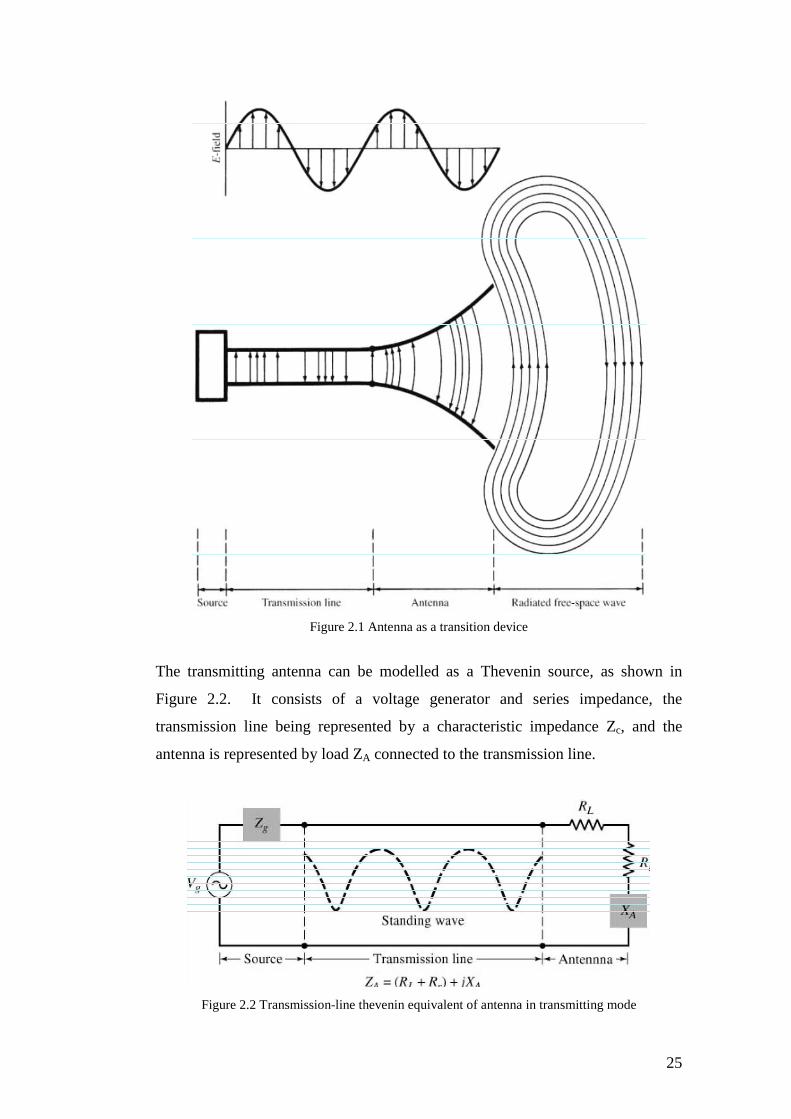
exactly the same from free space to a transmission line. Figure 2.1 shows an
antenna as a transition device [3]. The arrows displayed in Figure 2.1 correspond
to the electric field lines as the wave is transitioned into free space.
25
Figure 2.1 Antenna as a transition device
The transmitting antenna can be modelled as a Thevenin source, as shown in
Figure 2.2. It consists of a voltage generator and series impedance, the
transmission line being represented by a characteristic impedance Zc, and the
antenna is represented by load ZA connected to the transmission line.
Figure 2.2 Transmission-line thevenin equivalent of antenna in transmitting mode

26
Antenna losses due to conductor, dielectric or heat are represented by the loss
resistance, RL. The radiation resistance, Rr, represents the real part of the
radiation impedance of the antenna. The reactance, XA, represents the imaginary
part of the impedance associated with the radiation from the antenna.
2.2 Types of antennas
There are numerous types of antennas developed for many different applications;
they can be classified into four distinct groups.
2.2.1 Wire antennas
Wire antennas are probably the most recognisable, as they are ubiquitous and
typified by TV aerials, car aerials etc. Wire antennas can include dipoles, loops,
helical, sleeve dipoles, Yagi-Uda arrays. Wire antennas generally have low gain
and operate at lower frequencies (HF to UHF). They have the advantages of low
cost, ease of fabrication and simple design.
2.2.2 Aperture antennas
Aperture antennas have a physical opening through which propagating
electromagnetic waves flow. For example, a horn antenna opening acts as a
“funnel” directing the waves into the waveguide. The aperture is usually several
wavelengths long in one or more dimensions. The pattern has a narrow main
beam which leads to high gain. For a fixed aperture size, the main beam pattern
narrows down as frequency increases. These types of antennas are very useful in
aerospace and spacecraft applications, because they can be easily flush-mounted
on the skin of an aircraft or spacecraft. Examples of these antennas include
parabolic reflector, horn antennas, lenses antennas and circular apertures.
2.2.3 Array Antennas
Array antennas are made up of a matrix of discrete sources which radiate
individually. The pattern of the array is determined by the relative amplitude and
phase of the excitation fields of each source and the geometric spacing of the sources.
Typical elements in an array are dipoles, monopoles, slots in waveguides, open-ended
antennas and microstrip radiators.

27
2.2.4 Printed Antennas
Printed antennas can encompass all of the antennas mentioned in sections 2.2.1 to
2.2.3, except they take a planar form. Printed antennas are made via
photolithographic methods, with both the feeding structure and the antenna
fabricated on a dielectric substrate. Printed antennas form the bulk of the
structures discussed in this thesis.
2.3 Radiation Mechanism
All antennas, regardless of type, operate under the same basic principle that
radiation is produced by an acceleration (or deceleration) of electrical charge. To
illustrate the principle, a piece of conducting wire, as shown in Figure 2.3 [4], will
be used.
Figure 2.3. Charge uniformly distributed in a circular cross section cylinder wire
If the electric charge density, ρ, is uniform over the piece of wire, then by
combining Maxwell’s Equations, (2.2) and (2.3), it can be shown that:
Jz = ρ.vz (2.5)
Where Jz is the component of current density,cJr
, in the z-direction and vz is the
velocity in which the charge, Q, is moving within the volume in the z-direction.
If the wire is a perfect conductor then the current resides on the surface of the

28
conductor and current density becomes Js (amperes/m). This is shown by
Equation 2.6.
Js = ρs.vz (2.6)
ρs represents the surface charge density (coulombs/m2). If the wire is very thin, or
zero radius, then Equation 2.6 reduces to:
Iz = ρl.vz (2.7)
Where, ρl (coulombs/m) is the charge per unit length.
If the current varies with time then the derivative of Equation 2.7 can be written
as:
dt
dv
dt
dI zl
z ρ= (2.8)
If the wire is of a length, L, then the Equation 2.8 can be written as:
dt
dvQ
dt
dIL zz = (2.9)
This equation is known as the basic equation of radiation and shows that time-
changing current radiates and accelerated charge radiates. The radiation is
perpendicular to the acceleration of charge, and the radiated power is proportional
to the square of either the right or left hand side of Equation 2.9. For steady state
harmonics the focus is on current and for transients or pulses the focus is on
charge [5]. To create charge acceleration (or deceleration) the wire must be
curved, bent, discontinuous or terminated. Periodic charge acceleration (or
deceleration) or time varying current is also created when charge is oscillating in
a time-harmonic motion. Therefore:
1. If a charge is not moving, current is not created and there is no radiation

29
2. If charge is moving in a uniform velocity:
a. There is no radiation if the wire is straight and infinite in extent
b. There is radiation if the wire is curved, bent, discontinuous, terminated,
or truncated
3. If charge is oscillating in a time-motion, it radiates even if the wire is
straight
2.4 The Dipole
To illustrate the principle of radiation from an antenna it is useful to look at one of
the simplest and one of the most widely used antennas, the dipole. The dipole is
realised by a short straight wire of finite length, which terminates at two points
allowing charge to be collected. If an alternating current generator is connected to
the centre of the wire dipole it can drive charge from one end to the other. This is
illustrated in Figure 2.4 [6].
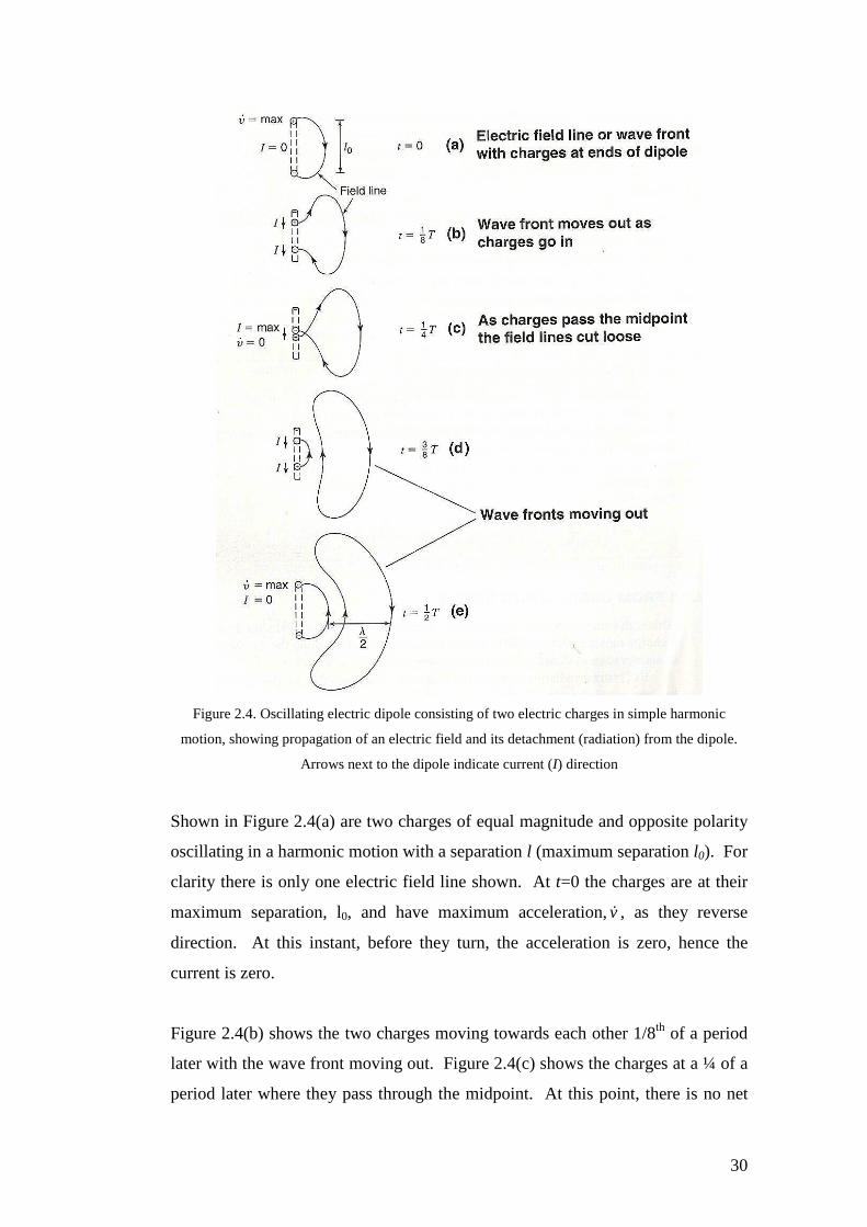
30
Figure 2.4. Oscillating electric dipole consisting of two electric charges in simple harmonic
motion, showing propagation of an electric field and its detachment (radiation) from the dipole.
Arrows next to the dipole indicate current (I) direction
Shown in Figure 2.4(a) are two charges of equal magnitude and opposite polarity
oscillating in a harmonic motion with a separation l (maximum separation l0). For
clarity there is only one electric field line shown. At t=0 the charges are at their
maximum separation, l0, and have maximum acceleration,v& , as they reverse
direction. At this instant, before they turn, the acceleration is zero, hence the
current is zero.
Figure 2.4(b) shows the two charges moving towards each other 1/8th of a period
later with the wave front moving out. Figure 2.4(c) shows the charges at a ¼ of a
period later where they pass through the midpoint. At this point, there is no net
31
charge (the current, I, is at a maximum) on the antenna and as a result the field
line is forced to create its own loop. As time progresses to a ½ period, the fields
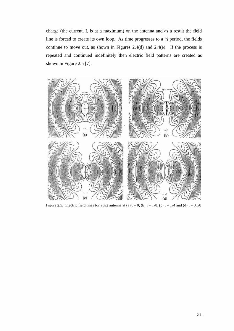
continue to move out, as shown in Figures 2.4(d) and 2.4(e). If the process is
repeated and continued indefinitely then electric field patterns are created as
shown in Figure 2.5 [7].
Figure 2.5. Electric field lines for a λ/2 antenna at (a) t = 0, (b) t = T/8, (c) t = T/4 and (d) t = 3T/8
32
2.5 Antenna Field Region
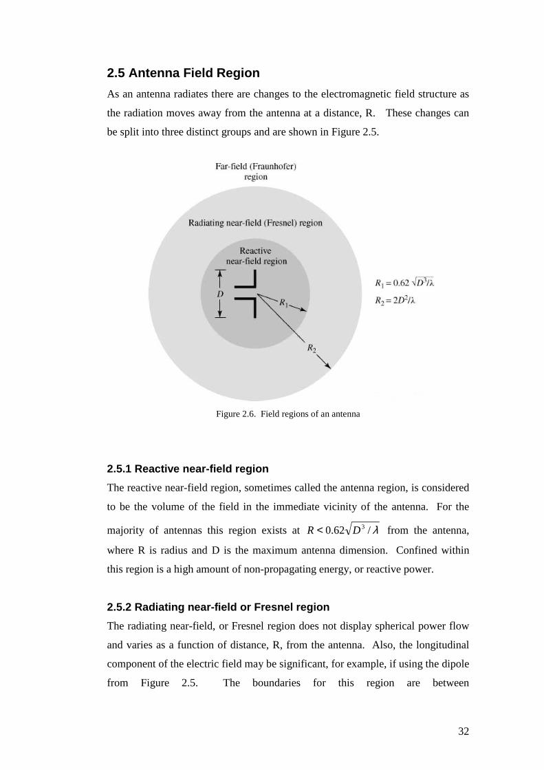
As an antenna radiates there are changes to the electromagnetic field structure as
the radiation moves away from the antenna at a distance, R. These changes can
be split into three distinct groups and are shown in Figure 2.5.
Figure 2.6. Field regions of an antenna
2.5.1 Reactive near-field region
The reactive near-field region, sometimes called the antenna region, is considered
to be the volume of the field in the immediate vicinity of the antenna. For the
majority of antennas this region exists at λ/62.0 3DR < from the antenna,
where R is radius and D is the maximum antenna dimension. Confined within
this region is a high amount of non-propagating energy, or reactive power.
2.5.2 Radiating near-field or Fresnel region
The radiating near-field, or Fresnel region does not display spherical power flow
and varies as a function of distance, R, from the antenna. Also, the longitudinal
component of the electric field may be significant, for example, if using the dipole
from Figure 2.5. The boundaries for this region are between

33
where λ/62.0 3DR ≥ and λ/2 2DR < , and where D is the largest dimension. If
the antenna is very small compared to wavelength this region may not exist.
2.5.3 Radiating far-field or Fraunhofer region
In the radiating far-field or Fraunhofer region the field components are transverse
to the radial direction from the antenna and all the power flow is directed
outwards in a radial fashion. In this region the shape of the field pattern is
independent of the distance, R, from the antenna. The inner boundary is taken to
be the distance λ/2 2DR = , where D is the largest dimension of the antenna.
2.5.4 Characteristic impedance of EM waves
To help differentiate between near-field and far-field regions it is useful to
analyse the characteristic impedance of plane waves. It can be shown [8], that the
characteristic impedance of a plane wave for a lossless medium is given by:
r
r
Z
εεεµµµεµ
0
0
0 )(
==
Ω=
(2.10)
Where:
ε0 = Permittivity of free space = 8.854 x 10⁻¹² (F/m)
εr = Relative permittivity of the dielectric material
µ0 = Permeability of free space = 4π x 10-7 (H/m)
µr = Relative permeability of the magnetic material
For plane waves, this impedance is also known as the intrinsic impedance of the
medium. In free space, where Z0 = 377Ω, the E-field and H-field are orthogonal
to each other and orthogonal to the direction of propagation. If the wave is in the
near-field, in a free space environment, Z0 ≠ 377Ω since the fields are not
orthogonal to each other, or in the direction of propagation.

34
2.5.5 Velocity of Propagation
Another useful differentiation between the far-field and near-field regions, which
gives an insight into the property of electromagnetic waves, is the velocity of
propagation (m/s). The velocity of propagation of a plane wave, sometimes
known as phase velocity, is the speed at which a wave moves through a medium
and is given [9], for a lossless medium, by:
)(1 1−== ms
kp
ωεµ
υ (2.11)
Where:
ω = frequency (radians/s)
β = µεω = wavenumber (m-1)
For a plane wave travelling in free space, the velocity is equal to the speed of
light, c = 2.998 x 10⁸ m/s. As with the wave impedance, for the wave to be planar
(i.e. in the far-field) in free space then the phase velocity must equal the speed of
light.
35
2.6 The fields of a short electric dipole
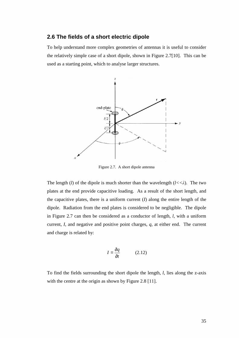
To help understand more complex geometries of antennas it is useful to consider
the relatively simple case of a short dipole, shown in Figure 2.7[10]. This can be
used as a starting point, which to analyse larger structures.
Figure 2.7. A short dipole antenna
The length (l) of the dipole is much shorter than the wavelength (l<< λ). The two
plates at the end provide capacitive loading. As a result of the short length, and
the capacitive plates, there is a uniform current (I) along the entire length of the
dipole. Radiation from the end plates is considered to be negligible. The dipole
in Figure 2.7 can then be considered as a conductor of length, l, with a uniform
current, I, and negative and positive point charges, q, at either end. The current
and charge is related by:
t
qI
∂∂= (2.12)
To find the fields surrounding the short dipole the length, l, lies along the z-axis
with the centre at the origin as shown by Figure 2.8 [11].

36
Figure 2.8. Electric field configuration
Using spherical coordinates, the electric field components (Er, Eθ, Eφ) are
orientated as shown in Figure 2.8. It is assumed that the dipole is in a vacuum. If
the current is flowing in the short dipole shown in Figure 2.9 at some time, t, the
effect of the current is observed at point P, some time later than t.
Figure 2.9. Geometry for a short dipole
As a result, instead of the current being expressed as [12]:
tjeII ω0= (2.13)

37
It should be expressed as:
[ ] [ ])/(0
cstjeII −= ω (2.14)
Where, c is the velocity of light (3x10⁸ ms-1). Adding the r/c factor allows for the
delay in point P sensing the effect of the current due to the velocity of light. This
is known as the retardation effect and the value [I] is known as the retarded
current. This is important as it allows for investigation of the electric and
magnetic fields at the dipole but also many wavelengths away.
To calculate the fields we have to use the retarded vector potential,Ar
. This is the
magnetic vector potential and is useful for solving the EM field generated by a
given harmonic electric current,Jr
. For the dipole in Figure 2.8, the retarded
vector potential only has one component Az. Its value is given as[13]:
[ ]∫
−
=2/
2/
0
4
L
L
z dzs
IA
πµ
(2.15)
Where [I] is the retarded current given by
[ ] [ ])/(0
cstjeII −= ω (2.16)
Where, z = distance to a point on the conductor
I0 = peak value in time of current (uniform along dipole)
µ0 = permeability of free space = 4π x 10-7 Hm-1
To simplify the analysis further consider that point P is very far away from the
dipole (r>>L ). Therefore, s = r and the phase differences of the field
contributions at different parts of the wire can be neglected. The integrand in
Equation 2.15 is then regarded as constant and now becomes:
[ ]
r
eLIA
crtj
z πµ ω
4
)/(00
−
= (2.17)

38
The retarded scalar potential, V, of a charge distribution is:
[ ]∫=V
ds
V τρπε 04
1 (2.18)
Where, [ρ] is the retarded charge density given by:
[ ] [ ])/(0
cstje −= ωρρ (2.19)
and,
dτ = infinitesimal volume element
ε0 = permittivity of free space = 8.85 x 10⁻¹² F/m
The region of charge being considered is confined to the points at the ends of the
dipole, as in Figure 2.8, so (2.18) reduces to:
[ ] [ ]
−=2104
1
s
q
s
qV
πε (2.20)
Combining (2.12) and (2.16):
[ ] [ ] [ ] [ ]ω
ω
j
IdteIdtIq cstj === ∫ ∫ − )/(
0 (2.21)
Substituting (2.21) into (2.20) gives:
[ ] [ ]
−=−−
2
)/(
1
)/(
0
21
4
1
s
e
s
eV
cstjcstj ωω
πε (2.22)
Referring to Figure 2.8, when r>>L , the line connecting the ends of the dipole
and the point P can be considered as parallel so that

39
θcos21
Lrs −= (2.23)
and
θcos21
Lrs += (2.24)
Substituting (2.23) and (2.24) into (2.22) gives:
−−
+=
−
−
2
2
cos
2
cos
0
)/(0
cos2
cos2
4 r
Lre
Lre
j
eIV
c
Lj
c
Lj
crtj θθ
ωπε
θωθω
ω
(2.25)
The L2/4cos2θ term, which was present in the denominator has been omitted since
r>>L . Using de Moivre’s theorem (ejx = cosx + jsinx) Equation 2.25 becomes:
−
−−
+
+=
−
θθωθω
θθωθω
ωπε
ω
cos22
cossin
2
coscos
cos22
cossin
2
coscos
4 20
)/(0
Lr
c
Lj
c
L
Lr
c
Lj
c
L
rj
eIV
crtj
(2.26)
Since the wavelength is much greater than the length of the dipole (λ>>L ) the
following approximations can be made:
1cos
cos2
coscos ≅=
λθπθω L
c
L (2.27)
c
L
c
L
2
cos
2
cossin
θπθω = (2.28)
Combining (2.27) and (2.28) into (2.26), the equation for the scalar potential
reduces to:
( )
+=
−
20
/0 11
4
cos
rj
c
rc
eLIV
crtj
ωπεθ ω
(2.29)

40
The vector (Ar
) and scalar (V) potentials everywhere on a short dipole are
represented by Equations 2.17 and 2.29 respectively. As a result, it is now
possible to determine the electromagnetic fields with the help of Maxwell’s
equations.
Since the magnetic flux,Br
, is solenoidal (divBr
= 0) it can be represented as the
curl of another vector due to the vector identity:
0=×∇⋅∇ Ar
(2.30)
Where,Ar
, is the vector potential. From the relationship between the magnetic
flux density and the magnetic field intensity (Br
=µHr
) Equation 2.31 can be
formed.
AHrr
×∇=µ1
(2.31)
Using Maxwell’s curl equation:
HjErr
ωµ−=×∇ (2.32)
and substituting (2.31) into it gives:
AjErr
×∇−=×∇ ω (2.33)
This can also be written as:
0][ =+×∇ AjErr
ω (2.34)
The scalar potential (V) is the negative derivative of the vector potential ( Ar
).
Using the vector identity:

41
( ) 0=∇−×∇ V (2.35)
We can now get an expression for the electric field:
VAjE ∇−−=rr
ω (2.36)
The next step is to obtain both Er
and Hr
fields in polar coordinates. The vector
potential expressed by polar coordinates is:
φφθθ AaAaAaA rr ˆˆˆ ++=r
(2.37)
The vector potential in this case only has a z-component. Therefore, φA =0 and Ar
and Aθ are given by:
θcoszr AA = (2.38)
θθ sinzAA −= (2.39)
Where Az already been given by 2.17. In polar coordinates the gradient of V is
given by:
φθθ φθ ∂∂+
∂∂+
∂∂=∇ V
ra
V
ra
r
VaV r sin
1ˆ
1ˆˆ (2.40)
As with (2.37) the E-field can be expressed as a sum of its polar coordinate
components:
φφθθ EaEaEaE rr ˆˆˆ ++=r
(2.41)
From (2.36), (2.37) and (2.40) the three spherical coordinate components of the E-
field are:

42
r
VAjE rr ∂
∂−−= ω (2.42)
θω θθ ∂
∂−−= V
rAjE
1 (2.43)
φθω φφ ∂
∂−−= V
rAjE
sin
1 (2.44)
Equation (2.44) reduces to zero, since φA = 0 and V is independent of φ
( 0/ =∂∂ φV ). For Er we substitute (2.38) into (2.42) and for Eθ we substitute
(2.39) into (2.43). This is shown below:
r
VAjE zr ∂
∂−−= θω cos (2.45)
θθωθ ∂
∂−= V
rAjE z
1sin (2.46)
If we re-introduce the previous results for Az (2.17) and V (2.29) into (2.45) and
(2.46) then the following results can be obtained:
[ ]
+=
−
320
)/(0 11
2
cos
rjcr
eLIE
crtj
r ωπεθ ω
(2.47)
[ ]
++=
−
3220
)/(0 11
4
sin
rjcrrc
jeLIE
crtj
ωω
πεθ ω
θ (2.48)
Equations (2.47) and (2.48) are known as the general expressions for the E-field
of a short electric dipole.
The magnetic field may be calculated using Equation (2.31). The curl of Ar
in
polar coordinates is:
∂∂−
∂∂
+
∂∂
−∂∂
+
∂∂
−∂
∂=×∇
θ
θφθφθ
θθ
θφ
φθθφ
r
rr
A
r
rA
r
a
r
ArA
r
arAAr
r
aA
)(ˆ
)sin(
sin
ˆ)()sin(
sin
ˆ2
r
(2.49)

43
Since φA = 0 the first and fourth terms of (2.49) are zero. From (2.17), (2.38) and
(2.39) it can be seen that Ar and Aθ are independent ofφ . As a result the second
and third terms of (2.49) reduce to zero. Only the last two terms in (2.49)
contribute so that Ar
only has a φ component and consequentially by (2.31) so
does the H-field. If we introduce (2.38) and (2.39) into (2.49), and reduce the
terms to zero, then substitute the result into (2.31) the following results are
obtained:
+==−
2
)/(0 1
4
sin
rcr
jeLIHH
crtj ωπ
θ ω
φ
r (2.50)
0== θHH r (2.51)
The results obtained show that a short electric dipole only has three components
Er, Eθ and φH . All the other components are equal to zero. Equations (2.47),
(2.48) and (2.50) can be simplified further for the special case of existing in the
far-field, when r>> λ. The terms 1/r2 and 1/r3 for (2.47),(2.48) and (2.50) can be
omitted. As a result, in the far-field Er ≈ 0, there are only two field components,
Eθ and φH , which are given by:
[ ] [ ]
λθπ
πεωθ ωω
θL
r
eIj
rc
jeLIE
crtjcrtj sin60
4
sin )/(0
20
)/(0
−−
== (2.52)
λθ
πωθ ωω
φL
r
ejI
cr
jeLIH
crtjcrtj sin
4
sin )/(0
)/(0
−−
== (2.53)
Using the ratio Eθ and φH as given by 2.52 and 2.53, the following relationship
can be obtained:
Ω≈Ω=== πεµ
εφ
θ 1207.3761
0
0
0cH
E (2.54)
44
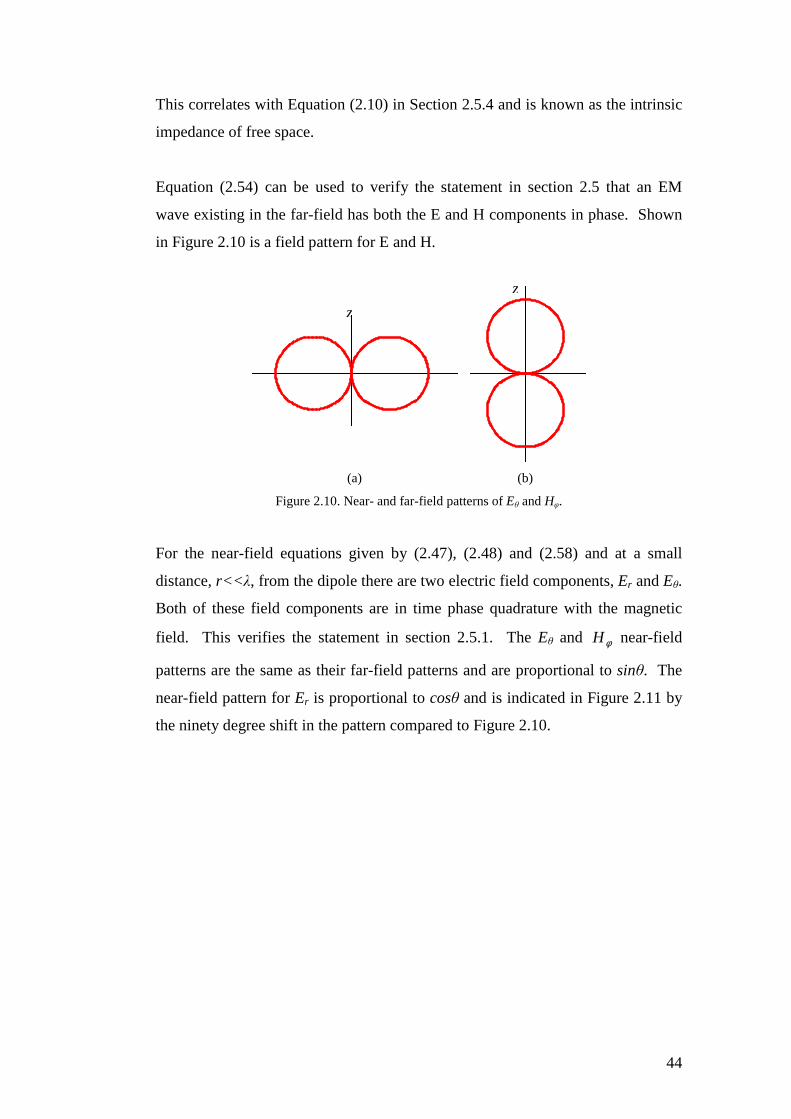
This correlates with Equation (2.10) in Section 2.5.4 and is known as the intrinsic
impedance of free space.
Equation (2.54) can be used to verify the statement in section 2.5 that an EM
wave existing in the far-field has both the E and H components in phase. Shown
in Figure 2.10 is a field pattern for E and H.
(a) (b)
Figure 2.10. Near- and far-field patterns of Eθ and Hφ.
For the near-field equations given by (2.47), (2.48) and (2.58) and at a small
distance, r<< λ, from the dipole there are two electric field components, Er and Eθ.
Both of these field components are in time phase quadrature with the magnetic
field. This verifies the statement in section 2.5.1. The Eθ and φH near-field
patterns are the same as their far-field patterns and are proportional to sinθ. The
near-field pattern for Er is proportional to cosθ and is indicated in Figure 2.11 by
the ninety degree shift in the pattern compared to Figure 2.10.
z
z

45
Figure 2.11. Near-field pattern for Er component
2.7 The fields of a finite length dipole
The previous section explained the theory behind obtaining field plots for a short
dipole. The theory obtained can now be used to obtain data on finite length
dipoles, which will allow for a better understanding of some of the properties of
the antennas investigated in this thesis.
The dipole under analysis in this section is presumed to have a diameter much
smaller than the operating wavelength (d<<λ). This allows the assumption that
the current distribution along the dipole is sinusoidal given that it is fed at its
centre by a balanced 2 wire transmission line. This approximation is considered
suitable as there is no major discrepancy in the far-field patterns for the antennas
investigated later in this thesis.
Examples of current distribution on a range of dipoles of a length up to 2λ are
shown in Figure 2.12 [14].
z
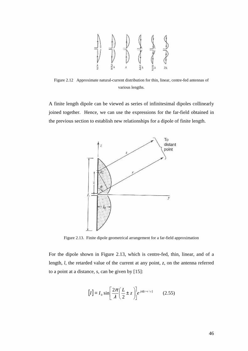
46
Figure 2.12 Approximate natural-current distribution for thin, linear, centre-fed antennas of
various lengths.
A finite length dipole can be viewed as series of infinitesimal dipoles collinearly
joined together. Hence, we can use the expressions for the far-field obtained in
the previous section to establish new relationships for a dipole of finite length.
Figure 2.13. Finite dipole geometrical arrangement for a far-field approximation
For the dipole shown in Figure 2.13, which is centre-fed, thin, linear, and of a
length, l, the retarded value of the current at any point, z, on the antenna referred
to a point at a distance, s, can be given by [15]:
[ ] ]/[0 2
2sin crtjez
LII −
±= ω
λπ
(2.55)
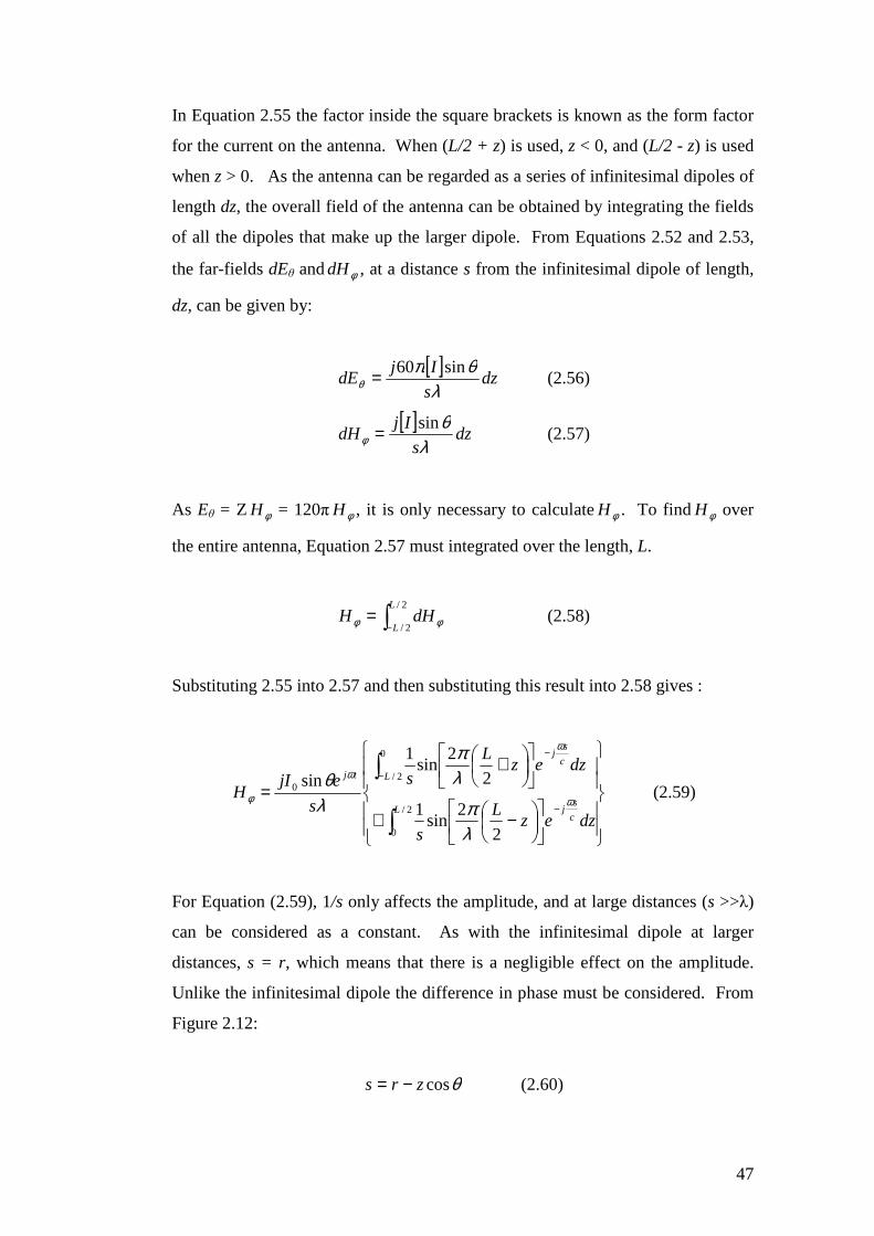
47
In Equation 2.55 the factor inside the square brackets is known as the form factor
for the current on the antenna. When (L/2 + z) is used, z < 0, and (L/2 - z) is used
when z > 0. As the antenna can be regarded as a series of infinitesimal dipoles of
length dz, the overall field of the antenna can be obtained by integrating the fields
of all the dipoles that make up the larger dipole. From Equations 2.52 and 2.53,
the far-fields dEθ and φdH , at a distance s from the infinitesimal dipole of length,
dz, can be given by:
[ ]dz
s
IjdE
λθπ
θsin60= (2.56)
[ ]dz
s
IjdH
λθ
φsin= (2.57)
As Eθ = Z φH = 120π φH , it is only necessary to calculateφH . To find φH over
the entire antenna, Equation 2.57 must integrated over the length, L.
∫−=2/
2/
L
LdHH φφ (2.58)
Substituting 2.55 into 2.57 and then substituting this result into 2.58 gives :
−+
+=
−
−
−
∫
∫
dzezL
s
dzezL
s
s
ejIH
c
sjL
c
sj
Ltj
ω
ω
ω
φ
λπ
λπ
λθ
2
2sin
1
2
2sin
1
sin
2/
0
0
2/0 (2.59)
For Equation (2.59), 1/s only affects the amplitude, and at large distances (s >>λ)
can be considered as a constant. As with the infinitesimal dipole at larger
distances, s = r, which means that there is a negligible effect on the amplitude.
Unlike the infinitesimal dipole the difference in phase must be considered. From
Figure 2.12:
θcoszrs −= (2.60)

48
Substituting (2.60) into (2.59) gives:
−+
+=
−
−
−−
∫
∫
dzezL
dzezL
r
ejIH
zc
jL
zc
j
Lcrtj
θω
θω
ω
φ
λπ
λπ
λθ
cos2/
0
cos0
2/)/(0
2
2sin
2
2sin
2
sin (2.61)
As β = ω / c = 2π / λ, and β / 4π =½λ, Equation 2.61 can be rewritten as:
−+
+=
∫
∫−−
dzzL
e
dzzL
e
r
eIjH
L zj
L
zj
crtj
2
2sin
2sin
2
sin
2/
0
cos
0
2/
cos
)/(0
λπ
β
λθβ
θβ
θβω
φ (2.62)
As the integrals take the form:
∫ +−++
=+ )]cos()sin([)sin(22
bxcbbxcaba
edxbxce
axax (2.63)
For the first integral:
θβ cosja =
β=b
2/Lc β=
For the second integral, a and c are the same as the first integral, but b = -β.
Integrating and simplifying 2.62 yields:
[ ] ( ) ( )( )
−=θ
βθβπφ sin
2/cos2/coscos
20 LL
r
IjH (2.64)
To obtain Eθ, φH is multiplied by Z = 120π, which gives:

49
[ ] ( ) ( )( )
−=θ
βθβθ sin
2/cos2/coscos60 0 LL
r
IjE (2.65)
Where, [ ] )/(00
crtjeII −= ω .
Equations 2.64 and 2.65 give the far-field expressions of φH and Eθ respectively
for a symmetrical, centre-fed, thin dipole of length, L. The expression in the
brackets known as the pattern factor gives the far-field pattern. Shown in Figure
2.14 are polar plots for various lengths of antenna.
(a) (b)
(c) (d)
(e) (f)
Figure 2.14. Polar plots for the radiation patterns of a dipole of length (a) 0.5λ (b) 0.75λ (c) 1λ
(d) 1.25λ (e) 1.5λ (f) 1.75λ

50
As the radiation mechanism and the radiated fields from thin linear dipoles have
been investigated the next stage is to investigate the fundamental limitations of
small antennas.
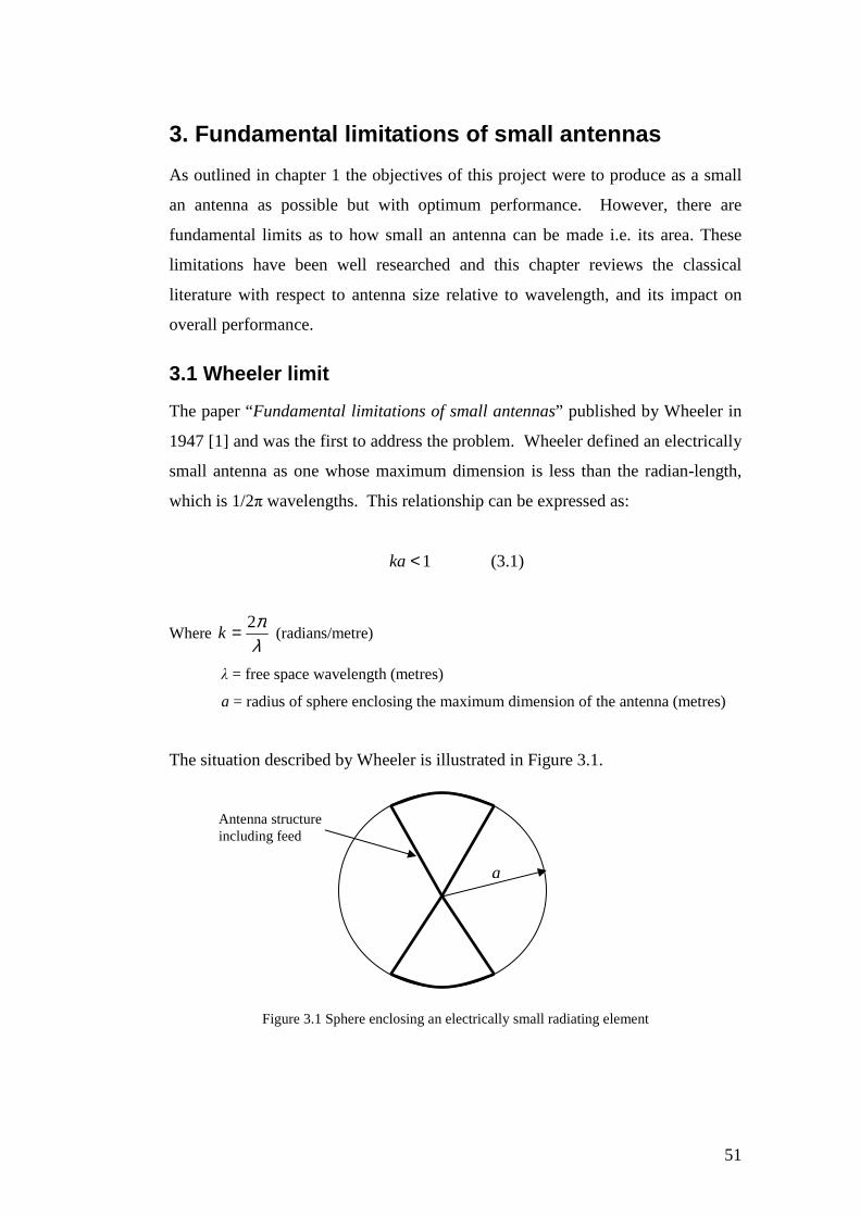
51
3. Fundamental limitations of small antennas
As outlined in chapter 1 the objectives of this project were to produce as a small
an antenna as possible but with optimum performance. However, there are
fundamental limits as to how small an antenna can be made i.e. its area. These
limitations have been well researched and this chapter reviews the classical
literature with respect to antenna size relative to wavelength, and its impact on
overall performance.
3.1 Wheeler limit
The paper “Fundamental limitations of small antennas” published by Wheeler in
1947 [1] and was the first to address the problem. Wheeler defined an electrically
small antenna as one whose maximum dimension is less than the radian-length,
which is 1/2π wavelengths. This relationship can be expressed as:
1<ka (3.1)
Where λπ2=k (radians/metre)
λ = free space wavelength (metres)
a = radius of sphere enclosing the maximum dimension of the antenna (metres)
The situation described by Wheeler is illustrated in Figure 3.1.
Figure 3.1 Sphere enclosing an electrically small radiating element
a
Antenna structure including feed

52
The electrically small antenna is considered to be in free space and enclosed by a
sphere of radius a. The papers published by Wheeler [1], [2] derived the limits of
a small dipole and a small loop (used as a magnetic dipole) from the limitations of
a capacitor and an inductor, respectively. The capacitor and inductor were chosen
to occupy, respectively, volumes equal to those of the dipole and the loop. For
both these cases, Wheeler calculated a radiation power factor and hence the
maximum power factor achievable by the antenna. The power factor is
proportional to the antenna volume, V, and a shape factor. The nominal
bandwidth is given as the power factor p multiplied by the resonant frequency (f0)
and is described by the following relationship.
0f
fpV
∆αα (3.2)
Where cereacantenna
ceresisantennap
tan
tan=
Further investigations of antenna size versus bandwidth capability were further
investigated by L.J. Chu[3], and then by Roger Harrington. The following section
investigates their work.
3.2 Chu-Harrington Limit
A different approach to that of Wheeler was taken by Chu [3]. Chu considered the
field outside the sphere, as shown in Figure 3.1, is a result of an arbitrary current
or source distribution inside the sphere. However, the field outside the sphere can
be expressed as a complete set of orthogonal spherical vector waves propagating
radially outward. Outside the spherical shell Chu assumed that the fields could be
represented by a superposition of orthogonal spherical modes, each with their own
wave impedance. Chu was able to construct a circuit, as depicted by Figure 3.2
(a) [4], with the same impedance and analyse the resonant behaviour of the
antenna.
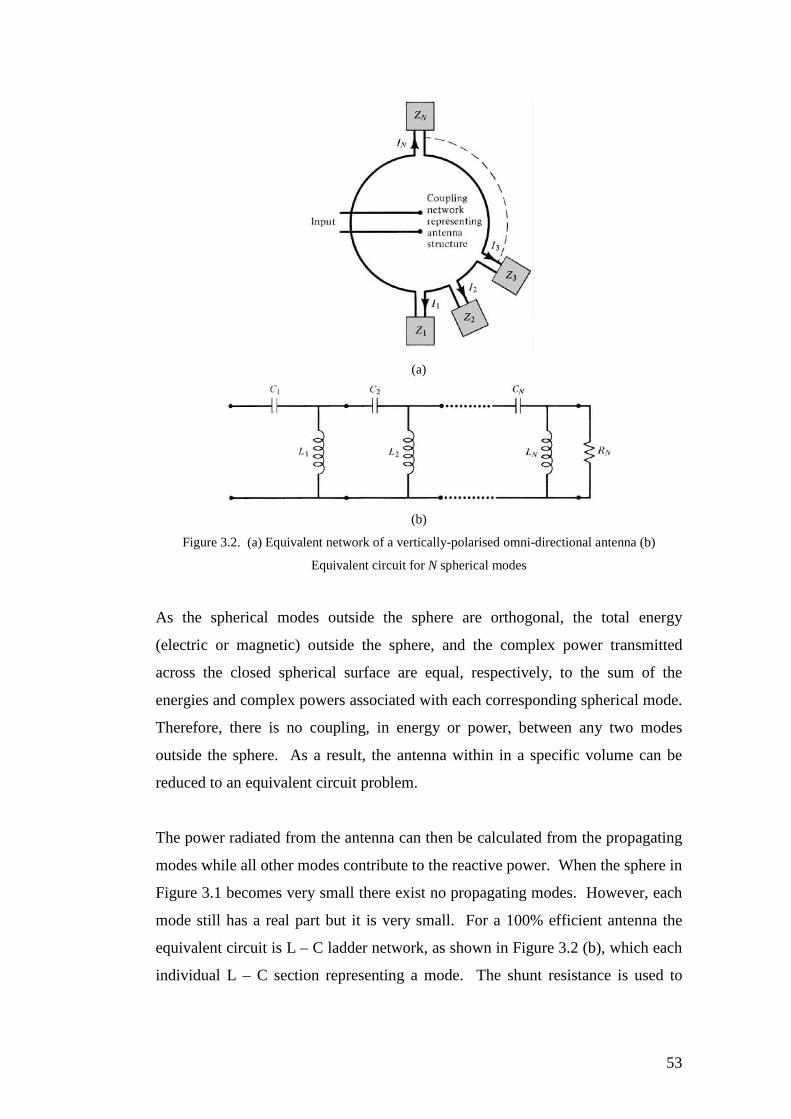
53
(a)
(b)
Figure 3.2. (a) Equivalent network of a vertically-polarised omni-directional antenna (b)
Equivalent circuit for N spherical modes
As the spherical modes outside the sphere are orthogonal, the total energy
(electric or magnetic) outside the sphere, and the complex power transmitted
across the closed spherical surface are equal, respectively, to the sum of the
energies and complex powers associated with each corresponding spherical mode.
Therefore, there is no coupling, in energy or power, between any two modes
outside the sphere. As a result, the antenna within in a specific volume can be
reduced to an equivalent circuit problem.
The power radiated from the antenna can then be calculated from the propagating
modes while all other modes contribute to the reactive power. When the sphere in
Figure 3.1 becomes very small there exist no propagating modes. However, each
mode still has a real part but it is very small. For a 100% efficient antenna the
equivalent circuit is L – C ladder network, as shown in Figure 3.2 (b), which each
individual L – C section representing a mode. The shunt resistance is used to

54
represent the normalised antenna radiation resistance. Using the circuit in Figure
3.2 (b) the input impedance can be found.
When the sphere in Figure 3.1 is very small the quality factor, Q, becomes very
large, since the Q of each individual mode is a ratio of its stored energy to
radiated energy. It has been reported by Hansen [5] and Mclean [6] that the
higher order modes become evanescent when 1<ka . As a result, the quality
factor for only the lowest order TMn0 mode i.e. corresponds to the fields of a point
dipole is required. Chu’s expression is therefore:
( )( ) ( )[ ]23
2
1
21
kaka
kaQ
++= (3.3)
If 1<<ka then ( )3
1
kaQ ≈
If two modes are excited i.e. TE and TM, the values of Q are halved. The lowest
achievable Q is related to the largest dimension linear dimension of an electrically
small antenna, highlighted by equation 3.3. The Q is independent of the
geometrical layout of the antenna structure within the sphere, shown in Figure
3.1. The geometrical layout only impacts on the type of mode being excited, such
as TE, TM or TE and TM. Therefore equation 3.3 represents the fundamental
limit on the electrical size of an antenna. Practically, this limit is only approached
but is never exceeded or even equalled.
The Q is also related to the fractional bandwidth of the system by the following
equation 3.4:
Fractional bandwidth = FBW = Qf
f 1
0
=∆ (3.4)
where f0 = centre frequency
f∆ = bandwidth
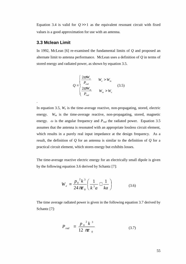
55
Equation 3.4 is valid for 1>>Q as the equivalent resonant circuit with fixed
values is a good approximation for use with an antenna.
3.3 Mclean Limit
In 1992, McLean [6] re-examined the fundamental limits of Q and proposed an
alternate limit to antenna performance. McLean uses a definition of Q in terms of
stored energy and radiated power, as shown by equation 3.5.
>
>=
emrad
m
merad
e
WWP
W
WWP
W
Qω
ω
2
2
(3.5)
.
In equation 3.5, We is the time-average reactive, non-propagating, stored, electric
energy. Wm is the time-average reactive, non-propagating, stored, magnetic
energy. ω is the angular frequency and Prad the radiated power. Equation 3.5
assumes that the antenna is resonated with an appropriate lossless circuit element,
which results in a purely real input impedance at the design frequency. As a
result, the definition of Q for an antenna is similar to the definition of Q for a
practical circuit element, which stores energy but exhibits losses.
The time-average reactive electric energy for an electrically small dipole is given
by the following equation 3.6 derived by Schantz [7]:
+=kaak
kpWe
11
24 30
320
πε (3.6)
The time average radiated power is given in the following equation 3.7 derived by
Schantz [7]:
0
320
12 πεkp
Prad = (3.7)

56
Substituting equations 3.6 and 3.7 into equation 3.5 yields McLean’s expression
for the Q of an electrically small dipole:
kaak
kpkaak
kp
P
WQ
rad
e
11
1211
242
2
3
320
03
0
320
+=
+==ωπε
πεωω
(3.8)
3.4 Fundamental Limits of a 5.8 GHz antenna
To give some substance to the theory described in the previous sections, an
example will be given for an antenna operating at 5.8 GHz. Using the following
procedure it is possible to calculate the radius for the Wheeler sphere shown in
Figure 3.1.
mmf
c69.51
108.5
10998.29
8
=×
×==λ (3.9)
475.12105169.0
22 === πλπ
k (3.10)
mmk
a 232.8475.121
11 ==< (3.11)
The result of equation 3.11 shows that for an antenna to be electrically small at
5.8 GHz it must be occupy a spherical volume with a radius no greater than
8.232mm.
Using a small electrical dipole, of length equal to 0.1λ, it is possible to calculate
values for the theoretical maximum gain [8], minimum Q (Eqn 3.8) and maximum
bandwidth (Eqn 3.4) as follows:
dBikakaG 726.0)(2)( 2max =+= (3.12)
5.3511
3min =+=kaak
Q (3.13)
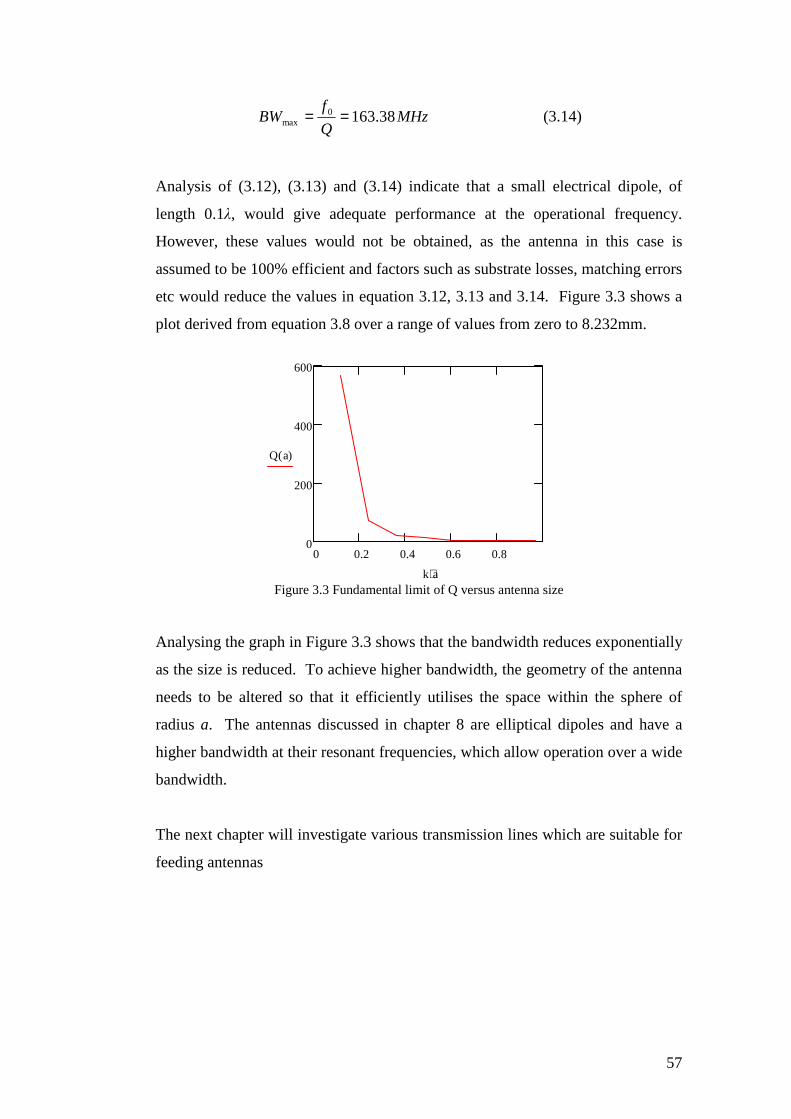
57
MHzQ
fBW 38.1630
max == (3.14)
Analysis of (3.12), (3.13) and (3.14) indicate that a small electrical dipole, of
length 0.1λ, would give adequate performance at the operational frequency.
However, these values would not be obtained, as the antenna in this case is
assumed to be 100% efficient and factors such as substrate losses, matching errors
etc would reduce the values in equation 3.12, 3.13 and 3.14. Figure 3.3 shows a
plot derived from equation 3.8 over a range of values from zero to 8.232mm.
Figure 3.3 Fundamental limit of Q versus antenna size
Analysing the graph in Figure 3.3 shows that the bandwidth reduces exponentially
as the size is reduced. To achieve higher bandwidth, the geometry of the antenna
needs to be altered so that it efficiently utilises the space within the sphere of
radius a. The antennas discussed in chapter 8 are elliptical dipoles and have a
higher bandwidth at their resonant frequencies, which allow operation over a wide
bandwidth.
The next chapter will investigate various transmission lines which are suitable for
feeding antennas
0 0.2 0.4 0.6 0.80
200
400
600
Q a( )
k a⋅
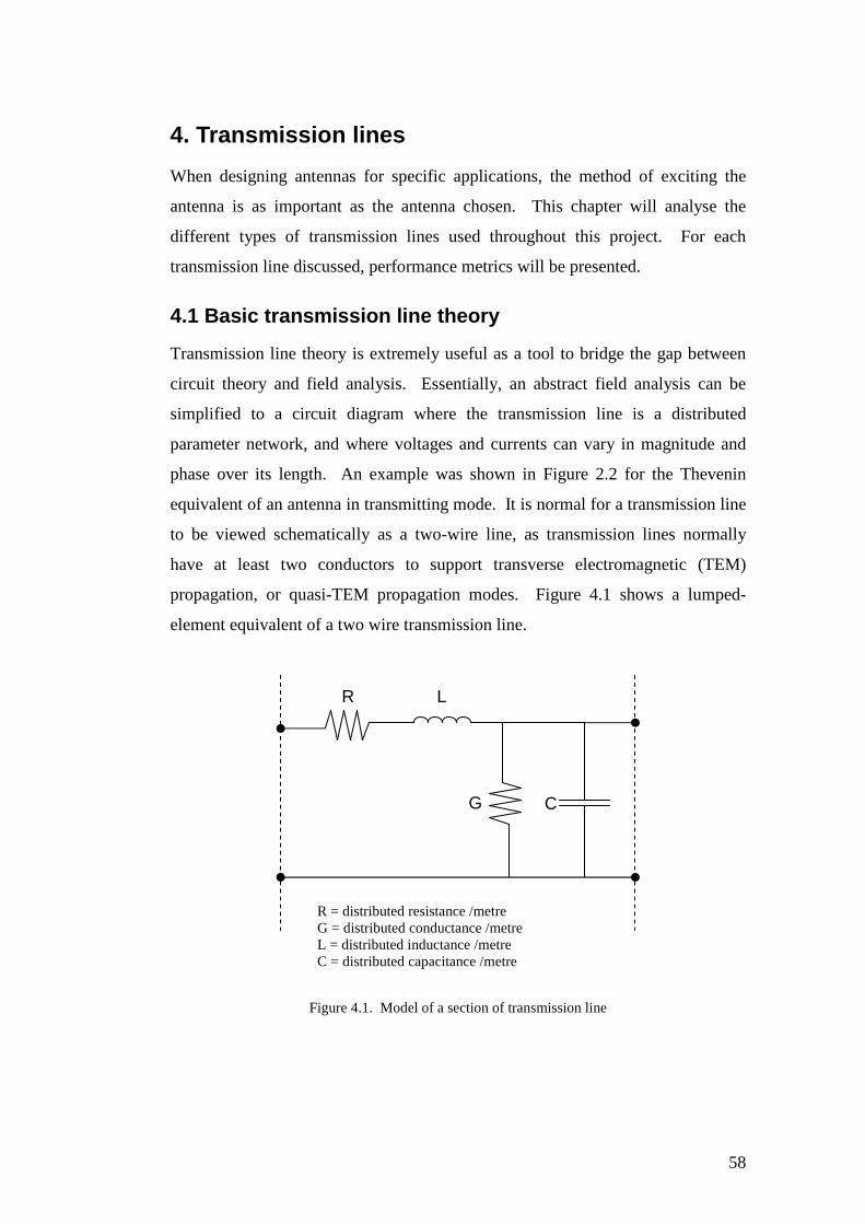
58
4. Transmission lines
When designing antennas for specific applications, the method of exciting the
antenna is as important as the antenna chosen. This chapter will analyse the
different types of transmission lines used throughout this project. For each
transmission line discussed, performance metrics will be presented.
4.1 Basic transmission line theory
Transmission line theory is extremely useful as a tool to bridge the gap between
circuit theory and field analysis. Essentially, an abstract field analysis can be
simplified to a circuit diagram where the transmission line is a distributed
parameter network, and where voltages and currents can vary in magnitude and
phase over its length. An example was shown in Figure 2.2 for the Thevenin
equivalent of an antenna in transmitting mode. It is normal for a transmission line
to be viewed schematically as a two-wire line, as transmission lines normally
have at least two conductors to support transverse electromagnetic (TEM)
propagation, or quasi-TEM propagation modes. Figure 4.1 shows a lumped-
element equivalent of a two wire transmission line.
Figure 4.1. Model of a section of transmission line
R L
G C
R = distributed resistance /metre G = distributed conductance /metre L = distributed inductance /metre C = distributed capacitance /metre

59
Figure 4.1 illustrates that the series resistance models conductive losses while the
conductance or shunt resistance models substrate losses. Using the model shown
in Figure 4.1 [1] the characteristic impedance, Z0, of the line is given by:
CjG
LjRZ
ωω
++=0 (4.1)
For an ideal lossless line, Equation 4.1 reduces to:
C
LZ =0 (4.2)
4.2 Transmission Lines
When designing microwave circuits, there are many possible transmission lines
that can be used to feed antennas, or to connect individual components together.
This section briefly describes the orientation of the fields, derivation of the
characteristic impedance and the effective wavelength.
4.2.1 Two-wire transmission line
Equation 4.2 is valid for a lossless two-wire transmission line as it can propagate
TEM waves. Figure 4.4(a) shows the orientation of the EM fields in such a two-
wire system. Quite often, the values of L and C are not known, but the physical
dimensions (conductor diameter, spacing, dielectric properties, etc.) of the line are
known. The following formula can be used to determine the characteristic
impedance of a two-wire transmission line [2].
a
DZ
r
2ln
1200 ε
π= (4.3)
Where,
εr is the relative dielectric constant of the material between the two conductors
D is the centre-to-centre separation of the two conductors
a is the diameter of the wires
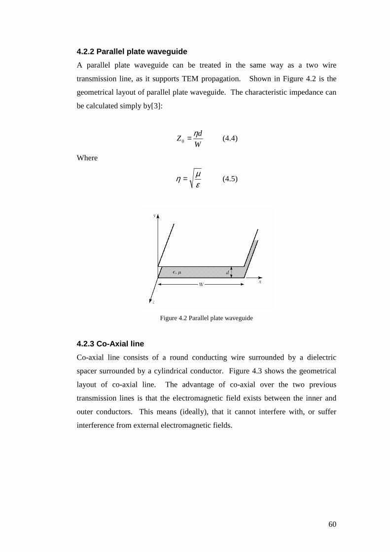
60
4.2.2 Parallel plate waveguide
A parallel plate waveguide can be treated in the same way as a two wire
transmission line, as it supports TEM propagation. Shown in Figure 4.2 is the
geometrical layout of parallel plate waveguide. The characteristic impedance can
be calculated simply by[3]:
W
dZ
η=0 (4.4)
Where
εµη = (4.5)
Figure 4.2 Parallel plate waveguide
4.2.3 Co-Axial line
Co-axial line consists of a round conducting wire surrounded by a dielectric
spacer surrounded by a cylindrical conductor. Figure 4.3 shows the geometrical
layout of co-axial line. The advantage of co-axial over the two previous
transmission lines is that the electromagnetic field exists between the inner and
outer conductors. This means (ideally), that it cannot interfere with, or suffer
interference from external electromagnetic fields.
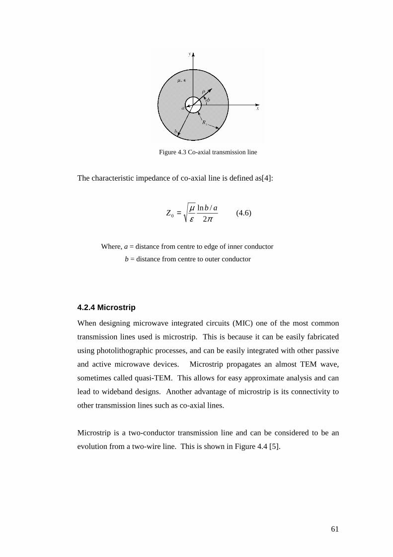
61
Figure 4.3 Co-axial transmission line
The characteristic impedance of co-axial line is defined as[4]:
πεµ
2
/ln0
abZ = (4.6)
Where, a = distance from centre to edge of inner conductor
b = distance from centre to outer conductor
4.2.4 Microstrip
When designing microwave integrated circuits (MIC) one of the most common
transmission lines used is microstrip. This is because it can be easily fabricated
using photolithographic processes, and can be easily integrated with other passive
and active microwave devices. Microstrip propagates an almost TEM wave,
sometimes called quasi-TEM. This allows for easy approximate analysis and can
lead to wideband designs. Another advantage of microstrip is its connectivity to
other transmission lines such as co-axial lines.
Microstrip is a two-conductor transmission line and can be considered to be an
evolution from a two-wire line. This is shown in Figure 4.4 [5].
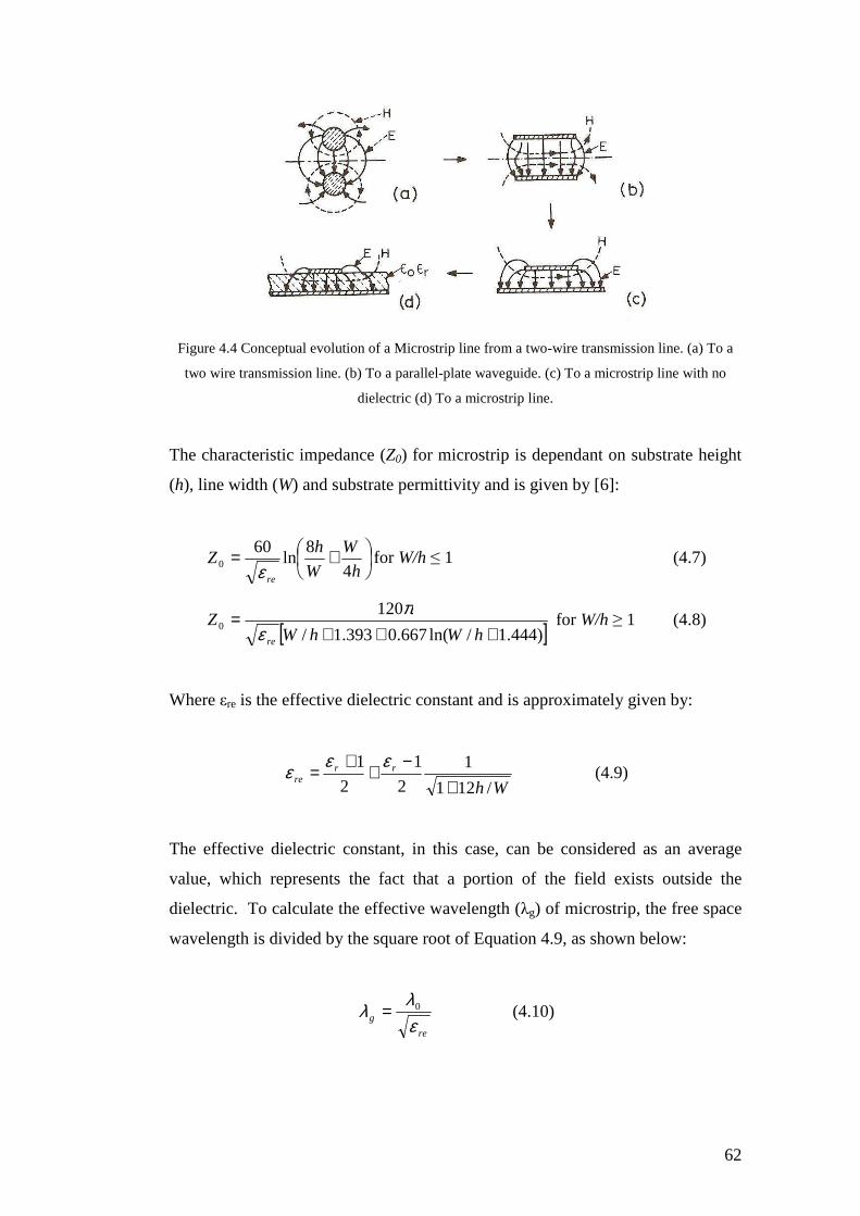
62
Figure 4.4 Conceptual evolution of a Microstrip line from a two-wire transmission line. (a) To a
two wire transmission line. (b) To a parallel-plate waveguide. (c) To a microstrip line with no
dielectric (d) To a microstrip line.
The characteristic impedance (Z0) for microstrip is dependant on substrate height
(h), line width (W) and substrate permittivity and is given by [6]:
+=h
W
W
hZ
re4
8ln
600 ε
for W/h ≤ 1 (4.7)
[ ])444.1/ln(667.0393.1/
1200 +++
=hWhW
Zreε
π for W/h ≥ 1 (4.8)
Where εre is the effective dielectric constant and is approximately given by:
Whrr
re/121
1
2
1
2
1
+−
++
=εεε (4.9)
The effective dielectric constant, in this case, can be considered as an average
value, which represents the fact that a portion of the field exists outside the
dielectric. To calculate the effective wavelength (λg) of microstrip, the free space
wavelength is divided by the square root of Equation 4.9, as shown below:
re
g ελλ 0= (4.10)
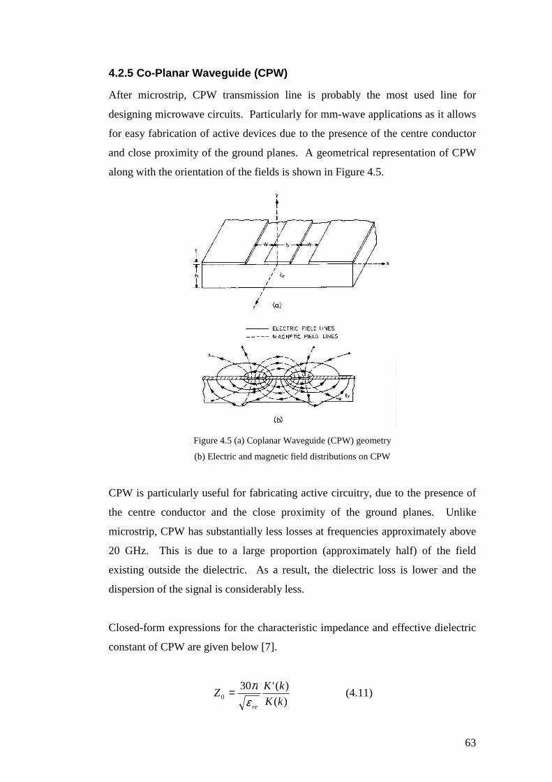
63
4.2.5 Co-Planar Waveguide (CPW)
After microstrip, CPW transmission line is probably the most used line for
designing microwave circuits. Particularly for mm-wave applications as it allows
for easy fabrication of active devices due to the presence of the centre conductor
and close proximity of the ground planes. A geometrical representation of CPW
along with the orientation of the fields is shown in Figure 4.5.
Figure 4.5 (a) Coplanar Waveguide (CPW) geometry
(b) Electric and magnetic field distributions on CPW
CPW is particularly useful for fabricating active circuitry, due to the presence of
the centre conductor and the close proximity of the ground planes. Unlike
microstrip, CPW has substantially less losses at frequencies approximately above
20 GHz. This is due to a large proportion (approximately half) of the field
existing outside the dielectric. As a result, the dielectric loss is lower and the
dispersion of the signal is considerably less.
Closed-form expressions for the characteristic impedance and effective dielectric
constant of CPW are given below [7].
)(
)('300 kK
kKZ
reεπ= (4.11)

64
Where, WS
Sk
2+=
The ratio K/K’ can be defined as:
−+=
k
k
kK
kK
1
12ln
1
)('
)(
π for 0.707 ≤ k ≤ 1 (4.12)
−+
=
'1
'12ln
)('
)(
k
kkK
kK π for 0 ≤ k ≤ 0.707 (4.13)
The effective permittivity can be obtained using the following formula:
+−+−+
++
=)25.0)(1.01(01.07.004.0
75.1)/log(785.1tanh
2
1
kkh
kW
Wh
r
rre ε
εε (4.14)
This formula gives accuracy of 1.5 percent for h/W ≥ 1. A good rule of thumb for
effective permittivity is that value should be approximately the average of
dielectric permittivity and air ((εr+1)/2), as the field approximately exists, half in
the dielectric, and half in the air.
4.2.6 Slotline
Slotline was first introduced in 1968 by Cohn [8] as a transmission structure for
microwave integrated circuits (MIC’s). The basic slotline structure is shown in
Figure 4.6.
Figure 4.6 Slotline transmission line

65
Slotline consists of two parallel strips of metal separated by a narrow slot on top
of a dielectric substrate. Normally, there is no metal on the underside. For MIC
design, slotline is regarded as the third choice of transmission line and is only
used when microstrip and CPW cannot meet the design requirements. Generally,
it is only used in hybrid combinations with microstrip and CPW, an example of
this is shown in chapter 9 when a CPW-to-slotline transition is used to give a
balance feed to a dipole antenna.
In slotline, the wave propagates along the slot with the major electric field
component situated across the slot. The mode of propagation is non-TEM and
can be considered to be transverse electric (TE). Figure 4.7 shows the field
distributions for slotline [9].
Figure 4.7. Field distribution of slotline. Solid line is E-field and dashed line is H-field.
As shown in Figure 4.7 a portion of the field exists outside the dielectric. For an
infinitely thick dielectric the effective wavelength can be given by:
2
1+= rre
εε (4.14)
re
g ελλ 0= (4.15)
x
y

66
It has been shown [10] that these conditions hold for a finite thickness substrate
(h) when using the following equation:
1/25.00
−=
r
c
h ελ
(4.16)
This relationship is used to derive the cut-off frequency for TE10 surface wave
mode and indicates the minimum height required for Equation 4.14 to hold. For
the majority of cases, the value of effective permittivity will be much lower than
the average of air and the dielectric constant. As an example, for an operating
frequency of 5.8 GHz and a substrate with a relative permittivity of 12.9 the
minimum height would have to be 3.75mm, which is well above the majority of
general substrate heights at this frequency range. The effective wavelength can
be calculated theoretically but they are complex, and unlike microstrip, as it is a
function of free space wavelength due to the transverse electric mode that is
present.
Calculating the slotline impedance is complex, for the same reasons as calculating
the effective wavelength. The characteristic impedance cannot be defined
uniquely due to the non-TEM propagation. A useful definition for the
characteristic impedance (Z0) is given by:
P
VZ
2
2
0 = (4.17)
Where V is the peak voltage across the slot and P is the average power.
Now that both a simple antenna and its possible transmission lines have been
discussed the next step is to investigate the fundamental parameters used to
characterise an antennas performance. These parameters are now discussed in the
following section.

67
5. Antenna Analysis
To understand the challenges faced when designing antennas it is necessary to
provide some background information on some of the key parameters and
performance metrics. There are many antenna types with differing geometry but
there are certain fundamental parameters can be used to describe all of them.
Also discussed in this chapter is Ansoft’s High Frequency Simulation Software
(HFSS), which was used to design and simulate antennas investigated in this
project.
5.1 Fundamental Antenna Parameters
The most fundamental antenna parameters are;
1. Impedance Bandwidth
2. S-parameters
3. Radiation pattern
4. Directivity
5. Efficiency
6. Gain
7. Polarisation
All of the parameters mentioned above are necessary to fully characterise an
antenna, and to establish whether the antenna is optimised for its purpose.
5.1.1 Impedance Bandwidth
The term ‘impedance bandwidth’ is used to describe the bandwidth over which
the antenna has acceptable losses due to mismatch. The impedance bandwidth
can be measured by the characterisation of both the Voltage Standing Wave Ratio
(VSWR) and Return Loss (RL) at the frequency band of interest. Both VSWR
and RL are dependant on measuring the reflection coefficient (Γ). Γ is defined as
the ratio of the amplitude of the reflected voltage wave (V0-) normalised to the
amplitude of the incident voltage wave (V0+) at a load [1]. Γ can also be defined
by using other field or circuit quantities and is defined by the following equation.

68
−
+
=Γ0
0
V
V (5.1)
The VSWR is defined as the ratio between the voltage maximum and voltage
minimum of the standing wave created by the mismatch at the load on a
transmission line. The VSWR equation is shown in Equation 5.2.
Γ−Γ+
==1
1
0Z
ZVSWR L (5.2)
The return loss (RL) is the magnitude of the ratio of the reflected wave to that of
the incident wave, and is defined in dB as:
Γ−= LogRL 20 (5.3)
The scattering parameter S11 is equivalent to Γ. It is common for S11 to be defined
in dB as:
Γ= LogS 2011 (5.4)
The maximum acceptable mismatch for an antenna is normally 10% of the
incident signal. For the reflection coefficient, this equates to Γ = 0.3162. For
VSWR the impedance bandwidth lies between 1< VSWR< 2, and for Return Loss
its value must be greater than 10dB or S11 < -10 dB. A description of S-
parameters follows is given in the following section.
5.1.2 S-Parameters
When designing antennas as part of a network, or on their own, it is advantageous
to create a model which allows the designer insight into the performance of the
system/antenna. It is common to extract useful data via a Vector Network
Analyser (VNA). The data is normally presented in the form of S-parameters. At
low frequencies, simple circuit models normally suffice but at high frequencies a

69
distributed model is needed to account for a variety of possible physical effects,
such as:
• Skin depth )/2( ωµσδ =
• Energy propagation
• Radiation
• Reflections / Transmission
• Fringing fields (coupling)
• Energy splitting / combining
Also S-parameters enable broadband characterisation unlike impedance and
admittance parameters, which need open or short-circuit terminations to
characterise and are not conducive to broadband characterisation.
The S-parameters allow for a complete description of a N-port network as seen at
its N-ports in Figure 5.1.
Figure 5.1 An N-Port network
The S-Parameters are defined by measuring the voltage travelling waves between
the N-ports. To explain this concept it is best to look at a two port network, as
shown by Figure 5.2.
N-Port Network
PORT 1
PORT 2
PORT N

70
V1 = Voltage at port 1 a1 = signal incident at port 1
V2 = Voltage at port 2 b1 = signal reflected at port 1
I1 = Current at port 1 a2 = signal incident at port 2
I2 = Current at port 2 b2 = signal reflected at port 2
Z0 = Characteristic impedance
Z1 = port 1 impedance
Z2 = port 2 impedance
Figure 5.2 Two port network definition
It is also important to define the incident and reflected signals, which take the
form:
)(0
wattsZ
Va
x
x
+
= (5.5)
)(0
wattsZ
Vb
x
x
−
= (5.6)
Combing equations 5.5 and 5.6 we get four possible results.
• The input reflection coefficient, when port 2 is matched, 01
111
2 =
=a
a
bS
• The reverse transmission gain, when port 1 is matched, 02
112
1=
=a
a
bS
• The output reflection coefficient, when port 1 is matched, 02
222
1=
=a
a
bS
• The forward transmission gain, when port 2 is matched, 01
221
2 =
=a
a
bS
Two-port network
I2 I1
V1 V2
a1
b1 b2
a2
Z0 Z0 Z1 Z2

71
Typically, when using S-parameters to characterise antennas the reflection
coefficients and forward transmission gain are most frequently used. Ideally
reflection coefficients should tend towards zero (S11=S22=0) as this means that
there is no power being reflected back due to a good match to the characteristic
impedance of the feeding structures, usually 50Ω. The forward transmission gain
should ideally tend towards one, but this is generally not the case for low gain
antennas where the path loss can be 20dB or greater.
It is normal to express the S-parameters in terms of decibels as follows:
ijij SdBS log20)( = (5.7)
5.1.3 Radiation Pattern
An antenna radiation pattern is defined in the IEEE Standard Definitions of Terms
for Antennas [2] as:
“A mathematical function or a graphical representation of the radiation
properties of the antenna as a function of space coordinates. In most cases, the
radiation pattern is determined in the far-field region and is represented as a
function of the directional coordinates. Radiation properties include power flux
density, radiation intensity, field strength, directivity, phase or polarisation.”
Primarily, when measuring the radiation pattern, the property of most interest is
the energy radiated relative to the antennas position. This is usually measured
using spherical coordinates as shown in Figure 5.3 [3].
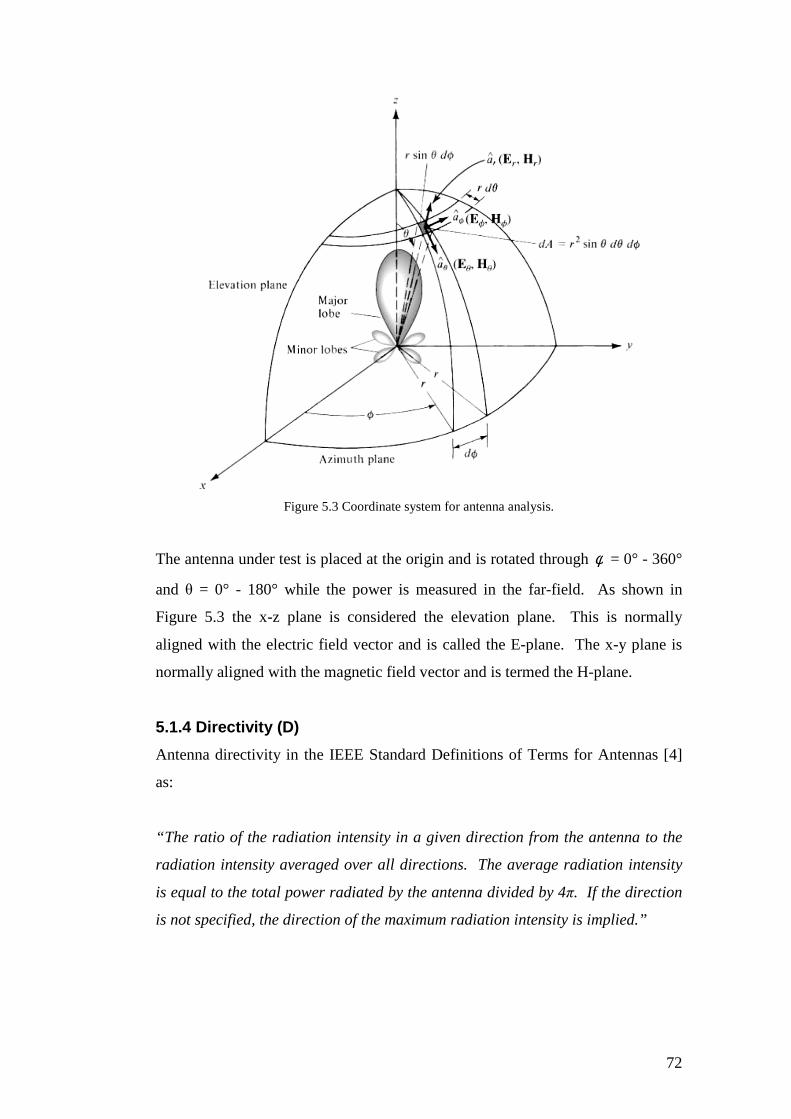
72
Figure 5.3 Coordinate system for antenna analysis.
The antenna under test is placed at the origin and is rotated through φ = 0° - 360°
and θ = 0° - 180° while the power is measured in the far-field. As shown in
Figure 5.3 the x-z plane is considered the elevation plane. This is normally
aligned with the electric field vector and is called the E-plane. The x-y plane is
normally aligned with the magnetic field vector and is termed the H-plane.
5.1.4 Directivity (D)
Antenna directivity in the IEEE Standard Definitions of Terms for Antennas [4]
as:
“The ratio of the radiation intensity in a given direction from the antenna to the
radiation intensity averaged over all directions. The average radiation intensity
is equal to the total power radiated by the antenna divided by 4π. If the direction
is not specified, the direction of the maximum radiation intensity is implied.”

73
Essentially, this means that the directivity of an antenna is the ratio of the
radiation intensity in a given direction over that of a isotropic source. This can be
written as:
radP
U
U
UD
π4
0
== (5.8)
Where, U = radiation intensity (W/unit solid angle)
U0 = radiation intensity of an isotropic source (W/unit solid angle)
Prad = total radiated power (W)
If the antenna was to radiate in all directions (isotropic radiator) then its
directivity would be unity. As an isotropic radiator cannot be realised practically,
the most comparable antenna is a short dipole, which has a directivity of 1.5.
Any other antenna will have a higher directivity than 1.5, which means their
patterns are more focused in a particular direction.
5.1.5 Antenna Efficiency (η)
Like other microwave components, antennas can suffer from losses. The total
antenna efficiency takes into account the losses at the input terminals, and within
the structure of the antenna itself.
The mismatch or reflection efficiency (ηr) is directly related to the return loss (Γ)
and can be defined as:
)1(2Γ−=rη (5.9)
The radiation efficiency (η) is a measure of how much power is lost in the antenna
due to conductor and dielectric losses. These losses reduce the radiation in any
given direction and can be expressed as:
in
rad
P
P=η (5.10)
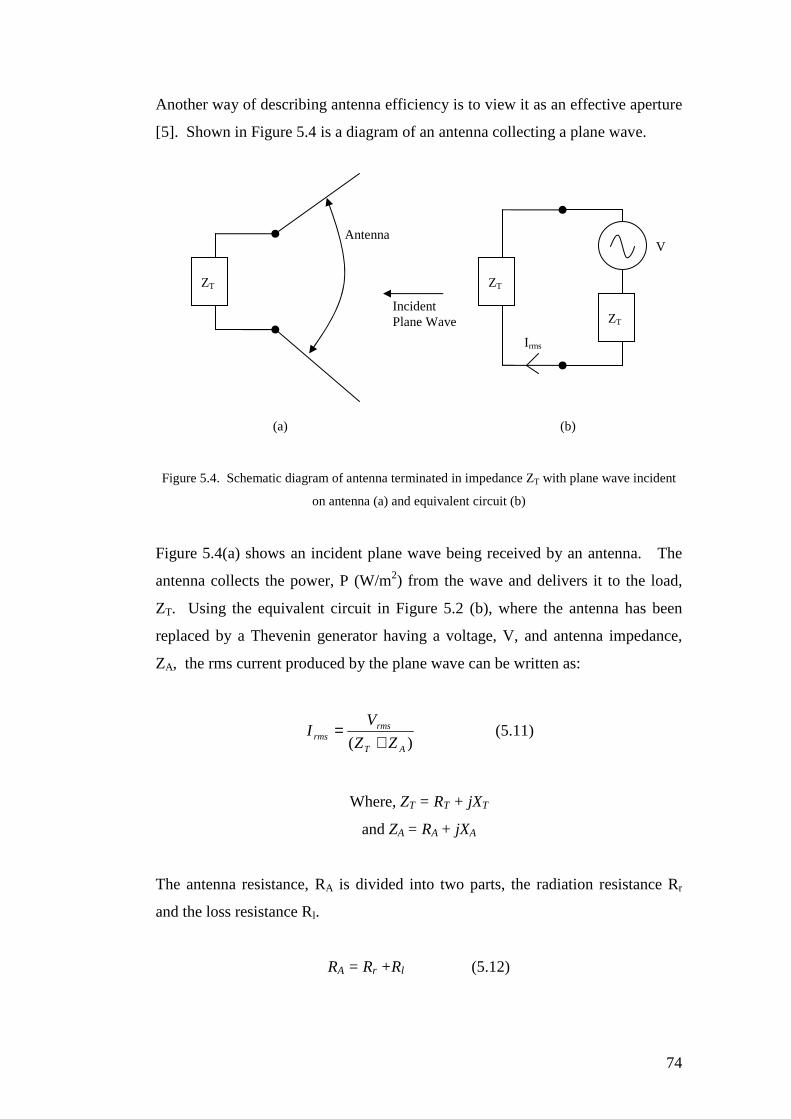
74
Another way of describing antenna efficiency is to view it as an effective aperture
[5]. Shown in Figure 5.4 is a diagram of an antenna collecting a plane wave.
Figure 5.4. Schematic diagram of antenna terminated in impedance ZT with plane wave incident
on antenna (a) and equivalent circuit (b)
Figure 5.4(a) shows an incident plane wave being received by an antenna. The
antenna collects the power, P (W/m2) from the wave and delivers it to the load,
ZT. Using the equivalent circuit in Figure 5.2 (b), where the antenna has been
replaced by a Thevenin generator having a voltage, V, and antenna impedance,
ZA, the rms current produced by the plane wave can be written as:
)( AT
rmsrms ZZ
VI
+= (5.11)
Where, ZT = RT + jXT
and ZA = RA + jXA
The antenna resistance, RA is divided into two parts, the radiation resistance Rr
and the loss resistance Rl.
RA = Rr +Rl (5.12)
Antenna
Incident Plane Wave
(a)
ZT ZT
ZT
V
Irms
(b)

75
The real power delivered to the load is then defined as:
W = Irms2RT (Watts) (5.13)
The ratio between the power (W) at the load, and the power density (P) of the
incident wave, is known as the effective aperture, Ae, and can be described as:
Ae = W/P (m2) (5.14)
As shown, the effective aperture takes into account any mismatch losses and
radiation losses, and can be thought of as the ‘capture area’ of the antenna. If
there are no losses due to mismatch or the antenna, then it can be seen, for a given
frequency, that if the antenna size is reduced, its efficiency is reduced. The limit
on the size reduction of antennas, and the consequent impact on efficiency will be
discussed in chapter 9.
5.1.6 Antenna Gain
Antenna gain, G, is the product of efficiency and directivity, and is defined in the
IEEE Standard Definitions of Terms for Antennas [6] as:
“The ratio of the intensity, in a given direction, to the radiation intensity that
would be obtained if the power accepted by the antenna were radiated
isotropically. The radiation intensity corresponding to the isotropically radiated
power is equal to the power accepted by the antenna divided by 4π”
This can be expressed as:
inP
UG
),(4 φθπ= (5.15)
Unless specified, it is assumed that the antenna is receiving a signal in the
direction of maximum gain. It is also common for the gain to be expressed in
decibels and referenced to an isotropic source (G = 1), as shown in Equation 5.16.
G (dBi) = 10 Log (G/1) (5.16)

76
5.1.7 Polarisation
The polarisation of an antenna refers to the orientation of the electric field vector
of the radiated wave and is defined in the IEEE Standard Definitions of Terms for
Antennas [7] as:
“The property of an electromagnetic wave describing the time-varying direction
and relative magnitude of the electric-field vector; specifically, the figure traced
as a function of time by the extremity of the vector at a fixed location in space,
and the sense in which it is traced, as observed along the direction of
propagation”
Polarisation is the curve traced by the tip of the electric field vector viewed in the
direction of propagation. Figure 5.5 shows a typical trace as a function of time
[8].
Figure 5.5. Rotation of a plane electromagnetic wave and its polarisation ellipse at
z = 0 as a function of time.

77
The polarisation of the wave may be linear, circular, or elliptical. The
instantaneous electric field of a plane wave, travelling in the negative z direction,
may be written as:
ytzExtzEtzE yx ˆ),(ˆ),(),( += (5.17)
The instantaneous components are related to their complex counterparts by:
Ex (z, t) = Ey cos (ωt + βz + θx) (5.18)
and
Ey (z, t) = Ex cos (ωt + βz + θy) (5.19)
Where Ex and Ey are the maximum magnitudes and θx and θy are the phase angles
of the x and y components respectively, ω is the angular frequency, and β is the
propagation constant.
For the wave to be linearly polarised, the phase difference between the two
components must be:
∆θ = θy – θx = nπ,
Where, n = 0, 1, 2, (5.20)
For the wave to be circularly polarised, the magnitudes of the two components
must be equal i.e. Ex = Ey, and the phase difference ∆θ is an odd multiple of π/2.
This is illustrated by Equation 5.21.
∆θ = θy – θx (5.21)
If Ex ∫ Ey or ∆θ does not satisfy (5.20) and (5.21), then the resulting polarisation
is elliptical, as shown in Figure 5.3. The performance of a circularly-polarised
antenna is characterised by its axial ratio (AR). The AR is defined as the ratio of
the major axis to the minor axis and is described below.

78
OB
OAAR ==
axisminor
axismajor (5.22)
For circular polarisation OA = OB (i.e. AR = 1), whereas for linear polarisation
AR → ¶. Typically, it is only possible to generate AR over a limited frequency
range. The 3dB bandwidth is used to define AR = 1 = 0dB at the operating
frequency.
Now that the fundamental parameters used to characterise an antennas
performance have been discussed the next stage is to investigate the simulation
software used, the fabrication process and the test apparatus used. This is
discussed in the next chapter.

79
6. Antenna design, fabrication and experimental analysis
The object of this chapter is to give an insight into the process involved in
designing, fabricating and experimentally verifying an antenna. The software
used to design antennas is discussed, along with the fabrication process and the
tools used to characterise the performance of antennas.
6.1 High Frequency Simulation Software (HFSS)
HFSS was used as an evaluation and design tool for the majority of the work
carried out in this thesis. Many papers have been published in the past, [1] and
more recently [2], verifying its accuracy. HFSS utilizes a 3D full-wave Finite
Element Method to compute the electrical behaviour of high-frequency and high-
speed components [3]. Models can be created with different materials,
boundaries and geometries. The basic mesh element used is a tetrahedron, which
allows the user to mesh any arbitrary 3D geometry, such as complex curves and
shapes. The mesh can be defined automatically by the solver, but quite often this
does not give satisfactory results and the user has to define mesh operations, such
as, seeding the mesh, maximum aspect ratio and curve surface approximations.
The next section discusses the process once a model has been subdivided into
elements.
6.1.1 Theoretical basis of HFSS
Once a mesh is created, basis functions are defined for each tetrahedra. The basis
functions, Wn,, define the conditions between the nodal locations in the overall
mesh of tetrahedral based on the problem inputs. The basis functions are then
multiplied by the field Equation, 6.1, derived from Maxwell’s equations.
01 2
0 =−
××∇ EkE r
r
rrε
µ (6.1)
The result is then integrated over the volume of the tetrahedron as shown by
Equation 6.2.

80
∫ =
−
××∇⋅
V rr
n dVEkEW 01 2
0
rrε
µ (6.2)
This is then rewritten using the Green’s and divergence theorems and is then set
equal to the excitation/boundary terms, as shown in Equation 6.3.
( )∫ ∫=
−
ו×∇
V Srr
n dVEkEWrr
εµ
20
1boundary term (6.3)
The electric-field vector is then written as a summation of unknowns; Xm,
multiplied by the same basis functions used in generating the initial series of
equations, and is shown by Equation 6.4.
∑=
=N
mmmWXE
1
r (6.4)
The resulting equations allow the solution of the unknowns, Xm, to find the
electric-fields. The general form of the expression is shown by Equation 6.5.
( ) ( )∑ ∫∫=
=
−
ו×∇⋅
N
m SV mnrm
rnm dStermsboundarydVWWkWWX
1
20
1 εµ
(6.5)
Once the values have been calculated using the solver, a second adaptive pass
occurs and HFSS compares the S-parameters to the previous mesh-based solution.
This process is repeated and the difference between the two solutions calculated.
This process is continued until the solution has converged to an acceptable
difference, usually 2% or less, this being defined by the user. Shown in Figure
6.1 is a structure subdivided into elements after several passes.
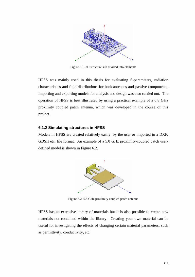
81
Figure 6.1. 3D structure sub divided into elements
HFSS was mainly used in this thesis for evaluating S-parameters, radiation
characteristics and field distributions for both antennas and passive components.
Importing and exporting models for analysis and design was also carried out. The
operation of HFSS is best illustrated by using a practical example of a 6.8 GHz
proximity coupled patch antenna, which was developed in the course of this
project.
6.1.2 Simulating structures in HFSS
Models in HFSS are created relatively easily, by the user or imported in a DXF,
GDSII etc. file format. An example of a 5.8 GHz proximity-coupled patch user-
defined model is shown in Figure 6.2.
Figure 6.2. 5.8 GHz proximity coupled patch antenna
HFSS has an extensive library of materials but it is also possible to create new
materials not contained within the library. Creating your own material can be
useful for investigating the effects of changing certain material parameters, such
as permittivity, conductivity, etc.

82
With the model created, the boundary conditions need to be specified. Generally,
these can be split into excitations or surface approximations. There are many
types of excitations possible in HFSS, but the main ones used for the models
throughout the thesis are either wave ports or lumped ports. Ports are a unique
type of boundary condition that allows energy to flow into and out of a structure.
• Wave ports – These ports can be placed internally or externally, and
support multiple modes of transmission. They also support reference
plane de-embedding and arbitrary mode re-normalisation. They are well
suited for exciting most transmission lines, though setting them up can be
complex.
• Lumped ports – These ports are recommended only for surfaces internal to
the geometric model. There is only a single mode excited at the port
(TEM) and there is no de-embedding. They are simpler to set up and are
ideal for exciting transmission lines such as microstrip.
Figure 6.3 shows an example of a wave-port being used to excite a co-axial mode.
The orientation of the field at the port can clearly be seen to be in a co-axial
mode.
Figure 6.3. Wave port excitation on a SMA connector
With the model created and a excitation specified, the next stage is to select the
surface approximation for the radiation boundary. There are two main options:
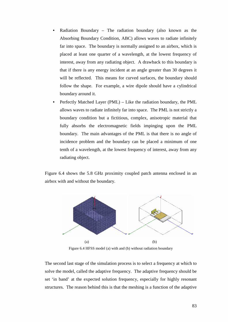
83
• Radiation Boundary – The radiation boundary (also known as the
Absorbing Boundary Condition, ABC) allows waves to radiate infinitely
far into space. The boundary is normally assigned to an airbox, which is
placed at least one quarter of a wavelength, at the lowest frequency of
interest, away from any radiating object. A drawback to this boundary is
that if there is any energy incident at an angle greater than 30 degrees it
will be reflected. This means for curved surfaces, the boundary should
follow the shape. For example, a wire dipole should have a cylindrical
boundary around it.
• Perfectly Matched Layer (PML) – Like the radiation boundary, the PML
allows waves to radiate infinitely far into space. The PML is not strictly a
boundary condition but a fictitious, complex, anisotropic material that
fully absorbs the electromagnetic fields impinging upon the PML
boundary. The main advantages of the PML is that there is no angle of
incidence problem and the boundary can be placed a minimum of one
tenth of a wavelength, at the lowest frequency of interest, away from any
radiating object.
Figure 6.4 shows the 5.8 GHz proximity coupled patch antenna enclosed in an
airbox with and without the boundary.
(a) (b)
Figure 6.4 HFSS model (a) with and (b) without radiation boundary
The second last stage of the simulation process is to select a frequency at which to
solve the model, called the adaptive frequency. The adaptive frequency should be
set ‘in band’ at the expected solution frequency, especially for highly resonant
structures. The reason behind this is that the meshing is a function of the adaptive

84
frequency i.e. higher frequency, larger mesh. It is a common misconception that
setting the adaptive frequency higher will give greater accuracy. If the adaptive
frequency is set higher than the operating frequency the resonance may be missed.
If a wideband structure is being analysed, then the frequency should be set at the
highest frequency of expected operation. After selecting the adaptive frequency,
the final stage is to choose the frequency sweep. When specifying the frequency
sweep there are three options.
• Discrete – This sweep offers the highest accuracy as it performs a full
solution at every frequency specified in the sweep. This sweep is best
when only a few frequency points are necessary to accurately represent the
results in a frequency range.
• Interpolative - Estimates a solution for an entire frequency range. This
sweep is best when the frequency range is wide and the frequency
response is smooth e.g. a filter.
• Fast - Generates a unique full-field solution for each division within a
frequency range. This sweep is best for models that will abruptly resonate
or change operation in the frequency band. A fast sweep will obtain an
accurate representation of the behaviour near the resonance.
Generally, either the discrete or fast sweep is used throughout this thesis.
As the model is simulated, it is important to observe the convergence of the
solution. For higher accuracy it is normal to specify at least three concurrent
convergent passes within the specified accuracy, normally 2% or less. This is
shown in Figure 6.5.
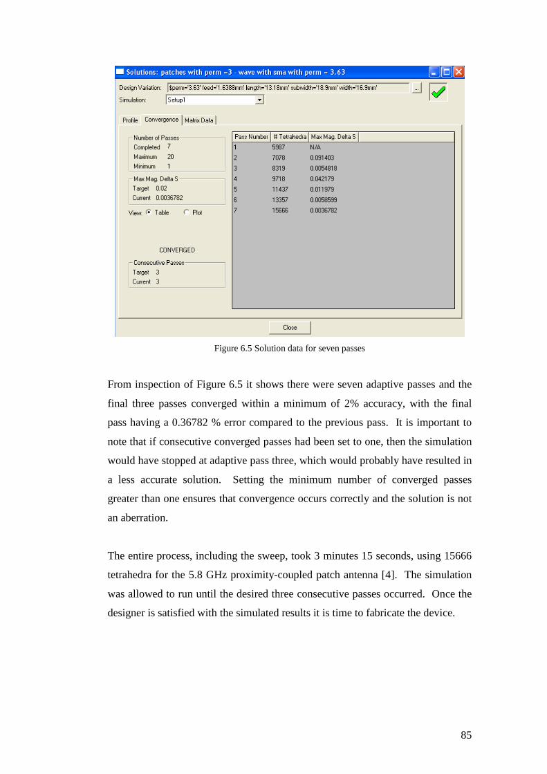
85
Figure 6.5 Solution data for seven passes
From inspection of Figure 6.5 it shows there were seven adaptive passes and the
final three passes converged within a minimum of 2% accuracy, with the final
pass having a 0.36782 % error compared to the previous pass. It is important to
note that if consecutive converged passes had been set to one, then the simulation
would have stopped at adaptive pass three, which would probably have resulted in
a less accurate solution. Setting the minimum number of converged passes
greater than one ensures that convergence occurs correctly and the solution is not
an aberration.
The entire process, including the sweep, took 3 minutes 15 seconds, using 15666
tetrahedra for the 5.8 GHz proximity-coupled patch antenna [4]. The simulation
was allowed to run until the desired three consecutive passes occurred. Once the
designer is satisfied with the simulated results it is time to fabricate the device.

86
6.3 Fabrication Processes
The fabrication of the antennas, investigated in this thesis, was carried out using
two technologies. The first is the standard PCB processing method, which
involves:
• Print mask
• Board with mask in place is exposed to light and developed
• Board is placed in a proprietary etch, which removes the copper that is not
protected by the exposed and developed resist
The resolution of the PCB process is limited, as the smallest gap that can be
obtained is between 250 µm and 300 µm.
The second process for fabrication of antennas in this thesis utilises the
technology available at the James Watt Nano-Fabrication Centre (JWNC). The
material used for the substrate is gallium arsenide (GaAs), a semiconductor used
to make devices such as Monolithic Microwave Integrated Circuits (MMIC’s),
infrared light-emitting diodes, laser diodes and solar cells. The antennas designed
in chapter nine were constructed using the following process:
• Submit design to beam writer
• Spin resist on wafer
• Pattern transferred to resist using electron beam lithography
• Metal deposited via metal evaporation, which leaves a 1.2µm Gold (Au)
on top of a 50nm Nickel Chromium (NiCr) layer
• Wafer is then treated by a solvent, which removes resist plus any metal not
attached to the substrate
The second process has a minimum feature size of 10nm.

87
6.4 Testing facilities
Throughout this thesis several testing apparatus were used. These include various
Vector Network Analysers (VNA), some with on-wafer probing capability, as
well as Spectrum Analysers and Communications Analysers. As there were many
different models of VNAs used, the models are specified in the relevant sections.
Antenna radiation patterns have been obtained for various antennas by using
either near- field or far-field systems. Towards the end of this project, Glasgow
University purchased a spherical near-field antenna measurement system. This is
now described.
6.4.1 Near-field anechoic chamber
The Near-field anechoic chamber at Glasgow University is a NSI-700S-90
spherical near-field measurement system (manufactured and installed by Near-
field Systems Inc (NSI)). This means that it can give near-complete 3D
characterisation of the antenna. The chamber works on the principle of measuring
the electromagnetic field distribution near the antenna and using Huygens
principle to compute the far-field response [5].
The chamber has a selection of Open Ended Waveguide Probes (OEWG) with
high frequency limit of 20 GHz, which are used for accurate measurement of
highly directional antennas. There is also a wideband (500MHz to 18 GHz) Dual
Polarised Log-Periodic antenna (DPLA), which can be used for any antenna but is
better suited to low-gain omni-directional antennas. The dual-polarisation also
allows for measurement of circular polarisation and cross-polarisation levels.
Figure 6.6 shows a simple diagram layout of the chamber with the measurement
coordinates.
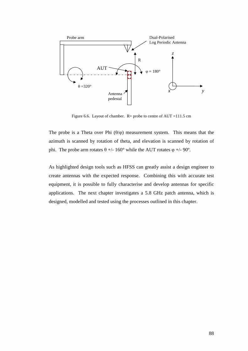
88
Figure 6.6. Layout of chamber. R= probe to centre of AUT =111.5 cm
The probe is a Theta over Phi (θ/φ) measurement system. This means that the
azimuth is scanned by rotation of theta, and elevation is scanned by rotation of
phi. The probe arm rotates θ +/- 160° while the AUT rotates φ +/- 90º.
As highlighted design tools such as HFSS can greatly assist a design engineer to
create antennas with the expected response. Combining this with accurate test
equipment, it is possible to fully characterise and develop antennas for specific
applications. The next chapter investigates a 5.8 GHz patch antenna, which is
designed, modelled and tested using the processes outlined in this chapter.
φ = 180°
θ =320°
Probe arm
AUT
y
z
x
Dual-Polarised Log Periodic Antenna
R
Antenna pedestal
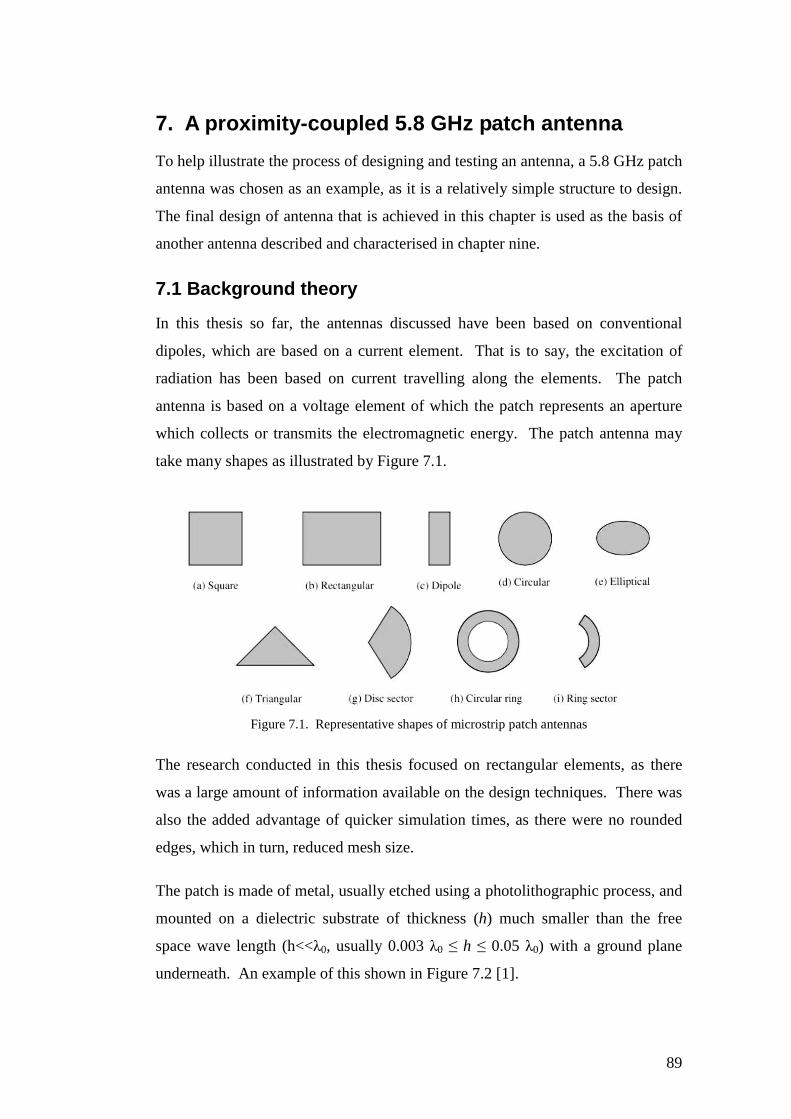
89
7. A proximity-coupled 5.8 GHz patch antenna
To help illustrate the process of designing and testing an antenna, a 5.8 GHz patch
antenna was chosen as an example, as it is a relatively simple structure to design.
The final design of antenna that is achieved in this chapter is used as the basis of
another antenna described and characterised in chapter nine.
7.1 Background theory
In this thesis so far, the antennas discussed have been based on conventional
dipoles, which are based on a current element. That is to say, the excitation of
radiation has been based on current travelling along the elements. The patch
antenna is based on a voltage element of which the patch represents an aperture
which collects or transmits the electromagnetic energy. The patch antenna may
take many shapes as illustrated by Figure 7.1.
Figure 7.1. Representative shapes of microstrip patch antennas
The research conducted in this thesis focused on rectangular elements, as there
was a large amount of information available on the design techniques. There was
also the added advantage of quicker simulation times, as there were no rounded
edges, which in turn, reduced mesh size.
The patch is made of metal, usually etched using a photolithographic process, and
mounted on a dielectric substrate of thickness (h) much smaller than the free
space wave length (h<<λ0, usually 0.003 λ0 ≤ h ≤ 0.05 λ0) with a ground plane
underneath. An example of this shown in Figure 7.2 [1].
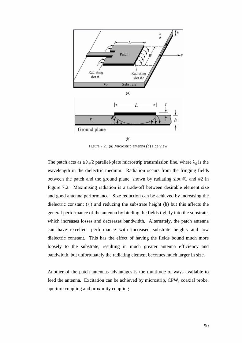
90
(a)
(b)
Figure 7.2. (a) Microstrip antenna (b) side view
The patch acts as a λg/2 parallel-plate microstrip transmission line, where λg is the
wavelength in the dielectric medium. Radiation occurs from the fringing fields
between the patch and the ground plane, shown by radiating slot #1 and #2 in
Figure 7.2. Maximising radiation is a trade-off between desirable element size
and good antenna performance. Size reduction can be achieved by increasing the
dielectric constant (εr) and reducing the substrate height (h) but this affects the
general performance of the antenna by binding the fields tightly into the substrate,
which increases losses and decreases bandwidth. Alternately, the patch antenna
can have excellent performance with increased substrate heights and low
dielectric constant. This has the effect of having the fields bound much more
loosely to the substrate, resulting in much greater antenna efficiency and
bandwidth, but unfortunately the radiating element becomes much larger in size.
Another of the patch antennas advantages is the multitude of ways available to
feed the antenna. Excitation can be achieved by microstrip, CPW, coaxial probe,
aperture coupling and proximity coupling.

91
7.2 Design of Patch antenna - The transmission line model
There are many methods of analysis used with patch antennas. One of the most
popular is the transmission line model, which is based on equivalent magnetic
current distribution around the patch edges. The patch is viewed as a transmission
line resonator with no transverse field variations i.e. the field only varies along the
length, and the radiation occurs from the fringing fields, which are viewed as
open circuits at the ends of the transmission line. The patch is then represented as
two slots spaced by the length of the patch. The transmission line model cannot
be used for all shapes of patch and is not the most accurate, but it is very quick
and easy to use, especially when used in conjunction with a finite element solver
such as HFSS.
The fundamental mode of a patch antenna is the TM01 mode. The subscript
depicts the orientation i.e. along the y-axis of the two radiating slots, or voltage
maximums, as shown in Figure 7.2. To excite the TM01 mode, the length, L,
should be slightly less than λg/2, where λg is defined by:
re
g ελλ 0= (7.1)
Where, εre is the effective dielectric constant in the medium. This value accounts
for the fact that not all the fringing fields are bound inside the substrate. The
effective dielectric constant is less than the dielectric constant and is given by [2]:
2/1
1212
1
2
1−
+−++=W
hrrre
εεε (7.2)
Where, W is the width of the patch.
Equation 7.2 omits the fact that the effective dielectric constant is frequency
dependant. As frequency increases, the fields occupy more of the substrate and
the value of effective dielectric constant moves towards the value of dielectric
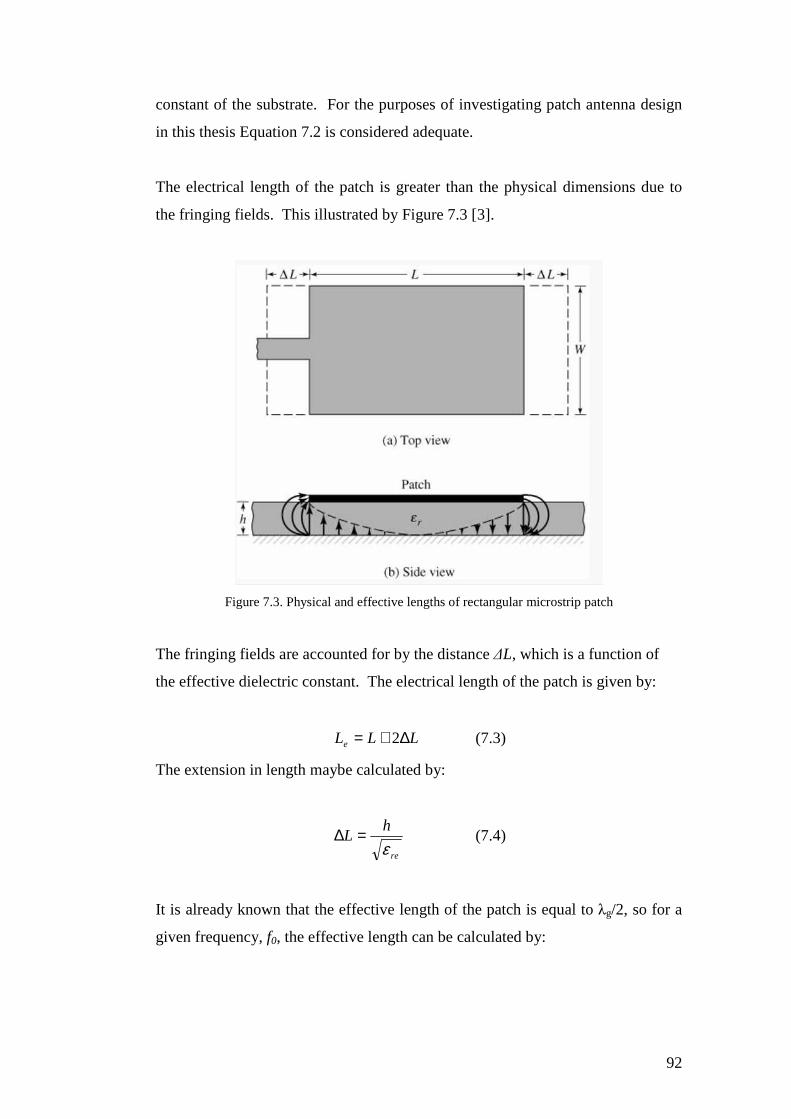
92
constant of the substrate. For the purposes of investigating patch antenna design
in this thesis Equation 7.2 is considered adequate.
The electrical length of the patch is greater than the physical dimensions due to
the fringing fields. This illustrated by Figure 7.3 [3].
Figure 7.3. Physical and effective lengths of rectangular microstrip patch
The fringing fields are accounted for by the distance ∆L, which is a function of
the effective dielectric constant. The electrical length of the patch is given by:
LLLe ∆+= 2 (7.3)
The extension in length maybe calculated by:
re
hL
ε=∆ (7.4)
It is already known that the effective length of the patch is equal to λg/2, so for a
given frequency, f0, the effective length can be calculated by:
93
rere
ef
cLLL
εελ
0
0
222 ==∆+= (7.5)
Where, c = velocity of light in free space = 3 x 10⁸ m/s. To obtain the resonant
frequency for any TMmn mode the following expression can be used [4]:
2/122
02
+
=W
n
L
mcf
rε (7.6)
To calculate the effective dielectric constant using Equation 7.6, W must be
known. W is taken as being equal to a half-wavelength corresponding to the
average of the two dielectric mediums i.e. substrate and air.
2
12 0
+=
rf
cW
ε (7.7)
The value obtained for W by using Equation 7.7 can be increased or decreased. If
it is increased then both bandwidth and directivity are increased due to the larger
aperture area. If W is further increased then higher order modes will be excited.
Decreasing W has the opposite effect on bandwidth and directivity but is
sometimes advantageous, particularly when trying to excite circular polarisation.
The design procedure for obtaining physical dimensions of the patch antenna is as
follows:
• Specify operating frequency (f0) and substrate (εr)
• Calculate width (W)
• Calculate effective permittivity (reε )
• Calculate physical length (L)
The radiation patterns for the fundamental TM01 mode are given by Kumar [5]
and are based on the combination of two radiating slots of width We and length
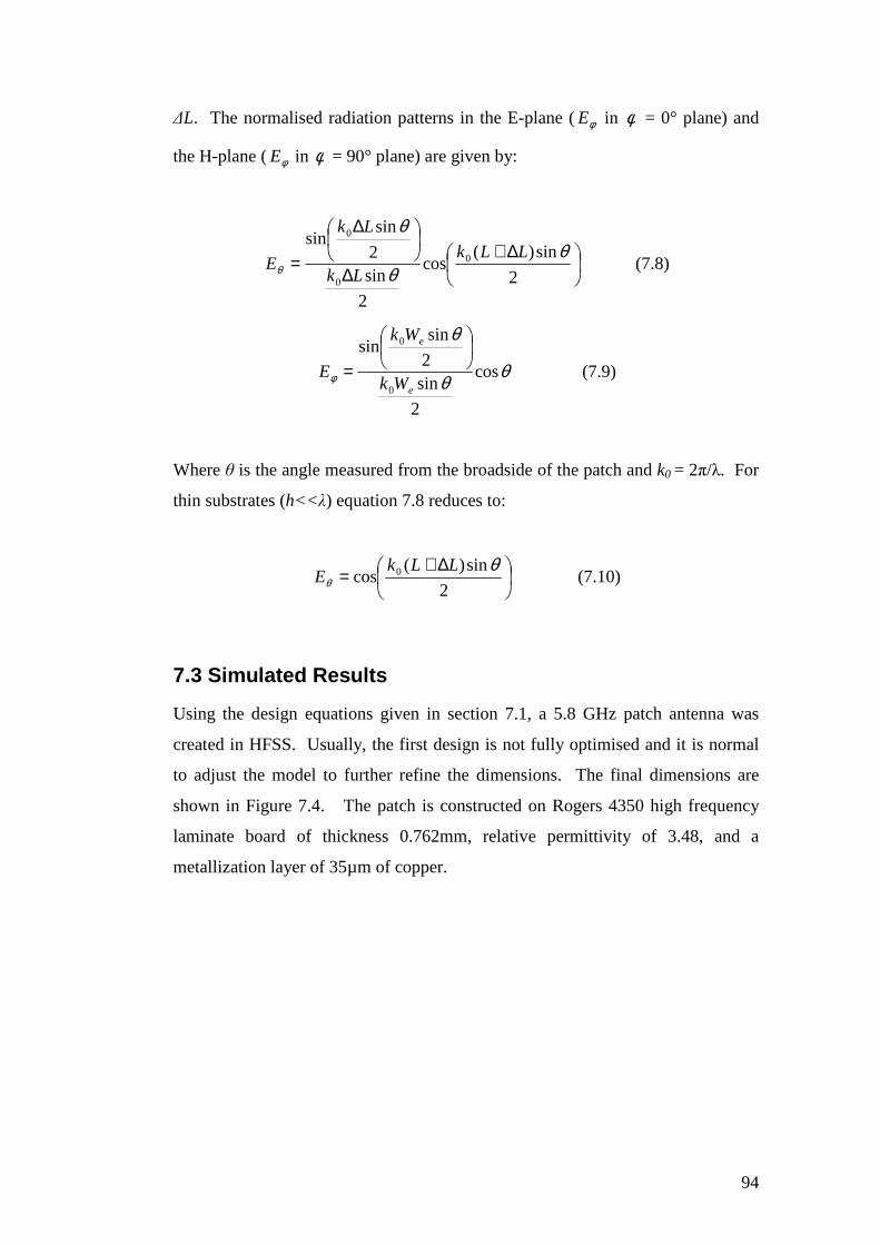
94
∆L. The normalised radiation patterns in the E-plane ( φE in φ = 0° plane) and
the H-plane ( φE in φ = 90° plane) are given by:
∆+∆
∆
=2
sin)(cos
2
sin2
sinsin
0
0
0
θθ
θ
θLLk
Lk
Lk
E (7.8)
θθ
θ
φ cos
2
sin2
sinsin
0
0
e
e
Wk
Wk
E
= (7.9)
Where θ is the angle measured from the broadside of the patch and k0 = 2π/λ. For
thin substrates (h<< λ) equation 7.8 reduces to:
∆+=
2
sin)(cos 0 θ
θLLk
E (7.10)
7.3 Simulated Results
Using the design equations given in section 7.1, a 5.8 GHz patch antenna was
created in HFSS. Usually, the first design is not fully optimised and it is normal
to adjust the model to further refine the dimensions. The final dimensions are
shown in Figure 7.4. The patch is constructed on Rogers 4350 high frequency
laminate board of thickness 0.762mm, relative permittivity of 3.48, and a
metallization layer of 35µm of copper.

95
L W Lsub Wsub
13.225 mm 16.9 mm 40 mm 19 mm
Figure 7.4. HFSS model of 5.8 GHz patch antenna with final dimensions
The simulated results for S11 and the 3D E-field are shown in Figure 7.5.
Lsub
Wsub
W L

96
(a)
(b)
Figure 7.5 Simulated results for (a) S11 and (b) 3D E-field
7.4 Testing antenna and redesign
Once the antenna has been fabricated two main investigations are carried out, S-
parameters and radiation pattern measurement. The S-parameters were measured
using an Agilent Vector Network Analyser (VNA). Figure 7.6 shows simulated
and experimental results for the 5.8 GHz patch antenna.
S11Mag (dB)
97
Figure 7.6. Simulated (blue) and experimental (red) results for S11
Inspection of Figure 7.6 shows that both the simulated and experimental results
are in agreement about the frequency of operation. However, there is quite a large
discrepancy between the values of magnitude for S11. When designing antennas,
the performance of the experimental results can differ from the simulated results.
This can usually be attributed to factors, such as design equation error, improper
use of simulation tools, fabrication and test equipment error and interference from
feed cables. If the frequency of design is greater than a few GHz then these errors
become pronounced. As the simulation in the previous section did not take
account of the test-cables, a model was created with a 10cm SMA cable attached
to it. This is shown in Figure 7.7.
Figure 7.7. 5.8 GHz patch antenna with 10 cm SMA cable
98
Using HFSS it is possible to view the fields to allow for a full understanding of
the operation of the antenna and cable. Figure 7.8 shows the surface current
present on the cable and antenna.
(a)
(b)
Figure 7.8. Surface current on 5.8 GHz patch antenna with 10 cm SMA cable
Inspection of the surface current revealed an interaction with the test cable.
Analysis of the 3D E-field, shown in Figure 7.8 (b), reveals the impact that the
test cable has on the radiation pattern. However, the simulated and experimental
results for S11 are in much better agreement and are shown in Figure 7.9. This
verifies the impact of the test-cable.
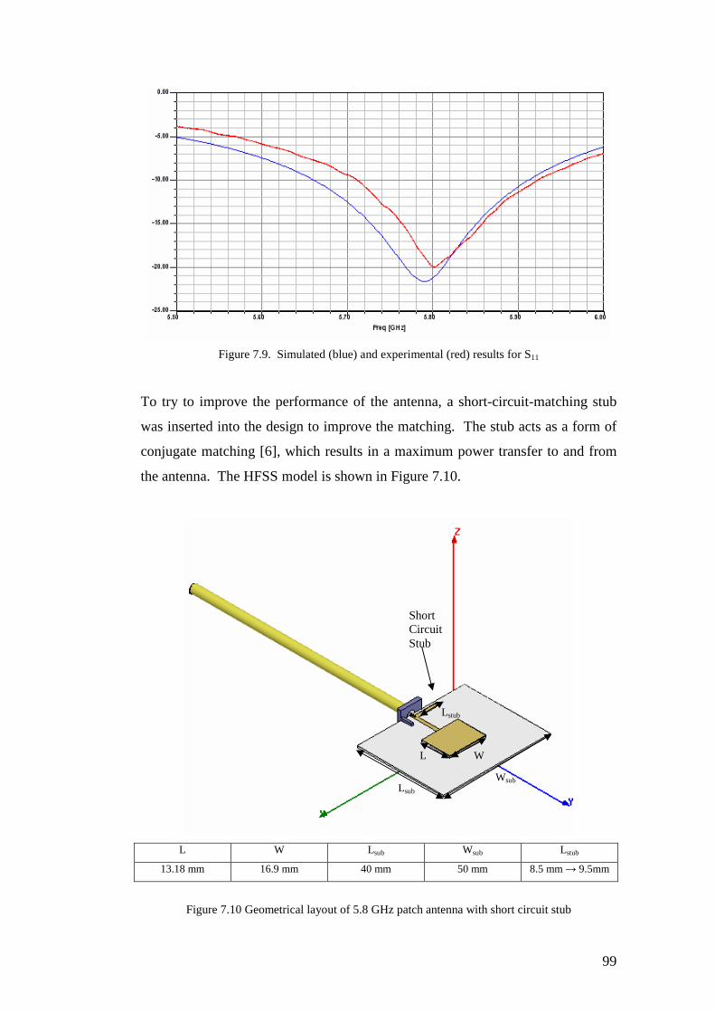
99
Figure 7.9. Simulated (blue) and experimental (red) results for S11
To try to improve the performance of the antenna, a short-circuit-matching stub
was inserted into the design to improve the matching. The stub acts as a form of
conjugate matching [6], which results in a maximum power transfer to and from
the antenna. The HFSS model is shown in Figure 7.10.
L W Lsub Wsub Lstub
13.18 mm 16.9 mm 40 mm 50 mm 8.5 mm → 9.5mm
Figure 7.10 Geometrical layout of 5.8 GHz patch antenna with short circuit stub
Short Circuit Stub
Lsub Wsub
L
Lstub
W
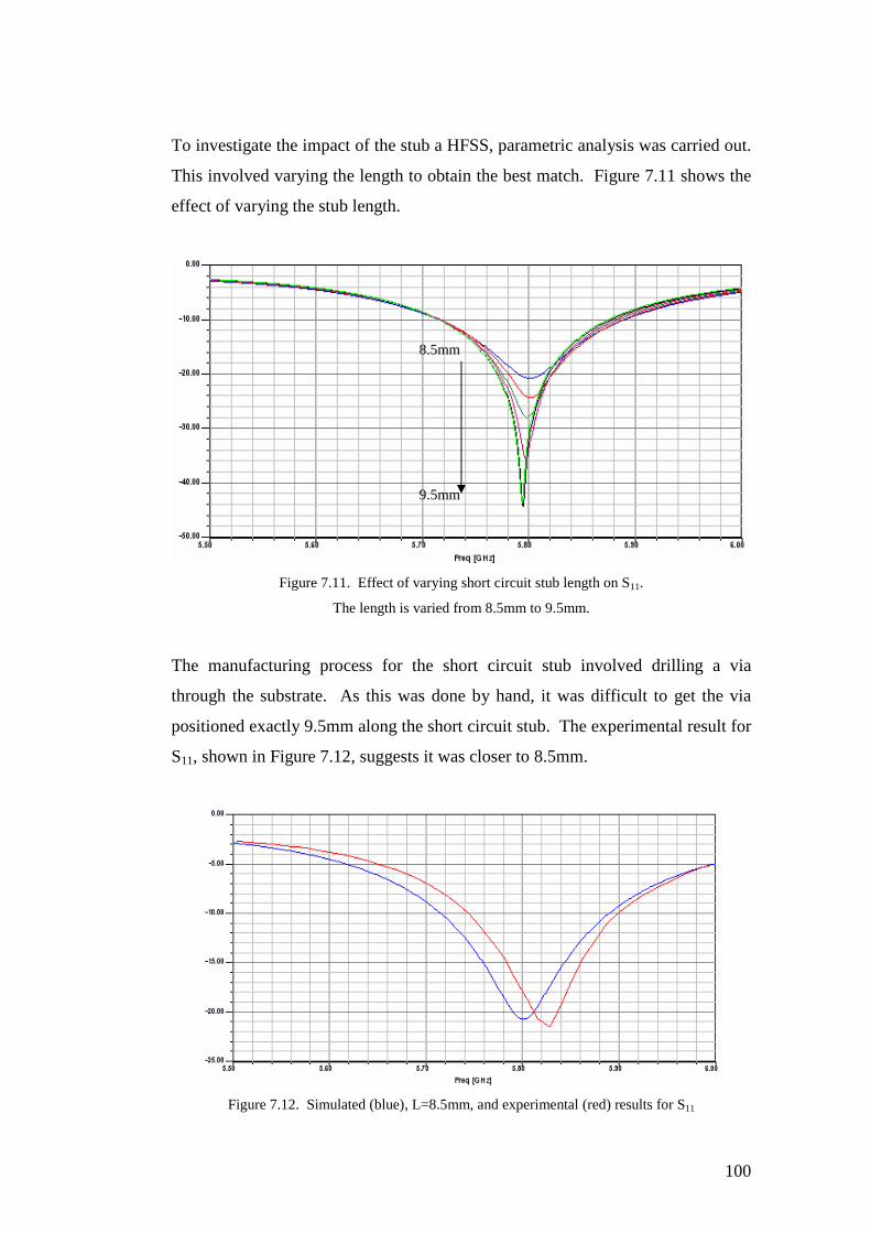
100
To investigate the impact of the stub a HFSS, parametric analysis was carried out.
This involved varying the length to obtain the best match. Figure 7.11 shows the
effect of varying the stub length.
Figure 7.11. Effect of varying short circuit stub length on S11.
The length is varied from 8.5mm to 9.5mm.
The manufacturing process for the short circuit stub involved drilling a via
through the substrate. As this was done by hand, it was difficult to get the via
positioned exactly 9.5mm along the short circuit stub. The experimental result for
S11, shown in Figure 7.12, suggests it was closer to 8.5mm.
Figure 7.12. Simulated (blue), L=8.5mm, and experimental (red) results for S11
8.5mm
9.5mm
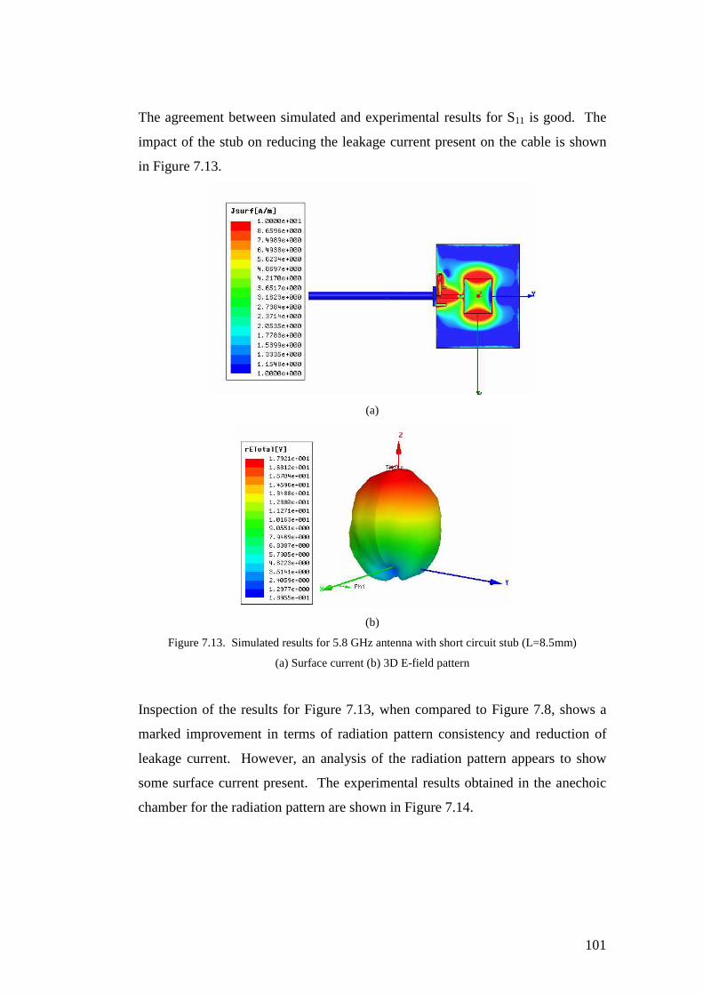
101
The agreement between simulated and experimental results for S11 is good. The
impact of the stub on reducing the leakage current present on the cable is shown
in Figure 7.13.
(a)
(b)
Figure 7.13. Simulated results for 5.8 GHz antenna with short circuit stub (L=8.5mm)
(a) Surface current (b) 3D E-field pattern
Inspection of the results for Figure 7.13, when compared to Figure 7.8, shows a
marked improvement in terms of radiation pattern consistency and reduction of
leakage current. However, an analysis of the radiation pattern appears to show
some surface current present. The experimental results obtained in the anechoic
chamber for the radiation pattern are shown in Figure 7.14.

102
Theta (degrees)
(a)
Phi (degrees)
(b)
Figure 7.14. Experimental radiation plots (a) horizontal cuts; red = principle cut; blue = simulated
(b) vertical cuts; red = principle cut; blue = simulated
The plots obtained are from the near-field data. The data obtained for the far-
field, which is obtained via a Fourier transform, was extremely noisy. As the
apparatus had been commissioned just before the end of the research discussed in
200 150 100 50 0 50 100 150 20040
30
20
10
0
⟩
25
⟨ ⟩ ⟨ ⟩
100 50 0 50 10035
30
25
20
15
10
5
phi1⟨ ⟩
25−
vcut12⟨ ⟩
phi0⟨ ⟩
vcut11⟨ ⟩,
E-field (V(dB))
E-field (V(dB))

103
this thesis, and a full familiarity was not obtained, the exact cause of the distortion
is unknown.
Inspection of the plots displayed in Figure 7.14 (a) show excellent agreement
between the simulated and experimental values for the principal cut. The plots in
Figure 7.14 (b) are not in such close agreement as those shown in Figure 7.14 (a)
but still show a drop in signal level at φ = 0°. Although the near-field data is
used to analyse the fields generated by the antenna, the plots in Figure 7.14
demonstrate that the near-field data, from the anechoic chamber, can be used to
extract useful data.
HFSS, combined with an awareness of the limitations of the manufacturing
process, the test equipment and interaction with surrounding bodies such as
cables, can accurately model 3D electromagnetic structures. Armed with this
knowledge of the difficulties associated with the simulation, antennas can be
modelled. The following chapters will now present the work carried out into the
research of various antenna structures for wireless sensor networks.

104
8. Ultra-Wide Band (UWB) Antennas
The overall aim of this chapter is to discuss Ultra-wideband architectures, the key
requirements for the Speckled Computing Consortium with respect to UWB, and
the UWB antennas designed, manufactured and tested during this project.
UWB antennas can be split into two classes, large and directional, and small and
omni-directional. An example of each is discussed. Typical performance
indicators such as return loss, radiation patterns and impulse response will also be
discussed.
8.1 UWB Architecture
UWB is defined as any radio technology that occupies greater than 500 MHz of
bandwidth, or greater than 25% of the operating centre frequency. In contrast,
most narrowband systems occupy a bandwidth of less than 10% of their operating
frequency. UWB radio is the term used to describe a technology that is also
known as "carrier-free", or "impulse radio". The basic concept of UWB radio is
to transmit and receive an extremely short duration burst of radio frequency (RF)
energy – typically a few tenths of picoseconds to a few nanoseconds in duration.
The advantage of this approach, compared to conventional narrowband systems,
is that the signal is transmitted over a very large frequency range (i.e. very short
pulse) and a signal with a very low spectral density can be received. The
difference of this technology over conventional narrowband systems is illustrated
in Figure 8.1.

105
Figure 8.1 Comparison of (a) Narrowband and (b) UWB architectures.
UWB removes the complex up-converting and down-converting stages of
narrowband radio, as shown by Figure 8.1. In effect, it simplifies the architecture,
which should result in lower power consumption. Other advantages of the UWB
approach are its potential to offer secure communications, resistance to multi-path
and high data rates [1]. A modulation scheme that can be used for UWB is pulse
position modulation (PPM) [2]. PPM is achieved by varying the position of a
pulse in time and/or its polarity. The following section looks at some important
requirements and some key performance indicators of UWB antennas.
8.2 Key requirements for UWB antennas
The key requirements that should be considered are as follows:
1. All of the parameters described in Chapter 4 i.e. pattern, gain efficiency etc.
must be considered when designing any type of antenna that is part of a RF-front
end. However, UWB antennas have additional design challenges. For example,
as the name suggests, the antenna must operate over a large bandwidth when
compared to narrowband antennas. The bandwidth is specified by both the
Federal Communications Commission (FCC) and the Office of Communications
(OFCOM) as 3.1 to 10.6 GHz; hence the antenna must achieve an impedance
bandwidth of 7.5 GHz.

106
2. Another important requirement is group delay. Group delay is defined as the
rate of change of the total phase shift, θ, with respect to the angular frequency, ω,
as shown in Equation 8.1.
)(
)( delay Group
ωθ
d
d= (8.1)
If the phase is linear throughout the bandwidth then the group delay is constant
throughout the bandwidth. Group delay can then be used as an indicator to show
how well a pulse will be transmitted with consideration of distortion and
dispersion. Normally, group delay is not considered in narrowband antenna
design because linear phase is normally quite easy to achieve over a narrow band.
Generally, if the group delay is in the tens of nano-seconds range, or less the
performance is acceptable [3] [4].
3. The radiation pattern is an extremely important requirement for UWB
antennas. For wireless sensor network applications, it is desirable to have an
omni-directional pattern so orientation of the transmitter/receiver is not as
important. As the antenna operates over a large bandwidth, its pattern at the low
frequency cut-off (3.1 GHz) is different to that of the pattern at the higher
frequency end (10.6 GHz), although good design can minimise this effect.
4. There are several other key requirements that are desirable for UWB antennas
and are summarised below:
• Compactness – Size is critical in terms of cost, as well as achieving the
ultimate aim of 5mm3 for this project.
• Planar – Ease of integration into monolithic circuits.
• Good VSWR (<2) – This is required across the whole band of operation so as
to maintain good matching and efficient operation.
• Constant Gain – This is desirable across the whole band of operation because
the signal is transmitted instantaneously across the whole (or a large part) of the
frequency band (3.1 – 10.6 GHz).

107
8.3 Initial designs of UWB Antennas
The theory and design of UWB antennas is not as well established as narrowband
antennas. However, many designs that have been validated by experimentation
and the results published [5]. Their performance has been evaluated for pulse
transmission and reception, as well as return loss, group delay and radiation
pattern. Two types of antenna, the Vivaldi [6] and a coplanar waveguide (CPW)-
fed monopole [7] were evaluated using a test-system developed at Glasgow in the
first year of the project and were published [8]. This evaluation was carried out as
follows.
8.3.1 UWB test system
The test system was used for investigating modulation formats, channel
characteristics, as well as the performance of the antennas in sending and
receiving pulses. The test system developed used bench equipment and readily
available materials. It consisted of a Tektronix CSA8000 sampling oscilloscope,
a Pulse Labs 4015C pulse generator with a 4015 pulse head, an impulse-forming
network (IFN 5208) and two broadband antennas for sending and receiving
pulses. The basic block diagram of the test system is given in Figure 8.2.
(a)
Figure 8.2 Basic block diagram of the test system.
Shown in Figure 8.3 is the signal before it is propagated through the antennas
under test, which are in a back-to-back configuration.
108
(a) (b)
Figure 8.3 (a) Output waveform from 4015C pulser with 10x attenuation (b) Output waveform
after the impulse forming network stage.
Return Loss measurements of the various UWB antennas were measured using a
HP8510 Vector Network Analyser (VNA).
8.3.2 The Vivaldi Antenna
The Vivaldi antenna was first described and characterised in 1979 by Gibson [6].
It is a wideband antenna that has been used extensively in radar applications as
part of arrays and ground penetrating applications [9]. More recently, the Vivaldi
antenna has been identified as being suitable for UWB communications [10].
With increasing interest in UWB as a viable radio architecture, the Vivaldi
antenna has attracted interest due to its theoretically infinite bandwidth. It is a
directional antenna with an end-fire characteristic.
The Vivaldi antenna designed in this project was constructed on a copper-clad
duroid substrate with a permittivity (εr) of 3.48 and a substrate thickness of 1.524
mm. The antenna was designed and verified by simulation using HFSS. A
schematic diagram of the antenna is shown in Figure 8.4.
50ps

109
(a)
(b)
L W Wback Ltaper Wslot
292.1mm 203.2 mm 150 mm 96.32 mm 93.75 mm
Figure 8.4. (a) Schematic of Vivaldi antenna designed in this project schematic. Length =
292.1mm, Width = 203.2 mm. (b) Magnified view of transition
As the radiating element of the Vivaldi antenna is a balanced structure, it was
important to create a balun to provide a match between the 50Ω co-axial input and
the antenna. The balun consists of a 50Ω microstrip to parallel plate transmission
line, which tapers into a slotline configuration, which then feeds the radiating
element. Figure 3.4 from chapter 3 shows the manipulation of the fields in the
balun.
Transmission line
Transition region
W
Wback
Wslot
Ltaper
L
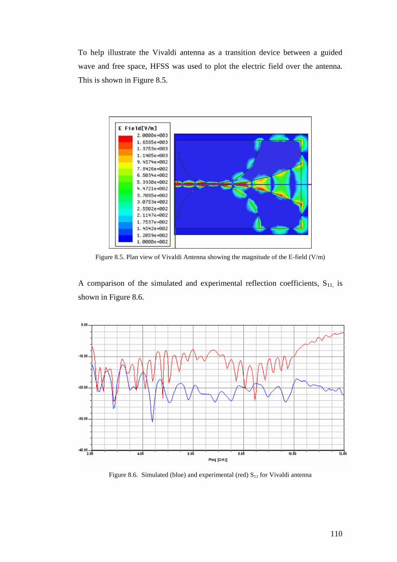
110
To help illustrate the Vivaldi antenna as a transition device between a guided
wave and free space, HFSS was used to plot the electric field over the antenna.
This is shown in Figure 8.5.
Figure 8.5. Plan view of Vivaldi Antenna showing the magnitude of the E-field (V/m)
A comparison of the simulated and experimental reflection coefficients, S11, is
shown in Figure 8.6.
Figure 8.6. Simulated (blue) and experimental (red) S11 for Vivaldi antenna
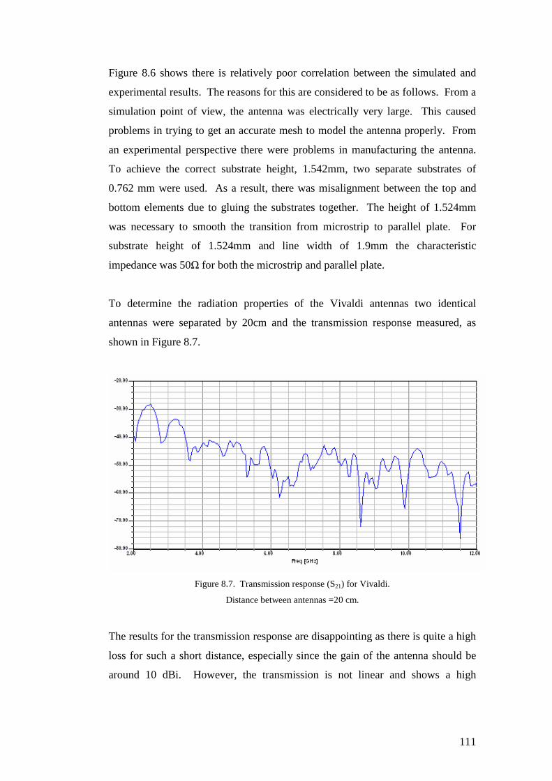
111
Figure 8.6 shows there is relatively poor correlation between the simulated and
experimental results. The reasons for this are considered to be as follows. From a
simulation point of view, the antenna was electrically very large. This caused
problems in trying to get an accurate mesh to model the antenna properly. From
an experimental perspective there were problems in manufacturing the antenna.
To achieve the correct substrate height, 1.542mm, two separate substrates of
0.762 mm were used. As a result, there was misalignment between the top and
bottom elements due to gluing the substrates together. The height of 1.524mm
was necessary to smooth the transition from microstrip to parallel plate. For
substrate height of 1.524mm and line width of 1.9mm the characteristic
impedance was 50Ω for both the microstrip and parallel plate.
To determine the radiation properties of the Vivaldi antennas two identical
antennas were separated by 20cm and the transmission response measured, as
shown in Figure 8.7.
Figure 8.7. Transmission response (S21) for Vivaldi.
Distance between antennas =20 cm.
The results for the transmission response are disappointing as there is quite a high
loss for such a short distance, especially since the gain of the antenna should be
around 10 dBi. However, the transmission is not linear and shows a high
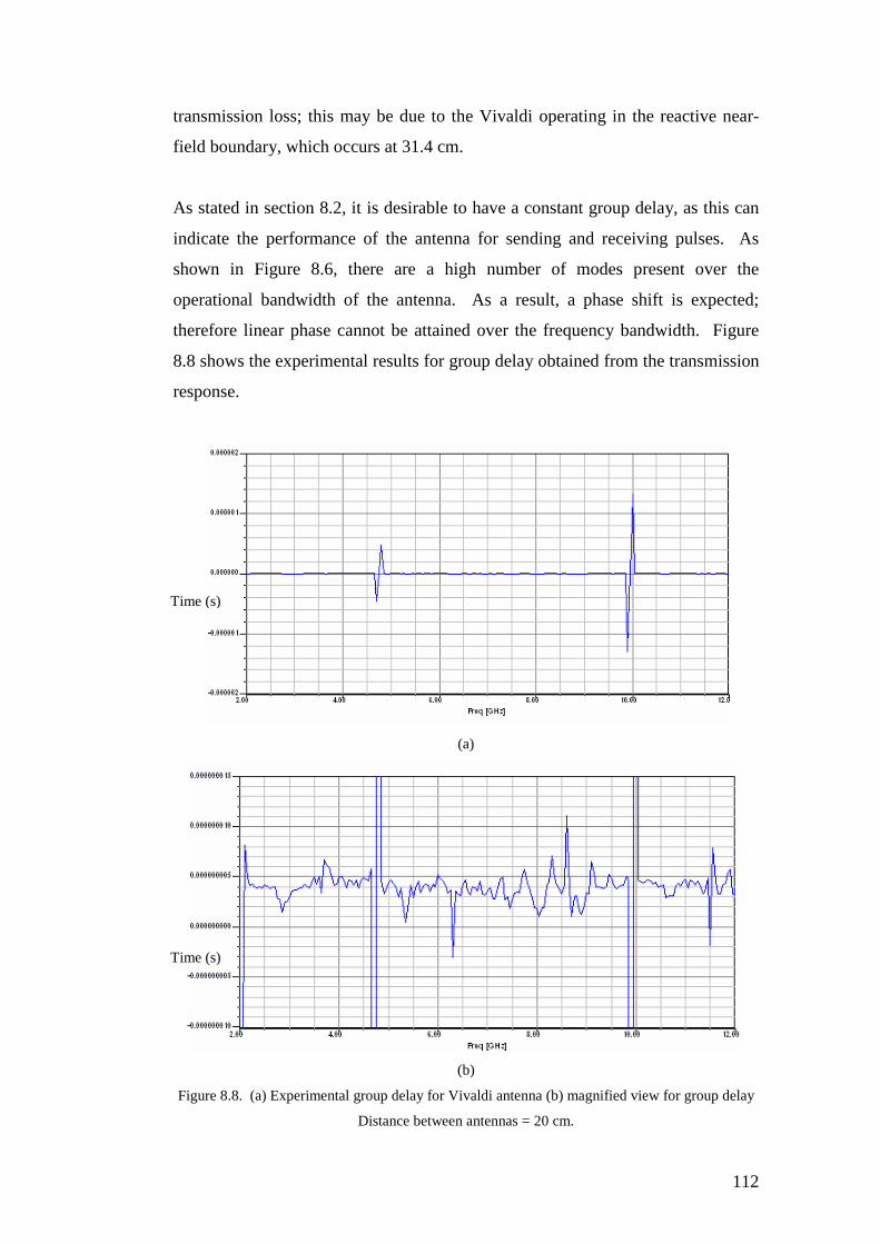
112
transmission loss; this may be due to the Vivaldi operating in the reactive near-
field boundary, which occurs at 31.4 cm.
As stated in section 8.2, it is desirable to have a constant group delay, as this can
indicate the performance of the antenna for sending and receiving pulses. As
shown in Figure 8.6, there are a high number of modes present over the
operational bandwidth of the antenna. As a result, a phase shift is expected;
therefore linear phase cannot be attained over the frequency bandwidth. Figure
8.8 shows the experimental results for group delay obtained from the transmission
response.
(a)
(b)
Figure 8.8. (a) Experimental group delay for Vivaldi antenna (b) magnified view for group delay
Distance between antennas = 20 cm.
Time (s)
Time (s)
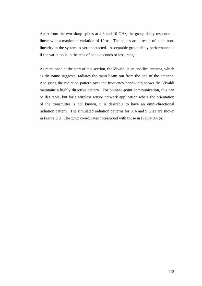
113
Apart from the two sharp spikes at 4.8 and 10 GHz, the group delay response is
linear with a maximum variation of 10 ns. The spikes are a result of some non-
linearity in the system as yet undetected. Acceptable group delay performance is
if the variation is in the tens of nano-seconds or less, range.
As mentioned at the start of this section, the Vivaldi is an end-fire antenna, which
as the name suggests, radiates the main beam out from the end of the antenna.
Analysing the radiation pattern over the frequency bandwidth shows the Vivaldi
maintains a highly directive pattern. For point-to-point communication, this can
be desirable, but for a wireless sensor network application where the orientation
of the transmitter is not known, it is desirable to have an omni-directional
radiation pattern. The simulated radiation patterns for 3, 6 and 9 GHz are shown
in Figure 8.9. The x,y,z coordinates correspond with those in Figure 8.4 (a).
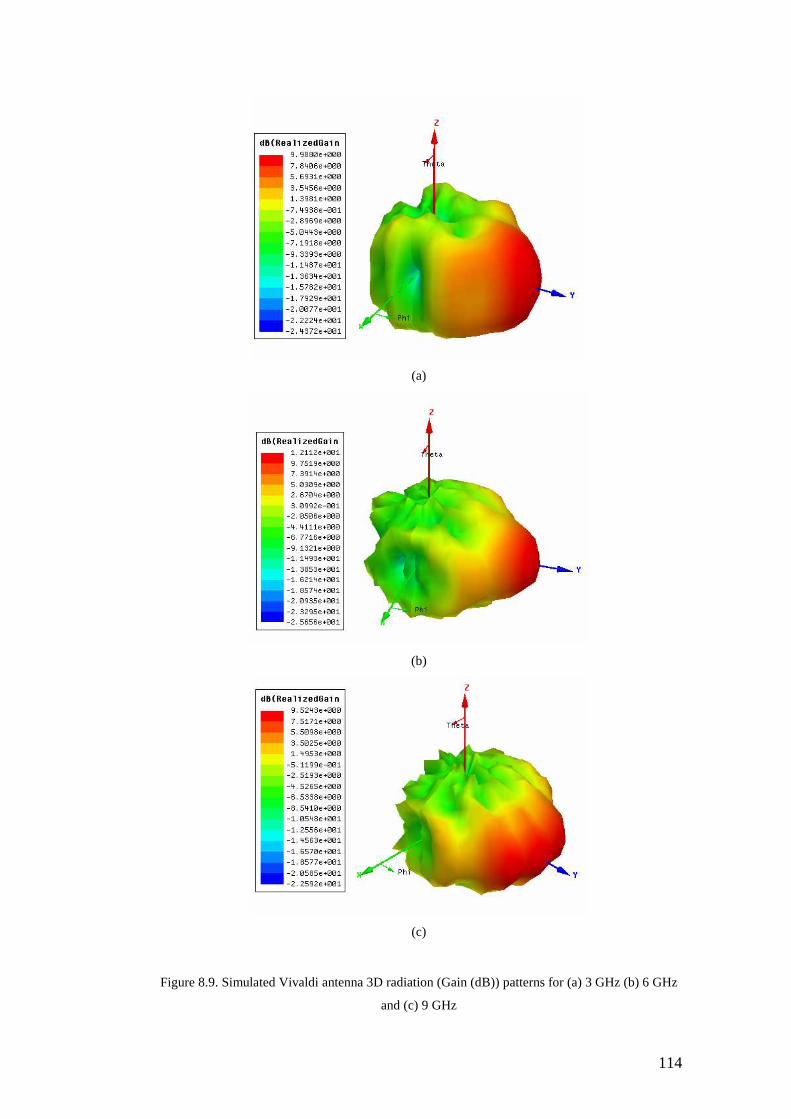
114
(a)
(b)
(c)
Figure 8.9. Simulated Vivaldi antenna 3D radiation (Gain (dB)) patterns for (a) 3 GHz (b) 6 GHz
and (c) 9 GHz

115
The waveform in the previous Figure 8.3 (b) was used as the input to the transmit
antenna and the pulse received is shown in Figure 8.10.
Figure 8.10. Received pulse for Vivaldi antenna.
The overall results obtained for the Vivaldi were considered to be favourable
towards the use of UWB. While it did not have an omni-directional radiation
pattern, nor small size (30cm x 18cm), the results for pulse transmission were
good as it transmitted a pulse with low dispersion. Possible reasons behind the
low pulse dispersion were:
• good group delay
• constant radiation pattern over the operational band in the direction of
transmission i.e. highly directive
• Acceptable impedance bandwidth over operational bandwidth
The Vivaldi meets many of the performance metrics stated in section 8.2 except
compactness and an omni-directional radiation pattern. To compare the Vivaldi
performance another UWB antenna was investigated that was small and omni-
directional. This is discussed in the following section.
8.2.2 The CPW-fed Monopole Antenna
There have been many papers published on the use of planar monopoles for UWB
applications [11]. The CPW-fed wideband monopole antenna presented by
500 ps/division
Vpk-pk≈ 300mV
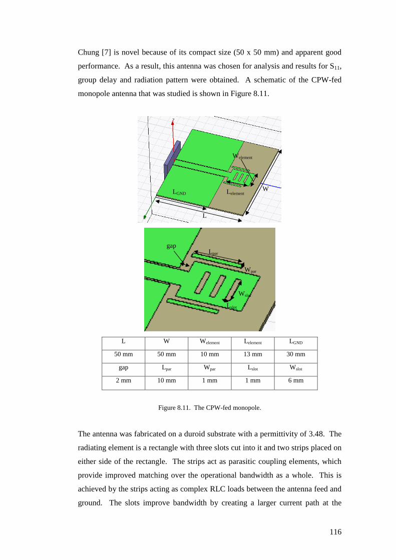
116
Chung [7] is novel because of its compact size (50 x 50 mm) and apparent good
performance. As a result, this antenna was chosen for analysis and results for S11,
group delay and radiation pattern were obtained. A schematic of the CPW-fed
monopole antenna that was studied is shown in Figure 8.11.
L W Welement Lelement LGND
50 mm 50 mm 10 mm 13 mm 30 mm
gap Lpar Wpar Lslot Wslot
2 mm 10 mm 1 mm 1 mm 6 mm
Figure 8.11. The CPW-fed monopole.
The antenna was fabricated on a duroid substrate with a permittivity of 3.48. The
radiating element is a rectangle with three slots cut into it and two strips placed on
either side of the rectangle. The strips act as parasitic coupling elements, which
provide improved matching over the operational bandwidth as a whole. This is
achieved by the strips acting as complex RLC loads between the antenna feed and
ground. The slots improve bandwidth by creating a larger current path at the
L
W LGND
Lpar
Wpar
Welement
Lelement
Wslot
Lslot
gap
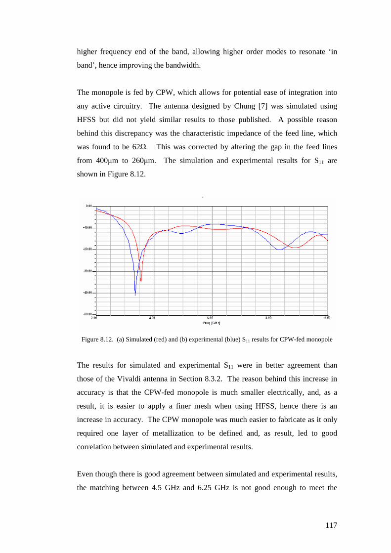
117
higher frequency end of the band, allowing higher order modes to resonate ‘in
band’, hence improving the bandwidth.
The monopole is fed by CPW, which allows for potential ease of integration into
any active circuitry. The antenna designed by Chung [7] was simulated using
HFSS but did not yield similar results to those published. A possible reason
behind this discrepancy was the characteristic impedance of the feed line, which
was found to be 62Ω. This was corrected by altering the gap in the feed lines
from 400µm to 260µm. The simulation and experimental results for S11 are
shown in Figure 8.12.
Figure 8.12. (a) Simulated (red) and (b) experimental (blue) S11 results for CPW-fed monopole
The results for simulated and experimental S11 were in better agreement than
those of the Vivaldi antenna in Section 8.3.2. The reason behind this increase in
accuracy is that the CPW-fed monopole is much smaller electrically, and, as a
result, it is easier to apply a finer mesh when using HFSS, hence there is an
increase in accuracy. The CPW monopole was much easier to fabricate as it only
required one layer of metallization to be defined and, as result, led to good
correlation between simulated and experimental results.
Even though there is good agreement between simulated and experimental results,
the matching between 4.5 GHz and 6.25 GHz is not good enough to meet the
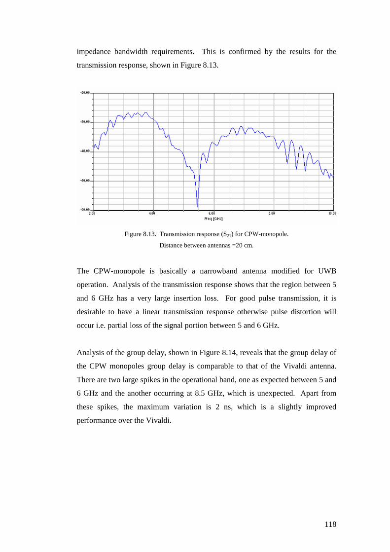
118
impedance bandwidth requirements. This is confirmed by the results for the
transmission response, shown in Figure 8.13.
Figure 8.13. Transmission response (S21) for CPW-monopole.
Distance between antennas =20 cm.
The CPW-monopole is basically a narrowband antenna modified for UWB
operation. Analysis of the transmission response shows that the region between 5
and 6 GHz has a very large insertion loss. For good pulse transmission, it is
desirable to have a linear transmission response otherwise pulse distortion will
occur i.e. partial loss of the signal portion between 5 and 6 GHz.
Analysis of the group delay, shown in Figure 8.14, reveals that the group delay of
the CPW monopoles group delay is comparable to that of the Vivaldi antenna.
There are two large spikes in the operational band, one as expected between 5 and
6 GHz and the another occurring at 8.5 GHz, which is unexpected. Apart from
these spikes, the maximum variation is 2 ns, which is a slightly improved
performance over the Vivaldi.
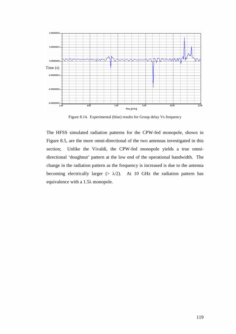
119
Figure 8.14. Experimental (blue) results for Group delay Vs frequency
The HFSS simulated radiation patterns for the CPW-fed monopole, shown in
Figure 8.5, are the more omni-directional of the two antennas investigated in this
section; Unlike the Vivaldi, the CPW-fed monopole yields a true omni-
directional ‘doughnut’ pattern at the low end of the operational bandwidth. The
change in the radiation pattern as the frequency is increased is due to the antenna
becoming electrically larger (> λ/2). At 10 GHz the radiation pattern has
equivalence with a 1.5λ monopole.
Time (s)

120
(a)
(b)
(c)
Figure 8.15. Simulated radiation patterns for (a) 3 GHz (b) 6 GHz and (c) 9 GHz
The CPW-fed monopole had worse performance in terms of pulse distortion.
Inspection of the received pulse, shown in Figure 8.16, shows the effects of
‘ringing’. The reasons behind this are considered to be as follows:
• Large insertion loss in the middle of the band
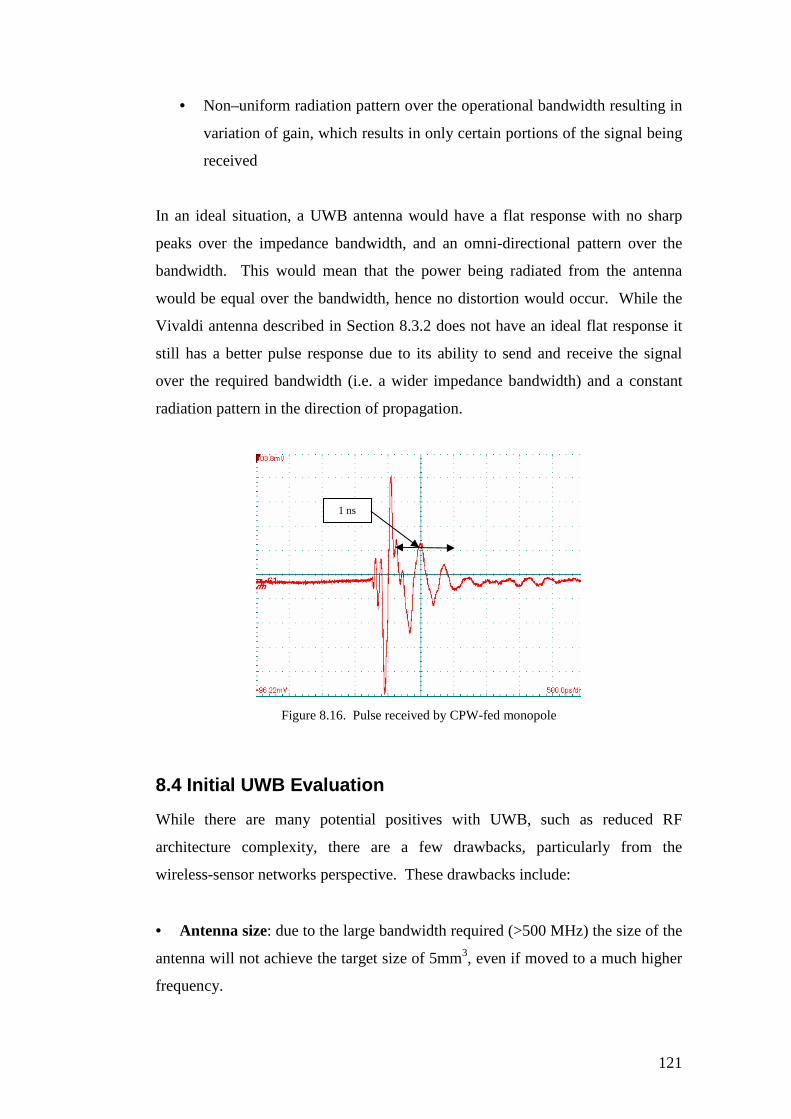
121
• Non–uniform radiation pattern over the operational bandwidth resulting in
variation of gain, which results in only certain portions of the signal being
received
In an ideal situation, a UWB antenna would have a flat response with no sharp
peaks over the impedance bandwidth, and an omni-directional pattern over the
bandwidth. This would mean that the power being radiated from the antenna
would be equal over the bandwidth, hence no distortion would occur. While the
Vivaldi antenna described in Section 8.3.2 does not have an ideal flat response it
still has a better pulse response due to its ability to send and receive the signal
over the required bandwidth (i.e. a wider impedance bandwidth) and a constant
radiation pattern in the direction of propagation.
Figure 8.16. Pulse received by CPW-fed monopole
8.4 Initial UWB Evaluation
While there are many potential positives with UWB, such as reduced RF
architecture complexity, there are a few drawbacks, particularly from the
wireless-sensor networks perspective. These drawbacks include:
• Antenna size: due to the large bandwidth required (>500 MHz) the size of the
antenna will not achieve the target size of 5mm3, even if moved to a much higher
frequency.
1 ns
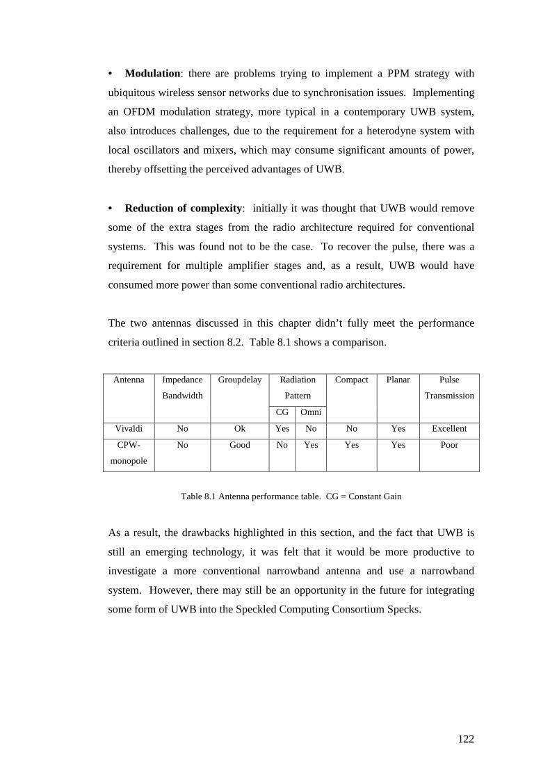
122
• Modulation : there are problems trying to implement a PPM strategy with
ubiquitous wireless sensor networks due to synchronisation issues. Implementing
an OFDM modulation strategy, more typical in a contemporary UWB system,
also introduces challenges, due to the requirement for a heterodyne system with
local oscillators and mixers, which may consume significant amounts of power,
thereby offsetting the perceived advantages of UWB.
• Reduction of complexity: initially it was thought that UWB would remove
some of the extra stages from the radio architecture required for conventional
systems. This was found not to be the case. To recover the pulse, there was a
requirement for multiple amplifier stages and, as a result, UWB would have
consumed more power than some conventional radio architectures.
The two antennas discussed in this chapter didn’t fully meet the performance
criteria outlined in section 8.2. Table 8.1 shows a comparison.
Radiation
Pattern
Antenna Impedance
Bandwidth
Groupdelay
CG Omni
Compact Planar Pulse
Transmission
Vivaldi No Ok Yes No No Yes Excellent
CPW-
monopole
No Good No Yes Yes Yes Poor
Table 8.1 Antenna performance table. CG = Constant Gain
As a result, the drawbacks highlighted in this section, and the fact that UWB is
still an emerging technology, it was felt that it would be more productive to
investigate a more conventional narrowband antenna and use a narrowband
system. However, there may still be an opportunity in the future for integrating
some form of UWB into the Speckled Computing Consortium Specks.
123
9. A UWB channel modelling experiment
An important aspect of the Speckled Computing Consortium research is the
opportunity to undertake interdisciplinary research. One such example was a
UWB channel modelling experiment led by the Strathclyde University signal
processing group. As the expertise of Strathclyde lay with signal processing and
not antenna design, the onus fell on Glasgow to design a suitable antenna. The
design criteria for the antenna was that it operated from 3.16 to 10.6 GHz, be
omni-directional, have relatively standard gain and a good phase response over
the band. As none of the antennas investigated in chapter 8 fully met the criteria,
there was a need for a different type of antenna. The antenna chosen was the
UWB dipole. The test system and design of the antennas will now be considered.
9.1 UWB test system
A channel can be modelled physically by calculating the various processes which
modify the transmitted signal. For example, in wireless communications, the
channel can be modelled by calculating reflection from every object in the
environment. The channel modelling experiment carried out at Strathclyde
University was to determine the impact on sending and receiving a UWB pulse of
the antennas discussed in this chapter.
Figure 9.1 shows the block diagram of the test system, although this will be
covered in greater detail in Section 9.6. For the transmission results discussed in
this chapter, the antennas were placed 20 cm apart from each other, and both
antennas elements were aligned so they were in boresight i.e. the direction of
transmission was perpendicular to the antenna elements. All the antennas are
operating outside the far-field boundary specified by λ/2 2D except the antenna
section 9.2.4 due to a large transmission line feed. Section 9.2.4 compares the
field of a half-wavelength dipole to that of the antenna under investigation. The
field plot is then used to evaluate whether or not the feed should be included in
the maximum linear dimension, D, for the far-field boundary calculation.

124
Figure 9.1 Block diagram for Strathclyde UWB test sytem
Also used in the experiments was an Agilent technologies N5230A 10 MHz – 20
GHz PNA series network analyser. This was used to obtain transmission and
reflection coefficients for the antennas.
9.2 UWB dipole
In 2002, Schanz published a paper on a UWB planar elliptical dipole [1]. Since
then, there have been many published papers on this class of antenna. The main
consideration, apart from the shape, when designing UWB dipoles is the feed
configuration into the antenna element. There are three potential feeding points
for this antenna illustrated in Figure 9.2.
Figure 9.2. Elliptical dipole element with suggested feeding points (a) centre
(b) bottom and (c) edge.
Agilent Infinium D5081204A 12 GHz 40 G Sa/s Comms Analyser
Picosecond Pulse Labs Model 10,060 A Pulse Generator
Pulse shaper (High Pass Filter)
Tx Antenna Rx Antenna
(b)
(c)
(a)
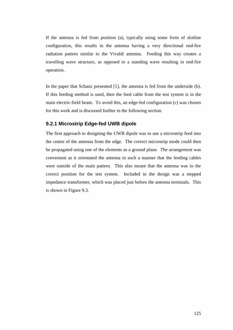
125
If the antenna is fed from position (a), typically using some form of slotline
configuration, this results in the antenna having a very directional end-fire
radiation pattern similar to the Vivaldi antenna. Feeding this way creates a
travelling wave structure, as opposed to a standing wave resulting in end-fire
operation.
In the paper that Schanz presented [1], the antenna is fed from the underside (b).
If this feeding method is used, then the feed cable from the test system is in the
main electric-field beam. To avoid this, an edge-fed configuration (c) was chosen
for this work and is discussed further in the following section.
9.2.1 Microstrip Edge-fed UWB dipole
The first approach to designing the UWB dipole was to use a microstrip feed into
the centre of the antenna from the edge. The correct microstrip mode could then
be propagated using one of the elements as a ground plane. The arrangement was
convenient as it orientated the antenna in such a manner that the feeding cables
were outside of the main pattern. This also meant that the antenna was in the
correct position for the test system. Included in the design was a stepped
impedance transformer, which was placed just before the antenna terminals. This
is shown in Figure 9.3.
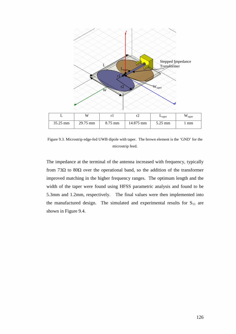
126
L W r1 r2 Ltaper Wtaper
35.25 mm 29.75 mm 8.75 mm 14.875 mm 5.25 mm 1 mm
Figure 9.3. Microstrip edge-fed UWB dipole with taper. The brown element is the ‘GND’ for the
microstrip feed.
The impedance at the terminal of the antenna increased with frequency, typically
from 73Ω to 80Ω over the operational band, so the addition of the transformer
improved matching in the higher frequency ranges. The optimum length and the
width of the taper were found using HFSS parametric analysis and found to be
5.3mm and 1.2mm, respectively. The final values were then implemented into
the manufactured design. The simulated and experimental results for S11 are
shown in Figure 9.4.
Stepped Impedance Transformer L
W r2
r1
Wtaper
Ltaper

127
Figure 9.4. Simulated (blue) and experimental (red) results for S11 Vs. Frequency
The discrepancy in the results was traced to the impact of the cables used to
connect the network analyser to the antenna. Although the cable was positioned
out of the far-field radiation pattern it was almost certainly being excited by the
reactive near-field. This is shown later in section 9.2.2.1. At the position
indicated by Figure 9.1 (c) there was an area of high electric field, particularly at
the lower end of the band. The electric field excites the leakage current along the
length of cable, which means that the feed cable becomes part of the antenna and,
as a result, increases the amount of modes present. The distortion on the plot in
the frequency range from 2 to 6 GHz seen on the experimental S11 results is
evidence of this effect. The effect is also seen in experimental results for phase,
shown in Figure 9.5.
S11Mag(dB)
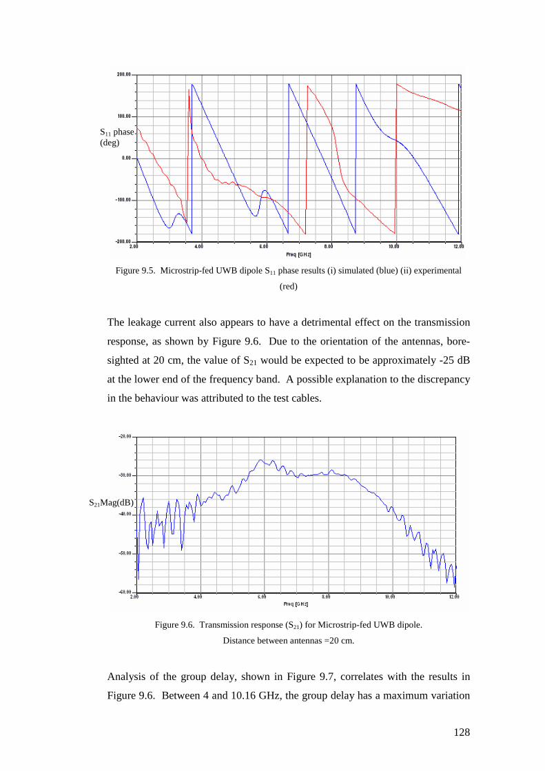
128
Figure 9.5. Microstrip-fed UWB dipole S11 phase results (і) simulated (blue) (іі) experimental
(red)
The leakage current also appears to have a detrimental effect on the transmission
response, as shown by Figure 9.6. Due to the orientation of the antennas, bore-
sighted at 20 cm, the value of S21 would be expected to be approximately -25 dB
at the lower end of the frequency band. A possible explanation to the discrepancy
in the behaviour was attributed to the test cables.
Figure 9.6. Transmission response (S21) for Microstrip-fed UWB dipole.
Distance between antennas =20 cm.
Analysis of the group delay, shown in Figure 9.7, correlates with the results in
Figure 9.6. Between 4 and 10.16 GHz, the group delay has a maximum variation
S11 phase (deg)
S21Mag(dB)
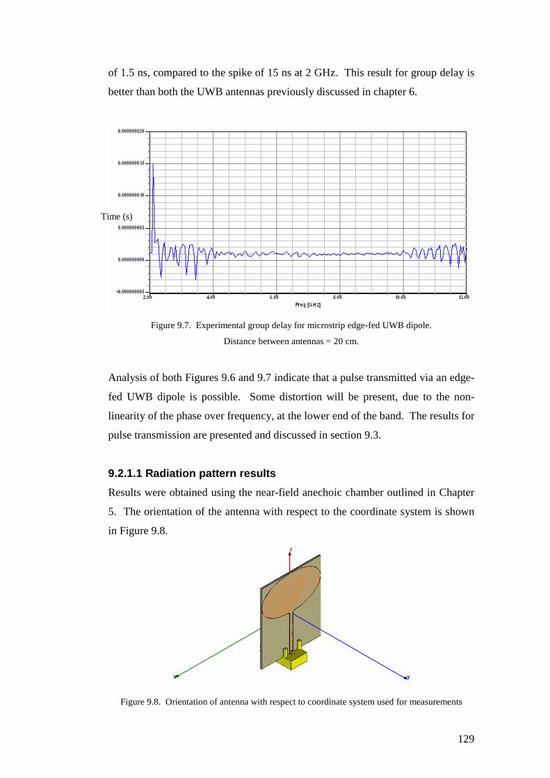
129
of 1.5 ns, compared to the spike of 15 ns at 2 GHz. This result for group delay is
better than both the UWB antennas previously discussed in chapter 6.
Figure 9.7. Experimental group delay for microstrip edge-fed UWB dipole.
Distance between antennas = 20 cm.
Analysis of both Figures 9.6 and 9.7 indicate that a pulse transmitted via an edge-
fed UWB dipole is possible. Some distortion will be present, due to the non-
linearity of the phase over frequency, at the lower end of the band. The results for
pulse transmission are presented and discussed in section 9.3.
9.2.1.1 Radiation pattern results
Results were obtained using the near-field anechoic chamber outlined in Chapter
5. The orientation of the antenna with respect to the coordinate system is shown
in Figure 9.8.
Figure 9.8. Orientation of antenna with respect to coordinate system used for measurements
Time (s)

130
The results for the simulated 3D radiation patterns for electric field in decibels are
shown in Figure 9.9. Analyses of the patterns indicate that the antenna is acting
as a half-wave dipole at 3 GHz through to a 1.5 wavelength dipole at 9 GHz, as
predicted by the theory in Chapter 2, section 2.7.
(a)
(b)

131
(c)
Figure 9.9. Microstrip edge-fed UWB dipole simulated 3D E-field radiation patterns for (a) 3 GHz
(b) 6 GHz and (c) 9 GHz
The radiation plot at 3 GHz, shown in Figure 9.9 (a), highlights the discrepancy in
the transmission results from Figure 9.6, as we would expect a higher gain as
there is maximum gain in z-axis direction.
The simulated and experimental results for the radiation patterns at 3, 6 and 9
GHz are shown in Figure 9.10 in the form of horizontal and vertical cuts.
100 50 0 50 100
30
20
10
0
⟨ ⟩ ⟨ ⟩
200 100 0 100 20040
20
0
⟨ ⟩ ⟨ ⟩
V (dB)
Theta (θ) Phi (φ )
V (dB)
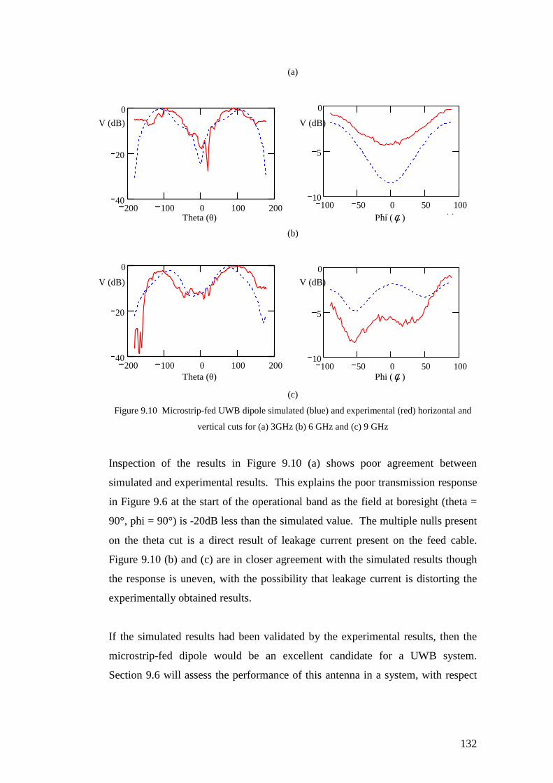
132
(a)
(b)
(c)
Figure 9.10 Microstrip-fed UWB dipole simulated (blue) and experimental (red) horizontal and
vertical cuts for (a) 3GHz (b) 6 GHz and (c) 9 GHz
Inspection of the results in Figure 9.10 (a) shows poor agreement between
simulated and experimental results. This explains the poor transmission response
in Figure 9.6 at the start of the operational band as the field at boresight (theta =
90°, phi = 90°) is -20dB less than the simulated value. The multiple nulls present
on the theta cut is a direct result of leakage current present on the feed cable.
Figure 9.10 (b) and (c) are in closer agreement with the simulated results though
the response is uneven, with the possibility that leakage current is distorting the
experimentally obtained results.
If the simulated results had been validated by the experimental results, then the
microstrip-fed dipole would be an excellent candidate for a UWB system.
Section 9.6 will assess the performance of this antenna in a system, with respect
100 50 0 50 10010
5
0
⟨ ⟩ ⟨ ⟩
200 100 0 100 20040
20
0
100 50 0 50 10010
5
0
⟨ ⟩ ⟨ ⟩
200 100 0 100 20040
20
0
⟨ ⟩ ⟨ ⟩
V (dB)
V (dB)
Phi (φ )
Phi (φ )
V (dB)
V (dB)
Theta (θ)
Theta (θ)
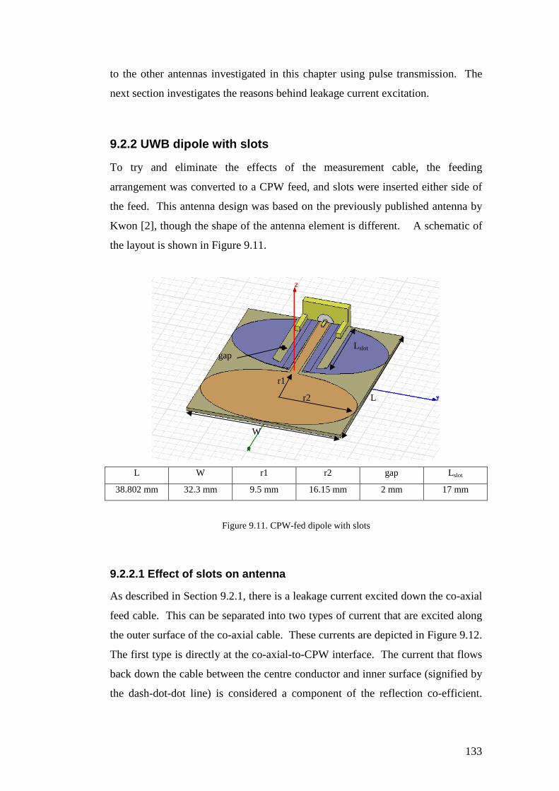
133
to the other antennas investigated in this chapter using pulse transmission. The
next section investigates the reasons behind leakage current excitation.
9.2.2 UWB dipole with slots
To try and eliminate the effects of the measurement cable, the feeding
arrangement was converted to a CPW feed, and slots were inserted either side of
the feed. This antenna design was based on the previously published antenna by
Kwon [2], though the shape of the antenna element is different. A schematic of
the layout is shown in Figure 9.11.
L W r1 r2 gap Lslot
38.802 mm 32.3 mm 9.5 mm 16.15 mm 2 mm 17 mm
Figure 9.11. CPW-fed dipole with slots
9.2.2.1 Effect of slots on antenna
As described in Section 9.2.1, there is a leakage current excited down the co-axial
feed cable. This can be separated into two types of current that are excited along
the outer surface of the co-axial cable. These currents are depicted in Figure 9.12.
The first type is directly at the co-axial-to-CPW interface. The current that flows
back down the cable between the centre conductor and inner surface (signified by
the dash-dot-dot line) is considered a component of the reflection co-efficient.
W
Lslot
L
gap
r1
r2
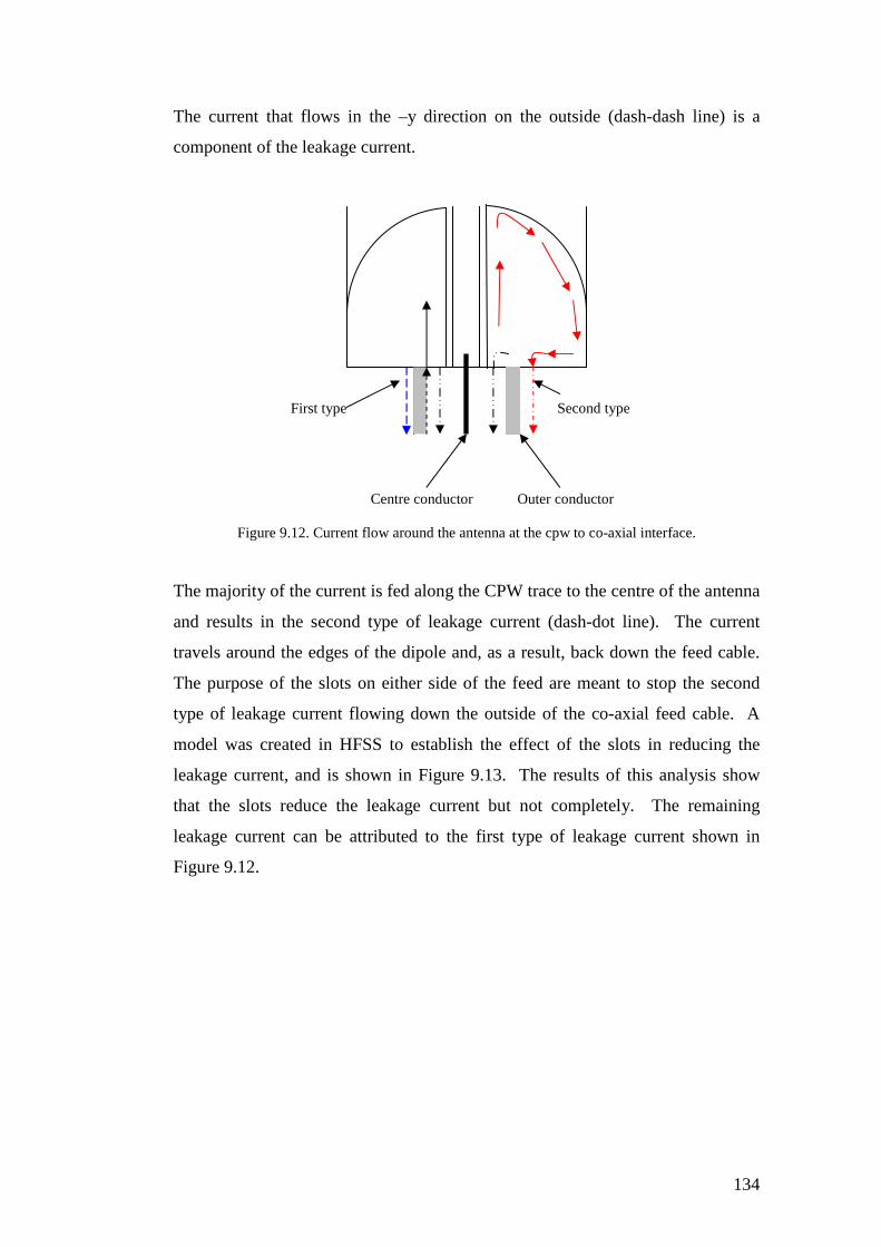
134
The current that flows in the –y direction on the outside (dash-dash line) is a
component of the leakage current.
Figure 9.12. Current flow around the antenna at the cpw to co-axial interface.
The majority of the current is fed along the CPW trace to the centre of the antenna
and results in the second type of leakage current (dash-dot line). The current
travels around the edges of the dipole and, as a result, back down the feed cable.
The purpose of the slots on either side of the feed are meant to stop the second
type of leakage current flowing down the outside of the co-axial feed cable. A
model was created in HFSS to establish the effect of the slots in reducing the
leakage current, and is shown in Figure 9.13. The results of this analysis show
that the slots reduce the leakage current but not completely. The remaining
leakage current can be attributed to the first type of leakage current shown in
Figure 9.12.
First type Second type
Centre conductor Outer conductor
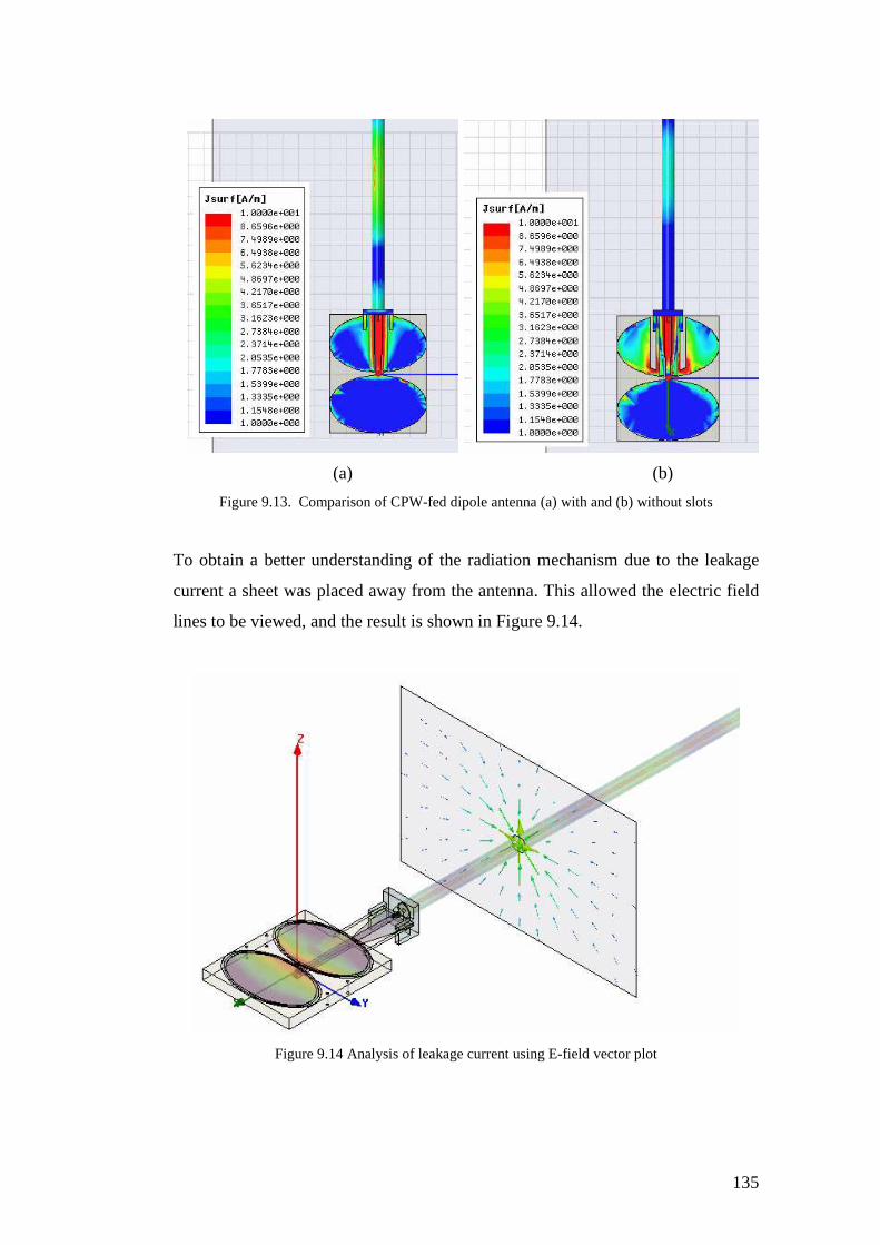
135
(a) (b)
Figure 9.13. Comparison of CPW-fed dipole antenna (a) with and (b) without slots
To obtain a better understanding of the radiation mechanism due to the leakage
current a sheet was placed away from the antenna. This allowed the electric field
lines to be viewed, and the result is shown in Figure 9.14.
Figure 9.14 Analysis of leakage current using E-field vector plot
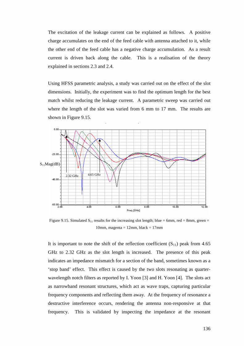
136
The excitation of the leakage current can be explained as follows. A positive
charge accumulates on the end of the feed cable with antenna attached to it, while
the other end of the feed cable has a negative charge accumulation. As a result
current is driven back along the cable. This is a realisation of the theory
explained in sections 2.3 and 2.4.
Using HFSS parametric analysis, a study was carried out on the effect of the slot
dimensions. Initially, the experiment was to find the optimum length for the best
match whilst reducing the leakage current. A parametric sweep was carried out
where the length of the slot was varied from 6 mm to 17 mm. The results are
shown in Figure 9.15.
Figure 9.15. Simulated S11 results for the increasing slot length; blue = 6mm, red = 8mm, green =
10mm, magenta = 12mm, black = 17mm
It is important to note the shift of the reflection coefficient (S11) peak from 4.65
GHz to 2.32 GHz as the slot length is increased. The presence of this peak
indicates an impedance mismatch for a section of the band, sometimes known as a
‘stop band’ effect. This effect is caused by the two slots resonating as quarter-
wavelength notch filters as reported by I. Yoon [3] and H. Yoon [4]. The slots act
as narrowband resonant structures, which act as wave traps, capturing particular
frequency components and reflecting them away. At the frequency of resonance a
destructive interference occurs, rendering the antenna non-responsive at that
frequency. This is validated by inspecting the impedance at the resonant
4.65 GHz 2.32 GHz
S11Mag(dB)
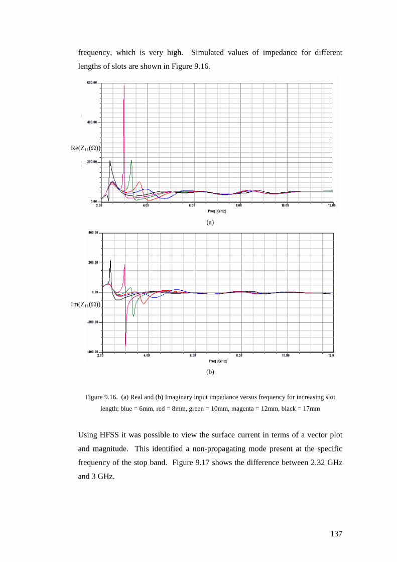
137
frequency, which is very high. Simulated values of impedance for different
lengths of slots are shown in Figure 9.16.
(a)
(b)
Figure 9.16. (a) Real and (b) Imaginary input impedance versus frequency for increasing slot
length; blue = 6mm, red = 8mm, green = 10mm, magenta = 12mm, black = 17mm
Using HFSS it was possible to view the surface current in terms of a vector plot
and magnitude. This identified a non-propagating mode present at the specific
frequency of the stop band. Figure 9.17 shows the difference between 2.32 GHz
and 3 GHz.
Re(Z11(Ω))
Im(Z11(Ω))

138
(a)
(b)
Figure 9.17. (a) Vector surface current plots (a) 2.32 GHz and (b) 3 GHz
The slot = 17 mm for both plots.
Comparing the two plots, the effects of slot at resonance can be clearly seen.
Analysing Figure 9.17 (a), the magnitude of the current is much larger around the
slots and the flow of the current is exactly 180 degrees out of phase along the
length of both sides of the slots. This is the characteristic that causes the antennas
impedance to be much larger than 50Ω. This happens because the net flow of
current across the dipole has been reduced, as shown by Figure 9.16. For the
antenna to radiate in its fundamental mode, the current needs to flow in a uniform
direction across the dipole, as shown by Figure 9.17 (b).
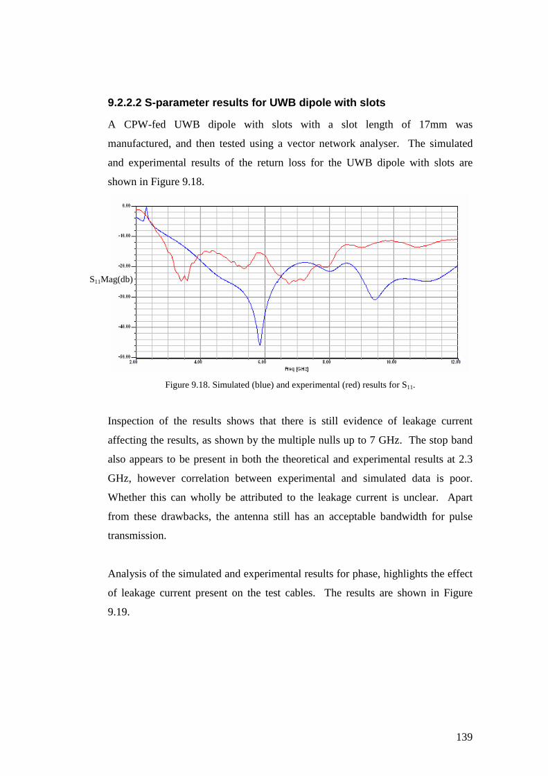
139
9.2.2.2 S-parameter results for UWB dipole with slots
A CPW-fed UWB dipole with slots with a slot length of 17mm was
manufactured, and then tested using a vector network analyser. The simulated
and experimental results of the return loss for the UWB dipole with slots are
shown in Figure 9.18.
Figure 9.18. Simulated (blue) and experimental (red) results for S11.
Inspection of the results shows that there is still evidence of leakage current
affecting the results, as shown by the multiple nulls up to 7 GHz. The stop band
also appears to be present in both the theoretical and experimental results at 2.3
GHz, however correlation between experimental and simulated data is poor.
Whether this can wholly be attributed to the leakage current is unclear. Apart
from these drawbacks, the antenna still has an acceptable bandwidth for pulse
transmission.
Analysis of the simulated and experimental results for phase, highlights the effect
of leakage current present on the test cables. The results are shown in Figure
9.19.
S11Mag(db)
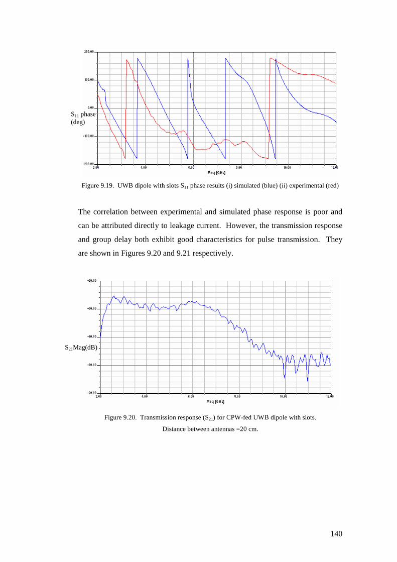
140
Figure 9.19. UWB dipole with slots S11 phase results (і) simulated (blue) (іі) experimental (red)
The correlation between experimental and simulated phase response is poor and
can be attributed directly to leakage current. However, the transmission response
and group delay both exhibit good characteristics for pulse transmission. They
are shown in Figures 9.20 and 9.21 respectively.
Figure 9.20. Transmission response (S21) for CPW-fed UWB dipole with slots.
Distance between antennas =20 cm.
S21Mag(dB)
S11 phase (deg)

141
Figure 9.21. Experimental group delay for UWB dipole with slots.
Distance between antennas = 20 cm.
The UWB dipole with slots exhibits the best transmission response and group
delay results of all the UWB dipoles reviewed in this thesis. The group delay has
a good response since there are no sudden variations in the transmission response
and has a maximum variation of 2ns over the operational bandwidth. Good
transmission response is a result of the radiation patterns of the antenna, which are
discussed in the next section.
9.2.2.3 Radiation pattern results for UWB dipole with slots
Results were obtained using the anechoic chamber outlined in Chapter 5. The
orientation of the antenna with respect to the coordinate system is shown in
Figure 9.22.
Figure 9.22. Orientation of antenna with respect to coordinate system used for measurements
Time(s)

142
The results for the simulated 3D radiation patterns for electric field in decibels are
shown in Figure 9.9. Analyses of the simulated patterns indicate that the antenna
is acting as a half-wave dipole at 3 GHz through to a 1.5 wavelength dipole at 9
GHz, which confirms the theory in chapter 2.
(a)
(b)

143
(c)
Figure 9.23. Simulated 3D E-field radiation patterns for (a) 3 GHz (b) 6 GHz and (c) 9 GHz
The simulated and experimental results for the radiation patterns at 3, 6 and 9
GHz are shown in Figure 9.24 in the form of horizontal and vertical cuts.
(a)
100 50 0 50 1008
6
4
2
200 100 0 100 20060
40
20
0
100 50 0 50 10010
5
0
⟨ ⟩ ⟨ ⟩
200 100 0 100 20040
20
0
⟨ ⟩ ⟨ ⟩
V (dB)
Theta (θ) Phi (φ )
V (dB)
V (dB)
V (dB)
Theta (θ) Phi (φ )
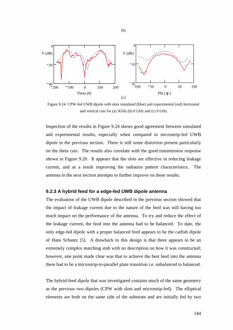
144
(b)
(c)
Figure 9.24 CPW-fed UWB dipole with slots simulated (blue) and experimental (red) horizontal
and vertical cuts for (a) 3GHz (b) 6 GHz and (c) 9 GHz
Inspection of the results in Figure 9.24 shows good agreement between simulated
and experimental results, especially when compared to microstrip-fed UWB
dipole in the previous section. There is still some distortion present particularly
on the theta cuts. The results also correlate with the good transmission response
shown in Figure 9.20. It appears that the slots are effective in reducing leakage
current, and as a result improving the radiation pattern characteristics. The
antenna in the next section attempts to further improve on these results.
9.2.3 A hybrid feed for a edge-fed UWB dipole antenna
The evaluation of the UWB dipole described in the previous section showed that
the impact of leakage current due to the nature of the feed was still having too
much impact on the performance of the antenna. To try and reduce the effect of
the leakage current, the feed into the antenna had to be balanced. To date, the
only edge-fed dipole with a proper balanced feed appears to be the catfish dipole
of Hans Schantz [5]. A drawback to this design is that there appears to be an
extremely complex matching stub with no description on how it was constructed;
however, one point made clear was that to achieve the best feed into the antenna
there had to be a microstrip-to-parallel plate transition i.e. unbalanced to balanced.
The hybrid-feed dipole that was investigated contains much of the same geometry
as the previous two dipoles (CPW with slots and microstrip-fed). The elliptical
elements are both on the same side of the substrate and are initially fed by two
100 50 0 50 10020
10
0
200 100 0 100 20040
20
0
V (dB) V (dB)
Theta (θ) Phi (φ )
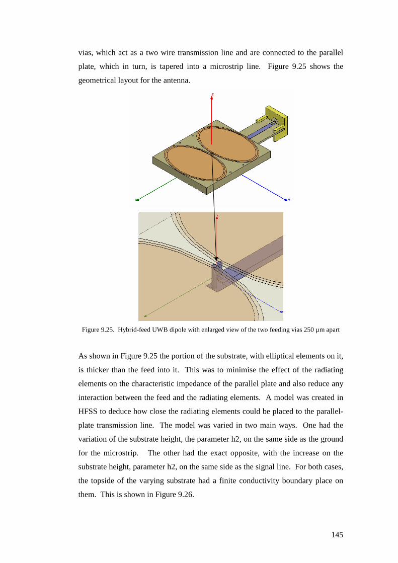
145
vias, which act as a two wire transmission line and are connected to the parallel
plate, which in turn, is tapered into a microstrip line. Figure 9.25 shows the
geometrical layout for the antenna.
Figure 9.25. Hybrid-feed UWB dipole with enlarged view of the two feeding vias 250 µm apart
As shown in Figure 9.25 the portion of the substrate, with elliptical elements on it,
is thicker than the feed into it. This was to minimise the effect of the radiating
elements on the characteristic impedance of the parallel plate and also reduce any
interaction between the feed and the radiating elements. A model was created in
HFSS to deduce how close the radiating elements could be placed to the parallel-
plate transmission line. The model was varied in two main ways. One had the
variation of the substrate height, the parameter h2, on the same side as the ground
for the microstrip. The other had the exact opposite, with the increase on the
substrate height, parameter h2, on the same side as the signal line. For both cases,
the topside of the varying substrate had a finite conductivity boundary place on
them. This is shown in Figure 9.26.

146
(a)
(b)
L W h1 h2 LGND
32.025 mm 9.5 mm 0.762 mm 2.286 mm 7.9375 mm
Figure 9.26. HFSS model for parallel plate interaction with metal (a) GND clear (b) signal clear
Both models were parametrically analysed with the substrate height increased in
increments of 0.762mm, which was the standard substrate height for the Rogers
4350 board. If there was a separation of one board, then there was substantial
coupling into the metal creating a stripline mode. Through parametric analysis, it
was found for both models that an acceptable amount of coupling was achieved
by using a three substrate thickness of h2 = 2.286 mm. Results for return and
insertion loss for both models are shown in Figure 9.27 and 9.28 respectively.
h1
h1 + h2
W
L
L
h1 + h2
h1
W
LGND
Finite conductivity boundary placed on top of substrate with height h2

147
(a)
Figure 9.27. S11 and S22 for sub thickness = 2.286 mm; Blue (S11) and Red (S22) belong to signal
clear (Figure 9.26 (b)); Green (S11) and Magenta (S22) belong to GND clear (Figure 9.26 (a)).
Figure 9.28 Insertion Loss for sub thickness = 2.286 mm – GND clear (blue), Signal clear (red).
Throughout the analysis of the two models, it was apparent that having the
microstrip ground on the side that was opposite to side of the antenna elements
would give a significantly better performance. A possible explanation to this
behaviour was that as the ground was clear, it gave a better balance in terms of
field manipulation to the signal, and less dispersion occurred when it entered into
the thicker substrate.
With the substrate height and feeding arrangement optimised, the full model was
created. The most critical part of the design was the gap between the two
S11Mag(db)
S21Mag(db)

148
radiating elements, which determined the input impedance for the antenna. This
gap was optimised by placing a lumped port between the two wire transmission
lines. This determined the optimum gap between the two elements and indicated
what the impedance of the parallel plate feeding into the two wire feed should be.
After this was determined, the full model was analysed with feed coming from the
SMA connector. The antenna was optimised further by running parametric
analysis on the tapering between the microstrip and the parallel plate. Figure 9.29
shows different views of the antenna with the various optimum dimensions
outlined.
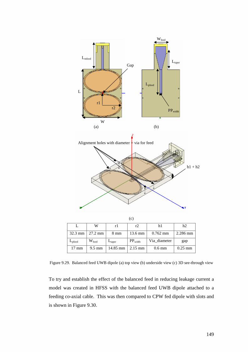
149
(a) (b)
(c)
L W r1 r2 h1 h2
32.3 mm 27.2 mm 8 mm 13.6 mm 0.762 mm 2.286 mm
Lpfeed Wfeed Ltaper PPwidth Via_diameter gap
17 mm 9.5 mm 14.85 mm 2.15 mm 0.6 mm 0.25 mm
Figure 9.29. Balanced feed UWB dipole (a) top view (b) underside view (c) 3D see-through view
To try and establish the effect of the balanced feed in reducing leakage current a
model was created in HFSS with the balanced feed UWB dipole attached to a
feeding co-axial cable. This was then compared to CPW fed dipole with slots and
is shown in Figure 9.30.
L
W
Lmfeed
Alignment holes with diameter = via for feed
Gap
r1 r2
Lpfeed
Ltaper
PPwidth
Wfeed
h1 + h2
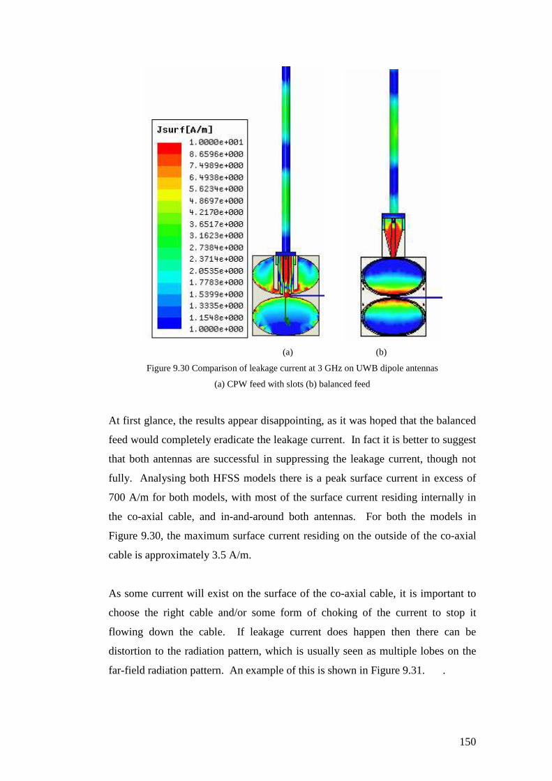
150
(a) (b)
Figure 9.30 Comparison of leakage current at 3 GHz on UWB dipole antennas
(a) CPW feed with slots (b) balanced feed
At first glance, the results appear disappointing, as it was hoped that the balanced
feed would completely eradicate the leakage current. In fact it is better to suggest
that both antennas are successful in suppressing the leakage current, though not
fully. Analysing both HFSS models there is a peak surface current in excess of
700 A/m for both models, with most of the surface current residing internally in
the co-axial cable, and in-and-around both antennas. For both the models in
Figure 9.30, the maximum surface current residing on the outside of the co-axial
cable is approximately 3.5 A/m.
As some current will exist on the surface of the co-axial cable, it is important to
choose the right cable and/or some form of choking of the current to stop it
flowing down the cable. If leakage current does happen then there can be
distortion to the radiation pattern, which is usually seen as multiple lobes on the
far-field radiation pattern. An example of this is shown in Figure 9.31. .
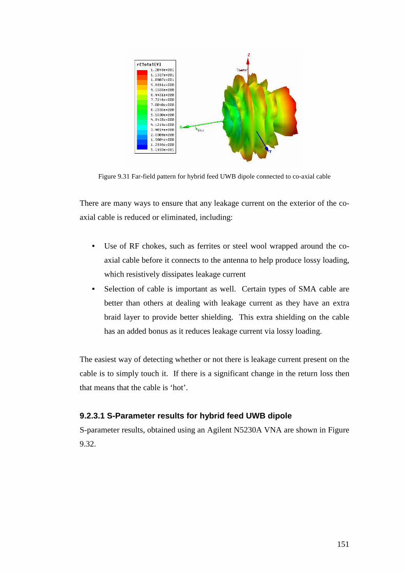
151
Figure 9.31 Far-field pattern for hybrid feed UWB dipole connected to co-axial cable
There are many ways to ensure that any leakage current on the exterior of the co-
axial cable is reduced or eliminated, including:
• Use of RF chokes, such as ferrites or steel wool wrapped around the co-
axial cable before it connects to the antenna to help produce lossy loading,
which resistively dissipates leakage current
• Selection of cable is important as well. Certain types of SMA cable are
better than others at dealing with leakage current as they have an extra
braid layer to provide better shielding. This extra shielding on the cable
has an added bonus as it reduces leakage current via lossy loading.
The easiest way of detecting whether or not there is leakage current present on the
cable is to simply touch it. If there is a significant change in the return loss then
that means that the cable is ‘hot’.
9.2.3.1 S-Parameter results for hybrid feed UWB dipole
S-parameter results, obtained using an Agilent N5230A VNA are shown in Figure
9.32.

152
Figure 9.32. S11 for simulated (blue) and practical (red)
At first inspection, the correlation between simulated and practical results is good,
considering that the analysis is over a large frequency range. The nulls match at
various frequencies, which give confidence that the HFSS model gives an
accurate description of the antenna. The discrepancies that do exist can be
attributed to manufacturing errors since the antenna was engineered by hand. The
vias were particularly hard to drill, and there was no guarantee that the boards
were perfectly aligned.
Figure 9.33 Simulated (blue) and experimental (red) results for phase
S11 phase (deg)
S21Mag(dB)
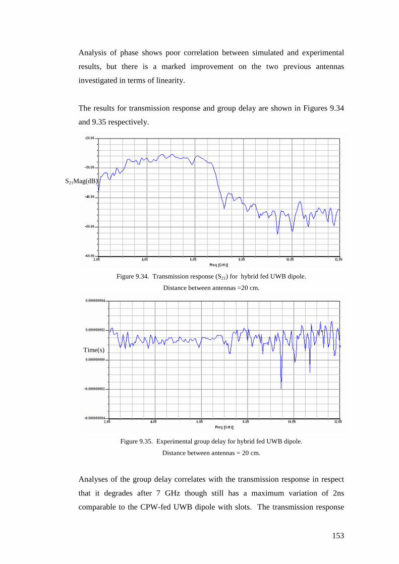
153
Analysis of phase shows poor correlation between simulated and experimental
results, but there is a marked improvement on the two previous antennas
investigated in terms of linearity.
The results for transmission response and group delay are shown in Figures 9.34
and 9.35 respectively.
Figure 9.34. Transmission response (S21) for hybrid fed UWB dipole.
Distance between antennas =20 cm.
Figure 9.35. Experimental group delay for hybrid fed UWB dipole.
Distance between antennas = 20 cm.
Analyses of the group delay correlates with the transmission response in respect
that it degrades after 7 GHz though still has a maximum variation of 2ns
comparable to the CPW-fed UWB dipole with slots. The transmission response
S21Mag(dB)
Time(s)
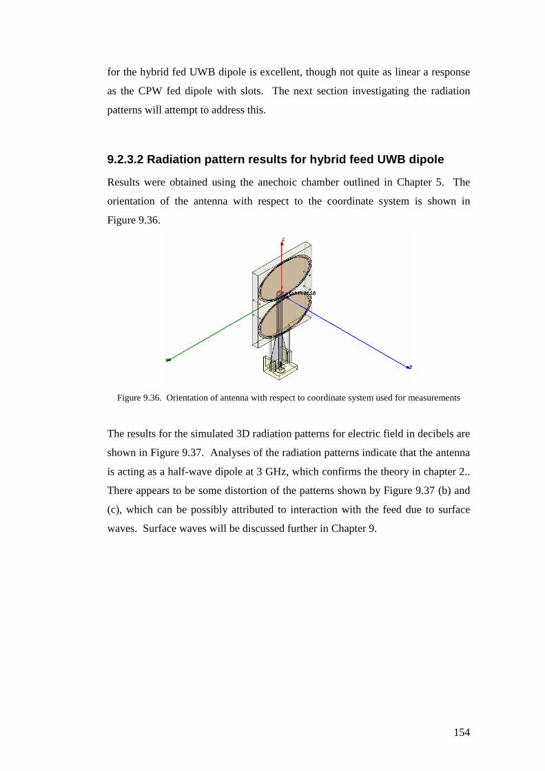
154
for the hybrid fed UWB dipole is excellent, though not quite as linear a response
as the CPW fed dipole with slots. The next section investigating the radiation
patterns will attempt to address this.
9.2.3.2 Radiation pattern results for hybrid feed UWB dipole
Results were obtained using the anechoic chamber outlined in Chapter 5. The
orientation of the antenna with respect to the coordinate system is shown in
Figure 9.36.
Figure 9.36. Orientation of antenna with respect to coordinate system used for measurements
The results for the simulated 3D radiation patterns for electric field in decibels are
shown in Figure 9.37. Analyses of the radiation patterns indicate that the antenna
is acting as a half-wave dipole at 3 GHz, which confirms the theory in chapter 2..
There appears to be some distortion of the patterns shown by Figure 9.37 (b) and
(c), which can be possibly attributed to interaction with the feed due to surface
waves. Surface waves will be discussed further in Chapter 9.
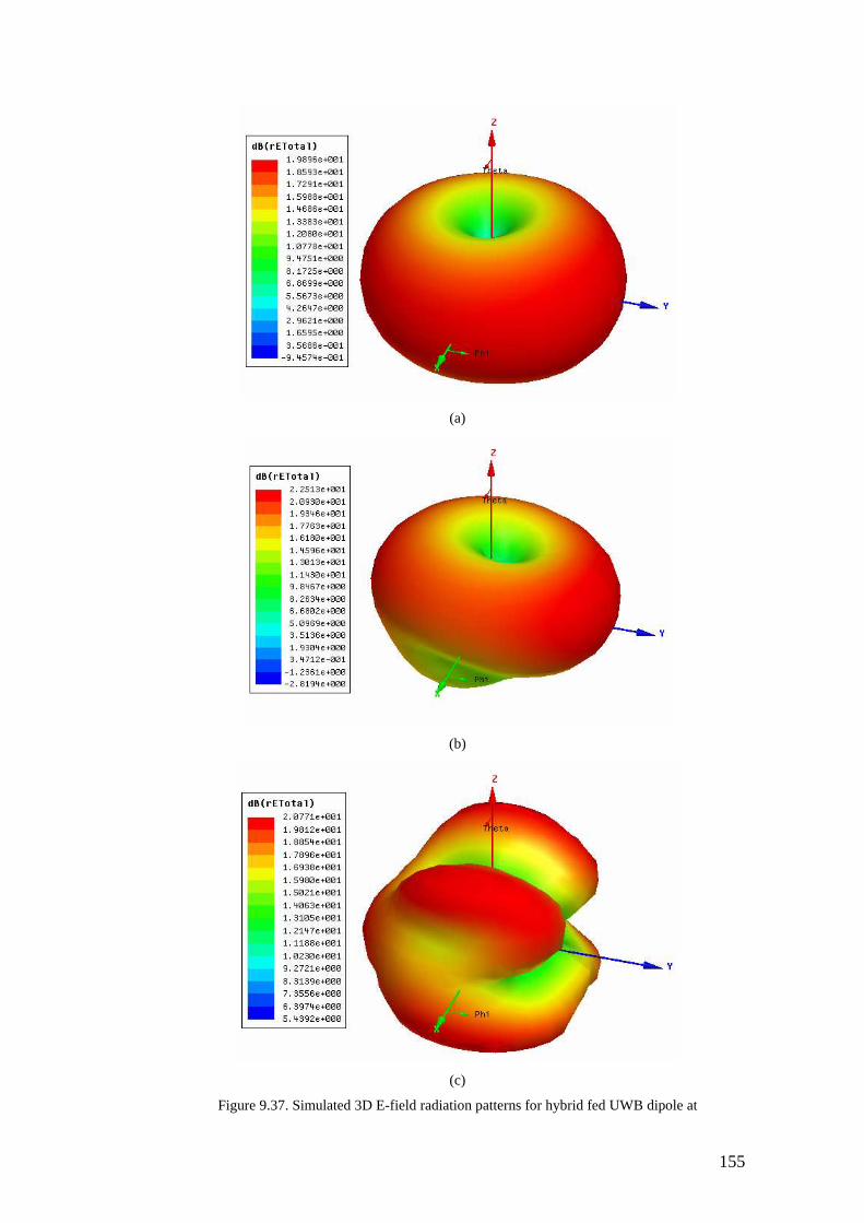
155
(a)
(b)
(c)
Figure 9.37. Simulated 3D E-field radiation patterns for hybrid fed UWB dipole at
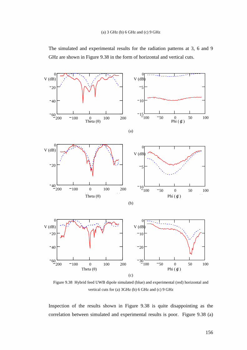
156
(a) 3 GHz (b) 6 GHz and (c) 9 GHz
The simulated and experimental results for the radiation patterns at 3, 6 and 9
GHz are shown in Figure 9.38 in the form of horizontal and vertical cuts.
(a)
(b)
(c)
Figure 9.38 Hybrid feed UWB dipole simulated (blue) and experimental (red) horizontal and
vertical cuts for (a) 3GHz (b) 6 GHz and (c) 9 GHz
Inspection of the results shown in Figure 9.38 is quite disappointing as the
correlation between simulated and experimental results is poor. Figure 9.38 (a)
100 50 0 50 10015
10
5
0
200 100 0 100 20060
40
20
0
100 50 0 50 10010
5
0
⟨ ⟩ ⟨ ⟩
200 100 0 100 20040
20
0
⟨ ⟩ ⟨ ⟩
200 100 0 100 20060
40
20
0
100 50 0 50 10030
20
10
0
⟨ ⟩ ⟨ ⟩
V (dB)
V (dB)
V (dB)
V (dB)
Phi (φ )
Phi (φ )
Theta (θ)
Theta (θ)
Theta (θ)
V (dB) V (dB)
Phi (φ )

157
appears to show evidence of leakage current as there are multiple nulls present
and the signal level at boresight is 10dB less than the simulated value. This poor
result is reciprocated by the value transmission response, shown in Figure 9.34, at
3 GHz. The phi cut for Figure 9.38 (c) possibly explains the sudden drop in the
transmission response at around 7GHz with a large null very close to boresight.
The final antenna analysed in this chapter attempts to completely eradicate the
leakage current present on the cable and is discussed in the next section
9.2.4 A tapered feed UWB dipole
As a result of both the CPW-fed UWB dipole with slots and the hybrid-fed UWB
dipole producing leakage current, it was imperative that an antenna should be
designed that did not allow leakage current. To achieve this goal, a transition was
designed that was based on the microstrip-to-parallel-plate tapered line balun
transformer first introduced by Duncan and Minerva [6]. This balun offers good
broadband performance over an octave of bandwidth. Figure 9.39 shows the
geometrical layout of the balun.
L W Lmicrostrip Wmicrostrip Ltaper LPP WPP
71.6 mm 9.52 mm 6.4 mm 1.7 mm 58.8 mm 6.4 mm 2.25 mm
Figure 9.39. Layout of microstrip to parallel-plate tapered line balun. Overall dimensions - length
= 71.6mm, width = 9.52mm.
The balun in figure 9.39 operates as follows. The signal is inputted into the balun
from a unbalanced source such as a co-axial cable. Co-axial is unbalanced as it
has a current, at any given instant, at any location along the line, which flows on
the centre conductor, and return currents flow on the inside of the surface of the
ground sheath. This configuration is known as an “unbalanced line”. The same
principle applies for microstrip line, which is unbalanced. The balun transforms
L
W
Ltaper Lmicrostrip LPP
WPP Wmicrostrip

158
the signal to the parallel plate waveguide, which consists of a pair of symmetrical
conductors. At any given instant, at any location along the parallel plate
waveguide transmission line, equal and opposite currents flow. This
configuration is known as “balanced”.
The balun was simulated and designed using Rogers 4350 board (permittivity =
3.48). Using HFSS it was possible to manipulate the tapering using three point
arcs on both the top and bottom sections. This allowed for the optimum transition
between the microstrip and the parallel-plate waveguide. The length of the taper
should be approximately at least half a wavelength at the low end of the
operational band. This allows for proper manipulation of the fields from a
microstrip mode (unbalanced) to parallel-plate (balanced) mode. To verify this,
Figure 9.39 shows the surface current plot on both the top and bottom sections.
Figure 9.40. Surface current plot for balun at 3 GHz
A quick inspection of Figure 9.40 verifies that length of the transition is greater
than a half wavelength at lower end of the operational band (3 GHz). Simulated
results for S-parameters after optimisation are shown in Figure 9.40.

159
(a)
(b)
Figure 9.41 Simulated S-parameter results for balun. (a) S21 = Green; S11 = Blue; S22 = Red
(b) S21 phase
As shown by the results in Figure 9.41 the balun offers an excellent transition
over the frequency band of interest. The insertion loss at 10 GHz is just 0.55 dB.
The next stage was to integrate the balun with the elliptical antenna elements.
Due to the nature of the transition, the only way to integrate this was from the
underside, into the centre of the antenna. This is shown in Figure 9.42.
1.00 2.00 3.00 4.00 5.00 6.00 7.00 8.00 9.00 10.00Freq [GHz]
-200.00
-150.00
-100.00
-50.00
0.00
50.00
100.00
150.00
200.00
XY Plot 2
Mag(dB)
Phase (deg)
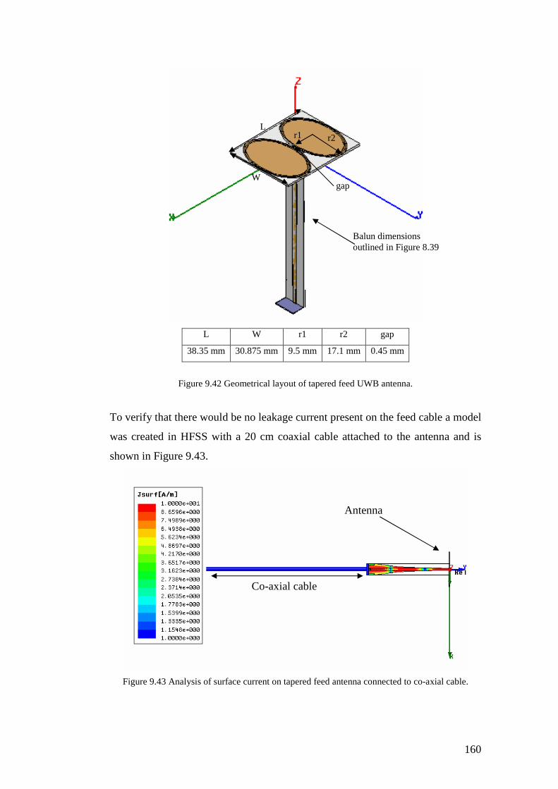
160
L W r1 r2 gap
38.35 mm 30.875 mm 9.5 mm 17.1 mm 0.45 mm
Figure 9.42 Geometrical layout of tapered feed UWB antenna.
To verify that there would be no leakage current present on the feed cable a model
was created in HFSS with a 20 cm coaxial cable attached to the antenna and is
shown in Figure 9.43.
Figure 9.43 Analysis of surface current on tapered feed antenna connected to co-axial cable.
L
W
Antenna
Co-axial cable
Balun dimensions outlined in Figure 8.39
gap
r2 r1
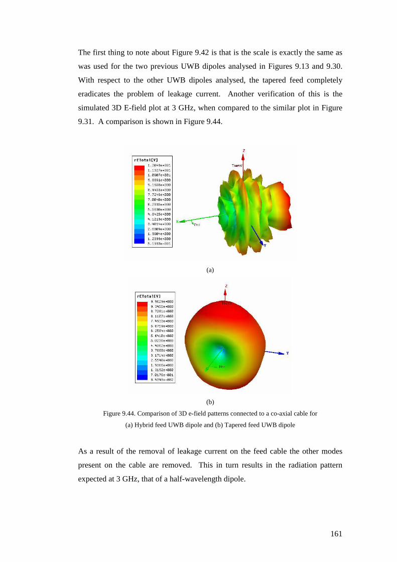
161
The first thing to note about Figure 9.42 is that is the scale is exactly the same as
was used for the two previous UWB dipoles analysed in Figures 9.13 and 9.30.
With respect to the other UWB dipoles analysed, the tapered feed completely
eradicates the problem of leakage current. Another verification of this is the
simulated 3D E-field plot at 3 GHz, when compared to the similar plot in Figure
9.31. A comparison is shown in Figure 9.44.
(a)
(b)
Figure 9.44. Comparison of 3D e-field patterns connected to a co-axial cable for
(a) Hybrid feed UWB dipole and (b) Tapered feed UWB dipole
As a result of the removal of leakage current on the feed cable the other modes
present on the cable are removed. This in turn results in the radiation pattern
expected at 3 GHz, that of a half-wavelength dipole.
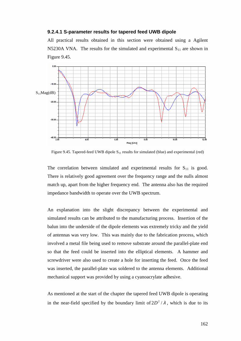
162
9.2.4.1 S-parameter results for tapered feed UWB dipole
All practical results obtained in this section were obtained using a Agilent
N5230A VNA. The results for the simulated and experimental S11 are shown in
Figure 9.45.
Figure 9.45. Tapered-feed UWB dipole S11 results for simulated (blue) and experimental (red)
The correlation between simulated and experimental results for S11 is good.
There is relatively good agreement over the frequency range and the nulls almost
match up, apart from the higher frequency end. The antenna also has the required
impedance bandwidth to operate over the UWB spectrum.
An explanation into the slight discrepancy between the experimental and
simulated results can be attributed to the manufacturing process. Insertion of the
balun into the underside of the dipole elements was extremely tricky and the yield
of antennas was very low. This was mainly due to the fabrication process, which
involved a metal file being used to remove substrate around the parallel-plate end
so that the feed could be inserted into the elliptical elements. A hammer and
screwdriver were also used to create a hole for inserting the feed. Once the feed
was inserted, the parallel-plate was soldered to the antenna elements. Additional
mechanical support was provided by using a cyanoacrylate adhesive.
As mentioned at the start of the chapter the tapered feed UWB dipole is operating
in the near-field specified by the boundary limit of λ/2 2D , which is due to its
S11Mag(dB)
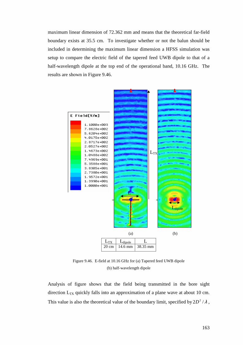
163
maximum linear dimension of 72.362 mm and means that the theoretical far-field
boundary exists at 35.5 cm. To investigate whether or not the balun should be
included in determining the maximum linear dimension a HFSS simulation was
setup to compare the electric field of the tapered feed UWB dipole to that of a
half-wavelength dipole at the top end of the operational band, 10.16 GHz. The
results are shown in Figure 9.46.
(a) (b)
LTX Ldipole L 20 cm 14.6 mm 38.35 mm
Figure 9.46. E-field at 10.16 GHz for (a) Tapered feed UWB dipole
(b) half-wavelength dipole
Analysis of figure shows that the field being transmitted in the bore sight
direction LTX quickly falls into an approximation of a plane wave at about 10 cm.
This value is also the theoretical value of the boundary limit, specified by λ/2 2D ,
Ldipole
LTX
L

164
for a maximum linear dimension of 38.35mm, which equals L for the tapered feed
UWB dipole.
Figure 9.47. Simulated (blue) and experimental (red) results for phase
Analysis of the phase in Figure 9.46 shows good correlation between
experimental and simulated results, especially when compared to the results
obtained from the previous three antennas analysed in this section. At the lower
end of the operational band, the experimental results were out of phase when
compared to the simulated result. However the experimental phase has greater
linearity over the entire band when compared to the simulated results. The
reasons for this are as yet unclear.
Analysis of the transmission response, shown in Figure 9.47, shows excellent
performance up to 9 GHz, where the response drops away quite suddenly to a
very low level. If transmission response did not drop to -60 dB between 9 and 10
GHz then the tapered feed UWB dipole would be outperforming all the antennas
previously discussed in this section.
Phase S11 (deg)

165
Figure 9.48. Transmission response (S21) for tapered feed UWB dipole.
Distance between antennas =20 cm.
Analysis of the group delay, shown in Figure 9.48, reveals a large spike located
between 9 and 10 GHz. At this late stage in the project it is hard to ascertain what
is causing this large degradation in performance for both the transmission and
group delay responses. However, apart from the spike, the tapered feed UWB
dipole has good performance with a maximum variation of 10 ns.
Figure 9.49. Experimental group delay for tapered feed UWB dipole.
Distance between antennas = 20 cm.
S21Mag(dB)

166
9.2.4.2 Radiation pattern results for tapered feed UWB dipole
Results were obtained using the anechoic chamber outlined in Chapter 5. The
orientation of the antenna with respect to the coordinate system is shown in
Figure 9.49.
Figure 9.50. Orientation of antenna with respect to coordinate system used for measurements
The results for the simulated 3D radiation patterns for electric field in decibels are
shown in Figure 9.50. Analyses of the simulated patterns indicate that the
antenna is acting above a half-wave dipole at 3 GHz, hence the slightly misshapen
pattern. This is due to the fundamental frequency being slightly lower, around 2
GHz. The other radiation patterns at 6 and 9 GHz conform to the expected shape,
which confirms the theory in chapter 2.
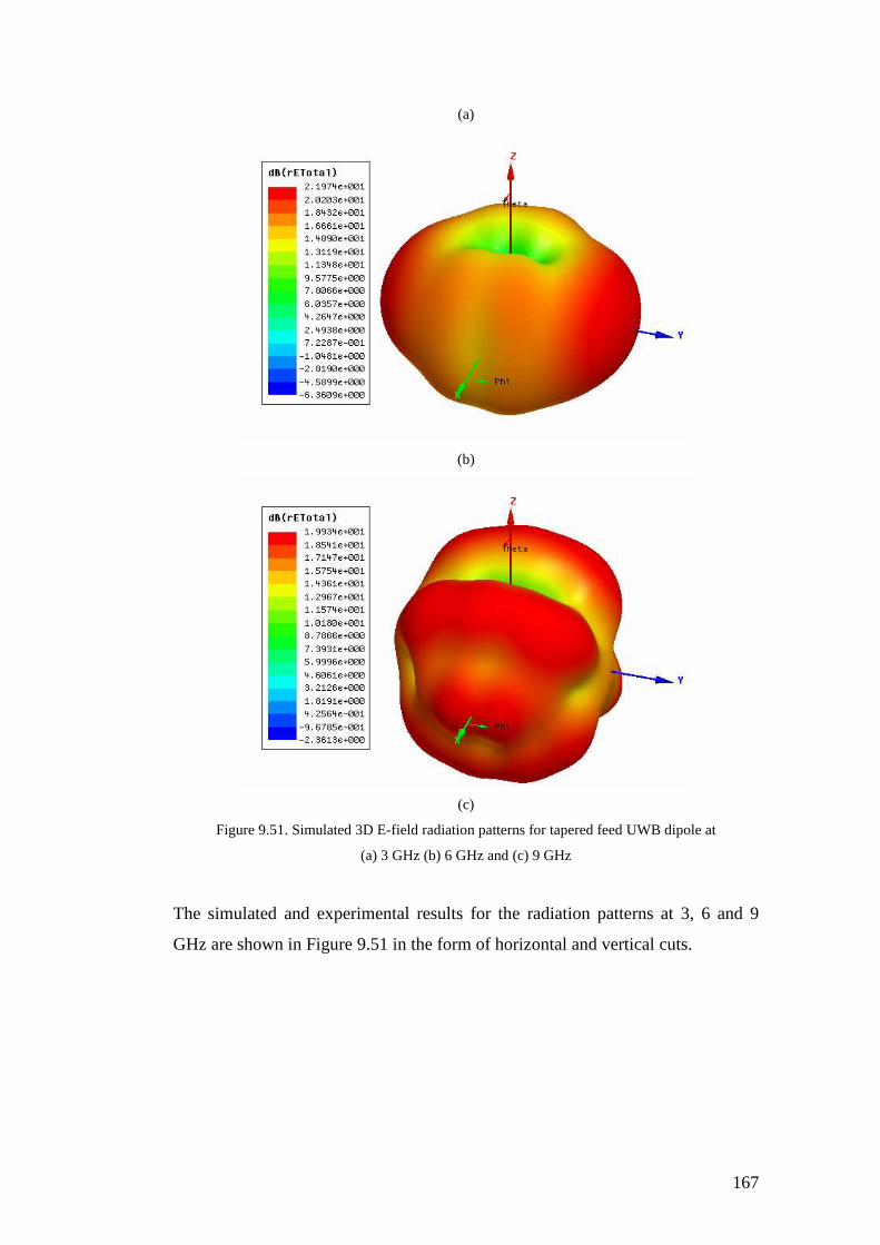
167
(a)
(b)
(c)
Figure 9.51. Simulated 3D E-field radiation patterns for tapered feed UWB dipole at
(a) 3 GHz (b) 6 GHz and (c) 9 GHz
The simulated and experimental results for the radiation patterns at 3, 6 and 9
GHz are shown in Figure 9.51 in the form of horizontal and vertical cuts.

168
(a)
(b)
(c)
Figure 9.52 Tapered feed UWB dipole simulated (blue) and experimental (red) horizontal and
vertical cuts for (a) 3GHz (b) 6 GHz and (c) 9 GHz
Inspection of the results shown in Figure 9.51 show relatively good agreement
between simulated and experimental for the theta cuts. The results for Figure
9.51 (b) and (c) are quite surprising as they are not indicative of leakage current as
the main beam is normal to the feed cable, and as result is normally observed via
the horizontal cut. A possible explanation is that due to the fabrication of the
antenna there is an excitation of another mode due to mismatch at the higher
frequency end of the operational band. Inspection of the S11 response in Figure
9.45 shows three sharp resonances that are not visible on the simulated response.
200 100 0 100 20040
20
0
⟨ ⟩ ⟨ ⟩
100 50 0 50 10010
5
0
21
⟨ ⟩ ⟨ ⟩
100 50 0 50 10015
10
5
0
⟨ ⟩ ⟨ ⟩
200 100 0 100 20040
20
0
⟨ ⟩ ⟨ ⟩
100 50 0 50 10015
10
5
0
⟨ ⟩ ⟨ ⟩
200 100 0 100 20060
40
20
0
⟨ ⟩ ⟨ ⟩
Theta (θ)
V (dB)
Phi (φ )
V (dB)
Theta (θ)
V (dB)
Phi (φ )
V (dB)
V (dB)
Theta (θ)
V (dB)
Phi (φ )

169
This unexpected radiation pattern response may also explain the dip in
transmission response, shown in Figure 9.47, which occurs after 7 GHz. The next
section evaluates the UWB pulse transmission performance of the various
antennas described in this chapter.
9.3 Comparison of UWB dipoles for pulse transmissio n
Once the characterisation of the UWB dipoles was completed the next step was to
evaluate their performance within a UWB test system. The test system used was
the previously shown Figure 9.1.
In UWB engineering the Gaussian family of time domain signals are commonly
used. A Gaussian signal has the mathematical form:
( )2
2
2)( τBt
Aetv−
−= (9.1)
Where,
A = amplitude of signal
B = centre position of peak
τ = half-width of pulse
Using Mathcad [7] an example of a zero order Gaussian pulse is shown in Figure
9.52.
5 .1010
3 .1010
1 .1010
1 .1010
3 .1010
0.5
0
0.5
1
0.9
Voltage
0.9
Time t,
Figure 9.53. Comparison of theoretical (blue) and experimental (red) results for a 100 ps pulse
Volts (V)

170
The other waveform displayed in Figure 9.52 was the signal received from the
pulser obtained via the communications analyser. The pulser was set to transmit a
100 ps pulse with a voltage of 1V. As shown in Figure 9.51 the signal received
has a voltage of 0.9V. The difference can be attributed to loss in the cable.
A 100 ps pulse has bandwidth of 10 GHz and the antennas were designed to
operate above 3 GHz. This meant any signal portion below 3 GHz would
theoretically not be received and would potentially result in major dispersion. To
avoid this, a high pass filter was inserted into the system. The high pass filter
allowed all frequencies above 3 GHz to be transmitted and shaped the pulse into a
‘monocycle’, which is the first derivative of a Gaussian signal. This is shown in
Figure 9.53.
Figure 9.54. 1st derivative of Gaussian function experimental (red) and theoretical (blue) results
The theoretical result has to be multiplied by a value of 50x10-12 otherwise it does
not fit within the scale. The reason behind this is because the slope of the original
function is so steep. In reality only an approximation to the derivative could be
obtained. It is noted that there is some distortion and signal loss, due to the
system, on the pulse already.
3 .1010
1 .1010
1 .1010
3 .1010
0.6
0.1
0.4
Voltagefilter
50 1012−⋅
tv t( )
d
d⋅
Timefilter t,

171
Before investigating pulse transmission it was important to anticipate what would
happen to the waveform during transmission. The expected result was that of a
2nd derivative of the Gaussian function as the antennas are acting as high pass
filters, which differentiate the signal. The theoretical waveform is shown in
Figure 9.54.
Figure 9.55. 2nd derivative of Gaussian function
The pulse was transmitted line of sight over a distance of 20 cm. The elliptical
elements were facing each other and perpendicular to the direction of propagation.
The voltage on the Pulser was set to 10V, which was the maximum. The results
for pulse transmission are shown in the following sections.
00.5
0
0.5
60 1023−⋅
2t
v t( )d
d
2⋅
t
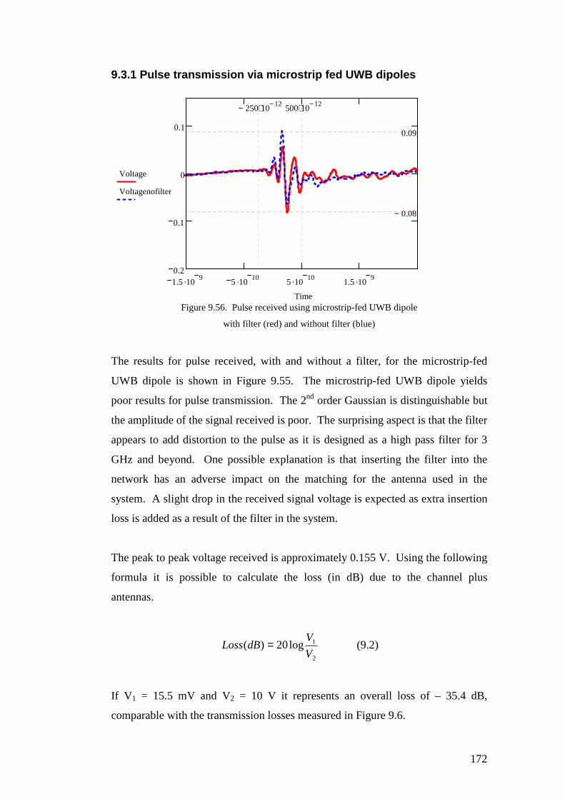
172
9.3.1 Pulse transmission via microstrip fed UWB dipoles
Figure 9.56. Pulse received using microstrip-fed UWB dipole
with filter (red) and without filter (blue)
The results for pulse received, with and without a filter, for the microstrip-fed
UWB dipole is shown in Figure 9.55. The microstrip-fed UWB dipole yields
poor results for pulse transmission. The 2nd order Gaussian is distinguishable but
the amplitude of the signal received is poor. The surprising aspect is that the filter
appears to add distortion to the pulse as it is designed as a high pass filter for 3
GHz and beyond. One possible explanation is that inserting the filter into the
network has an adverse impact on the matching for the antenna used in the
system. A slight drop in the received signal voltage is expected as extra insertion
loss is added as a result of the filter in the system.
The peak to peak voltage received is approximately 0.155 V. Using the following
formula it is possible to calculate the loss (in dB) due to the channel plus
antennas.
2
1log20)(V
VdBLoss = (9.2)
If V 1 = 15.5 mV and V2 = 10 V it represents an overall loss of – 35.4 dB,
comparable with the transmission losses measured in Figure 9.6.
1.5.109
5 .1010
5 .1010
1.5.109
0.2
0.1
0
0.1
0.08−
0.09
Voltage
Voltagenofilter
250− 1012−⋅ 500 10
12−⋅
Time

173
To the authors knowledge there is currently no method used to quantify received
pulse quality with respect to distortion. The following method is proposed to give
a quick insight into the quality. Ideally the pulse should arrive with no distortion,
which means a completely flat response after the pulse. In the case of Figure 9.54
the response should be flat after 500ps i.e. a zero voltage level. A relationship
between the peak-to-peak voltage of the pulse and the distortion after it is defined
as:
)(
)()(
pk
pk
VvoltagePulse
pulseafterVdistortionMaxDFFactorDistortion = (9.3)
Equation 9.3 implies that distortion factor will be zero if there is no distortion
after the pulse. It is also useful to quantify the amount of noise relative to the
amplitude of the received pulse. Values for distortion factor were calculated for
the pulses in Figure 9.53.
With filter:
21.014.0
03.0 ==DF
Without filter:
16.0155.0
033.0 ==DF
Analysing the results for distortion factor it is clear that the microstrip-fed UWB
dipole performs better without the filter.
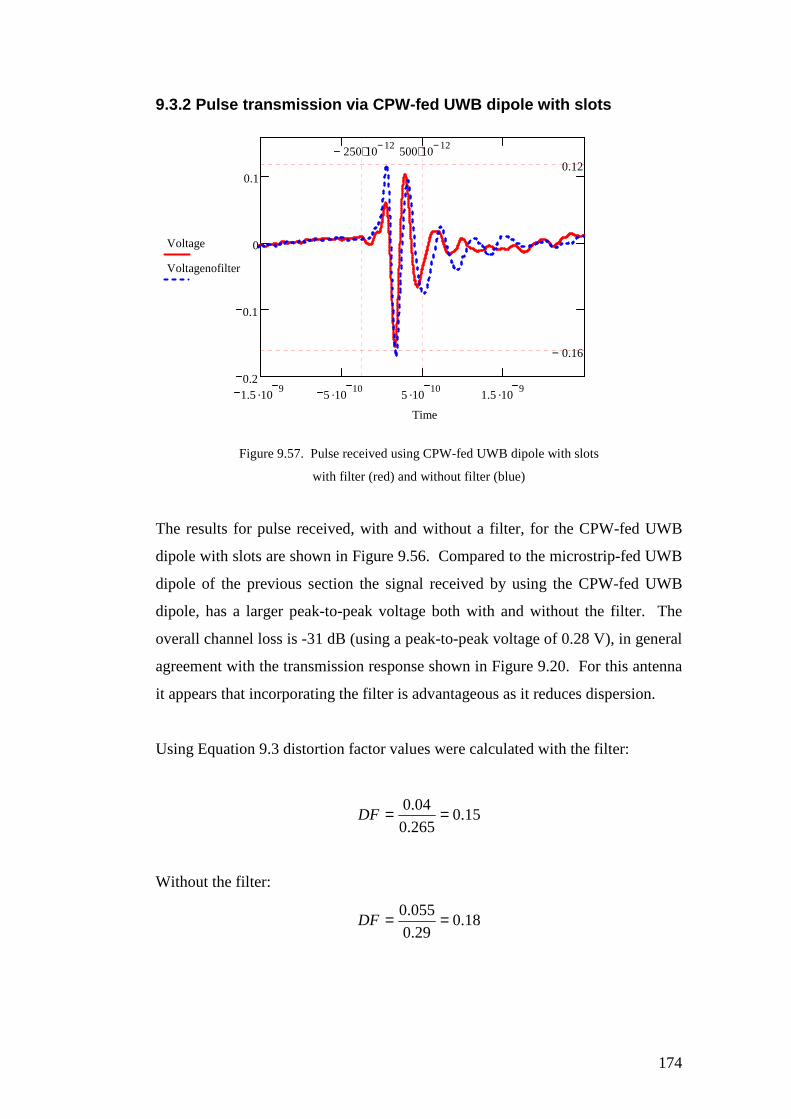
174
9.3.2 Pulse transmission via CPW-fed UWB dipole with slots
Figure 9.57. Pulse received using CPW-fed UWB dipole with slots
with filter (red) and without filter (blue)
The results for pulse received, with and without a filter, for the CPW-fed UWB
dipole with slots are shown in Figure 9.56. Compared to the microstrip-fed UWB
dipole of the previous section the signal received by using the CPW-fed UWB
dipole, has a larger peak-to-peak voltage both with and without the filter. The
overall channel loss is -31 dB (using a peak-to-peak voltage of 0.28 V), in general
agreement with the transmission response shown in Figure 9.20. For this antenna
it appears that incorporating the filter is advantageous as it reduces dispersion.
Using Equation 9.3 distortion factor values were calculated with the filter:
15.0265.0
04.0 ==DF
Without the filter:
18.029.0
055.0 ==DF
1.5.109
5 .1010
5 .1010
1.5.109
0.2
0.1
0
0.1
0.16−
0.12
Voltage
Voltagenofilter
250− 1012−⋅ 500 10
12−⋅
Time

175
Analysing these value they correspond to Figure 9.55 that the pulse with the filter
has less distortion. Also the pulse received using the filter plus the CPW-fed
UWB dipole performs better than the pulse received by microstrip-fed UWB
dipole.
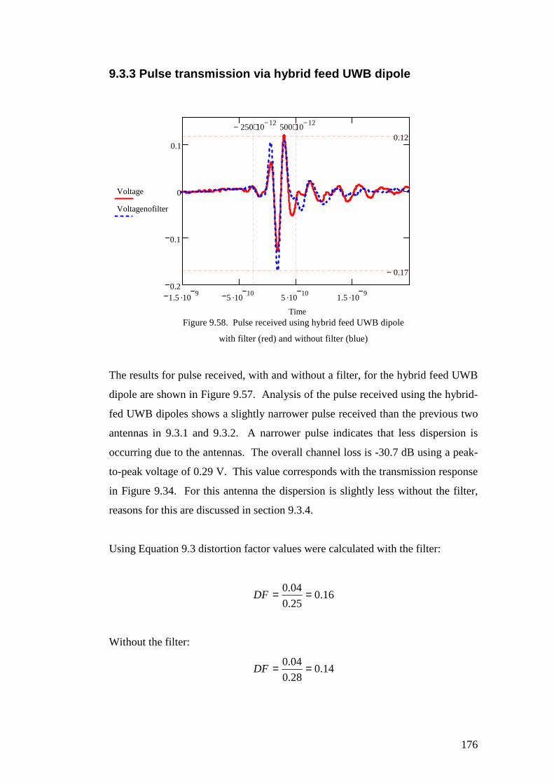
176
9.3.3 Pulse transmission via hybrid feed UWB dipole
Figure 9.58. Pulse received using hybrid feed UWB dipole
with filter (red) and without filter (blue)
The results for pulse received, with and without a filter, for the hybrid feed UWB
dipole are shown in Figure 9.57. Analysis of the pulse received using the hybrid-
fed UWB dipoles shows a slightly narrower pulse received than the previous two
antennas in 9.3.1 and 9.3.2. A narrower pulse indicates that less dispersion is
occurring due to the antennas. The overall channel loss is -30.7 dB using a peak-
to-peak voltage of 0.29 V. This value corresponds with the transmission response
in Figure 9.34. For this antenna the dispersion is slightly less without the filter,
reasons for this are discussed in section 9.3.4.
Using Equation 9.3 distortion factor values were calculated with the filter:
16.025.0
04.0 ==DF
Without the filter:
14.028.0
04.0 ==DF
1.5.109
5 .1010
5 .1010
1.5.109
0.2
0.1
0
0.1
0.17−
0.12
Voltage
Voltagenofilter
250− 1012−⋅ 500 10
12−⋅
Time

177
These values suggest that the pulse without the filter has slightly less distortion.
While there is not much difference between the distortion factor values,
inspection of Figure 9.57 shows the distortion on the pulse without the filter tends
to zero after 1.5 ns, while the pulse with the filter still has distortion present.
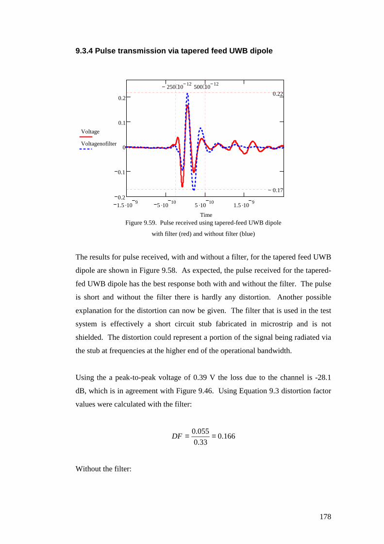
178
9.3.4 Pulse transmission via tapered feed UWB dipole
Figure 9.59. Pulse received using tapered-feed UWB dipole
with filter (red) and without filter (blue)
The results for pulse received, with and without a filter, for the tapered feed UWB
dipole are shown in Figure 9.58. As expected, the pulse received for the tapered-
fed UWB dipole has the best response both with and without the filter. The pulse
is short and without the filter there is hardly any distortion. Another possible
explanation for the distortion can now be given. The filter that is used in the test
system is effectively a short circuit stub fabricated in microstrip and is not
shielded. The distortion could represent a portion of the signal being radiated via
the stub at frequencies at the higher end of the operational bandwidth.
Using the a peak-to-peak voltage of 0.39 V the loss due to the channel is -28.1
dB, which is in agreement with Figure 9.46. Using Equation 9.3 distortion factor
values were calculated with the filter:
166.033.0
055.0 ==DF
Without the filter:
1.5.109
5 .1010
5 .1010
1.5.109
0.2
0.1
0
0.1
0.2
0.17−
0.22
Voltage
Voltagenofilter
250− 1012−⋅ 500 10
12−⋅
Time

179
081.0395.0
032.0 ==DF
The difference between the distortion factor values highlights the impact of the
filter in adding distortion.

180
9.4 Evaluation of UWB dipoles
This section compares appropriate performance metrics of the various antennas
discussed in this chapter. As all antennas have similar simulated radiation
patterns and group delay results these parameters are omitted from table 9.1.
Antenna Micrsostrip-fed
UWB dipole
with slots
CPW-fed UWB
dipole with slots
Hybrid-fed UWB
dipole
Tapered feed
UWB dipole
Operates over
bandwidth (3.16-
10.16 GHz)
No
Yes
Yes
Yes
Leakage Current Yes Yes Yes No
Size Small Small Medium Large
DF with filter 0.21 0.15 0.16 0.166
DF without filter 0.16 0.18 0.14 0.081
Signal Loss (dB) -35.4 -31 -30.7 -28.1
Table 9.1. Performance comparison of UWB dipoles
It is clear from table 9.1 and all the previous work in this chapter that the tapered
feed UWB dipole has the best characteristics for operation in a UWB channel
modelling experiment. The only drawback is the size and ease of integration into
a integrated circuit due to the complex feeding arrangement. If the feeding
arrangement for Hybrid-fed UWB dipole was extended then it would likely give a
similar performance to that of the tapered feed UWB dipole. It would also have
the advantage of having the null of the far-field radiation pattern positioned so
that the feed cable sits in the null for the majority of operational bandwidth.
Though from pulse transmission experiment, which is only line of sight, it appears
this does not matter.
This chapter concludes the research carried out on suitable UWB antennas for
wireless sensor network applications. The following chapter investigates
narrowband transceiver architectures and suitable antennas.

181
10. Narrowband Antenna Design
This chapter discusses the design work carried out in direct relation to the
Speckled Computing Consortiums objective of designing a 5mm3 ‘Speck’.
Antennas discussed in this chapter are designed at the 2.4 GHz and 5.8 GHz ISM
bands. To give an understanding of frequencies chosen the next section discusses
the radio architectures investigated during this project.
10.1 Narrowband Radio Architectures
As discussed in chapter 1, for the autonomous wireless sensors of the Speckled
Computing Consortium strict requirements are placed on the RF-front end.
Perhaps the most challenging is low power consumption (less than 400uW). As
the power requirements for conventional narrowband systems far exceeded the
power budget for the RF front-end a lower power system was investigated. The
design chosen removed the power consuming mixers, and simplified the topology.
The architecture chosen was based on incoherent diode detection, and is discussed
in the next section.
In combination with a super regenerative detector receiver, a further reduction in
the power consumption was obtained. This architecture is outlined in section
10.1.1.
10.1.1 Diode rectifier
One way to reduce power consumption is to use a simple modulation scheme such
as On-Off Keying (OOK), as this facilitates the design of very simple circuits
with small numbers of active devices. Figure 10.1 shows the layout of a diode
rectifier circuit which comprises of a directly modulated oscillator and antenna on
the transmit (TX) side. The receive (RX) side comprises of an antenna, a low
noise amplifier and an envelope detector. It was found that it was necessary to
insert an amplifier at the Rx side to get a usable signal level.
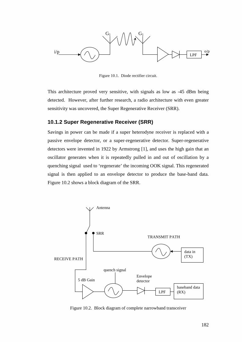
182
Figure 10.1. Diode rectifier circuit.
This architecture proved very sensitive, with signals as low as -45 dBm being
detected. However, after further research, a radio architecture with even greater
sensitivity was uncovered, the Super Regenerative Receiver (SRR).
10.1.2 Super Regenerative Receiver (SRR)
Savings in power can be made if a super heterodyne receiver is replaced with a
passive envelope detector, or a super-regenerative detector. Super-regenerative
detectors were invented in 1922 by Armstrong [1], and uses the high gain that an
oscillator generates when it is repeatedly pulled in and out of oscillation by a
quenching signal used to ‘regenerate’ the incoming OOK signal. This regenerated
signal is then applied to an envelope detector to produce the base-band data.
Figure 10.2 shows a block diagram of the SRR.
Figure 10.2. Block diagram of complete narrowband transceiver
data in (TX)
quench signal
baseband data (RX) LPF
5 dB Gain
Antenna
Envelope detector
TRANSMIT PATH
RECEIVE PATH
SRR
G1 G1
i/p LPF
o/p

183
The receiver consists of a low noise, low gain (5dB) amplifier, a super-
regenerative oscillator, and passive envelope detector, which includes a second-
order low-pass filter. The amplifier isolates the super-regenerative oscillator
signal from the antenna and hence prevents transmission during reception. The
amplified OOK signal is applied to the gate of the oscillator along with the
quenching signal but this time through the biasing circuit. The regenerated signal
is then detected and processed at baseband.
The super-regenerative architecture ensures large output voltages for small input
powers but also introduces noise to the signal. These noise levels are acceptable
however, as the SRR enables work to be carried out within the stringent power
budget of 400 µw. Shown in Figure 10.3 is a comparison of the output voltage
for both diode rectifier circuit and the SRR as a function of input signal power,
published by I. Mcgregor [2].
Figure 10.3. Output voltage vs. Input power for diode rectifier and SRR
10.1.3 Comparison of SRR link budgets at varying frequencies
This section illustrates the impact of the frequency on the power-link budget. The
two architectures that are covered in this section are the diode rectifier and the
-60 -55 -50 -45 -40 -35 -30 -25 0
2
4
6
8
10
12
14
16
18
20
5dB gain +Detector
Vo(mV)
Pin(dBm)
SRR noise
Super Regenerative Receiver

184
SRR. Three antennas (rectaxial, folded dipole and pseudo patch) are used in this
comparison at representative frequencies of operation
The power-link budget is calculated by using collected data from simulated and
experimental results. The Friis equation is given for power and power in dBm by
Equations 10.1 and 10.2. A block diagram showing the parameters used to
calculate the free space loss is shown in Figure 10.4.
tr PGGR
P 21
2
4
=
πλ
(10.1)
= −3)( 10110
x
PLogP r
dBmr (10.2)
Figure 10.4 Basic block diagram illustrating Friis equation.
The Friis transmission equation is defined by Balanis [3]. It relates the power
delivered to the receiver (Pr) to the input power of the transmitting antenna (Pt)
between two antennas separated by a distance, R, greater than λ/2 2D where D is
the maximum linear dimension of the antenna. The term (λ/4πR)2 is known as the
free-space loss factor and accounts for the spherical spreading of energy by the
antenna. For example, at 2.45 GHz, λ=0.1224 m and if both antennas are
considered to be isotropic radiators (i.e. gain of 1), with a separation of R = 0.1m,
and input power of 0 dBm (1mW), then the output power will be -40 dBm (0.1
µW). This means that there is a -20 dB loss in the channel. It is important to
remember that this only occurs if the antennas are pointing directly at each other
and there is no polarisation mismatch.
Pt Pr
R
G1 G2
λ

185
To calculate the power link budget known values of gain, and output powers are
combined with the Friis equation to create a table including all the losses and
gains. The target power consumption for the system is to be less than 400 µW (-4
dBm). Shown in tables 10.1, 10.2 and 10.3 are approximate link budgets for a 10
cm distance between transceivers at 2.45 GHz and 5.8 GHz. The values for
antenna gain in table 10.1 are measured, while those in tables 10.2 and 10.3 are
simulated values. It is assumed that the characteristic impedance of the system is
50Ω. The antennas given in tables 10.2 and 10.3 are discussed in Sections 10.2
and 10.3 respectively.
Frequency = 2.45 GHz; R = 0.1 m; Antenna Type: Rectaxial
Oscillator Antenna(Tx) Channel Loss Antenna(Rx) Amplifier
-10.85dBm 2.2dBi -20 dB 2.2dBi 5 dB
Received Power Output Voltage (rms)
-21.45 dBm 20 mV
Table 10.1 Power link budget for 2.45 GHz
Frequency = 5.8 GHz; R = 0.1 m; Antenna Type: Folded dipole over ground
Oscillator Antenna(Tx) Channel
Loss
Antenna(Rx) Amplifier
-10.85dBm -8.6 dBi -34 dB -8.6 dBi 5 dB
Received Power Output Voltage
-57.05 dBm 0.315 mV
Table 10.2 Power link budget for 5.8 GHz
Frequency = 5.8 GHz; R = 0.1 m; Antenna Type: Pseudo patch antenna
Oscillator Antenna(Tx) Channel
Loss
Antenna(Rx) Amplifier
-10.85dBm -3.2 dBi -34 dB -3.2 dBi 5 dB
Received Power Output Voltage
-39.45 dBm 1.121 mV
Table 10.3 Power link budget for 5.8 GHz
186
All three tables are representative of both the diode rectifier method and the SRR.
While they are speculative they still illustrate the power levels involved. The
important point illustrated by Figure 10.3 is that the SRR is much more sensitive
and can detect signals down to -60 dBm.
10.2 The Rectaxial antenna
With the development of the SRR outlined in the previous section the narrowband
transceiver could now be operated at a relatively low frequency (2.45 GHz or 5.8
GHz). The rectaxial antenna was the first antenna designed in this project that
offered an electrically small size with good performance. At the time the SRR
was being developed, the focus was on the 2.4 GHz ISM band. When the SRR
became fully operational there was an attempt to move up to the next ISM licence
exempt band at 5.8 GHz. Unfortunately, the rectaxial antenna did not scale with
frequency. The reasons behind this are discussed in a later section of this chapter.
10.2.1 Background theory
The rectaxial antenna is a derivation of the helical antenna first developed by
Krauss in 1947 [4]. The helical antenna consists of a piece of conducting wire
wound into a helix and in most cases is placed either perpendicular or
asymmetrically relative to a ground plane. The helical antenna operates in two
fundamental modes the ‘axial’ mode and the ‘normal’ mode.
The ‘axial’ mode occurs when the dimensions are at, or greater than, the operating
wavelength. For 2.45 GHz operation , this corresponds to 12.24 cm. The space
between the coils and the diameter of the coils determine the antennas
wavelength. The antenna can be classed as ‘endfire’ and increasing the number of
coils increases the directivity. Another benefit of this mode is that it can generate
circular polarisation (CP) by simply using the direction of the winding to generate
left hand CP (anti-clockwise) or right hand CP (clockwise). As this class of
antenna size is comparable to its wavelength, (for CP operation the diameter
should approximately be one wavelength), there is no further discussion of the
‘axial’ mode as it is not relevant to the required geometries of the target
application.

187
In the ‘normal’ mode the helix dimensions are very small compared to
wavelength. Figure 10.5 shows a helix and the relevant parameters as described
by Krauss [5].
Where, D = diameter of helix (centre to centre)
C = circumference of helix = πD
S = spacing between turns (centre to centre)
α = pitch angle = arctan S/ πD
L = Length of 1 turn
n = number of turns
A = axial length = nS
d = diameter of helix conductor
Figure 10.5. (a) Helix and associated dimensions (b) Relation between circumference, spacing,
turn length, and pitch angle of a helix.
The normal radiation mode occurs when the helix is very short i.e. nL<<λ. In this
case, the current can be considered to be of uniform magnitude and phase along
the entire helix. Using the helix described by Krauss [6] as shown in Figure 10.6
(a) the maximum radiation in this case is normal to the helix axis and there is zero
field in the direction of the z-axis.

188
Figure 10.6. Dimensions and coordinates for (a) helix (b) loop and (c) dipole.
(d) Helix as a succession of loops and dipoles (e) Helix for normal mode calculations
When the pitch angle is zero, the helix can be considered to be a loop, as shown
by Figure 10.6 (b). When the pitch angle is ninety degrees, the helix straightens
out and becomes straight wire, as shown by Figure 10.6 (c). These two cases are
the limits of the helix and can be used to calculate the radiation patterns.
Essentially a helical antenna operating in the normal mode can be analysed as a
series of small loops and short dipoles connected in series. For the helix to be
analysed using this approximation it has to satisfy the criteria of D ≈ 0.1λ and S ≈
0.05λ.
As the current magnitude and phase are uniform over the helix, the far-field
patterns are independent of the number of turns. As a result, the far-field patterns
can be calculated by using the field patterns of a small loop antenna and an
infinitesimal dipole. The far-field of a small loop only has a φE component. Its
value is given by [7].
2
2 sin][120
λθπ
φA
r
IE = (10.3)
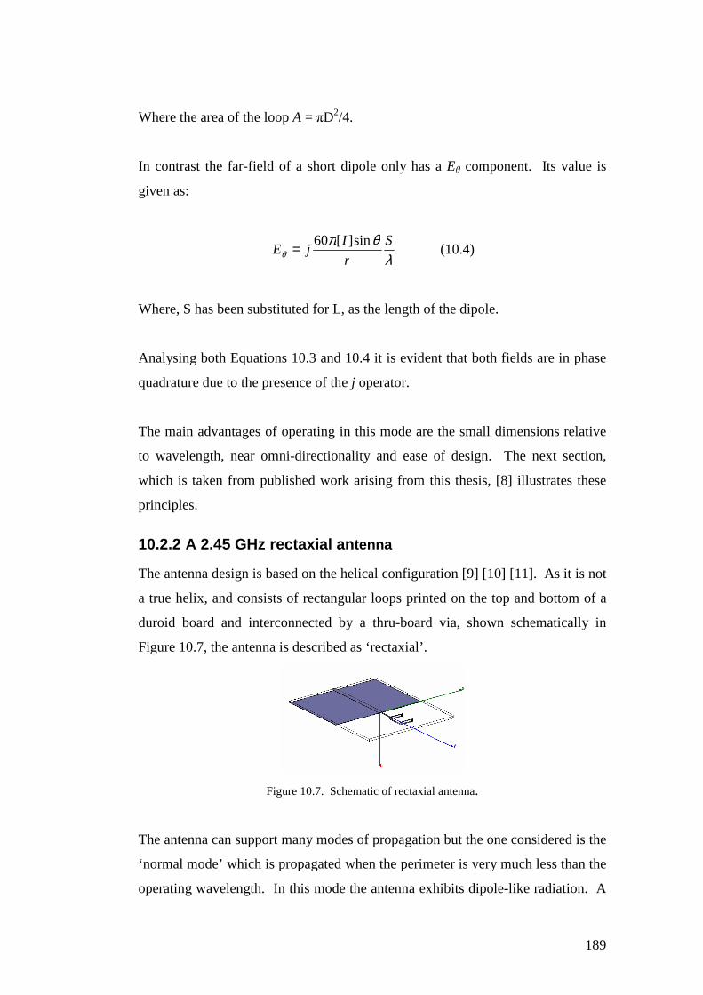
189
Where the area of the loop A = πD2/4.
In contrast the far-field of a short dipole only has a Eθ component. Its value is
given as:
λθπ
θS
r
IjE
sin][60= (10.4)
Where, S has been substituted for L, as the length of the dipole.
Analysing both Equations 10.3 and 10.4 it is evident that both fields are in phase
quadrature due to the presence of the j operator.
The main advantages of operating in this mode are the small dimensions relative
to wavelength, near omni-directionality and ease of design. The next section,
which is taken from published work arising from this thesis, [8] illustrates these
principles.
10.2.2 A 2.45 GHz rectaxial antenna
The antenna design is based on the helical configuration [9] [10] [11]. As it is not
a true helix, and consists of rectangular loops printed on the top and bottom of a
duroid board and interconnected by a thru-board via, shown schematically in
Figure 10.7, the antenna is described as ‘rectaxial’.
Figure 10.7. Schematic of rectaxial antenna.
The antenna can support many modes of propagation but the one considered is the
‘normal mode’ which is propagated when the perimeter is very much less than the
operating wavelength. In this mode the antenna exhibits dipole-like radiation. A
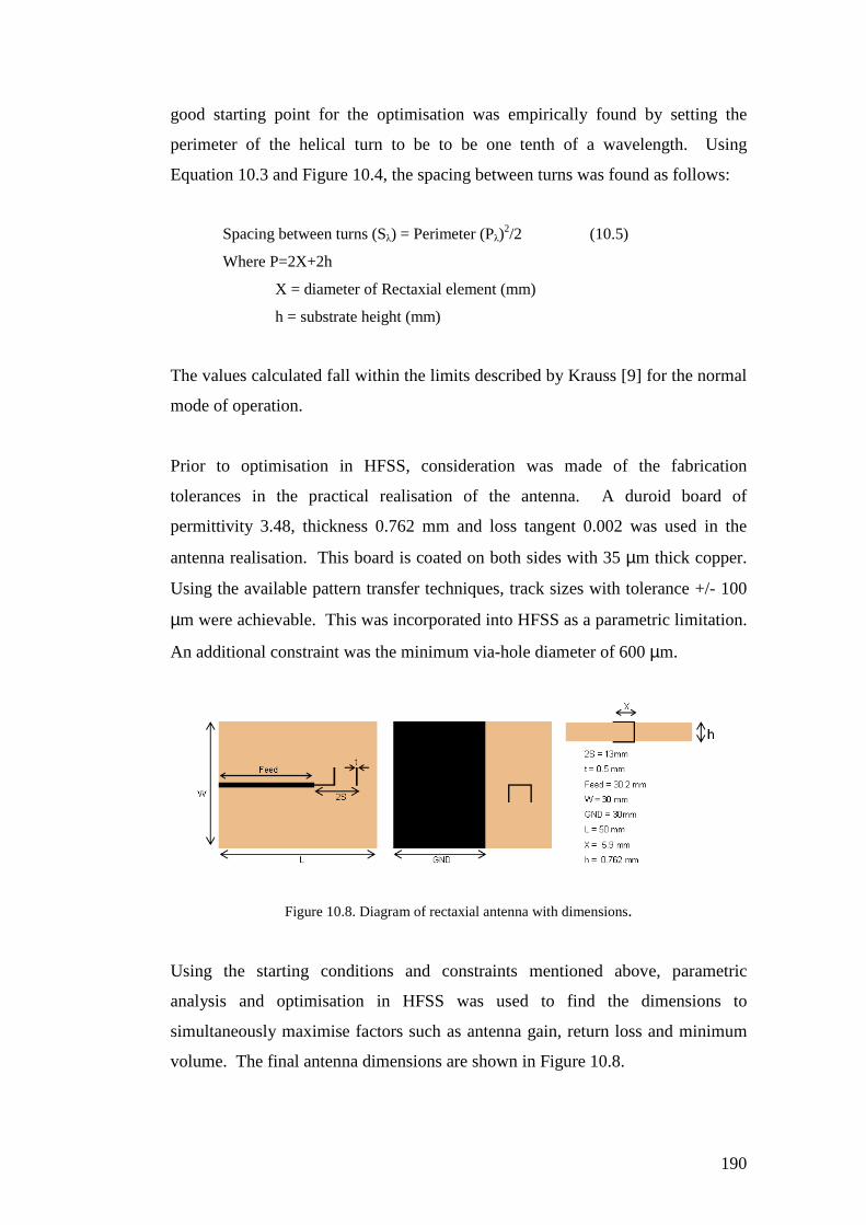
190
good starting point for the optimisation was empirically found by setting the
perimeter of the helical turn to be to be one tenth of a wavelength. Using
Equation 10.3 and Figure 10.4, the spacing between turns was found as follows:
Spacing between turns (Sλ) = Perimeter (Pλ)2/2 (10.5)
Where P=2X+2h
X = diameter of Rectaxial element (mm)
h = substrate height (mm)
The values calculated fall within the limits described by Krauss [9] for the normal
mode of operation.
Prior to optimisation in HFSS, consideration was made of the fabrication
tolerances in the practical realisation of the antenna. A duroid board of
permittivity 3.48, thickness 0.762 mm and loss tangent 0.002 was used in the
antenna realisation. This board is coated on both sides with 35 µm thick copper.
Using the available pattern transfer techniques, track sizes with tolerance +/- 100
µm were achievable. This was incorporated into HFSS as a parametric limitation.
An additional constraint was the minimum via-hole diameter of 600 µm.
Figure 10.8. Diagram of rectaxial antenna with dimensions.
Using the starting conditions and constraints mentioned above, parametric
analysis and optimisation in HFSS was used to find the dimensions to
simultaneously maximise factors such as antenna gain, return loss and minimum
volume. The final antenna dimensions are shown in Figure 10.8.
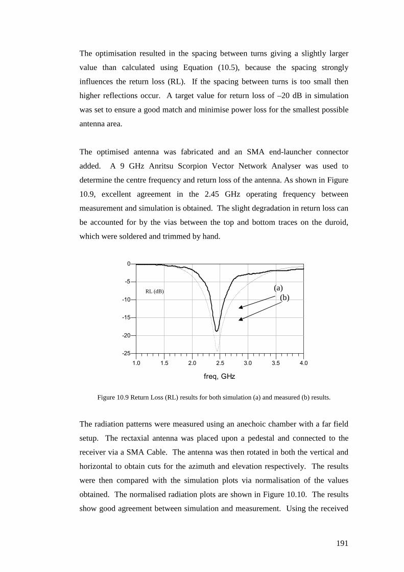
191
The optimisation resulted in the spacing between turns giving a slightly larger
value than calculated using Equation (10.5), because the spacing strongly
influences the return loss (RL). If the spacing between turns is too small then
higher reflections occur. A target value for return loss of –20 dB in simulation
was set to ensure a good match and minimise power loss for the smallest possible
antenna area.
The optimised antenna was fabricated and an SMA end-launcher connector
added. A 9 GHz Anritsu Scorpion Vector Network Analyser was used to
determine the centre frequency and return loss of the antenna. As shown in Figure
10.9, excellent agreement in the 2.45 GHz operating frequency between
measurement and simulation is obtained. The slight degradation in return loss can
be accounted for by the vias between the top and bottom traces on the duroid,
which were soldered and trimmed by hand.
1.5 2.0 2.5 3.0 3.51.0 4.0
-20
-15
-10
-5
-25
0
freq, GHz
Figure 10.9 Return Loss (RL) results for both simulation (a) and measured (b) results.
The radiation patterns were measured using an anechoic chamber with a far field
setup. The rectaxial antenna was placed upon a pedestal and connected to the
receiver via a SMA Cable. The antenna was then rotated in both the vertical and
horizontal to obtain cuts for the azimuth and elevation respectively. The results
were then compared with the simulation plots via normalisation of the values
obtained. The normalised radiation plots are shown in Figure 10.10. The results
show good agreement between simulation and measurement. Using the received
(b) (a) RL (dB)

192
power level from a dipole as a reference, an average gain of 2.2 dBi was obtained
with a peak gain of 2.69 dBi along the boresight.
Measured Elevation
Measured Azimuth
Simulated Azimuth
Simulated Elevation
-10 1-5
Figure 10.10. Normalised radiation patterns obtained by both simulation and measurement.
10.2.3 Design of 5.8 GHz rectaxial antenna
After the previous antenna had been designed and fabricated and appeared to
operate well, it was decided to investigate its performance at a higher frequency.
5.8 GHz was chosen as it is a licence exempt band [12]. Using the design
equations outlined in the previous section a model was created using HFSS that
resonated at 5.8 GHz. A schematic of the model is shown below in Figure 10.11.
Figure 10.11. Schematic of 5.8 GHz rectaxial antenna
180o
270o
0o
90o
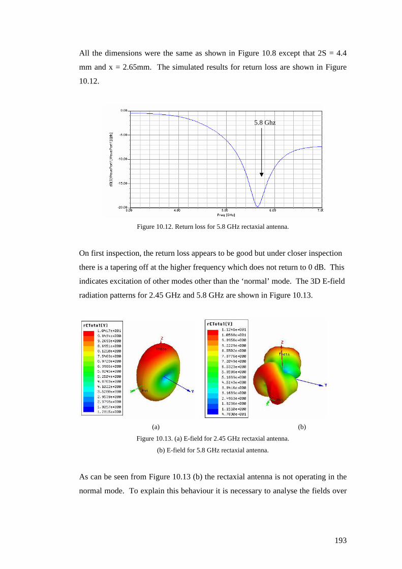
193
All the dimensions were the same as shown in Figure 10.8 except that 2S = 4.4
mm and x = 2.65mm. The simulated results for return loss are shown in Figure
10.12.
Figure 10.12. Return loss for 5.8 GHz rectaxial antenna.
On first inspection, the return loss appears to be good but under closer inspection
there is a tapering off at the higher frequency which does not return to 0 dB. This
indicates excitation of other modes other than the ‘normal’ mode. The 3D E-field
radiation patterns for 2.45 GHz and 5.8 GHz are shown in Figure 10.13.
(a) (b)
Figure 10.13. (a) E-field for 2.45 GHz rectaxial antenna.
(b) E-field for 5.8 GHz rectaxial antenna.
As can be seen from Figure 10.13 (b) the rectaxial antenna is not operating in the
normal mode. To explain this behaviour it is necessary to analyse the fields over
5.8 Ghz
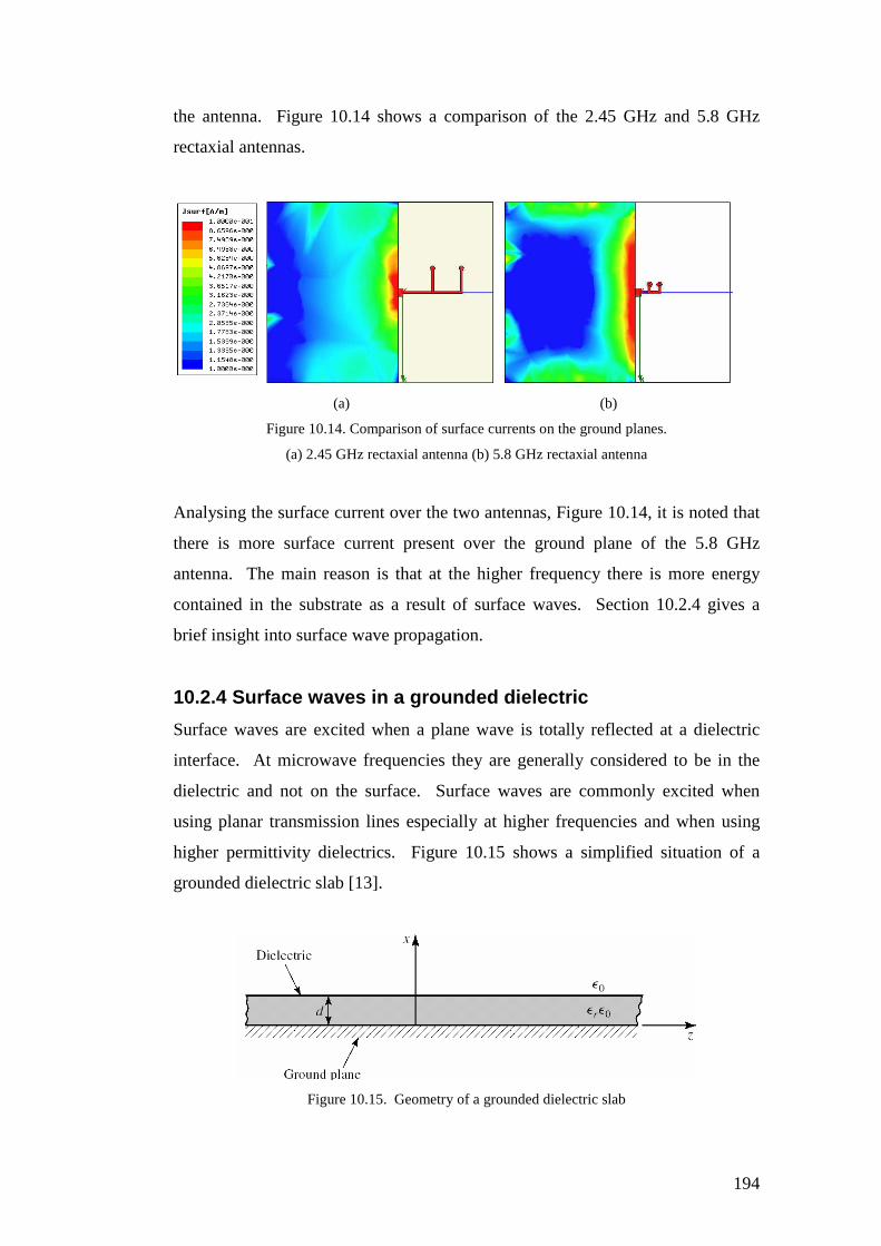
194
the antenna. Figure 10.14 shows a comparison of the 2.45 GHz and 5.8 GHz
rectaxial antennas.
(a) (b)
Figure 10.14. Comparison of surface currents on the ground planes.
(a) 2.45 GHz rectaxial antenna (b) 5.8 GHz rectaxial antenna
Analysing the surface current over the two antennas, Figure 10.14, it is noted that
there is more surface current present over the ground plane of the 5.8 GHz
antenna. The main reason is that at the higher frequency there is more energy
contained in the substrate as a result of surface waves. Section 10.2.4 gives a
brief insight into surface wave propagation.
10.2.4 Surface waves in a grounded dielectric
Surface waves are excited when a plane wave is totally reflected at a dielectric
interface. At microwave frequencies they are generally considered to be in the
dielectric and not on the surface. Surface waves are commonly excited when
using planar transmission lines especially at higher frequencies and when using
higher permittivity dielectrics. Figure 10.15 shows a simplified situation of a
grounded dielectric slab [13].
Figure 10.15. Geometry of a grounded dielectric slab

195
The dielectric slab has a thickness d and a dielectric constant of εr. For any
dielectric slab of nonzero thickness and a permittivity greater than unity, there is
one mode that can always propagate within the substrate. The mode is transverse
magnetic and is known as the TM0 mode. This mode has a zero cut-off frequency
and propagation is assumed to be in the z direction and has a e-jβz propagation
factor. We are not concerned with the higher order TM modes or any of the TE
modes as they all occur at much higher frequencies. The cut-off frequencies for
both TM and TE modes are given by Pozar[14]. The TM modes are given by:
12 −=
r
cd
ncf
ε, n = 0,1,2,… (10.6)
For the TE modes:
14
)12(
−−=
r
cd
cnf
ε, n = 1,2,3,… (10.7)
As the frequency increases with a constant substrate height the substrate becomes
electrically larger allowing more energy to be propagated as surface wave mode
within the substrate. The next section applies this knowledge to the problems
associated with the 5.8 GHz rectaxial antenna.
10.2.5 Field analysis of 5.8 GHz Rectaxial antenna
Surface waves are launched via any type of discontinuity from planar
transmission lines. In the case of the rectaxial antenna, the surface wave is
launched at the interface between the feed and the antenna. To verify this, HFSS
was used plot the electric field vector at the interface. This is shown in Figure
10.16.
Figure 10.16 E-field vector plot of substrate
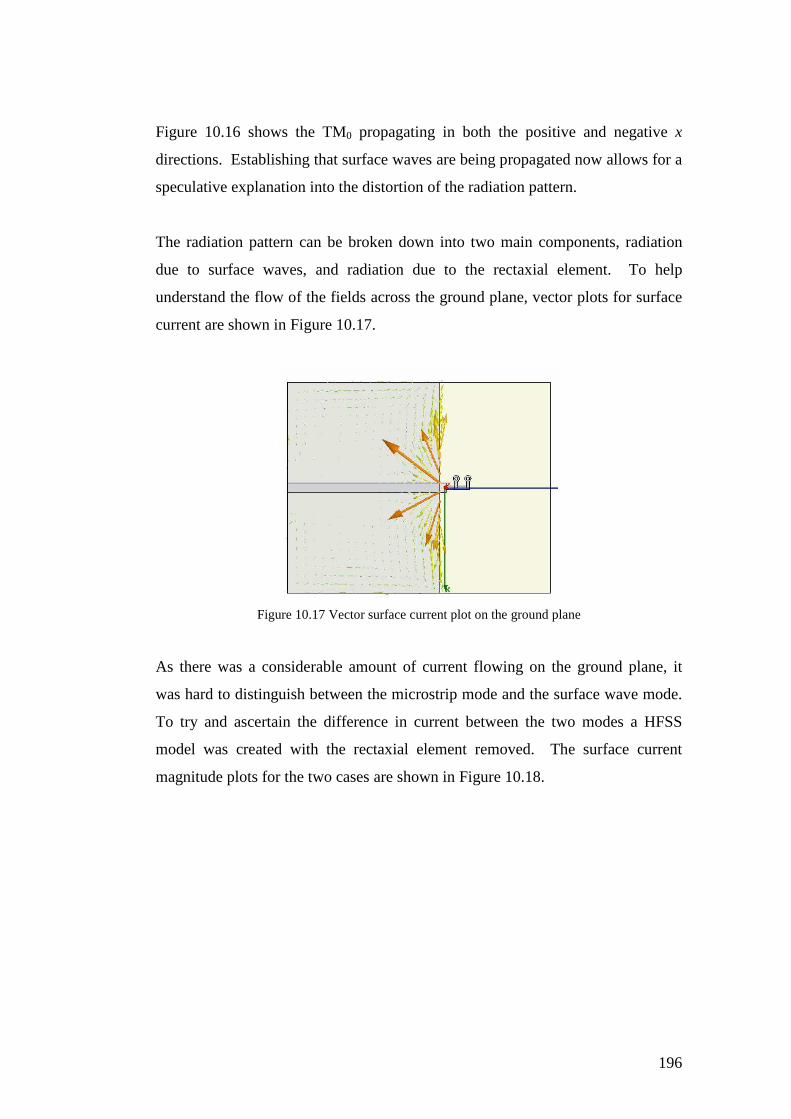
196
Figure 10.16 shows the TM0 propagating in both the positive and negative x
directions. Establishing that surface waves are being propagated now allows for a
speculative explanation into the distortion of the radiation pattern.
The radiation pattern can be broken down into two main components, radiation
due to surface waves, and radiation due to the rectaxial element. To help
understand the flow of the fields across the ground plane, vector plots for surface
current are shown in Figure 10.17.
Figure 10.17 Vector surface current plot on the ground plane
As there was a considerable amount of current flowing on the ground plane, it
was hard to distinguish between the microstrip mode and the surface wave mode.
To try and ascertain the difference in current between the two modes a HFSS
model was created with the rectaxial element removed. The surface current
magnitude plots for the two cases are shown in Figure 10.18.

197
(a)
(b)
Figure 10.18. Surface current plot (a) with and (b) without rectaxial element
The plots in Figure 10.18 both have the same scale for surface current magnitude.
Figure 10.18 (a) has a peak current maximum of approximately 100 A/m, while
the model with no antenna, Figure 10.18 (b), has the peak current value of about 4
A/m. While this is much lower, there is still propagation of waves into free space.
The electric field and gain far-field radiation patterns from the HFSS model with
no antenna, are shown in Figure 10.19.

198
(a)
(b)
0
90
180
270
3
2
1
noantennaradius
noantennaθ deg⋅
(c)
Figure 10.19. Simulated plots for (a) 3D E-field (b) 3D Gain (dBi) (c) x-y cut of E-field
The main radiation mechanism for the board with no antenna is when the current,
which is being driven from the stub, meets the corner. This is highlighted by
Figure 10.19 (a), which shows two prominent peaks in the y direction. To
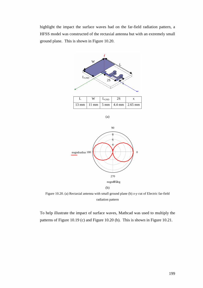
199
highlight the impact the surface waves had on the far-field radiation pattern, a
HFSS model was constructed of the rectaxial antenna but with an extremely small
ground plane. This is shown in Figure 10.20.
L W LGND 2S x
13 mm 11 mm 5 mm 4.4 mm 2.65 mm
(a)
0
90
180
270
8
6
4
2nogndradius
nogndθ deg⋅
(b)
Figure 10.20. (a) Rectaxial antenna with small ground plane (b) x-y cut of Electric far-field
radiation pattern
To help illustrate the impact of surface waves, Mathcad was used to multiply the
patterns of Figure 10.19 (c) and Figure 10.20 (b). This is shown in Figure 10.21.
2S x
L
LGND
W
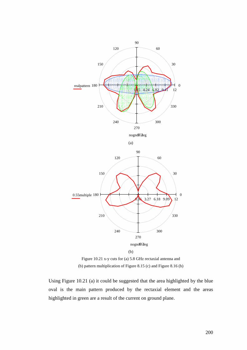
200
0
30
60
90
120
150
180
210
240
270
300
330
129.416.824.241.65realpattern
nogndθ deg⋅
(a)
0
30
60
90
120
150
180
210
240
270
300
330
129.096.183.270.360.55multiple
nogndθ deg⋅
(b)
Figure 10.21 x-y cuts for (a) 5.8 GHz rectaxial antenna and
(b) pattern multiplication of Figure 8.15 (c) and Figure 8.16 (b)
Using Figure 10.21 (a) it could be suggested that the area highlighted by the blue
oval is the main pattern produced by the rectaxial element and the areas
highlighted in green are a result of the current on ground plane.

201
Unfortunately, as a result of surface wave propagation degrading the radiation
pattern at 5.8 GHz, coupled with need for an even smaller antenna to
accommodate active circuitry, within the specification set out by the Speckled
Computing Consortium, the rectaxial antenna was deemed unsuitable. Other
antennas were therefore investigated as described next.
10.3 Integrated antennas at 5.8 GHz
After identifying the limitations of the rectaxial antenna in the previous section,
other antennas were investigated for their potential to fulfil the Specknet
requirements. These antennas where designed with the intention of taking up as
little space as possible and were designed around the MMIC transceiver circuitry,
designed by Ian McGregor and shown in Figure 10.22.
L W
6.2 mm 2.25 mm
Figure 10.22. A 5.8 GHz MMIC Transceiver.
Two antennas, a compact folded dipole and a ‘patch’, that were designed to be
integrated into and around the transceiver, are discussed in this section. Also
considered in this chapter is the approach to feeding the antennas, by the use of a
CPW-to-slotline transition to achieve optimal performance. The antennas
designed were electrically small and found to be rather inefficient. To understand
L
W

202
this lack of efficiency, this section follows with a discussion on the fundamental
limits of antennas.
10.3.1 Quality factor, bandwidth and efficiency
When designing radio frequency systems it is sometimes necessary to try and
reduce the area that the device occupies. As previously mentioned, for the class
of applications being considered by the Speckled Computing Consortium, there is
a desire for the transceiver and the antenna to fit into 5mm2. There are many
ways to reduce the area that the antenna occupies, such as, folding, meandering
and bending. The use of shorting walls, pins and high dielectric constant
materials can also be used. However, using these techniques come at a cost, as
the bandwidth and efficiency are reduced.
Chapter 3 investigated the fundamental limitations of electrically small antenna as
those whose maximum dimension is less than the 1/k, where k = wave number.
This section will investigate the impact on the quality factor, Q, of losses such as
radiation, conduction (ohmic), dielectric and surface wave losses. The total
quality factor, Qt, which is influenced by these losses, can be written as [15]:
swdcradt QQQQQ
11111 +++= (10.8)
Where:
Qt = total quality factor
Qrad = quality factor due to radiation losses
Qc = quality factor due to conductive (ohmic) losses
Qd = quality factor due to dielectric losses
Qsw = quality factor due to surface waves
For very thin substrates the losses due to surface waves are very small, and can
generally be neglected, until the substrate approaches a height large enough for
propagation of the higher order modes as discussed in section 10.2.5. For very
thin substrates (d<<λ) of arbitrary shapes (including rectangular and circular),

203
approximate formulas can be used to represent the quality factors of the various
losses in 10.8. They are as follows [16]:
µσπ fdQc = (10.9)
δtan
1=dQ (10.10)
KldG
Qt
rrad /
2ωε= (10.11)
Where:
δtan = loss tangent of dielectric substrate
σ = is the conductivity associated with any metallization used
lGt / = the total conductance per unit length of the radiating aperture
∫
∫∫=
perimeter
area
dLE
dAE
K2
2
(10.12)
To help simplify he understanding an example of a rectangular patch antenna, as
described in chapter 5, can be used. For a patch antenna operating in the
dominant TM01 mode the following are given [16]:
4
LK = (10.13)
W
GlG rad
t =/ (10.14)
The Qrad described by equation 10.11 is inversely proportional to the height of the
substrate, and for very thin substrates is the dominant factor. The fractional
bandwidth of antenna is inversely proportional to the Q of an antenna. Taking
account of all losses it can be defined as:

204
tQf
f 1
0
=∆ (10.15)
Equation 10.15 can also be modified to take into account the impedance matching
at the terminals of the antenna and is described as follows:
VSWRQ
VSWR
f
f
t
1
0
−=∆ (10.16)
The fractional bandwidth is proportional to the volume, which for a rectangular
microstrip antenna at a constant resonant frequency can be expressed as:
BW α volume = area x height = length x width x height
r
r
rr εε
εεα 111 = (10.17)
For increasing height of substrate the bandwidth increases, increasing the
dielectric constant the bandwidth decreases.
Increasing the dielectric constant also has an impact on the antenna efficiency. To
help understand the impact the conduction-dielectric efficiency, η, can be used. It
is defined as a ratio of the power delivered to the radiation resistance (Rr), to the
power delivered to Rr and the loss resistance (RL), and is written as follows:
+=
rL
r
RR
Rη (10.18)
Equation 10.18 can be expressed in terms of the quality factors described in
equation 10.8 as follows:
rad
t
t
rad
Q
Q
Q
Q==
/1
/1η (10.19)
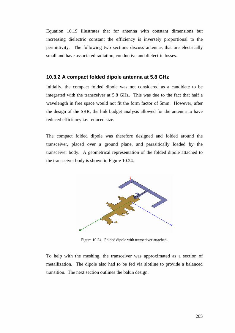
205
Equation 10.19 illustrates that for antenna with constant dimensions but
increasing dielectric constant the efficiency is inversely proportional to the
permittivity. The following two sections discuss antennas that are electrically
small and have associated radiation, conductive and dielectric losses.
10.3.2 A compact folded dipole antenna at 5.8 GHz
Initially, the compact folded dipole was not considered as a candidate to be
integrated with the transceiver at 5.8 GHz. This was due to the fact that half a
wavelength in free space would not fit the form factor of 5mm. However, after
the design of the SRR, the link budget analysis allowed for the antenna to have
reduced efficiency i.e. reduced size.
The compact folded dipole was therefore designed and folded around the
transceiver, placed over a ground plane, and parasitically loaded by the
transceiver body. A geometrical representation of the folded dipole attached to
the transceiver body is shown in Figure 10.24.
Figure 10.24. Folded dipole with transceiver attached.
To help with the meshing, the transceiver was approximated as a section of
metallization. The dipole also had to be fed via slotline to provide a balanced
transition. The next section outlines the balun design.

206
10.3.2.1 Balun design
One of the most important aspects of dipole design is ensuring that there is a
balanced feed into the centre of the dipole. For a monolithic design, this can be
provided by slotline. Unfortunately, slotline is not the transmission line of choice
when designing MMICs. More commonly, CPW or microstrip lines are used, as
they allow for easier integration between components.
The transceiver, shown in Figure 10.22, uses CPW lines to connect the discrete
components, and as a result there needs to be a transition, which acts as a balun.
A balun was designed [17], which allowed for a transition from CPW-to-slotline,
and is shown in Figure 10.25.
Figure 10.25. A CPW-to-slotline transition
As well as acting as a balun, the 50Ω CPW line to 50Ω slotline transition also
gives a certain amount of matching capability. The stub acts as a 180° phase
shifter effectively removing half the CPW mode to leave the slotline mode.
Figure 10.26 shows simulated results for S21, S11 and S22.
Stub
Slotline
CPW
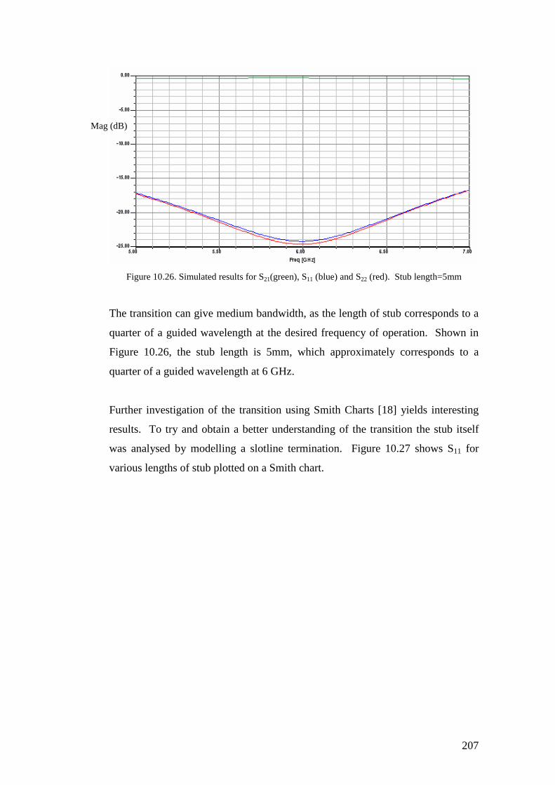
207
Figure 10.26. Simulated results for S21(green), S11 (blue) and S22 (red). Stub length=5mm
The transition can give medium bandwidth, as the length of stub corresponds to a
quarter of a guided wavelength at the desired frequency of operation. Shown in
Figure 10.26, the stub length is 5mm, which approximately corresponds to a
quarter of a guided wavelength at 6 GHz.
Further investigation of the transition using Smith Charts [18] yields interesting
results. To try and obtain a better understanding of the transition the stub itself
was analysed by modelling a slotline termination. Figure 10.27 shows S11 for
various lengths of stub plotted on a Smith chart.
Mag (dB)
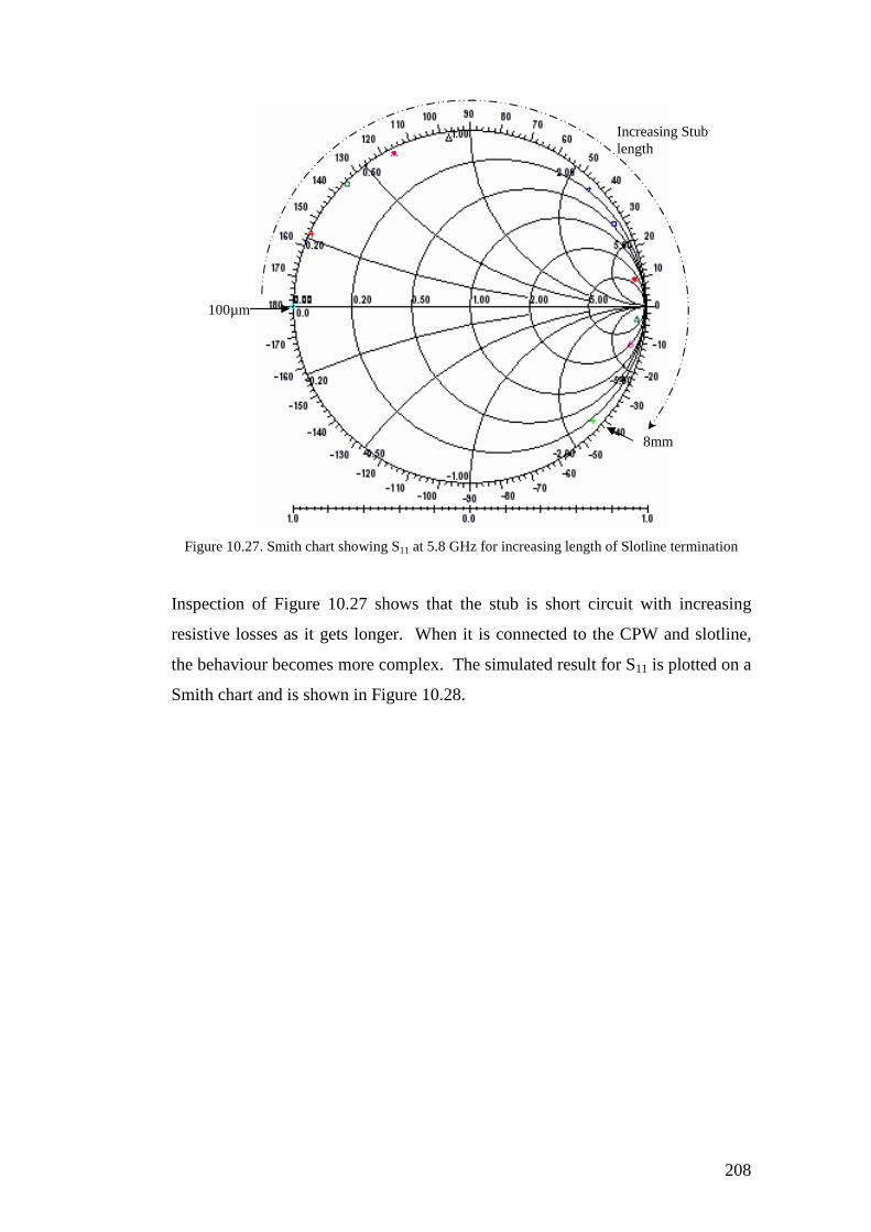
208
Figure 10.27. Smith chart showing S11 at 5.8 GHz for increasing length of Slotline termination
Inspection of Figure 10.27 shows that the stub is short circuit with increasing
resistive losses as it gets longer. When it is connected to the CPW and slotline,
the behaviour becomes more complex. The simulated result for S11 is plotted on a
Smith chart and is shown in Figure 10.28.
100µm
8mm
Increasing Stub length
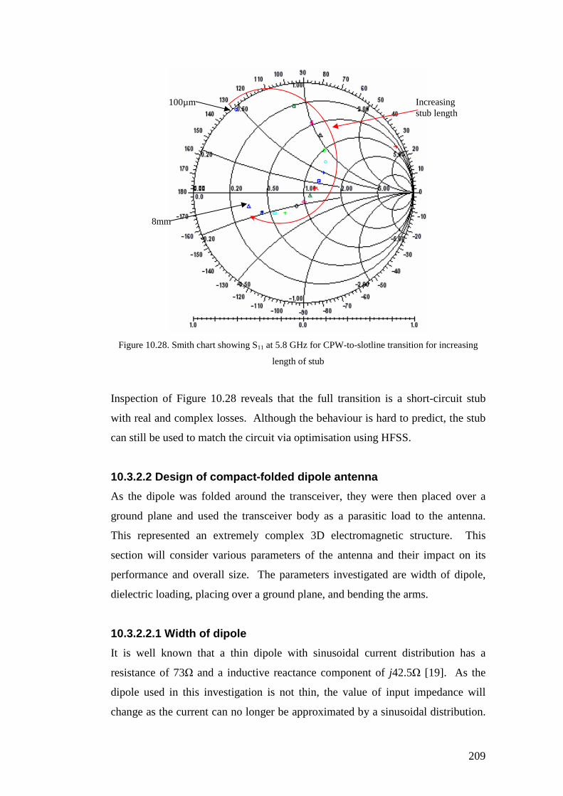
209
Figure 10.28. Smith chart showing S11 at 5.8 GHz for CPW-to-slotline transition for increasing
length of stub
Inspection of Figure 10.28 reveals that the full transition is a short-circuit stub
with real and complex losses. Although the behaviour is hard to predict, the stub
can still be used to match the circuit via optimisation using HFSS.
10.3.2.2 Design of compact-folded dipole antenna
As the dipole was folded around the transceiver, they were then placed over a
ground plane and used the transceiver body as a parasitic load to the antenna.
This represented an extremely complex 3D electromagnetic structure. This
section will consider various parameters of the antenna and their impact on its
performance and overall size. The parameters investigated are width of dipole,
dielectric loading, placing over a ground plane, and bending the arms.
10.3.2.2.1 Width of dipole
It is well known that a thin dipole with sinusoidal current distribution has a
resistance of 73Ω and a inductive reactance component of j42.5Ω [19]. As the
dipole used in this investigation is not thin, the value of input impedance will
change as the current can no longer be approximated by a sinusoidal distribution.
100µm
8mm
Increasing stub length
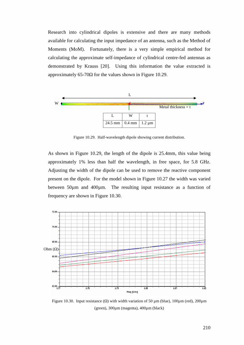
210
Research into cylindrical dipoles is extensive and there are many methods
available for calculating the input impedance of an antenna, such as the Method of
Moments (MoM). Fortunately, there is a very simple empirical method for
calculating the approximate self-impedance of cylindrical centre-fed antennas as
demonstrated by Krauss [20]. Using this information the value extracted is
approximately 65-70Ω for the values shown in Figure 10.29.
L W t
24.5 mm 0.4 mm 1.2 µm
Figure 10.29. Half-wavelength dipole showing current distribution.
As shown in Figure 10.29, the length of the dipole is 25.4mm, this value being
approximately 1% less than half the wavelength, in free space, for 5.8 GHz.
Adjusting the width of the dipole can be used to remove the reactive component
present on the dipole. For the model shown in Figure 10.27 the width was varied
between 50µm and 400µm. The resulting input resistance as a function of
frequency are shown in Figure 10.30.
Figure 10.30. Input resistance (Ω) with width variation of 50 µm (blue), 100µm (red), 200µm
(green), 300µm (magenta), 400µm (black)
L
Ohm (Ω)
W Metal thickness = t
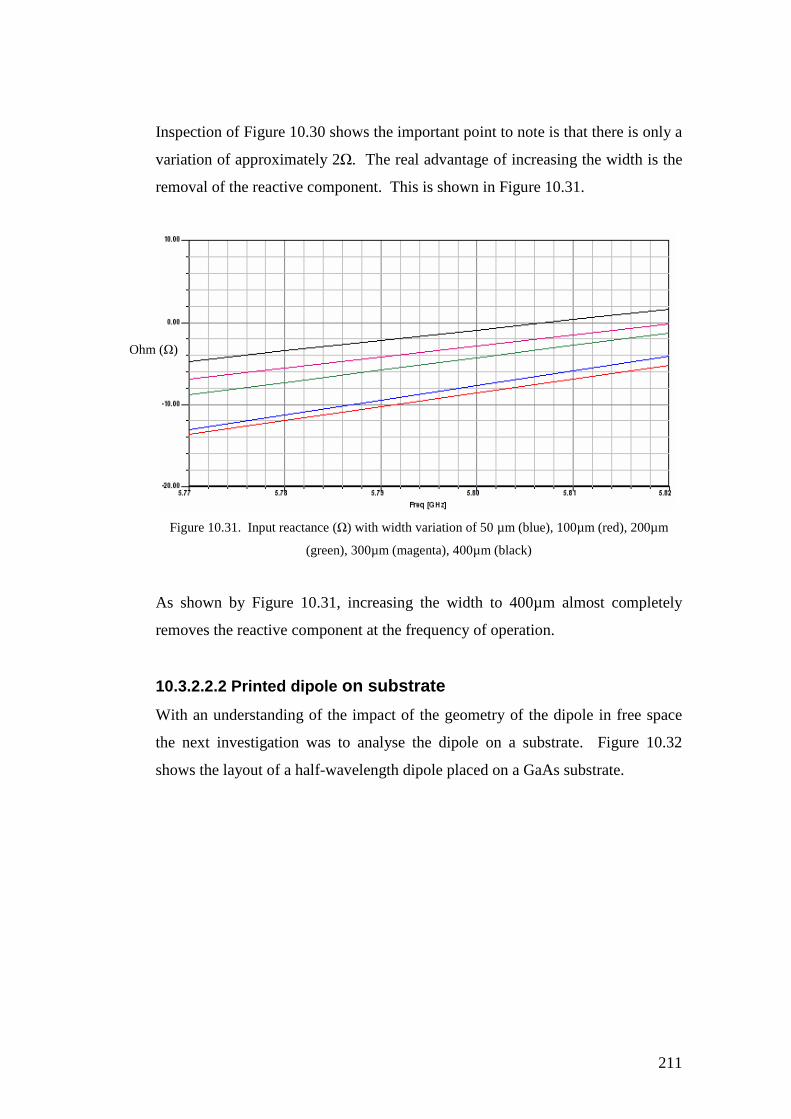
211
Inspection of Figure 10.30 shows the important point to note is that there is only a
variation of approximately 2Ω. The real advantage of increasing the width is the
removal of the reactive component. This is shown in Figure 10.31.
Figure 10.31. Input reactance (Ω) with width variation of 50 µm (blue), 100µm (red), 200µm
(green), 300µm (magenta), 400µm (black)
As shown by Figure 10.31, increasing the width to 400µm almost completely
removes the reactive component at the frequency of operation.
10.3.2.2.2 Printed dipole on substrate
With an understanding of the impact of the geometry of the dipole in free space
the next investigation was to analyse the dipole on a substrate. Figure 10.32
shows the layout of a half-wavelength dipole placed on a GaAs substrate.
Ohm (Ω)
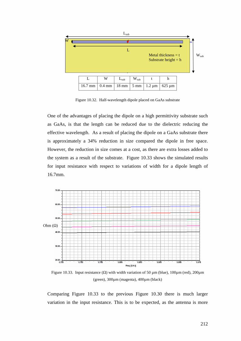
212
L W Lsub Wsub t h
16.7 mm 0.4 mm 18 mm 5 mm 1.2 µm 625 µm
Figure 10.32. Half-wavelength dipole placed on GaAs substrate
One of the advantages of placing the dipole on a high permittivity substrate such
as GaAs, is that the length can be reduced due to the dielectric reducing the
effective wavelength. As a result of placing the dipole on a GaAs substrate there
is approximately a 34% reduction in size compared the dipole in free space.
However, the reduction in size comes at a cost, as there are extra losses added to
the system as a result of the substrate. Figure 10.33 shows the simulated results
for input resistance with respect to variations of width for a dipole length of
16.7mm.
Figure 10.33. Input resistance (Ω) with width variation of 50 µm (blue), 100µm (red), 200µm
(green), 300µm (magenta), 400µm (black)
Comparing Figure 10.33 to the previous Figure 10.30 there is much larger
variation in the input resistance. This is to be expected, as the antenna is more
L
Ohm (Ω)
W
Metal thickness = t Substrate height = h
Wsub
Lsub
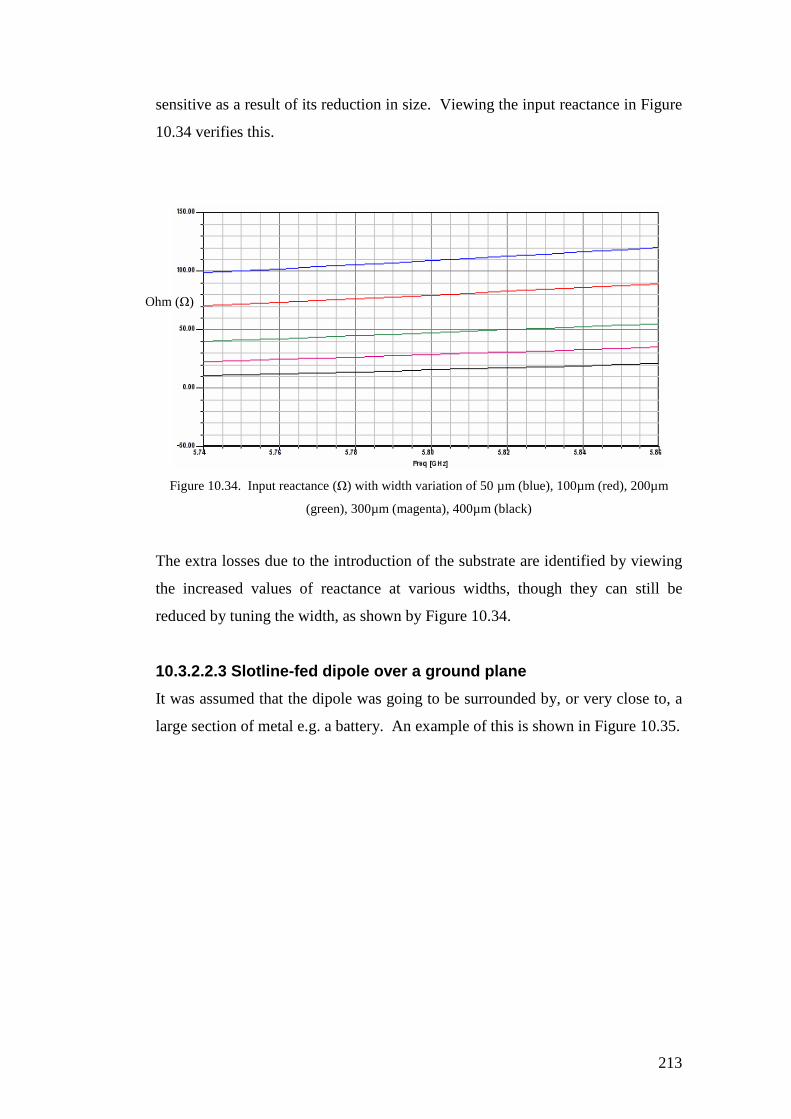
213
sensitive as a result of its reduction in size. Viewing the input reactance in Figure
10.34 verifies this.
Figure 10.34. Input reactance (Ω) with width variation of 50 µm (blue), 100µm (red), 200µm
(green), 300µm (magenta), 400µm (black)
The extra losses due to the introduction of the substrate are identified by viewing
the increased values of reactance at various widths, though they can still be
reduced by tuning the width, as shown by Figure 10.34.
10.3.2.2.3 Slotline-fed dipole over a ground plane
It was assumed that the dipole was going to be surrounded by, or very close to, a
large section of metal e.g. a battery. An example of this is shown in Figure 10.35.
Ohm (Ω)
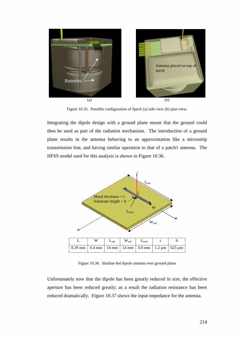
214
(a) (b)
Figure 10.35. Possible configuration of Speck (a) side view (b) plan view.
Integrating the dipole design with a ground plane meant that the ground could
then be used as part of the radiation mechanism. The introduction of a ground
plane results in the antenna behaving to an approximation like a microstrip
transmission line, and having similar operation to that of a patch1 antenna. The
HFSS model used for this analysis is shown in Figure 10.36.
L W Lsub Wsub Lfeed t h
8.39 mm 0.4 mm 14 mm 14 mm 0.8 mm 1.2 µm 625 µm
Figure 10.36. Slotline-fed dipole antenna over ground plane
Unfortunately now that the dipole has been greatly reduced in size, the effective
aperture has been reduced greatly; as a result the radiation resistance has been
reduced dramatically. Figure 10.37 shows the input impedance for the antenna.
Antenna placed on top of speck
Batteries
Lsub
Wsub
L
W Lfeed
Metal thickness = t Substrate height = h

215
Figure 10.37. Results for real (red) and imaginary (blue) input impedance for a printed dipole
antenna over a ground plane
The first resonance occurs at approximately 5.5 GHz with a very low value of
input resistance of 2.4Ω. This value of resistance is indicative of a very low value
of radiation resistance, which unsurprisingly will affect the antennas efficiency.
Evidence of this is shown in Figure 10.41 (b). This also corresponds with the
theory discussed in Section 10.3.1 that a reduction in size gives a reduction in
efficiency.
10.3.2.2.4 Folded dipole over a ground plane with transceiver
To try and reduce the area further, the arms of the antenna were folded around the
transceiver. It has already been reported by Nakano [21] that this has a minimal
effect on current and the far-field pattern for a 90 degree bend on a dipole. The
layout for a slotline-fed folded dipole with the transceiver body is shown in
Figure 10.38.
Ohm (Ω)
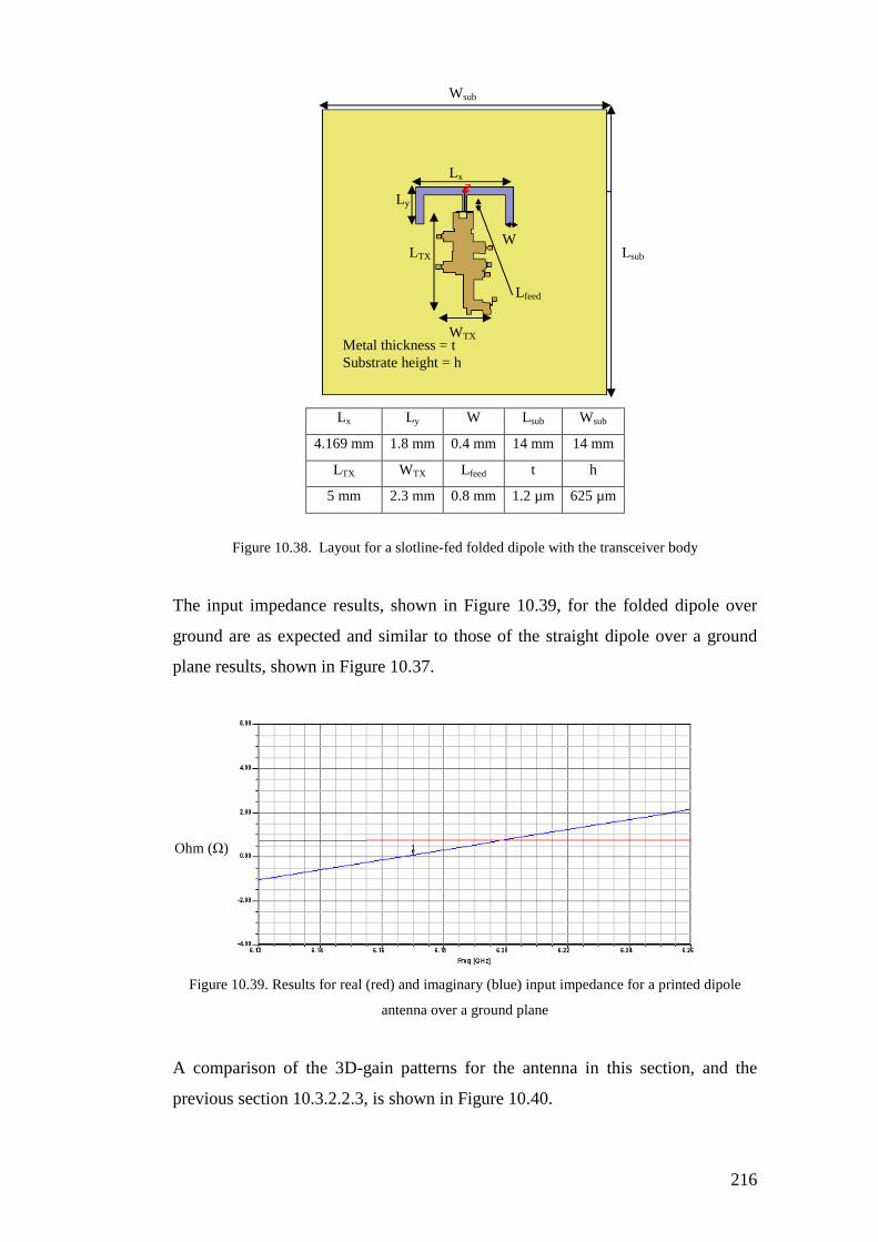
216
Lx Ly W Lsub Wsub
4.169 mm 1.8 mm 0.4 mm 14 mm 14 mm
LTX WTX Lfeed t h
5 mm 2.3 mm 0.8 mm 1.2 µm 625 µm
Figure 10.38. Layout for a slotline-fed folded dipole with the transceiver body
The input impedance results, shown in Figure 10.39, for the folded dipole over
ground are as expected and similar to those of the straight dipole over a ground
plane results, shown in Figure 10.37.
Figure 10.39. Results for real (red) and imaginary (blue) input impedance for a printed dipole
antenna over a ground plane
A comparison of the 3D-gain patterns for the antenna in this section, and the
previous section 10.3.2.2.3, is shown in Figure 10.40.
Lsub
Ly
Ohm (Ω)
Metal thickness = t Substrate height = h
Lx
W
Wsub
WTX
LTX
Lfeed
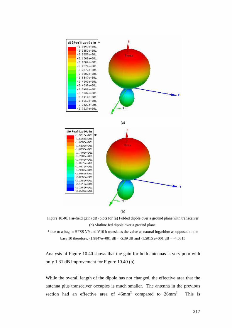
217
(a)
(b)
Figure 10.40. Far-field gain (dB) plots for (a) Folded dipole over a ground plane with transceiver
(b) Slotline fed dipole over a ground plane.
* due to a bug in HFSS V9 and V10 it translates the value as natural logarithm as opposed to the
base 10 therefore, -1.9847e+001 dB= -5.39 dB and -1.5015 e+001 dB = -4.0815
Analysis of Figure 10.40 shows that the gain for both antennas is very poor with
only 1.31 dB improvement for Figure 10.40 (b).
While the overall length of the dipole has not changed, the effective area that the
antenna plus transceiver occupies is much smaller. The antenna in the previous
section had an effective area of 46mm2 compared to 26mm2. This is
*
*
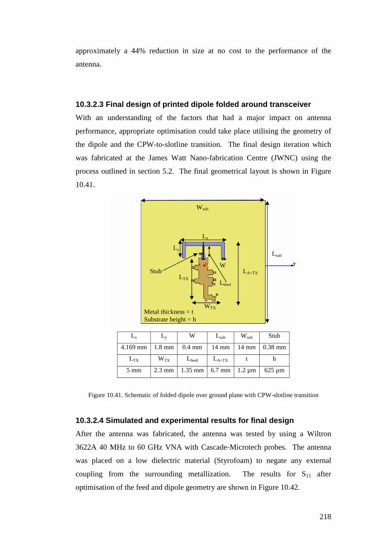
218
approximately a 44% reduction in size at no cost to the performance of the
antenna.
10.3.2.3 Final design of printed dipole folded around transceiver
With an understanding of the factors that had a major impact on antenna
performance, appropriate optimisation could take place utilising the geometry of
the dipole and the CPW-to-slotline transition. The final design iteration which
was fabricated at the James Watt Nano-fabrication Centre (JWNC) using the
process outlined in section 5.2. The final geometrical layout is shown in Figure
10.41.
Lx Ly W Lsub Wsub Stub
4.169 mm 1.8 mm 0.4 mm 14 mm 14 mm 0.38 mm
LTX WTX Lfeed LA+TX t h
5 mm 2.3 mm 1.35 mm 6.7 mm 1.2 µm 625 µm
Figure 10.41. Schematic of folded dipole over ground plane with CPW-slotline transition
10.3.2.4 Simulated and experimental results for final design
After the antenna was fabricated, the antenna was tested by using a Wiltron
3622A 40 MHz to 60 GHz VNA with Cascade-Microtech probes. The antenna
was placed on a low dielectric material (Styrofoam) to negate any external
coupling from the surrounding metallization. The results for S11 after
optimisation of the feed and dipole geometry are shown in Figure 10.42.
Stub W
Ly
Lx
Wsub
Lsub
Metal thickness = t Substrate height = h
Lfeed
WTX
LTX
LA+TX

219
Figure 10.42. Simulated (blue) and experimental (red) results for S11
Analysis of the results in Figure 10.42 shows a discrepancy between the simulated
and experimental resonant frequencies. One factor that can be discounted is
errors in the size of the antenna and transceiver metallization as it was
manufactured in the JWNC, which has a high fabrication precision. A possible
cause of error is that the substrate height may be smaller than indicated. Also, to
speed up the fabrication process, gold-wire bonds were used instead of standard
air-bridges. Another possible explanation for the discrepancy of simulated and
practical results is the proximity of the probe pad to the antenna. An interesting
point to note about the experimental results is that bandwidth is larger, so lower
Q, when compared to the simulated results. This can be attributed to extra
external losses occurring, most likely a result of the probe being in close
proximity to the antenna.
Analysis of the input impedance, shown in Figure 10.43, shows similar responses
for both experimental and simulated results, even though the operating frequency
is different.
S11 (dB)
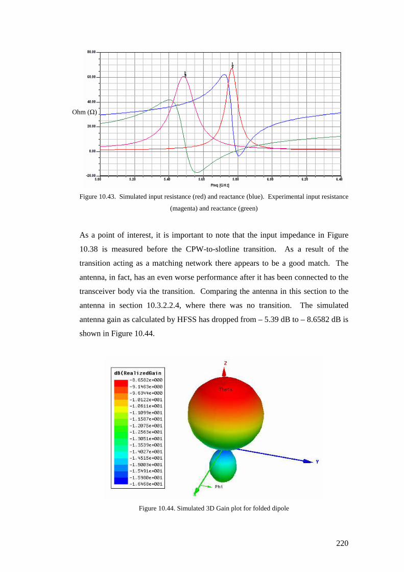
220
Figure 10.43. Simulated input resistance (red) and reactance (blue). Experimental input resistance
(magenta) and reactance (green)
As a point of interest, it is important to note that the input impedance in Figure
10.38 is measured before the CPW-to-slotline transition. As a result of the
transition acting as a matching network there appears to be a good match. The
antenna, in fact, has an even worse performance after it has been connected to the
transceiver body via the transition. Comparing the antenna in this section to the
antenna in section 10.3.2.2.4, where there was no transition. The simulated
antenna gain as calculated by HFSS has dropped from – 5.39 dB to – 8.6582 dB is
shown in Figure 10.44.
Figure 10.44. Simulated 3D Gain plot for folded dipole
Ohm (Ω)
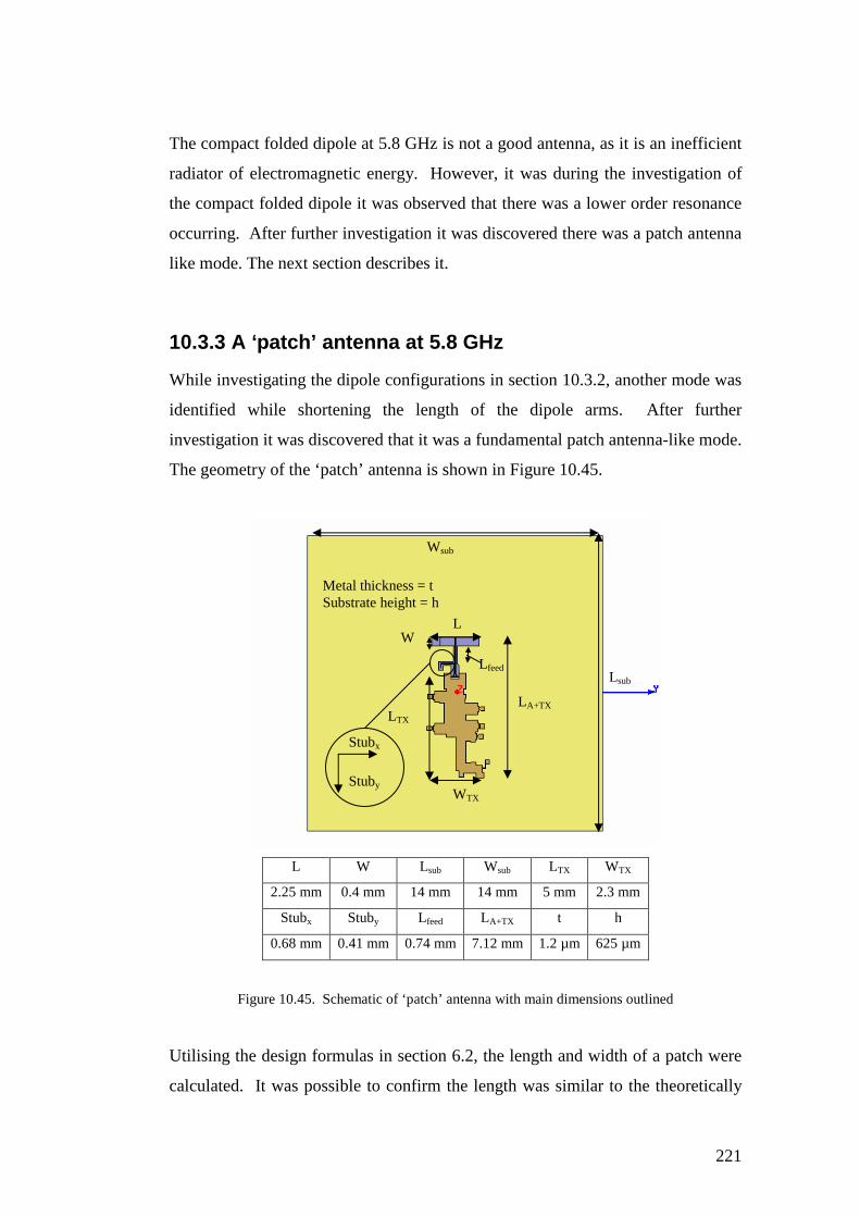
221
The compact folded dipole at 5.8 GHz is not a good antenna, as it is an inefficient
radiator of electromagnetic energy. However, it was during the investigation of
the compact folded dipole it was observed that there was a lower order resonance
occurring. After further investigation it was discovered there was a patch antenna
like mode. The next section describes it.
10.3.3 A ‘patch’ antenna at 5.8 GHz
While investigating the dipole configurations in section 10.3.2, another mode was
identified while shortening the length of the dipole arms. After further
investigation it was discovered that it was a fundamental patch antenna-like mode.
The geometry of the ‘patch’ antenna is shown in Figure 10.45.
L W Lsub Wsub LTX WTX
2.25 mm 0.4 mm 14 mm 14 mm 5 mm 2.3 mm
Stubx Stuby Lfeed LA+TX t h
0.68 mm 0.41 mm 0.74 mm 7.12 mm 1.2 µm 625 µm
Figure 10.45. Schematic of ‘patch’ antenna with main dimensions outlined
Utilising the design formulas in section 6.2, the length and width of a patch were
calculated. It was possible to confirm the length was similar to the theoretically
LA+TX
L
Lsub
Wsub
W
Stubx
Stuby
LTX
WTX
Lfeed
Metal thickness = t Substrate height = h
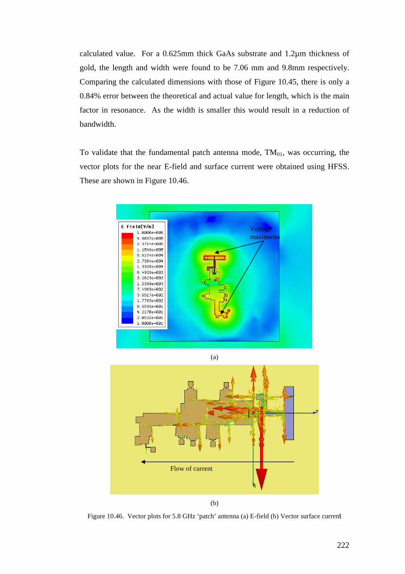
222
calculated value. For a 0.625mm thick GaAs substrate and 1.2µm thickness of
gold, the length and width were found to be 7.06 mm and 9.8mm respectively.
Comparing the calculated dimensions with those of Figure 10.45, there is only a
0.84% error between the theoretical and actual value for length, which is the main
factor in resonance. As the width is smaller this would result in a reduction of
bandwidth.
To validate that the fundamental patch antenna mode, TM01, was occurring, the
vector plots for the near E-field and surface current were obtained using HFSS.
These are shown in Figure 10.46.
(a)
(b)
Figure 10.46. Vector plots for 5.8 GHz ‘patch’ antenna (a) E-field (b) Vector surface current
Voltage maximums
Flow of current

223
Inspection of Figure 10.46 confirms the type of radiation associated with a patch
antenna. Figure 10.46 (a) shows two voltage maximums at the top and bottom of
the patch. Unfortunately, due to difficulty in mesh size, it was impossible to
obtain a sensible vector current plot for the electric field over the ‘patch’. There
is, however, verification that the two maximums are 180° out of phase, as Figure
10.46 (b) shows the surface current flowing in a uniform direction along the
length of the antenna, with a current maximum in the middle.
Figure 10.47. Simulated (blue) and experimental (green) S11 results for ‘patch’ antenna
Experimental results were obtained for the ‘patch’ antenna using the process
described in section 10.3.2.2.6 and are shown in Figure 10.47 along with the
simulated results. Inspection of the results in Figure 10.47 shows relatively good
agreement between the simulated and experimental results, especially when
compared to the compact-folded dipole results. There is a slight mismatch in the
operating frequency with the ‘patch’ antenna, which resonates at 5.92 GHz
instead of 5.8 GHz. As with the folded dipole discussed in the previous section,
there appears to be a wider operational bandwidth for the experimental result,
when compared to the simulated response. This can possibly be attributed to
extra losses added caused by the close proximity of the probe over the antenna.
Mag S11 (dB)
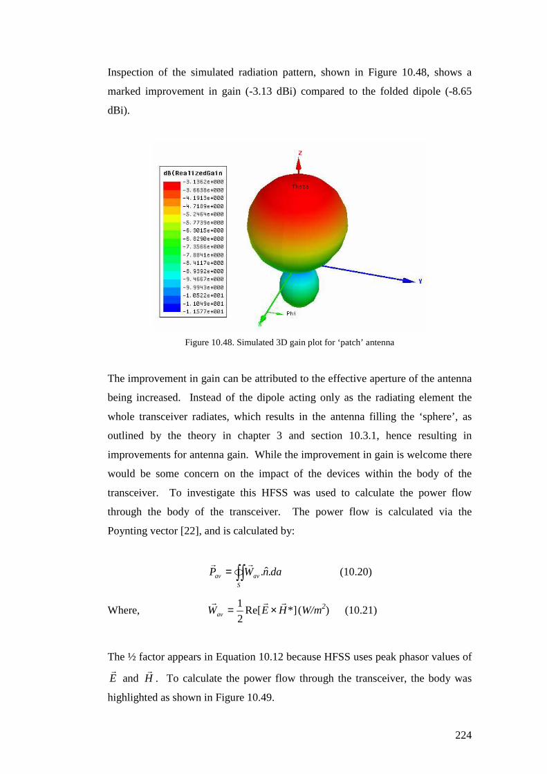
224
Inspection of the simulated radiation pattern, shown in Figure 10.48, shows a
marked improvement in gain (-3.13 dBi) compared to the folded dipole (-8.65
dBi).
Figure 10.48. Simulated 3D gain plot for ‘patch’ antenna
The improvement in gain can be attributed to the effective aperture of the antenna
being increased. Instead of the dipole acting only as the radiating element the
whole transceiver radiates, which results in the antenna filling the ‘sphere’, as
outlined by the theory in chapter 3 and section 10.3.1, hence resulting in
improvements for antenna gain. While the improvement in gain is welcome there
would be some concern on the impact of the devices within the body of the
transceiver. To investigate this HFSS was used to calculate the power flow
through the body of the transceiver. The power flow is calculated via the
Poynting vector [22], and is calculated by:
∫∫=S
avav danWP .ˆ.rr
(10.20)
Where, *]Re[2
1HEWav
rrr×= (W/m2) (10.21)
The ½ factor appears in Equation 10.12 because HFSS uses peak phasor values of
Er
and Hr
. To calculate the power flow through the transceiver, the body was
highlighted as shown in Figure 10.49.

225
Figure 10.49. Transceiver body highlighted for Poynting vector calculation
Using the field calculator facility in HFSS it is possible to select an arbitrary
surface and calculate the power flow through it as follows.
As is standard with HFSS the input power (Pin) to the antenna port is 1 Watt. To
convert to dBm the following formula is used:
dBmmW
WLog
mW
PLogdBmP in
in 301
110
110)( 1010 =
=
= (10.22)
From HFSS, the value of power flow (avPr
) through the transceiver is 0.117 Watts
which equates to:
dBmmW
LogdBmPav 7.201
117.010)( 10 =
= (10.23)
This means that amount of power flowing through the transceiver is 9.3 dB less
than the input power. Using this data it is possible to speculate how much power
would flow through the transceiver discussed in section 10.1. For the transceiver
in section 10.1 the output power was equal to -10.85 dBm, which means -10.85
dBm inputted at the terminals of the antenna. To calculate the power flow
through the transceiver the process of 10.13 and 10.14 is reversed, as follows:
dBmdBmdBmdBmPav 55.207.985.10)( −=−−= (10.24)
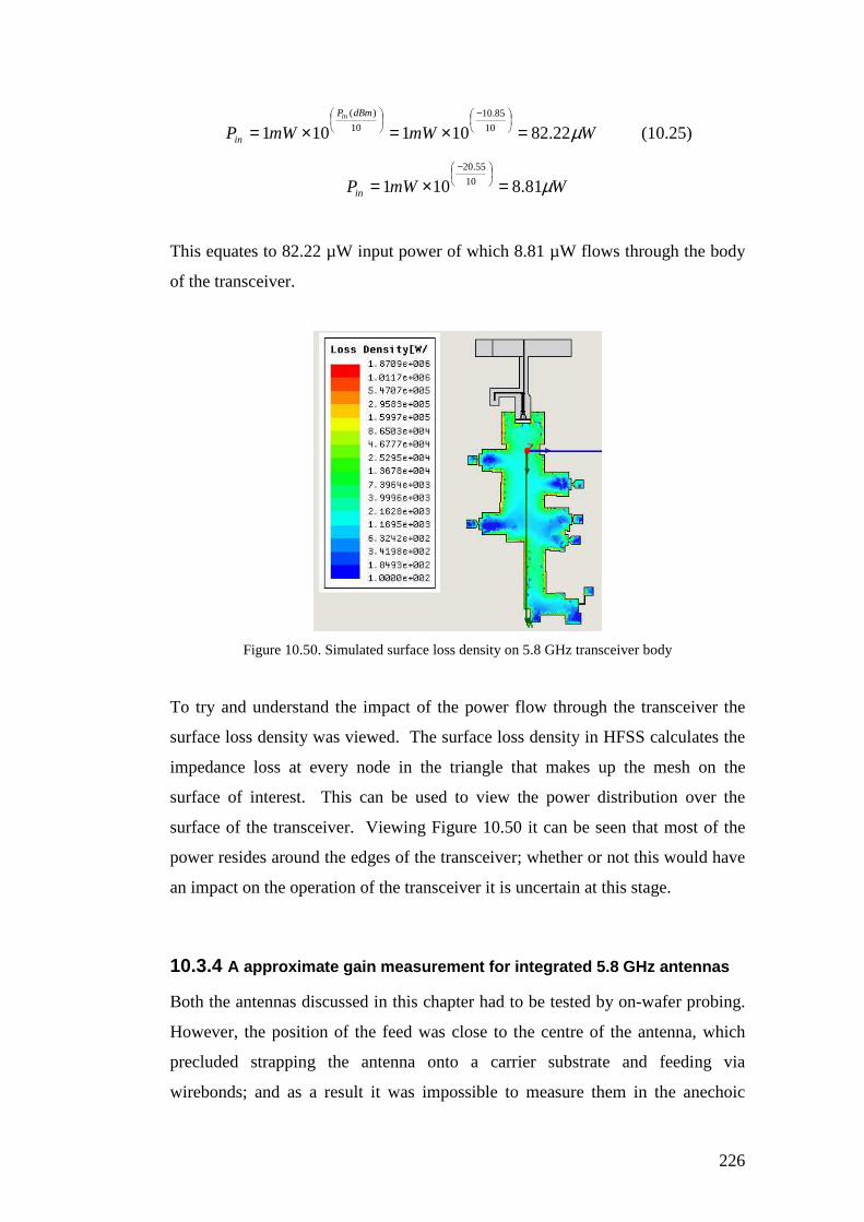
226
WmWmWPdBmP
in
in
µ22.82101101 10
85.10
10
)(
=×=×=
−
(10.25)
WmWPin µ81.8101 10
55.20
=×=
−
This equates to 82.22 µW input power of which 8.81 µW flows through the body
of the transceiver.
Figure 10.50. Simulated surface loss density on 5.8 GHz transceiver body
To try and understand the impact of the power flow through the transceiver the
surface loss density was viewed. The surface loss density in HFSS calculates the
impedance loss at every node in the triangle that makes up the mesh on the
surface of interest. This can be used to view the power distribution over the
surface of the transceiver. Viewing Figure 10.50 it can be seen that most of the
power resides around the edges of the transceiver; whether or not this would have
an impact on the operation of the transceiver it is uncertain at this stage.
10.3.4 A approximate gain measurement for integrated 5.8 G Hz antennas
Both the antennas discussed in this chapter had to be tested by on-wafer probing.
However, the position of the feed was close to the centre of the antenna, which
precluded strapping the antenna onto a carrier substrate and feeding via
wirebonds; and as a result it was impossible to measure them in the anechoic
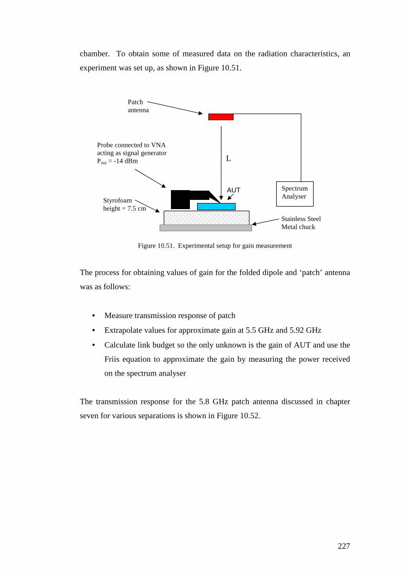
227
chamber. To obtain some of measured data on the radiation characteristics, an
experiment was set up, as shown in Figure 10.51.
Figure 10.51. Experimental setup for gain measurement
The process for obtaining values of gain for the folded dipole and ‘patch’ antenna
was as follows:
• Measure transmission response of patch
• Extrapolate values for approximate gain at 5.5 GHz and 5.92 GHz
• Calculate link budget so the only unknown is the gain of AUT and use the
Friis equation to approximate the gain by measuring the power received
on the spectrum analyser
The transmission response for the 5.8 GHz patch antenna discussed in chapter
seven for various separations is shown in Figure 10.52.
AUT
L
Spectrum Analyser
Patch antenna
Styrofoam height = 7.5 cm
Probe connected to VNA acting as signal generator Pout = -14 dBm
Stainless Steel Metal chuck
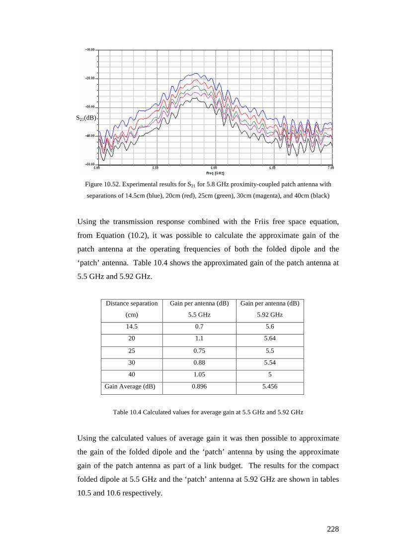
228
Figure 10.52. Experimental results for S21 for 5.8 GHz proximity-coupled patch antenna with
separations of 14.5cm (blue), 20cm (red), 25cm (green), 30cm (magenta), and 40cm (black)
Using the transmission response combined with the Friis free space equation,
from Equation (10.2), it was possible to calculate the approximate gain of the
patch antenna at the operating frequencies of both the folded dipole and the
‘patch’ antenna. Table 10.4 shows the approximated gain of the patch antenna at
5.5 GHz and 5.92 GHz.
Distance separation
(cm)
Gain per antenna (dB)
5.5 GHz
Gain per antenna (dB)
5.92 GHz
14.5 0.7 5.6
20 1.1 5.64
25 0.75 5.5
30 0.88 5.54
40 1.05 5
Gain Average (dB) 0.896 5.456
Table 10.4 Calculated values for average gain at 5.5 GHz and 5.92 GHz
Using the calculated values of average gain it was then possible to approximate
the gain of the folded dipole and the ‘patch’ antenna by using the approximate
gain of the patch antenna as part of a link budget. The results for the compact
folded dipole at 5.5 GHz and the ‘patch’ antenna at 5.92 GHz are shown in tables
10.5 and 10.6 respectively.
S21(dB)

229
Distance
Separation (cm)
Signal Received
(dBm)
Calculated Gain
(dB)
10 -54 -14
15 -57 -13.2
20 -59 -12.7
25 -61 -12.7
30 -63 -13.1
35 -61 -9.7
Table 10.5. Folded dipole - Signal received on spectrum analyser via patch antenna for various
separations with the calculated value of gain
Distance
Separation (cm)
Signal Received
(dBm)
Calculated Gain
(dB)
10 -49 -12.6
15 -52 -12.1
20 -52 -9.6
25 -52 -7.7
30 -50 -4.1
35 -52 -4.7
Table 10.6. ‘Patch’ antenna - Signal received on spectrum analyser via patch antenna for various
separations with the calculated value of gain
Inspection of the results in table 10.5 and 10.6 show some confirmation of the
simulated results. Both antennas gains are a lower than the simulated response
but it is clear that the patch antenna has an overall better response. One
interesting phenomenon, occurring with both sets of results, is the improvement
on the signal level being received the further the antenna is moved from the AUT.
The minimum separation of 10 cm (patch maximum diameter = 50 mm) was used
to ensure that the patch was in the far-field, so it is unlikely that the phenomena
occurs by the antenna being in the near-field. However, there is the possibility
that the probe arm used to test the antenna increased the maximum linear
dimension of the antenna and as a result the far-field boundary was greater than
10 cm. Another possible explanation is that there is some form of multi-path

230
constructive/destructive interference as well as absorption occurring because of
the presence of the metal chuck in the measurement system. The presence of the
probe can explain the lower than expected values of signal received as the
maximum attenuation occurring in the cables was about 1dB.
Both the antennas investigated in this chapter have given a useful insight into the
problems of miniaturisation. However, the folded dipole can probably be
discarded as a possible integrated antenna for the transceiver due to its very poor
performance. The ‘patch’ antenna, however, offers a lot of promise. Gain
improvements can be obtained by optimising the shape of the transceiver. It may
also be possible to excite a circularly-polarised wave, increasing the suitability of
the antenna for wireless sensor networks.
231
11. Discussion and conclusions
The work in this thesis presents a wide ranging insight into the design, fabrication
and testing of antennas that are suitable for wireless sensor networks, and in
particular, those required by the Speckled Computing Consortium.
To give an understanding into the research carried out in this project, the essence
of what an antenna is, and how it radiates, was outlined. An in-depth study of the
dipole provided the fundamental basis of the majority of work carried out in this
project. As some of the antennas were defined as electrically small a review of
fundamental limitations of antennas was carried out. An antenna does not radiate
by itself, so an appreciation had to be gained of the feeding methods; in the case
of this project feeds were provided by planar transmission lines such as
microstrip, CPW and slotline. Also reviewed were the fundamental parameters
used to characterise antennas in this thesis, including impedance bandwidth, S-
parameters, radiation pattern, directivity, antenna efficiency, gain and
polarisation.
Antennas were designed, manufactured and tested using conventional printed
circuit boards (PCB’s), and Gallium Arsenide (GaAs) substrates, operating at a
range of frequencies from 2.4 GHz to 12 GHz. Available at Glasgow University
was a wide range of test equipment and software for an antenna design engineer.
The 3D electromagnetic simulation software, HFSS, was used for every antenna
designed in this thesis. This software was combined with a powerful PC to
increase the design accuracy through finer meshing. Various VNA and spectrum
analysers were used to obtain many of the fundamental parameters used to
characterise antennas. The anechoic chamber installed at the end of the project
allowed for radiation pattern characterisation of the patch and UWB antennas,
discussed in chapters six and eight, respectively.
A large part of this research was conducted in the area of UWB antenna design,
simulation and testing. Using the fundamental antenna parameters outlined at the
start of the thesis, chapters seven and eight highlighted the extra complexity
required for UWB antenna design, such as increased impedance band width from
232
3.1 – 10.16 GHz, group delay and phase. The initial UWB antennas investigated
in chapter 8 were used to give an appreciation of the two of the main types of
antenna that could be designed for UWB. The Vivaldi antenna, which had a wide
bandwidth, was directional and had an excellent pulse response but was
electrically very large. Also due to its size it was operating in the reactive near-
field and was deemed unsuitable for short-range wireless sensor networks. The
CPW-fed monopole was the opposite, as it was compact, omni-directional but had
a poor pulse response and impedance bandwidth response compared to the
Vivaldi.
As the collaborative channel-modelling project between Strathclyde and Glasgow
Universities required an omni-directional antenna, the UWB dipole was proposed
as a possible candidate. The main drawback was the need to provide a balanced
feed that did not excite leakage current. Four antennas were investigated, a
microstrip-fed UWB dipole, a CPW-fed UWB dipole, a hybrid-feed UWB dipole,
and a tapered-feed UWB dipole and these were fully characterised using the
fundamental antenna parameters and radiation patterns obtained at 3, 6, and 9
GHz. All four antennas satisfied the impedance bandwidth criteria, but there was
differing performance in terms of radiation pattern and pulse transmission. The
antenna with the best radiation pattern was the CPW-fed UWB dipole with slots,
while the tapered feed UWB dipole gave the best performance for pulse
transmission.
An anechoic chamber was installed at Glasgow University in 2007, in the latter
part of this thesis work. The results for the radiation patterns presented in
chapters six and eight were obtained from the near-field data, whilst not ideal the
data still provided useful insight. The software supplied by Near-field Systems Inc
(NSI) takes the near-field data, which was used in this thesis and applies a Fourier
transform to change it to the far-field. The data obtained from far-field transform
was at best very noisy, and quite often illogical. Whether this can be attributed to
a system error, or human error, is unknown at this stage and further investigation
is required.
233
The hybrid- and tapered-feed UWB dipole radiation pattern responses were
disappointing. Further research is required to identify the discrepancy between
the simulated and experimental results. A possible and quite likely reason was the
manufacturing methods employed, as both antennas were assembled by hand and
misalignment was likely. As the hybrid-feed UWB dipole was constructed with
multiple substrates, the alignment between the feed and the elements was hard to
engineer; further development should be conducted into improving the procedure.
For the tapered-feed UWB dipole a more elegant way of inserting the feed needs
to be devised.
Chapter 10 focused on the antenna design work directly related to the Speckled
Computing Consortium objective of designing a 5mm3 ‘Speck’. Discussed in this
Chapter 10 was the radio architectures used, such as the diode rectifier method
and the super-regenerative receiver, which had low power consumptions that will
meet the overall power consumption target of less than 400 µW.
This thesis investigated several antennas that were narrowband and electrically
small. The 2.45 GHz Rectaxial antenna had excellent matching (S11 = -20dB) at
the frequency of operation and an omni-directional radiation pattern with a
maximum gain of 2.69 dBi, as measured in a far-field anechoic chamber. An
attempt was made to reduce the size of the antenna by increasing the frequency of
operation to 5.8 GHz. Unfortunately, due to excitation of surface waves along the
ground plane this distorted the radiation pattern and, due to the unpredictability of
results, the Rectaxial antenna was deemed unsuitable for operation at 5.8 GHz or
greater.
After identifying the limitations of the rectaxial antenna at 5.8 GHz, other
antennas were investigated. These were the compact-folded dipole and the
‘patch’ antenna, which were fabricated on GaAs and designed to be integrated
around a MMIC transceiver to operating at 5.8 GHz. The compact-folded dipole
was found to be an extremely poor radiator of electromagnetic energy, with an
experimentally obtained value of gain = -14 dB. This poor gain, coupled with the
unpredictability in its resonant frequency (simulated = 5.8 GHz; experimental =
5.5 GHz), made it a poor choice for a integrated antenna. However, the ‘patch’

234
antenna was very promising, with acceptable gain (- 4 to -7 dB) and reasonable
correlation between simulated (5.8 GHz) and experimental (5.92 GHz) resonant
frequency.
Further research needs to be conducted into improving the gain, and potential
impact of crosstalk on the active circuitry due to the entire transceiver radiating.
Also, an accurate method of obtaining a radiation pattern for the ‘patch’ antenna
needs to be identified. This would also include an alternative way of feeding the
‘patch’ antenna so that wafer probes would not interfere with the ‘patch’.

235
12. List of References
12.1 Chapter 1
[1] www.specknet.org
[2] http://robotics.eecs.berkeley.edu/~pister/SmartDust/
12.2 Chapter 2
[1] J. C. Maxwell “A treatise on electricity and magnetism” Vol 1 & 2, Mitchell
Library copy, Glasgow
[2] Constantine A. Balanis: “Antenna theory, analysis and design” Third edition,
John Wiley & Sons, Inc. ISBN 0-471-60639-1. Chapter 1, pg 1.
ISBN 0-07-112240-0, Chapter 6, pp 170
[3] Constantine A. Balanis: “Antenna theory, analysis and design”. Third edition,
John Wiley & Sons, Inc. ISBN 0-471-60639-1. Chapter 1, pp 2.
[4] Constantine A. Balanis: “Antenna theory, analysis and design” Third edition,
John Wiley & Sons, Inc. ISBN 0-471-60639-1. Chapter 1, pp 9.
[5] Constantine A. Balanis: “Antenna theory, analysis and design” Third edition,
John Wiley & Sons, Inc. ISBN 0-471-60639-1. Chapter 1, pp 10.
[6] J. D. Krauss, “Antennas For All Applications”, Third edition, McGraw-Hill,
ISBN 0-07-112240-0, Chapter 2, pp 38
[7] Constantine A. Balanis: “Antenna theory, analysis and design” Third edition,
John Wiley & Sons, Inc. ISBN 0-471-60639-1. Chapter 1, pp 13.
[8] J. D. Krauss, “Antennas For All Applications”, Third edition, McGraw-Hill,
[9] David M. Pozar, “Microwave Engineering”, 2nd Edition, John Wiley & Sons,
Inc, ISBN 0-471-17096-8, Chapter 1 pp 16-17
[10] Constantine A. Balanis: “Antenna theory, analysis and design” Third edition,
John Wiley & Sons, Inc. ISBN 0-471-60639-1. Chapter 4, pg 152.
[11] Constantine A. Balanis: “Antenna theory, analysis and design” Third edition,
John Wiley & Sons, Inc. ISBN 0-471-60639-1. Chapter 4, pg 152.
[12] J. D. Krauss, “Antennas For All Applications”, Third edition, McGraw-Hill,
ISBN 0-07-112240-0, Chapter 6, pg 167
[13] J. D. Krauss, “Antennas For All Applications”, Third edition, McGraw-Hill,
ISBN 0-07-112240-0, Chapter 6, pg 168

236
[14] J. D. Krauss, “Antennas For All Applications”, Third edition, McGraw-Hill,
ISBN 0-07-112240-0, Chapter 6, pp 177
[15] J. D. Krauss, “Antennas For All Applications”, Third edition, McGraw-Hill,
ISBN 0-07-112240-0, Chapter 6, pp 177
12.3 Chapter 3
[1] H. A. Wheeler, “Fundamental Limitations of Small Antennas,” Proceedings of
the IRE, vol. 35, pp. 1479-1484, Dec. 1947
[2] H. A. Wheeler, “Small Antennas”, IEEE Antennas & Propagation, AP-23, 4,
pp 462-469, 1975
[3] L. J. Chu, “Physical limitations on omni-directional antennas,” J. Appl. Phys.,
vol. 19, pp. 1163-1175, Dec. 1948.
[4] Constantine A. Balanis: “Antenna theory, analysis and design” Third edition,
John Wiley & Sons, Inc. ISBN 0-471-60639-1. Chapter 11, pp 638
[5] R.C. Hansen, “Fundamental Limitations in Antennas,” IEEE, vol. 69, pgs 170-
182, February 1981
[6] J. S. McLean, “A re-examination of the fundamental limits on the radiation Q
of electrically small antennas,” IEEE Transaction on Antennas and Propagation,
vol. 44, pp. 672-675, May 1996.
[7] Hans Schantz, “The Art and Science of Ultra Wideband Antennas”, Artech
House, ISBN 1-58053-888-6, Chapter 5, pp 179
[8] Skrivervik, A.K.; Zurcher, J.-F.; Staub, O.; Mosig, J.R.; “PCS antenna design:
the challenge of miniaturization” Antennas and Propagation Magazine, IEEE
Volume 43, Issue 4, Aug. 2001 Page(s):12 - 27
12.4 Chapter 4
[1] David M. Pozar, “Microwave Engineering”, 2nd Edition, John Wiley & Sons,
Inc, ISBN 0-471-17096-8, Chapter 2 pp 58-59
[2] David M. Pozar, “Microwave Engineering”, 2nd Edition, John Wiley & Sons,
Inc, ISBN 0-471-17096-8, Chapter 2 pp 62
[3] David M. Pozar, “Microwave Engineering”, 2nd Edition, John Wiley & Sons,
Inc, ISBN 0-471-17096-8, Chapter 2 pg 119

237
[4] David M. Pozar, “Microwave Engineering”, 2nd Edition, John Wiley & Sons,
Inc, ISBN 0-471-17096-8, Chapter 2 pg 65
[5] K.C. Gupta, R. Garg, and I. J. Bahl, “Microstrip Lines and Slotlines”, Artech
House, 1979
[6] David M. Pozar, “Microwave Engineering”, 2nd Edition, John Wiley & Sons,
Inc, ISBN 0-471-17096-8, Chapter 3 pg 162
[7] K.C. Gupta, R. Garg, and I. J. Bahl, “Microstrip Lines and Slotlines”, Artech
House, 1979
[8] S. B. Cohn, “Slotline on a dielectric substrate,” IEEE Trans. Microwaue
Theory and Tech., vol. MTT-17, pp. 768-778, Oct. 1969.
[9] K.C. Gupta, R. Garg, and I. J. Bahl, “Microstrip Lines and Slotlines”, Artech
House, 1979
[10] K.C. Gupta, R. Garg, and I. J. Bahl, “Microstrip Lines and Slotlines”, Artech
House, 1979
12.5 Chapter 5
[1] David M. Pozar, “Microwave Engineering”, 2nd Edition, John Wiley & Sons,
Inc, ISBN 0-471-17096-8, Chapter 3 pp 66-68
[2] IEEE “IEEE Standard Definitions of Terms for Antennas” Published by The
Institute of Electrical and Electronics Engineers, Inc 345 East 47th Street, New
York, NY 10017, USA, June 22, 1983, pg 24
[3] Constantine A. Balanis: “Antenna theory, analysis and design” Third edition,
John Wiley & Sons, Inc. ISBN 0-471-60639-1. Chapter 2, pg 28.
[4] IEEE “IEEE Standard Definitions of Terms for Antennas” Published by The
Institute of Electrical and Electronics Engineers, Inc 345 East 47th Street, New
York, NY 10017, USA, June 22, 1983, pg 12
[5] J. D. Krauss, “Antennas”, Chapter 7, 1st Edition, McGraw-Hill, 1950, Chapter
3, pp 42-43
[6] IEEE “IEEE Standard Definitions of Terms for Antennas” Published by The
Institute of Electrical and Electronics Engineers, Inc 345 East 47th Street, New
York, NY 10017, USA, June 22, 1983, pg 15
[7] IEEE “IEEE Standard Definitions of Terms for Antennas” Published by The
Institute of Electrical and Electronics Engineers, Inc 345 East 47th Street, New
York, NY 10017, USA, June 22, 1983, pg 23

238
[8] Constantine A. Balanis: “Antenna theory, analysis and design” Third edition,
John Wiley & Sons, Inc. ISBN 0-471-60639-1. Chapter 2, pp 70-75.
12.6 Chapter 6
[1] Park, Y.-J., Herschlein, A., Wiesbeck, W. “A Photonic Bandgap Structure for
Guiding and Suppressing Surface Waves in Millimeter Wave Antennas”, IEEE
Transactions On Microwave Theory and Techniques, Vol. 49, No. 10, October
2001 (Part 2 of 2), pp 1854-1859
[2] S. Wi, J. Kim, N. Kang, J. Kim, H. Yang, Y. Kim, J. Yook, “Package-Level
Integrated LTCC Antenna for RF Package Application”, IEEE Transactions on
Advanced Packaging, Vol. 30, NO. , February 2007, pp 132 – 141
[3] http://www.ansoft.com/products/hf/hfss/
[4] Girish Kumar, K.P. Ray, “Broadband Microstrip Antennas”, Artech House,
ISBN: 1-58053-244-6, Chapter 2, pg 7
[5] Dan Slater, “Near-Field Antenna Measurements”, Artech House, ISBN
Number: 0-89006-361-3, 1991, Chapter 2, pp 7-25
12.7 Chapter 7
[1] Constantine A. Balanis: “Antenna theory, analysis and design” Third edition,
John Wiley & Sons, Inc. ISBN 0-471-60639-1. Chapter 14, pg 28.
[2] Constantine A. Balanis: “Antenna theory, analysis and design” Third edition,
John Wiley & Sons, Inc. ISBN 0-471-60639-1. Chapter 14, pg 28.
[3] Constantine A. Balanis: “Antenna theory, analysis and design” Third edition,
John Wiley & Sons, Inc. ISBN 0-471-60639-1. Chapter 14, pg 28.
[4] James, J. R., and P.S. Hall, “Handbook of Microstrip Antennas”, Vol. 1,
London: Peter Peregrinus Ltd., 1989
[5] Girish Kumar, K.P. Ray, “Broadband Microstrip Antennas”, Artech House,
ISBN: 1-58053-244-6, Chapter 2, pp 36-37
[6] David M. Pozar, “Microwave Engineering”, 2nd Edition, John Wiley & Sons,
Inc, ISBN 0-471-17096-8, Chapter 2 pp 89-90
12.8 Chapter 8
[1] J.C. Adams et al, “Ultra-wideband for navigation and communications,” IEEE
Aerospace Conference Proceedings, Vol.2, 2001, pp. 785-792

239
[2] Ernest R. Kretzmer “Interference Characteristics of Pulse-Time Modulation”,
PROCEEDINGS OF THE I.R.E., March 1950, pp 252-255
[3] Jung N. Lee et al, “Design of a compact frequency-notched UWB slot
antenna”, Microwave and Optical Technology Letters Volume 48, Issue 1 , pp
105 – 107
[4] Seong H. Lee, Jong K. Park, Jung N. Lee, “ A novel CPW-fed ultra-wideband
antenna design”, Microwave and Optical Technology Letters Volume 44, Issue 5 ,
pp 393 - 396
[5] Stanislav Licul et al “A parametric study of time-domain characteristics of
possible UWB antenna architectures”, Vehicular Technology Conference, 2003.
VTC 2003-Fall. 2003, IEEE 58th, Volume: 5, pp 3110- 3114
[6] P.J. Gibson, “The Vivaldi Aerial”, 9th European Microwave Conference Proc.,
1979
[7] K. Chung et al, “Wideband CPW-fed monopole antenna with parasitic
elements and slots” Electronics Letters, Vol. 40, Issue 17, 19 Aug. 2004, pp1038-
1040.
[8] I. McGregor, G.Whyte, E.Wasige and I. Thayne, “UWB TEST SYSTEM”
Biennial Analog Signal Processing Conference, Oxford-Brookes College,
November 2004
[9] Mikhnev, V. Vainikainen, P., “Wideband Tapered-Slot Antenna With
Corrugated Edges For GPR Applications”, EUROPEAN MICROWAVE
CONFERENCE, 2003, VOL 33; VOL 2, pp 727-730
[10] Aiello, G.R., Rogerson, G.D., “Ultra-wideband wireless systems”,
Microwave Magazine, IEEE, June 2003, Volume: 4, Issue: 2
[11] Narayan Prasad Agrawall, Girish Kumar, and K. P. Ray, Wide-Band Planar
Monopole Antennas, IEEE TRANSACTIONS ON ANTENNAS AND
PROPAGATION, VOL. 46, NO. 2, FEBRUARY 1998, pp 294 -295
12.9 Chapter 9
[1] Hans Schantz, "Planar Elliptical Element Ultra-Wideband Dipole Antennas,"
Proceedings of the IEEE, APS Conference (2002).
[2] Do-Hoon Kwon, Yongjin Kim, “Suppression of Cable Leakage Current for
Edge-Fed Printed Dipole UWB Antennas Using Leakage-Blocking Slots”, IEEE

240
ANTENNAS AND WIRELESS PROPAGATION LETTERS, VOL. 5, 2006, pp
183-186
[3] Yoon, I.-J.; Hyungrak Kim; Kihun Chang; Young Joong Yoon; Young-Hwan
Kim; “Ultra wideband tapered slot antenna with band-stop characteristic”
Antennas and Propagation Society International Symposium, 2004. IEEE Volume
2, 20-25 June 2004 Page(s):1780 - 1783 Vol.2
[4] Hyungkuk Yoon; Hyungrak Kim; Kihun Chang; Young Joong Yoon; Young-
Hwan Kim; “A study on the UWB antenna with band-rejection characteristic”,
Antennas and Propagation Society International Symposium, 2004. IEEE Volume
2, 20-25 June 2004 pp1784 - 1787 Vol.2
[5] Schantz, H.G.; “ Bottom fed planar elliptical UWB antennas” Ultra Wideband
Systems and Technologies, 2003 IEEE Conference on 16-19 Nov. 2003 pp 219 -
223
[6] Duncan, J.W. and V.P. Minerva, “100:1 Bandwidth Balun Transformer”,
Proceedings of the IRE, Vol. 48, 1960, pp. 156-164
[7] www.matchcad.com
12.10 Chapter 10
[1] E. H. Armstrong, “Some recent developments of regenerative circuits”, Proc.
Inst . Radio Eng, Vol 10, pp. 244-260 Aug. 1922
[2] I.Mcgregor, I.; Whyte, G.; Elgaid, K.; Wasige, E.; Thayne, I.; “A 700µW
Tx/400µW Rx 2.4GHz Super - Regenerative GaAs Transceiver” Microwave
Conference, 2006. 36th European 10-15 Sept. 2006 pp1523 - 1525
[3] Constantine A. Balanis: “Antenna theory, analysis and design” Third edition,
John Wiley & Sons, Inc. ISBN 0-471-60639-1. Chapter 2, pp 94-96.
[4] J. D. Krauss, “Antennas”, Chapter 7, 1st Edition, McGraw-Hill, 1950, Chapter
7
[5] J. D. Krauss, “Antennas”, Chapter 7, 1st Edition, McGraw-Hill, 1950, Chapter
7, pg 175
[6] J. D. Krauss, “Antennas”, Chapter 7, 1st Edition, McGraw-Hill, 1950, Chapter
7, pg 180
[7] J. D. Krauss, “Antennas”, Chapter 7, 1st Edition, McGraw-Hill, 1950, Chapter
7, pg 157

241
[8] Whyte, G, "An Omnidirectiona, Low Cost, Low Profile, 2.45 GHz Microstrip
Fed Rectaxial Antenna for Wirelss Sensor Network Applications" IEE and IEEE
conference, Loughborough Antennas and Propagation Conference, LAPC 2006.
[9] J. D. Krauss, “Antennas”, Chapter 7, 1st Edition, McGraw-Hill, 1950. Chapter
7
[10] Chien-Jen Wang et al, “Small Microstrip Helical Antenna”. Microwave
Conference, 1999 Asia Pacific, Volume 2, 30 Nov.-3 Dec. 1999 pp 367 - 370.
[11] Jung-Ick Moon and Seong-Ook Park, “Small Chip Antenna for 2.4/5.8 GHz
Dual ISM-Band Applications”, IEEE Antennas and Wireless Propagation Letters
2003, Vol. 2, pp 313-315.
[12] www.ofcom.org.uk
[13] David M. Pozar, “Microwave Engineering”, 2nd Edition, John Wiley & Sons,
Inc, ISBN 0-471-17096-8, Chapter 3 pg 157
[14] David M. Pozar, “Microwave Engineering”, 2nd Edition, John Wiley & Sons,
Inc, ISBN 0-471-17096-8, Chapter 3 pg 151
[15] K. R. Karver and J. W. Mink, “Microstrip Antenna Technology”, IEEE
Trans. Antennas and Propagation., Vol. AP-29, No. 1, pp.25-27, January 1981
[16] Constantine A. Balanis: “Antenna theory, analysis and design” Third edition,
John Wiley & Sons, Inc. ISBN 0-471-60639-1. Chapter 14, pp 853 - 854.
[17] Khaled Elgaid Thesis, Dept. Of E & E Engineering, Glasgow University
[18] David M. Pozar, “Microwave Engineering”, 2nd Edition, John Wiley & Sons,
Inc, ISBN 0-471-17096-8, Chapter 2 pp 73-79
[19] J. D. Krauss, “Antennas”, Chapter 7, 1st Edition, McGraw-Hill, 1950,
Chapter 7, pg 245
[20] H. Nakano, J. Yamauchi, K. Kawashima, and K. Hirose, “Effects of arm
bend andasymmetric feeding on dipole antennae,’’ Int. J. Electron., vol.
55, pp. 353-364, 1983
[21] Constantine A. Balanis: “Antenna theory, analysis and design” Third edition,
John Wiley & Sons, Inc. ISBN 0-471-60639-1. Chapter 2, pg 38-40.