wide input current using shunts and voltage … · · 2016-03-01wide input current using shunts...
TRANSCRIPT

VAN+
VAN±-
Passive Filter
VAN+
VAN -
(-)
(+)
(+)
(-)
VAN+
VAN±-
+5.0V
SN6501Diode and Filter
TLV70450DB
TPS7A3001±2.5V2
TPS70925DRVR
Passive FilterD_OUT_1
AM437xSITARA - IDKD_OUT_2
VANP+
±2.5V2
Lug
+5.0V1 +3.3V
(±)
(+)
(-)
(+)
A1 x 12.5
A2 x 0.8
Current Range0.1 In to 60 In
(In = 1 A)
VANP+
(-)
(+)
A1 x 1
+5.0V2 +3.3V
(-)
(+)Voltage Range10 V to 300 V
1.8 0
1.06 N
D_OUT_3
- 2.5V2
±6V1
Jumper
VANP+
+5.0V2
+2.5V2
VAN+
VAN±
+5.0V1 +3.3V
Jumper
VAN+
Jumper
+5.0V
Diode and Filter
± 6V1TLV70450DB
+ 5.0V1
TPS7A3001
±2.5V1
TPS70925DRVR+ 2.5V1
VAN±
SN6501
0.7 P7 W
CDCLVC1104PW(Clock Buffer)
CLK_AMC1
CLK_AMC2
CLK_AMC3
CLK_OUT
GUI
USB
AMC1304M05
(Modulator)
OPAx188(opamp)
OPAx188(opamp)
±50 mV
±50 mV
±250 mV
Current measurement block
Voltage measurement block
AMC1304M05
(Modulator)
AMC1304M25
(Modulator)
+3.3V
+5.0V
CLK_AMC3
CLK_AMC2
CLK_AMC1
A
1TIDUB79–February 2016Submit Documentation Feedback
Copyright © 2016, Texas Instruments Incorporated
Wide Input Current Using Shunts and Voltage Measurement for ProtectionRelays Reference Design
TI DesignsWide Input Current Using Shunts and VoltageMeasurement for Protection Relays Reference Design
Design OverviewThis TI Design demonstrates a unique approach forextending the input current measurement range byusing a low value, four-wire, off-the-shelf shuntmeasurement using the AMC1304M05 isolated delta-sigma (ΔΣ) modulator. This design also demonstratesa wide-input voltage measurement using theAMC1304M25 isolated ΔΣ modulator. The currentrange can be extended from 0.1 nominal current (In) to40 In (or 60 In) by carefully selecting a low-value shuntthat minimizes power dissipation, selecting a front endamplifier with low noise, and introducing two gainpaths. This design establishes an accuracy of < ±0.5%for both current and voltage measurements byinterfacing the modulator output to the AM437x hostprocessor, which performs the required Sinc3 filtering.The required isolated power supply is generatedonboard using transformer drivers and LDOs.
Design Resources
TIDA-00738 Tool Folder Containing Design FilesAMC1304M05 Product FolderAMC1304M25 Product FolderTPS7A3001 Product FolderSN6501 Product FolderTLV70450DBV Product FolderTPS70925DRV Product FolderOPA188 Product FolderCDCLVC1104 Product FolderAM437x IndustrialDevelopment Kit Tool Folder
ASK Our E2E Experts
.
.
Design Features• Single-Phase Current Measurement (Shunt Based)
Using Isolated ΔΣ Modulator (AMC1304M05) andVoltage Measurement Using AMC1304M25
• Measurement Accuracy:– AC Current: < ±0.5% From 0.1 A to 40 A (or
60 A) With In = 1 A– AC Voltage: < ±0.5% from 5 V to 350 V
• AFE Interfaced to Host MCU (AM437x Sitara™ARM® Cortex®-A9 Processor From TI) WhichPerforms Sinc3 Digital Filtering Using PRU-ICSS
• Clock Buffer Used to Generate Clock Input forMultiple Modulators From Single Master Clock(From AM437x)
• Onboard Isolated ±2.5- and +5.0-V Power Supplyfor AMC1304Mx5 and OPA188 Generated UsingTransformer Driver and LDOs
• GUI for Capturing Current and Voltage Samplesand Performing Analysis (Parameter andWaveform)
• Configurable for 5-A Applications (With Changes inShunt Value and Gain Resistors)
• Designed to Work From 0.1 A to 40 A (or 60 A)With Low -Value Four-Wire Shunt (0.7 mΩ, 7 W) toMinimize Dissipation (≈ 2.5 VA at 60 A)
Featured Applications• Protection Relays and IEDs

System Description www.ti.com
2 TIDUB79–February 2016Submit Documentation Feedback
Copyright © 2016, Texas Instruments Incorporated
Wide Input Current Using Shunts and Voltage Measurement for ProtectionRelays Reference Design
An IMPORTANT NOTICE at the end of this TI reference design addresses authorized use, intellectual property matters and otherimportant disclaimers and information.
1 System DescriptionGrid infrastructure applications cover the protection, control and monitoring of systems that generate,transmit and distribute power. Some of the applications include multifunction protection relays, transformermonitoring, motor monitoring, power quality analyzers, and so forth. These systems can be rack-mounted(AC mains operated) or portable (battery operated). The portable systems require separate, galvanically-isolated channels for measuring input voltages and currents.
1.1 Protection RelaysThe function of protection relays is to provide protection to grid equipment during fault conditions bymeasuring multiple voltages and currents. Protection relays measure signals from current transformers(CTs) and voltage transformers (VTs). If the relays detect a stressed condition, a trip signal is sent to thecircuit breaker to disconnect the faulty components from the power system. Protection relays arecategorized based on the equipment type protected, such as generators, transmission lines, transformers,and feeders. A protection relay typically has the following functional blocks:• Analog front end for measuring inputs from CT and VT• Local controller or a processor for processing the measured signals• Digital, analog input, or analog output• Mains or auxiliary power supply• Communication boards• Central processing unit (CPU)
1.2 Current Measurement in Protection RelaysProtection relays measure wide input currents (within a specified accuracy). The current range dependson the manufacturers and target functionality. Commonly specified ranges include:• 0.1 A to 40 A (up to 60 A) for a 1-A nominal current• 0.5 A to 200 A (up to 300 A) for a 5-A nominal current
Sensors for measuring current input include CTs, Rogowski coils, and shunts. The type of sensor selectedfor a given application depends on the following requirements:• Measurement accuracy at 50- or 60-Hz input• Linearity and phase shift• Saturation• Safety (isolation)• Electromagnetic compatibility (EMC) performance• Cost, size, and reliability

www.ti.com System Description
3TIDUB79–February 2016Submit Documentation Feedback
Copyright © 2016, Texas Instruments Incorporated
Wide Input Current Using Shunts and Voltage Measurement for ProtectionRelays Reference Design
1.2.1 Comparison of Current Sensing OptionsTable 1 compares the commonly used transducers.
Table 1. Current Sensors Comparison
CURRENT SENSOR TYPE ADVANTAGES DISADVANTAGES
CT
• Provides galvanic isolation from theprimary circuit
• Accurate over defined range of currentinput
• Low power loss• Not affected by common-mode noise
input
• Tend to be bulky and expensive(depends on accuracy and current levelrequirements)
• Requires more board area• External magnetic fields and frequent
overloads affect the performance andreduce the usable life of CTs
Rogowski coil
• Provides galvanic isolation from theprimary circuit
• Does not saturate (wide dynamic range)and no magnetizing current errorbecause of non-magnetic core
• Linear and not affected by DC• Electrically safe when open• Very low primary burden• Potential for lower cost• Smaller in size and weighs less in
comparison to CT
• Has lower sensitivity• Lower temperature stability• Needs integrator (hardware or software)• Low frequency noise is magnified• Sensitive to position of the primary
current conductor carrying• Limited external magnetic field immunity• Manufacturing tolerance is high
Shunt
• Can measure AC and DC with highaccuracy
• Is linear over measurement range• Does not have current saturation
problem as CT• Lower cost and smaller size
• Does not provide isolation• Amplification or attenuation required at
output• Has DC offset problem• VA loss (power consumption) depends
on shunt value
The lost cost of a shunt and its performance advantages make it an attractive option for use in next-generation protection relays.
1.3 Migration From CT to ShuntTraditionally, current transformers have been used for protection. A shunt (such as Manganin®) can beused along with an isolated delta-sigma (ΔΣ) modulator to replace a CT as a more accurate and lessexpensive option for measuring current and voltage. A ΔΣ modulator converts an analog input signal into ahigh-frequency stream of single bits without off-band noise. The advantage of moving the quantizationnoise to higher frequency bands include simpler anti-aliasing filtering, a low-cost solution by eliminatingthe cost of drivers, filters, and a scalable performance.
The AMC1304Mx5 isolated ΔΣ modulator has been designed to connect directly to a current shunt andalso has a galvanic isolation barrier. The AMC1304Mx5 modulator is a second-order ΔΣ modulator withreinforced isolation. The device has two variants that accept ±50- and ±250-mV inputs. In this design, anarrow-input range device is used to measure current and a wide-input range device is used to measurevoltage. Limiting the input voltage range for current measurement to ±50 mV significantly reduces thepower dissipation in a shunt.

System Description www.ti.com
4 TIDUB79–February 2016Submit Documentation Feedback
Copyright © 2016, Texas Instruments Incorporated
Wide Input Current Using Shunts and Voltage Measurement for ProtectionRelays Reference Design
1.4 Isolated Current Measurement Using ShuntThe isolation between the input side (shunt) and the output side (host) can be achieved using any of thefollowing approaches.• Analog Isolators: An Isolation amplifier provides isolation and an analog output that is proportional to
the input. This isolated analog output is fed to the input of the ADC.• Digital Isolators: The output of the shunt is converted to a digital code using an analog-to-digital
converter (ADC). The output of the ADC is then isolated using a digital isolator.
Each implementation has a different set of pros and cons and must be carefully analyzed depending onthe application.
This design focuses on extending the input current measurement range using isolated ΔΣ modulators.Even though a common practice is to gain the input signal to match the wider input range of an ADC, alower ADC input range is a preferred option when using shunts because this option reduces dissipation. AΔΣ modulator with a ±50-mV input range reduces the required shunt value and results in reduced powerdissipation. To achieve the expected accuracy and to cover a wide current range, this design uses twomodulators.
1.5 Isolated Voltage MeasurementThe secondary voltage is measured using a potential divider (multiple series resistors). Using a potentialdivider reduces the board size and improves linearity performance. In many applications, protection relaysare specified to have channel-to-channel isolation for analog input measurement. Isolation can beprovided for the voltage input using isolated ΔΣ modulators. A potential divider is typically > 1 MΩ.Because the input impedance is high, a ±250-mV device can be used. A higher impedance voltage dividerintroduces additional errors during measurement. Reduce this error by providing an op amp buffer stagebefore the modulator.
1.6 Host InterfaceThe ΔΣ modulator output interfaces to a host processor for performing Sinc3 filtering of the modulator dataoutput. The AM437x industrial development kit (IDK) interfaces to the modulator for filtering andoversampling. The AM437x IDK features a 1-GHz Texas Instruments (TI) AM437x Sitara™ ARM®CORTEX A9 processor that can be used for implementing additional functionalities, includingcommunication and supporting protocols such as IEC61850, which is required for protection relays.

www.ti.com Shunt-Based Isolated Current Measurement
5TIDUB79–February 2016Submit Documentation Feedback
Copyright © 2016, Texas Instruments Incorporated
Wide Input Current Using Shunts and Voltage Measurement for ProtectionRelays Reference Design
2 Shunt-Based Isolated Current MeasurementTo cover a wide range of current input starting from 0.1 A to 40 A (or 60 A) for a 1-A nominal current (In),choosing an adequate shunt value is critical. Shunt values are specified in mΩ. Using a 7-mΩ shunt for a0.1-A input, the voltage drop is 0.7-mV RMS, which is an approximate 2% input for a ±50-mV modulator.The modulator is specified to measure input accurately from 0.7 mV to 35 mV. At 60 A the powerdissipation for a 7-mΩ shunt is 25 W. Use a lower value shunt with a front end amplifier to reduce thepower dissipation. A lower value shunt with an amplifier eliminates the requirement for a multi-tap shunt.To cover a wide input range, one of the modulator inputs can have a higher amplification and the othermodulator input can have a lower amplification to cover the wide current input range.
2.1 TI Design Advantage and ImplementationThe TIDA-00738 TI Design has a provision to measure a single-phase input (one current and one voltageinput). The current and voltage inputs provide the following isolation: channel-to-channel isolation andinput-to-output isolation.
This design measures a wide current input using two ±50-mV modulators. One of the modulatorsmeasures current from 0.1 A to 4 A and the second modulator measures current from 4 A to 40 A(or 60 A). The design utilizes a standard, off-the-shelf 0.7-mΩ shunt. An inverting amplifier is used acrossthe shunt to provide the required amplification. The design also implements an op amp with low offset andlow biasing current. The output of the amplifier is connected to the ΔΣ modulators. The output of themodulators interface to the AM437X IDK. A graphical user interface (GUI) is used to perform themeasurement.
The following subsections outline the implementation of voltage and current measurement.
2.1.1 Voltage MeasurementA voltage up to 300 V can be applied to the board without an external potential transformer (PT). Thevoltage inputs are attenuated by the onboard potential dividers and demonstrate the following functionalityin Table 2.
Table 2. Voltage Measurement
FUNCTIONALITY SUMMARY
Voltage input providing input-to-outputisolation and channel-to-channel isolation
• One voltage input with a range of 10- to 300-V AC• A potential divider (voltage divider) using multiple resistors• A ΔΣ modulator with a ±250-mV input is used to sample the input voltage• An op amp in a buffer configuration is used to reduce errors caused by an
impedance mismatch• The output of the modulator interfaces to the AM437X IDK for Sinc3 filtering of
the modulator bit-stream data
Power supply• A transformer driver is used to generate the isolated power supply• Low dropout voltage (LDO) regulators are used to generate the required positive
and negative supplies

Shunt-Based Isolated Current Measurement www.ti.com
6 TIDUB79–February 2016Submit Documentation Feedback
Copyright © 2016, Texas Instruments Incorporated
Wide Input Current Using Shunts and Voltage Measurement for ProtectionRelays Reference Design
2.1.2 Current MeasurementThe current inputs are applied across the onboard shunt and demonstrate the following functionality inTable 3.
Table 3. Current Measurement
FUNCTIONALITY SUMMARY
Current input providing input-to-output andchannel-to-channel isolation
• Two ΔΣ modulators with a ±50-mV input are used for sampling the input current• One modulator is used to measure the lower current from 0.1 A to 4.0 A with a
gain stage of ≥ 12.5• A second modulator is used to measure the higher current from 2 A to 40 A
(or 60 A) with a gain stage of ≤ 0.8• A four-terminal, 0.7-mΩ, 7-W shunt is used to sense the input current• The output of the modulators interface to the AM437X IDK for Sinc3 filtering of
the modulator bit-stream data• Aluminum lugs have been provided to connect the current to the analog front
end (AFE)
Power supply• A transformer driver is used to generate the isolated power supply• LDOs are used to generate the required positive and negative supplies• The same power supplies connect to both modulators

www.ti.com Key System Specifications
7TIDUB79–February 2016Submit Documentation Feedback
Copyright © 2016, Texas Instruments Incorporated
Wide Input Current Using Shunts and Voltage Measurement for ProtectionRelays Reference Design
3 Key System Specifications
Table 4. AFE Specifications
PARAMETERS SPECIFICATIONS AND FEATURES
Measurement parameters
Single-phase (one) current inputCurrent range: 0.1- to 40-A (or 60-A) AC for accuracy performanceSingle-phase (one) voltage inputVoltage range: 10- to 300-V AC for accuracy performanceInput type: AC or DC inputFrequency: 50 Hz or 60 Hz
Measurement accuracy < ±0.5% for voltage and currentOSR and filter 128, Sinc3
Host interface connector 60-pin, 2.54-mm pitch
HostAM437x IDK;Sinc3 digital filters on TI AM437x Sitara™ ARM®Cortex®-A9 processor using Programmable Real-Time Unit Subsystem (PRU-ICSS)
Power supplyInput supply of 5 V and +3.3 V through interface connectorIsolated supply of 5 V and ±2.5 V derived from 5 V using a transformer driver and LDOs
Input clock for modulators 5-MHz clock from AM437x IDK with an onboard 1:4 clock buffer
NOTE: The input current range depends on the shunt value used.

VAN+
VAN±-
Passive Filter
VAN+
VAN -
(-)
(+)
(+)
(-)
VAN+
VAN±-
+5.0V
SN6501Diode and Filter
TLV70450DB
TPS7A3001±2.5V2
TPS70925DRVR
Passive FilterD_OUT_1
AM437xSITARA - IDKD_OUT_2
VANP+
±2.5V2
Lug
+5.0V1 +3.3V
(±)
(+)
(-)
(+)
A1 x 12.5
A2 x 0.8
Current Range0.1 In to 60 In
(In = 1 A)
VANP+
(-)
(+)
A1 x 1
+5.0V2 +3.3V
(-)
(+)Voltage Range10 V to 300 V
1.8 0
1.06 N
D_OUT_3
- 2.5V2
±6V1
Jumper
VANP+
+5.0V2
+2.5V2
VAN+
VAN±
+5.0V1 +3.3V
Jumper
VAN+
Jumper
+5.0V
Diode and Filter
± 6V1TLV70450DB
+ 5.0V1
TPS7A3001
±2.5V1
TPS70925DRVR+ 2.5V1
VAN±
SN6501
0.7 P7 W
CDCLVC1104PW(Clock Buffer)
CLK_AMC1
CLK_AMC2
CLK_AMC3
CLK_OUT
GUI
USB
AMC1304M05
(Modulator)
OPAx188(opamp)
OPAx188(opamp)
±50 mV
±50 mV
±250 mV
Current measurement block
Voltage measurement block
AMC1304M05
(Modulator)
AMC1304M25
(Modulator)
+3.3V
+5.0V
CLK_AMC3
CLK_AMC2
CLK_AMC1
A
Block Diagram www.ti.com
8 TIDUB79–February 2016Submit Documentation Feedback
Copyright © 2016, Texas Instruments Incorporated
Wide Input Current Using Shunts and Voltage Measurement for ProtectionRelays Reference Design
4 Block Diagram
Figure 1. TIDA-00738 Block Diagram
This design showcases the use of an AMC1304Mx5 ΔΣ modulator for isolated current and voltagemeasurement. These modulators interface to an AM437x Sitara ARM Cortex-A9 processor fordemodulation using a PRU-ICSS-implemented Sinc3 filter.
This design provides the ability to measure one current input and one voltage input.
The firmware is used to configure the Sinc3 filters, set the modulator frequency, and receive data from theSinc3 filters. The design also provides a run-time GUI to help the user validate the AMC1304Mx5performance and supports configuration changes to Sinc3 filter parameters in the AM437X IDK.Section 6 describes the implementation of the current and voltage measurement system.

www.ti.com Highlighted Products
9TIDUB79–February 2016Submit Documentation Feedback
Copyright © 2016, Texas Instruments Incorporated
Wide Input Current Using Shunts and Voltage Measurement for ProtectionRelays Reference Design
5 Highlighted Products
5.1 AMC1304M05/AMC1304M25 (ΔΣ) ModulatorThe AMC1304Mx5 is a precision, ΔΣ modulator with a capacitive double isolation barrier that is highlyresistant to magnetic interference. The modulators are used in this design to measure voltage and current.The modulator provides the required isolation between the input and the output. A ±50-mV modulator isused for current measurement and a ±250-mV modulator is used for voltage measurement.
The input of the AMC1304Mx5 device has been optimized for a direct connection to a shunt or other low-voltage signal sources. The unique low-input voltage range of the ±50-mV device allows for a significantreduction of the power dissipation through the shunt while supporting excellent AC and DC performance.By using an appropriate digital filter to decimate the bit stream, the device can achieve 16 bits ofresolution with a dynamic range of 81 dB or a 13.2 effective number of bits (ENOB) at a data rate of78 kSPS.
On the high side, an integrated LDO regulator supplies the modulator, which allows an unregulated inputvoltage between 4 V and 18 V (LDOIN). The isolated digital interface operates from a 3.3- or 5-V powersupply (DVDD).
Features:• Pin-compatible family optimized for shunt-resistor-based current measurements:
– ±50- or ±250-mV input voltage ranges– Complementary metal-oxide semiconductor (CMOS) or low-voltage differential-signaling (LVDS)
digital interface options• Excellent DC performance supporting high-precision sensing on system level:
– Offset error: ±50 µV (max) or ±100 µV (max)– Offset drift: 1.3 µV/°C (max)– Gain error: ±0.2% (max) or ±0.3% (max)– Gain drift: ±40 ppm/°C (max)
For more details on this device and related documents, consult the AMC1304M05 product page at:http://www.ti.com/product/amc1304m05.
NOTE: Depending on the application requirement, the AMC1305M05 or AMC1305M25 can also beused for this design.
5.2 OPA188AIDBVR Operational Amplifier (Op Amp)In protection relays, the input current rating is 1 A or 5 A. For a 1-A CT input, the current from0.1 A to 40 A (or 60 A) must be measured accurately, which requires more than one modulator. Thepower dissipation across the shunt is also a concern when a wide range of current input requiresmeasuring. To reduce shunt dissipation, an amplifier can be used before the modulator and a smallershunt value can be used. The OPA188 op amp, which has a low-offset voltage and zero drift, has beenselected for this application.
This miniature, high-precision, low-quiescent amplifier offers high input impedance and a rail-to-rail outputswing within 15 mV of the rails. The input common-mode range includes the negative rail. Either single ordual supplies can be used in the range of 4 V to 36 V (or ±2 V to ±18 V).
For more details on this device and related documents, consult the OPA188 product page at:http://www.ti.com/product/opa188.

Highlighted Products www.ti.com
10 TIDUB79–February 2016Submit Documentation Feedback
Copyright © 2016, Texas Instruments Incorporated
Wide Input Current Using Shunts and Voltage Measurement for ProtectionRelays Reference Design
5.3 CDCLVC1104PWThe host processor generates one clock output that can be used as a clock input for the ΔΣ modulators.When implementing multiple modulators, a clock buffer is used to generate the required clock outputs.The clock output of the host processor is buffered to avoid loading. This design uses two modulators forcurrent and one modulator for voltage. A 1:4 clock buffer has also been used.
The CDCLVC11xx is a modular, high-performance, low-skew, general-purpose clock buffer. All familymembers share the same high-performance characteristics such as low additive jitter, low skew, and wideoperating temperature range. The CDCLVC11xx supports an asynchronous output enable control (1G),which switches the outputs into a low state when the 1G is low.
For more details on this device and related documents, consult the CDCLVC1104 product page at:http://www.ti.com/product/cdclvc1104.
5.4 Isolated PowerAMC1304Mx5 modulators provide the required signal isolation. The modulators and amplifiers must bepowered by an isolated power supply. The required isolated power supply is generated by using atransformer driver and LDOs. An SN6501 device provides the simplest solution to generate the isolatedpower supply.
5.4.1 SN6501DBVRThe TIDA-00738 design uses the SN6501 to generate the required isolated power supplies for voltageand currents. The design utilizes two SN6501 devices, one to drive the voltage input and one to drive thecurrent input.
The SN6501 is a monolithic oscillator or power-driver that has been specifically designed for small formfactor, isolated power supplies in isolated interface applications. The device drives a low-profile, center-tapped transformer primary from a 3.3- or 5-V DC power supply. The secondary can be wound to provideany isolated voltage based on the transformer turns ratio.
The SN6501 consists of an oscillator followed by a gate drive circuit, which provides the complementaryoutput signals to drive the ground referenced N-channel power switches. The internal logic ensures that abreak-before-make action occurs between the two switches.
For more details on this device and related documents, consult the SN6501 product page at:http://www.ti.com/product/sn6501.
5.4.2 TPS7A3001DGNRThe TPS7A3001 is a negative, high-voltage (–36 V), ultralow-noise (15.1 µVRMS, 72-dB power supplyrejection ratio (PSRR)) linear regulator capable of sourcing a maximum load of 200 mA. These linearregulators include a CMOS logic-level compatible enable pin and capacitor.
For more details on this device and related documents, consult the TPS7A30 product page at:http://www.ti.com/product/tps7a30.
5.4.3 TLV70450DBVRFor more details on this device and related documents, consult the TLV704 product page at:http://www.ti.com/product/tlv704.
5.4.4 TPS70925DRVFor more details on this device and related documents, consult the TPS709 product page at:http://www.ti.com/product/tps709.
45 nm
ARM®Cortex-A9
up to 1 GHz
32K/32K L1
256K L2 / L3
64K RAM
256KB L3 Shared RAM
32-bitLPDDR2/DDR3/DDR3L
Graphics AccelerationSGX530
Display Subsystem
24-bit LCD
Touch screencontroller
Industrialcommunications+ Motor feedback
protocols +Sigma-Delta
SecurityAccelerationPac
crypto, secure boot
Quad-CorePRU-ICSS
Processing:Overlay, resizing,
color spaceconversion,and so on
System Services
Simple PWR Seq. 2ˣ12-bit ADCsEDMA Debug RTCWDTSyncTimer32K12 timers
Connectivity and I/Os
EMAC2-portswitch
10/100/1Gw/1588
QSPI
USB2dual-role+ PHY ˣ 2
CameraI/F
(2 Parallel)ˣ
HDQ
CAN 2ˣ
eCAP/eQEP ˣ 3
PWM ˣ 6
SPI ˣ 5
I2C ˣ 3
McASP ˣ 2
GPIO
UART ˣ 6
NAND/NOR
(16-bit ECC)
3 MMC/SD/SDIO
www.ti.com Highlighted Products
11TIDUB79–February 2016Submit Documentation Feedback
Copyright © 2016, Texas Instruments Incorporated
Wide Input Current Using Shunts and Voltage Measurement for ProtectionRelays Reference Design
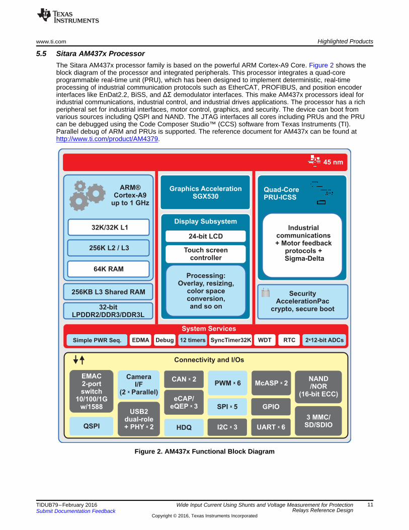
5.5 Sitara AM437x ProcessorThe Sitara AM437x processor family is based on the powerful ARM Cortex-A9 Core. Figure 2 shows theblock diagram of the processor and integrated peripherals. This processor integrates a quad-coreprogrammable real-time unit (PRU), which has been designed to implement deterministic, real-timeprocessing of industrial communication protocols such as EtherCAT, PROFIBUS, and position encoderinterfaces like EnDat2.2, BiSS, and ΔΣ demodulator interfaces. This make AM437x processors ideal forindustrial communications, industrial control, and industrial drives applications. The processor has a richperipheral set for industrial interfaces, motor control, graphics, and security. The device can boot fromvarious sources including QSPI and NAND. The JTAG interfaces all cores including PRUs and the PRUcan be debugged using the Code Composer Studio™ (CCS) software from Texas Instruments (TI).Parallel debug of ARM and PRUs is supported. The reference document for AM437x can be found athttp://www.ti.com/product/AM4379.
Figure 2. AM437x Functional Block Diagram

PRU1 Core(12KB Program)
PRU-ICSS1
PRU0 Core(12KB Program)
Data Mem0(8KB)
Data Mem1(8KB)
Shared RAM(32KB)
eCAP0
MII0_RT
IEP
UART0
CFG
32-B
it Inte
rconnect B
us
SPAD
EGP IO MPY/MAC
EGP
INTC
PRU1 Core(4KB Program)
PRU-ICSS0
PRU0 Core(4KB Program)
Data Mem0(4KB)
Data Mem1(4KB)
eCAP0
MII0_RT
IEP
UART0
CFG
32-B
it Inte
rconnect B
us
INTC
Interface/OCPSlave port
Interface/OCPMaster port
Interface/OCPMaster port
EGP IO
EGP IO
MPY/MAC
MPY/MAC
MPY/MAC
Highlighted Products www.ti.com
12 TIDUB79–February 2016Submit Documentation Feedback
Copyright © 2016, Texas Instruments Incorporated
Wide Input Current Using Shunts and Voltage Measurement for ProtectionRelays Reference Design
5.5.1 PRU-ICSSThe programmable real-time unit (PRU-ICSS) is a separate processing unit from the ARM core. The PRUcan operate independent of the ARM core after initialization. Also, the PRU is clocked independently forgreater efficiency and flexibility and can be used for offloading tasks from ARM. Alternatively, the PRU-ICSS can be used to implement additional peripheral interfaces and real-time protocols such as EtherCAT,PROFINET, EtherNet/IP, PROFIBUS, Ethernet Powerlink, Sercos3, EnDat2.2, and ΔΣde-modulator. The PRU core runs at a 200-MHz frequency and each PRU instruction takes 5 ns toexecute. This feature makes the PRU perfect for implementing real-time communication and controlsystems. Each PRU core has its own instruction and data memory, has access to all parts of a system-on-chip (SoC), has access to all pins, and can talk to all memories and I/Os except the ARM CPU memory,interrupt ARM, and receive events from ARM. The PRU can interact with other processors as defined bythe firmware loaded into instruction memory. Two ICSS blocks (each with two PRU cores), namely ICSS0and ICSS1, are available for industrial Ethernet and motor-side communication. The block diagram of bothPRUs is shown in Figure 3. For more details on PRU-ICSS, refer to the AM437x ARM Cortex-A9Processors Technical Reference Manual.
Figure 3. PRU-ICSS Block Diagram

www.ti.com Highlighted Products
13TIDUB79–February 2016Submit Documentation Feedback
Copyright © 2016, Texas Instruments Incorporated
Wide Input Current Using Shunts and Voltage Measurement for ProtectionRelays Reference Design
5.5.1.1 ΔΣ Decimation FilterΔΣ Sinc3 filtering is achieved by the combination of PRU hardware and firmware. PRU hardware provideshardware integrators that do the accumulation part of Sinc3 filtering, while the differentiation part is donein firmware. In the following topic, the filter implementation is explained for Sinc3 implementation;however, the same method can be used to implement other filtering.
Integration (PRU Hardware)Both ICSS0 and ICSS1 implement the integrators of the ΔΣ demodulators in the Enhanced GeneralPurpose Input Output (EGPIO) peripheral of the PRU. The integrator serves to count the number of 1s perclock event. Each channel has three cascaded counters, which are the accumulators for the Sinc3 filter.Each counter is 24 bits, giving a maximum count of 16,777,215. Each channel has a free-running rolloverclock counter. This sample counter updates the count value on the effective clock event for that channel.Each channel also contains a programmable counter compare block and the compare register has a sizeof 8 bits. However, the minimum value is 4 and maximum value is 202 because of the 24-bit accumulator.When the sample counter compare value has been reached, the shadow register copy is updated and theshadow register copy flag is set.
Features of the integrators in PRUs EGPIO:• Up to nine channels with concurrent counting• Flexible clock source configuration for each channel; option of independent clock source for each
channel or one clock source for three channels• Programmable, 8-bit sample counter compare register; used to set the OSR of Sinc3 filter• Three 24-bit cascaded counters per channel for accumulation, only Sinc3 and Sinc2 modes supported• Common channel enable (all channels are active or none are)
Figure 4 shows the implementation of an integrator with an ICSS-PRU.

CaptureSync acc1 acc2 acc3
Mux
Sample counter
Counter compare (min=4 and max=202)
Shadow register
Note: Note:
SD_IN
CLK_IN
Shadow register copy flag
CLK event
All acc are simple 24 bit adders
acc1 input is 1-bit
acc2 and acc3 inputs are 24-bit, rollover will occur at 0xff_ffff
Example: if acc2 = 0x10 and acc3 = 0xff_ffff, next clk_event will have acc3 = 0x0_000f
Every rising edge of CLK_OUT then
acc1 = acc1 + sd_sync
acc2 = acc2 + acc1
acc3 = acc3 + acc2
sample_count = sample_count +1
1) if ( over_sample_counter = over_sample_size)
then
Update shadow copy
set shadow_update_flag
reset over_sample_counter
2) snoop is optional method to read acc2 or acc3 directly
3) when sample_counter_select = 1 then
sample_count is read, if snoop = 1 then
direct read of active counter
Highlighted Products www.ti.com
14 TIDUB79–February 2016Submit Documentation Feedback
Copyright © 2016, Texas Instruments Incorporated
Wide Input Current Using Shunts and Voltage Measurement for ProtectionRelays Reference Design
Figure 4. Integrator Block Diagram in ICSS-PRU

RegisterRegister Register RegisterDN0
CN2 CN4
DN1 DN2 DN3 DN4 DN5
CN3 CN5
Output of ACC of integrator
Filter calculations (OSR=16, for Sinc3)
Circular buffer in shared RAM
Software comparator
To DGIO
Output of ACC of integrator
Filter calculations (OSR=128, for
sinc3)
www.ti.com Highlighted Products
15TIDUB79–February 2016Submit Documentation Feedback
Copyright © 2016, Texas Instruments Incorporated
Wide Input Current Using Shunts and Voltage Measurement for ProtectionRelays Reference Design
Differentiation (PRU Firmware)An overview of the firmware functions is shown in Figure 5. The firmware functions mainly consist of a setof different equations, referred to as the filter calculations. This firmware function is repeated for eachchannel. There are two data paths per channel shown in the firmware function: One path does a Sinc3decimation part of the filter calculation at a higher OSR used for accuracy and the other path is at a lowerOSR used to quickly respond to short-circuit conditions. The results of the higher OSR filter calculation areused by the application software. The digital value obtained with this filter is copied to a circular buffer of126 samples and the beginning of the buffer contains a write pointer that points to the latest sample in thebuffer.
The lower OSR filter is a parallel data path to the higher OSR filter. The output of the lower OSR filter iscompared with a threshold value in the PRU firmware. If the threshold is exceeded, the PRU indicates thisevent on a general purpose input/output (GPIO) pin with a signal transitioning from low to high. This pathis faster to calculate the result as it uses a smaller OSR; therefore, the path is used for input faultdetection. The OSR is configurable in both data paths.
Figure 5. Firmware Functions Overview
The implementation within the filter calculation block of Figure 5 is shown in Figure 6. Figure 6 is thedifferentiation, or the delta part, of the Sinc3 filter. The filter for both the high OSR filter and low OSR filteris of the same type.
Figure 6. Sinc3 Filter Differentiation Implementation in PRU

Highlighted Products www.ti.com
16 TIDUB79–February 2016Submit Documentation Feedback
Copyright © 2016, Texas Instruments Incorporated
Wide Input Current Using Shunts and Voltage Measurement for ProtectionRelays Reference Design
The calculation done in PRU to implemented the differentiation block is given here:
dn1 = dn0cn3 = dn0 – dn1dn3 = cn3cn4 = cn3 – dn3dn5 = cn3cn5 = cn4 – dn5dn5 = cn4cn5 = cn4 – dn5
‘dn0’ is the accumulated value for Sinc3 filter. This value is read from PRU hardware explained above.’cn5’ is the conversion result of the ΔΣ Sinc3 filtered. Other values are initialized to zero in the beginning.
The sample counter compares register sets up the OSRs of the filters. The shadow register copy flag isused to initiate the filter calculation and the shadow register copy flag is generated when the samplecounter overflows when it is equal to the sample counter compare register. However, because there isonly one flag per channel, the sample counter compare register is set up for the lower OSR. The higherOSR filter calculation is done by decimating the shadow register copy flag, which is done by a softwarecounter.
For example, for a lower OSR of 16 and a higher OSR of 128, the sample counter compares register is 16(that is, the lower OSR). For the higher OSR filter, the filter calculation is done every eighth time theshadow copy flag is generated, resulting in an OSR of 128 as 16 × 8 = 128. This also implies that thehigher OSR has to be a multiple of the lower OSR.
The firmware can be modified to have a different OSR. Overcurrent detection can be modified to eitheruse Sinc2 or accumulator value of Sinc2 or Sinc3 based on the requirement.

1000pFC40DNP
11
22
1A
1A
2A
2A
0.0007 OHM
R42
WSLP2726L7000FEA-ND
GND_USH
S
0
R57DNP
0R74
J4
LAMA2-14-QY
J5
LAMA2-14-QY
www.ti.com Getting Started
17TIDUB79–February 2016Submit Documentation Feedback
Copyright © 2016, Texas Instruments Incorporated
Wide Input Current Using Shunts and Voltage Measurement for ProtectionRelays Reference Design
6 Getting Started
6.1 Signal Conditioning for Current and Voltage Input
6.1.1 Isolated Current MeasurementA shunt is used to measure the input current instead of a conventional current transformer.
Shunt selection:The TIDA-00738 design can measure a current range of 0.1 A to 40 A (or 60 A). The shunt value andwattage are both important to minimize power dissipation across the shunt, which is mounted on theboard. This design uses a 0.7-mΩ shunt (see Figure 7). Table 5 summarizes the power loss for theselected shunt value.
Table 5. VA Drop Across Shunt
SHUNT VALUE CURRENT RANGE VOLTAGE DROP ACROSS SHUNT
0.7 mΩIMIN IMAX VSHMIN VSHMAX at 60 A
0.1 A 40 A (or 60 A) 70 µV 42 mV
NOTE: The expected nominal burden at In is < 0.1 VA at In = 1 A.
Figure 7. Onboard Shunt
Gain amplifier configuration:The following Table 6 shows the voltage input to the modulator, which is based on the configured gain.
Table 6. Voltage Input (Current Output) to Modulator
GAIN CURRENT SHUNT ±50-mV MODULATOR INPUTX 12.5 0.1 A to 4 A 0.7 mΩ 0.875 mVRMS to 35 mVRMS
X 0.8 2 A to 40 A (or 60 A) 0.7 mΩ 1.12 mVRMS to 22.4 mVRMS (or 33.6 mVRMS)

10.0R36
DNP
1000pFC37
806R40
1
3
2
D10BAT54SWT1G
1.00k
R37
GND_USH
VAN- 0R39
VAN+
0R38
VAN-
0.1µFC32DNP
GND_USH
0R68
0.1µF
C83
0.1µF
C84
GND_USH
GND_USH
1.00k
R67DNP
806R66DNP
VAN+
TP13
TP15
4
3
2
1
5
V+
V-
U15OPA188AIDBVR
1
3
2D11BAT54SWT1G
806
R44
GND_USH
VAN-
Shunt_H
0R46
0.1µF
C42
GND_USH
VAN+10.0kR47
0R45
0.1µFC36
GND_USH
VAN-
0.1µFC46DNP
11.0R48
DNP
GND_USH
1000pFC45
0R65806
R64DNP
10.0kR63DNP
VAN+
TP12
4
3
2
1
5
V+
V-
U10
OPA188AIDBVR
Getting Started www.ti.com
18 TIDUB79–February 2016Submit Documentation Feedback
Copyright © 2016, Texas Instruments Incorporated
Wide Input Current Using Shunts and Voltage Measurement for ProtectionRelays Reference Design
Figure 8 shows a schematic of the modulator with a high-gain amplifier input is linear that can be used upto 4 A. Figure 9 shows a schematic of the modulator with a low-gain amplifier input that can be used from4 A to 40 A (or 60 A).
Figure 8. High-Gain Amplifier Stage
Figure 9. Low-Gain Amplifier Stage
NOTE: The gain resistor values have been chosen based on accuracy testing performed on thewide current input. Any change in the value must be tested before implementing in thedesign.
GND_PH
2.40k
1
3
2
D9BAT54SWT1G
-2.5V_PH
4
3
2
1
5
V+
V-
U6OPA188AIDBVR
0.1µFC29
GND_PH
0.1µFC23
GND_PH
-2.5V_PH10.0R19
DNP
0.1µFC28DNP
100kR20
DNP
GND_PH
0.01µFC22DNP
VANP+
VANP+
0R71
0R81
0R70
0R82DNP
0R83DNP
GND_PH
TP14
TP
8
TP7
GND_PH
1
2
J1
ED120/2DS
332k
R14
332k
R15
332k
R16
332k
R17
2.40kR9
DNP1.02kR8
332k
R13
0
R7
0
R62
Neutral
0.01µFC22DNP
0R71
TP6
( )OUT
MAX _PK OUT
VR2 1.66 M
V V
R2 0.978 k
³ ´ W-
³ W
www.ti.com Getting Started
19TIDUB79–February 2016Submit Documentation Feedback
Copyright © 2016, Texas Instruments Incorporated
Wide Input Current Using Shunts and Voltage Measurement for ProtectionRelays Reference Design
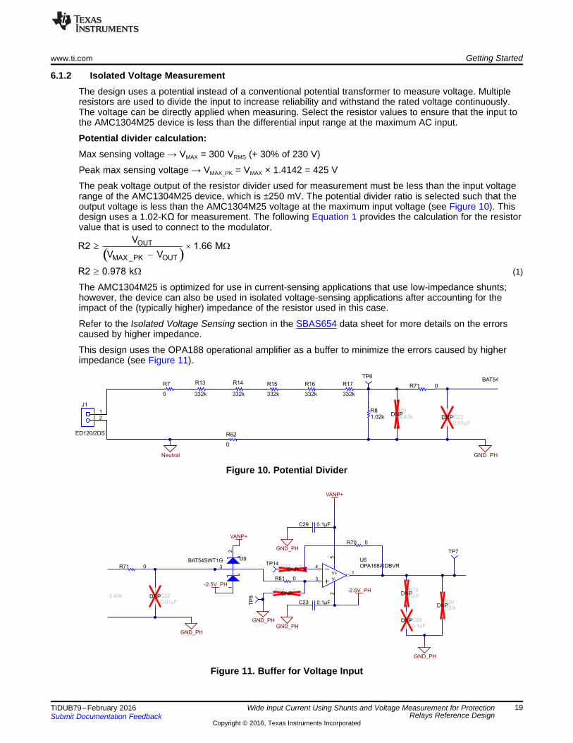
6.1.2 Isolated Voltage MeasurementThe design uses a potential instead of a conventional potential transformer to measure voltage. Multipleresistors are used to divide the input to increase reliability and withstand the rated voltage continuously.The voltage can be directly applied when measuring. Select the resistor values to ensure that the input tothe AMC1304M25 device is less than the differential input range at the maximum AC input.
Potential divider calculation:Max sensing voltage → VMAX = 300 VRMS (+ 30% of 230 V)
Peak max sensing voltage → VMAX_PK = VMAX × 1.4142 = 425 V
The peak voltage output of the resistor divider used for measurement must be less than the input voltagerange of the AMC1304M25 device, which is ±250 mV. The potential divider ratio is selected such that theoutput voltage is less than the AMC1304M25 voltage at the maximum input voltage (see Figure 10). Thisdesign uses a 1.02-KΩ for measurement. The following Equation 1 provides the calculation for the resistorvalue that is used to connect to the modulator.
(1)
The AMC1304M25 is optimized for use in current-sensing applications that use low-impedance shunts;however, the device can also be used in isolated voltage-sensing applications after accounting for theimpact of the (typically higher) impedance of the resistor used in this case.
Refer to the Isolated Voltage Sensing section in the SBAS654 data sheet for more details on the errorscaused by higher impedance.
This design uses the OPA188 operational amplifier as a buffer to minimize the errors caused by higherimpedance (see Figure 11).
Figure 10. Potential Divider
Figure 11. Buffer for Voltage Input

+3.3V_DVDD
0.1µF
C43
DGND10.0R41
DOUTP_CH_U
CLKP_CH_U
DGNDGND_USH
0R55
GND_USH
0.1µFC41
0.1µFC38
+5.0V_USH
0R56
10µFC72
0R43DNP
GND_USH
GND_USH
+3.3V_DVDD
0.1µF
C34
DGND
10.0R33DOUTP_CH_V
CLKP_CH_V
GND_USH
0R58
GND_USH
0.1
µF
C33
0.1µFC30
+5.0V_USH
0R59
10µFC73
0R35DNP
GND_USH DGND
2.2µFC44
2.2µFC35
100
0oh
m
L14
10
00
ohm
L9
0.1
µF
C39
1000
ohm
L11
0.1µF
C31
100
0oh
m
L8
NC1
VINP2
VINN3
NC4
NC5
LDO_IN6
AVDD7
AGND8
DGND9
NC10
DOUT11
NC12
CLKIN13
DVDD14
NC15
DGND16
U8
AMC1304M05DWR
NC1
VINP2
VINN3
NC4
NC5
LDO_IN6
AVDD7
AGND8
DGND9
NC10
DOUT11
NC12
CLKIN13
DVDD14
NC15
DGND16
U9
AMC1304M05DWR
Getting Started www.ti.com
20 TIDUB79–February 2016Submit Documentation Feedback
Copyright © 2016, Texas Instruments Incorporated
Wide Input Current Using Shunts and Voltage Measurement for ProtectionRelays Reference Design
Potential divider selection:Multiple resistors have been used to divide the input voltage to a ±250-mV input. Using multiple resistorsincreases the reliability. The number of resistors to use depends on the application and can be optimizedafter testing the product or system for conformance based on intelligent electronic device (IED) standards.
6.2 Isolated ΔΣ Modulators
6.2.1 AMC1304M05 ΔΣ Modulator for Current MeasurementThe input of the AMC1304M05 has been optimized for connecting directly to a shunt. The unique, low-input voltage range of the ±50-mV device reduces power dissipation through the shunt while supportingAC and DC measurement. The following schematics in Figure 12 show the use of two modulators formeasuring wide input current. The modulators provide reinforced isolation and a CMOS digital interface.
On the high side, the modulator is supplied by an integrated LDO regulator, which allows an unregulatedinput voltage between 4 V and 18 V (LDOIN). Both modulators share a common power supply.
Figure 12. Modulators for Current Measurement

10µFC68
10µFC67
+6V_USH
-6V_USH
D11
VCC2
D23
GND4
GND5
U13
SN6501DBV
20V
D17
MBR0520L
20V
D16
MBR0520L
1000pFC59DNP
GND_USH
GND_USH
0.1µFC54
0.1µFC56
0.1µFC57
+5V_CNTL
DGND
DGND
DGND
DGND
22µFC58
1 6
2 5
3 4
T2
750342271
+5V_CNTL
NC1
VINP2
VINN3
NC4
NC5
LDO_IN6
AVDD7
AGND8
DGND9
NC10
DOUT11
NC12
CLKIN13
DVDD14
NC15
DGND16
U5
AMC1304M25DW
+3.3V_DVDD
TP2
0.1µF
C25
DGND
10.0R10DOUTP_U_PH
CLKP_U_PH
DGND
0R11
GND_PH
GND_PHGND_PH
GND_PH
0.1µF
C210.1µFC19
+5.0V_PH
0R61
10µF
C76
0R60DNP
2.2µFC24
100
0oh
m
L51
000
ohm
L17
0.1
µF
C20
0R80
www.ti.com Getting Started
21TIDUB79–February 2016Submit Documentation Feedback
Copyright © 2016, Texas Instruments Incorporated
Wide Input Current Using Shunts and Voltage Measurement for ProtectionRelays Reference Design
6.2.2 AMC1304M25 ΔΣ Modulator for Voltage MeasurementThe modulator used to measure voltage has a ±250-mV input voltage range (see Figure 13). The powersupply to the voltage modulator is isolated from the current measurement modulators.
Figure 13. Modulator for Voltage Measurement
6.3 Isolated Power Supply
6.3.1 Current MeasurementA transformer driver is used to generate the required isolated DC voltage output for measuring current andvoltage (see Figure 14). This design implements two separate drivers to generate the power supply for theAFE. The design uses an isolation transformer with a 1.64:1 turns ratio to generate ±6 V. The ±6 V isregulated using LDOs to generate the required DC power supply rails.
Figure 14. Isolated Power Supply for Current Measurement

4.7µFC66
10µFC6510µF
C64
GND_USHGND_USH
GND_USH
0.1µFC63
0.1µFC60
0.01µFC62
0.01µFC61 GND_USH
-6V_USH -2.5V_USH
1.20kR52
Green
A2
C1
D18
GND_USH
TP3
10µFC69
0.1µFC53
GND_USH
+6V_USH
3.9kR49
4.7µFC52
0.1µFC55
GND_USH
+2.5V_USH
1.20kR53
Green
A2
C1
D14
GND_USH
1000 ohm
L16
GND_USH
3.9V
D15MMSZ5228B-7-F
3.9V
D19
MMSZ5228B-7-F
11.3kR51
10.2kR50
IN1
OUT5
GND2
NC4
EN3
U12
TPS70925DBVR
32.4kR69
DNP
TP5
OUT1
FB2
NC
3
GN
D4
EN5
NR
/SS
6
DNC7
VIN8
TP
AD
9
U14
TPS7A3001DGNR
10µFC70
0.1µFC51
GND_USHGND_USH
GND_USH
4.7µFC50
10µFC49
GND_USH
0.1µFC71
GND_USH
+5.0V_USH
+6V_USH
1.20kR54
Green
A2
C1
D13
GND_USH
6.2V
21
D12
1000 ohm
L15
TP4
GN
D1
NC
5
NC
4
OU
T3
IN2
U11TLV70450DBV
Getting Started www.ti.com
22 TIDUB79–February 2016Submit Documentation Feedback
Copyright © 2016, Texas Instruments Incorporated
Wide Input Current Using Shunts and Voltage Measurement for ProtectionRelays Reference Design
6.3.1.1 +5 V and ±2.5 V for CurrentThe following voltages are used to operate the AFE:• +5 V for modulators• +5 V or +2.5 V and –2.5 V for op amp
The output of the transformer driver is regulated using the LDOs in the following Figure 15 and Figure 16.The power supply outputs in both figures have protection against overvoltage and electrostatic discharge(ESD).
Figure 15. +5-V Supply for Modulators
Figure 16. ±2.5-V Supply for Op Amp
NOTE: 2.5 V is optional and is not required for use in this design.

10µFC79
0.1µFC10
GND_PHGND_PH
GND_PH
4.7µFC8
10µFC7
GND_PH
0.1µFC9
GND_PH
+5.0V_PH
1.20kR4
Green
A2
C1
D5
GND_PH
6.2V
21
D4
+6V_PH
GN
D1
NC
5
NC
4
OU
T3
IN2
U3TLV70450DBV
1000 ohm
L2
TP19
10µFC12
10µFC4
+6V_PH
-6V_PH
20V
D3
MBR0520L
20V
D6
MBR0520L
GND_PH
GND_PH
0.1µFC11
0.1µFC6
0.1µFC13
+5V_CNTL
DGND
DGND
DGND
1000pFC15DNP
1 6
2 5
3 4
T1
750342271
DGND
22µFC14
+5V_CNTL
D11
VCC2
D23
GND4
GND5
U2
SN6501DBV
www.ti.com Getting Started
23TIDUB79–February 2016Submit Documentation Feedback
Copyright © 2016, Texas Instruments Incorporated
Wide Input Current Using Shunts and Voltage Measurement for ProtectionRelays Reference Design
6.3.2 Voltage MeasurementThe isolated power supply design is similar to the current measurement block. The power supply outputsshown in Figure 17 have protection against overvoltage and ESD.
The following voltages are used to operate the AFE:• +5 V for modulator• +5 V or +2.5 V and –2.5 V for op amp
The output of the transformer diver is regulated using the LDOs in the following Figure 17.
Figure 17. Isolated Power Supply for Voltage Measurement
6.3.2.1 +5 V and ±2.5 V for VoltageThe following Figure 18 and Figure 19 show the LDOs used to generate the power supply for the voltagemodulators.
Figure 18. +5 V for Voltage Modulator
DGND
+3.3V_DVDD+5V_CNTL
1
2
3
J3
850-10-003-10-001000
4.7µFC82
10µFC8110µF
C80
0.1µFC5
0.1µFC2
OUT1
FB2
NC
3
GN
D4
EN5
NR
/SS
6
DNC7
VIN8
TP
AD
9
U1
TPS7A3001DGNR
0.01µFC3
0.01µFC1
-2.5V_PH
1.20kR2
Green
A2
C1
D1
TP1
10µFC78
0.1µFC18
3.9kR6
4.7µFC16
0.1µFC17
+2.5V_PH
1.20kR5
Green
A2
C1
D7
1000 ohm
L1
3.9V
D8MMSZ5228B-7-F
3.9
V
D2
MMSZ5228B-7-F
11.3kR3
10.2kR1
GND_PH GND_PH GND_PH
GND_PH
GND_PH
GND_PH
GND_PH
GND_PH
+6V_PH
-6V_PH
GND_PH
32.4kR77
DNP
TP18
IN1
OUT5
GND2
NC4
EN3
U4
TPS70925DBVR
Getting Started www.ti.com
24 TIDUB79–February 2016Submit Documentation Feedback
Copyright © 2016, Texas Instruments Incorporated
Wide Input Current Using Shunts and Voltage Measurement for ProtectionRelays Reference Design
Figure 19. ±2.5-V Rails for Op Amp
6.3.3 Digital Power Supply ConnectorThe power supply can be applied externally to test the AFE functionality. The 3.3 V and 5 V can beapplied from an external DC power supply for testing (see Figure 20).
Figure 20. Test Connector for Applying 5- and 3.3-V Supply
1 2
3 4
5 6
7 8
9 10
11 12
13 14
15 16
17 18
19 20
21 22
23 24
25 26
27 28
29 30
31 32
33 34
35 36
37 38
39 40
41 42
43 44
45 46
47 48
49 50
51 52
53 54
55 56
57 58
59 60
J2
NRPN302PAEN-RC
+5V_CNTL+3.3V_DVDD
DGND DGND
CLK_INCLK_OUT 0R12
SD_DATA_IN0_SD_CLKOUTSD_DATA_IN1
SD2SD_DATA_IN3SD_DATA_IN4SD_DATA_IN5SD_DATA_IN6SD_DATA_IN7
SD8
DOUTP_CH_UDOUTP_CH_V
DOUTP_U_PH
SD0_CLKINSD_CLKIN
0R210R23
0R240R27
DOUTP_CH_U
DOUTP_CH_V
DOUTP_U_PH
0R280R310R320R34
0R18
CLKIN1
1G2
Y03
GND4
Y25
VDD6
Y37
Y18
U7
CDCLVC1104PW
0.1µFC26
0.1µFC27
0.1µFC74
600 ohm
L6
1µFC75
+3.3V_DVDD
DGND
CLK_OUT
1.0kR30
+3.3V_DVDDCLKP_CH_U
DGND
CLKP_CH_V
CLKP_U_PH100R22
100R29
100R25
100
R26
www.ti.com Getting Started
25TIDUB79–February 2016Submit Documentation Feedback
Copyright © 2016, Texas Instruments Incorporated
Wide Input Current Using Shunts and Voltage Measurement for ProtectionRelays Reference Design
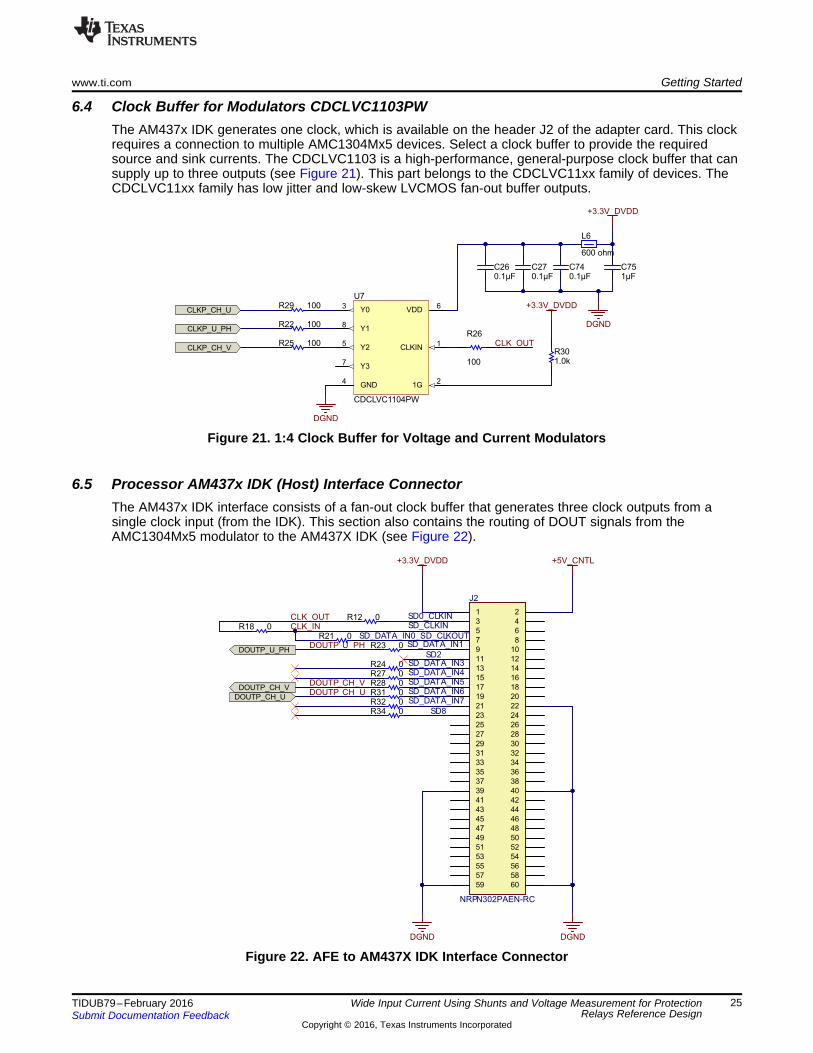
6.4 Clock Buffer for Modulators CDCLVC1103PWThe AM437x IDK generates one clock, which is available on the header J2 of the adapter card. This clockrequires a connection to multiple AMC1304Mx5 devices. Select a clock buffer to provide the requiredsource and sink currents. The CDCLVC1103 is a high-performance, general-purpose clock buffer that cansupply up to three outputs (see Figure 21). This part belongs to the CDCLVC11xx family of devices. TheCDCLVC11xx family has low jitter and low-skew LVCMOS fan-out buffer outputs.
Figure 21. 1:4 Clock Buffer for Voltage and Current Modulators
6.5 Processor AM437x IDK (Host) Interface ConnectorThe AM437x IDK interface consists of a fan-out clock buffer that generates three clock outputs from asingle clock input (from the IDK). This section also contains the routing of DOUT signals from theAMC1304Mx5 modulator to the AM437X IDK (see Figure 22).
Figure 22. AFE to AM437X IDK Interface Connector

AM437x Sitara ARM MPU
ICSS0
Connectivity
USBLCDMMC
CPGSW
SPII2C
UARTCAN
ICSS1
PRU0 PRU1 PRU0 PRU1
MDRV83133x PWM
OPA365to ADCs (3x I, 3x VBus)
3XGeneral Purpose
Processor
ARMCortex
A9
TXB0106PW X1x QEP
SN65HVD78 X1x EnDAT
M12
J 1x5
RT_MII signal connector
µSDI2C
EEPROMQSPIFlash
DDR3
GBit PHY
TLK105L
TLK105LXRJ45
XRJ45
RT_MII / CPGSW
RT_MII
1xCPGSWXRJ45
RX/TX/TX_enX
Expansion connector
DCAN_RX/TXX
Expansion connector
Expansion Connector
6x PWMSYNCO, SYNCI,
TRIPZONELATCH0/1PRU_SD3x QEP
PRU_EnDATADCsSPII2C
3V3, 5V, GND
Clock PMIC/ discrete solution
JTAG
Debug UART
Camera i/f
Power24V X
HVS882 X
TPIC2810 X
8x digitalI/O
SPI
I2C
LEDs
tripzone
Industrial LEDsGPIO
TI JTAG
XUSB XDS100v2or similar
JTAG
JTAG
UART
TX_EN, RX_DV,
EDIO
AM437x IDK (Industrial Development Kit)
Getting Started www.ti.com
26 TIDUB79–February 2016Submit Documentation Feedback
Copyright © 2016, Texas Instruments Incorporated
Wide Input Current Using Shunts and Voltage Measurement for ProtectionRelays Reference Design
6.6 AM437x IDKThe IDK is a self-contained evaluation module for the AM437x Sitara processor with onboard memory,power supplies, and power management. A 24-V input is stepped down using a buck converter togenerate all of the power rails required for the AM437x processors and memory. The 5 V and 3.3 Vgenerated are tapped to supply the other boards in the circuit. An onboard XDS100V2 is provided forJTAG connection using a micro-USB connector. The XDS100V2 device also provides a universalasynchronous receiver/transmitter (UART) connection to the Sitara processor, which enablescommunication with the GUI. The IDK supports various expansion headers interfacing with other boards.A 2×30-header is used to interface to the adapter card.
The AM437x IDK is an application development platform for evaluating the industrial communication andcontrol capabilities of Sitara AM4379 and AM4377 processors for industrial applications (see Figure 23).
Figure 23. AM437x IDK Block Diagram

I/O Expansion CAN Profibus PWM eQEP SPI And others
Onboard memory 1 GB of DDR3 64 MB of QSPI-NOR
(backside of the board)
2x Industrial Ethernet Ports For industrial Ethernet
protocols such as EtherCATor others
Uses TLK105L
µSD card slotExpansion forcode and storage
Ethernet PortGigabit
EnDat connectorFor motor positionfeedback control
JTAG connector20-pin cTI
Onboard camera2Mp CMOS module
24 V DC Power
1GHz Sitara AM437x ARM ®
&RUWH[- A9 processor
High performance CPU for user interface and control
Quad-Core PRU for industrial protocols
Micro USB (2.0) UART to AM437x XDS100v2
emulator support
Industrial I/O LED driver outputs Industrial inputs ADC
HeadereQEP
Motor connectorUp to 3-phase drive
Industrial Ethernet debug LEDs and test signals
www.ti.com Getting Started
27TIDUB79–February 2016Submit Documentation Feedback
Copyright © 2016, Texas Instruments Incorporated
Wide Input Current Using Shunts and Voltage Measurement for ProtectionRelays Reference Design
The AM437x IDK features:• Connectivity: The IDK supports many connectivity options used in motor drives like EtherCAT®, EnDat
2.2 BiSS, PROFINET, CANOpen, PROFIBUS®, POWERLINK, Ethernet/IP, SERCOS III, andIEC61850
• Position encoder interface• Three-phase motor driver• microSD card: used to store the application software• Onboard Isolated JTAG Emulation: the JTAG interface supported by the onboard XDS100V2 emulator
is used for a convenient interface with TI's Code Composer Studio™ (CCS) software. The XDS100V2also interfaces with the AM437x UART, which connects to the GUI.
• Multiple expansion headers: breakout for digital inputs and outputs (I/O), pulse width modulation(PWM), serial peripheral interface (SPI), and ΔΣ decimation filter
The following Figure 24 highlights the aforementioned features and more.
Figure 24. AM437x IDK
The firmware implements for four channels: 1, 5, 6, and 7. The firmware only implements four channelsbecause some of the pins used for ΔΣ demodulation have been allocated for other functions on the IDK. Acustom design can support up to nine channels of ΔΣ demodulators. A higher oversampling rate (OSR) of128 is used and must be a multiple of the lower OSR (for fault current processing).

SD_DATA_IN0_SD_CLKOUT
SD_DATA_IN1
SD_DATA_IN5
SD_DATA_IN6
ARM Shared memory
PRU
ICSS
SD
SD 1
SD 5
SD 6
TIDA-00738
Getting Started www.ti.com
28 TIDUB79–February 2016Submit Documentation Feedback
Copyright © 2016, Texas Instruments Incorporated
Wide Input Current Using Shunts and Voltage Measurement for ProtectionRelays Reference Design
6.7 Application Software DescriptionFigure 25 shows the interaction between the ARM, PRU, and ΔΣ modulator card.
Figure 25. Interaction Between ARM, ICSS, PRU, and TIDA-00738
The software for this design has been developed as a SYSBIOS CCS project. The SYSBIOS contains aStarterWare™ software library from TI for handling various peripherals on the AM437x. The purpose ofthe software is to set up the pinmux, start PRU execution, handle the UART port (available over USBthrough an onboard FTDI) to interface with the GUI in a host PC so the user can validate theAMC1304Mx5 performance, and configure the OSR and ΔΣ modulator clock frequency.
The software initially controls the setup of the pinmux for the ΔΣ clock, signal lines, and PRU digital I/Os.The software then Initializes the PRU1 of ICSS_L, loads the ΔΣ firmware onto its instruction memory, andstarts execution. Next, the UART is set up using StarterWare libraries. The AM437x device provides theclock for the ΔΣ modulator and the software configures the PRU to provide the required clock frequency.The GUI in the host PC can configure OSR. The software mostly functions like a client for the GUI andhandles the configuration of the PRU ΔΣ OSR accordingly. The software also controls the transfer ofsampled values through the UART so that the GUI can display the measured samples. Because the GUIrequires 16-bit signed data, a sample value is signed and the majority of significant 16 bits are extractedand then sent to the GUI.
6.7.1 Getting StartedThis software has been compiled from CCS. The SD card is loaded with two files: ‘app’, which is thegenerating executable binary, and 'mlo', the bootloader. On power up, the AM437x loads the applicationfrom the SD card located in the micro SD card slot on the IDK. For further details on creating these filesfrom the source code, consult the AM437x SYSBIOS Industrial SDK 02.00.00.02 User Guide [ 3].

www.ti.com GUI User's Guide
29TIDUB79–February 2016Submit Documentation Feedback
Copyright © 2016, Texas Instruments Incorporated
Wide Input Current Using Shunts and Voltage Measurement for ProtectionRelays Reference Design
7 GUI User's GuideThis section describes the functionality of the GUI for isolated current and voltage measurements.
7.1 Installing Run-Time EngineFollow these steps to download and install the LabVIEW™ run-time engine to use the IVIM Test Bench:1. Click on the link to install the LabVIEW Run-Time Engine 2010 SP1 (32-bit Standard RTE):
http://www.ni.com/download/labview-run-time-engine-2010-sp1/2292/en/2. Run LVRTE2010_SP1f5std.exe to install the LabVIEW 2010 SP1 Run-Time Engine (32-bit).3. Follow the installation wizard and complete the installation.
The installation files for the run-time engine are automatically extracted to a directory on disk. The installerdoes not remove the files after installing. To remove these files from the disk, note their location during theunzipping process.
7.2 Installing VISAFollow these steps to download and install the VISA driver to communicate with the device:1. Click the link to install the NI-VISA 5.0.3: http://www.ni.com/download/ni-visa-5.0.3/2251/en/2. Run the visa503full_downloader.exe.3. Follow the installation wizard and complete the installation.
GUI User's Guide www.ti.com
30 TIDUB79–February 2016Submit Documentation Feedback
Copyright © 2016, Texas Instruments Incorporated
Wide Input Current Using Shunts and Voltage Measurement for ProtectionRelays Reference Design
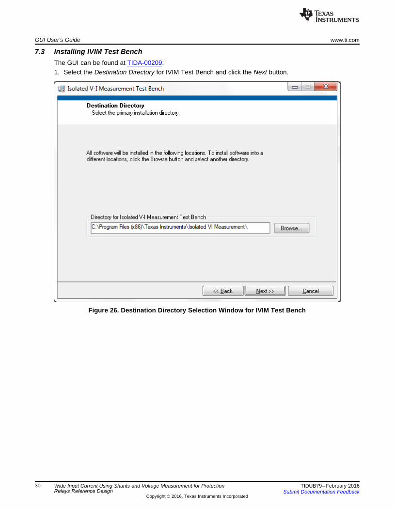
7.3 Installing IVIM Test BenchThe GUI can be found at TIDA-00209:1. Select the Destination Directory for IVIM Test Bench and click the Next button.
Figure 26. Destination Directory Selection Window for IVIM Test Bench

www.ti.com GUI User's Guide
31TIDUB79–February 2016Submit Documentation Feedback
Copyright © 2016, Texas Instruments Incorporated
Wide Input Current Using Shunts and Voltage Measurement for ProtectionRelays Reference Design
2. Figure 27 shows the list of files that will be added or modified with this installation. Click the Nextbutton.
Figure 27. List of Files Added or Modified With Installation
GUI User's Guide www.ti.com
32 TIDUB79–February 2016Submit Documentation Feedback
Copyright © 2016, Texas Instruments Incorporated
Wide Input Current Using Shunts and Voltage Measurement for ProtectionRelays Reference Design
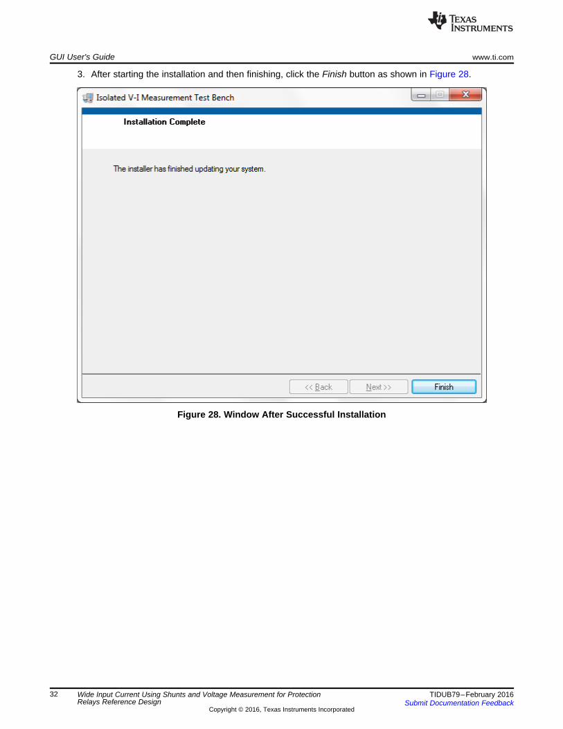
3. After starting the installation and then finishing, click the Finish button as shown in Figure 28.
Figure 28. Window After Successful Installation

www.ti.com GUI User's Guide
33TIDUB79–February 2016Submit Documentation Feedback
Copyright © 2016, Texas Instruments Incorporated
Wide Input Current Using Shunts and Voltage Measurement for ProtectionRelays Reference Design
7.4 Launching IVIM Test BenchFollow these steps to launch the IVIM Test Bench:1. Locate the IVIM Test Bench through any of these approaches:
• Desktop shortcut• Start menu shortcut• Installed folder location; the default location is:
C:\Program Files (x86)\Texas Instruments\Isolated VI Measurement\2. Double-click on the Isolated V-I Measurement.exe (Figure 29)
Figure 29. Isolated VI Measurement Folder Structure

GUI User's Guide www.ti.com
34 TIDUB79–February 2016Submit Documentation Feedback
Copyright © 2016, Texas Instruments Incorporated
Wide Input Current Using Shunts and Voltage Measurement for ProtectionRelays Reference Design
7.5 Mode SelectionThe Select a Mode dialog box pops up as the application is launched (Figure 30). Select Sitara and thecorresponding VISA resource name (the communication port number that appears when the AM437X IDKis connected to the computer).
Figure 30. Mode Selection
As soon as the user selects the mode, the GUI starts to initialize.
Figure 31. GUI Initialization
Proceed to use the GUI after the initialization completes.

www.ti.com GUI User's Guide
35TIDUB79–February 2016Submit Documentation Feedback
Copyright © 2016, Texas Instruments Incorporated
Wide Input Current Using Shunts and Voltage Measurement for ProtectionRelays Reference Design
7.6 IVIM PagesThe IVIM Test Bench has three pages:1. System Layout2. Config3. Graph
7.6.1 System LayoutThe System Layout page shows the block diagram with a description of the parts used in the isolatedcurrent and voltage measurement. Moving the mouse pointer over any of the blocks shows the descriptionof the same on the right side of the page with web links for reference. Refer to Figure 32.
Figure 32. System Layout
• Block Diagram: The block diagram gives the detailed description of the parts used for isolated voltageand current measurement.
• Part Name: This box displays the part name selected.• Description Box: This box displays a brief description about the part in the block diagram.• Web Link Box: This box displays the web reference of the part.

GUI User's Guide www.ti.com
36 TIDUB79–February 2016Submit Documentation Feedback
Copyright © 2016, Texas Instruments Incorporated
Wide Input Current Using Shunts and Voltage Measurement for ProtectionRelays Reference Design
7.7 Config PageThis page allows the user to configure the ΔΣ filter parameters.
Figure 33. Config Page
• Motor Current: This option contains the settings for three channels to be configured for respectivephase current.
• Inverter Voltage: This option contains the settings for three channels to be configured for respectivephase voltage.
• DC Link Voltage: This option contains the setting for a channel to be configured for DC Link voltage.• Set: This button sets the configured settings for the corresponding row.• Set All: This button sets the configured value for all channels.• Default All: This button sets the default values for all channels.• Load: This button loads the values for each parameter form the file specified in the in the path
dialog box.• Configuration Summary: This option displays the modulated frequency for each of the channels.

www.ti.com GUI User's Guide
37TIDUB79–February 2016Submit Documentation Feedback
Copyright © 2016, Texas Instruments Incorporated
Wide Input Current Using Shunts and Voltage Measurement for ProtectionRelays Reference Design
7.7.1 Setting Oversampling Rate• Oversampling Rate: Enter the desired OSR for the Sinc filter. The oversampling rate can be selected
from the list.
Figure 34. OSR Selection
• Modulator Frequency: This is a calculated value, which is the frequency of the clock signal given to theΔΣ modulator. The modulator frequency depends on the PWM frequency and oversampling rate.Considering two samples are required for every PWM period, the required sampling rate is twice thePWM frequency. The modulator frequency is calculated as 2 × (PWM Frequency) × OSR. The twosamples requirement is a suggestion; however, it can be changed depending on the applicationrequirement. The modulator frequency is limited to 20 MHz.
• Input Frequency: Enter the frequency of the input clock or crystal on the board. The GUI uses thisvalue along with the required modulator frequency to calculate the PLL configuration registers andclock dividers on the board.
7.7.2 Setting Filter TypeSelect the desired filter type for each channel from the list shown in Figure 35:
Figure 35. Channel Filter Type
7.7.3 Setting Default ValueEach channel can be configured to their default values using the Default button provided for each channel.The user can also use the Default All button to set default values to all the channels.

GUI User's Guide www.ti.com
38 TIDUB79–February 2016Submit Documentation Feedback
Copyright © 2016, Texas Instruments Incorporated
Wide Input Current Using Shunts and Voltage Measurement for ProtectionRelays Reference Design
7.7.4 Configuration SummaryThe configuration summary box gives the calculated modulator frequency for each channel. Themodulator frequency has a limit of 5 MHz to 20 MHz. When the set values exceed the limit, the values arecoerced and the summary box indicates the error with a notification, as Figure 36 shows.
Figure 36. Configuration Summary
7.7.5 Loading Default Values FileSelect the default values file using the available path control. Click on the Load button to load the settingsto the user interface.
Figure 37. Load Default Values File
7.7.6 Setting ConfigurationSet the final channel configuration by using the Set buttons provided with each channel or the Set Allbutton to set the configurations of all the channels. When the Set All button is pressed, all the settings inthe Config page are sent to the MCU as previously selected.

www.ti.com GUI User's Guide
39TIDUB79–February 2016Submit Documentation Feedback
Copyright © 2016, Texas Instruments Incorporated
Wide Input Current Using Shunts and Voltage Measurement for ProtectionRelays Reference Design
7.8 Graph Display for Measured ParametersThe Graph page is the result display and processing page (Figure 38). The captured values are displayedas graphs in this page in either the time domain or frequency domain.
Figure 38. Graph Page
• Graph Config: This pane sets the trigger modes and selects the waveforms to display.• Waveform Parameter: This pane displays the parameters of the selected waveform.• Graph Pane: The captured data is plotted in the form of a graph in this pane.• Error Indicators: The graph page has eight indicators to detail the error. The Clear Alarm button erases
the indications.• Process from File: This button plots the data from the file in a graph.

GUI User's Guide www.ti.com
40 TIDUB79–February 2016Submit Documentation Feedback
Copyright © 2016, Texas Instruments Incorporated
Wide Input Current Using Shunts and Voltage Measurement for ProtectionRelays Reference Design
7.8.1 Setting Trigger Channel and Capture TimeThe trigger channel can be set using the Trigger Channel control. Select any of the channels available.Set the trigger threshold of the selected channel in the Trigger Threshold control. The trigger channel andtrigger threshold vales are sent to the target, where the target waits for the input on this channel to crossthe trigger threshold value.
Select the scale factor from the Scale Factor control to calculate the digital value corresponding to thetrigger threshold value (see Figure 39).
Set the capture time in milliseconds (ms) in the Capture Time control. The maximum value is 100 ms,which is limited because of the amount of memory reserved for buffering the samples. The GUI canrequest for more than 100 ms, but the data will be clipped because of rollover from the buffer pointerinside the firmware of Sitara.
Figure 39. Trigger Configuration
7.8.2 Selecting Waveform and Scale FactorThe waveform to be displayed and its corresponding scale factors can be selected from the Waveform 1and Waveform 2 control (see Figure 40). The scale factors are selected from their respective controls. Thescale factor here selects how the digital value received for the target corresponds to voltage or currentvalues on the waveform.
Figure 40. Waveform Settings

www.ti.com GUI User's Guide
41TIDUB79–February 2016Submit Documentation Feedback
Copyright © 2016, Texas Instruments Incorporated
Wide Input Current Using Shunts and Voltage Measurement for ProtectionRelays Reference Design
7.8.3 Selecting FilterThe Filters tab shows the post processing options that can be done by the GUI. Select the configurationfrom the Filters tab.
Figure 41. Filter Selection
The filter can be selected from the Type control.
Figure 42. Filter Type Selection
The filter characteristics can be selected using the Filter Type, High and Low Cutoff Freq, and Ordercontrols. The low-pass filter ignores the High Cuttoff Freq setting and the high-pass filter ignores the LowCutoff Freq filter setting.

GUI User's Guide www.ti.com
42 TIDUB79–February 2016Submit Documentation Feedback
Copyright © 2016, Texas Instruments Incorporated
Wide Input Current Using Shunts and Voltage Measurement for ProtectionRelays Reference Design
7.8.4 FFT Window SelectionFFT windows can be selected using the FFT-Window control in the Post Processing tab. This selectionaffects the FFT graph if the graph is selected to display FFT of the waveform captured (see Figure 43).
Figure 43. FFT Window Selection
7.8.5 Waveform Parameter DisplayThe parameters of the selected channel can be noted from the waveform page as in Figure 44.
Figure 44. Waveform Parameter Display

www.ti.com GUI User's Guide
43TIDUB79–February 2016Submit Documentation Feedback
Copyright © 2016, Texas Instruments Incorporated
Wide Input Current Using Shunts and Voltage Measurement for ProtectionRelays Reference Design
7.8.6 Data CaptureClick on the Capture button shown in Figure 45 to obtain the results.
Figure 45. Data Capture Button
Capture mode sends the corresponding settings to the target, retrieves the data for the time specified, anddisplays it in the graph once.
7.8.7 Selecting DomainSelect the graph domain using the control provided for each graph and the time or frequency domainusing the control as shown in Figure 46.
Figure 46. Graph Domain Selection

GUI User's Guide www.ti.com
44 TIDUB79–February 2016Submit Documentation Feedback
Copyright © 2016, Texas Instruments Incorporated
Wide Input Current Using Shunts and Voltage Measurement for ProtectionRelays Reference Design
7.8.8 WaveformsThe following waveforms in Figure 47 and Figure 48 show current waveforms for high-gain and low-gainmodulator paths.
Figure 47. Current Input Waveform at 60 Hz
Figure 48. 10-A Input at High-Gain Modulator (Saturated) and Low-Gain Modulator

www.ti.com GUI User's Guide
45TIDUB79–February 2016Submit Documentation Feedback
Copyright © 2016, Texas Instruments Incorporated
Wide Input Current Using Shunts and Voltage Measurement for ProtectionRelays Reference Design
7.9 Layout Guidelines• Modulator: Follow the layout design guidelines as recommended in the Layout section of the
AMC1304Mx5 datasheet (SBAS655).• Clock buffer: Follow the layout design guidelines as recommended in the Layout section of the
CDCLVC1104 datasheet (SCAS895).• Transformer driver for isolated power supplies: Follow the layout design guidelines as recommended in
the Layout section of the SN6501 datasheet (SLLSEA0).• Shunt: The current applied flows across the shunt and the current input terminal. Ensure proper copper
flow to reduce the heating of the board.
7.10 Future EnhancementsUse of a higher shunt value:Based on the application, if the design requires the use of a higher shunt, the gains of the amplifiers canbe adjusted to vary the gain.
Measuring a wider current range:The gain X 0.8 can be reduced further if the range of current to be measured is higher than 60 X In.
Configuring the design for a 5-A application:This design can be used in applications with a 5-A nominal current by reducing the shunt value andadjusting the gain of the amplifiers.

Connector J16
Connector J18Connector J18
Getting Started www.ti.com
46 TIDUB79–February 2016Submit Documentation Feedback
Copyright © 2016, Texas Instruments Incorporated
Wide Input Current Using Shunts and Voltage Measurement for ProtectionRelays Reference Design
8 Getting Started
8.1 EVM (IDK) InterfaceThe current inputs are connected using J4 and J5 terminals and the voltage input is connected usingconnector J1.
8.1.1 Connecting AFE and EVM (IDK)Table 7 shows the channels that are used for current and voltage measurement by the IDK.
Table 7. GUI Channels for Current and Voltage Measurement
ADC OUTPUT GUI CHANNEL SELECTEDHigh-gain stage AMC1304M05 output Channel 2Low-gain stage AMC1304M05 output Channel 3
Voltage measurement AMC1304M25 output Channel 6
NOTE: Only two channels of data can be analyzed by the GUI at a given time.
8.1.2 Program the IDKThe firmware required for interfacing the AMC437X IDK with the modulator is provided as executables.Two files are generated after compilation in the release folder of the IDK: 'app' and 'MLO'. Copy the appand MLO executables in the micro-SD card available in connector J19 of the IDK.
8.1.3 Interface With AM437X IDKFigure 49 shows how to connect the TIDA-00738 board to the AM437x IDK.
Align the connector J2 pin 1 on the TIDA-00738 board with the I/O expansion connector J16 pin 1 on theIDK. Press the J2 connector carefully in the I/O expansion connector J16 on the IDK while being cautiousof ESD and mechanical strength.
Figure 50 shows the power and USB connections. J12 is the power connection and J18 is the USBconnection.
Figure 49. Connecting TIDA-00738 Board to AM437x IDK Figure 50. Power and USB Connection

0.0019073 mV/count0.002724825 A/count
0.7 m=
W
( )( )( )( )
62.5 mV 62.5 mV0.0019073 mV/count
32767 32768
- -=
- -
www.ti.com Getting Started
47TIDUB79–February 2016Submit Documentation Feedback
Copyright © 2016, Texas Instruments Incorporated
Wide Input Current Using Shunts and Voltage Measurement for ProtectionRelays Reference Design
NOTE: The following steps are important to note before making any changes:• Ensure that the power to the AM437X IDK has been switched off• Be sure to insert the AFE connector into the correct position of the IDK
connector
8.1.4 Powering AM437x and TIDA-00738 AFE BoardsSet the power supply to 24-V DC with a current limit of 300 mA. Connect the DC input to the 24-V DCpower connector J12 on the AM437X IDK board. The light-emitting diodes (LEDs) on the TIDA-00738board must be ON. The current shown in the power supply should be around 200 mA.
8.1.5 AM437X IDK USB Interface With GUIConnect a USB cable between J18 and the GUI host computer to establish communication with theAM437X IDK.
8.1.6 Voltage and Current InputConnect a programmable current source at J5 (M – Current In) and J4 (L – Current Out). Connect aprogrammable voltage source at connector J1 (Pin 1 – Phase and Pin 2 Neutral).
8.2 Setting Up Scale Factor for Measurement
8.2.1 CurrentThe GUI collects samples from the AM437X IDK after performing the Sinc3 filtering with the specifiedOSR. The GUI computes the RMS values using the samples. The samples are scaled to mV or the inputvalues using a scaling factor. The modulator used for the current measurement is ±50 mV. The total full-scale range of the AMC1304M05 device is 62.5 mV to –62.5 mV. This range corresponds to a range of32767 to –32768 for a 16-bit result register.
Equation 2 shows the conversion factor for mV:
(2)
Converting mV to input current:This design uses a shunt value of 0.7 mΩ. The mV measured is converted to the input current asEquation 3 shows:
(3)
Because the high-gain stage provides an X 12.5 gain, the scale factor must be multiplied by 12.5. A high-gain modulator output is connected to channel 2 (GUI) of the AM437X IDK.
The scale factor for the high-gain stage channel 2 (GUI) is 0.000219621 A/ADC count.
The low-gain stage is connected to channel 3 (GUI) of the AM437X IDK. Because the low-gain stageprovides an X0.8 gain, the scale factor must be multiplied by 0.8. The scale factor for the low-gain stagechannel 3 (GUI) is 0.003380677 A/count.
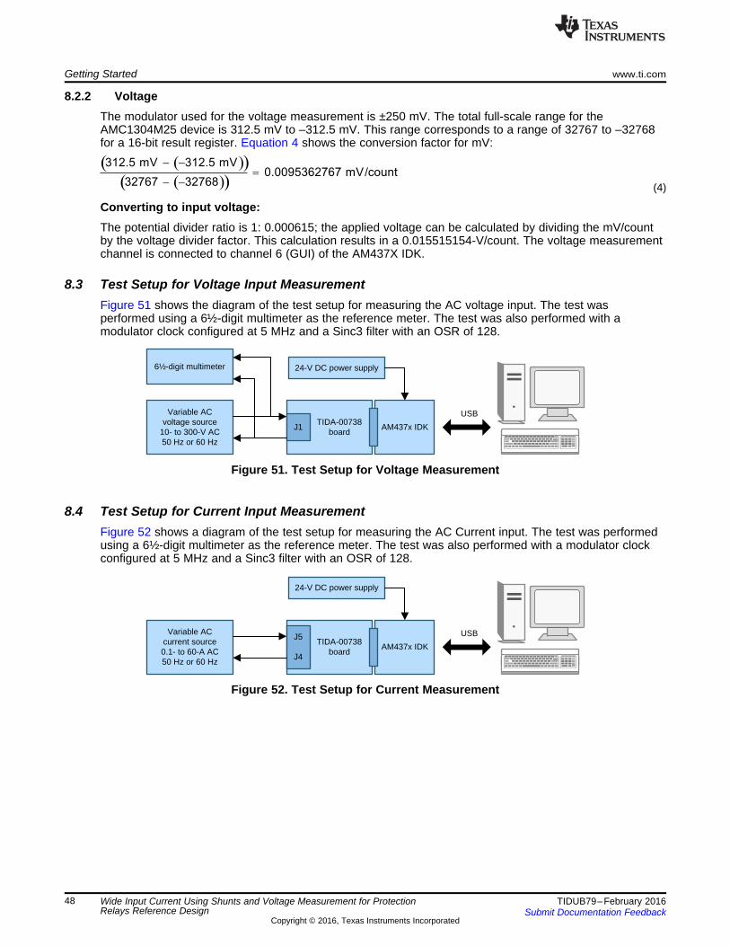
Variable ACcurrent source0.1- to 60-A AC50 Hz or 60 Hz
24-V DC power supply
TIDA-00738 board
J5
J4AM437x IDK
USB
6½-digit multimeter
Variable ACvoltage source
10- to 300-V AC50 Hz or 60 Hz
24-V DC power supply
TIDA-00738 board
J1 AM437x IDK
USB
( )( )( )( )
312.5 mV 312.5 mV0.0095362767 mV/count
32767 32768
- -=
- -
Getting Started www.ti.com
48 TIDUB79–February 2016Submit Documentation Feedback
Copyright © 2016, Texas Instruments Incorporated
Wide Input Current Using Shunts and Voltage Measurement for ProtectionRelays Reference Design
8.2.2 VoltageThe modulator used for the voltage measurement is ±250 mV. The total full-scale range for theAMC1304M25 device is 312.5 mV to –312.5 mV. This range corresponds to a range of 32767 to –32768for a 16-bit result register. Equation 4 shows the conversion factor for mV:
(4)
Converting to input voltage:The potential divider ratio is 1: 0.000615; the applied voltage can be calculated by dividing the mV/countby the voltage divider factor. This calculation results in a 0.015515154-V/count. The voltage measurementchannel is connected to channel 6 (GUI) of the AM437X IDK.
8.3 Test Setup for Voltage Input MeasurementFigure 51 shows the diagram of the test setup for measuring the AC voltage input. The test wasperformed using a 6½-digit multimeter as the reference meter. The test was also performed with amodulator clock configured at 5 MHz and a Sinc3 filter with an OSR of 128.
Figure 51. Test Setup for Voltage Measurement
8.4 Test Setup for Current Input MeasurementFigure 52 shows a diagram of the test setup for measuring the AC Current input. The test was performedusing a 6½-digit multimeter as the reference meter. The test was also performed with a modulator clockconfigured at 5 MHz and a Sinc3 filter with an OSR of 128.
Figure 52. Test Setup for Current Measurement

www.ti.com Test Data
49TIDUB79–February 2016Submit Documentation Feedback
Copyright © 2016, Texas Instruments Incorporated
Wide Input Current Using Shunts and Voltage Measurement for ProtectionRelays Reference Design
9 Test DataSampling rate:The modulator clock is 5 MHz and the OSR used is 128. The sampling rate is 39062.5 samples persecond (5 MHz / 128).
The AFE can be used to measure to measure the following:• Wide AC current input• Wide DC current input• Wide AC voltage input• Wide DC voltage input• Input frequency can be 50 Hz or 60 Hz
The single-ended measurement mode is used when measuring current and voltage.
Using a shunt provides the advantage of measuring AC or DC current. Similarly, using a resistor as thepotential divider provides the advantage of measuring AC or DC voltage.
The data from two channels can be collected for analysis at a given time. In the TIDA-00378 design, threemodulator inputs have been connected to the processor.
Test conditions for measuring voltage or current inputs:The number of samples used for the computation of RMS current is 60 ms or 100 ms (three to five cyclesat 50 Hz).
The number of samples used for the computation of RMS voltage is 100 ms (five cycles at 50 Hz).
Shunt value:The AFE has been tested for accuracy performance with 0.7 mΩ and 1 mΩ.
Choosing the shunt value:If the minimum current input to be measured within a specified accuracy is ≥ 100 mA, then 0.7 mΩ can beconsidered. For measuring lower currents, ≤ 50 mA, 1 mΩ is recommended.
Table 8 shows a summary of the performance tests with the TIDA-00738 board.
Table 8. Summary of Performance Tests
SERIAL NUMBER TEST DETAILS
1 Current measurementCurrent measurement at 50 Hz with 0.7- and 1-mΩ shuntsCurrent measurement at 60 Hz with 0.7-Ω shuntDC current measurement with 0.7-mΩ shunt
2 Voltage measurementAC voltage measurement at 50 Hz and 60 HzDC voltage measurement
3 Repeatability Repeatability testing—power cycling and long-term stability4 VA burden VA burden for current input

Test Data www.ti.com
50 TIDUB79–February 2016Submit Documentation Feedback
Copyright © 2016, Texas Instruments Incorporated
Wide Input Current Using Shunts and Voltage Measurement for ProtectionRelays Reference Design
9.1 Current Measurement
NOTE: The current input range used for testing the accuracy performance is based on a 1-A In. Foran improved accuracy performance at lower currents, populate R64 and R64.
Two modulators have been used to ensure that the wide current input is measured within a specifiedaccuracy.• A modulator with a X 12.5 gain (amplifier output gain) is used to measure 0.1 A to 4 A. The result was
monitored on channel 2 of the GUI.• A modulator with X 0.8 gain is used to measure 1 A to 40 A (or 60 A). The result was monitored on
channel 3 of the GUI.
The accuracy measurement was performed at the 50- and 60-Hz inputs.
9.1.1 Current Measurement at 50 Hz
Table 9. Current Measurement at 50-Hz Input, 60-ms Sampling, and 0.7-mΩ Shunt
INPUTCURRENT
EXPECTED mVINPUT TO HIGH-GAIN
MODULATORMEASURED %ERROR_Hg
EXPECTED mVINPUT TO LOW-
GAIN MODULATORMEASURED %ERROR_Lg
0.050 0.434 0.4381 0.9405 — — —0.075 0.651 0.6517 0.1105 — — —0.10 0.868 0.8687 0.0837 — — —0.20 1.736 1.7355 –0.0301 0.112 0.1125 0.45350.50 4.34 4.3430 0.0685 0.28 0.2805 0.17991.00 8.68 8.6902 0.1176 0.56 0.5606 0.10802.00 17.36 17.3823 0.1286 1.12 1.1221 0.18543.00 26.04 26.0766 0.1407 1.68 1.6828 0.16864.00 34.72 34.7719 0.1496 2.24 2.2439 0.17435.00 43.4 43.3390 –0.1406 2.8 2.8049 0.17576.00 52.08 47.6988 –8.4124 3.36 3.3659 0.176310.00 — — — 5.6 5.6098 0.175320.00 — — — 11.2 11.2206 0.183730.00 — — — 16.8 16.8289 0.172140.00 — — — 22.4 22.4193 0.086050.00 — — — 28 28.0066 0.023760.00 — — — 33.6 33.6205 0.0609
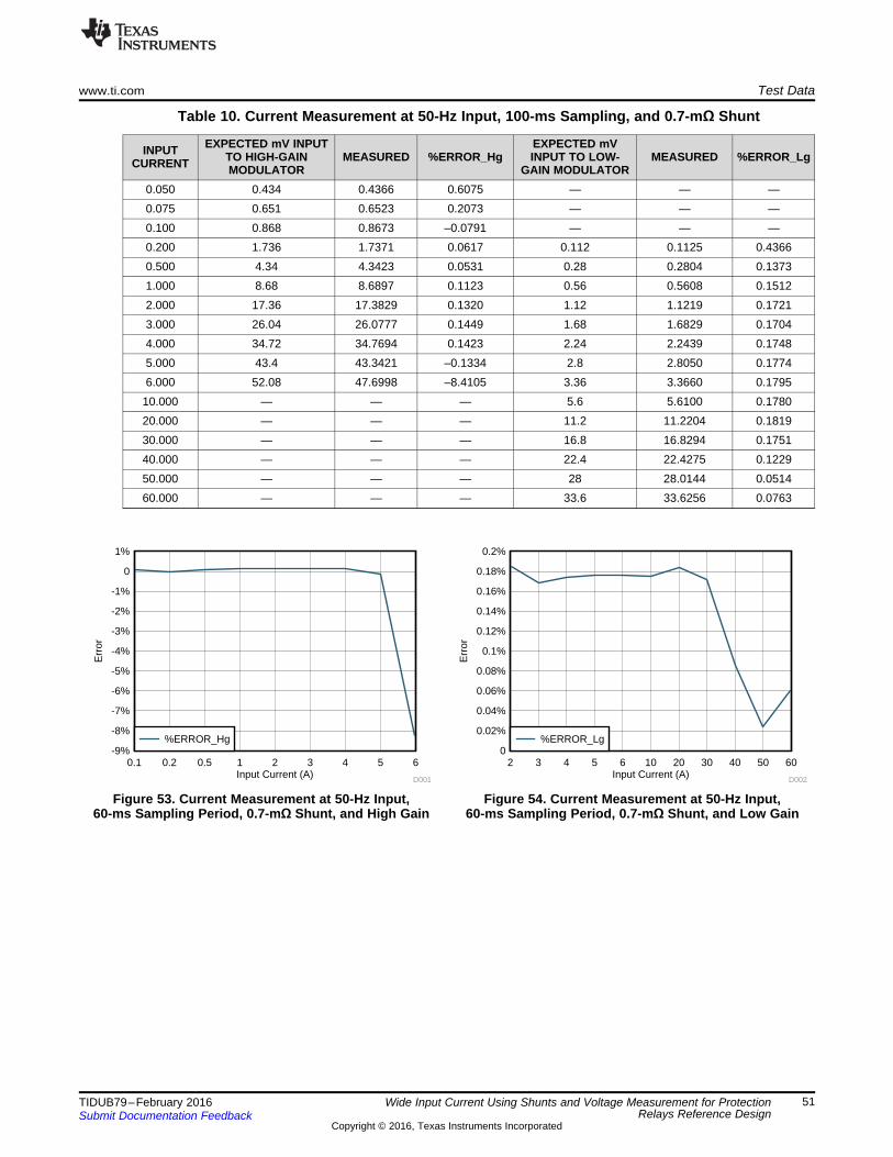
Input Current (A)
Err
or
-9%
-8%
-7%
-6%
-5%
-4%
-3%
-2%
-1%
0
1%
0.1 0.2 0.5 1 2 3 4 5 6
D001
%ERROR_Hg
Input Current (A)
Err
or
0
0.02%
0.04%
0.06%
0.08%
0.1%
0.12%
0.14%
0.16%
0.18%
0.2%
2 3 4 5 6 10 20 30 40 50 60
D002
%ERROR_Lg
www.ti.com Test Data
51TIDUB79–February 2016Submit Documentation Feedback
Copyright © 2016, Texas Instruments Incorporated
Wide Input Current Using Shunts and Voltage Measurement for ProtectionRelays Reference Design
Table 10. Current Measurement at 50-Hz Input, 100-ms Sampling, and 0.7-mΩ Shunt
INPUTCURRENT
EXPECTED mV INPUTTO HIGH-GAINMODULATOR
MEASURED %ERROR_HgEXPECTED mVINPUT TO LOW-
GAIN MODULATORMEASURED %ERROR_Lg
0.050 0.434 0.4366 0.6075 — — —0.075 0.651 0.6523 0.2073 — — —0.100 0.868 0.8673 –0.0791 — — —0.200 1.736 1.7371 0.0617 0.112 0.1125 0.43660.500 4.34 4.3423 0.0531 0.28 0.2804 0.13731.000 8.68 8.6897 0.1123 0.56 0.5608 0.15122.000 17.36 17.3829 0.1320 1.12 1.1219 0.17213.000 26.04 26.0777 0.1449 1.68 1.6829 0.17044.000 34.72 34.7694 0.1423 2.24 2.2439 0.17485.000 43.4 43.3421 –0.1334 2.8 2.8050 0.17746.000 52.08 47.6998 –8.4105 3.36 3.3660 0.1795
10.000 — — — 5.6 5.6100 0.178020.000 — — — 11.2 11.2204 0.181930.000 — — — 16.8 16.8294 0.175140.000 — — — 22.4 22.4275 0.122950.000 — — — 28 28.0144 0.051460.000 — — — 33.6 33.6256 0.0763
Figure 53. Current Measurement at 50-Hz Input,60-ms Sampling Period, 0.7-mΩ Shunt, and High Gain
Figure 54. Current Measurement at 50-Hz Input,60-ms Sampling Period, 0.7-mΩ Shunt, and Low Gain

Input Current (A)
Err
or
-8%
-7%
-6%
-5%
-4%
-3%
-2%
-1%
0
1%
0.05 0.075 0.1 0.2 0.5 1 2 3 4
D003
%ERROR_Hg
Input Current (A)
Err
or
-6%
-5%
-4%
-3%
-2%
-1%
0
1%
0.5 1 2 3 4 5 6 10 20 30 40 50 60
D004
%ERROR_Lg
Test Data www.ti.com
52 TIDUB79–February 2016Submit Documentation Feedback
Copyright © 2016, Texas Instruments Incorporated
Wide Input Current Using Shunts and Voltage Measurement for ProtectionRelays Reference Design
Board testing with a 1-mΩ shunt:
Table 11. Current Measurement at 50-Hz Input, 60-ms Sampling, and 1-mΩ Shunt
INPUTCURRENT
EXPECTED mV INPUTTO HIGH-GAINMODULATOR
MEASURED %ERROR_HgEXPECTED mVINPUT TO LOW-
GAIN MODULATORMEASURED %ERROR_Lg
0.050 0.62 0.6218 0.2978 — — —0.075 0.93 0.9312 0.1274 — — —0.100 1.24 1.2399 –0.0055 — — —0.200 2.48 2.4813 0.0540 — — —0.500 6.2 6.2005 0.0088 0.4 0.4003 0.07571.000 12.4 12.4035 0.0283 0.8 0.8007 0.08942.000 24.8 24.8100 0.0402 1.6 1.6016 0.09843.000 37.2 37.2139 0.0373 2.4 2.4024 0.10184.000 49.6 45.8367 –7.5873 3.2 3.2035 0.11015.000 — — — 4 4.0046 0.11606.000 — — — 4.8 4.8062 0.1302
10.000 — — — 8 8.0120 0.150620.000 — — — 16 16.0385 0.240730.000 — — — 24 24.0660 0.275140.000 — — — 32 32.1298 0.405650.000 — — — 40 40.2686 0.671560.000 — — — 48 45.6094 –4.9803
NOTE: The error at higher current varies as a result of self heating on the shunt.
Figure 55. Current Measurement at 50-Hz Input,60-ms Sampling Period, 1-mΩ Shunt, and High Gain
Figure 56. Current Measurement at 50-Hz Input,60-ms Sampling Period, 1-mΩ Shunt, and Low Gain

www.ti.com Test Data
53TIDUB79–February 2016Submit Documentation Feedback
Copyright © 2016, Texas Instruments Incorporated
Wide Input Current Using Shunts and Voltage Measurement for ProtectionRelays Reference Design
9.1.2 Current Measurement at 60 Hz
Table 12. Current Measurement at 60-Hz Input, 60-ms Sampling, and 0.7-mΩ Shunt
INPUTCURRENT
EXPECTED mV INPUTTO HIGH-GAINMODULATOR
MEASURED %ERROR_HgEXPECTED mVINPUT TO LOW-
GAIN MODULATORMEASURED %ERROR_Lg
0.050 0.434 0.4376 0.8273 — — —0.075 0.651 0.6527 0.2604 — — —0.10 0.868 0.8678 -0.0222 — — —0.20 1.736 1.7363 0.0169 0.112 0.1123 0.29640.50 4.34 4.3426 0.0590 0.28 0.2804 0.15261.00 8.68 8.6885 0.0976 0.56 0.5611 0.19702.00 17.36 17.3796 0.1128 1.12 1.1219 0.16683.00 26.04 26.0711 0.1196 1.68 1.6827 0.16334.00 34.72 34.7630 0.1238 2.24 2.2437 0.16465.00 43.4 43.3299 -0.1615 2.8 2.8045 0.15906.00 52.08 47.6932 -8.4232 3.36 3.3654 0.160010.00 — — — 5.6 5.6093 0.165220.00 — — — 11.2 11.2190 0.169530.00 — — — 16.8 16.8274 0.163240.00 — — — 22.4 22.4265 0.118450.00 — — — 28 28.0016 0.005660.00 — — — 33.6 33.6213 0.0633
Table 13. Current Measurement at 60-Hz Input, 100-ms Sampling, and 0.7-mΩ Shunt
INPUTCURRENT
EXPECTED mV INPUTTO HIGH-GAINMODULATOR
MEASURED %ERROR_HgEXPECTED mVINPUT TO LOW-
GAIN MODULATORMEASURED %ERROR_Lg
0.050 0.434 0.4363 0.5211 — — —0.075 0.651 0.6517 0.1132 — — —0.10 0.868 0.8675 –0.0544 — — —0.20 1.736 1.7354 –0.0364 0.112 0.1122 0.22090.50 4.34 4.3433 0.0767 0.28 0.2804 0.14801.00 8.68 8.6883 0.0959 0.56 0.5610 0.17122.00 17.36 17.3805 0.1179 1.12 1.1218 0.16503.00 26.04 26.0729 0.1264 1.68 1.6827 0.16094.00 34.72 34.7602 0.1159 2.24 2.2433 0.14595.00 43.4 43.3363 –0.1467 2.8 2.8045 0.16226.00 52.08 47.6945 –8.4207 3.36 3.3657 0.170410.00 — — — 5.6 5.6092 0.165020.00 — — — 11.2 11.2195 0.173930.00 — — — 16.8 16.8254 0.151440.00 — — — 22.4 22.4260 0.116250.00 — — — 28 28.0074 0.026660.00 — — — 33.6 33.5981 –0.0057

Input Current (A)
Err
or
-9%
-8%
-7%
-6%
-5%
-4%
-3%
-2%
-1%
0
1%
0.1 0.2 0.5 1 2 3 4 5 6
D005
%ERROR_Hg
Input Current (A)
Err
or
-0.02%
0
0.02%
0.04%
0.06%
0.08%
0.1%
0.12%
0.14%
0.16%
0.18%
0.2%
1 2 3 4 5 6 10 20 30 40 50 60
D006
%ERROR_Lg
Test Data www.ti.com
54 TIDUB79–February 2016Submit Documentation Feedback
Copyright © 2016, Texas Instruments Incorporated
Wide Input Current Using Shunts and Voltage Measurement for ProtectionRelays Reference Design
Figure 57. Current Measurement at 60-Hz Input,100-ms Sampling Period, 0.7-mΩ Shunt, and High Gain
Figure 58. Current Measurement at 60-Hz Input,100-ms Sampling Period, 0.7-mΩ Shunt, and Low Gain
9.1.3 DC Current Measurement
Table 14. DC Current Measurement—High-Gain Stage With 100-ms Samples and 0.7-mΩ Shunt
CURRENT INPUT NORMAL CURRENT INPUT REVERSED(NEGATIVE SIGN NOT SHOWN)
INPUT CURRENT GUI MEASUREMENT INPUT CURRENT GUI MEASUREMENT AVERAGEIDC (A) IDC (A) %ERROR IDC (A) IDC (A) %ERROR CURRENT %ERROR0.051 0.0503 –0.3201 0.051 0.0513 1.5460 0.0508 0.61300.075 0.0752 –0.3004 0.075 0.0764 1.1996 0.0758 0.44960.100 0.1005 0.0226 0.100 0.1012 0.7550 0.1008 0.38880.200 0.2009 0.2078 0.200 0.2013 0.4292 0.2011 0.31850.500 0.5016 0.2263 0.500 0.5020 0.3131 0.5018 0.26971.000 1.0026 0.2607 1.000 1.0034 0.3380 1.0030 0.29932.000 2.0067 0.3325 2.000 2.0058 0.2923 2.0062 0.31243.000 3.0081 0.2697 3.000 3.0090 0.2986 3.0085 0.2841

www.ti.com Test Data
55TIDUB79–February 2016Submit Documentation Feedback
Copyright © 2016, Texas Instruments Incorporated
Wide Input Current Using Shunts and Voltage Measurement for ProtectionRelays Reference Design
9.1.3.1 Repeatability Testing With AC Current Input and Power Cycling of AFE BoardThe repeatability testing was performed with a 2-A current using a modulator with a high-gain amplifierinput.
Procedure:• The board is powered up and a 2-A current is applied for 10 to 15 min.• After 15 min of accuracy, the AFE is tested and the measurements are noted.• The board DC input voltage is powered off for 5 min, including current input.• The measurement cycle is repeated.
Table 15. Repeatability Testing at 50-Hz High-Gain Stage With Samples Taken for 100 ms
BOARD STATUS APPLIED CURRENT INPUT GUI MEASUREMENT (A) % ERRORReading Number 1
Reading 2.0 2.0036 0.1827Reading Number 2
Reading 2.0 2.0034 0.1719Reading Number 3
Reading 2.0 2.003202 0.1600Reading Number 4
Reading 2.0 2.0033 0.1661Reading Number 5
Reading 2.0 2.0037 0.1890Reading Number 6
Reading 2.0 2.0035 0.1789
9.1.4 Repeatability Testing (Long-Term Stability) With AC Current InputA constant current was applied and measurements were repeated every 15 min.
Table 16. Repeatability Testing at 50-Hz Input, 100-ms Sampling
INPUTCURRENT
EXPECTED mV INPUTTO HIGH-GAINMODULATOR
MEASURED %ERROR_HgEXPECTED mVINPUT TO LOW-
GAIN MODULATORMEASURED %ERROR_Lg
3.0 26.0400 26.0754 0.1358 1.6800 1.6829 0.17043.0 26.0400 26.0765 0.1400 1.6800 1.6826 0.15563.0 26.0400 26.0771 0.1426 1.6800 1.6829 0.17333.0 26.0400 26.0765 0.1400 1.6800 1.6827 0.16213.0 26.0400 26.0759 0.1377 1.6800 1.6827 0.16273.0 26.0400 26.0772 0.1430 1.6800 1.6828 0.16743.0 26.0400 26.0765 0.1400 1.6800 1.6828 0.16683.0 26.0400 26.0775 0.1441 1.6800 1.6826 0.15623.0 26.0400 26.0771 0.1426 1.6800 1.6828 0.16623.0 26.0400 26.0782 0.1468 1.6800 1.6829 0.1698
NOTE: The variation is less than 0.1% for measurements that were taken for more than two hours.

Test Data www.ti.com
56 TIDUB79–February 2016Submit Documentation Feedback
Copyright © 2016, Texas Instruments Incorporated
Wide Input Current Using Shunts and Voltage Measurement for ProtectionRelays Reference Design
9.1.5 VA Burden for Current Input (Power Dissipation Across Shunt at Nominal Current In of 1 A)
Table 17. Shunt Input VA Measurement
PARAMETER VALUEExpected burden at 1-A In < 0.1 VAMeasured VA drop for 0.7 mΩ 0.0007 VA (0.7 mΩ × 1 A = 0.7 mVA)Measured VA drop for 1 mΩ 0.001 VA (1 mΩ × 1 A = 1 mVA)
9.2 Voltage MeasurementA ±250-mV input-rated modulator was used to measure the AC voltage input. The result was monitored onchannel 6 of the GUI. The voltage was applied across the onboard potential divider to enable a directconnection of voltage up to 300 V.
9.2.1 AC Voltage Measurement
Table 18. Voltage Measurement at 50-Hz Input and 60-ms Sampling
INPUT VOLTAGE EXPECTED mV INPUT TO MODULATOR MEASURED %ERROR1.000 0.615 0.6142 –0.13322.500 1.5375 1.5360 –0.09955.000 3.075 3.0717 –0.1067
10.000 6.15 6.1456 –0.072325.000 15.375 15.3627 –0.079850.000 30.75 30.7311 –0.0615100.000 61.5 61.4766 –0.0381150.000 92.25 92.2343 –0.0170200.000 123 123.0046 0.0038250.000 153.75 153.7943 0.0288300.000 184.5 184.5990 0.0537325.000 199.875 199.9858 0.0554350.000 215.25 215.3957 0.0677
Table 19. Voltage Measurement at 60-Hz Input and 60-ms Sampling
INPUT VOLTAGE EXPECTED mV INPUT TO MODULATOR MEASURED %ERROR1.000 0.615 0.6143 –0.11092.500 1.5375 1.5364 –0.07465.000 3.075 3.0711 –0.127910.000 6.15 6.1442 –0.094425.000 15.375 15.3624 –0.081850.000 30.75 30.7238 –0.0851100.000 61.5 61.4573 –0.0694150.000 92.25 92.2171 –0.0357200.000 123 122.9825 –0.0142250.000 153.75 153.7731 0.0150300.000 184.5 184.5688 0.0373325.000 199.875 199.9616 0.0433350.000 215.25 215.3766 0.0588

Input Voltage (V)
Err
or
-0.15%
-0.1%
-0.05%
0
0.05%
0.1%
1 2.5 5 10 25 50 100 150 200 250 300 325 350
D007
%ERROR
Input Voltage (V)
Err
or
-0.15%
-0.1%
-0.05%
0
0.05%
0.1%
1 2.5 5 10 25 50 100 150 200 250 300 325 350
D008
%ERROR
www.ti.com Test Data
57TIDUB79–February 2016Submit Documentation Feedback
Copyright © 2016, Texas Instruments Incorporated
Wide Input Current Using Shunts and Voltage Measurement for ProtectionRelays Reference Design
Figure 59. Voltage Measurement at 50-Hz Inputand 60-ms Sampling
Figure 60. Voltage Measurement at 60-Hz Inputand 60-ms Sampling
Accuracy testing for second board:
Table 20. Voltage Measurement at 50-Hz Input and 60-ms Sampling
INPUT VOLTAGE EXPECTED INPUT mV TO MODULATOR MEASURED %ERROR1.000 0.615 0.613629 –0.222952.500 1.5375 1.536675 –0.053655.000 3.075 3.073672 –0.0431910.000 6.15 6.147233 –0.0449925.000 15.375 15.36675 –0.0536550.000 30.75 30.73672 –0.04319100.000 61.5 61.48429 –0.02554150.000 92.25 92.25619 0.006706200.000 123 123.0411 0.033451250.000 153.75 153.8474 0.063356300.000 184.5 184.6708 0.092553325.000 199.875 200.0875 0.106296350.000 215.25 215.5102 0.120878

Test Data www.ti.com
58 TIDUB79–February 2016Submit Documentation Feedback
Copyright © 2016, Texas Instruments Incorporated
Wide Input Current Using Shunts and Voltage Measurement for ProtectionRelays Reference Design
9.2.2 DC Voltage MeasurementThe TIDA-00738 TI Design can be used for DC measurement. Table 21 shows the test results for DCvoltage measurement.
Table 21. DC Voltage Measurement at 60 ms
VOLTAGE INPUT (+ THEN –) VOLTAGE INPUT (– THEN +)VIN GUI MEASUREMENT VIN GUI MEASUREMENT
V-DC (V) V-DC (V) %ERROR V-DC (V) V-DC (V) %ERROR10.075 10.07 0.027 –10.045 –10.08 –0.35820.055 20.06 –0.032 –20 –20.05 –0.25130.054 30.08 –0.086 –30.075 –30.14 –0.20240.035 40.07 –0.092 –40.039 –40.12 –0.196100.071 100.21 –0.136 –100.045 –100.22 –0.179110.085 110.24 –0.144 –110.093 –110.29 –0.181120.025 120.20 –0.147 –120.05 –120.27 –0.185130.045 130.24 –0.148 –130.04 –130.28 –0.184220.06 220.47 –0.186 –220 –220.47 –0.212240.09 240.56 –0.195 –240 –240.52 –0.216
280 280.62 –0.220 –280.09 –280.73 –0.230300.09 300.75 –0.219 –300.06 –300.77 –0.236
9.3 Summary of Test Results
Table 22. Test Results Summary
SERIALNUMBER
MEASUREMENTPARAMETER
VALUE FREQUENCY(Hz)
SAMPLINGTIME RESULT
MIN MAX
1 Current AC (A)0.1 5 50 or 60 3 or 5 cycles <± 0.5%1 40 (or 60) 50 or 60 3 or 3 cycles <± 0.5%
2 Voltage AC (V)10 300 50 5 cycles <± 0.5%10 300 60 5 cycles <± 0.5%
3 Repeatability testing withpower cycling AC current (A) 2 50 5 cycles <± 0.5%
4
Power supply testing
Isolated power for currentmeasurement
+5 V isolated N/A N/A OK±2.5 V Isolated N/A N/A OK
Isolated power for voltagemeasurement
+5 V isolated N/A N/A OK±2.5 V Isolated N/A N/A OK
5 DC current measurement OK6 DC voltage measurement OK
www.ti.com Design Files
59TIDUB79–February 2016Submit Documentation Feedback
Copyright © 2016, Texas Instruments Incorporated
Wide Input Current Using Shunts and Voltage Measurement for ProtectionRelays Reference Design
10 Design Files
10.1 SchematicsTo download the schematics for each board, see the design files at TIDA-00738.
10.2 Bill of MaterialsTo download the Bill of Materials (BOM), see the design files at TIDA-00738.
10.3 Layout PrintsTo download the layout prints for each board, see the design files at TIDA-00738.
10.4 Altium ProjectTo download the Altium project files for each board, see the design files at TIDA-00738.
10.5 Gerber FilesTo download the Gerber files for each board, see the design files at TIDA-00738.
10.6 Assembly DrawingsTo download the assembly drawings for each board, see the design files at TIDA-00738.
11 References
1. Texas Instruments, Isolated Current (Shunt-Based) and Voltage Sensing for Smart Grid Applications,TIDA-00080 Design Guide (TIDU429)
2. Texas Instruments, Isolated Current Shunt and Voltage Measurement Kit,TIDA-00171 Design Guide (TIDU499)
3. Texas Instruments, AM437x SYSBIOS Industrial SDK 02.00.00.02 User Guide, Wiki(http://processors.wiki.ti.com/index.php/AM437x_SYSBIOS_Industrial_SDK_02.00.00.02_User_Guide)
4. Texas Instruments, Isolated Current Shunt and Voltage Measurement for Motor Drives Using AM437x,TIDA-00209 Design Guide (TIDU755)
12 TerminologyAFE— Analog front end
CT— Current transformer
IDK— Industrial development kit
IED— Intelligent electronic device
PD— Potential divider
PRU-ICSS— Programmable Real-Time Unit Subsystem
In— Nominal current
LVCMOS— Low-voltage complementary metal-oxide semiconductor

About the Author www.ti.com
60 TIDUB79–February 2016Submit Documentation Feedback
Copyright © 2016, Texas Instruments Incorporated
Wide Input Current Using Shunts and Voltage Measurement for ProtectionRelays Reference Design
13 About the AuthorAMIT KUMBASI is a systems architect at Texas Instruments Dallas where he is responsible fordeveloping subsystem solutions for Grid Infrastructure within Industrial Systems. Amit brings to this rolehis expertise with defining products, business development, and board level design using precision analogand mixed-signal devices. He holds a Master’s in ECE (Texas Tech) and an MBA (University of Arizona).He can be reached at [email protected].
KALLIKUPPA MUNIYAPPA SREENIVASA is a systems architect at Texas Instruments where he isresponsible for developing reference design solutions for the industrial segment. Sreenivasa brings to thisrole his experience in high-speed digital and analog systems design. Sreenivasa earned his Bachelor ofElectronics (BE) in electronics and communication engineering (BE-E&C) from VTU, Mysore, India.
IMPORTANT NOTICE FOR TI REFERENCE DESIGNS
Texas Instruments Incorporated ("TI") reference designs are solely intended to assist designers (“Buyers”) who are developing systems thatincorporate TI semiconductor products (also referred to herein as “components”). Buyer understands and agrees that Buyer remainsresponsible for using its independent analysis, evaluation and judgment in designing Buyer’s systems and products.TI reference designs have been created using standard laboratory conditions and engineering practices. TI has not conducted anytesting other than that specifically described in the published documentation for a particular reference design. TI may makecorrections, enhancements, improvements and other changes to its reference designs.Buyers are authorized to use TI reference designs with the TI component(s) identified in each particular reference design and to modify thereference design in the development of their end products. HOWEVER, NO OTHER LICENSE, EXPRESS OR IMPLIED, BY ESTOPPELOR OTHERWISE TO ANY OTHER TI INTELLECTUAL PROPERTY RIGHT, AND NO LICENSE TO ANY THIRD PARTY TECHNOLOGYOR INTELLECTUAL PROPERTY RIGHT, IS GRANTED HEREIN, including but not limited to any patent right, copyright, mask work right,or other intellectual property right relating to any combination, machine, or process in which TI components or services are used.Information published by TI regarding third-party products or services does not constitute a license to use such products or services, or awarranty or endorsement thereof. Use of such information may require a license from a third party under the patents or other intellectualproperty of the third party, or a license from TI under the patents or other intellectual property of TI.TI REFERENCE DESIGNS ARE PROVIDED "AS IS". TI MAKES NO WARRANTIES OR REPRESENTATIONS WITH REGARD TO THEREFERENCE DESIGNS OR USE OF THE REFERENCE DESIGNS, EXPRESS, IMPLIED OR STATUTORY, INCLUDING ACCURACY ORCOMPLETENESS. TI DISCLAIMS ANY WARRANTY OF TITLE AND ANY IMPLIED WARRANTIES OF MERCHANTABILITY, FITNESSFOR A PARTICULAR PURPOSE, QUIET ENJOYMENT, QUIET POSSESSION, AND NON-INFRINGEMENT OF ANY THIRD PARTYINTELLECTUAL PROPERTY RIGHTS WITH REGARD TO TI REFERENCE DESIGNS OR USE THEREOF. TI SHALL NOT BE LIABLEFOR AND SHALL NOT DEFEND OR INDEMNIFY BUYERS AGAINST ANY THIRD PARTY INFRINGEMENT CLAIM THAT RELATES TOOR IS BASED ON A COMBINATION OF COMPONENTS PROVIDED IN A TI REFERENCE DESIGN. IN NO EVENT SHALL TI BELIABLE FOR ANY ACTUAL, SPECIAL, INCIDENTAL, CONSEQUENTIAL OR INDIRECT DAMAGES, HOWEVER CAUSED, ON ANYTHEORY OF LIABILITY AND WHETHER OR NOT TI HAS BEEN ADVISED OF THE POSSIBILITY OF SUCH DAMAGES, ARISING INANY WAY OUT OF TI REFERENCE DESIGNS OR BUYER’S USE OF TI REFERENCE DESIGNS.TI reserves the right to make corrections, enhancements, improvements and other changes to its semiconductor products and services perJESD46, latest issue, and to discontinue any product or service per JESD48, latest issue. Buyers should obtain the latest relevantinformation before placing orders and should verify that such information is current and complete. All semiconductor products are soldsubject to TI’s terms and conditions of sale supplied at the time of order acknowledgment.TI warrants performance of its components to the specifications applicable at the time of sale, in accordance with the warranty in TI’s termsand conditions of sale of semiconductor products. Testing and other quality control techniques for TI components are used to the extent TIdeems necessary to support this warranty. Except where mandated by applicable law, testing of all parameters of each component is notnecessarily performed.TI assumes no liability for applications assistance or the design of Buyers’ products. Buyers are responsible for their products andapplications using TI components. To minimize the risks associated with Buyers’ products and applications, Buyers should provideadequate design and operating safeguards.Reproduction of significant portions of TI information in TI data books, data sheets or reference designs is permissible only if reproduction iswithout alteration and is accompanied by all associated warranties, conditions, limitations, and notices. TI is not responsible or liable forsuch altered documentation. Information of third parties may be subject to additional restrictions.Buyer acknowledges and agrees that it is solely responsible for compliance with all legal, regulatory and safety-related requirementsconcerning its products, and any use of TI components in its applications, notwithstanding any applications-related information or supportthat may be provided by TI. Buyer represents and agrees that it has all the necessary expertise to create and implement safeguards thatanticipate dangerous failures, monitor failures and their consequences, lessen the likelihood of dangerous failures and take appropriateremedial actions. Buyer will fully indemnify TI and its representatives against any damages arising out of the use of any TI components inBuyer’s safety-critical applications.In some cases, TI components may be promoted specifically to facilitate safety-related applications. With such components, TI’s goal is tohelp enable customers to design and create their own end-product solutions that meet applicable functional safety standards andrequirements. Nonetheless, such components are subject to these terms.No TI components are authorized for use in FDA Class III (or similar life-critical medical equipment) unless authorized officers of the partieshave executed an agreement specifically governing such use.Only those TI components that TI has specifically designated as military grade or “enhanced plastic” are designed and intended for use inmilitary/aerospace applications or environments. Buyer acknowledges and agrees that any military or aerospace use of TI components thathave not been so designated is solely at Buyer's risk, and Buyer is solely responsible for compliance with all legal and regulatoryrequirements in connection with such use.TI has specifically designated certain components as meeting ISO/TS16949 requirements, mainly for automotive use. In any case of use ofnon-designated products, TI will not be responsible for any failure to meet ISO/TS16949.IMPORTANT NOTICE
Mailing Address: Texas Instruments, Post Office Box 655303, Dallas, Texas 75265Copyright © 2016, Texas Instruments Incorporated