wieman: 1 lbnl status and r&d plans for the star microvertex detector development 22-nov-03 lbnl...
TRANSCRIPT

Wieman: 1LBNL
Status and R&D plans for the STAR Microvertex Detector Development
22-Nov-03
LBNLFred Bieser, Robin Gareus (Heidelberg), Leo Greiner, Howard Matis, Marcus Oldenburg, Fabrice Retiere, Kai Schweda, Hans-Georg Ritter, Eugene Yamamoto, Howard Wieman
LEPSI/IReSClaude Colledani, Michel Pellicioli, Christian Olivetto, Christine Hu, Grzegorz Deptuch
Jerome Baudot, Fouad Rami, Wojciech, Dulinski, Marc Winter
UCIYandong Chen, Stuart Kleinfelder
BNL Instrumentation DivConsulting
OSUIvan Kotov
PurdueDennis Reichhold

Wieman: 2LBNL
Introduction
• Star Micro-Vertex detector– A high resolution inner vertex detector to measure D mesons in
Au+Au collisions
• Micro-Vertex detector development– Goals and Strategy
• Funded project 2006 (preliminary proposal this Dec)
• 1ST Generation based on LEPSI/IReS MIMOSA-5 CHIP (slow read out)
• 2nd Generation fast readout – to be determined
– Activities
• Simulations
• MIMOSA-5 readout
• Advanced APS development
• Mechanical

Wieman: 3LBNL
Features
• 2 layers
• Inner radius ~1.8 cm
• Active length 20 cm
• Readout speed 20 ms (generation 1)
• Number of pixels 130 M

Wieman: 4LBNL
Simulations
• Original work of Retiere and Matis show substantial improvement in D meson statistics, simulations based on parameterized performance of STAR detectors
• Full tracking detailed simulations (Schweda and Retiere) awaiting tracking debug– Cut optimization
– Refinement of detector requirements (pixel size)

Wieman: 5LBNL
MIMOSA-5 LEPSI/IReS chip readout (first generation progress)
• MIMOSA-5, full wafer engineering run – significant readout infrastructure on chip
• LBNL test board works (Bieser and Gareus) – 2 by 2 cm MIMOSA-5 chip
– LBNL development using 4 commercial 50 MHz 14 bit ADCs
• Considering piggy back readout chip design with CDS and signal scarification– Full frame by frame
comparison for CDS, i.e. memory for frame storage and leakage current subtraction

Wieman: 6LBNL
APS mile stones (first generation)
• Choose MIMOSTAR fabrication process, End 03• Thinned MIMOSA-5 chips to LEPSI/IReS, Feb. 04• Design of LEPSI/IReS MIMOSTAR chip, May 04• Tested MIMOSA-5 to LBNL, June 04• Submit fabrication MIMOSTAR, 2 proto, Sept 04• First ladder prototype, start Oct. 04• Tests of 2 MIMOSTAR prototypes, Jan 05• Final MIMOSTAR prototype design, Mar 05• Submit fab final MIMOSTAR prototype, Apr 05• Production tests of final MIMOSTAR proto type on wafer,
July 05• Send MIMOSTAR for thinning, Aug 05• Test thinned and diced MIMOSTAR prototype chips, Sept 05• Mount MIMOSTAR chips on final ladder prototype

Wieman: 7LBNL
Read out chip, mile stones
• Requirements specification, Feb. 04
• Submit fab prototype, Oct. 04
• Tested prototype, Feb 05
• Submit fab final, May 05

Wieman: 8LBNL
Advanced APS designs
• Goal, increase speed with on detector chip zero suppress and by avoiding full frame readout
• Requires improvements in signal to noise– Noise sources
• KTC reset noise
• Fixed pattern noise, threshold variation, leakage current variation
• Programs at LEPSI/IReS
• Programs at UCI/LBNL (Stuart Kleinfelder, Yandong Chen)– Photogates
– CDS clamp circuit
– Active Reset

Wieman: 9LBNL
• CDS removal of fixed pattern noise and KTC reset noise on the chip (standard diode requires CDS off chip)
• Increase signal by reducing signal spreading to adjacent pixels. The photo gate permits large geometry without adding capacitance to the sense node.
Photo gate purpose - addresses standard diode limitations
P-
P
P+
Standard diode geometry
Standard APS diode structure

Wieman: 10LBNL
photo gate
source follower gate
reset gate
transfer gate
row select gate
sense node drain
• Large photo-gate to collect large fraction of the charge on a single pixel, directly on the p- epi layer
• Small transfer gate also directly on p- epi layer
• Small drain (minimum capacitance) connected to source follower gate (sense node)
Photo-gate geometry
20 m
x -2 m- 1 m 1 m5 nm
8 m
0.1 m
0.4 m
P epi 1.4x10¹⁵ 1/cm3
N+ 1x10²⁰ 1/cm3
photo gate transfer gate
drain
x = 0.4 and 0.8 m
(simulation quantities)

Wieman: 11LBNL
First silicon tests, comparing photo-gate with standard diode structure
Photo-gate directly to sense node drain
DC bias:V photo-gate 0.6 VV drain 2.4 V
Output signal for Fe55 X-ray test
Issue:
ADC
Linear
ADC
Log
diode
Photo-gate 1
Photo-gate 2
diode - fullcharge collection
Why is the signal spread out – is it surface traps under the gate?

Wieman: 12LBNL
CDS clamp
• kTC noise removed by clamp circuit – noise scales as
2CkT
Rather than
diodekTC

Wieman: 13LBNL
Active reset
• Signal from output is amplified to zero the input
• In test
Our standard APS gives10 electrons RMS after CDS

Wieman: 14LBNL
Mechanical
• Rapid insertion and removal for replacement and changing detector configuration
• Minimum thickness: 50 Micron Si Detector – 50 Micron Si Readout chip
• Air cooling
• Composite beam pipe?

Wieman: 15LBNL
Thin stiff ladder concept
• Under development
• Will be tested for vibration in our wind tunnel
carbon composite (75 m)Young’s modulus 3-4 times steel
aluminum kapton cable(100 m)
silicon chips(50 m)
21.6 mm
254 mm

Wieman: 16LBNL

Wieman: 17LBNL
Air cooling and vibration
• 1-2 m/s air cools 100 mW/cm2
• TV holography shows 2 m vibration for tensioned silicon structure
TV holography vibration map
Lucite wind tunnel Thin silicon ladder,tension support
Laser light source
Camera

Wieman: 18LBNL
Inner STAR model – SVT and micro-vertex
Wieman: 19LBNL
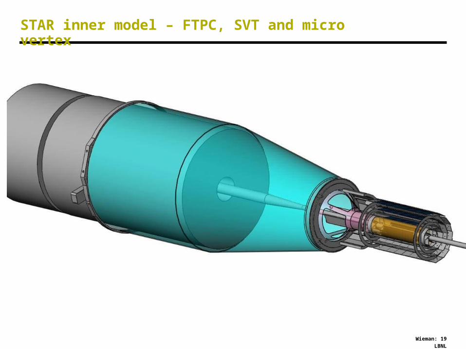
STAR inner model – FTPC, SVT and micro vertex

Wieman: 20LBNL
The reality

Wieman: 21LBNL
Summary
• First generation: LEPSI/IReS MIMOSA-5– R&D $s required for foundry costs
• Piggy back readout chip– R&D $s required for foundry costs and student
• Advanced APS design in progress– R&D $s required for foundry costs and student
• Micro-vertex detector is being designed to go inside SVT
• It is being designed for rapid insertion and removal– R&D $s for Engineer/Tech prototypes and test fixtures
• Thin beam pipe– R&D $s for Engineer/Tech prototypes and test fixtures
FY04 $360kFY05 $495k