winbond w2e512/w27e257 eeprom - the chip …smithsonianchips.si.edu/ice/cd/9703_533.pdf · - 1 -...
TRANSCRIPT

Construction Analysis
Winbond W2E512/W27E257EEPROM
Report Number: SCA 9703-533
®
Serv
ing
the
Global Semiconductor Industry
Since1964
15022 N. 75th StreetScottsdale, AZ 85260-2476
Phone: 602-998-9780Fax: 602-948-1925
e-mail: [email protected]: http://www.ice-corp.com/ice
- i -
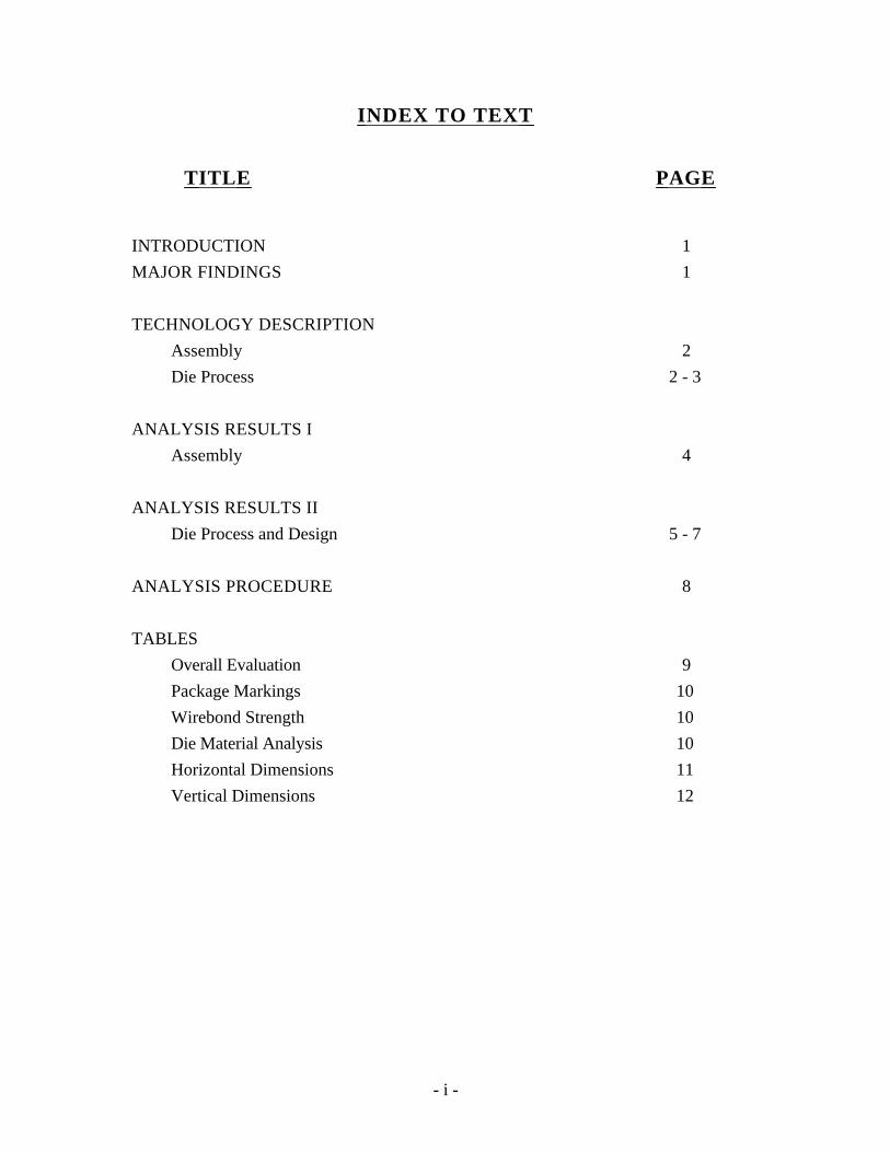
INDEX TO TEXT
TITLE PAGE
INTRODUCTION 1
MAJOR FINDINGS 1
TECHNOLOGY DESCRIPTION
Assembly 2
Die Process 2 - 3
ANALYSIS RESULTS I
Assembly 4
ANALYSIS RESULTS II
Die Process and Design 5 - 7
ANALYSIS PROCEDURE 8
TABLES
Overall Evaluation 9
Package Markings 10
Wirebond Strength 10
Die Material Analysis 10
Horizontal Dimensions 11
Vertical Dimensions 12

- 1 -
INTRODUCTION
This report describes a competitive analysis of the WINBOND 512K and 256K
EEPROM. Two devices of each type were received for the analysis. Since the processes
used were almost identical, only minimal analysis of the 256K device is included, and in all
cases identified as such. The devices were packaged in 28-pin Dual In-line Packages
(DIPs). Possible date codes were 9647 for the 512K, and 9627 for the 256K devices.
MAJOR FINDINGS
Questionable Items:1
• Aluminum thinning up to 90 percent2 (Figure 21). Barrier metal maintained continuity.
With the addition of a cap and barrier metal, overall metal thinning was 85 percent.
Special Features:
• Unique (WINBOND) cell design.
1These items present possible quality or reliability concerns. They should be discussedwith the manufacturer to determine their possible impact on the intended application.
2Seriousness depends on design margins.
- 2 -
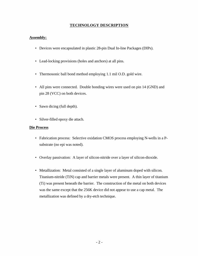
TECHNOLOGY DESCRIPTION
Assembly:
• Devices were encapsulated in plastic 28-pin Dual In-line Packages (DIPs).
• Lead-locking provisions (holes and anchors) at all pins.
• Thermosonic ball bond method employing 1.1 mil O.D. gold wire.
• All pins were connected. Double bonding wires were used on pin 14 (GND) and
pin 28 (VCC) on both devices.
• Sawn dicing (full depth).
• Silver-filled epoxy die attach.
Die Process
• Fabrication process: Selective oxidation CMOS process employing N-wells in a P-
substrate (no epi was noted).
• Overlay passivation: A layer of silicon-nitride over a layer of silicon-dioxide.
• Metallization: Metal consisted of a single layer of aluminum doped with silicon.
Titanium-nitride (TiN) cap and barrier metals were present. A thin layer of titanium
(Ti) was present beneath the barrier. The construction of the metal on both devices
was the same except that the 256K device did not appear to use a cap metal. The
metallization was defined by a dry-etch technique.

- 3 -
TECHNOLOGY DESCRIPTION (continued)
• Pre-metal dielectric: A layer of borophosphosilicate glass (BPSG) over various
densified oxides. This layer appeared to have been reflowed following contact cuts
on the 256K device and before contact cuts on the 512K device.
• Polysilicon: Two layers of dry-etched polysilicon (no silicide). Poly 2 was used to
form word lines in the array and all gates in the periphery. Poly 1 was used
exclusively to form floating gates in the cell array.
• Isolation: Local oxide (LOCOS).
• Diffusions: Standard implanted N+ and P+ diffusions were used for source and
drains. Oxide sidewall spacers were present on the gates indicating an LDD process
may have been used.
• Wells: N-wells in a P substrate. No step was noted in the oxide at the well
boundary. No epi was visible.
• Memory cells: The memory cell design consisted of poly 2 word lines and select
gates, and poly 1 floating gates. Metal formed the bit lines. Programming is
achieved by injecting electrons to and from the floating gate through Fowler-
Nordheim tunneling. Cell pitch was 2.6 x 3 microns.

- 4 -
ANALYSIS RESULTS I
Assembly: Figures 1 - 7
Questionable Items:1 None.
General Items:
• Devices were packaged in plastic 28-pin Dual In-line Packages (DIPs).
• Overall package quality: Normal. No defects were found on the external or internal
portions of the packages.
• Lead-locking provisions (anchors and holes) were present.
• Wirebonding: Thermosonic ball bond method using 1.1 mil O.D. gold wire. No
bond lifts occurred and bond pull strengths were good (see page 10). Wire spacing
and placement was normal. Double bonding wires were used for pins 14 and 28 on
both devices. All pins were connected.
• Die attach: Silver-filled epoxy of normal quantity and quality.
• Die dicing: Die separation was by sawing (full depth) with normal quality
workmanship.
1These items present possible quality or reliability concerns. They should be discussedwith the manufacturer to determine their possible impact on the intended application.

- 5 -
ANALYSIS RESULTS II
Die Process and Design: Figures 8 - 41
Questionable Items:1
• Aluminum thinning up to 90 percent2 (Figure 21). Barrier metal maintained continuity.
With the addition of a cap and barrier metal, overall metal thinning was 85 percent.
Special Features:
• Unique (WINBOND) cell design, ultra-thin tunnel oxide used for programming.
General Items:
• Fabrication process: Selective oxidation CMOS process employing N-wells in a P-
substrate (no epi).
• Design and layout: Die layout was clean and efficient. Alignment was good at all
levels.
• Die surface defects: None. No contamination, toolmarks or processing defects
were noted.
• Overlay passivation: A layer of silicon-nitride over a layer of silicon-dioxide.
Overlay integrity tests indicated defect-free passivation. Edge seal was good.
1These items present possible quality or reliability concerns. They should be discussed with the manufacturer to determine their possible impact on the intended application.
2Seriousness depends on design margins.
- 6 -
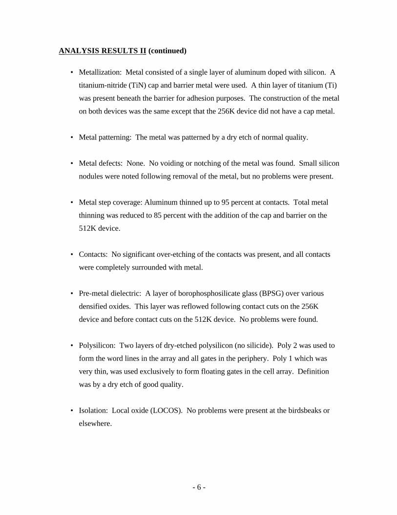
ANALYSIS RESULTS II (continued)
• Metallization: Metal consisted of a single layer of aluminum doped with silicon. A
titanium-nitride (TiN) cap and barrier metal were used. A thin layer of titanium (Ti)
was present beneath the barrier for adhesion purposes. The construction of the metal
on both devices was the same except that the 256K device did not have a cap metal.
• Metal patterning: The metal was patterned by a dry etch of normal quality.
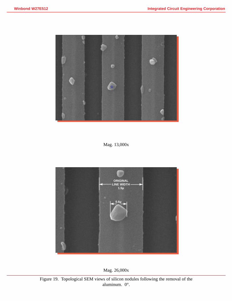
• Metal defects: None. No voiding or notching of the metal was found. Small silicon
nodules were noted following removal of the metal, but no problems were present.
• Metal step coverage: Aluminum thinned up to 95 percent at contacts. Total metal
thinning was reduced to 85 percent with the addition of the cap and barrier on the
512K device.
• Contacts: No significant over-etching of the contacts was present, and all contacts
were completely surrounded with metal.
• Pre-metal dielectric: A layer of borophosphosilicate glass (BPSG) over various
densified oxides. This layer was reflowed following contact cuts on the 256K
device and before contact cuts on the 512K device. No problems were found.
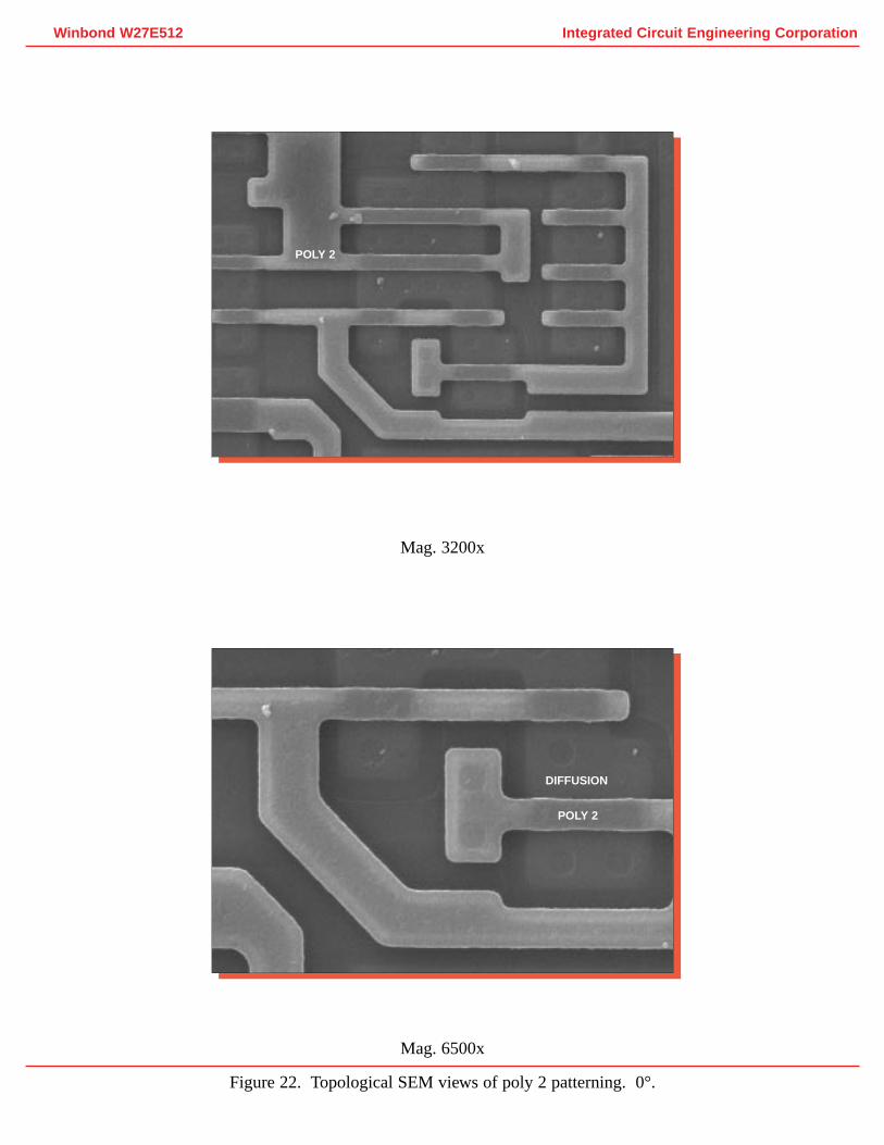
• Polysilicon: Two layers of dry-etched polysilicon (no silicide). Poly 2 was used to
form the word lines in the array and all gates in the periphery. Poly 1 which was
very thin, was used exclusively to form floating gates in the cell array. Definition
was by a dry etch of good quality.
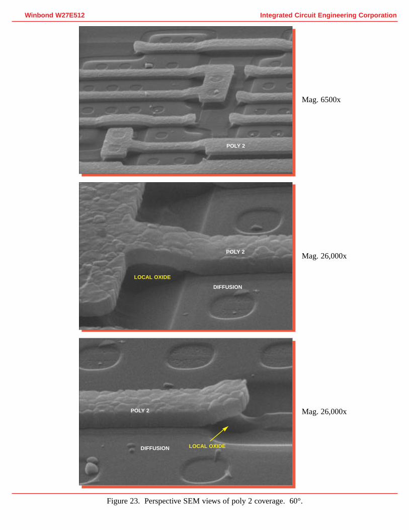
• Isolation: Local oxide (LOCOS). No problems were present at the birdsbeaks or
elsewhere.
- 7 -
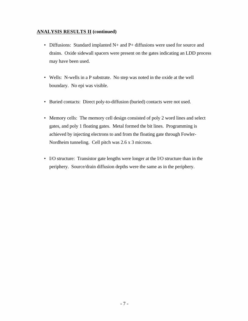
ANALYSIS RESULTS II (continued)
• Diffusions: Standard implanted N+ and P+ diffusions were used for source and
drains. Oxide sidewall spacers were present on the gates indicating an LDD process
may have been used.
• Wells: N-wells in a P substrate. No step was noted in the oxide at the well
boundary. No epi was visible.
• Buried contacts: Direct poly-to-diffusion (buried) contacts were not used.
• Memory cells: The memory cell design consisted of poly 2 word lines and select
gates, and poly 1 floating gates. Metal formed the bit lines. Programming is
achieved by injecting electrons to and from the floating gate through Fowler-
Nordheim tunneling. Cell pitch was 2.6 x 3 microns.
• I/O structure: Transistor gate lengths were longer at the I/O structure than in the
periphery. Source/drain diffusion depths were the same as in the periphery.

- 8 -
PROCEDURE
The devices were subjected to the following analysis procedures:
External inspection
X-ray
Decapsulation
Internal optical inspection
SEM inspection of assembly features and passivation
Passivation integrity tests
Wirepull tests
Passivation removal
SEM inspection of metal
Metal removal and inspect for silicon nodules
Delayer to poly and inspect poly structures and die surface
Die sectioning (90° for SEM)*
Measure horizontal dimensions
Measure vertical dimensions
Die material analysis
*Delineation of cross-sections is by silicon etch unless otherwise indicated.

- 9 -
OVERALL QUALITY EVALUATION: Overall Rating: Normal
DETAIL OF EVALUATION
Package integrity G
Package markings G
Die placement G
Die attach quality G
Wire spacing G
Wirebond placement G
Wirebond quality G
Dicing quality G
Wirebond method Thermosonic ball bonds using 1.1
mil gold wire.
Die attach method Silver-filled epoxy
Dicing method: Sawn (full depth)
Die surface integrity:
Tool marks (absence) G
Particles (absence) G
Contamination (absence) G
Process defects (absence) G
General workmanship N
Passivation integrity G
Metal definition G
Metal integrity1 NP
Contact coverage G
Contact registration G
Contact defects N
190 percent aluminum thinning on the 512K device.
G = Good, P = Poor, N = Normal, NP = Normal/Poor

- 10 -
PACKAGE MARKINGS 512K
Top Bottom
(LOGO) Winbond TAIWAN PA1
W27E512-12 QC26387460
647QC263874601PA
PACKAGE MARKINGS 256K
(LOGO) Winbond TAIWAN 0B2W27E257-12 AJ16207400627AJ16207400208B
WIREBOND STRENGTH
Wire material: 1.1 mil diameter gold
Die pad material: aluminum
Material at package post: silver
Sample # 512K 256K
# of wires tested: 14 9
Bond lifts: 0 0
Force to break - high: 8.5g 11g
- low: 6g 7g
- avg.: 7.2g 8.8g
- std. dev.: 1.9 1.7
DIE MATERIAL ANALYSIS
Passivation: Silicon-nitride over silicon-dioxide.
Metallization: Silicon-doped aluminum with a titanium-nitride cap and barrier.*
*There is no known method for accurately determining the amount of silicon in the aluminum on afinished die.
- 11 -
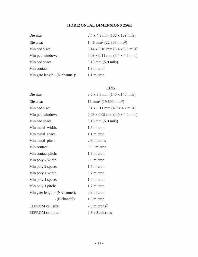
HORIZONTAL DIMENSIONS 256K
Die size: 3.4 x 4.3 mm (132 x 169 mils)
Die area: 14.6 mm2 (22,308 mils2)
Min pad size: 0.14 x 0.16 mm (5.4 x 6.6 mils)
Min pad window: 0.09 x 0.11 mm (3.4 x 4.5 mils)
Min pad space: 0.15 mm (5.9 mils)
Min contact: 1.3 micron
Min gate length - (N-channel): 1.1 micron
512K
Die size: 3.6 x 3.6 mm (140 x 140 mils)
Die area: 13 mm2 (19,600 mils2)
Min pad size: 0.1 x 0.11 mm (4.0 x 4.2 mils)
Min pad window: 0.09 x 0.09 mm (4.0 x 4.0 mils)
Min pad space: 0.13 mm (5.3 mils)
Min metal width: 1.5 micron
Min metal space: 1.1 micron
Min metal pitch: 2.6 microns
Min contact: 0.95 micron
Min contact pitch: 1.9 micron
Min poly 2 width: 0.9 micron
Min poly 2 space: 1.5 micron
Min poly 1 width: 0.7 micron
Min poly 1 space: 1.0 micron
Min poly 1 pitch: 1.7 micron
Min gate length - (N-channel): 0.9 micron
- (P-channel): 1.0 micron
EEPROM cell size: 7.8 microns2
EEPROM cell pitch: 2.6 x 3 microns
- 12 -
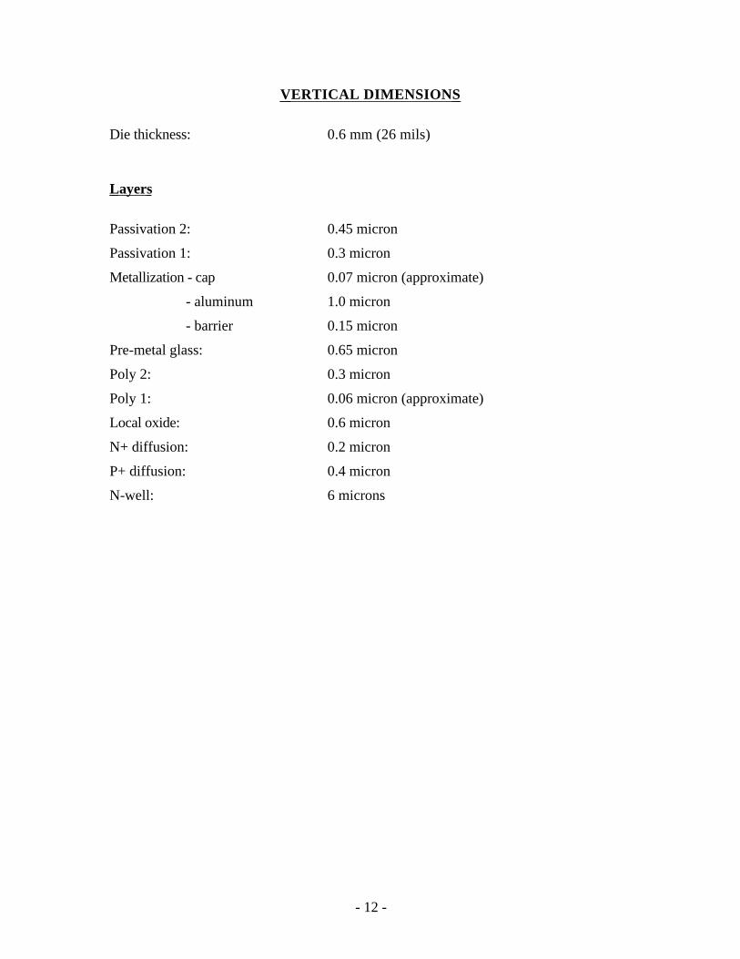
VERTICAL DIMENSIONS
Die thickness: 0.6 mm (26 mils)
Layers
Passivation 2: 0.45 micron
Passivation 1: 0.3 micron
Metallization - cap 0.07 micron (approximate)
- aluminum 1.0 micron
- barrier 0.15 micron
Pre-metal glass: 0.65 micron
Poly 2: 0.3 micron
Poly 1: 0.06 micron (approximate)
Local oxide: 0.6 micron
N+ diffusion: 0.2 micron
P+ diffusion: 0.4 micron
N-well: 6 microns

- ii -
INDEX TO FIGURES
ASSEMBLY Figures 1 - 7
DIE LAYOUT AND IDENTIFICATION Figures 8 - 13
PHYSICAL DIE STRUCTURES Figures 14 - 41
COLOR DRAWING OF DIE STRUCTURE Figure 28
MEMORY ARRAY Figures 29 - 38
CIRCUIT LAYOUT AND I/O Figures 39 - 41
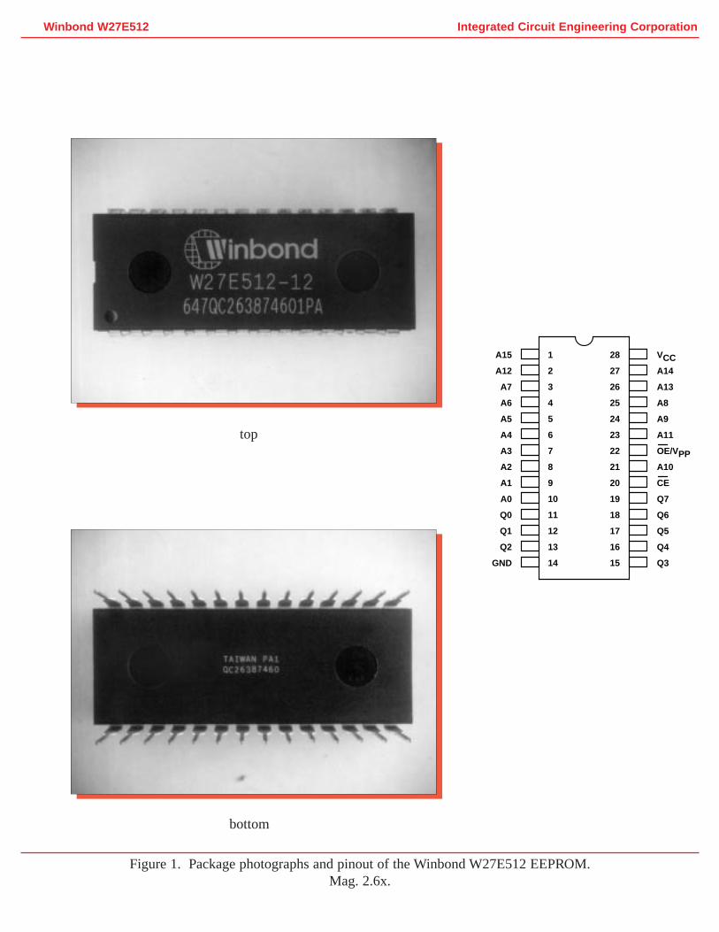
Figure 1. Package photographs and pinout of the Winbond W27E512 EEPROM.Mag. 2.6x.
Winbond W27E512
1
2
3
4
5
6
7
8
9
10
11
12
13
14
28
27
26
25
24
23
22
21
20
19
18
17
16
15
A15
A12
A7
A6
A5
A4
A3
A2
A1
A0
Q0
Q1
Q2
GND
VCCA14
A13
A8
A9
A11
OE/VPPA10
CE
Q7
Q6
Q5
Q4
Q3
top
bottom
Integrated Circuit Engineering Corporation
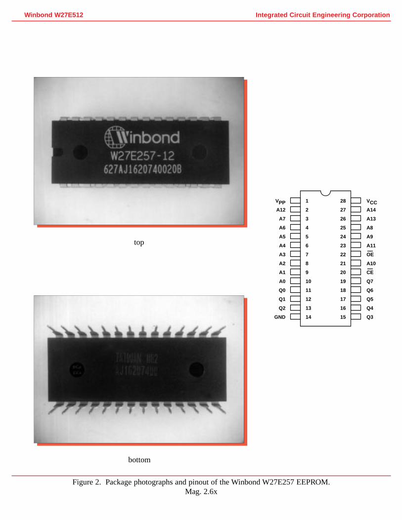
Figure 2. Package photographs and pinout of the Winbond W27E257 EEPROM.Mag. 2.6x
Integrated Circuit Engineering CorporationWinbond W27E512
1
2
3
4
5
6
7
8
9
10
11
12
13
14
28
27
26
25
24
23
22
21
20
19
18
17
16
15
VPPA12
A7
A6
A5
A4
A3
A2
A1
A0
Q0
Q1
Q2
GND
VCCA14
A13
A8
A9
A11
OE
A10
CE
Q7
Q6
Q5
Q4
Q3
top
bottom

Figure 3. X-ray views of the 512K Flash package. Mag. 2x.
Integrated Circuit Engineering CorporationWinbond W27E512
PIN 1

Figure 4. X-ray views of the 256K Flash package. Mag. 2x.
Integrated Circuit Engineering CorporationWinbond W27E512
PIN 1

Mag. 1300x
Mag. 100x
Figure 5. SEM views of dicing and edge seal. 60°.
Integrated Circuit Engineering CorporationWinbond W27E512
DIE EDGE SEAL

Mag. 6500x
Mag. 1600x
Figure 5a. SEM section views of the edge seal.
Integrated Circuit Engineering CorporationWinbond W27E512
PASSIVATION
EDGE OF DIE
PASSIVATION
METAL
POLY 2
Mag. 625x
Mag. 680x
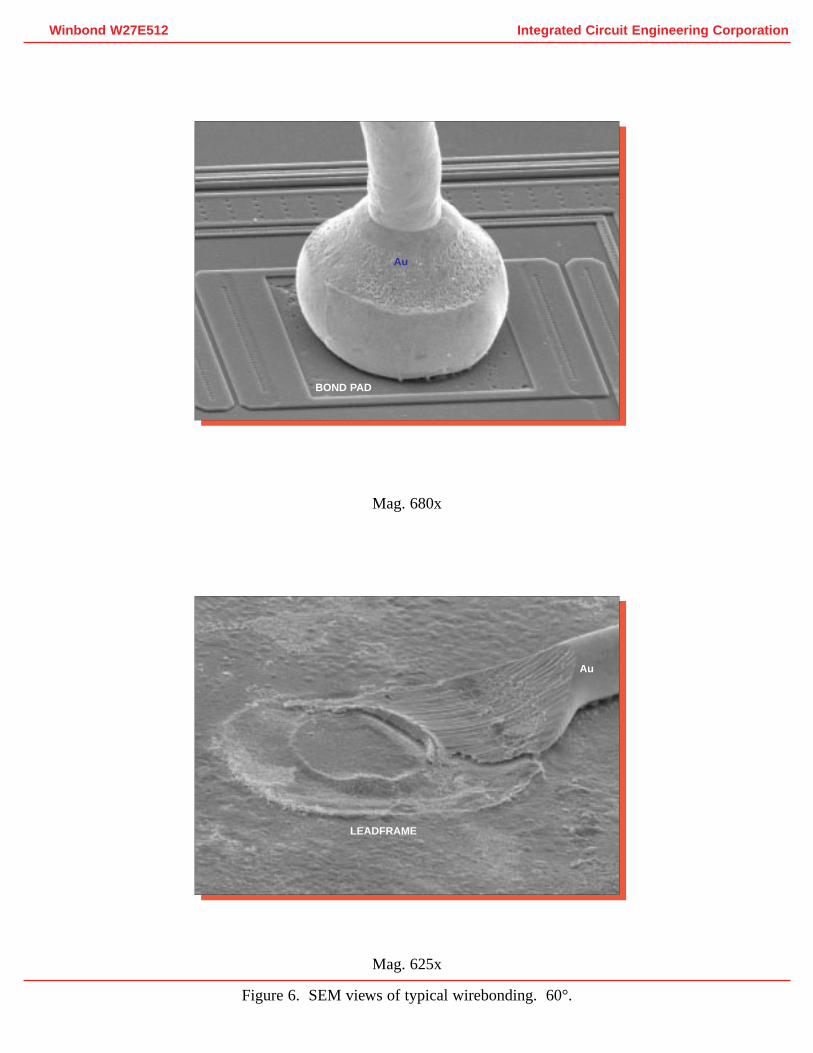
Figure 6. SEM views of typical wirebonding. 60°.
Integrated Circuit Engineering CorporationWinbond W27E512
Au
BOND PAD
Au
LEADFRAME

Mag. 1600x
Mag. 3200x
Mag. 3200x
Integrated Circuit Engineering CorporationWinbond W27E512
Figure 7. SEM section views of the bond pad structure.
Au BALLBOND
Au BALLBOND
PASSIVATION
METAL 1
Au BALLBOND
METAL 1

Integrated Circuit Engineering CorporationWinbond W27E512
Figure 8. Whole die photograph of the Winbond W27E512. Mag. 48x.
Integrated Circuit Engineering CorporationWinbond W27E512
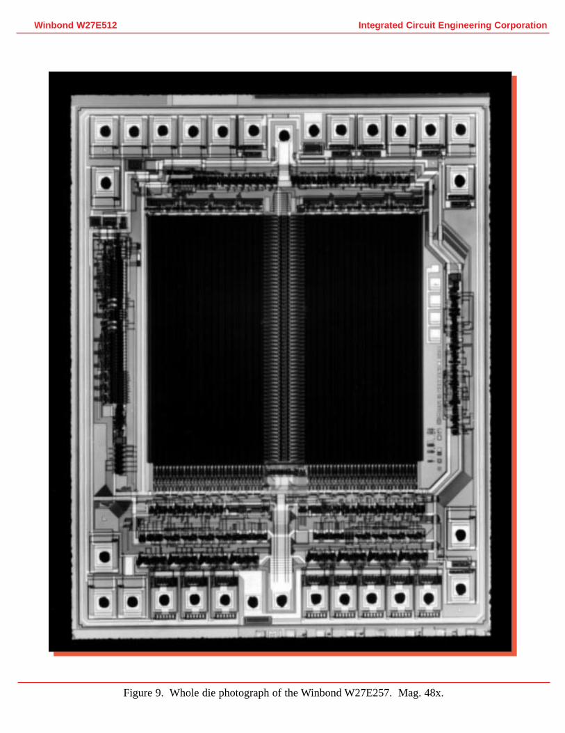
Figure 9. Whole die photograph of the Winbond W27E257. Mag. 48x.

Mag. 500x
Mag. 320x
Figure 10. Optical photographs of markings on the 512K EEPROM die surface.
Integrated Circuit Engineering CorporationWinbond W27E512
Mag. 320x
Mag. 160x
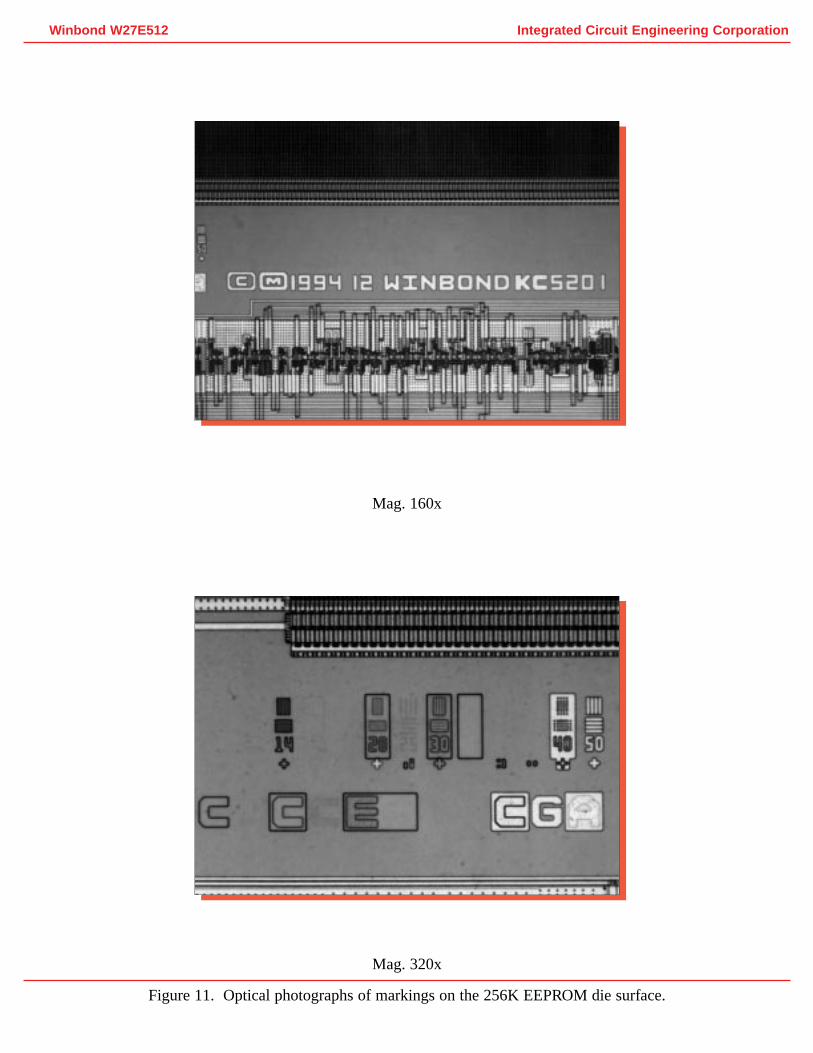
Figure 11. Optical photographs of markings on the 256K EEPROM die surface.
Integrated Circuit Engineering CorporationWinbond W27E512

Figure 12. Optical views of the die corners on the 512K EEPROM. Mag. 100x.
Integrated Circuit E
ngineering Corporation
Winbond W
27E512
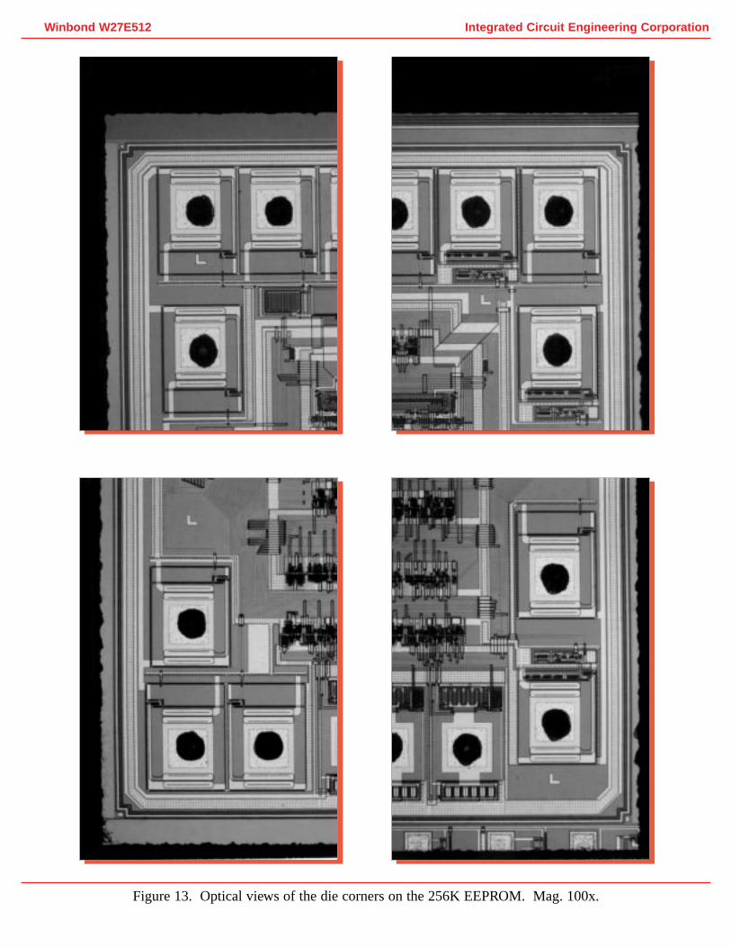
Figure 13. Optical views of the die corners on the 256K EEPROM. Mag. 100x.
Integrated Circuit Engineering CorporationWinbond W27E512

256K
512K
Figure 14. SEM section views illustrating general construction. Mag. 1000x.
Integrated Circuit Engineering CorporationWinbond W27E512
PASSIVATION
METAL
POLY 2
P+ S/D
PASSIVATION
POLY 2
N+ S/D

Mag. 8000x
Mag. 4000x
Figure 15. Perspective SEM views of overlay passivation coverage. 60°.
Integrated Circuit Engineering CorporationWinbond W27E512

Mag. 20,000x
Mag. 13,000x
Figure 16. SEM section views of metal line profiles.
Integrated Circuit Engineering CorporationWinbond W27E512
PASSIVATION 2
PASSIVATION 1
PRE-METAL DIELECTRIC
ALUMINUM
PASSIVATION 2
PASSIVATION 1
ALUMINUM
TiN CAP
TiN BARRIERTi ADHESIONLAYER

Mag. 4400x
Mag. 2200x
Figure 17. Topological SEM views of metal patterning. 0°.
Integrated Circuit Engineering CorporationWinbond W27E512
METAL
METAL
CONTACT

Mag. 13,000x
Mag. 4000x
Figure 18. Perspective SEM views of metal coverage. 60°.
Integrated Circuit Engineering CorporationWinbond W27E512
METAL
METAL
Mag. 26,000x
Mag. 13,000x
Figure 19. Topological SEM views of silicon nodules following the removal of thealuminum. 0°.
Integrated Circuit Engineering CorporationWinbond W27E512
Si
ORIGINALLINE WIDTH
1.5µ
0.6µ
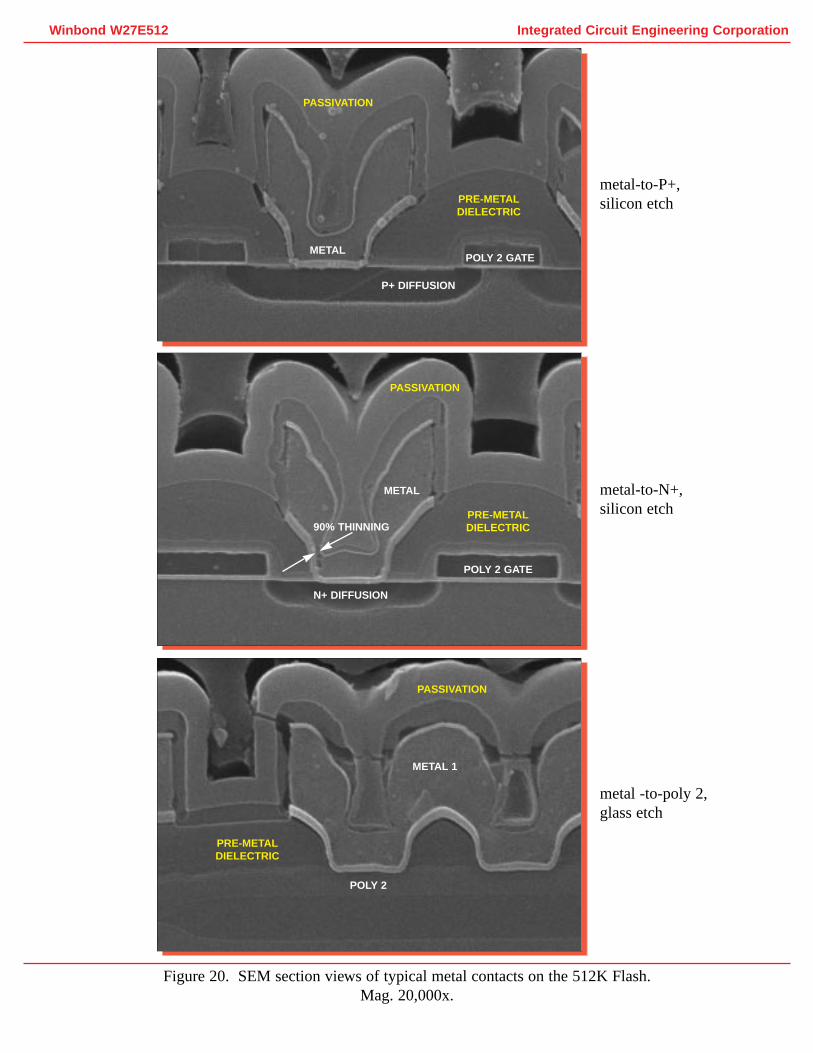
Figure 20. SEM section views of typical metal contacts on the 512K Flash.Mag. 20,000x.
metal-to-P+,silicon etch
metal-to-N+,silicon etch
metal -to-poly 2,glass etch
Integrated Circuit Engineering CorporationWinbond W27E512
METALPOLY 2 GATE
P+ DIFFUSION
PASSIVATION
PRE-METALDIELECTRIC
METAL
POLY 2 GATE
90% THINNING
N+ DIFFUSION
PASSIVATION
PRE-METALDIELECTRIC
METAL 1
POLY 2
PASSIVATION
PRE-METALDIELECTRIC

metal-to-poly 2
metal-to-N+
Figure 21. SEM section views of metal 1 contacts from the 256K EEPROM.Mag. 20,000x.
Integrated Circuit Engineering CorporationWinbond W27E512
POLY 2
METAL
PASSIVATION
PRE-METALDIELECTRIC
POLY 2
METAL
PASSIVATION
LOCAL OXIDE
PRE-METALDIELECTRIC
N+
Mag. 6500x
Mag. 3200x
Figure 22. Topological SEM views of poly 2 patterning. 0°.
Integrated Circuit Engineering CorporationWinbond W27E512
POLY 2
POLY 2
DIFFUSION
Mag. 6500x
Mag. 26,000x
Mag. 26,000x
Integrated Circuit Engineering CorporationWinbond W27E512
Figure 23. Perspective SEM views of poly 2 coverage. 60°.
POLY 2
POLY 2
DIFFUSION
LOCAL OXIDE
POLY 2
DIFFUSION LOCAL OXIDE

P-channel,silicon etch
N-channel,silicon etch
glass etch
Integrated Circuit Engineering CorporationWinbond W27E512
Figure 24. SEM section views of typical transistors. Mag. 40,000x.
POLY 2
P+ S/D P+ S/D
GATE OXIDE
PRE-METALDIELECTRIC
POLY 2
POLY 2
PRE-METALDIELECTRIC
SIDEWALLSPACER
N+ S/D N+ S/D
GATE OXIDE

256K
512K
Figure 25. SEM section views showing the difference in processes of the typicalN-channel transistors. Mag. 52,000x.
Integrated Circuit Engineering CorporationWinbond W27E512
POLY 2
SIDEWALLSPACER
N+ S/D N+ S/D
POLY 2
N+ S/D N+ S/D

Figure 26. SEM section view of a local oxide birdsbeak. Mag. 40,000x.
Figure 27. Optical view of the well structure. Mag. 800x.
Integrated Circuit Engineering CorporationWinbond W27E512
PRE-METAL DIELECTRIC
LOCAL OXIDEPOLY 2
BIRDSBEAK
N-WELL
P-SUBSTRATE

Figure 28. Color cross section drawing illustrating device structure.
Orange = Nitride, Blue = Metal,Yellow = Oxide, Green = Poly,
Red = Diffusion,and Gray = Substrate
Integrated Circuit E
ngineering Corporation
Winbond W
27E512
����������������������������������
���������������������������
������������������������GATE OXIDE
LOCAL OXIDE
P+ S/D N-WELL
N+ S/D
PRE-METAL GLASS
POLY 2
ALUMINUMPASSIVATION 1PASSIVATION 2
P SUBSTRATE
BARRIERCAP

unlayered
metal
Figure 29. Topological SEM views of the Winbond EEPROM cell array.Mag. 6500x,0°.
Integrated Circuit Engineering CorporationWinbond W27E512
METAL
POLY 2
POLY 1
unlayered
metal
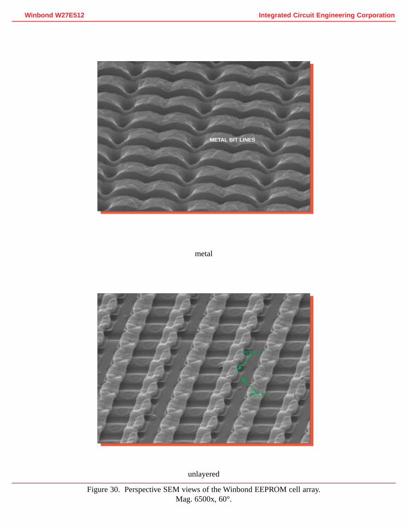
Figure 30. Perspective SEM views of the Winbond EEPROM cell array.Mag. 6500x,60°.
Integrated Circuit Engineering CorporationWinbond W27E512
METAL BIT LINES
POLY 2
POLY 1
unlayered
metal
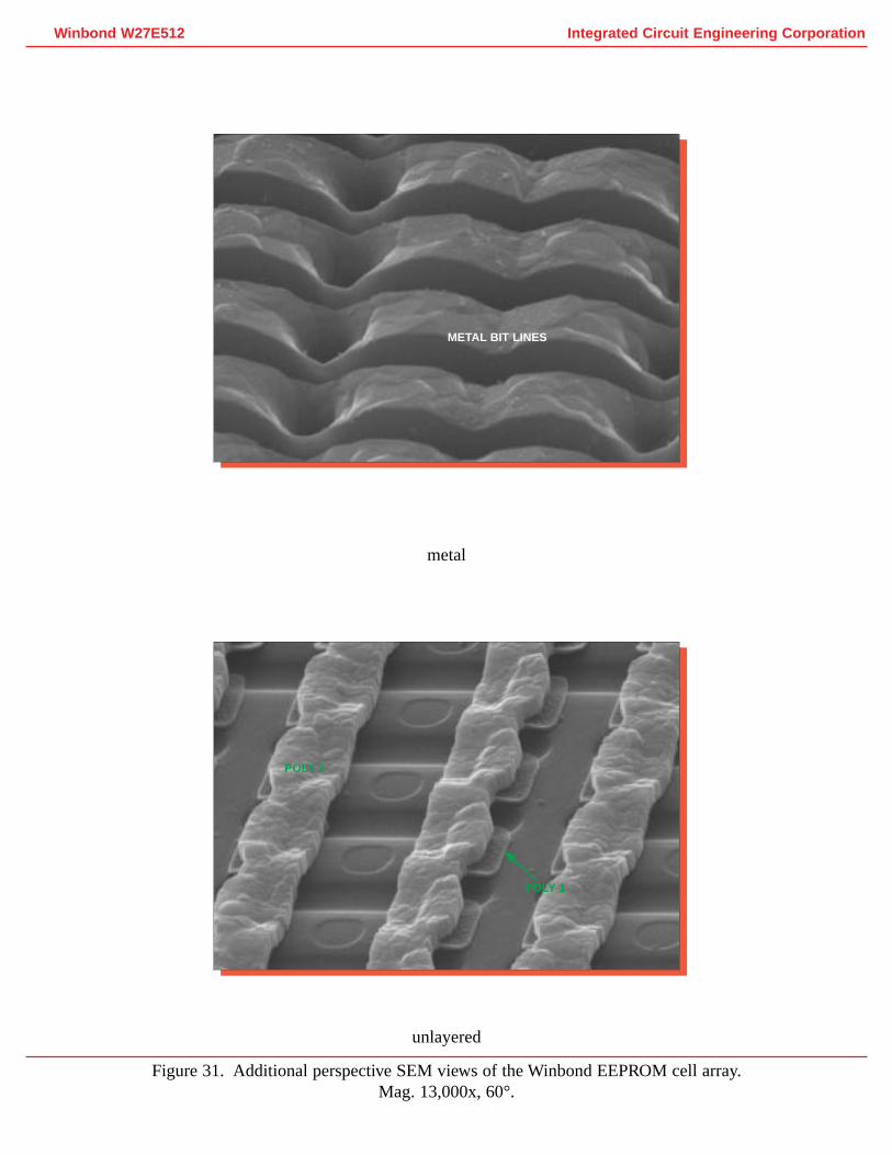
Figure 31. Additional perspective SEM views of the Winbond EEPROM cell array.Mag. 13,000x,60°.
Integrated Circuit Engineering CorporationWinbond W27E512
POLY 2
POLY 1
METAL BIT LINES
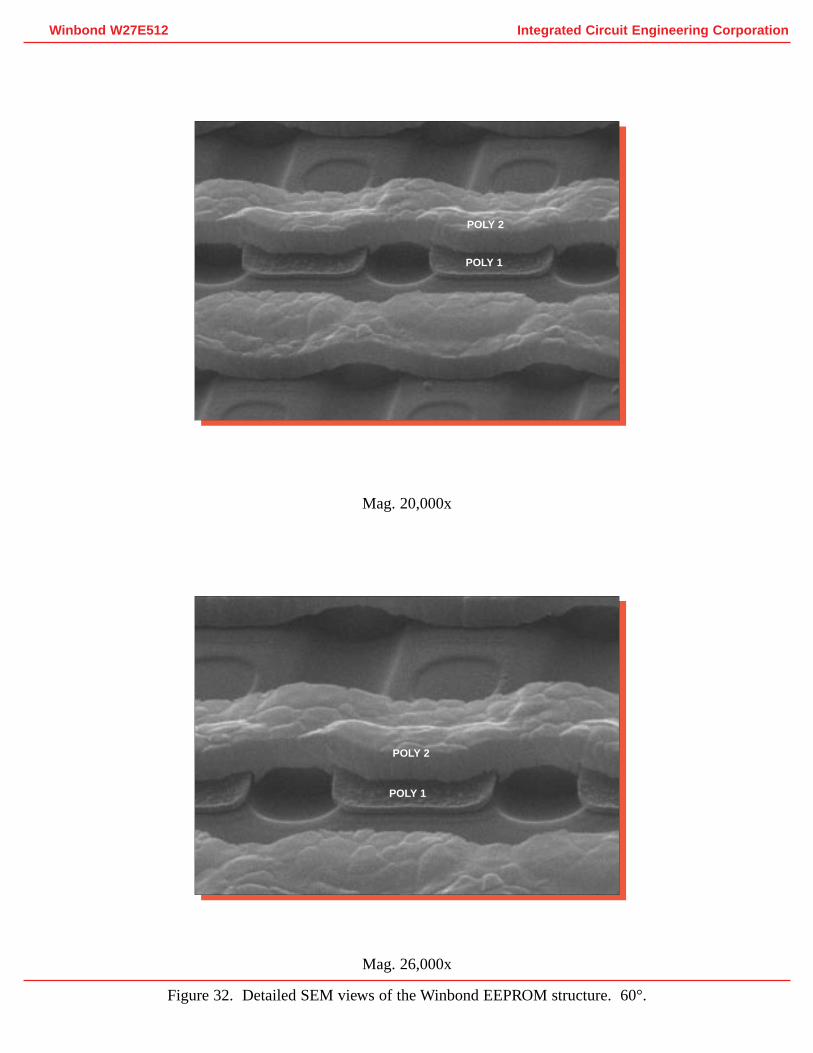
Mag. 26,000x
Mag. 20,000x
Figure 32. Detailed SEM views of the Winbond EEPROM structure. 60°.
Integrated Circuit Engineering CorporationWinbond W27E512
POLY 2
POLY 1
POLY 2
POLY 1

Figure 33. Additional topological SEM views of the Winbond EEPROM cell array.Mag. 13,000x,0°.
metal
unlayered
Integrated Circuit Engineering CorporationWinbond W27E512
BIT
WORD
METAL BIT LINES
POLY 2
POLY 1

glass etch
silicon etch
Figure 34. SEM section views of the Winbond EEPROM cell array(parallel to bit lines). Mag. 6500x.
Integrated Circuit Engineering CorporationWinbond W27E512
METAL
PASSIVATION
METAL
PASSIVATION

glass etch
silicon etch
Figure 35. SEM section views of the metal bit line contacts(parallel to bit lines). Mag. 20,000x.
Integrated Circuit Engineering CorporationWinbond W27E512
N+
POLY 2
POLY 1
CAP
BARRIER
ALUMINUM
PASSIVATION 2
PASSIVATION 1
POLY 2
POLY 1
ALUMINUM
PASSIVATION 2
PASSIVATION 1

Figure 36. Detailed SEM section views illustrating the Winbond EEPROM cell(parallel to bit lines).
Mag. 26,000x
Mag. 52,000x
glass etch,Mag. 52,000x
Integrated Circuit Engineering CorporationWinbond W27E512
POLY 1
POLY 2
N+
PRE-METALDIELECTRIC
METAL BIT LINES
POLY 1
POLY 2
N+
POLY 1
POLY 2
PRE-METALDIELECTRIC
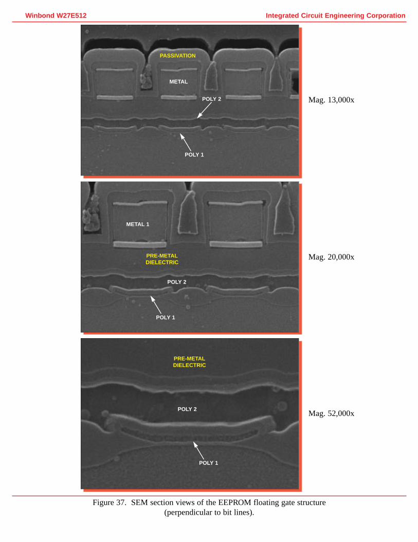
Figure 37. SEM section views of the EEPROM floating gate structure(perpendicular to bit lines).
Mag. 13,000x
Mag. 20,000x
Mag. 52,000x
Integrated Circuit Engineering CorporationWinbond W27E512
PASSIVATION
METAL
POLY 2
POLY 1
METAL 1
PRE-METALDIELECTRIC
POLY 2
POLY 1
PRE-METALDIELECTRIC
POLY 2
POLY 1

Mag. 26,000x
Mag. 15,000x
Figure 38. SEM section views of the metal bit line contacts in the EEPROM cell array(perpendicular to bit line).
Integrated Circuit Engineering CorporationWinbond W27E512
PASSIVATION
LOCOS
METAL BIT LINE
N+
PASSIVATION
LOCOS
METAL
N+
Mag. 800x
Mag. 320x
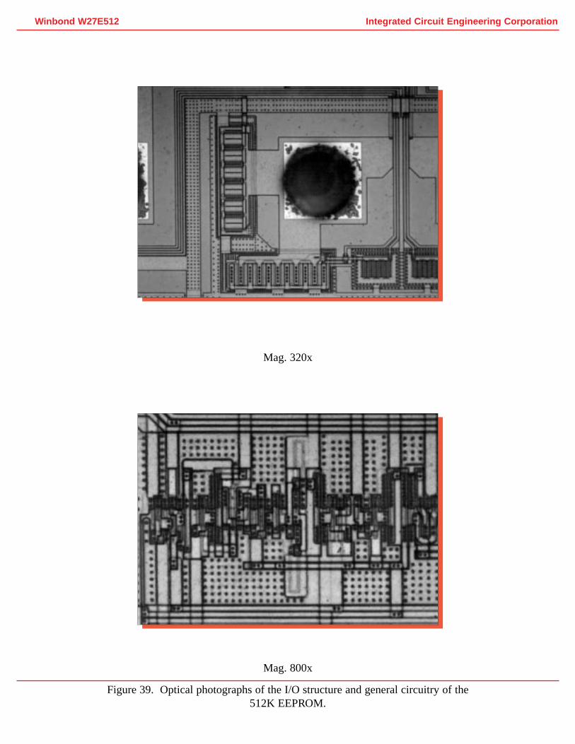
Figure 39. Optical photographs of the I/O structure and general circuitry of the512K EEPROM.
Integrated Circuit Engineering CorporationWinbond W27E512

Mag. 800x
Mag. 200x
Figure 40. Optical photographs of the I/O structure and general circuitry of the256K EEPROM.
Integrated Circuit Engineering CorporationWinbond W27E512
SECTION A(SHOWN INFIGURE 41)
SECTION B(SHOWN INFIGURE 41)

Section B
Section A
Figure 41. SEM section views of transistors at the I/O structure. Mag. 26,000x.
Integrated Circuit Engineering CorporationWinbond W27E512
PRE-METAL DIELECTRIC
POLY 2
N+ S/DN+ S/D
PRE-METAL DIELECTRIC
POLY 2
N+ S/DN+ S/D