wireless technologies and information networks
TRANSCRIPT

International Technology Research Institute World Technology (WTEC) Division
WTEC Panel Report on
Wireless Technologies and Information Networks
Anthony Ephremides, Panel ChairTatsuo Itoh, Vice ChairRaymond Pickholtz, Vice ChairMagdy IskanderLinda KatehiRamesh RaoWayne StarkJack Winters
July 2000
International Technology Research InstituteR.D. Shelton, Director
Geoffrey M. Holdridge, WTEC Division Director and ITRI Series Editor
4501 North Charles StreetBaltimore, Maryland 21210-2699
WTEC Panel on Wireless Technologies and Information Networks
Sponsored by the National Science Foundation, the Department of Defense (OSD), the Defense Advanced ResearchProjects Agency, the Office of Naval Research, the National Institute of Standards and Technology and the National
Aeronautics and Space Administration of the United States government.
Dr. Anthony Ephremides (Chair)University of MarylandRm. 2333AV Williams BuildingCollege Park, MD 20742
Dr. Magdy IskanderElectrical Engineering Dept.University of Utah50 S. Central Campus Dr.Room 3280Salt Lake City, UT 84112
Dr. Tatsuo Itoh (Vice Chair)Dept. of Electrical EngineeringUCLA405 Hilgard AvenueLos Angeles, CA 90095-1594
Dr. Linda KatehiUniversity of MichiganCollege of Engineering2105 Robert H. Lurie Eng. Center1221 Beal AvenueAnn Arbor, MI 48109-2102
Dr. Raymond Pickholtz (Vice Chair)George Washington UniversityDept. EE/Comp. SciencePhillips Hall, 6th Fl.Washington, DC 20052
Dr. Ramesh RaoUCSDDept. of Elect./Comp. Engineering9500 Gilman DriveM/C 0407La Jolla, CA 92093-0407
Dr. Wayne StarkUniversity of Michigan1301 Beal AvenueAnn Arbor, MI 48109-2122
Dr. Jack WintersAT & T Labs Research100 Schulz DriveRed Bank, NJ 07701
Some site reports contained in this volume also were contributed by the following WTEC sponsor representatives:Dennis Friday (NIST), Joanne Maurice (AFOSR/AOARD), Nader Moayeri (NIST), and Leo Young (DOD/OSD).
INTERNATIONAL TECHNOLOGY RESEARCH INSTITUTEWorld Technology (WTEC) Division
WTEC at Loyola College (previously known as the Japanese Technology Evaluation Center, JTEC) provides assessmentsof foreign research and development in selected technologies under a cooperative agreement with the National ScienceFoundation (NSF). Loyola’s International Technology Research Institute (ITRI), R.D. Shelton, Director, is the umbrellaorganization for WTEC. Elbert Marsh, Deputy Assistant Director for Engineering, is NSF Program Director for WTEC.Several other U.S. government agencies provide support for the program through NSF.
WTEC’s goal is to inform U.S. scientists, engineers, and policymakers of global trends in science and technology. WTECassessments cover basic research, advanced development, and applications. Panels of typically six technical expertsconduct WTEC assessments. Panelists are leading authorities in their field, technically active, and knowledgeable aboutU.S. and foreign research programs. As part of the assessment process, panels visit and carry out extensive discussionswith foreign scientists and engineers in their labs.
The ITRI staff at Loyola College help select topics, recruit expert panelists, arrange study visits to foreign laboratories,organize workshop presentations, and finally, edit and disseminate the final reports.
Dr. R.D. Shelton Mr. Geoff Holdridge Dr. George GamotaITRI Director WTEC Division Director ITRI Associate DirectorLoyola College Loyola College 17 Solomon Pierce RoadBaltimore, MD 21210 Baltimore, MD 21210 Lexington, MA 02173

WTEC Study on
WIRELESS TECHNOLOGIES AND INFORMATION NETWORKS
FINAL REPORT
July 2000
Anthony Ephremides, Panel ChairTatsuo Itoh, Vice ChairRaymond Pickholtz, Vice ChairMagdy IskanderLinda KatehiRamesh RaoWayne StarkJack Winters
ISBN 1-883712-58-0This document was sponsored by the National Science Foundation (NSF), the Department of Defense (OSD, DARPA,and ONR), the Department of Commerce (National Institute of Standards and Technology), and the National Aeronauticsand Space Administration of the U.S. government under NSF Cooperative Agreement ENG-9707092, awarded to theInternational Technology Research Institute at Loyola College in Maryland. The government has certain rights to thismaterial. Any opinions, findings, and conclusions or recommendations expressed in this material are those of the authorsand do not necessarily reflect the views of the United States government, the authors’ parent institutions, or LoyolaCollege.

ABSTRACT
This report reviews the status of wireless technologies and information networks around the world, withparticular focus on comparisons between Europe, Japan, and the United States. Specific topics includecoding, modulation and multiple access; switching and routing; channel characterization and propagationmodels; hardware for RF front-end; smart antennas; and holistic design of wireless systems. The studyincludes site reports for visits conducted by panel members to leading research laboratories and universitiesin Europe and Japan. The panel concluded that three major areas of technology must figure prominently inadditional research. These areas include the following: (1) hardware integration and the “system-on-a-chip”; (2) the exploitation of spatial diversity by smart antennas; (3) design by vertical integration onsoftware platforms.
ACKNOWLEDGEMENTS
I would like to thank the U.S. government sponsors of this study: the National Science Foundation, theNational Institute of Standards and Technology (NIST), the Office of the Secretary of Defense (OSD), theOffice of Naval Research, the Defense Advanced Research Projects Agency, and the National Aeronauticsand Space Administration. Special thanks are due to our sponsor representatives who traveled with the panelin Japan and Europe, and who authored many of the site reports included in appendices C and D: DennisFriday and Nader Moayeri (NIST), Leo Young (OSD), and Joanne Maurice (AFOSR). We are very muchindebted to our panel chair, Anthony Ephremides, for his leadership over the course of the study. All of thepanelists are due great credit for their contributions of time and intellect. It was both an honor and a pleasureto work with this group. Finally, we are extremely grateful to all of our hosts in Japan and Europe, and tothe participants in the March 1999 U.S. review workshop, for sharing their activities and insights with us.
Geoffrey M. Holdridge, WTEC Division Director and ITRI Series Editor
International Technology Research Institute (ITRI)R. D. Shelton, Principal Investigator, ITRI Director
George Mackiw, Deputy ITRI DirectorGeorge Gamota, ITRI Associate DirectorJ. Brad Mooney, TTEC Division Director
Robert Margenthaler, BD Division Director
World Technology (WTEC) DivisionGeoffrey M. Holdridge, WTEC Division Director and ITRI Series Editor
Bobby A. Williams, Financial OfficerChristopher McClintick, Wireless Study Manager
Roan E. Horning, Head of Information Technologies SectionMichael Stone, LINUX Systems Administrator
Robert Tamburello, Student Assistant
Judith M. Dobler, EditorAminah Grefer, Editorial Assistant
Jerry Whitman and Stella Lin Whitman, Advance Work for Japan and Europe TripsHiroshi Morishita, WTEC Japan Representative
Copyright 2000 by Loyola College in Maryland except as elsewhere noted. This work relates to NSF CooperativeAgreement ENG-9707092. The U.S. government retains a nonexclusive and nontransferable license to exercise allexclusive rights provided by copyright. The ISBN number for this report is 1-883712-58-0. This report is distributed bythe National Technical Information Service (NTIS) of the U.S. Department of Commerce as NTIS PB2000-105895. Alist of available JTEC/WTEC reports and information on ordering them from NTIS is included on the inside back coverof this report.

i
TABLE OF CONTENTS
Table of Contents ............................................................................................................................................... iList of Figures .................................................................................................................................................. ivList of Tables..................................................................................................................................................... v
Executive Summary....................................................................................................................................... vii
1. IntroductionAnthony Ephremides
Introduction......................................................................................................................................... 1Approach............................................................................................................................................. 2
2. Coding, Modulation, and Multiple-AccessWayne Stark
Overview............................................................................................................................................. 5Background ......................................................................................................................................... 5Coding and Modulation....................................................................................................................... 8Multiple-Access Techniques ............................................................................................................. 12Comparative Analysis ....................................................................................................................... 13Conclusions ....................................................................................................................................... 13References ......................................................................................................................................... 14
3. Switching and Routing in Wireless NetworkingRaymond L. Pickholtz
Preface............................................................................................................................................... 15Introduction....................................................................................................................................... 15Broadband and Internet Access......................................................................................................... 17Concluding Remarks......................................................................................................................... 21Acknowledgment .............................................................................................................................. 22
4. Channel Characterization and Propagation Models for Wireless Communication SystemsMagdy F. Iskander
Introduction....................................................................................................................................... 23Propagation Models for Urban Environment .................................................................................... 24Key Research Issues.......................................................................................................................... 30References ......................................................................................................................................... 30
5. Hardware for RF Front-End of Wireless CommunicationTatsuo Itoh, Linda Katehi
Introduction....................................................................................................................................... 33CMOS Technologies and Silicon Bipolar Transistors ...................................................................... 34III-V Devices and Circuits ................................................................................................................ 37SiGe Devices and Circuits................................................................................................................. 39GaN Devices and Circuits ................................................................................................................. 41Millimeter-wave CPW MMIC .......................................................................................................... 41High Q Components and Filters........................................................................................................ 42Packaging and Integration................................................................................................................. 43

Table of Contentsii
Amplifiers ..........................................................................................................................................47Antennas ............................................................................................................................................48Concluding Remarks..........................................................................................................................49Technology Assessment ....................................................................................................................51
6. Smart AntennasJack H. Winters
Introduction........................................................................................................................................53Smart Antenna Description................................................................................................................53Future Wireless System Requirements ..............................................................................................54Smart Antenna Advantages................................................................................................................55Use Of Smart Antennas .....................................................................................................................55Key Research Issues ..........................................................................................................................55Concluding Remarks..........................................................................................................................57Technology Assessment ....................................................................................................................58
7. Holistic Design of Wireless SystemsRamesh Rao
Introduction........................................................................................................................................59Software Radios.................................................................................................................................59Power and Energy Management ........................................................................................................62Integrated Approaches to Wireless System Design ...........................................................................63Summary............................................................................................................................................64Reference ...........................................................................................................................................64
APPENDICES
A. Professional Experience of Panelists ..............................................................................................65
B. Professional Experience of Other Team Members .......................................................................70
C. Site Reports—Europe
Alcatel................................................................................................................................................72Centro Studi E Laboratori Telecomunicazioni (CSELT)...................................................................74Daimler-Chrysler Research Center, Ulm ...........................................................................................76Ericsson Radio Systems AB ..............................................................................................................80Filtronic PLC. ....................................................................................................................................83GMD FOKUS....................................................................................................................................87German National Research Center for Information Technologies (GMD)........................................90IBM Zurich Laboratory .....................................................................................................................93Institute of Mobile and Satellite Communication Techniques (IMST)..............................................96Nokia................................................................................................................................................102Philips Research Laboratories..........................................................................................................104
D. Site Reports—Japan
Advanced Telecommunications Research-International (ATR-I) ...................................................107Fujitsu Laboratories .........................................................................................................................110KDD Research and Development Laboratories...............................................................................112Matsushita Electric Industrial Co., Ltd ............................................................................................114Matsushita Research Institute Tokyo (MRIT) .................................................................................118Mitsubishi Electric Corporation.......................................................................................................122

Table of Contents iii
Murata Manufacturing Company .................................................................................................... 124NEC C&C Media Research Laboratories ....................................................................................... 129NEC Tsukuba Research Laboratories ............................................................................................. 131Nippon Telegraph and Telephone Corporation (NTT) ................................................................... 134NTT DoCoMo, Wireless Laboratories............................................................................................ 140Tohoku University .......................................................................................................................... 142Toshiba Corporation........................................................................................................................ 144Yokosuka Research Park (YRP) ..................................................................................................... 147
E. Glossary.......................................................................................................................................... 149

iv
LIST OF FIGURES
2.1 The development of a variety of communication systems is shown as a function of data ratesand user mobility/cell sizes. ................................................................................................................... 8
2.2 Possible transmission rates versus signal-to-noise ratios for an additive white Gaussian noisechannel. .................................................................................................................................................. 9
2.3 Received signal strength as a function of time for vehicle velocity 10 mph. ....................................... 102.4 Possible transmission rates versus signal-to-noise ratios for a Rayleigh fading channel. .................... 10
3.1 Four way convergence.......................................................................................................................... 163.2 Vision of a seamless wireless network. ................................................................................................ 163.3 Second generation (GSM/CDMA) network architecture. .................................................................... 173.4 GPRS packet format. ............................................................................................................................ 183.5a GPRS architecture. ............................................................................................................................... 193.5b GPRS network...................................................................................................................................... 193.5c GPRS routing. ...................................................................................................................................... 193.6 Network architecture: Wireless ATM system. ..................................................................................... 20
4.1 Fluctuations of the electric field ........................................................................................................... 254.2 Coverage distribution in an indoor environment. ................................................................................. 264.3 A photograph and schematic diagram of the adaptive/diversity antenna measurement system ........... 264.4 Microcell of delay profile in a parking lot............................................................................................ 274.5 Schematic of the stratospheric wireless access network in Japan. ....................................................... 28
5.1 An example of a silicon-on-anything circuit by Philips Research Laboratory. .................................... 355.2 Double-poly transistor by Philips Research Laboratory....................................................................... 355.3 nMOSFET characteristics by NEC....................................................................................................... 365.4 Transmission lines on an Si substrate used by NEC............................................................................. 365.5 Recent and projected trends for AD conversion for 1990-2002........................................................... 375.6 Daimler-Chrysler InP-based HEMTs. .................................................................................................. 375.7 TRW 190 GHz InP HEMT low noise amplifier................................................................................... 385.8 TRW W-band In-P HEMT power amplifier......................................................................................... 385.9 NEC two-stage mushroom gate HEMT................................................................................................ 395.10 NEC high fmax HBT technology............................................................................................................ 395.11 Comparison of GaAs and SiGe ............................................................................................................ 405.12 World record performance of SiGe HBTs............................................................................................ 405.13 Daimler-Chrysler GaN FET. ................................................................................................................ 415.14 NEC 60 GHz CPW MMIC................................................................................................................... 425.15 A typical flip-chip MMIC structure by NEC........................................................................................ 435.16 Matsushita mm-wave system integration on a chip.............................................................................. 445.17 NTT’s concept on 3D MMIC. .............................................................................................................. 455.18 NTT U-band single-chip down converter............................................................................................. 455.19 NTT K-band Si 3D MMIC examples. .................................................................................................. 465.20 PAE improvement with DC-DC converter by NEC............................................................................. 475.21 Hybrid adaptive predistortion method by Matsushita. ......................................................................... 485.22 NTT’s multi sector monopole Yagi-Uda.............................................................................................. 495.23 NTT’s rod type printed antenna. .......................................................................................................... 49
6.1 Phased array. ........................................................................................................................................ 546.2 Adaptive array. ..................................................................................................................................... 54

v
LIST OF TABLES
ES.1 A Comparison of Wireless Technologies and Networks in Europe, Japan and the United States ......viii
2.1 Comparison of Research Activities ...................................................................................................... 13
4.1a Propagation Models (1998-1999) ......................................................................................................... 294.1b Channel Characterization (1997-1999)................................................................................................. 294.1c Indoor-Outdoor Propagation (1995-1999)..................................................................................... ....... 294.2 Research Activities in the Channel Characterization and Propagation Models in Europe, Japan
and the United States ............................................................................................................................ 30
5.1 Wireless Technology Assessment for Hardware .................................................................................. 51
6.1 Technology Comparison....................................................................................................................... 58

vi

vii
EXECUTIVE SUMMARY
Anthony Ephremides and the Members of the WTEC Panel
INTRODUCTION
What follows is a summary discussion of the current state and trends in wireless communications. Theoverview of this rapidly expanding and technologically diverse field is based on the discoveries of theWTEC panelists during their site visits to leading companies and experts in Europe, Japan, and the UnitedStates as well as the panelists’ expertise in the various areas of wireless communications. Included in thischapter are sections on the major drivers affecting wireless communications growth; a discussion ofbottlenecks, such as systems interoperability, that threaten the development of wireless connectivity; and,finally, a sampling of technology highpoints, including the much-discussed “software radios.”
The findings related in this study were made by the WTEC panelists listed in Appendix A. Table ES.1(p. viii) contains a ratings chart that shows a general comparison of the three regions in the varioustechnologies essential to the field, summarizing this panel’s findings.
U.S. COMPETITIVENESS
On the question of U.S. competitiveness, which of course ranks high in the interests of the sponsors, theincomplete nature of the sampling, and U.S. and foreign reluctance to disclose fully, made a comparativeassessment of capabilities rather difficult. In addition, the corporate world of communications (wireless ornot) is especially globalized and international. It is increasingly difficult to identify national boundaries inthe activities of various companies. As an example, consider the case of Nokia, probably the mostsuccessful manufacturer of cell phones at present, and one of the major players in the arena of wirelesscommunications. Most of Nokia’s long-term research is conducted in Texas, and the overwhelming majorityof its stockholders are U.S. citizens. Yet, the corporate decisions are made in Helsinki.
In any event, the panel made a genuine effort to assess the comparative strengths and weaknesses in theproduction of technologies that are crucial to wireless communications in the United States, in Europe, andin Japan. The reader will find in several of the chapters that follow an evaluation based on numerical scoresthat attempt to characterize the relative position of U.S. industry vis-a-vis that of European and Japaneseindustry. Although the panel is making these disclaimers, it was able, in several cases, to provide such anassessment. Specific assessments that the panel made are summarized in Table ES.1 (p. viii). And, indeed,within each technical area there is some (but not much) variability. However, overall the state ofdevelopment of wireless communication technology in all three regions is very comparable. Thus, it is safeto state that Europe, Japan, and the United States are engaged in a neck and neck race with increasinglyblurred boundaries among their efforts, goals, and achievements.
In the early development of the second generation cellular systems for cellular voice systems (which is onlyone of the multiple facets of wireless), the European Global System for Mobile Communications (GSM)system was an early winner, while Japan was a distant third in the race. Of course, the converging thirdgeneration systems have brought all three regions close to each other. And, as stated earlier, there are manyother aspects of wireless communications in which the regions and industry compete.

WTEC Panel on Wireless Technologies and Information Networksviii
A remarkable observation, however, is that, in a general sense, there is a difference in attitude towardwireless technology development between the United States and Europe, on the one hand, and Japan, on theother. The panel found that in the “Western” world the attitude is preponderantly market-driven, while inJapan it seemed more technology-driven. As a result the panel found an increased readiness and imaginationin Japan to use the technology to develop applications and diverse usages, while in Europe there is a morecautious and conservative attitude. In the United States there is a “happy medium” in that the commercialworld shares the caution of the Europeans, while the military establishment is pushing the frontiers to applyevery available bit of technology and to develop more technology.
Table ES.1A Comparison of Wireless Technologies and Networks in Europe, Japan and the United States
Technology Europe Status Japan Status U.S. Status
Hardware
- mm wave circuits and systems **** ***** **
- Packaging/interconnect *** **** *****
- CAD *** ** *****
- SiGE/Si ***** (Ger.) *** ****
- III-V **** ***** *****
- GaN *** **** ****
- Antennas *** **** ***
- Passive components **** ***** ****
- Amplifier technique **** (U.K.) **** *****
- MEMS ** *** ****
Channel Characterization and Propagation
- Statistical/empirical *** *** ***
- EM based deterministic ** * ***
- Integrative models ** - *
- Microwave and millimeter wave * ** **
Coding, Modulation and Multiple Access ** *** *****
- Multi-user detection theory ** *** *****
- Multi-user detection implementation *** ***** ***
- Coding ***** *** *****
- Multiple access **** **** ****
Software Radios
- Software radio technologies *** *** ***
- Energy efficient communications *** * ***
- Integrated approaches * *** *
* Number of asterixes corresponds to level/quality of activity; more is better

Executive Summary ix
MAJOR DRIVERS OF THE GROWTH OF WIRELESS COMMUNICATIONS
Major factors in the growth of wireless communications include the following:
• personal communications
− the need of increasing numbers of people to communicate with each other anywhere, anytime
− wireless, multimedia delivery
• Internet services
− the expanding need of consumers to access a variety of Internet services without the constraininguse of cable and other wire media
• military and security needs
− the strategic, tactical, and logistical needs to maintain communication in the conduct of operations
• specialized applications
− delivery of services such as telemedicine, replacement of cables at home, at the office, at the factoryor elsewhere, and other untethered applications
MAJOR BOTTLENECKS IN THE DEVELOPMENT OF WIRELESS CONNECTIVITY
The Medium of Wireless Communication
There are two ways in which the medium raises serious technical challenges. The first one is the shortage ofusable bandwidth. The expanding need for high-rate multimedia applications squeezes the availablebandwidth in the frequencies at which propagation properties are favorable. Already most of the spectrumup to the low GHz range is used up. Beyond that, i.e., at Ka-band and beyond, optical phenomena, such asaerosol-induced dispersion, take hold and make communication at long ranges problematic. Yet, if theultimate goals of wireless connectivity are to be realized, the limitations at the higher bands (up to 100 GHz)must be overcome.
The second limitation of the medium has to do with propagation and interference impairments. Multipathpropagation (and the resulting inter-symbol interference), Doppler, shadowing, variable dielectric properties,etc. affect seriously signal strength and decoding ability. In addition, in the presence of multi-usercommunication, interference from other users represents a major obstacle. Of course, already there aretechnology directions that show promise toward overcoming these impairments (such as smart antennas,elaborate MAC protocols, and multi-user detectors); however, much more is needed.
Portability of Equipment
For the ubiquitous use of wireless communication it is necessary that the user equipment (currently referredto as the “handset” or the “palmtop”) be extremely light, small, versatile, and above all, energy efficient.
Battery technology is only one of the means by which the longevity of portable devices can be assured.Pulsed use of the batteries, appropriate circuitry and packaging, directional antennas, suitable modulationand coding, and, most unexpectedly, intelligent network protocols can yield significant energy savings.Furthermore, system integration and space-sensitive design of signal processing algorithms can reduce thesize (and weight) of the portable devices.
System Interoperability
One of the most disabling features in wireless communications is the simultaneous development ofincompatible standards. Even in the widespread application of cellular telephony, the current systems in theUnited States, Europe, Japan, and the rest of the world are simply not compatible. Furthermore, ifconnectivity to the Internet is to be realized, the interoperability of diverse systems, such as satellite

WTEC Panel on Wireless Technologies and Information Networksx
networks, wireless access based systems, the public switched telephone network (PSTN), etc. must beassured. Already progress has been made in the eagerly anticipated, so-called third-generation cellularsystems toward the celebrated goal of convergence. However, interoperability must extend beyond that.
THIRD GENERATION CELLULAR SYSTEMS
The panel found that the major current preoccupations of most companies involved “third-generation”cellular systems. These systems defined most of the immediate concerns and shaped many future ones. Putsimply, the first analog voice cellular systems (exemplified by the U.S. AMPS system) would be the firstgeneration. The digital voice systems that followed (mainly the GSM in Europe and IS-136 and IS-95 in theUnited States) would constitute the second generation while the term “third generation” would refer todigital systems that superpose substantial data services. Of course the path to the third generation has beenevolutionary, and “fractional” systems between the second and third generations can be identified.
The long gestation period that has occurred between generations can be attributed in part to genuinetechnical protocols, but primarily to economic and political difficulties that have to do with market share,intellectual property disputes, and other competitive aspects of product development and service provision.
It does appear certain that within the next couple of years a quantum step in the advancement of wirelesscommunications will have occurred with the launching of third generation systems. But, then the question is“what next?” The panel did ask that question and obtained a variety of answers. Some view as “fourthgeneration” those systems that will be capable of delivering multimedia services at rates upward of 10 Mbpsto mobile users. Such systems will probably need to operate at the higher GHz regions of the spectrumwhere there is ample bandwidth. Others are more skeptical, considering the whole issue of future generationsystems as obscure. However, many of these skeptics are involved in funded studies on the very issue offourth generation systems. Thus, undoubtedly, the next generation of wireless systems ranks high ineveryone's mind. It was interesting that some (especially in Japan) ventured a guess about what the fifthgeneration wireless systems will look like. They presented a vision of unlimited bandwidth and of ratesexceeding 1 Gbps at the 60-90 GHz range for the ultimate realization of global wireless connectivity.
WIRELESS ARCHITECTURES
Many people wonder what wireless architectures, other than cellular and wireless LANs, are possible orachievable in wireless networks. It has been known that at least in the United States, the military has showna keen interest in the so-called “ad-hoc” network architectures. The panel found that although Europe andthe United States showed rather limited interest in ad-hoc networks for commercial applications, there wasmore interest in Japan. Some imaginative applications for the deployment of civilian ad-hoc networks thatinvolve large gatherings, stadium events, etc. were presented. A clear interest in ad-hoc networks of limitedscope for home entertainment was expressed everywhere. The first extremely successful such architecture,which is intended for cable replacement at the office or at home, is the “Bluetooth” standard that hasexperienced overwhelming acceptance in industry worldwide. However, “Bluetooth” is a modest ad-hocsystem. It involves only single-hop access to a “master” station and permits the participation of only up toseven “slave” stations. Especially in home entertainment networks, relaying and multi-hop operation will berequired, since transmission power must be limited (because of a variety of regulatory and practical reasons)and since room and floor partitions induce significant attenuation.
FINDINGS BY TECHNICAL AREA
Within each of the technical areas of the study, the panel reached specific conclusions about the issues thatresearchers here and abroad agree require increased attention. These are reported in detail in the chapters ofthe main body of the report. Here is a brief summary.

Executive Summary xi
Hardware
In the hardware area it is necessary to improve materials, components, and devices. In particular newmaterials such as GaN and SiGe need to be exploited further. In addition, microelectromechanical systems(MEMS) technology can offer advantages in building components. Extensions of the linear region for activedevices as well as improved performance of passive devices are necessary. It is also necessary to developbroadband antennas of higher gain and lower cost phased arrays. In addition, exploitation of 3-D-orientedpackaging technologies offers significant promise.
As far as front-end architecture is concerned, the tradeoff between amplifier linearization and efficiencymust be optimized. Promise also appears in the development of multifunction/reconfigurable devices andcircuits (as well as antennas) in order to facilitate the operation of so-called software-defined radio (a notionthat has emerged as very prominent for the future of the field). Effort is needed to improve interconnectsand packaging, while use of MEMS technology for radio frequency (RF) components promises significantgains.
Expansion of operation in the higher ends of the spectrum (10, 35, 60, 77, and 95 GHz) requires significantbreakthroughs in all aspects of hardware mentioned above. The use of computer-aided design (CAD) toolsfor all-inclusive and interactive packaging that encompasses circuits, devices, and antennas, as well aselectromagnetic, thermal, and mechanical functions, is seen as necessary.
Smart Antennas
In the area of smart antennas, the major improvements needed to realize better coverage and higher data ratesare reduced cost and size (which requires improvements in both electronics and power consumption),increased use of diversity, and better tracking of mobile users. Some of the research directions that holdpromise toward the achievement of these goals are the use of spatial-temporal signal processing algorithms,better and more versatile definitions of standards, and, above all, interdisciplinary, vertically integrateddesigns that incorporate hardware aspects, coding/modulation, access control, antenna directivity, switching,connectivity control, multimedia techniques (such as adaptive compression), and overall systemsarchitecture. In fact, vertical integration emerged as another dominant notion for future wirelesscommunication systems.
Channel Characterization
In the area of channel characterization, it was confirmed that impairments on system performance inflictedby the wireless medium continue to be a major bottleneck in the further development of wirelesscommunications. At a minimum, it is necessary to understand, measure, model, and characterize themedium accurately before developing effective remedies.
As such, the key direction in channel modeling that the panel identified was the coupling of statistical withcomputational (empirical) models. For analysts and designers, the embodiment of channel characteristicsinto a few statistical parameters is very desirable and convenient as it simplifies the enormous task of overallsystem design and evaluation. Such models usually do not provide sufficient accuracy, but, on the positiveside, they are not too dependent on specific environments.
On the other hand, computational models (such as ray tracing) are much more accurate but are verydependent on specific environments and require prohibitive amounts of computation. The only avenue forbetter channel characterizations requires imaginative coupling of these two methodologies. During its studythe WTEC panel did identify vestiges of such coupling already.
WTEC Panel on Wireless Technologies and Information Networksxii
Link Layer
In the area of link-layer operation and design, which includes coding, modulation, and access control, thereare numerous ways in which wireless systems can benefit. After all, this is the most mature area in the“systems” aspects of wireless communication, since it has been the cornerstone of classical point-to-pointtransmission and has triggered the development of the immensely beneficial theories of communication andinformation transfer.
Important directions for research with significant promise for the future include the following:
• improvement of decoding algorithms for turbo codes
• development of new coding/modulation schemes (which could yield large coding gains and permithigher data rates) to reduce the peak-to-mean envelope ratio
• development of coding/modulation techniques that are jointly designed with power amplifiers to extractbenefits both in bandwidth and in energy savings
• development of demodulation/decoding techniques to simultaneously combat the near-far problem anddo channel decoding in multi-rate code division multiple access (CDMA) systems
• better methods of channel estimation at high frequencies
• multiple-access techniques that are driven by different quality-of-service requirements in multi-ratesystems
• analog decoding techniques for high-speed, low-rate systems
In addition, the panel saw overwhelming evidence of the need to couple these techniques with other aspectsof system design and technology that are used in the lower and higher layers of the networking architecture.Thus, space-time coding for multiple antenna systems, hybrid error control methods, joint routing/link-layerdesign, and energy efficiency are examples of integrated approaches that will be necessary for future high-performance, ultra wide band systems.
In other words, again, the panel confirmed the need for vertical integration.
Switching/Networking
In the area of switching/networking, the panel observed the current incompatibility between the availablearchitectures and standards, and the overwhelming attention paid to third generation system design.However, even through the third generation, the air interfaces, the signaling methods, and the handling ofroaming will remain dissimilar and incompatible. The third generation migration of GSM includes apacketized transfer mode (referred to as “general packet radio service” or GPRS). However, theincorporation of Internet Protocol (IP) in wireless networks is fraught with problems. Perhaps a sure way toachieve a short term convergence between wireline and wireless networks is to rely on a connection-oriented, circuit-switched architecture.
The key obstacles (and, hence, research areas) that make this aspect of wireless systems more uncertain andless developed are the lack of understanding of how wireless access impacts the definition of a scalablearchitecture, the lack of suitable protocols for interoperability between the core network and its wirelessextensions, and the difficulty of tracking mobility in real time (mobile IP is not a true mobility trackingprotocol).
Some notions that show promise for resolving these thorny issues involve the expansion of the “intelligentnetwork” (IN) concepts, the imaginative use of distributed databases and algorithms, and, perhaps, a multi-tier architecture that will allow expansion of scale and will permit new services not yet developed or evendefined. Ultimately engineers will need to take a hard look at the possibility of end-to-end IP-based radiosystems.

Executive Summary xiii
Integrated Design
In the area of “holistic,” or vertically integrated design, which emerged as a sufficiently dominant concept togenerate a separate section in the report, the major findings were, as already mentioned, that the developmentof software-defined radios and energy/power management techniques were of foremost interest andimmediate concern.
Software radios are seen, in their early stages, as simply reconfigurable, multimode/multiband radios.However, the extended concept of a software radio involves a wide front end and a totally software-dependent baseband architecture that is capable of configuring the operation of the equipment to conform toalmost any desired protocol, algorithm, or processing structure. Although the realization of such a concept,the most futuristic version of which anticipates downloading to the terminal the code that will define itsoperation in real time, is still years if not decades away, its potential is formidable. Assuming questions ofcost can be resolved (through economics of scale) every mobile user can customize his own terminal to itscurrent environment. And, if questions of cost are not resolved, software radios can reside only at the basestation so that, with their superior “smartness” characteristics, they can adapt their communication to thediverse and simple individual terminals on a one-to-one basis.
Energy savings can be realized in a variety of ways all along the stack of network protocols. From improvedbattery technology and more efficient chip layouts, to better algorithms for signal processing and adaptiveantenna arrays, to improved coding/modulation techniques, to power management techniques in mediaaccess control, numerous avenues are available to increase the longevity of untethered terminals andequipment and to save operational and thermal costs at base stations. What is new is the realization that inaddition to these methods, network protocol design can have a significant impact on energy efficiency.From pulsed operation of batteries (as for example in time division multiple access—TDMA—schemes) tointelligent routing and multicasting, network protocols can create substantial energy savings. Furthermore,in addition to transmission energy expenditures, there is energy consumed for processing and for simplybeing “on.” Thus, schedules of alternating between “sleep” and “on” modes (as in current paging systems),joint design of compression and transmission schemes, etc., provide means for better overall energyefficiency.
A SAMPLING OF TECHNOLOGY “HIGH-POINTS”
Since this study was performed as an “assessment” of current and future technology, and since its conductinvolved numerous site visits around the world, it is appropriate to summarize a few of the dominant pointsof high technology that the WTEC panelists observed.
The widely espoused notion of “software radio” was a common theme throughout the site visits. The panelwas struck by the variety of levels at which this notion is conceived in different quarters. From the simplestversion of multi-mode/multi-band radios presented at Ericsson to the most imaginative versions encounteredelsewhere, it was clear that this will be the way of the future.
The integration of the antenna into the handset, seen at Nokia, was another harbinger of the direction offuture development.
The panelists even saw silver-plated sets that permit the installation of the antenna inside the terminalthrough a thin-strip plastic window. A great deal of design effort was needed in shaping the antenna plate.
The availability of polymer batteries, displays, and electronics, seen at Philips, is another harbinger of thingsto come. In addition to reducing weight and costs, these promise superior performance. The first integratedchannel characterization models, seen again at Philips, combine electromagnetics, statistics, and computationto provide useful and reasonably accurate models of channel behavior.

WTEC Panel on Wireless Technologies and Information Networksxiv
The packaging techniques at Matsushita were clearly indicative of superior achievement in the hardwareaspects of wireless communication.
The development of three-dimensional integration at Nippon Telegraph and Telephone (NTT) clearly pointsthe way toward size and weight reduction as well as improved performance.
At many sites (especially NTT) the panel was impressed by the effort being made toward reducing the costof phased arrays.
The SKYNET concept outlined at Yokosuka Research Park (YRP) in Japan is an impressive example ofimaginative wireless networking. It is based on a small number of large balloons, suspended in thestratosphere and kept in place by solar-powered propellers, that permit the installation and support ofmultiple antennas of various sizes. Through direct link connection to terrestrial sites and users, coveragespans the entire region of Japanese territory. Thus, a constellation of satellite-like base stations creates anadequate and relatively inexpensive infrastructure for wireless connectivity.
Study team members were also impressed by the actual deployment of a multi-user detector that utilizessuccessive interference cancellation in CDMA systems. Although the theory of multi-user detection is quitemature by now, concerns about cost and implementation have held back the incorporation of advanceddetectors in actual systems. At NTT DoCoMo, the developed system was at the stage of actual field trialsand tests.
Last, but not least, the panel found the advanced miniature multimedia terminals at NTT DoCoMo veryimpressive and, also, forerunners of future development.
CONCLUSIONS
It is difficult to summarize the findings, observations, and impressions of such a vast study of such anevolving discipline into a few concrete nuggets. Yet, it became clear to this panel that, after the dust hadsettled, three major items stood out as the major areas of future technology that require significant additionalresearch. These include the following:
• the hardware integration that will realize the notion of a “system on a chip”
• the overwhelming need to exploit spatial diversity by means of smart antennas
• vertical integration of protocols in the design of software radio platforms
All three stood out as being dominant concerns of all visited companies and institutes, both in the UnitedStates and abroad. It is also the unanimous and informed belief of the WTEC study team that resolving theseissues is necessary in order to realize the ambitious goal of global wireless connectivity.

1
CHAPTER 1
INTRODUCTION
Anthony Ephremides
INTRODUCTION
Rapid growth in wireless communications has recently stimulated numerous studies, workshops, reports, andother activities. All aim at fostering broad appreciation and understanding of the field as well as atformulating appropriate responses to trends in the development of related products and services. The WTECstudy was sponsored by an impressive number of agencies of the U.S. government, led by the NationalScience Foundation. In fact, it was during a workshop sponsored by NSF in the summer of 1998 that arecommendation emerged to sponsor such a study. The objective was to assess long-term trends in researchin the wireless communications area worldwide. A corollary objective was to use the findings to betterformulate research funding priorities for the U.S. agencies that will help promote and maintain thecompetitiveness of the United States in this important technology area.
This introductory chapter describes the general parameters of the study and the approach that this panel tookin addressing the sponsors’ charge.
The first realization was that the field of wireless communications has multiple facets. To some people itconjures simply the image of cellular telephony and to others only propagation or fading phenomena. To themembers of the WTEC panel, it represents the full gamut of applications that encompass cellular telephony,wireless LANs, Internet access, personal communications, telemedicine, other specialized applications, and,last but not least, military communications (which include diverse uses with corresponding uniquerequirements). It also encompasses, from the technology point of view, all the issues that traditionallycorrespond to the seven layers of the open systems interconnection (OSI) architecture that has governed thefield of communications and networking in the last third of the 20th century.
This realization influenced the selection of the researchers and scientists who composed this panel, whichcontained truly distinguished experts and recognized authorities at all levels of the OSI model.
The second realization was that the task was enormous in light of the resources of the study. There has beensuch an intense and expansive growth in the field that almost every major company in the industrializedworld, as well as literally hundreds, if not thousands, of mushrooming small players, have entered thetechnology and service arenas in this field. To fully access the status of wireless communications in theworld, the panel would have to engage in an impossible mission of visits and meetings, which, in addition tobeing prohibitively expensive, would require a length of time that would render the findings obsolete by thetime the study concluded.

1. Introduction2
Thus, the panel decided to be selective. It concentrated on major companies and institutes and carefullyselected a representative set in the United States, Europe, and Japan.
The third realization was that applications are often ahead of theory and have been leading the developmentof technology. As a result, the enormous financial stakes have created a very intense competitiveenvironment among the world’s major players. In turn, this has diminished the willingness to share not onlycurrent research and development plans but also longer-term plans.
Therefore, the panelists had to challenge their skills to infer the directions in which companies see the fieldevolving.
A related realization was that the rapidity with which the wireless technology is used in a variety of newapplications has created an environment in which confusion (if not chaos) is common. Not only the generalpublic but also the technology developers themselves lack a firm, commonly held vision as to what isimportant (both in terms of products as well as in terms of services).
Consequently, the panelists had to use their own expertise and understanding of the field to interpret andcomplement the inputs they received.
Finally, the panel members realized that the community is paying a great deal of attention to the physical,link, and media access control (MAC) layers in the field of wireless communications. This is the result ofpreviously dominant needs in military communications (that have led and predated the development ofcommercial applications by many years) and in cellular communications.
Because of the emphasis on layering and because the panel members firmly believe (as do most of therepresentatives of the sites it visited) that in wireless communications, hardware and networking aspects willbecome increasingly important, if not dominant in the future, the panel decided to focus on all seven layersof the OSI architecture as well as on antennas and equipment.
APPROACH
Based on the framework that emerged from these realizations during the early part of the study, the paneldeveloped a plan that included a schedule with specific benchmarks as well as a strategy for approaching thesubject. The goal was to maximize the efficiency of the data-gathering phase and to formulate a concept thatwould be true to the overall framework.
Thus, the schedule of activities was organized as follows. It commenced with a kick-off meeting of thepanel (jointly with sponsors) in January 1999 in the Washington, DC area, during which the panel unfoldedits strategy. A technical workshop followed in the Washington, DC area on March 15, 1999, in which mostmajor U.S. companies active in the wireless communications area were invited to participate. The panelchose to canvas U.S. industry opinion in this manner (rather than through individual visits) purely forreasons of efficiency. Thirteen companies (listed elsewhere in the report) contributed inputs based on aquestionnaire that the panel developed and forwarded to them ahead of time. The collection of viewgraphsfrom their presentations became (and still is) available from WTEC as a separate document.
Following that the panel took two weeklong trips to Europe and Japan, respectively, where it visited a totalof 24 companies and institutes. These visits took place in April, May, and early June 1999. The intensity ofthe schedule necessitated splitting the group (consisting of panel members and of representatives of some ofthe panel’s sponsors) into subgroups. Thus, no single individual in the group enjoyed first-hand contact withall of the visited sites. Shortly after the completion of these visits, a separate report for each site wasgenerated, authored by a pre-designated member of the group but in wide consultation with and inputs fromother panel members. These reports were sent to the visited sites for concurrence and, after revisions to

Anthony Ephremides 3
account for hosts’ comments, became available on the WTEC Web site. They are now included, after finalediting, as appendices C and D of this report.
At this point the panel needs to mention that representatives from some of the sponsoring agencies played avery active role in participating in the conduct of this study. Through their membership in the travel group,authorship of site-visit reports, and active deliberation with the panel, they provided valuable assistance inshaping the outcome of the study.
Exactly because the site visit reports were generated as separate documents, the panelists felt that thestructure of the main analytical report should not follow the format of reporting findings from each site.Rather, it was decided to structure the report on the basis of technical areas.
Thus, the specific elements found at a particular site, as they pertained to one technical area, would be fusedinto the discussion of that area along with the appropriate elements found in other sites. In this way, thepanel members believe they have produced a more informed and informative report that will be more usefulto sponsors and to the community at large. In addition, under that structure, the findings would be consistentwith the principles of the framework outlined in the introduction.
In deciding what technical areas to choose so as to form a spanning skeleton for the entire field, it wasnatural to follow the OSI layered architecture. Nevertheless, it is interesting to note that one of this panel’smajor findings is that the traditional separate consideration of networking layers is less useful in the wirelessarea. Indeed, the technical coupling among layers, always present even in nonwireless networks, is simplytoo strong in wireless systems to be ignored. The convenience that separation into layers provides is in largemeasure due to the fact that it ignores the interactions among layers. In wireless networks this convenienceis countered by the neglect of crucial interactions (between multiple access and routing or between linkcontrol and compression, for example).
However, structuring the report along traditional layer lines does not contradict this finding. It simplypermits a clean organization of the report. In fact, relationships among the layers are duly noted andreported as these arise. Thus, the chapters that follow in the main body of the report are centered,respectively, on the following topics:
• hardware (i.e., materials, devices, circuits, amplifiers, antennas, and system integration that optimizeefficiency in wireless communication)
• antennas and signal processing (i.e., the “systems” aspects of antennas, including spatio-temporalprocessing to combat fading and interference and to shape adaptively the antenna patterns)
• channel modeling (i.e., statistical and empirical models that predict propagation patterns and signalattenuation)
• modulation/coding/access (i.e., link-layer issues that govern quality of point-to-point transmission)
• networking/switching (i.e., architecture and higher-layer issues that affect quality of service system-wide)
• integrated/holistic design (i.e., a novel viewpoint that starts from the realization of inter-layer couplingand exploits the possibilities of software-defined radios, energy efficiency, and other issues that cutacross layers)
After a brief gestation period following the site visits and the composition of the site-visit reports, the panelheld a final open workshop to disclose the preliminary findings of the study. This workshop was held in theWashington, DC area in September 1999 and was attended by a large audience. The collection ofviewgraphs from the presentations by the panelists and the sponsors were posted on the WTEC Web siteshortly after the workshop (now superceded there by this final report). The present report constitutes thefinal step in this study.

1. Introduction4
5
CHAPTER 2
CODING, MODULATION, AND MULTIPLE-ACCESS
Wayne Stark
OVERVIEW
The goal in wireless communication systems is to provide mobile, fully integrated, low cost, reliable,seamless systems with the capability of providing voice, high speed data, and video with minimum latencyand long battery life. However, there are many obstacles and bottlenecks to achieving this in practice.These bottlenecks include the following:
• limited spectrum
• limited energy
• multipath fading and propagation loss
• cost
• standardization processes
This chapter of the report focuses on coding, modulation, and multiple-access techniques for wirelesscommunications. To put the discussion in perspective, a short background on the development of wirelesscommunication systems, focusing mainly on cellular systems is provided. The following sections discusscoding and modulation and various modulation techniques; present a comparative analysis of research anddevelopment in Europe, Japan, and the United States; and, finally, make recommendations for furtherresearch in wireless communications.
BACKGROUND
Cellular Systems
Wireless communications became a commercial success in the early 1980s with the introduction of cellularcommunication systems in the United States, Japan, and Europe. All of these systems were based onfrequency division multiple-access whereby a user during a call was assigned a given frequency fortransmission to a base station (uplink) and a given frequency for reception from the base station (downlink).The modulation technique adopted was frequency modulation (FM) for the voice signal. The bandwidthassigned to each user was around 30 kHz (depending on the country). Frequency division multiple access(FDMA) and FM modulation were well known techniques/technology available to system designers at thetime. It is interesting to note that a university professor in the early 1980s actually proposed code divisionmultiple-access (CDMA) as a technique for cellular communications, but AT&T/Bell Labs (pre-divestiture)discredited it. At the time digital technology was not ready for a modulation technique requiring

2. Coding, Modulation, and Multiple-Access6
sophisticated processing algorithms. Nevertheless, the basic research component of this effort affectedfuture wireless communication systems.
The designers of cellular systems faced many challenges that were unique to mobile environments. Thesechallenges included time-varying multipath fading and interference from other users. The problem ofmultipath fading was handled by simply increasing the amount of transmitted power. Most of the cellphones were mounted in cars, handheld units were not available, and battery power was not the initialdriving force. Interference was minimized by not reusing a given frequency in an adjacent cell. Finally, theapplication was purely voice communications.
In Europe, many different first generation systems operated in different frequency bands, and thus roamingbetween countries was not possible with a single cell phone. This lack of interoperability in Europe was oneof the key drivers towards developing a second generation system in Europe. In the United States, theincreased use of cell phones in the mid-1980s led to a shortage of capacity in major markets (Los Angeles,New York, Chicago). In order to achieve higher capacity (users/cell/Hz) second generation systems begandevelopment in the mid-late 1980s. Second generation systems (in the United States, Europe, and Japan) areall based on digital transmission techniques whereby the voice signal is encoded into a sequence of bits. Thevoice-coded data is then encoded for error correction and modulated using digital modulation techniques.Going to a digital modulation technique has several advantages, including the spectral efficiency of digitalmodulation, the capability of combining speech and data services, and the improved security of digitaltechniques. The first proposal for second generation systems in the United States was based on time-divisionmultiple-access (TDMA) whereby each 30 kHz of bandwidth was slotted in time so that three users coulduse the same spectrum. This was possible because of the compression algorithms applied to speechwaveforms. In these systems error correction was introduced to mitigate the effect of multipath fading.Interference is not a predominant issue in this design as different users use either different frequency or timeslots or nonadjacent cells. Like first generation systems, essentially the only application for secondgeneration systems (both cellular and personal communication systems (PCS) that use the 1900 MHzfrequency band) is voice, although some low speed data communication capabilities are also possible.
It is interesting to note that the modulation technique chosen in Europe (Gaussian minimum shift-keying) forsecond generation systems is a constant envelope technique while the modulation technique chosen in theUnited States and Japan is π/4 differential phase shift keying (DPSK) with raised cosine filtering, which is anonconstant envelope technique. Constant envelope techniques ensure that the envelope of the transmittedsignal is a constant. This fact allows the power amplifier used by the mobile system to operate nearsaturation without distorting the signal. The most energy efficient operation of an amplifier is nearsaturation as this is when the power added efficiency is largest. The disadvantage of constant envelopemodulation techniques is that their bandwidth efficiency is small relative to modulation techniques that havefluctuating envelopes. On the other hand nonconstant envelope modulation techniques need very linearamplification in order to preserve the signal shape (no distortion). Nonlinearities applied to a nonconstantenvelope technique create both adjacent channel power and in-band intermodulation distortion. The adjacentchannel power essentially widens the bandwidth occupancy of the signal while the in-band intermodulationdistortion acts like additional noise in the system. No distortion is incurred when linear amplification is usedwith nonconstant envelope modulation techniques. However, linear amplification is possible mainly byoperating the amplifier with a small input signal (large backoff) where the energy efficiency of the amplifieris smallest. This characteristic of nonlinear amplifiers makes large power efficiency and bandwidthefficiency hard to achieve simultaneously.
In the late 1980s Qualcomm made a proposal to use direct-sequence spread-spectrum multiple-access (alsocalled code division multiple-access) for cellular systems. Qualcomm’s initial claims of significant (morethan 10 times) increase of capacity of cellular systems captured the attention of service providers. This effortdeveloped into a later second generation standard known as IS-95. The increase in capacity, it was claimed,was due to exploitation of the voice activity factor, Rake reception, which allowed exploitation of themultipath fading and frequency reuse of 1 (every cell uses all frequencies), which allowed more efficient use

Wayne Stark 7
of the frequency spectrum over a geographical area. In addition, multiple users spreading their signals over awide bandwidth with user unique codes allowed for multiple users using the same spectrum at the same time.The IS-95 system uses 1.25 MHz of spectrum. The IS-95 system first became available commerciallyaround 1995.
A significant event for wireless communication systems occurred in the mid-1990s when the FederalCommunication Commission (FCC) decided to auction off spectra in the 1.9 GHz band. This opened up apair 60 MHz frequency bands between the 1850-1910 and 1930-1990 MHz spectra for use by those withwinning bids in the auction. This band was called the personal communication system (PCS) band, andsystems operating in this band are called PCS systems. The modulation and coding techniques that werechosen for these systems were virtually all-cellular type systems except they were shifted up in frequency.The operating characteristics (coding, modulation, and multiple-access) were identical. Nevertheless thisprovided additional capacity for wireless communications and allowed for increased competition.
The overall goal of first and second generation systems is primarily voice communications. The innovationsbetween first and second generations were mainly in going to digital modulation techniques and the use oferror control coding. Third generation systems are now being designed and implemented to handle not onlyvoice but high speed (from 384 kbps to 2 Mbps) data, although no one really knows what the market forthese services will bear.
Other Wireless Systems
Cellular communication systems are clearly the most widely used wireless communication systems.However, other systems have different characteristics that deserve mentioning. To begin with, manymilitary communication systems need to operate in a very different type of environment. First, in a militarycommunication system, there may not be the possibility of dividing a region into cells and deploying a basestation in each cell. Military systems tend to be highly mobile and may possibly operate in unfriendlyenvironments where the cellular type of deployment is not possible. Military systems must also face thepossibility of hostile interference (jamming). One of the consequences of not having base stations is thatrelaying messages is required. In other words, multihop communications over multiple wireless links isnecessary. This creates a whole new class of communication problems and constraints.
Another wireless communication system of interest is a wireless local area network (WLAN), whereby awireless link replaces the wired LAN. Currently such systems tend to operate in the Industrial-Scientific-Medical (ISM) band (902-928 MHz, 2400-2483 MHz, 5725-5780 MHz). This band is available forunlicensed use (in the United States) provided either the power levels are small enough or spread-spectrummodulation techniques are employed with larger transmitted power. The 2.4 GHz band is available world-wide while the 900 MHz band is not available is some parts of the world (e.g., Europe).
Another wireless system gaining significant attention is a cable replacement wireless system calledBluetooth. This is being developed by a consortium of communications and computer companies (e.g.,Ericsson, Nokia, IBM, Intel, Motorola). The objective of a Bluetooth system is to replace the cablesconnecting different components in a computer system with wireless links. Because it is a cable replacementthe objective is for a very low cost, low range system. It is also viewed as a means for connecting a mobilecomputer with a cell phone in a wireless manner such that communication between the mobile computer anda hidden (e.g., in the briefcase) cell phone can be used to connect to the Internet. It can also connect aheadset to a cell phone without wires. The range is about 10 meters with 0 dBm (1 milliwatt) transmittedpower, but can be increased to 100 meters with larger power. Bluetooth uses the 2.4 GHz ISM band withfrequency-hopped spread-spectrum. The maximum data rate is 721 kbps. It handles up to 8 devices in a so-called “pico-net” and can have up to 10 pico-nets operating in a coverage area. The networks created withBluetooth are ad-hoc networks implying multiple-hops per end-to-end connection.
A competing system is HomeRF. HomeRF is geared more towards higher data rates and higher transmittedpower. As with Bluetooth, HomeRF is a frequency-hopping system operating in the 2.4 GHz band.

2. Coding, Modulation, and Multiple-Access8
Products with data rates in the range of 2 Mbps with operating distances on the order of 150 feet arepossible.
The development of a variety of communication systems is shown in Fig. 2.1 as a function of data rates anduser mobility/cell sizes. This figure illustrates the fact that higher data rates are possible at lower mobilitiesor decreased cell size. This is due to two considerations. The first (and main) consideration is that at smallerdistances the propagation loss is less and thus for a given power level, higher values of Eb/N0, the receivedsignal-to-noise ratio, are possible. Another effect is that at high mobilities the channel is harder to estimateand thus proper demodulation/decoding becomes more difficult. This is compensated for, to a certain extent,by the fact that generally error control coding works better (for a fixed block length) when the channel ismemory-less (independent fading on different symbols).
Cel
lula
r
Pagi
ng
Home RFBluetooth
High SpeedData
(MMAC)
IMT-2000,3G Cellular,
W-CDMA
4-thGeneration
Cellular
Ultra High
Speed LAN
60 GHz?
Data Rate (bps)
Mob
ility
/Cel
lsiz
e
10k 100k 1M 10M 100M
Indo
orPe
dest
rian
Veh
icul
ar
Fig. 2.1. The development of a variety of communication systems is shown as a function ofdata rates and user mobility/cell sizes.
CODING AND MODULATION
Coding and modulation provide the means of mapping information into waveforms such that the receiver(with an appropriate demodulator and decoder) can recover the information in a reliable manner. Thesimplest model for a communication system is that of an additive white Gaussian noise (AWGN) system. Inthis model a user transmits information by sending one of M possible waveforms in a given time, period T,with a given amount of energy. The rate of communication, R, in bits per second is log2(M)/T. The signaloccupies a given bandwidth W Hz. The normalized rate of communications is R/W measured inbits/second/Hz. The received signal is the sum of the transmitted signal and white Gaussian noise (noiseoccupying all frequencies). The optimum receiver for deciding which of the M signals was transmittedfilters the received waveform to remove as much noise as possible while retaining as much signal aspossible. For a fixed amount of energy, the more waveforms (the larger M) the harder it is for the receiver todistinguish which waveform was transmitted. There is a fundamental tradeoff between the energy efficiencyof a communication system and the bandwidth efficiency. This fundamental tradeoff is shown in Fig. 2.2.In this figure the possible normalized rate of transmission (measured in bits per second per Hz) is shown as afunction of the received signal-to-noise ratio Eb/N0 for arbitrarily reliable communication. Here, Eb is theamount of energy received per information bit while N0 is the power spectral density of the noise. Thecurves labeled AWGN place no restrictions on the type of transmitted waveform except that the averageenergy must be constrained so that the received signal energy per bit is Eb. The curve labeled BPSK restricts

Wayne Stark 9
the modulation (but not the coding) to binary phase shift keying. The curve labeled QPSK is for quaternaryphase shift keying and the 8-PSK curve is for 8-ary phase shift keying. Clearly at low rates and low Eb/N0
there is virtually no loss in using QPSK modulation with the best coding compared to the best modulationand coding. Also shown in the figure is what can be achieved with certain coding schemes. While thesecurves show the best possible transmission rate for a given energy, no restrictions are placed on the amountof delay incurred and on the complexity of implementation. It has been the goal of communicationresearchers and engineers to achieve performance close to the fundamental limits with small complexity anddelay.
Eb N0 (dB)
AWGN 8-PSK
QPSK
BPSK
Rat
e(b
ps/H
z)3 0
2 5
2 0
1 5
1 0
0 5
02 0 2 4 6 8 10 12 14 16 18
Turbo(65536,18)
Conv(7)
RS(255,223)
Fig. 2.2. Possible transmission rates versus signal-to-noise ratios for anadditive white Gaussian noise channel.
For a wireless communications system, the AWGN model is much too simplistic. In a wirelesscommunication system the transmitted signal typically propagates over several distinct paths before reachingthe receiving antenna. Depending on the relative phases of the received signal the multiple signals couldinterfere in a destructive manner or in a constructive manner. The result of the multiple paths is that thereceived signal amplitude is sometimes attenuated severely when the signals from different paths canceldestructively, while sometimes the signal amplitude becomes relatively large because of constructiveinterference. The nature of the interference is, in general, time varying and frequency dependent. This isgenerally called time and frequency selective fading. A typical time response for a multipath fading channelis shown in Fig. 2.3.
The received signal varies more quickly as the vehicle speed increases. In the original analog cellularsystems in order to compensate for the multipath fading, the transmitter increased or decreased the amount oftransmitted power. As with the additive white Gaussian noise channel, there are fundamental limits on therate of transmission for a given average received energy-to-noise ratio (Eb/N0). In the simplest model thereceived signal energy is modeled as a Rayleigh distributed random variable, independent from symbol tosymbol. With this assumption the transmissions rates possible, as a function of the average received signal-to-noise ratio, are shown in Fig. 2.4. The gray curves represent the performance possible in an additivewhite Gaussian noise channel while the dark curves represent the performance with Rayleigh fading. Theassumption in this figure is that the channel bandwidth is very narrow and so the result of fading is to onlychange the amplitude of the signal and not distort the signal in any other way. This is clearly not valid formany communication systems (especially wide bandwidth systems like direct-sequence CDMA).

2. Coding, Modulation, and Multiple-Access10
0 0.1 0.2 0.3 0.4 0.5 0.6 0.7 0.8-30
-25
-20
-15
-10
-5
0
5
10
t
Fad
ing
Am
plitu
de (
dB)
Fig. 2.3. Received signal strength as a function of time for vehicle velocity 10 mph.
Eb N0 (dB)
AWGN 8-PSK
QPSK
BPSK
Rat
e(b
ps/H
z)
3 0
2 5
2 0
1 5
1 0
0 5
02 0 2 4 6 8 10 12 14 16 18
Turbo(50000,5000,420)
Conv(5)
Fig. 2.4. Possible transmission rates versus signal-to-noise ratios for a Rayleigh fading channel.
A key observation from this figure is that there is not a significant loss in performance between what ispossible in an additive white Gaussian noise channel and what is possible in a fading channel. For examplefor transmission rates less than 1/2 bps/Hz the loss in performance due to fading is less than 2 dB with theoptimal coding and with BPSK modulation. However, for BPSK alone (without coding), the loss inperformance compared to white Gaussian noise channels is on the order of 40 dB when the desired errorprobability is 10-5. This is a huge loss and is due to the fluctuations of the signal amplitude. Basically thefading process sometimes attenuates the signal so that the conditional error probability is close to 1/2.Sometimes the fading accentuates the signal so that the conditional error probability is virtually zero. Theaverage error probability then is dominated by the probability that the fading level is small. This can beovercome with one or a combination of several techniques. Antenna arrays whereby the received signal atdifferent antennas fades independently is one such technique (discussed in Chapter 6). Another technique istime diversity through coding. In the simplest realization of this, information is transmitted multiple times

Wayne Stark 11
spaced far enough apart (in time) so that the fading is independent. At the receiver the signals are combinedappropriately. In this manner the probability of error is dominated by the probability that the fadingprocesses attenuate all the transmissions of a single bit. The probability of this event is much smaller thanthe probability that during a single time instant the fading process will cause significant attenuation. This isessentially a simple form of coding. Another simple form of coding is through frequency diversity. In thiscase the same information is transmitted over several different frequencies simultaneously. Because thechannel is frequency selective not all the frequencies fade simultaneously. In this way diversity is achievedas long as the frequencies used are sufficiently separated (separation larger than the coherence bandwidth ofthe channel).
The conclusion from the previous discussion is that, for a fading channel, coding and/or diversity techniquesare essential in providing performance close to optimal. As before, there are underlying assumptions that thedelay is not a major constraint. In the time diversity system, identical data are transmitted but spread out intime. In order to achieve good performance the time separation needs to be sufficiently large so that thefading is nearly independent. In the frequency diversity case, a similar argument is made with thefrequencies used. So a large time-bandwidth-space product is needed in order to achieve reasonableperformance. In a wireless system, error control, coding and modulation are used to protect the data not onlyagainst the effects of fading but interference as well. Interference will be discussed in the multiple accesssection.
In 1993 a new coding technique (known as turbo codes) was shown to have exceptional performance in anadditive white Gaussian noise environment, coming within 0.7 dB of the fundamental limit for a Gaussianchannel with a code with block length on the order of 65,000 bits (Berrou et al. 1993). Since that discoverywas made, considerable effort has begun on investigating these codes on other channels and with differentblock lengths. For an ideal Rayleigh fading channel (independent fades for each symbol) turbo codes withblock length 50,000 approach within about 1.5 dB of the fundamental limit when the channel is knownperfectly. For the white Gaussian noise channel, low density parity check codes are within 0.01 dB of thefundamental limit when the block length is very large. When the block length is shorter (as required bydelay constraints in many applications) then the performance of turbo codes deteriorates to the point thattraditional convolutional codes perform better. Third generation cellular systems will employ turbo codesfor relatively long (e.g., larger than 300 bits) block length messages.
Many different modulation schemes are used in current wireless systems, among these binary phase shiftkeying (BPSK), Gaussian-filtered minimum shift keying (GMSK), π/4 DPSK, offset quadrature phase shiftkeying (OQPSK), and orthogonal frequency division multiplexing (OFDM) (multicarrier). There are acouple key issues when designing a modulation technique. One of these issues is whether the technique usesa constant envelope or a nonconstant envelope. Constant envelope modulation techniques can cope withamplifier nonlinearities but have larger bandwidth than nonconstant envelope modulation techniques. Onthe other hand, a power amplifier is most energy efficient when operating in the nonlinear region.Nonconstant envelope techniques have smaller bandwidth but need a very linear amplifier to avoidgenerating both in-band distortion and adjacent channel power. The goal is to have bandwidth efficiencyand power efficiency simultaneously. However, with current amplifier designs there is a tradeoff betweenthese two conflicting objectives.
Another key issue when dealing with modulation is intersymbol interference. A wireless channel generallyhas multipath fading, which causes intersymbol interference if the data symbol duration is the samemagnitude or smaller than the delay spread of the channel. As the data rate increases, the amount of (numberof symbols affected by) intersymbol interference increases. This generally increases the complexity of thereceiver. One method to avoid this is to transmit information on many different carrier frequenciessimultaneously. This makes the symbol duration on each carrier much longer (by a factor equal to thenumber of carriers) and thus decreases the amount of intersymbol interference. However, multicarriermodulation techniques have a particularly high fluctuation of the signal envelope; and thus to avoid

2. Coding, Modulation, and Multiple-Access12
generating unwanted signals (in-band or adjacent channel) an amplifier with high backoff (low input drivelevel) is required, which means that the energy efficiency will be very small.
Another approach to dealing with multipath fading is to use wide bandwidth modulation techniques,generally referred to as spread-spectrum techniques. Because of the frequency and time selective nature ofthe wireless channel, a narrowband signal might experience a deep fade if the phases from multiple pathsadd up in a destructive manner at the receiver. These deep fades generally need extra protection to preventerrors by either increasing the power or adding additional redundancy for error control coding. On the otherhand, if the signal has a wide bandwidth (relative to the inverse of the delay spread) then not all thefrequencies in a given band will simultaneously be in a deep fade. As such the signal from the part of thespectrum that is not faded can still be recovered. One realization of this idea is that of a direct-sequencesystem that uses a Rake receiver to “collect” the energy from several paths (at different delays). Theprobability of all of the paths fading simultaneously becomes much smaller than the probability of one of thepaths fading. Because of this the performance is significantly improved compared to a narrow-band system.However, the performance is limited by the bandwidth available.
MULTIPLE-ACCESS TECHNIQUES
Cellular systems divide a geographic region into cells where a mobile unit in each cell communicates with abase station. The goal in the design of cellular systems is to be able to handle as many calls as possible (thisis called capacity in cellular terminology) in a given bandwidth with some reliability. There are severaldifferent ways to allow access to the channel. These include the following.
• frequency division multiple-access (FDMA)
• time division multiple-access (TDMA)
• time/frequency multiple-access
• random access
• code division multiple-access (CDMA)
− frequency-hop CDMA
− direct-sequence CDMA
− multi-carrier CDMA (FH or DS)
As mentioned earlier, FDMA was the initial multiple-access technique for cellular systems. In this techniquea user is assigned a pair of frequencies when placing or receiving a call. One frequency is used for downlink(base station to mobile) and one pair for uplink (mobile to base). This is called frequency divisionduplexing. That frequency pair is not used in the same cell or adjacent cells during the call. Even though theuser may not be talking, the spectrum cannot be reassigned as long as a call is in place. Two secondgeneration cellular systems (IS-54, GSM) use time/frequency multiple-access whereby the availablespectrum is divided into frequency slots (e.g., 30 kHz bands) but then each frequency slot is divided intotime slots. Each user is then given a pair of frequencies (uplink and downlink) and a time slot during aframe. Different users can use the same frequency in the same cell except that they must transmit at differenttimes. This technique is also being used in third generation wireless systems (e.g., EDGE).
Code division multiple-access techniques allow many users to simultaneously access a given frequencyallocation. User separation at the receiver is possible because each user spreads the modulated waveformover a wide bandwidth using unique spreading codes. There are two basic types of CDMA. Direct-sequence CDMA (DS-CDMA) spreads the signal directly by multiplying the data waveform with a user-unique high bandwidth pseudo-noise binary sequence. The resulting signal is then mixed up to a carrierfrequency and transmitted. The receiver mixes down to baseband and then re-multiplies with the binary{ ±1} pseudo-noise sequence. This effectively (assuming perfect synchronization) removes the pseudo-noisesignal and what remains (of the desired signal) is just the transmitted data waveform. After removing the

Wayne Stark 13
pseudo-noise signal, a filter with bandwidth proportional to the data rate is applied to the signal. Becauseother users do not use completely orthogonal spreading codes, there is residual multiple-access interferencepresent at the filter output.
This multiple-access interference can present a significant problem if the power level of the desired signal issignificantly lower (due to distance) than the power level of the interfering user. This is called the near-farproblem. Over the last 15 years there has been considerable theoretical research on solutions to the near-farproblem beginning with the derivation of the optimal multiuser receiver and now with many companies (e.g.,Fujitsu, NTT DoCoMo, NEC) building suboptimal reduced complexity multiuser receivers. The approachbeing considered by companies is either successive interference cancellation or parallel interferencecancellation. One advantage of these techniques is that they generally do not require spreading codes withperiod equal to the bit duration. Another advantage is that they do not require significant complexity(compared to a minimum mean square error—MMSE—detector or a decorrelating detector). Theseinterference cancellation detectors can also easily be improved by cascading several stages together.
As a typical example, Fujitsu has a multistage parallel interference canceler with full parallel structure thatallows for short processing delay. Accurate channel estimation is possible using pilot and data symbols.Soft decision information is passed between stages, which improves the performance. Fujitsu’s system uses1-2 stages giving fairly low complexity. Fujitsu claims that the number of users per cell increases by about afactor of 2 (100%) compared to conventional receivers and 1.3 times if intercell interference is considered.
COMPARATIVE ANALYSIS
It is useful but difficult to compare the research being done in different countries in the area of wirelesscommunications. First, the panel visited only a handful of companies in each region. Second, these weregenerally the larger companies with more visibility. Third, proprietary research was not included as part ofany discussion. Nevertheless, based on what the members of the panel saw, the WTEC panel has attemptedto compare the research activities in various regions, as summarized in Table 2.1 below.
Table 2.1Comparison of Research Activities
Research Area U.S. Europe Japan
Multiuser Detection Theory ***** ** ***
Multiuser Detection Implementation *** *** *****
Coding Theory ***** ***** ***
Coding Practice **** **** ****
Multiple-Access **** **** ****
CONCLUSIONS
Throughout this study, and based partially on interactions with selected U.S., European, and Japanesecompanies, it is recognized that there is substantial need for systems research for future wirelessapplications. The following research areas are either emerging or evolving and are considered important forfuture health of wireless communication systems:
• new decoding algorithms for turbo codes for wireless channels
• new coding/modulation techniques for reducing the peak-to-mean envelope ratio, maximizing the datarate and providing large coding gain
• new approaches to jointly designing modulation techniques, and power amplifiers to simultaneouslyobtain high power added efficiency along with bandwidth efficiency
2. Coding, Modulation, and Multiple-Access14
• new demodulation/decoding techniques to simultaneously combat the near-far problem and do channeldecoding in multi-rate DS-CDMA systems
• communication problems unique to high frequency systems (e.g., channel estimation)
• joint channel estimation and decoding/demodulation algorithms
• multiple-access techniques for multi-rate systems with variable quality of service requirements
• space-time coding for systems with multiple antennas
• analog decoding techniques for high speed, low power systems
• ultra wideband systems and hardware design
• research in methodologies for an integrated approach to wireless communications (device layer: e.g.,power and low noise amplifiers, mixers, filters; physical layer: coding, modulation; medium accesslayer: CDMA/FDMA/TDMA; data link layer: hybrid ARQ; network layer: routing protocols)
REFERENCES
Berrou, C., A. Glavieux, and P. Thitimajshima. 1993. “Near shannon limit error-correcting coding and decoding: turbo-codes.” Proceedings of the 1993 International Conference on Communications 1064–1069.

15
CHAPTER 3
SWITCHING AND ROUTING IN WIRELESS NETWORKING
Raymond L. Pickholtz
PREFACE
In the course of WTEC site visits to organizations in Europe and Japan, very little attention was given to thesubject of switching and routing in wireless communication networks. The draft site reports of October1999 had only two short references to the subject. This is not for want of questions, but rather that the sitesthe panel visited. The researchers were focused on RF circuitry, modulation and (some) coding, softwareissues, and the design of the user terminal. There is perhaps a feeling, with exceptions, of course, that thecore network is there anyway, so let that be a given. This report therefore, incorporates ideas expressed by alimited number of individuals who had opinions on this issue. In the interest of making this report somewhatmore complete than simply a recitation of a small portion of the site visits, it is supplemented by a perusal ofthe literature and by off-line conversations with others knowledgeable in the subject.
INTRODUCTION
Convergence
There is a consensus that wireless data and multimedia traffic will overtake voice traffic in a relatively shortspan of time (perhaps as early as 2002). Cellular technologies are developing at a very rapid pace. Asoutlined elsewhere in this summary report of the panelists, new techniques have been developed for the thirdgeneration (3G) ranging from radio frequency components, antenna technology, signal processing, sourceand channel coding, interference reduction, and the various methods for improving spectral efficiency.Virtually all of these novelties and inventions are directed at improving the air interface, i.e., what happensbetween a mobile user and a base station at radio frequency transmission, reception and subsequent signalprocessing. However, for the most part, the large-scale (core) network that ultimately connects a wirelessuser to other remote users (wireless or otherwise) is still based on the traditional circuit switched networkdesigned to carry telephonic voice traffic. One of the major dilemmas facing network designers is how tomake a convergence among four apparently different service objective as shown in Fig. 3.1.
Figure 3.1 shows on the lower left the historic basis of communication networks, i.e., (voice) telephony.Traditionally, and for the most part, using a wired network. Furthermore, and perhaps more importantly, thetalking path and end to end connection is circuit switched with dedicated resources being allocated (trunklines, switching, monitoring subroutines, etc.) exclusively for each call. While call set up has progressed to a(logically) separate packet switched data network (SS7), the concepts remain rooted in the dominance offixed location telephony. The wired network started to be used for the transmission and reception of non-voice data traffic over 30 years ago using modems, and more recently, with ISDN, ADSL, cable systems and

3. Switching and Routing in Wireless Networking16
even fixed point satellite access. These, and the older transmission means, are now providing multimediaand Internet traffic to homes and offices. This service development is the third bubble on the lower right ofFig. 3.1. Finally, the upper left bubble is wireless technology that allows tetherless and roaming access tousers.
Wired Wireless
TelephonyMultimedia
Internet
Fourth
Generation
Fig. 3.1. Four way convergence.
For the most part, as stated earlier, wireless services have been, until very recently, mostly telephony andshort message services (paging, etc.). The core mechanism for switching and routing of wireless servicesremains dependent on the telephony circuit switching even for the third generation (3G) of wireless network.It is a prime objective of many organizations in Europe, North America, Asia, and elsewhere to converge allthese and possibly future service on a common platform. In this report, we review some of the ideas andplans to accomplish that. A fairly conservative approach currently being deployed is shown in Fig. 3.2.
MSC/Gateway
RA
BSC/CS
BS
IP Network
Serving node
Gateway
PicoMicro
Macro
Satellite
Coverage
Fig. 3.2. Vision of a seamless wireless network.
The objectives of such a plan is to “marry” the circuit switched cellular wireless systems shown on top, withthe IP (Packet switched) Internet network via gateways. Such a solution could include first and secondgeneration wireless or other legacy air interfaces, but it is wholly insufficient for the kind of featuresrequired for mixed media and broadband services. These features include, but are not limited to thefollowing:

Raymond L. Pickholtz 17
• on demand bandwidth for real time traffic
• scalable architecture
• differentiated services and, if required, differentiated pricing
• multiple aggregated radio links
• transport to/from heterogeneous mobile end-users
• flexible resource management
• full roaming capability
• World Wide Web (WWW) and other Internet services
• virtual networks
Roaming capability is provided for in 2nd generation systems by transferring the database relating to aroaming user from a home location register (HLR) to a visitor location register (VLR) over a signalingnetwork. An illustration of this for GSM is shown in Fig. 3.3 where the standard B, C, D, and G interfacesare used to link the VLR to the HLR and the Mobile (circuit) Switching Centers (MSC) to each other.
9/5
06&
+/5
(,5
)
9/5
06&
06*
%
%
'
&8P
%6&$ELV
ISDN
PSTN
Fig. 3.3. Second generation (GSM/CDMA) network architecture.
The Equipment Identification Register (EIR) is used to verify and identify the individual mobile userequipment. CDMA also uses a similar kind of architecture with the main differences being the air interfacemodulation and the interface between the Base Station (BS) and the Base Station Controller (BSC), Abis.As shown in Fig. 3.3 there are also provisions for the MSC to connect directly to the Public SwitchedTelephone Network (PSTN) via digital lines or to use ISDN.
BROADBAND AND INTERNET ACCESS
At most locations the panel visited in Europe and Japan, it saw a need to design an architecture for wirelessnetworks that was capable of providing much higher data rates than exist in second generation cellularsystems, regardless of the details of the air interface standards. Furthermore, the need exists for multimediadelivery to a small (handheld or laptop) terminal. At the present time, the focus is in supplying World WideWeb (WWW) and general Internet services. While there is limited potential for doing this using the PSTN,which the second generation relies on, such an approach is likely to prove inadequate and both the airinterface and the core network switching and routing will need to change to accomplish the task. There are anumber of competing approaches. The two most prominent are (1) wireless ATM and (2) some form ofpacket radio. Both of these ultimately envision packet or cell transmission end to end. That is, including the
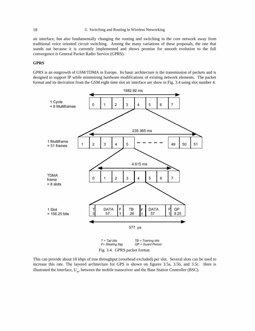
3. Switching and Routing in Wireless Networking18
air interface, but also fundamentally changing the routing and switching in the core network away fromtraditional voice oriented circuit switching. Among the many variations of these proposals, the one thatstands out because it is currently implemented and shows promise for smooth evolution to the fullconvergence is General Packet Radio Service (GPRS).
GPRS
GPRS is an outgrowth of GSM/TDMA in Europe. Its basic architecture is the transmission of packets and isdesigned to support IP while minimizing hardware modifications of existing network elements. The packetformat and its derivation from the GSM eight time slot air interface are show in Fig. 3.4 using slot number 4.
Fig. 3.4. GPRS packet format.
This can provide about 18 kbps of true throughput (overhead excluded) per slot. Several slots can be used toincrease this rate. The layered architecture for GPS is shown on figures 3.5a, 3.5b, and 3.5c. Here isillustrated the interface, Um, between the mobile transceiver and the Base Station Controller (BSC).

Raymond L. Pickholtz 19
BSC - SGSN
SNDCP
SNDCP
LLC LLC
RLC RLC
MAC MAC
Mobile
Um Network
Ph. Link
and RF
Ph. Link
and RF
Ref: GSM 03.60 series
SNDCP: Subnetwork dependence Convergence Protocol LLC: Logical Link ControlRLC: Radio Link LayerMAC: Medium Access Control
Fig. 3.5a. GPRS architecture.
Fig. 3.5b. GPRS network. Fig. 3.5c. GPRS routing.

3. Switching and Routing in Wireless Networking20
Once the packets get to this point, they can be switched and routed by any kind of packet switching networksuch as the Internet. The next step in the evolution of GPRS is Enhanced GPRS (EGPRS). This providesfor a higher radio interface rate and more flexible user rates. Enhanced Data Rates for Global Evolution(EDGE) will be introduced to boost network capacity and increase the data rates of both circuit switchingusing High Speed Circuit Switched Data (HSCSD) and packet switching (GPRS) up to three fold. Possiblerates may then exceed 400 kbps. The evolution of GPRS is believed by many to be the migration pathtowards a Universal Mobile Telecommunication System (UMTS) and the UMTS Radio Access Network(UTRAN)
Wireless ATM
An alternative contender for providing integrated wireless access and core network switching and routing isAsynchronous Transfer Mode (ATM) or perhaps more properly called “cell switching.” Originallydeveloped for wireline multimedia services, ATM has connection oriented features and the ability fordifferentiated services and negotiated bandwidth plus Quality of Service (QoS) guarantees, that has much torecommend it. One can build an entire end to end network based on ATM. Wireless ATM has become acandidate architecture that assumes that multimedia service will be ATM based. Figure 3.6 illustrates thebasic architecture. In this structure, developed by NEC Research, the air interface is ATM cells and a specialATM access point is provided to serve each geographical microcell. A new Mobile Network to NetworkInterface (M-UNI/UNI) is added. The User to Network (UNI) is standard. If IP networking is required thenthe proposal suggests carrying IP packets over ATM (IP/ATM).
AT M SWIT CH+ Mobility Ext
WAT M T ERMINAL
AT M ACCESS POINT
WATM RadioAir Interface
Mobile ATM“M” UNI/NNI
AT M HOST /SERVER
Standard UNI:ATM or IP/ATM
Standard UNI (+M):ATM or IP/ATM
WAT M cellsAT M cells
Radio Microcell 1
Radio Microcell 2
Fig. 3.6. Network architecture: Wireless ATM system.
Shortcomings
Wireless ATM appears to have some serious shortcomings. For example, since Adaptation Layer 2 (AAL2)appears to be the ideal mode to support both the radio interface and the core switching network, the use ofminicell packets (up to 42 octets) within AAL2 requires specific overhead for signaling and switching, theresult is a significant loss in efficiency. In addition, for high mobility users the Wireless ATM scheme maynot be easily scalable.
GPRS has its own problems in that it is a gradual approach to achieving the convergence objectives and inthe initial stages it is still tied to 2nd generation wireless techniques for roaming and mobility. Furthermore,once the packet gets into the TCP/IP network, it is not distinguished from non-wireless traffic. Radiotransmission is notorious for its many impairments such as fading, multipath, shadowing, and blockingwhich causes packets to be dropped or corrupted. The existing TCP protocols interpret this as congestionand take action that can severely reduce performance. In addition, TCP/IP is a connectionless service withno QoS guarantees and until new differentiated service features are introduced, a completely satisfactory

Raymond L. Pickholtz 21
solution is not possible. Other problems exist in the interaction of the higher layers of the protocol stackbecause of the anomalies of the physical layer that exists in wireless, and especially in high mobility andhandoffs.
Possibilities for Research
A possibly fruitful area of research for switching and routing in wireless networks is packet radio taken to itslimits. Packet radio per se has been investigated for many years as an application in military tacticalcommunications.
The ultimate solution may be to design the wireless network with an advanced version of packet radio moresuitable for the global commercial market. The large geographic coverage requires some form of cellularstructure where the mobiles act as relays to a cell site (or satellite) for long haul. In addition, the structure ofthe network is very “fluid” so that “ad-hoc” networks may be established without prior configuration. Thereis considerable research already underway for small scale ad-hoc wireless networks but that needs to beextended.
There is also a need for understanding the interaction of the higher layers of the protocol stack when they arebeing serviced by an unreliable and quirky wireless physical layer and the need for handoffs, mobility, androaming. A further positive note for direct wireless packet networks is that there are new protocol suitessuch as Ipv6, which have a very large address space, built in security features and characteristics thatincrease efficiency and performance. Another new direction in Internet development is Multiprotocol LabelSwitching (MPLS), which bears directly on the issues of the ability to independently route and switch manyconnections destined for the same address and allows a unique ability to optimize traffic flows and toemulate connection-oriented virtual circuit switching. MPLS has been advanced by the Internet EngineeringTask Force (IETF). It is a label switching technique that integrates layer 2 switching with level 3 routing.Label switched routers can improve performance and provide for differentiated services and multipleprotocols, including Ipv4 and Ipv6, among others. Although these ideas are being developed primarily withthe wired network, they have many potential benefits for the new multimedia broadband wireless systems.
CONCLUDING REMARKS
In the area of networking, switching and routing there will continue to be a disconnect between European,Japanese, North American, and worldwide standards.
Even through the 3rd generation, the interfaces, signaling, and roaming will remain incompatible.Furthermore, although there is every intention of providing higher data rates as well as voice telephony,many systems are unable to integrate voice, data, and multimedia so that there is a smooth convergence ofwireline and wireless networks. The third generation migration of GSM includes GPRS, which is apacketized transfer to the user level, but it is still based on connection oriented sessions by stealing slotsfrom the GSM TDM air interface. GPRS II extends the way that databases are accessed (for roaming, etc.)but the basic architecture is the same. In the United States, there are similar methods for AMPS CellularDigital Packet Data (CDPD), the North American TDMA IS 136 standard, as well as Packetcommunications in CDMA 2000. While there are many proposals to integrate ISDN, or ATM into thewireless network, there remain fundamental problems with them.
Incorporating the ability to use IP for mobile traffic is fraught with problematic issues ranging from effectsduring handoffs to roaming. Mobile IP as taken up by the IETF may be more suitable for relocation ofcomputer resources than to true mobility as in rapidly moving vehicles.
It appears that one way to achieve a true four-way convergence of wireline, wireless, telephony, andmultimedia traffic is to rethink the entire concept of leaving the core network as well as the air interface as aconnection oriented circuit switched network.

3. Switching and Routing in Wireless Networking22
Among the topics of needed research are the following:
• a scalable architecture that takes into account the wireless access model
• seamless operation across radio access fixed and core network
• simplified mobility procedures
• distributed databases for user services
• new ideas of the use of intelligent network (IN) concepts applied to new services including mobilewireless
• a multi-tier structure that will allow expansion of scale and new services not yet defined
ACKNOWLEDGMENT
This author had the benefit of discussions with many people and, in particular, would like to thank Dr. BijanJabbari of George Mason University for certain insights and Professor John Daigle and his student, VikanteChitre of the University of Mississippi, for permission to use Figures 3.4 and 3.5 on GPRS.

23
CHAPTER 4
CHANNEL CHARACTERIZATION AND PROPAGATION MODELS FOR
WIRELESS COMMUNICATION SYSTEMS
Magdy F. Iskander
INTRODUCTION
A wide variety of radio propagation models for different wireless services that specifically address varyingpropagation environments and operating frequency bands are generally known (Pahlavan et al. 1995; Jakes1974). A large number of propagation prediction models have been developed for various terrainirregularities, tunnels, urban streets and buildings, earth curvature, etc. (E. Vehicular Technology Society1988; Lee 1989; Parsons et al. 1998). For propagation models addressing satellite communications systems,on the other hand, different types of issues including rain attenuation and atmospheric effects are routinelyconsidered (Dissanayake et al. 1997). The level of sophistication in the development of these models alsodepends on the longevity of the related technology. For example, the importance of developing propagationmodels suitable for satellite communications, and in particular the development of reliable models for rainattenuation and other atmospheric impairments along earth-satellite paths, has long been recognized; andextensive research activities have been focused on addressing these effects (Capsoni et al. 1987; Stutzman1995). With the development of new satellite services incorporating very small aperture terminals (VSAT)and ultra small aperture terminals (USAT) in the Ka-band (20-30 GHz) frequencies, more recent researchefforts in this area have focused on refining available propagation models to account for and accuratelypredict the total propagation link margin that includes other propagation impairments such as cloudattenuation, gaseous absorption, and low-angle fading. European and U.S. agencies are compiling severaldatabases that should enable the evaluation of propagation models that attempt to combine differentpropagation effects (Dissanayake 1997). These research activities and available results should also be usefulin addressing the needs of new emerging high frequency and point to multi-point terrestrial wirelesscommunication systems such as the local multi-point and point-to-point distribution systems (LMDS andPPDS, respectively) and wireless local area networks.
With the phenomenal growth in mobile and portable terrestrial wireless communication systems, and due totheir potential utilization in a wide variety of high data rate and multimedia services, higher frequency bandsneed to be allocated and utilized for these services. New devices and components for high frequency andmillimeter wave integrated front-end receivers are being developed, active and low cost phased arrayantennas are being designed, and advanced software issues in coding, modulation, switching, andnetworking are being researched and developed. In addition to these rather obvious advances that areneeded to enable the next generation wireless technology, developing new and more computationallyefficient propagation models is also essential. Development of reliable propagation models and theavailability of the associated simulation software tools would be absolutely necessary for the successfulimplementation of the future terrestrial wireless systems and also for their integration with other technologies

4. Channel Characterization and Propagation Models for Wireless Communication Systems24
including the satellite, LMDS, and the wireline based services. Accurate propagation models will help inusing the rather congested frequency spectrum more efficiently, in planning more effective radio networks,and in implementing cost effective solutions for a desirable and user specific communication coveragepattern.
PROPAGATION MODELS FOR URBAN ENVIRONMENT
For urban propagation, three distinct models can be used. These include propagation in macrocells,microcells, and indoor or picocells. In macrocells, the base station is often placed well above an averagerooftop, while for microcells the base station is placed well below the average rooftop. In macrocells, thepropagation path is dominated by the over the rooftop path, while for microcells reflections and diffractionfrom buildings and streets often dominate the propagation environment. For such environments, ray tracing-type simulation models are adequate and their use is justifiable. For picocells and indoor propagation, on theother hand, new challenges appear and improved propagation models and simulation tools are required toachieve reliable, accurate, and computationally efficient propagation predictions and to help overcome manyof the indoor propagation impairments. Challenges facing the development of picocell simulation tools mayinclude the following:
• Propagation predictions depend primarily on often unavailable building construction parameters such aswall thickness, materials, and indoor building structures.
• Exclusive use of ray tracing-based propagation models may be inadequate. Available ray tracingprocedures often encounter a large number of reflections and multiple transmissions and hence becometime consuming and computationally inefficient.
• Lack of knowledge of diffraction coefficients for many indoor structures may also compromise theaccuracy of available ray tracing simulation methods.
• The ray tracing procedure and the geometrical theory of diffraction are high frequency techniques, anddimensions of some of the indoor structures may not necessarily satisfy the small dimensions comparedto the wavelength criterion required by these methods.
It is often argued that results from deterministic electromagnetic-based calculation models are not expressedin terms of parameters that can be used in the simulation of wireless communications systems. Parameterssuch as delay spread, coverage, direction of arrival, and bit error rate (BER) are necessary for systemsimulations and need to be incorporated as part of the simulation code development.
Four different types of methods are often used in developing propagation models, and the above listedlimitations are expected to impact them differently. For example, statistical models provide parameterssuitable for system simulations but lack specificity and accuracy. EM-based deterministic models, on theother hand, provide accurate and site specific coverage and delay spread information but are also verycomputationally inefficient and time consuming. Empirical and measurement-based models are site specific,frequency specific, and hence lack generality. Researchers use a combination of these methods to helpimprove the accuracy, broaden the generality, and reduce the required computational time. But much moreresearch and development are needed to fully develop accurate, computationally efficient, andexperimentally verified propagation models that may be used for broadband and highly mobilecommunications systems. With the advances in the signal processing methods and the development ofcommunications algorithms, the envisioned propagation models are expected to play a critical role in theaccurate accounting for mobility and the dynamic variation in the characteristics of the propagation channels.
With this in mind, the panel members tried to identify and possibly discuss the on-going R&D activities inthis area of channel characterization and propagation models as we continued to travel in Europe and Japan.Only at Philips, CSELT, and Ericsson in Europe, and Matsushita Research Institute Tokyo (MRIT), KDD,and YRP in Japan did the panel identify research activities that the host was interested in sharing anddiscussing. The following provides a summary of these activities and a comparative study of the level of

Magdy F. Iskander 25
interest and the type of emphasis in each case. This summary will be presented according to the modelingand the characterization technique used in research activities at the visited sites.
Deterministic EM-Based Propagation Models
The WTEC panel identified strong research activities in this area at Philips and Ericsson. At Philips, newdeterministic models for indoor propagation are being developed based on modal expansion techniques andusing the Finite Difference Time Domain Method (FDTD). In both cases, both the EM field distributionsand statistical parameters such as coverage and delay spread were being calculated (Dolmans 1997).Examples of the obtained results using a 2D FDTD code are shown in Fig. 4.1 for two different indoorpropagation environments. Results from some of the statistical parameters calculations are shown in Fig. 4.2where both the delay spread profile for propagating pulses of different widths and the coverage for singleand diversity antennas were calculated. Results from these calculations are being experimentally evaluatedusing experimental set ups such as the one shown in Fig. 4.3. The important observation from this effort isrelated to the fact that efforts are being made to include calculations of statistical parameters of interest tosystem simulations and to verify the results experimentally. The use of 2D FDTD calculations emphasizethe need for a more computationally efficient procedure to carry out 3D calculations often required in indoorsimulations.
The research activities at Ericsson are closely tied with the European Cooperation in the Scientific andTechnical Research (COST) in this area.
The COST 295 task force on “Wireless Flexible Personalized Communications” has a working group(Working Group 2) on propagation and antennas. This working group, chaired by Prof. E. Bonek from theTechnical University of Vienna, has the following stated objectives:
• develop new EM-based deterministic models for UHF, microwave, and millimeter wave
• study and optimize models for short range communications
• conduct a comparative study of the effectiveness of empirical/statistical and electromagneticdeterministic models for different propagation environments and situations
• conduct measurements to validate accuracy and improve efficiency
As part of this activity, Mr. M. Steinbaur, also from the Technical University of Vienna, is leading an effortto provide characterization for wideband and time-varying directional channels and to ensure that modelsmeet requirements posed by system and network simulations. A summary of the progress and discussion ofactivities of the COST 295 task force, working group 2, is available elsewhere (COST 295/260 Workshop1999; Landstorfer 1999).
(a) (b)
Fig. 4.1. Fluctuations of the electric field in the building that houses the faculty of Electrical Engineering.2D FDTD code was used in these calculations which include the following: (a) all doors are openwith no object present; (b) doors are closed with one object placed in one of the rooms. Greencolor denotes high electric field values; blue color represents low signal amplitudes.

4. Channel Characterization and Propagation Models for Wireless Communication Systems26
Ex
[V/m
]
t [ ]µs t [ ]µsDelay profile of the electric field Ex
(a) (b)Fig. 4.2. Coverage distribution in an indoor environment using space diversity receivers (a) 0-100%,
(b) 98-100. The diversity combining consists of a switch (dashed-dotted), a selectionreceiver (short dashes), an equal-gain combiner (dotted), a maximum-ratio combine (longdashes). The coverage for a single antenna receiver is represented by the solid curve.
Schematic diagram of the measurement set-up
Photograph of the measurement setup for a prototype of an adaptive DECT handset
Fig. 4.3. A photograph and schematic diagram of the adaptive/diversity antenna measurement system(W.M.C. Dolmans, Eindhoven University of Technology/Philips Research Laboratory).
Ray Tracing-Based Propagation Models
The ray tracing method represents the most commonly used approach in the calculation of propagationmodels for terrestrial and urban environments. Several software packages are available (Bertoni et al. 1994;Liang et al. 1998; Rappaport et al. 1992), and some research efforts are underway to help in the continuedimprovement of the accuracy and extension of generality and to increase computational efficiency. Theconventional ray tracing method is based on a ray launching and bouncing procedure that can be veryinefficient if no speed-up algorithm is employed. There have been several schemes to accelerate thisprocedure including the image method, the bounding box method, and the utilization of the visibility

Magdy F. Iskander 27
approach (Landstorfer 1999; Liang et al. 1998; Catedra et al. 1998). Although these methods have their ownadvantages and specific domains of applications, more efficient methods are needed to cope with thecomplex and often computationally demanding indoor or indoor/outdoor situations while maintaining goodaccuracy of the propagation prediction results. Such research activities were found at CSELT in Italy andKDD Research and Development Laboratories in Japan. At CSELT results from several models werepresented including site specific ray tracing predictions which were time consuming; ray-launching results,which were faster but lacked accuracy; and semi-deterministic methods, which were being used in small cellplanning. For indoor propagation, however, empirical models based on experimental measurements werebeing used. Results from these calculations were presented in terms of field distributions in the propagatingenvironment, delay spread distribution, and Doppler frequency distribution. An example of the presentedresults for a microcellular structure is shown in Fig. 4.4.
Fig. 4.4. Microcell structure (L.) and ray tracing results (R.) of delay profile in a parking lot (CSELT).
At KDD two tools were developed. These include the CSPLAN tool, which is used for cell site planning andcoverage evaluation using low antenna height and 2D building shapes, and the BSPLA tool, which providespropagation predictions for mobile based station planning. For the BSPLA tool, path loss is evaluated basedon geographic information of the propagation area. This effort at KDD points to other ongoing researchactivities in the area of channel characterization and propagation models development, including the use ofgeographic information and data from the Global Positioning System (GPS) to guide the development andenhance the accuracy and the computational efficiency of new propagation models for future wirelesscommunications systems (Enge 1994; Kaplan 1996). This may provide significant advantages in systemsthat intend to incorporate dynamic variations in channel characteristics. For mobile multimedia wirelessapplications, incorporation of such capabilities may be crucial in enhancing the quality of service or makingit even possible in the first place.
Propagation Models At Millimeter Waves
Besides the stated objective by the COST 295 working group, the issue of developing propagation models atmillimeter wave frequencies was not discussed in any of the visited European sites. Two groups in Japan,however, discussed R&D activities in this area. These include the MRIT and the Stratospheric WirelessAccess Network group at the Yokusuka Research Park (YRP). At MRIT new propagation models are beingdeveloped at millimeter wave frequencies, and emphasis is placed on the accurate accounting of multi-pathanalysis. At YRP, on the other hand, propagation models are being developed to support the development ofa stratospheric platform. This unmanned High Altitude Platform Station (HAPS) is expected to fly at analtitude of 22 km, and 15 platforms are expected to provide coverage for all of Japan. Frequencies in therange from 2-20 GHz will be used with the continued increase in attainable data rates. Figure 4.5 shows thatoptical links will be used for inter-platform communications and radio links will be used for subscriber
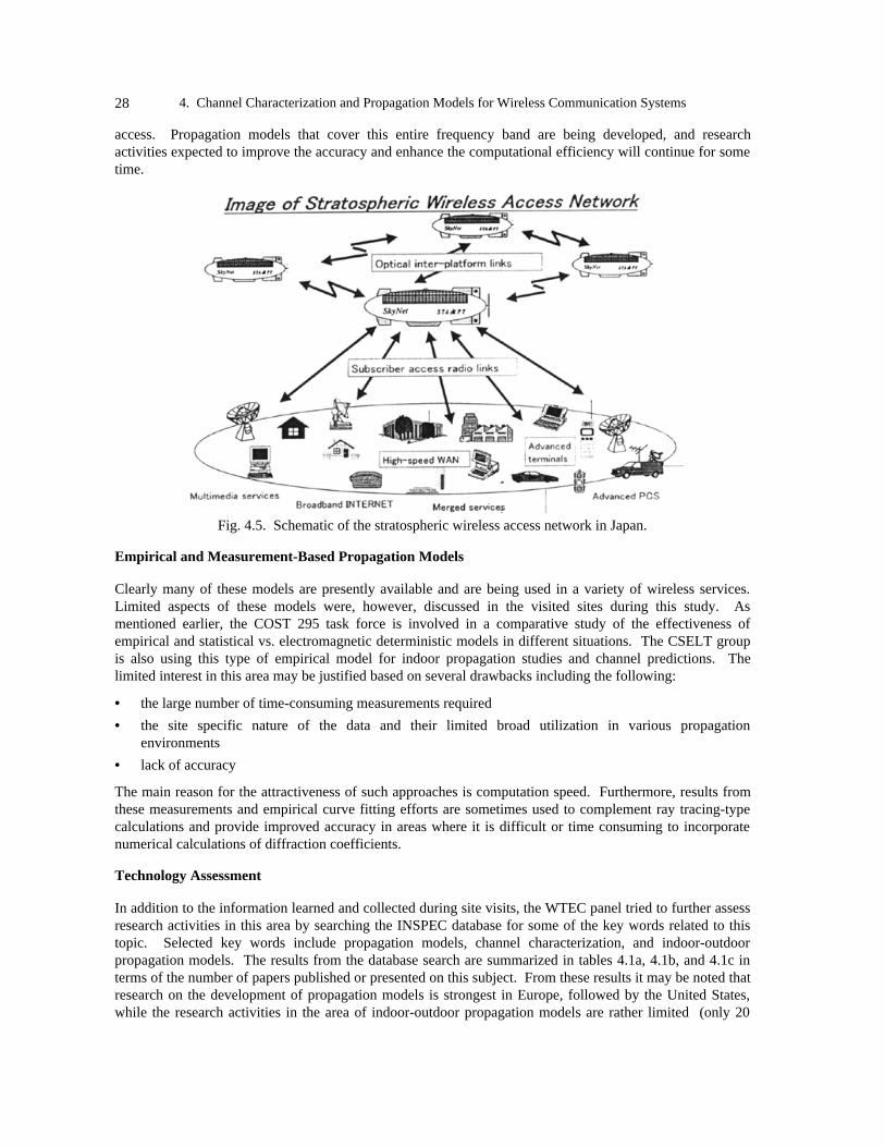
4. Channel Characterization and Propagation Models for Wireless Communication Systems28
access. Propagation models that cover this entire frequency band are being developed, and researchactivities expected to improve the accuracy and enhance the computational efficiency will continue for sometime.
Fig. 4.5. Schematic of the stratospheric wireless access network in Japan.
Empirical and Measurement-Based Propagation Models
Clearly many of these models are presently available and are being used in a variety of wireless services.Limited aspects of these models were, however, discussed in the visited sites during this study. Asmentioned earlier, the COST 295 task force is involved in a comparative study of the effectiveness ofempirical and statistical vs. electromagnetic deterministic models in different situations. The CSELT groupis also using this type of empirical model for indoor propagation studies and channel predictions. Thelimited interest in this area may be justified based on several drawbacks including the following:
• the large number of time-consuming measurements required
• the site specific nature of the data and their limited broad utilization in various propagationenvironments
• lack of accuracy
The main reason for the attractiveness of such approaches is computation speed. Furthermore, results fromthese measurements and empirical curve fitting efforts are sometimes used to complement ray tracing-typecalculations and provide improved accuracy in areas where it is difficult or time consuming to incorporatenumerical calculations of diffraction coefficients.
Technology Assessment
In addition to the information learned and collected during site visits, the WTEC panel tried to further assessresearch activities in this area by searching the INSPEC database for some of the key words related to thistopic. Selected key words include propagation models, channel characterization, and indoor-outdoorpropagation models. The results from the database search are summarized in tables 4.1a, 4.1b, and 4.1c interms of the number of papers published or presented on this subject. From these results it may be noted thatresearch on the development of propagation models is strongest in Europe, followed by the United States,while the research activities in the area of indoor-outdoor propagation models are rather limited (only 20

Magdy F. Iskander 29
papers cited during the period from 1995-99) with major participation by the European community. Theseresults also emphasize the need for new R&D for modeling micro- and pico-cells.
Table 4.1aPropagation Models (1998-1999)*
U.S.A. 21 21%
Europe 38 38%
Japan 8 8%
Canada 6 6%
Others 27 27%
*Results of the database search using INSPEC. Total number of papers, 100.
Table 4.1bChannel Characterization (1997-1999)*
U.S.A. 16 38%
Europe 19 45%
Japan 1 2.4%
Canada 2 4.8%
Others 4 9.5%
*total number of papers 42
Table 4.1cIndoor-Outdoor Propagation (1995-1999)*
U.S.A. 3 15%
Europe 9 45%
Japan 1 5%
Canada 2 10%
Others 5 25%
*total number of papers 20
For the overall comparative study among Europe, Japan, and United States in the area of channelcharacterization and modeling, Table 4.2 was prepared to provide a qualitative comparison. From Table 4.2it may be noted that while the majority of the available models are based on the computationally efficientstatistical and empirical models, there is some growing interest in using EM-based deterministic modelsparticularly in the United States followed by Europe. Efforts to integrate statistical parameters in the modelsare being mostly emphasized in Europe followed by the United States. It is expected that this trend willcontinue to grow because of the continued demand for improved accuracy and reliability in system designsand network planning. Table 4.2 also shows some growing interest in modeling new wirelesscommunications systems in the millimeter wave frequency range in both Japan and the United States, whilemuch of the European activity is presently focused on addressing the present industrial needs at lower RFfrequencies.

4. Channel Characterization and Propagation Models for Wireless Communication Systems30
Table 4.2Research Activities in the Channel Characterization and
Propagation Models in Europe, Japan and the United States
Europe Japan USA
Statistical/empirical *** *** ***
EM based deterministic ** * ***
Integrative models(Statistical parameters based on deterministic models)
** - *
Microwave and millimeter wave * ** **
*Qualitative results of a comparative study illustrating the level of activities and the focus of research in Europe, Japan,and the United States in the area of channel characterization and propagation models.
KEY RESEARCH ISSUES
From the preceding discussion and keeping in mind the stated vision for next generation wireless technologyof fully integrated, reliable, multimedia services with full mobility and minimum latency, the following keyresearch activities in the channel characterization and propagation model development may be suggested:
• new models for microwave and millimeter wave wireless systems
• models for broadband wireless systems including polarization diversity and mobility effects
• computationally efficient deterministic/quasi-deterministic models that maintain good accuracy andgenerality of application
• integrated models that provide statistical parameters relevant to system and network simulations
• experimental measurements on scaled models or realistic channels to validate simulation results andprovide guidance for identifying the most important contributions to propagation impairments andinterference effects
While emphasis in this chapter was placed on channel characterization and propagation models, it isimportant to point out that multidisciplinary efforts that incorporate knowledge of the channel characteristicsto develop and implement novel signal processing methods, communication algorithms, and networkingprotocols represent a most effective strategy in advancing wireless communications systems. Every effortshould be made to participate in these integrative and multidisciplinary approaches rather than focusing onisolated and individual efforts in channel characterization and modeling.
In addition to the need for integrative efforts, there is no question that research efforts must focus on thedevelopment of a physics-based channel model that effectively takes advantage of the identified dominanteffects in a given propagation environment and frequency band while maintaining good accuracy. A broadrange of applicability and acceptable computational efficiency will provide next generation wirelesscommunications systems with a significant tool and a most valuable enabling technology. Understanding thephysical nature of the wireless communication channel and incorporating this developed fundamentalunderstanding across the communications layers is crucial for realizing the much anticipated benefits fromthe wireless information technology and networks.
REFERENCES
Bertoni, H.L., W. Honcharenko, L. R. Maciel, and H. H. Xia. 1994. “UHF propagation prediction for wireless personalcommunications.” Proceedings of IEEE 82:1333-1359.
Capsoni, C., F. Fedi, and A. Paraboni. 1987. “A comprehensive meteorologically oriented methodology for theprediction of wave propagation parameters in telecommunication applications beyond 10 GHz.” Radio Science22:387-393.

Magdy F. Iskander 31
Catedra, M.F., J. Perez, de Adana, and Gutierrez. 1998. “Efficient ray-tracing technique for 3D analyses of propagationin mobile communications: application to picocells and microcell scenarios.” IEEE Antennas and Propagation. 40(2):15-28.
Dissanayake, A., J. Allnutt, and F. Haidara. 1997. “A prediction model that combines rain attenuation and otherpropagation impairments along Earth-satellite paths.” IEEE Trans. Antennas and Propagation 45 (10):1546-1557.
Dolmans, W.M.C. 1997. “Effect of indoor fading on the performance of adaptive antenna system.” Ph.D. dissertation,Department of Electrical Engineering, Eindhoven University of Technology, Eindhoven, The Netherlands.
E Vehicular Technology Society. 1988. “Special issue on mobile radio propagation.” IEEE Tran. Veh. Technol. 37:3-72.
Enge, P.K. 1994. “Global positioning systems: signals, measurements, and performance.” International J. WirelessInformation Networks 1(2).
Jakes, C., ed.. 1974. Microwave Mobile Communications. New York: John Wiley & Sons.
Kaplan, E.D., ed. 1996. Understanding GPS: Principles and Applications Boston: Artech House.
Landstorfer, F. 1999. “Wave propagation models for the panning of mobile communication networks.” Plenarypresentation read at European Microwave Conference, 4-8 October, Munich, Germany.
Lee, Y. 1989. Mobile Cellular Telecommunications Systems. New York: McGraw-Hill.
Liang, G. and H. L. Bertoni. 1998. “A new approach to 3-D ray tracing for propagation prediction in cities,” IEEETrans. Antennas and Propagation 46:853-863.
Pahlavan and A.H. Levesque. 1995. Wireless Information Networks. New York: John Wiley & Sons.
Parsons, J.D. and J.G. Gardiner. 1998. Mobile Communication Systems. Glasgow: Blackie.
Proceedings of COST295/260 Joint Workshop. 1999. “Spatial Channel Models and Adaptive Antennas.” April 20-21,Vienna, Austria.
Rappaport, T.S. and D.A. Hawbaker. 1992. “A ray tracing technique to predict path loss and delay spread insidebuildings.” Proc. IEEE GLOBCOM’92 Dec: 649-653.
Stutzman, W.L., T. Pratt, A. Safaai-Jazi, P.W. Remaklus, J. Laster, B. Nelson, and H. Ajaz. 1995. “Results fromVirginia Tech propagation experiment using the Olympus Satellite 12, 20, and 30 GHz Beacons.” IEEE Trans.Antennas and Propagation 43 (Jan): 54-62.

4. Channel Characterization and Propagation Models for Wireless Communication Systems32

33
CHAPTER 5
HARDWARE FOR RF FRONT-END OF WIRELESS COMMUNICATION
Tatsuo Itoh, Linda Katehi
INTRODUCTION
Hardware provides the building blocks for the specified requirements and functions of wirelesscommunication systems. In many defense and satellite systems, devices and circuit designs are aimed at thebest performance, although the choice of hardware is often conservative. In the case of wirelesscommunication systems, this conservative approach is somewhat true because of the rapid turnaround incommercial products. In fact, manufacturability and marketability become the drivers for many high volumeshort-cycle commercial products as many industrial participants in this study like Dr. J. Golio of Rockwellemphasized. However, in looking at the future beyond the G3 and even G4 environment, researchconcerning hardware needs to be advanced in a steady and accelerated pace. This includes not only devicesand circuits, but also enabling process technology and design methodologies. This is because theperformance of future wireless systems critically depends on hardware capability. Dr. Golio mentioned thatthe faster, smaller, lighter and cheaper philosophy still holds. It is also true that research methodologies forhardware may need to be modified.
One of the factors influencing hardware research is the frequency of operation, which affects bandwidth andsignal processing speed. Although much industrial effort is aiming at frequencies up to 2.4 GHz (at most 5.7GHz) for mobile wireless and 28 GHz for fixed wireless such as LMDS, several industrial research centersare looking at much higher frequencies beyond 60 GHz. Although the need for bandwidth far exceeding theG3 requirement is often questioned, research on higher frequency devices and circuits has at least twobenefits. One is to enable a potential system that takes advantage of the wider bandwidth such as 5 GHzaround a carrier frequency of 60 GHz, as envisioned by Sony for ultra-wideband wireless connections.Another is to make low frequency design more flexible and device and circuit performance superior throughthe availability of higher frequency devices used lightly.
Since hardware research is motivated by system requirements, listing some of the desired features for thefuture systems and the potential technologies necessary to achieve these goals is a good place to begin. Thelist is not intended to be exhaustive, but it includes features envisioned by some industrial participants in theWTEC study. Dr. Walid Ali-Ahmad of Maxim, who is engaged primarily in silicon based wireless systems,provided the following list of targets for future circuits and devices:
• complete wireless system on chip including radio frequency (RF), analog baseband, digital baseband,digital logic, digital signal processing (DSP), microprocessor and power supply1
1 At the recent Workshop on Single Chip Radio during the 1999 IEEE International Microwave Symposium, mostpanelists expressed the desirability (but extreme difficulty) in achieving this in the foreseeable future.

5. Hardware for RF Front-End of Wireless Communication34
• low cost system solution with minimum off-chip component count, high yield process
• small size system solution and portability
• very low power consumption and extended battery life
Dr. Ali-Ahmad provided the following list of device and circuit technologies needed:
• MEMS devices and micromachined components including the high-Q on-chip filters
• advanced IF circuits for software radio
• advanced process technology
• optimized RF silicon transistors for high efficiency linear power amplifiers
• continued scaling of complementary metal oxide semiconductor (CMOS) technology
• advanced packaging
• battery technology
• CAD for system-on-chip design
In regard to the device technology, a number of other study participants from the United States and abroademphasized the importance of III-V devices for high frequency applications such as 5.7 and 60 GHz (Mr.Kawasaki of Sony, Dr. K. Honjo of NEC, Dr. Kagiwada of TRW). In fact, TRW can deliver a 190 GHzamplifier based on III-V technology. On the other hand, many people considered SiGe as a promisingdevice with potential low cost, high frequency applications.
CMOS TECHNOLOGIES AND SILICON BIPOLAR TRANSISTORS
CMOS and silicon bipolar devices and circuits currently are responsible for the majority of wirelesscommunication hardware. Silicon technology has a long history for digital signal processing, VLSI, A/Dand D/A converters. CMOS based radio has been steadily progressing toward higher frequencies. State-of-the-art CMOS uses the 0.18 µm process. CMOS is currently the workhorse for wireless up to 800 MHz.Substantial effort is being expended worldwide to extend the frequency to 1.9 GHz, 2.5 GHz and 5 GHzranges. One of the major drawbacks for silicon devices used for RF applications is the low resistivity ofsilicon, causing substrate loss. This problem causes low Q of passive circuits, particularly for inductors.Much effort is spent to enhance the capability of silicon circuits by, e.g., elevating the inductor from the chipto increase Q and by introducing SOI (silicon on insulator) technology for power and speed.
Philips Research Laboratories have been working on “silicon-on-anything” devices based on the bipolarprocess with the circuits transferred to a range of insulating substrates such as glass (Fig. 5.1). In this waythe parasitic capacitance is reduced, and high-quality RF passive components can be integrated on the chip.They have manufactured RF devices, including a bipolar transistor with an active emitter of only 0.05 squaremicrometers and with proportionately smaller junction capacitances. This resulted in low powerconsumption with only 15 µA at the cut-off frequency of 10 GHz. One example of the chips is a fullyintegrated LC-type VCO including a phase-locked-loop frequency synthesizer and divider chain for localarea networks (LANs).
Much effort has been expended to improve performance by changing the device fabrication process. Forexample, Philips has proposed a double-poly-transistor with SiGe in-situ grown base (Fig. 5.2). Thetraditional base contacts are eliminated. Instead, the base contacts are poly-silicon strips on a thick oxidelayer. The base layer is grown into the narrow opening in the oxide and automatically contacts the poly-silicon strips. Finally, heavily n-doped poly-silicon is deposited to form the emitter. Adding 10 to 20% Geto the base layer offers new possibilities to adjust device parameters.

Tatsuo Itoh, Linda Katehi 35
Fig. 5.1. An example of a silicon-on-anything circuit by Philips Research Laboratory.
Fig. 5.2. Double-poly transistor by Philips Research Laboratory.
Although it has not used CMOS, NEC has utilized Si nMOSFETs (field-effect transistors) for both a lowfrequency (900 MHz) amplifier for GSM and high frequency (Ku band) amplifier (Fig. 5.3). Since thesubstrate is lossy, the amplifier design for 900 MHz makes use of the loss matching technique to obtain anunconditional stability from a conditionally stable design to obtain a power added efficiency (PAE) of 62%with the power output Pout of 27 dBm. The device uses two-generation old 0.6 µm technology. For the Kuband amplifier based on 0.18 µm nMOS (with fT of 50 GHz and fmax of 45 GHz), the substrate loss is toosignificant to use the same approach. Therefore, the transmission line structures for the circuit are modified(Fig. 5.4). For “Type A” modification, microstrip lines are placed on a polyimide layer that is in turn placedon Si substrate via SiO2 and SiON isolation layer. In “Type B,” a thin-film microstrip line that has an Allayer inserted in the SiON and SiO2 layers is used. The insertion loss is about 1 dB/cm. The amplifier gainis 10 dB with a noise figure of 4 ~ 5 dB in Ku band.
One technology that has drawn recent attention is SOI (silicon on insulator). Recently IBM announced thatit plans to use SOI technology to manufacture a range of logic integrated circuits (ICs). IBM’s first0.22 micron SOI devices were scheduled to be used in Apple Computer Inc.’s Macintosh systems and inIBM servers, perhaps by early in the year 2000. IBM is also developing 0.18 and 0.13 micron processes for1 GHz microprocessors. Along with up to 30 percent performance gains, SOI could improve powerconsumption by 30 to 50 percent. Because SOI’s advantage is more pronounced at low-voltage operation,the technology is suitable for mobile applications, with reasonable RF performance at single-volt supplyvoltages well above a few GHz. Similarly, Motorola is preparing an SOI BiCMOS process for RF/IFcircuits for cellular phone applications.

5. Hardware for RF Front-End of Wireless Communication36
Fig. 5.3. nMOSFET characteristics by NEC.
Fig. 5.4. Transmission lines on an Si substrate used by NEC.
Many modern wireless communication systems use digitally modulated signals. Therefore, at some pointthis digital information needs to be extracted so that DSP can take over. Much work has been carried out forthe direct conversion receiver. Central to this scheme are AD and DA converters. Although there is a needto place this A to D conversion scheme as close to the antenna as possible, the performance of the AD andDA converters set the limit (Fig. 5.5). The bit rate and the frequency are in a trade-off relationship. Analogto digital conversion improves 1 bit/3 years according to Philips, and CMOS AD conversion may slow downdue to low VDD. In fact, a good rule of thumb to describe a figure-of-merit of the AD converter is given by
F = log2(Sampling Speed) + Resolution (given as Effective No. of bits)
For the state of the art, this F value ranges from 38 to 40 at the moment. For example, for 1 GHz speed with10 bits of resolution, F becomes 40.

Tatsuo Itoh, Linda Katehi 37
Fig. 5.5. Recent and projected trends for AD conversion for 1990-2002 (Philips).
III-V DEVICES AND CIRCUITS
Although the market is much smaller than that for silicon based devices, III-V devices have been developedfor high performance, high frequency applications from UHF to millimeter-wave frequencies. In addition tothe discrete devices, the past several years have seen significant advances in MMIC based on III-V materials.The most common baseline materials are GaAs and InP. GaAs metal Schottky FETs (MESFETs) are quitemature and are available off the shelf up to X and Ku band applications. More advanced high electronmobility transistor (HEMT) devices are the preferred choice for higher frequency and higher performanceapplications with lower noise figures for low noise amplifiers. InP HEMT provides better performance forhigher millimeter wave frequencies as demonstrated by Daimler-Chrysler in Fig. 5.6.
Fig. 5.6. Daimler-Chrysler InP-based HEMTs.
TRW recently demonstrated the world’s first 190 GHz InP HEMT low noise amplifier (LNA), whichexhibited a gain of more than 7 dB from 160 – 190 GHz, with a peak of 9.6 dB, while the noise figure is6 dB at 170 GHz (see Fig. 5.7). This device has a 70 nm e-beam defined T-gate on a 2-mil substrate with a25 µm backside via. TRW also has demonstrated an InP HEMT MMIC power amplifier with an outputpower of 427 mW with PAE of 19% and an associated gain of 8.2 dB (see Fig. 5.8). The state of the artdevices exhibit fT > 300 GHz and fmax > 500 GHz. The expected future performance would be fT > 500 GHz,fmax > 1 THz, and an LNA with a gain of 10 dB at 260 GHz, as well as a PA with an output power of 0.25 Wat 260 GHz.

5. Hardware for RF Front-End of Wireless Communication38
Fig. 5.7. TRW 190 GHz InP HEMT low noise amplifier.
Fig. 5.8. TRW W-band In-P HEMT power amplifier.
For applications at somewhat lower frequencies, GaAs HEMT (PHEMT or pseudomorphic HEMT) is a verypractical and readily available device. In fact, Dr. Honjo of NEC believes that wireless applications up to100 GHz do not require the use of InP devices. For future mobile wireless communications for multimedia,a high speed (> 20 GHz) and low power phase lock loop (PLL) is required. NEC has developed a CPW-based MMIC using a 0.1 µm GaAs E/D-HEMT. The salient feature of this device is the use of a two stagemushroom gate (see Fig. 5.9).

Tatsuo Itoh, Linda Katehi 39
Fig. 5.9. NEC two-stage mushroom gate HEMT.
A new type of microwave device that has drawn a considerable research attention is III-V heterojunctionbipolar transistor (HBT). This device tends to have a lower phase noise than FET type devices. At themoment, the usable frequency range is lower, however. NEC uses selective regrowth to reduce the baseresistance to one fourth (see Fig. 5.10). At the same time, pseudomorphic InGaAs graded base was used sothat the regrowth-performed GaAs-based HBT achieved low RbCbc leading to an fmax comparable to those ofhigh-performance InP-based HBT that has a higher fT. Some of their devices include (1) a 26 GHz poweramplifier module made of two device power combined with 3.63 W and PAE of 21%, (2) a 1W 35 GHzHBT power amplifier with PAE of 29% and a 60 GHz dynamic frequency divider, and (3) a low phase noise38 GHz HBT MMIC VCO.
Fig. 5.10. NEC high fmax HBT technology.
SiGe DEVICES AND CIRCUITS
To achieve high integration and multifunction capability, industry is pursuing the development of SiGe forrange sensors, speed control, etc. In addition to integration and performance, this technology is likely to beutilized in customer products for wireless applications including communications and sensing/navigation.Comparisons made between InP-, GaN- and SiGe-based products show superior cost potential in the SiGetechnology (see Fig. 5.11) and indicate device superiority due to very low 1/f noise and low phase noise.SiGe transit-time diodes in self-oscillating mixers have demonstrated frequency stability with subharmonic

5. Hardware for RF Front-End of Wireless Communication40
locking. Free running has demonstrated about -60 dBc/Hz at 100 kHz from the carrier, and with phaselocking about –90 dBc/Hz at 100 kHz from the carrier. In this circuit technology, CPW has been chosen asthe interconnect medium due to its superiority to thin film microstrip and its associated need of a via holetechnology. CPW solves a number of problems but requires an air-bridge technology, which in terms offabricating is easier to establish due to its requirements for wafer-surface and not wafer-bulk fabrication.Daimler-Chrysler is a leader in SiGe technology and has demonstrated performance records in SiGe HBT, asshown in Fig. 5.12. A number of SiGe applications include Ka-Band CPW oscillator HBTs, a 77 GHz near-field sensor with SiGe Schottky diodes, a 77 GHz closing velocity sensor, etc. While SiGe technology isprogressing fast, a number of processing issues still need to be resolved. To alleviate some of these issues,passivation of the device by Si3N4 has been adopted. Low temperature, low-power cpw-based HBTstructures are routinely demonstrated (20 mW at 47 GHz) (6 emitter figure device). Presently research isfocused on the development of phase resonant devices with fmax=300GHz achieved by quantum-wellinjection.
SiGe SIMMWIC: MotivationMaterial data and costs
Silizium GaAs
Good RF performance data of GaAs
Cost advantage (1 order of magnitude) of silicon !
PermittivityElectron mobilityBreakdown fieldThermal conductivityMechanical stabilitySubstrate cost
11,671500 cm2/Vs3 x 105 V/cm1,5 W/cmK
hoch< DM 10 - 6“ (low
resistivity)DM 30 - 4“ (high
resistivity)
12,78500 cm2/Vs4 x 105 V/cm0,46 W/cmK
geringDM 200 - 3“ (semi-
insulating)
Fig. 5.11. Comparison of GaAs and SiGe (Daimler-Chrysler).
Monolithical integratedcoplanar 6 finger HBT structure
1.5 2.0 2.5 3.0 3.5 4.0 4.5
-5
0
5
10
15
outp
ut p
ower
(dbm
)
collector-base voltage vcb
(V)
46.96
46.98
47.00
47.02
47.04
osc
illat
ion
freq
uenc
y (G
Hz)
47.0224 47.0226 47.0228 47.0230 47.0232 47.0234-80
-60
-40
-20
0
59.31 dBc
100 kHz Span: 1MHzVBW: 10 kHzRBW: 10 kHz
outp
ut p
ower
(dbm
)
frequency (GHz)Power density spectrum
-0.84 -0.82 -0.80 -0.78
6
8
10
12
14
outp
ut p
ower
(dbm
)
emitter-base voltage veb
(V)
46.96
46.98
47.00
47.02
47.04
osc
illat
ion
freq
uenc
y (G
Hz)
Performance - world-record !SiGe SIMMWIC: (Modules)
Power vs Collector voltage
Power vs Emitter voltage
Fig. 5.12. World record performance of SiGe HBTs (Daimler-Chrysler).
Daimler-Chrysler is inserting this technology into customer products via an extensive product developmenteffort performed in the “Microwave Factory” owned by DASA. Sensors have been produced such asSatCom, MobilCom, Cruise control at 77 GHz and LMDS at 28 GHz, in addition to 24 GHz radar designed

Tatsuo Itoh, Linda Katehi 41
to measure material properties for application in steel production. Other products include a 58 GHz point-to-point link in hybrid configuration with GaAs MMICs using bonding wires for connection to MMIC chips.
GaN DEVICES AND CIRCUITS
Devices based on a wide bandgap semiconductors also have received considerable attention. In particular,GaN based devices are considered more appropriate for higher frequency operations than SiC based ones.Although GaN has been successfully applied for blue laser development, its microwave application hasencountered a number of challenging research issues, two of which are material purity and substratematerial. Daimler-Chrysler, for example, uses material from Cree and silicon carbide substrate for X bandhigh power application (10 W/mm at 50 V bias) (see Fig. 5.13). NEC has attained fmax of 90 GHz with an SiCsubstrate. This device, when matured, is promising for the base station applications.
Fig. 5.13. Daimler-Chrysler GaN FET.
MILLIMETER-WAVE CPW MMIC
At UHF to lower microwave frequencies, RF front-end circuits are primarily made by monolithic microwaveintegrated circuits (MMIC). The typical MMIC makes use of microstrip line technologies for whichsufficiently accurate and fast CAD software is available, and industry all over the world has sufficient designexperience. At higher microwave frequencies to millimeter wave frequencies beyond 60 GHz, a microstripline is not necessarily the best choice, while coplanar waveguide (CPW) technology has receivedconsiderable attention. At this time, CAD tools for CPW are not completely satisfactory. CPW has muchsmaller dispersion in phase velocity and has a more tightly coupled electromagnetic guided field thanmicrostrips and many other guided wave structures. In addition, its uniplanar nature does not require a via-hole process due to lack of the backside ground plane while air-bridges are required. IMST in Germany hasspent considerable effort in establishing design techniques for CPW, primarily based on lumped elementapproximations. A number of corporations visited by the WTEC panel, including Daimler-Chrysler andNEC (see Fig. 5.14), now make use of CPW for millimeter-wave MMIC development.

5. Hardware for RF Front-End of Wireless Communication42
Fig. 5.14. NEC 60 GHz CPW MMIC.
Use of CPW and slot line in MMIC have been core research items at NTT Wireless Systems Laboratory. ItsUniplanar MMIC can reduce the chip size to 1/1.5 to 1/5 in comparison with the microstrip line basedMMIC. NTT has further advanced research toward 3D MMIC, which is discussed later in this chapter.
HIGH Q COMPONENTS AND FILTERS
Murata holds a very strong position in the manufacture of high-Q components and filters through thedevelopment of novel ceramic materials and devices. Its success is based largely on the ability to developunique designs of ceramics materials, employ a low-cost manufacturing process, and design useful devicesincorporating these materials better and cheaper than probably anyone else. Murata’s technology policyleads to the integration of material, processing, design and production processes. This approach is followedin all component and element design. About 10 billion capacitors are produced per month. Murata hasextensive tools for design and analysis and has developed its own manufacturing equipment. Materialcharacterization is performed via resonator measurements using HP equipment. Murata’s method willbecome an IC standard next year.
Most of the high-Q components and filters are based on the company’s ceramic material formulationscombining high dielectric constant with high Q (low dielectric loss), and good thermal stability in bothdielectric constant and temperature coefficient of expansion. Murata ceramics are known as the best in theworld. Dielectric constants range from 20 to 13,000. A value of 3000 is most popular. Ceramic dielectricconstants are notoriously temperature sensitive, but one material changed only 10 percent from -45°C to+85°C.
Filters are developed via use of piezoelectric materials (PZT) and multilayer technology for very lowfrequency applications from the 400 kHz region up to 10 MHz. In addition, ferrite materials are used todevelop transformers and noise suppression filters. Pyroelectricity is a material property explored for sensordevelopment. Furthermore, semiconductor materials are used for the development of thermistors. The kindof device used for filtering depends inter alia on frequency and power levels. Thus SAW filters are good atlower power levels and better at the lower frequencies. Piezoelectric filters have been used up to 450 kHzwith an unloaded Q of 400 and only about 1/2 mm on the side.

Tatsuo Itoh, Linda Katehi 43
Murata has a good capability to design microwave combline and stepped-impedance filters and duplexers tospecified performance. These dielectric filters are constructed in a neat miniaturized monoblockconstruction out of a block of high-dielectric-constant material (under the trade name GIGAFIL). Muratahas written its own proprietary CAD programs to aid in various designs. It has demonstrated progress inminiaturization by showing successive versions of two 900 MHz GIGAFIL duplexers: the mobile versioncame down from 66 cc in volume and 154 g in mass in 1983 to 3.9 cc and 20 g, respectively, in 1996. Thehandheld version went from 9.5 cc and 30 g in 1986 to 0.9 cc and 3 g in 1995 (and 0.5 cc in 1997). Murata’swork on both dielectric block filters and on multilayer functional substrates is particularly impressive, bothleading to miniaturized high-performance components. The latter starts out with thin strips of green ceramicpiled in layers. One such device consisted of 21 layers; as many as 600 layers have been contemplated, butnot made. The fabrication steps are briefly stated as follows: Mix materials, de-air, make sheets, cut sheets,punch via holes, fill via holes, add dielectric material + solvent + binder, print inner electrode, punch cavity,stack, press, form grooves (for later breaking into separate modules), cofire, inspect, plate Au/Ni electrode,print solder paste, mount components, solder, break where grooved, package and mark, inspect, pack andship. Filter technology goes to 2 micron thickness, which is expected to be reduced further to reach the 1GHz mark. The transverse dimension may be as high as a few millimeters.
A major trend in filter technology is the constant push toward three-dimensional (3D) micro-miniaturization,as evidenced here by the multilayer construction currently attempted in filter design. The driver is smallersize, lower mass, lower cost, and sometimes better performance (afforded by integration and the avoidanceof connectors and connecting 50-ohm cables). Research into better ways to accomplish this miniaturizationmight have good payoff though this is perhaps several years away.
PACKAGING AND INTEGRATION
Packaging and integration of the entire radio including the RF front end is one of the most expensiveportions of wireless hardware. The ultimate goal could be the so-called system-on-the-chip in which all theconstituent elements of wireless communication hardware are in a single chip including the baseband DSP,RF-front end, and even antennas. In practice, however, the approach is to combine several different chips orfunctional elements and connect them together to form a functional block. The so-called multi-chip module(MCM) of this type. In many attempts, the techniques developed at lower frequencies can be modified forhigh frequency applications. Flip-chip mounting of the MMIC on a motherboard is one such example (seeFig. 5.15).
Fig. 5.15. A typical flip-chip MMIC structure by NEC.
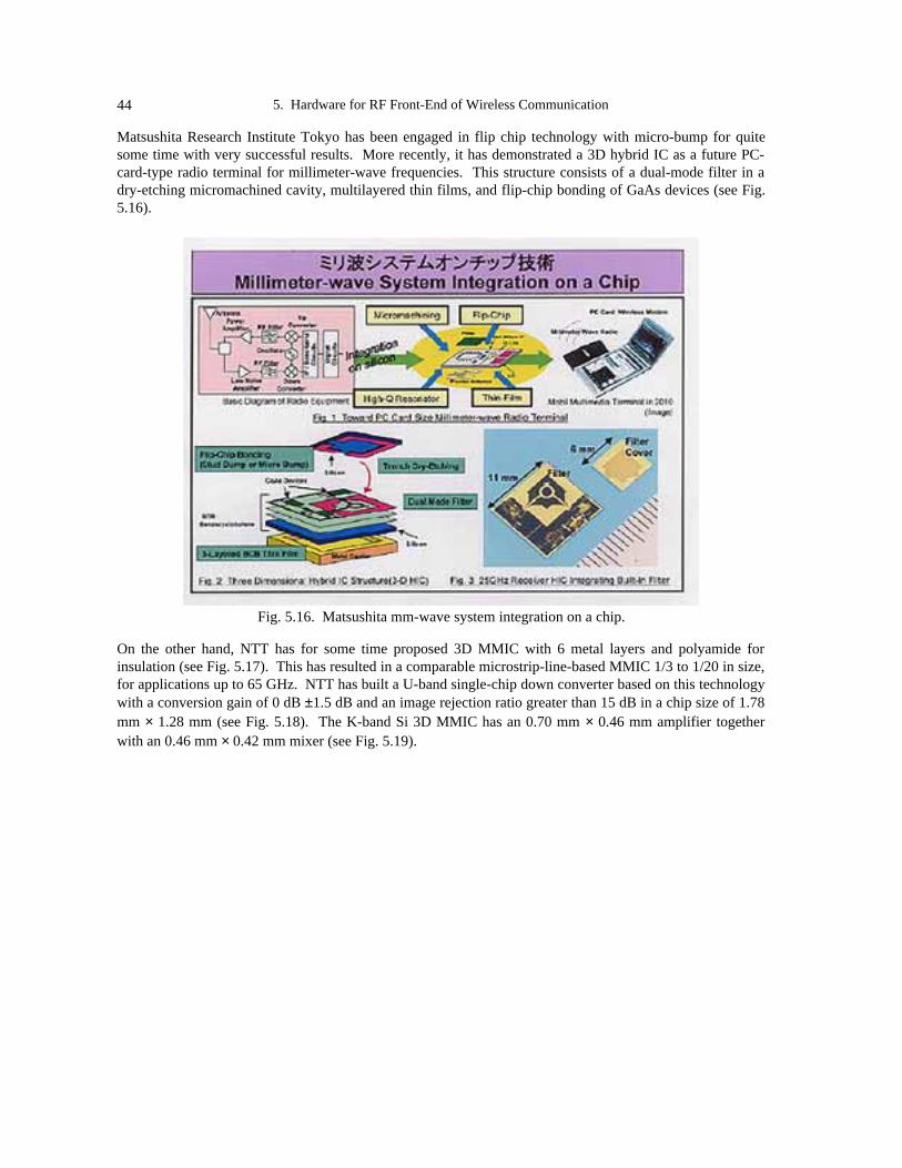
5. Hardware for RF Front-End of Wireless Communication44
Matsushita Research Institute Tokyo has been engaged in flip chip technology with micro-bump for quitesome time with very successful results. More recently, it has demonstrated a 3D hybrid IC as a future PC-card-type radio terminal for millimeter-wave frequencies. This structure consists of a dual-mode filter in adry-etching micromachined cavity, multilayered thin films, and flip-chip bonding of GaAs devices (see Fig.5.16).
Fig. 5.16. Matsushita mm-wave system integration on a chip.
On the other hand, NTT has for some time proposed 3D MMIC with 6 metal layers and polyamide forinsulation (see Fig. 5.17). This has resulted in a comparable microstrip-line-based MMIC 1/3 to 1/20 in size,for applications up to 65 GHz. NTT has built a U-band single-chip down converter based on this technologywith a conversion gain of 0 dB ±1.5 dB and an image rejection ratio greater than 15 dB in a chip size of 1.78mm × 1.28 mm (see Fig. 5.18). The K-band Si 3D MMIC has an 0.70 mm × 0.46 mm amplifier togetherwith an 0.46 mm × 0.42 mm mixer (see Fig. 5.19).

Tatsuo Itoh, Linda Katehi 45
Fig. 5.17. NTT’s concept on 3D MMIC.
Fig. 5.18. NTT U-band single-chip down converter.

5. Hardware for RF Front-End of Wireless Communication46
Fig. 5.19. NTT K-band Si 3D MMIC examples.
The millimeter wave band is expected to be a frequency resource for the next generation’s mobilecommunication system and is aimed at achieving a high-frequency PC-card-type radio terminal. To realizeall the wireless functions including the antenna and the filter on a chip, a 3D hybrid IC structure is one of themost effective solutions. Matsushita has recently developed a 3D millimeter-wave IC that uses siliconmicromachining. For the development of this IC, several technologies were used, including a dual moderesonant filter, multi-layer thin-films on silicon, and flip-chip bonding for the GaAs devices. This circuit hasbeen utilized in a 25 GHz receiver down-converter and has an area of 11 mm2 including the built-inmicromachined filter.
With the progress of technology and the invention of the transistor, it became apparent that very smalltransmission lines compatible with the planar technology of the newly discovered two- and three-terminaldevices are needed to effectively couple the power of microscopic devices and macroscopic systems. Circuitminiaturization can be achieved by use of 3D integration where circuits are laid in all dimensions of thespace. This approach has been effectively used in designing microprocessors and has resulted in a dramaticreduction of size and an unbelievable increase of speed. The next leap beyond the current state of the artmultichip modules (MCMs) is the development of a technology that can integrate high-frequency Si-basedactive circuits, advanced micro-electromechanical (MEMS) devices, and micromachined components (e.g.,filter/multiplexers) into one wafer. By employing 3D integration, significant reduction in mass (by a factorof 10) in physical volume and in cost can be achieved easily.
New concepts in integrated conformal packaging have been introduced, leading the way for micromachiningto impact planar microwave circuits beyond the component level and into the system integration area.Micromachining has the potential to revolutionize microwave devices by offering new techniques that can beused to integrate entire systems onto a single IC. One scenario for total system integration calls for the useof multiple layers to accomplish various system functions such as amplification, signal reception, downconversion, and filtering. Micromachining offers the possibility of connecting these multiple layers togethervertically to achieve new levels of high density integration. This concept has already been applied to the
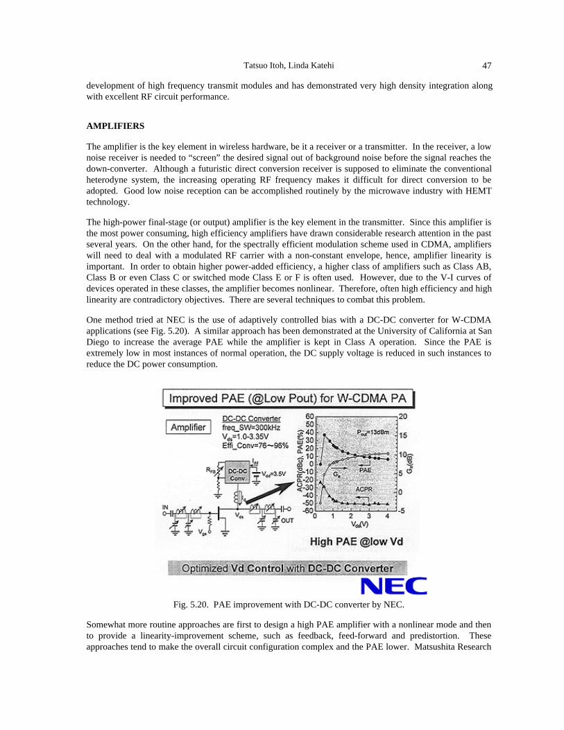
Tatsuo Itoh, Linda Katehi 47
development of high frequency transmit modules and has demonstrated very high density integration alongwith excellent RF circuit performance.
AMPLIFIERS
The amplifier is the key element in wireless hardware, be it a receiver or a transmitter. In the receiver, a lownoise receiver is needed to “screen” the desired signal out of background noise before the signal reaches thedown-converter. Although a futuristic direct conversion receiver is supposed to eliminate the conventionalheterodyne system, the increasing operating RF frequency makes it difficult for direct conversion to beadopted. Good low noise reception can be accomplished routinely by the microwave industry with HEMTtechnology.
The high-power final-stage (or output) amplifier is the key element in the transmitter. Since this amplifier isthe most power consuming, high efficiency amplifiers have drawn considerable research attention in the pastseveral years. On the other hand, for the spectrally efficient modulation scheme used in CDMA, amplifierswill need to deal with a modulated RF carrier with a non-constant envelope, hence, amplifier linearity isimportant. In order to obtain higher power-added efficiency, a higher class of amplifiers such as Class AB,Class B or even Class C or switched mode Class E or F is often used. However, due to the V-I curves ofdevices operated in these classes, the amplifier becomes nonlinear. Therefore, often high efficiency and highlinearity are contradictory objectives. There are several techniques to combat this problem.
One method tried at NEC is the use of adaptively controlled bias with a DC-DC converter for W-CDMAapplications (see Fig. 5.20). A similar approach has been demonstrated at the University of California at SanDiego to increase the average PAE while the amplifier is kept in Class A operation. Since the PAE isextremely low in most instances of normal operation, the DC supply voltage is reduced in such instances toreduce the DC power consumption.
Fig. 5.20. PAE improvement with DC-DC converter by NEC.
Somewhat more routine approaches are first to design a high PAE amplifier with a nonlinear mode and thento provide a linearity-improvement scheme, such as feedback, feed-forward and predistortion. Theseapproaches tend to make the overall circuit configuration complex and the PAE lower. Matsushita Research

5. Hardware for RF Front-End of Wireless Communication48
Institute Tokyo reported a new approach called the Hybrid Adaptive Predistortion method shown in Fig.5.21.
Fig. 5.21. Hybrid adaptive predistortion method by Matsushita.
A recent trend is to cope with the linearity-PAE issue from the point of “transmitter unit” rather than a singleamplifier. The above examples include a control or signal processing circuit in the configuration.
ANTENNAS
The antenna is a constant subject of discussion, but as yet no perfect solution has been found for wirelessapplications. There are many varied antennas from one-dimensional (dipole or monopole), two-dimensional(inverted F and microstrip patches), and 3D (dielectric antennas). In addition, dishes and phased arrays areused for base stations and satellite based communication. In this section, only the hardware aspect will bereported while the software aspects, such as the smart antenna or software antenna, will be discussed inChapter 6 of this report. Also, as many efforts on the antennas are quite similar, the reports are intended toprovide the descriptions below only as typical examples.
NTT’s multisector monopole Yagi-Uda (MS-MPYA) consists of two very low profile 12- and 6-sector unitsfor operation at 19 GHz. The 12-sector unit has a gain of 14 dB, and the 6-sector unit has a 10 dB gain.These units are used for beam forming, as Fig. 5.22 shows.

Tatsuo Itoh, Linda Katehi 49
Fig. 5.22. NTT’s multi sector monopole Yagi-Uda.
NTT has developed rod-type small-sized antennas for 25 GHz applications. Microstrip antennas are printedon panels within the rod, the beam radiating out from a cylindrical disk-like radome on top of it (Fig. 5.23).
Fig. 5.23. NTT’s rod type printed antenna.
At IMST, the effect of the human head on the antennas has been investigated extensively. It was found that8 ~ 10 dB loss is caused by the human head in an experiment at 450 MHz. IMST tested the efficiency ofseveral antennas. IMST’s helix antenna has 38% efficiency while its end-inductance antenna provided 84%.A ¼ wavelength patch has proven to be twice as efficient as the helix structure. IMST has also tried aceramic antenna for 0.9 and 1.9 GHz and have found that the bandwidth is too narrow.
Parabolic dishes still play an important role for wireless communication, especially for satellite-basedcommunication. NTT has developed several deployable on-board antennas (constructed of solid, wire-mesh)that are inflatable. NTT’s current non-inflatable mesh model consists of 7 modules, 10 meters in diameter,and weighing about 80 kg. The target is 14-modules 14 to 15 meters in diameter and 120 kg in weight. Thistechnology was successfully transferred to NASDA (Japanese counterpart of NASA).
CONCLUDING REMARKS
Throughout this study and visits to selected sites in Europe and Japan and interactions with selected U.S.industries, the WTEC panel recognized that hardware technologies for future wireless applications providesubstantial research opportunities on a worldwide scale. The following technological areas are eitheremerging or evolving and are considered important for the future health of wireless technologies:
• devices and materials
− new materials and components (GaN, SiGe, MEMS, substrate materials, etc.)

5. Hardware for RF Front-End of Wireless Communication50
− higher ft and fmax as well as higher linearity for active devices
− new 3D oriented process technologies
− higher performance passive components
− broadband antennas, higher gain antennas, low cost phased arrays
• front-end architecture
− amplifier linearization and efficiency
− interconnects and packaging
− mixed signal IC (baseband/RF)
− front-end architecture for software oriented radio
− RF aspects of smart antennas
− multifunction/reconfigurable devices/circuits/antennas
− MEMS RF components
• frequency of operation
− 10, 35, 60, 77, and 95 GHz
• CAD
− global CAD (circuits, electromagnetics, devices, antennas, thermal, mechanical, packaging allinclusive and interactive)
Some specific additional features are as follows:
Amplifier efficiency and linearity are contradictory requirements. The typical approach is to design anamplifier operated in a nonlinear mode and then provide schemes to improve linearity. The latter can be asimple output power back-off or a more sophisticated feed-forward or predistortion technique. In any case,not only good devices but also synergistic approaches are essential. It is important to optimize the amplifierblock or transmitter containing an amplifier and output circuits including antenna, or to make use of digitaltechnology for “signal processing” for the amplifier. Modulation format often dictates the choice of control.For instance, a spectrally inefficient constant-envelope modulation is very resistive to nonlinear effects.Combining digital techniques with an amplifier may lead to a form of “software” oriented radio.
A mixed signal IC may be a good ingredient for a futuristic one-chip radio or system-on-a-chip. But bothgood devices and also low loss and high isolation interconnects are needed.
Software oriented radio has drawn much attention. However, often software issues and digital circuits issuesare emphasized while the RF front end is sometimes neglected. Therefore, front-end architecture should beincluded in the studies for software radio.
Smart antennas are another example where the software and hardware collaborate well. Integrated antennasalleviate some of the hardware difficulties associated with smart antennas. Also, reconfigurable circuits andantennas should play important roles in developing the smart antenna.
Three-dimensional integration schemes are required to provide communication systems that are very small,very low in weight and very low in cost without compromising performance. The use of heterogeneousmaterials for the circuits and devices incorporated in the system may lead to unique solutions in integrationand packaging.
High-Q, low-loss passive devices are also needed for high performance. The development of RF MEMSalso provides new directions with the possibility of new functions and system architectures.

Tatsuo Itoh, Linda Katehi 51
The above are some of the possible future directions of research. What should be emphasized is that futureresearch must require interdisciplinary approaches not only in terms of different hardware components butalso hardware and software.
TECHNOLOGY ASSESSMENT
It is always difficult to make a comparable assessment of the technical advances of several countries andregions. The hardware technologies for wireless communication are no exception. In fact, due to the verybroad technical topics involved in this chapter, the challenge is even greater. Therefore, Table 5.1 providedbelow is based on the quite subjective judgment of the authors of this chapter. The WTEC panel as a wholedoes not disagree with this table.
Table 5.1Wireless Technology Assessment for Hardware
U.S. Japan Europe
Millimeter Wave Circuits and Systems ** ***** *****
Packaging/Interconnect ***** **** ***
CAD ***** ** ***
SiGe/Si **** *** *****1
III-V ***** ***** ****
GaN **** **** ***
Antennas *** **** ***
Passive Components **** ***** ****
Amplifier Technique ***** **** ****2
MEMS/Micromachining **** *** **
1 Germany only; 2 UK activities
The following six points pertain to the entries in Table 5.1:
1. Millimeter Waves. Here, it is very clear that in terms of devices and MMICs, the United States is aheadof others, largely because of DARPA’s successful MIMIC and MAFET projects. However, the U.S.entry here reflects expertise in millimeter wave circuits for non-military wireless applications. In Japan,government-led programs on 60 GHz wireless technology have been implemented, while in Europe asubstantial effort has been expended mainly for automotive applications centered around 77 GHz.
2. The United States has dominated CAD development and commercialization and it maintains anunchallenged position.
3. In the area of SiGe, IBM is the leader. However, its circuit applications have lagged behind Daimler’seffort, particularly in millimeter wave areas. In an effort to make the process technology available toothers, IBM and Daimler process technologies are expected to benefit circuit design efforts funded byother organizations.
4. GaN is still in its infancy in industrial applications. Most high performance devices devices are still atthe research stage. It is interesting to note that the United States is leading in the RF (microwave) area,i.e., transistor development, while Japan’s effort has mainly been in the area of optical devices. Cree inthe United States and Nichiya in Japan have made excellent materials available.
5. Antenna research has left much to be desired. In wireless communications, antenna research is meant tobe different from the traditional in terms of the analysis, design, and characterization of antenna

5. Hardware for RF Front-End of Wireless Communication52
elements and/or phased arrays, from an electromagnetic point of view. What is needed is thedevelopment of an interdisciplinary research field useful for future wireless technologies. Examples arethe integration of antennas with the RF front end, such as passive filters, MEMS devices, amplifiers, andeven DSPs.
6. In the area of passive components, the Japanese are slightly ahead due to their effort in high Qcomponents led by Murata.
In closing, it should be emphasized that future research on wireless oriented hardware requiresinterdisciplinary approaches not only between hardware and hardware but also between hardware andsoftware.

53
CHAPTER 6
SMART ANTENNAS
Jack H. Winters
INTRODUCTION
Throughout the world, including the United States, there is significant research and development on smartantennas for wireless systems. This is because smart antennas have tremendous potential to enhance theperformance of future generation wireless systems as evidenced by the antennas’ recent deployment in manysystems.
This chapter covers smart antenna technology, including software and system aspects. First the two basictypes of smart antennas, adaptive and phased arrays, are described and then their current use and proposeduse in future wireless systems is discussed. Then the key research issues that came up at the U.S. workshopand at the various sites the WTEC panel visited are presented. Finally, conclusions are presented along withthe technology assessment of the U.S., European, and Japanese companies.
SMART ANTENNA DESCRIPTION
There are two basic types of smart antennas. As shown in Fig. 6.1, the first type is the phased array ormultibeam antenna, which consists of either a number of fixed beams with one beam turned on towards thedesired signal or a single beam (formed by phase adjustment only) that is steered toward the desired signal.The other type is the adaptive antenna array as shown in Fig. 6.2, which is an array of multiple antennaelements, with the received signals weighted and combined to maximize the desired signal to interferenceplus noise power ratio. This essentially puts a main beam in the direction of the desired signal and nulls inthe direction of the interference.
A smart antenna is therefore a phased or adaptive array that adjusts to the environment. That is, for theadaptive array, the beam pattern changes as the desired user and the interference move; and for the phasedarray the beam is steered or different beams are selected as the desired user moves.
Nearly every company the WTEC panel visited is doing significant work in smart antennas. Indeed, somecompanies placed strong emphasis on this research. In particular, researchers at NEC and NTT stated thatthey felt that smart antenna technology was the most important technology for fourth generation cellularsystems. Researchers at Filtronics and other companies agreed that smart antenna technology was one of thekey technologies for fourth generation systems. The reasons appear below.

6. Smart Antennas54
DESIRED SIGNAL
SIGNAL OUTPUT
Fig. 6.1. Phased array.
DESIRED SIGNAL
SIGNAL OUTPUT
BEAMFORMER WEIGHTS
INTERFERENCE
Fig. 6.2. Adaptive array.
FUTURE WIRELESS SYSTEM REQUIREMENTS
Future wireless systems generally may require higher data rates with better coverage for a wide variety ofusers operating with a large variety of different systems. To achieve these goals, greater power, interferencesuppression, and multipath mitigation are needed. As users operate at higher data rates, they need higherpower for adequate reliability. For higher bandwidths, higher carrier frequencies that have higherpropagation and circuit losses are needed. So some way to recover this power must be developed. Inaddition, interference suppression is needed for higher capacities. Particularly as higher frequency reuse isused to increase capacity, there will be more cochannel interference, which requires greater interferencesuppression. Finally, multipath mitigation to have more reliable and robust communications is necessary.

Jack H. Winters 55
SMART ANTENNA ADVANTAGES
Smart antennas can help systems meet these requirements in the following manner: First, both phased andadaptive arrays provide increased power by providing higher gain for the desired signal. Phased arrays usenarrow pencil beams, particularly with a large number of antenna elements at higher frequencies, to providehigher gain (power) in the direction of the desired signal. Adaptive arrays place a main beam in the directionof the desired signal for an M-fold power gain with M antenna elements.
In terms of interference suppression, phased arrays reduce the probability of interference with the narrowerbeam, and adaptive arrays adjust the beam pattern to suppress interference. For multipath mitigation, smartantennas can provide diversity, of which there are three basic types: spatial, polarization, and angle (orpattern) diversity. These appear in more detail below.
USE OF SMART ANTENNAS
From the site visits and U.S. company workshop, it appears that phased arrays and adaptive arrays areconsidered and researched about equally. Although some companies studied only one type exclusively,others work both on phased and adaptive arrays.
Phased arrays are mainly being studied for point-to-point wireless systems, e.g., for wireless local loops.They are also being considered for macrocellular base stations. For example, in Europe there is work onusing 8-element phased arrays on GSM base stations. In Japan, there is work on using very large phasedarrays on satellites, as well as on satellite terminals such as on car tops.
Adaptive arrays are being studied for indoor systems, i.e., systems with wide angular spread where thereceived signals arrive via widely separated paths where a phased array may not be useful in achieving gain.Also they are being studied in microcells and in some cellular base stations. For example, currently in theTDMA system ANSI-136 adaptive antenna algorithms have been widely deployed commercially in theUnited States. Also adaptive arrays are being considered on cellular terminals where local scattering causeswide angular spread.
KEY RESEARCH ISSUES
The site visits and the U.S. workshop raised several key research issues.
The first research issue is cost, including the cost of power. For example, at Philips, researchers noted that50% of the power in the handset is in the RF electronics. Therefore, multiple antennas in the handset notonly increase the dollar cost of the handset, but also increase the power and thus decrease battery life.Research to reduce the power that each of these antennas requires needs to be undertaken. Similarly, thenumber of required receiver chains must be reduced because the RF electronics and the A/D converterrequired with each antenna are expensive. One method being considered is a low-cost phased array. Athigher frequencies, some companies are considering using large phased arrays to create very narrow beamsto provide higher gain. But the issue is how to have, for example, hundreds of antenna elements and massproduce them at a reasonable cost. Thus, cost is limiting the number of antenna elements that can be used.Various solutions are being considered. For example, ATR is considering using optical beamforming forlarge phased arrays. Another solution being considered is integrating the antennas onto the RF electronicsIC itself. Also, researchers at Ericsson are considering a limited introduction of smart antennas, becausetheir research has shown that using smart antennas at just a small portion of the base stations, e.g., thosehaving capacity problems or creating the most interference, can achieve most of the gain of completedeployment. In particular, Ericcson’s results show that deploying smart antennas at only 10% of the basestations resulted in a 40% increase in capacity.

6. Smart Antennas56
The second key research issue is size. Large base station arrays are difficult to deploy for aesthetic reasons,and multiple external antennas on terminals are generally not practical. For base stations, companies areusing dual polarization, but at the terminal some companies are researching putting antennas on the RFelectronics IC in an “antenna-less” terminal (since an external antenna is not present). However, issues ofgain and efficiency and the effect of hand placement on the terminal need further research.
The third issue is diversity, which, as discussed above, is needed for multipath mitigation. For diversity,multiple antennas are needed on the base stations and/or terminals. As mentioned above there are three typesof diversity: spatial, polarization, and angle (pattern) diversity. Spatial diversityspatial separation of theantennasis difficult on a small handset. Even though only a quarter wavelength separation is required forlow correlation of the multipath fading between antennas on a handset, it also is difficult for base stationswhere the angular spread is small and large separation is required for low correlation. Spatial diversity iseven more difficult to achieve in point-to-point systems where a near line-of-sight exists between thetransmitter and receiver, and, further, at higher frequencies, sufficient spatial separation does not appearfeasible. This problem can be partially avoided by the use of polarization diversity, where both vertical andhorizontal polarizations are used to obtain dual diversity without spatial separation. For example, at Philipsand other companies, researchers are using dual polarization diversity on handsets. Others are studying andimplementing dual polarization on base station antennas. Polarization diversity provides only dual diversity,though polarization diversity can be used in combination with other forms of diversity to obtain higherorders of diversity.
Finally, companies are using angle diversity. That is, the signals from two or more beams (generally thebeams with the highest signal powers) are used to obtain diversity. But performance depends on the angularspread. If the angular spread is small, then the received signal is mainly arriving on one beam and anglediversity will not provide a significant diversity gain. Also, some companies are studying pattern diversity,where antennas have different antenna patterns. In particular, researchers at Nokia are studying the use ofmultiple antennas in the handset, where some of the antennas may be covered by the hand, and moving thehand around changes the antenna pattern. These researchers believe that by adaptively combining thesignals from such antennas, perhaps only using those antennas not blocked by the hand or adjusting theantenna impedance to compensate for hand placement, it may be possible to obtain much better performance(including diversity) with multiple internal antennas as compared to an external antenna.
A fourth issue is signal tracking, i.e., determining the angle-of-arrival of the desired signal with phasedarrays to determine which beam to use and adjusting the weights with adaptive arrays to maximize thedesired signal-to-noise-plus-interference ratio in the output signal. At none of the sites the panel visited didthe researchers feel that signal processing power was a significant issue for tracking in future systems.Instead, they felt that increases in signal processing power would permit new tracking algorithms to beimplemented without substantial consideration of the processing requirements. Researchers at Ericsson, forexample, noted that, although angle-of-arrival techniques for phased arrays use MUSIC or ESPRITalgorithms in 2000, improvements are needed to make these algorithms more robust with angular spread andto obtain higher resolution. For adaptive arrays, better subspace tracking methods are needed since higherdata rates will require longer temporal equalizers, which require longer training sequences and greateroverhead.
A fifth issue is spatial-temporal processing, i.e., equalization of intersymbol interference due to delay spreadat high data rates, with cochannel interference suppression. During the WTEC panel’s European site visits itwas noted that better architectures are needed for spatial-temporal processing, as current architectures haveroom for significant improvement. However, the use of OFDM is being considered for fourth generationsystems (as brought up during Japanese site visits), which may simplify spatial-temporal processing at highdata rates, but further research is needed. Also, space-time coding is an area of significant research,primarily in the United States, but research on improved interference suppression and tracking with thesecodes is needed. Finally, multiple transmit/receive antenna systems (referred to as multiple input multipleoutput (MIMO) or BLAST for the Lucent Bell Labs version) are being touted mainly in the United States as

Jack H. Winters 57
a means for achieving very high capacities in wireless systems. With MIMO, different signals aretransmitted from each antenna simultaneously in the same bandwidth and then are separated at the receiver,thus increasing the potential to provide an M-fold increase in capacity without an increase in transmit poweror bandwidth. For example, Lucent has demonstrated 1.2 Mbps in a 30 kHz channel in an indoorenvironment using 8 transmit and 12 receive antennas. To be useful in a wider variety of wireless systems,however, research is needed to extend the technique to the outdoor environment, including determining themultipath richness of this environment, which is required for the technique to work properly, and to thecochannel interference environment of cellular systems.
A sixth issue involves putting the necessary hooks in the standards such that smart antenna technology canbe used effectively. In second generation cellular systems, ANSI-136 and IS-95, implementing smartantennas had problems because the standards did not consider their use. In particular, ANSI-136 required acontinuous downlink signal to all three users in a frequency channel, which precludes the use of differentbeams for each of these three users. In IS-95, there is a common downlink pilot, which also precludes theuse of different beams for each user, as all users need to see the pilot. For third generation systems, smartantennas were taken into account in WCDMA, where downlink pilots are dedicated to each user, andtherefore smart antennas can be effectively used on the downlink. In the EDGE system, the continuousdownlink requirement is no longer present, but some signals from the base station still need to be broadcastto all users. Thus, further research is needed to ensure that smart antennas can be effectively used in thissystem. For fourth generation systems, therefore, smart antennas must be taken into account in standarddevelopment. Specifically, any packet or multimedia access to all users, as well as pilots, must betransmitted or done in such a way as to not preclude the use of smart antennas, if this technology is to beused to its full benefit. Since these standards are international, research in this area needs to be doneglobally.
The previous issue leads to the seventh and final issue: vertical integration or an interdisciplinary approach.Research on smart antennas will require multiple factors/expertise to be considered—smart antennas cannotbe studied in isolation. This issue was brought up repeatedly during the WTEC site visits. As discussedabove, smart antennas must be considered in protocol development, i.e., expertise in both physical and mediaaccess layers is required. Also, smart antennas need to be considered in combination with other techniques,such as frequency hopping, power control, and adaptive channel assignment. Researchers at Nokia andPhilips noted that smart antennas need to be considered in combination with RF matching, particularly withmultiband antennas. At Nokia, the issue of adapting the antennas to hand position was noted. Ericsson hasstudied the limited introduction of smart antennas with nonuniform traffic. Another issue was the interactionwhen ad hoc networks are used. Furthermore, propagation measurements and channel modeling are neededto determine the performance of smart antennas in specific environments. Issues of base station versusterminal antenna (complexity) tradeoffs were also noted, as well as transmit diversity with space-timecoding. From the above issues, it seems important that smart antenna research be multidisciplinary.However, few people have such a wide range of expertise, and it is often difficult for researchers with suchdifferent expertise to work together effectively. Thus, even though the critical need for such research wasnoted over and over again worldwide, there were few instances in any region where this was being done, oreven planned in the future, as this type of research is different from the general method used in the past.Thus, this type of research appears to require a change of approach, but there was general agreement that thecompanies that can do this will make the greatest progress in smart antennas.
CONCLUDING REMARKS
From the site visits in Europe and Japan and interactions with U.S. companies, it appears that the majorrequirements for future wireless systems are higher data rates with better coverage to a large number of usersat a reasonable cost. To obtain these goals, higher signal-to-noise ratios (more power), interferencesuppression, and multipath mitigation is needed. The smart antenna was universally recognized as a criticalcomponent in meeting these requirements, but much research still needs to be done, as evidenced by the factthat nearly all sites visited have a significant research effort in smart antennas. Research efforts are about

6. Smart Antennas58
equally divided between the two types of smart antennas (phased arrays and adaptive arrays), although theemphasis varies among companies.
The WTEC study concludes that the major research issues for smart antennas are the following:
• cost (including power and electronics)
• size
• diversity
• tracking
• spatial-temporal processing
• hooks in international standards to include provisions for smart antennas
• vertical integration/interdisciplinary research
Of these, interdisciplinary research incorporating smart antennas was considered to be the key to the greatestgains, but very little of this type of research is currently being conducted because of the difficulty of therequired interactions.
For future wireless systems to be viable, substantial research on smart antennas in the above areas will berequired, with emphasis on interdisciplinary approaches.
TECHNOLOGY ASSESSMENT
Smart antenna technology varies substantially among companies, and since many of these companies aremultinational, it is difficult to make a comparative assessment of the technology among regions. Nearly allwireless companies visited, and therefore regions, have significant research in smart antennas, and thusoverall the current status of the regions in smart antennas appears to be about equal. However, the emphasisof the research on phased or adaptive arrays varies by application. Specifically, Japanese companiesemphasize WCDMA and higher frequencies, and thus the major focus of their work is on phased arrays. Onthe other hand, U.S. and European companies tend to emphasize lower frequencies (850 and 1900 MHz),and TDMA systems (GSM, EDGE, ANSI-136) as well as WCDMA, and therefore focus on adaptive arraysin addition to phased arrays. Thus, Japan leads in smart antenna research and technology for phased arrays,particularly at higher frequencies (5 GHz and above), whereas the United States and Europe lead in adaptivearray research and technology (see Table 6.1).
Table 6.1Technology Comparison
U.S. Japan Europe
Smart Antennas Overall ***** ***** *****
Phased Arrays *** ***** ***
Adaptive Arrays ***** *** *****
59
CHAPTER 7
HOLISTIC DESIGN OF WIRELESS SYSTEMS
Ramesh Rao
INTRODUCTION
The phenomenal growth in mobile wireless communications combined with the equally impressive globalgrowth in Internet-related services and applications is poised to effect fundamental changes in all walks oflife. With this newfound success comes the need to cope with the demand for services that far exceeds earlyprojections. Much of this growth was fueled by early research funded by federal agencies and privateindustry. Yet the need to reexamine and identify new areas will enable the next generation of innovations.This report covers three related developments, software radios, energy and power management techniques,and integrated approaches to system design.
SOFTWARE RADIOS
In contrast to conventional radios, software radios process signals mostly in the digital domain, making itpossible to put radio under software control. A number of companies in Japan and Europe described theirrationale for software radios and outlined areas of research that were viewed as critical for the developmentof software radios. Alcatel, NTT, Daimler-Chrysler, NEC, Toshiba, Matsushita, Philips, Nokia, IMST allreported ongoing research and development activities on software radios. U.S. companies that describedefforts in this regard included Hughes and Rockwell Collins. At the time of the WTEC study, mostcompanies viewed software radios as reconfigurable, multimodal, multichannel, or multiband devices. Thisview does not call for radios that dynamically alter error control algorithms or modulation formats as afunction of the channel and traffic characteristics.
The development of a reconfigurable, multimodal, multichannel or multiband radio depends critically onhigh resolution, high bandwidth, high dynamic range, A/D converters. Marcell Pelgrom at Philips hasforecast that the trend in higher resolution/bandwidth A/D converters will continue for another six to tenyears, with three orders of magnitude improvement still left. Besides A/D converters, Alcatel drew attentionto the need for frequency synthesizers and good integrable low noise amplifiers (LNAs) as additionalenablers for software radios.
Dr. Hori at NEC described an interesting application of the software radio concept by calling for studies ofsystems in which reconfigurable radios are deployed only at base stations and not in the handsets. Basestation radios would then be expected to recognize the handset type and adjust themselves to the protocoland system for which the terminal was designed. This would obviate the need for reconfigurable radios inhandsets and allow for smaller and cheaper handsets.
7. Holistic Design of Wireless Systems60
Bo Hedberg at Ericsson, speaking about the power efficiency of multicarrier power amplifiers, reinforcedDr. Hori’s view of the asymmetric deployment of software radios. Hedberg also concentrated on the basestation, because he thought that the software radio solution is very costly for terminals. The technologyneeds to mature before it can be used at the terminals. Hedberg pointed out that power efficiency isimportant, not just at the mobiles but also at base stations. Apparently, the air conditioning required to keepthe multi-carrier power amplifiers (MCPAs) cool at the base stations would increase the price significantly.Hedberg estimates that half the cost of future base stations will be in the MCPA. Hedberg concluded that alot of research will be needed during the next several years to improve the MCPAs.
Assessment
State of the art
At the time of the WTEC study, the companies visited viewed software radios as enabling the production ofmultimodal, multichannel or multiband terminals. The focus is on using a software reconfigurable terminalto harmonize dissimilar standards in one lightweight, low cost package that can be mass produced andreconfigured in software. The realization of this relatively modest objective requires additional progress on(1) high resolution, high bandwidth, high dynamic range A/D converters, (2) frequency synthesizers, and (3)better low noise amplifiers.
For a time, software radios are likely to be deployed only at base stations. In this scenario, the subscriberwould be shielded from the high cost, complexity, and power requirements of software radios. A primaryadvantage of such an asymmetric deployment is the ability to support older generation handsets even asservice providers roll out newer generation services.
The base station’s ability to sense and adjust to the terminal’s capabilities (protocol, frequency band etc.)could be used to create new competitive models for cellular services in which users, regardless of the type ofterminal they carry, can roam across competing systems. This would be in contrast to approaches in whichsubscribers have to make a hard decision between competing providers that use incompatible air interfacesand offer very good coverage limited to certain geographical regions. Such a model may help the cellularindustry as a whole to grow by offering more assured service to subscribers.
Once hardware requirements for the current generation of software radios have been met, the rationale forsoftware radios will evolve from lowering costs to enhancing performance at lower cost as the demand forservices starts to expand and saturates the available capacity. This objective will require more adaptivesoftware radios that will be capable of switching quite rapidly between modulation formats, error controlalgorithms and other such features as a function of the channel, traffic and possibly battery characteristics.The additional technical breakthroughs required will be in the area of software control of the underlyinghardware.
Deployment Trends
The task of assessing the relative status of U.S. companies in the global arena is fraught with limitations.The need to provide global communications services provides a strong incentive for telecommunicationscompanies to operate as global enterprises. Therefore at a certain level, the distinction between U.S.,European, and Japanese companies is quite artificial. Yet, in the context of communications, it is quiteinstructive to examine the relative impact of regulatory developments, which do differ from nation to nation,on technological needs.
In an article titled “ Software radio technology: a European perspective,” Tuttlebee (1999) argues that theneed for software radios is most acute in the United States where multiple second generation digital systemscompete in a market that has yet to be saturated. Such a market could be more efficiently served through theuse of software reconfigurable handsets. On the other hand, European standardization of GSM obviates theneed to develop software reconfigurable for multimodal, multi-standard handsets since the European

Ramesh Rao 61
multiband GSM allocations can be accommodated with modest enhancements at the RF end withoutincorporating the full range of reconfigurations that software radios may be called upon to effect in the U.S.market. Therefore, Tuttlebee claims that software radios are likely to emerge first in the United States andthen in Europe when there is a demand to support user roaming between GSM and third-generation UMTSsystems.
Publication Trends
To get a sense of the current state of the research activity, the WTEC panel analyzed publications onsoftware radios that have appeared in the recent literature, using the online INSPEC service, which tracks“articles in over 4000 scholarly, journals, conference proceedings, books, reports, and dissertations inphysics, electrical engineering and electronics, computers and control, and information technology.” Over1400 publications on “software radio” appeared during the period 1995 to 1999almost one newpublication per day.
Of these 1400 publications,
• 284 covered architecture
• 235 covered RF elements
• 178 covered protocols
• 146 covered DSP algorithms
• 127 covered antennas
• 75 covered base stations
• 20 covered batteries
• only 15 included any coverage of handsets.
With regard to author affiliations,
• about 40% listed U.S. institutions
• 35% listed institutions in Germany, the United Kingdom, Italy, France, Finland, Sweden or theNetherlands
• 5% listed Canadian institutions or others
• 5% listed Japanese institutions
All but 90 of the 1400 publications were in English. Of the 90 non-English publications, 27 were inJapanese.
These numbers suggest that current publications activity is largely in line with the software radio needscommunicated to the WTEC panelists: RF components, smart antennas, protocols, DSP algorithms and basestation deployment. U.S. leadership in the field appears to be consistent with Tuttlebee’s assessment of thecritical need for early deployment of software radios in the United States. The extensive Japanesedevelopment activities discovered by this panel during the site visits appear not to be reflected inpublications.
Summary Assessment
Factoring in all the information available at this time, the WTEC panel concluded that U.S., European, andJapanese companies were on par with regard to software radio technology.

7. Holistic Design of Wireless Systems62
POWER AND ENERGY MANAGEMENT
Power and energy management issues came up in a variety of contexts including software radios.
Addressing the issue of power management in a broader context, Marcel Pelgrom at Philips noted the trendtowards higher energy per weight and size through the evolution of batteries from NiCd to Lithium-ion toLithium-polymer and beyond. Hans Hofstraat, also at Philips, discussed polymer batteries, which in 5-10years could be widely deployed and reduce costs dramatically. However, Hofstraat, who passed around aworking polymer display driven by a polymer battery, believes that substantial research is still needed,particularly multidisciplinary research.
The success of untethered, mobile communications depends critically on portable energy sources that enjoy along life. Longer battery life can be effected directly through the development of higher capacity cells but,so far, advances in battery technology have failed to keep up with the rapid pace of developments in otheraspects of mobile communications. Thus, energy savings may more likely be found through more efficientmanagement of available battery energy.
Pelgrom claimed that the best research area for power management was better power management throughprotocols. Pelgrom also observed that RF power consumption often dominates software powerconsumption. He felt that long-term research should emphasize RF and packaging research and softwareimprovements that have a direct effect on RF power consumption. Nokia representatives pointed out that thedrivers of technologies in the future will be service and application protocols and not more capacity (as is thecurrent driver) and identified battery and energy management as one of the technologies needed to achievethese applications. Mitsubishi Electric Corporation’s overarching concern for reducing the size and weightof handsets induced them to explore battery technologies to extend life or reduce weight. U.S. companiesthat are interested in the topic include IBM, Hughes, Rockwell Collins, and Maxim.
Assessment
Development of higher capacity electrochemical cells has failed to keep pace with the demand. Therefore itis desirable to develop energy efficient architectures, systems, protocols, algorithms, and circuits for theefficient management of available battery energy.
Currently, the energy consumed in RF processing dominates digital processing. Technology areas in thecritical path include (1) RF and packaging advances, (2) software that reduces RF power consumption, (3)energy efficient modulation formats and protocols, and (4) power efficient hardware-software co-design.Low cost polymer batteries appear to be an innovative development on the battery technology side, but theneed for more extensive multidisciplinary research on the topic persists.
As networks reach deeper, penetrating home and commercial control applications, many simple non-computing nodes will need to be networked. Such an approach is expected to result in new services andapplications. Current initiatives, such as Bluetooth, HomeRF, and sensor networks, are early precursors ofthis trend. In sensor networks or any largely dormant segment of a network, battery powered nodes will bemostly asleep and consequently consume most of their energy while asleep. Therefore research on ways toreduce energy consumption in sleep modes is critical. This means that RF energy consumption is not theonly limiting factor.
The panel agreed that United States and European companies were on par with regard to their interest inenergy efficient system designs. The Japanese companies that the panel visited did not articulate any specialconcern in this regard. Many of the leading suppliers of batteries for portable devices are currently Japanese.
Ramesh Rao 63
INTEGRATED APPROACHES TO WIRELESS SYSTEM DESIGN
Over the years, the layering principle, which segments network functions and specifies standard interfacesbetween layers, has served the networking community quite well. The standardization of functionalinteractions between the layers has, to some extent, allowed developers to work independently of each other.This has led to the development of multiple sources for protocols and new market-driven approaches to theiruse and integration.
Three relatively recent phenomena have affected the way protocol stacks will have to be designed. First,protocol stacks are being used in new ways. Two examples are “best effort” IP over ATM stacks that canguarantee service quality and voice, which demands some quality guarantees, over best effort IP. Second,concepts such as quality of service guarantees and energy conservation, which can be engineered in multipleways at various layers, are emerging. Finally, concepts like software controlled radios and active networksthat can be used to redefine networking functions on the fly are being developed. These three sets ofdevelopments taken together stimulate the need for better understanding of the interaction between thelayers. IPSI, ATR, Mitsubishi, and NEC are working on these developments. Representatives of Hughes, aU.S. company, described its interests in this topic as well.
Mitsubishi researchers reported that their concern for reducing the size and weight of hand sets compels theexploration of cross layer opportunities for effecting efficient communications. At NEC, interest inprovisioning QoS, has led to a call for “definitions that work” and enhanced understanding of the functionalrelationships between levels in order to effect system optimization. At NEC, Dr. Hori articulated the need“to mix the software/system issues with hardware.” For instance, NEC has an interest in a system on a chipwith integrated antennas.
The objectives of ATR’s Adaptive QoS Management project are to develop adaptive ways in which networkparameters and resources are controlled in response to changing QoS demands in multimedia applications.The focus at ATR was on controlling the compression and transmission parameters of video streams (bit-rate, frame-rate, etc.) through negotiation among network agents that correspond to different user streams.Eventually these negotiations will include allocation of additional network resources (such as buffermemory, bandwidth, etc.). The investigators do realize that end-to-end QoS performance depends on thelower-layer (link) QoS parameters and intend to include this coupling in their methods.
The visit at IPSI highlighted the issues in wireless networking that are often ignored by the wirelesscommunity, namely the need to address the design of upper-layer protocols and their effects on linkoperation. However, the visit verified that an integrated approach to networking that bridges the gaps amonglayers is still needed, but not yet in place.
Assessment
A number of companies, especially those that were building prototypes, were keenly aware of the need todevelop a comprehensive understanding of design options regardless of the layer (of the system protocolstack) that the function traditionally resides in. The most pressing problems identified included (1) “QoSdefinitions that work,” (2) better understanding of the functional relationships between levels, (3) interlayerinteractions, and (4) ways to mix software, systems, and hardware issues. More focused research is requiredin order to understand the (1) effect of lower-layer (link) QoS characteristics on end-to-end QoSperformance and (2) the effect of upper-layer protocols on link operation. This research is necessary in orderto support more sophisticated negotiation between applications and networks.
From a larger perspective, the payoff from adopting integrated approaches may not be worth the cost ofdeconstructing the layered approach to protocol design. Indeed, layering protocol stacks has served well inthe past. Yet, developments that motivate new research include the following: (1) the notion of a link layeris much softer in the wireless environment than in a wire-line environment, (2) issues such as quality ofservice guarantees and energy conservation can be engineered in multiple ways at various layers and, finally,
7. Holistic Design of Wireless Systems64
(3) new uses for protocol stacks. These developments require better understood interactions between thelayers of a protocol stack as well as between different protocol stacks. Research on this topic is likely tofurther benefit from the availability of software controlled radios and the deployment of active networks thatcan be used to redefine networking functions on the fly.
Japanese companies seemed to display the highest sensitivity to this issue. Perhaps this is consistent withtheir early prototyping efforts. U.S. and European companies were on par with each other, but did not seemas advanced as the Japanese.
SUMMARY
ATR, Alcatel, Daimler-Chrysler, Ericsson, IPSI, IMST, Matsushita, Mitsubishi, NEC, Nokia, NTT, Philips.and Toshiba all reported activities in the areas of software radios, energy or power management, andintegrated approaches to wireless system design. The initial objectives described were technologically quitechallenging and were estimated to take at least five to 10 years to reach maturity and deserved to be nurturedin the research community.
These objectives included development of (1) high performance A/D converters, (2) frequency synthesizers,(3) low noise amplifiers, (4) low cost, long life batteries, (5) protocols that effect RF power economies, and(6) techniques to support differentiated service qualities in a wireless environment. Scenarios for thedeployment of a new generation of systems based on these initial initiatives are already under careful study.
Many activities in wireless system design will benefit from substantial research and development in the areaof integrated approaches to wireless systems. Finally, these initial initiatives, which tend to have a hardwarefocus, should lead to a second generation of integrated systems that will be driven by sophisticated protocols,algorithms, and other software techniques that will harness the full power of the adaptive hardware toproduce new services and applications. Some thought should be given to exploring these possibilities.
REFERENCE
Tuttlebee, W.H.W. 1999. “Software radio technology: a European perspective.” IEEE Communications 37 (2):118-123.

65
APPENDICES
APPENDIX A. PROFESSIONAL EXPERIENCE OF PANELISTS
Name: Anthony Ephremides (Panel Chair)
Address: Professor of Electrical Engineering & Institute for Systems ResearchDepartment of Electrical EngineeringUniversity of MarylandCollege Park, MD 20742-3285
Anthony Ephremides received his B.S. degree from the National Technical University of Athens (1967) andM.S. (1969) and Ph.D. (1971) degrees from Princeton University, all in electrical engineering. He has beenat the University of Maryland since 1971, and currently holds a joint appointment as Professor in theElectrical Engineering Department and in the Institute of Systems Research (ISR). He is co-founder of theNASA Center for Commercial Development of Space on Hybrid and Satellite Communications Networksestablished in 1991 at Maryland as an offshoot of the ISR.
He was a Visiting Professor in 1978 at the National Technical University in Athens, Greece, and in 1979 atthe EECS Department of the University of California, Berkeley, and at INRIA, France. During 1985-1986he was on leave at MIT and ETH in Zurich, Switzerland. He was the General Chairman of the 1986 IEEEConference on Decision and Control in Athens, Greece. He has also been the Director of the FairchildScholars and Doctoral Fellows Program, an academic and research partnership program in SatelliteCommunications between Fairchild Industries and the University of Maryland. He won the IEEE Donald E.Fink Prize Paper Award (1992). He has been President of the Information Theory Society of the IEEE(1987) and served on the Board of the IEEE (1989 and 1990).
Dr. Ephremides’ interests are in the areas of communication theory, communication systems and networks,queueing systems, signal processing, and satellite communications.
Name: Tatsuo Itoh (Panel Vice-Chair)
Address: Professor of Electrical EngineeringDepartment of Electrical EngineeringUniversity of California, Los Angeles405 Hilgard AvenueLos Angeles, CA 90095-1594
Tatsuo Itoh received the Ph.D. degree in Electrical Engineering from the University of Illinois, Urbana, in1969. He worked at the University of Illinois, Stanford Research Institute, University of Kentucky, AEGTelefunken in Germany, and the University of Texas at Austin. In January 1991, he joined the University ofCalifornia, Los Angeles, as Professor of Electrical Engineering and holder of the TRW Endowed Chair inMicrowave and Millimeter Wave Electronics. He is currently Director of the Joint Services ElectronicsProgram (JSEP) and is also Director of the Multidisciplinary University Research Initiative (MURI) programat UCLA. He was an Honorary Visiting Professor at Nanjing Institute of Technology, China, and at theJapan Defense Academy. Since April 1994, he has been an Adjunct Research Officer for CommunicationsResearch Laboratory, Ministry of Post and Telecommunication, Japan. He currently holds a VisitingProfessorship at the University of Leeds, United Kingdom, and is an External Examiner of the graduateprogram of City University of Hong Kong. He has received a number of awards including the Shida Awardfrom the Ministry of Post and Telecommunication, Japan, and the 1998 Japan Microwave Prize.
Dr. Itoh is a Fellow of the IEEE, a member of the Institute of Electronics and Communication Engineers ofJapan, and Commissions B and D of USNC/URSI. He served as the Editor of IEEE Transactions on

Appendix A. Professional Experience of Panelists66
Microwave Theory and Techniques for 1983-1985. He served on the Administrative Committee of IEEEMicrowave Theory and Techniques Society. He was President of the Microwave Theory and TechniquesSociety in 1990. He was the Editor-in-Chief of IEEE Microwave and Guided Wave Letters from 1991through 1994. He was elected as an Honorary Life Member of MTT Society in 1994. He was the Chairmanof USNC/URSI Commission D from 1988 to 1990, the Vice Chairman of Commission D of the InternationalURSI for 1991-93, and Chairman of the same Commission for 1993-1996. He is on the Long RangePlanning Committee of URSI. He serves on advisory boards and committees of a number of organizationsincluding the National Research Council and the Institute of Mobile and Satellite Communication, Germany.He has over 750 publications and has advised 42 Ph.D.s.
Name: Ray Pickholtz (Panel Vice-Chair)
Address: Department of Electrical Engineering and Computer SciencePhillips Hall, 6th floorGeorge Washington UniversityWashington, DC 20052
Raymond L. Pickholtz is a professor and former chairman of the Department of Electrical Engineering andComputer Science at The George Washington University. He received his Ph.D. in Electrical Engineeringfrom the Polytechnic Institute of Brooklyn in 1966. He was a researcher at RCA Laboratories and at ITTLaboratories. He was on the faculty of the Polytechnic Institute of Brooklyn and of Brooklyn College. Hewas a visiting professor at the Universite du Quebec and the University of California. He is a fellow of theInstitute of Electrical and Electronic Engineers (IEEE) and of the American Association for theAdvancement of Science (AAAS). He was an editor of the IEEE Transactions on Communications, andguest editor for special issues on computer communications, military communications spread spectrumsystems and social impacts of technology. He is editor of the Telecommunication Series for ComputerScience Press. He has published scores of papers and holds six U.S. patents.
Dr. Pickholtz is President of Telecommunications Associates, a research and consulting firm specializing incommunication system disciplines. He was elected a member of the Cosmos Club and a fellow of theWashington Academy of Sciences in 1986. In 1984, Dr. Pickholtz received the IEEE centennial medal. In1987, he was elected as Vice President, and in 1990 and 1991 as President of the IEEE CommunicationsSociety. He received the Donald W. McLellan Award in 1994. He was a visiting Erskine Fellow at theUniversity of Canterbury, Christchurch, NZ, 1997. He was awarded the IEEE Third Millenium Medal in2000.
Name: Magdy Iskander
Address: Electrical Engineering DepartmentUniversity of Utah50 South Central Campus Dr., Room 3280Salt Lake City, UT 84112
Magdy F. Iskander is Professor of Electrical Engineering at the University of Utah. From 1997-99 he had anappointment as Program Director, Physical Foundation of Enabling Technologies, in the Electrical andCommunication Systems Division of the National Science Foundation. At NSF he formulated and directed a"Wireless Technologies and Information Networks" initiative in the Engineering Directorate. This wirelesscommunications initiative resulted in funding over 29 projects in the microwave/millimeter wave devices,RF micromachining and MEMS, propagation, and the antennas areas.
He has been with the University of Utah since 1977 and is presently the Director of the Center of Excellencefor Multimedia Education and Technology (formerly the NSF/IEEE Center for Electromagnetics Education).In 1986, Dr. Iskander established the Engineering Clinic Program to attract industrial support for projects tobe performed by engineering students at the University of Utah. Since then, more than 95 projects have beensponsored by 29 corporations from across the United States. The Clinic Program now has a largeendowment for scholarships and a professorial chair. From 1994-97 he was the Director of the Conceptual
Appendix A. Professional Experience of Panelists 67
Learning of Science (CoLoS) USA Consortium, sponsored by the Hewlett-Packard Company, and haseleven member universities from across the United States. He has received the Curtis W. McGraw ASEENational Research Award for outstanding early achievements, the ASEE George Westinghouse NationalAward for innovation in engineering education, and the 1992 Richard R. Stoddard Award from the IEEEEMC Society. He spent sabbatical leaves at the Polytechnic University of New York; Ecole SuperieureD’Electricite, France; UCLA; the Harvey Mudd College, the Tokyo Institute of Technology, the PolytechnicUniversity of Catalanya, Spain, and at several universities in China, including Tsinghua University, Beijing,South East University, Nanjing, Shanghai Jiaotong University, Suzhou University, and YangzhouUniversity. He participated and presented the U.S. perspective in the special symposium on millimeter wavetechnology sponsored by the Ministry of Post and Telecommunications in Japan, 1999. He is a Fellow ofIEEE and a member of the National Research Council Committee on Microwave Processing of Materials.
Dr. Iskander authored a textbook Electromagnetic Fields and Waves, published by Prentice Hall, 1992;edited the CAEME Software Books, Vol. I, 1991, and Vol. II, 1994; and edited four other books onMicrowave Processing of Materials, all published by the Materials Research Society in 1990, 1992, 1994,and 1996. He edited two special issues of the Journal of Microwave Power, one on "Electromagnetics andEnergy Applications," March 1983, and the other on "Electromagnetic Techniques in Medical Diagnosis andImaging," September 1983. Dr. Iskander also edited a special issue of the ACES Journal on computer-aidedelectromagnetics education and the proceedings of both the 1995 and 1996 International Conference onSimulation and Multimedia in Engineering Education. He was the General Chairman of the 1996 Frontiersin Education Conference sponsored by the Computer and Education Societies of IEEE and the General Chairfor the IEEE Antennas and Propagation International Symposium and URSI meeting in the year 2000. Hehas published over 160 papers in technical journals, has 8 patents, and made numerous presentations intechnical conferences. He was a Distinguished Lecturer for the Antennas and Propagation Society of IEEE(1994-97) and during his tenure as a distinguished lecturer, he gave lectures in Brazil, France, Spain, China,Japan, and a number of U.S. universities and IEEE chapters.
Dr. Iskander is the founding editor of the journal, Computer Applications in Engineering Education (CAE),published by John Wiley & Sons Inc. This journal received the excellence in publishing award in 1993 inthe category of technology, science, and medicine. He is also an associate editor of the IEEE Transactionson Antennas and Propagation (1995-98), an associate editor of the AP-S Magazine, and an elected memberof the IEEE AP-S AdCom from 1996-99. His research interests are in the area of computationalelectromagnetics, antenna design and propagation models for wireless communications, microwaveprocessing of materials, biological effects of EM radiation, and the development of multimedia applications.
Name: Linda Katehi
Address: Professor of Electrical Engineering and Computer ScienceUniversity of MichiganCollege of Engineering1221 Beal AvenueAnn Arbor, Michigan 48109-2102
Linda P.B. Katehi, Professor of EECS and Fellow of IEEE, received the B.S.E.E. degree from the NationalTechnical University of Athens, Greece, in 1977 and the M.S.E.E. and Ph.D. degrees from the University ofCalifornia, Los Angeles, in 1981 and 1984 respectively. In September 1984 she joined the faculty of theEECS Department of the University of Michigan, Ann Arbor. Since then she has been interested in thedevelopment and characterization (theoretical and experimental) of microwave, millimeter printed circuits,the computer-aided design of VLSI interconnects, the development and characterization of micromachinedcircuits for millimeter-wave and submillimeter-wave applications, and the development of low-loss lines forterahertz-frequency applications. She has also been studying theoretically and experimentally various typesof uniplanar radiating structures for hybrid and monolithic circuits, as well as monolithic oscillator andmixer designs.

Appendix A. Professional Experience of Panelists68
She has been awarded the IEEE AP-S W. P. King (Best Paper Award for a Young Engineer) in 1984, theIEEE AP-S S. A. Schelkunoff Award (Best Paper Award) in 1985, the NSF Presidential Young InvestigatorAward and an URSI Young Scientist Fellowship in 1987, the Humboldt Research Award and The Universityof Michigan Faculty Recognition Award in 1994, the IEEE MTT-S Microwave Prize in 1996, and the 1997Best Paper Award from the International Society on Microelectronics and Advanced Packaging. She is aFellow of IEEE and a member of IEEE AP-S, MTT-S, Sigma XI, Hybrid Microelectronics, URSICommission D and member of AP-S ADCOM from 1992 to 1995. Also, Prof. Katehi is an Associate Editorfor the IEEE Transactions of the Microwave Theory and Techniques Society.
Name: Ramesh Rao
Address: Department of Electrical and Computer EngineeringUniversity of California San Diego9500 Gilman Dr., Mailcode 0407La Jolla, CA 92093-0407
Ramesh R. Rao was born in Sindri, India, in 1958. He received his Honours Bachelor’s degree in Electricaland Electronics Engineering from the University of Madras in 1980. He did his graduate work at theUniversity of Maryland, College Park, receiving the M.S. degree in 1982 and the Ph.D. degree in 1984.Since then he has been on the faculty of the department of Electrical and Computer Engineering at theUniversity of California, San Diego. He is a member of the industry-sponsored UCSD Center for WirelessCommunications.
His research interests include architectures, protocols, and performance analysis of wireless, wireline, andphotonic networks for integrated multi-media services.
He has been a reviewer for a number of journals, conferences, funding agencies and book publishers. He isthe founding Web Editor of the Information Theory Society web site. He served as the Proceedings Chairof the 1994 International Parallel Processing Symposium and the 1995 International Conference on HighPerformance Computing. He served as the Technical Program Chair of the 1997 International Conferenceon Universal Personal Communications and is the guest editor for a special issue of the Wireless NetworkJournal and a special issue of the Journal of Selected Areas in Communication on Multi-media NetworkRadios. He is the Editor for Packet Multiple Access of the IEEE Transactions on Communications and is amember of the Editorial Board of the ACM/Baltzer Wireless Network Journal as well as the IEEE NetworkJournal. He is a member of the Board of Governors of the IEEE Information Theory Society.
Name: Wayne Stark
Address: Professor of Electrical Engineering and Computer ScienceUniversity of MichiganCollege of Engineering4227 EECS Building, 1301 Beal,Ann Arbor, MI 48109-2122
Wayne Stark received the B.S. (with highest honors), M.S., and Ph.D. degrees in electrical engineering fromthe University of Illinois, Urbana, in 1978, 1979, and 1982 respectively. Since September 1982 he has beena faculty member in the Department of Electrical Engineering and Computer Science at the University ofMichigan, Ann Arbor, where he is currently Professor. From 1984-1989 he was Editor for CommunicationTheory of the IEEE Transactions on Communication in the area of Spread-Spectrum Communications. Hewas involved in the planning and organization of the 1986 International Symposium on Information Theory,which was held in Ann Arbor, Michigan. He was selected by the NSF as a 1985 Presidential YoungInvestigator. He is principal investigator of an Army Research Office Multidisciplinary University ResearchInitiative (MURI) project on Low Energy Mobile Communications. His research interests are in the areas ofcoding and communication theory, especially for spread-spectrum and wireless communication networks.Dr. Stark is a member of Eta Kappa Nu, Phi Kappa Phi and Tau Beta Pi, and a Fellow of the IEEE.

Appendix A. Professional Experience of Panelists 69
Name: Jack Winters
Address: Technology Leader, Wireless Systems Research DepartmentAT&T - ResearchNewman Springs LaboratoryRoom 4-148, 100 Schulz DriveRed Bank, NJ 07701
Jack H. Winters received his B.S.E.E. degree from the University of Cincinnati, Cincinnati, Ohio, in 1977and M.S. and Ph.D. degrees in Electrical Engineering from the Ohio State University, Columbus, in 1978and 1981, respectively. Since 1981 he has been with AT&T Bell Laboratories and now AT&T Labs –Research, where he is in the Wireless Systems Research Department. He has studied signal processingtechniques for increasing the capacity and reducing signal distortion in fiber optic, mobile radio, and indoorradio systems and is currently studying adaptive arrays and equalization for indoor and mobile radio.
Dr. Winters is a member of Sigma Xi and a Fellow of the IEEE.

70
APPENDIX B. PROFESSIONAL EXPERIENCE OF OTHER TEAM MEMBERS
Name: Joanne H. Maurice
Address: Air Force Office of Scientific ResearchAsian Office of Aerospace Research and DevelopmentU.S. address: Unit 45002, APO AP 96337-5002Japan address: 7-23-17 Roppongi, Minato-ku, Tokyo 106-0032
Ms. Maurice is a liaison scientist for the Air Force Office of Scientific Research’s Asian Office of AerospaceResearch and Development (AFOSR/AOARD) in Tokyo, Japan. Her responsibilities include assessments ofemerging technologies in Asia and the Pacific Rim countries, including Australia and India, and encouragingforeign and U.S. Air Force scientists working on leading edge technology to actively pursue researchcollaborations through sponsorship of lectures, conferences, and exchange visits. Her career with the U.S.Air Force began in 1988 at the Photonics Center at the AFRL Rome Research Site, formerly RomeLaboratory (RL), in central New York State. There, she conducted in-house applied engineering research forthe development of C4I photonics technology for processing, storing, and transmitting information. While amember of RL, she served as a visiting scientist at the Cornell University Nanofabrication Facility (CNF),using the resources there to fabricate novel photonic device structures for optical interconnect applications.She has authored several publications related to her in-house photonics work. She received her M.S. (1994in Electrical Engineering) from Syracuse University. Her B.S. (1988, Engineering Physics) is from MIT.She has received several scientific achievement awards and performance awards.
Name: Nader Moayeri
Address: ManagerWireless Communications Technologies GroupNational Institute of Standards and Technology100 Bureau Drive, Stop 8920Gaithersburg, MD 20899-8920
Nader Moayeri was born in Hamadan, Iran, on August 31, 1956. He studied electrical engineering at SharifUniversity of Technology, Tehran, Iran, from 1974 to 1978. He received the MSEE, MSCICE, and Ph.D. inelectrical engineering-systems from the University of Michigan, Ann Arbor, 1980, 1981, and 1986,respectively.
From 1986 to 1994, he was with the Department of Electrical and Computer Engineering at Rutgers, theUniversity of New Jersey. From 1994 to 1997, he was with the Imaging Technology Department at Hewlett-Packard Laboratories, Palo Alto, California. Since September 1997, he has been with the National Instituteof Standards and Technology, Gaithersburg, Maryland. At NIST, he is the Manager of the WirelessCommunications Technologies Group, which he organized during 1997-98. Dr. Moayeri’s research interestsinclude data compression, mobile radio communications, information theory, and routing and flow control indata networks. He has served the Princeton/Central Jersey Section of the IEEE in various capacities, amongwhich was Section Chair (1992-93) and founder and first Chairman (1989-93) of the Information TheoryChapter. He was a Co-chairman of the Joint DIMACS/IEEE Workshop on Coding and Quantization, held atRutgers University in October 1992.
Name: Hiroshi Morishita
Address: HMI CorporationMatsudo Paresu 1002, 35-2 KoyamaMatsudo 271-0093, Japan.
Mr. Morishita, President, HMI Corporation, specializes in ultra-micro manipulation technology for MEMS(MicroElectroMechanical Systems). He founded HMI Corporation in 1991 to commercialize his ultra-micro

Appendix B. Professional Experience of Other Team Members 71
manipulator system. He extended his interest and business to the field of archaeological excavatingmachines and to a new robot manipulator system to help bed-ridden persons. In 1994, he became aconsultant to WTEC concerning its study tours in Japan. He graduated from the University of Tokyo (BA,MA, mechanical engineering) and is in the final stage of preparing his doctoral thesis. He was a visitingresearcher in the Mechanical Engineering Department in 1992 and 1993, and at RCAST (Research Centerfor Advanced Science and Technology) of the University of Tokyo in 1994 and 1995.
Name: Leo Young
Address: ODDR&E4015 Wilson Blvd., Suite 209Arlington, VA 22203
Dr. Young obtained degrees in mathematics and in physics from Cambridge University in England, and adoctorate in electrical engineering from the Johns Hopkins University in Baltimore, Maryland. He is amember of Sigma Xi, a Fellow of the American Association for the Advancement of Science (AAAS), and aLife Fellow of the Institute of Electrical and Electronics Engineers (IEEE). He has held senior positions atWestinghouse, Stanford Research Institute, and the U.S. Naval Research Laboratory; he retired from thePentagon as Director for Research in 1994 and now consults for that office. He has served on manygovernment, industry, and university advisory boards, and was the first chairman of the NSF EngineeringAdvisory Committee. Dr. Young has authored, co-authored or edited 14 books and over 100 papers, and heholds 20 patents. He has received numerous awards from IEEE and received an honorary doctorate from theJohns Hopkins University. He served as President of the IEEE Microwave Society, and later as IEEEPresident and Chairman of the Board. He is a Foreign Member of the Royal Academy of Engineering of theUnited Kingdom. His current interests focus on RF components for wireless communications

72
APPENDIX C. SITE REPORTS—EUROPE
Site: Alcatel54 rue La Boetie75008 ParisFrance
Date Visited: 29 April 1999
WTEC Attendees: R. Pickholtz (report author), M. Iskander, J. Winters, L. Young
Hosts: Vinod KumarAlistar UrieAlain BravoMartial GuillaumeElie BejjaniHikmet SariGert Bostelmann
SYNOPSIS
This site is the Corporate Headquarters for Alcatel (Alcatel Telecom plus Business and Corporate). The neworganization for Alcatel is a matrix of services and business divisions that operate worldwide. Somehighlights of this matrix, as they directly impact or are impacted by wireless technology include:
Services Networking Access Systems Enterprise and Consumer
Network Radio - Internet Access Professional and Consumer
Architecture Communications - Transmission Systems
Division Division - Space Products
Alcatel operates a Corporate Research Center (CRC) with 700-800 people, an IP group of 200 persons, and aTechnical Strategy and Standardization program (40 people).
The CRC supports scientific/technical projects for short to medium (2-5 years) terms plus some long-term(8-10 years) projects to prepare for the future. Publication and professional society activity is viewedfavorably. CRC is spread over many sites: France (6), Spain, Belgium, Germany, and the United States.Currently there are eight technical departments: software, energy, optical, radio, space, network access,network architecture, and private networks.
M. Guillaume gave a thoughtful and informative talk on both the business prospects of wireless and theemergence/convergence of technologies through 2004. He expects voice traffic to increase by a factor of 2but non-voice is a major trend that may overtake it. European initiatives to provide Internet services includeGeneral Packet Radio Service (GPRS), Wireless Application Protocol (WAP), and the consideration ofportable operating systems (OS) such as CE, Palm Pilot, Symbian and Java+. The general feeling is thatmany companies will contend for dominance of portable digital devices via the operating system, as this willdrive applications and services. The OS will also play a large role in the services delivered by wireless.
Alcatel is firmly established in the circuit switched (CS) business but is also moving rapidly to providepacket switched (PS) IP Networks. Alcatel is prepared to offer wireless mobile service via both modes. Itwas not clear that there would be a strong convergence in the next few years.

Appendix C. Site Reports—Europe 73
Alcatel is also very much involved in satellite communications and has built remarkable technology for radarand signal processing, mostly for military applications. These technologies, however, are quite suitable forcommercial adaptation to wireless communications.
In particular, Alcatel developed several working active antenna array systems with beamforming in theK-band, 12.5 – 12.75 MHz only using both amplitude and phase control of 48 subarrays with 3 x 48 controlelements.
T/R beam steering antennas with over 6,000 elements have been designed.
H. Sari presented a number of ideas for improving the physical layer performance that are being studiedincluding, but not limited to, turbo codes, multicarrier transmission, improved CDMA plus, informally, anumber of theoretical “hot topics” and their likelihood of implementation.
Such emphasis was given to bring the digital processing closer to the antenna by incorporating the low noiseamplifiers (LNAs) upconverter and L.O. into a single chip. The bottlenecks for full software radio are highdynamic range, wideband, accurate A/D converter, frequency synthesizers, and good LNAs that areintegratable.
Elie Bejjani predicted that wireless might replace the last mile (local loop) even for high speed applications.There was discussion of “mobile dedicated HTML” for encompassing the unique character of mobile linksand possible novel applications. Emphasis was placed on PS with IP/ATM or direct ATM Wireless.
Focus topics for research included turbo codes, CDMA optimization, multicarrier improvements (crestfactor, synchronization), better, faster power control, study of dynamic effects of power control andoptimization, tradeoffs between diversity and array processing gain, and novel techniques for non-coherentmodulation/demodulation.
There was considerable discussion about the four-way wireless/wired/CS/PS standards and the ultimateconvergence of these parts. Additional discussions included software radio and the European vs. NorthAmerican approach.
SPECIFIC TOPICS
Alcatel personnel made a series of organized presentations. In addition there were several annual reviewreports, which convey the sense of direction of work being done at Alcatel in all areas oftelecommunications. Wireless communications is one component of this. The distinct impression conveyedwas that Alcatel considers wireless to be one component, albeit a very important one, of a vast, emergingglobal network.
The main thrust of the meeting with Alcatel was systems. The hosts did not address specific hardwaredevices such as microwave components, physical antennas, or semiconductor technology. However, Alcatelis involved in these areas.

Appendix C. Site Reports—Europe74
Site: Centro Studi E Laboratori Telecomunicazioni (CSELT)10148 TorinoVia G. Reiss Romoli, 274Italy
Date Visited: 30 April 1999
WTEC Attendees: N. Moayeri (report author), A. Ephremides, R. Pickholtz, W. Stark, L. Young
Hosts: Enrico Buracchini, Mobile Services and Radio, Radio Systems, Techniques and RadioMethodologies
Giovanni Colombo, Mobile Services and Radio, Head, Mobile ServicesGaetano Francesco Cazzatello, Mobile Services and Radio, Propagation, AntennasClaudio Mattiello, Mobile Services and Radio, Propagation, Modeling and
SimulationsAgostino Moncalvo, Mobile Services and Radio, Head, Satellites and Microwave
Radio Relay LinksValerio Palestini, Mobile Services and Radio, Head, Radio SystemsFederico Tosco, Head, Mobile Services and Radio
BACKGROUND
CSELT has 1,223 employees, of whom about 826 work in technical areas and have university degrees. Thesalaries at CSELT are competitive with those offered by the private industry. CSELT is the research arm ofTelecom Italia, which provides 75% of CSELT’s budget. CSELT’s 1997 revenues and investments were$163 million and $28 million, respectively. If Telecom Italy merges with Deutsche Telekom, there will beonly one research center. The mobile activities will be at CSELT, and the German side will handle thenetwork aspects. CSELT collaborates closely with CNET in France. There are also collaborations withBritish Telecom.
Telecom Italia has 126,381 employees and $26.677 billion of revenues. It spends $589 million on research.(The last three numbers are from 1996.)
G.F. Cazzatello gave a presentation on smart antennas. Linear power amplifiers are important for the properoperation of switched beam antennas. Another type of smart antenna is the angle diversity antenna system.In this type of system, the output from several narrow-beam antennas is compared with the output of a wide-angle antenna, and the best signal is selected. That signal is the output of the GSM receiver connected to oneof the narrow-beam antennas. The output is the soft decision output of the Viterbi equalizer and before theViterbi decoding. Ray Pickholtx, a WTEC study team member, commented that one should be able to dobetter with maximal ratio combining rather than simply selecting one of the signals.
The next type of smart antenna discussed was the adaptive phase array antenna. This antenna tries to reduceinterference by adaptively introducing nulls. In the case of adaptive beamformers in the GSM system, thereis a 26-bit midamble in each 148-bit frame. This information is used by the adaptation algorithm.
C. Mattiello gave a presentation entitled, “3G Systems Modeling.” He emphasized propagation channelmodeling in a micro-cellular structure. Typical height of the base station is 3-5 meters. A database of thegeographic area is constructed based on aerial photography. This results in a map with a resolution of onemeter. The height information for buildings is also incorporated in these maps. The information is then usedto create a color-coded map of field strengths in the geographic area. Mattiello showed a profile of delayspreads as a function of spatial position at 1,800 MHz. This was done with a fixed transmitter and a movingreceiver in a corridor (perhaps a street). The delay profile in an indoor car-parking garage looked like a messwith many peaks. He went over ray tracing, which is very expensive, and ray launching, which is more
Appendix C. Site Reports—Europe 75
tractable but not very accurate. The latter computation was done with 360 rays, one per degree. He showeda comparison between actual signal strength measurements with the ray launching method and with anothermethod taking diffractions into account.
E. Buracchini gave a presentation on software radios. Software radios are not likely to be implemented orused until 2005 - 2010, even if everything goes right. The main obstacles are the need for high resolutionADC/DACs and the complexity of the processing. There was a discussion on how software radios should beintroduced. Should there be a common standard, such as Windows CE or Java OS, or should there beproprietary platforms for each provider? What would be best for the manufacturers and users? Mostparticipants felt that a common platform would be superior for all parties involved.
G. Colombo gave a presentation entitled “Network Architecture for 3G Systems.” GPRS should beintroduced in the beginning of 2000 for GSM. The problem of macro-diversity in CDMA systems wasaddressed. In a wideband CDMA system, a mobile might be communicating with a few base stations duringsoft handover. An important issue is how the higher levels of the network should handle the situation. Onepossibility is to change the core control point in the network. He talked about the use of ATM AdaptionLayers to handle both circuit-switched and IP type of connections on an ATM network.

Appendix C. Site Reports—Europe76
Site: Daimler-Chrysler Research Center, UlmWilhelm-Runge Str. 1189081 Ulm (Donau)Germany
Date Visited: 27 April 1999
WTEC Attendees: L. Katehi (report author), T. Itoh, D. Friday, R. Pickholtz
Hosts: Johann-Friederich LuyKarl-Michael AldingerHolger MeinelOskar KrumpholzKarl Strohm
BACKGROUND
The Ulm research facility has a total of 450 researchers and support personnel and is situated 3 km outsideUlm. The whole lab occupies 23,000 sq. ft of clean space including clean facilities from 10,000, to 1, asshow in Fig. C.1.
Fig. C.1. Daimler-Chrysler Research Center, Ulm.
The Daimler-Chrysler research labs were reorganized recently. The company follows an R&D 3-vectormodel in which technological competence, customers, and research programs constitute the three axes of amulti-dimensional research space. The research activities in the Daimler-Chrysler Research Center in Ulmcover five core technology fields:
1. drive systems
2. autonomous systems
3. production and materials
4. mechatronics
5. products and sales
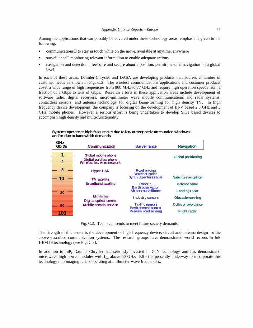
Appendix C. Site Reports—Europe 77
Among the applications that can possibly be covered under these technology areas, emphasis is given to thefollowing:
• communicationsto stay in touch while on the move, available at anytime, anywhere
• surveillancemonitoring relevant information to enable adequate actions
• navigation and detectionfeel safe and secure about a position, permit personal navigation on a globallevel
In each of these areas, Daimler-Chrysler and DASA are developing products that address a number ofcustomer needs as shown in Fig. C.2. The wireless communications applications and customer productscover a wide range of high frequencies from 800 MHz to 77 GHz and require high operation speeds from afraction of a Gbps to tens of Gbps. Research efforts in these application areas include development ofsoftware radio, digital receivers, micro-millimeter wave mobile communications and radar systems,contactless sensors, and antenna technology for digital beam-forming for high density TV. In highfrequency device development, the company is focusing on the development of III-V based 2.5 GHz and 5GHz mobile phones. However a serious effort is being undertaken to develop SiGe based devices toaccomplish high density and multi-functionality.
Systems operate at high frequencies due to low atmospheric attenuation windowsand/or due to bandwidth demands
GHzGbit/s Communication Surveillance Navigation
12
5
10
20
50
100
Global mobile phoneDigital cordless phone
Wireless loc. Area network
Hyper-LAN
TV satelliteBroadband satellite
MinilinksDigital optical comm.Mobile broadb. service
Road pricingWeather radar
Synth. Aperture radar
Robotic Earth observation
Airport surveillance
Industry sensors
Traffic sensorsEnvironment controlPreview road sensing
Global positioning
Satellite navigation
Defence radar
Landing radar
Obstacle warning
Collision avoidance
Flight radar
Fig. C.2. Technical trends to meet future society demands.
The strength of this center is the development of high-frequency device, circuit and antenna design for theabove described communication systems. The research groups have demonstrated world records in InPHEMTS technology (see Fig. C.3).
In addition to InP, Daimler-Chrysler has seriously invested in GaN technology and has demonstratedmicrowave high power modules with fmax above 50 GHz. Effort is presently underway to incorporate thistechnology into imaging radars operating at millimeter-wave frequencies.
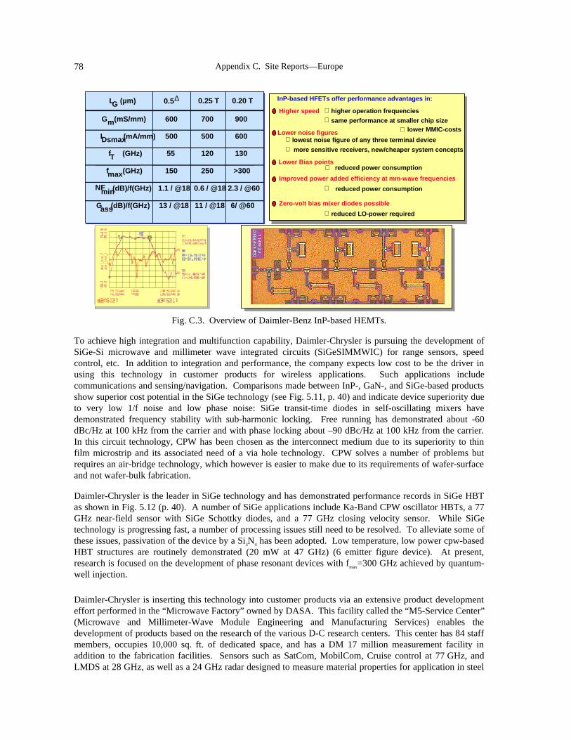
Appendix C. Site Reports—Europe78
LG (µm) 0.5 ∆ 0.25 T 0.20 T
Gm (mS/mm) 600 700 900
IDsmax (mA/mm) 500 500 600
fT (GHz) 55 120 130
fmax (GHz) 150 250 >300
NFmin (dB)/f(GHz) 1.1 / @18 0.6 / @18 2.3 / @60
Gass (dB)/f(GHz) 13 / @18 11 / @18 6/ @60
InP-based HFETs offer performance advantages in:
Higher speed
⇒ higher operation frequencies ⇒ same performance at smaller chip size
⇒ lower MMIC-costsLower noise figures⇒ lowest noise figure of any three terminal device⇒ more sensitive receivers, new/cheaper system concepts
Improved power added efficiency at mm-wave frequencies
⇒ reduced power consumption
Zero-volt bias mixer diodes possible
⇒ reduced LO-power required
Lower Bias points⇒ reduced power consumption
Fig. C.3. Overview of Daimler-Benz InP-based HEMTs.
To achieve high integration and multifunction capability, Daimler-Chrysler is pursuing the development ofSiGe-Si microwave and millimeter wave integrated circuits (SiGeSIMMWIC) for range sensors, speedcontrol, etc. In addition to integration and performance, the company expects low cost to be the driver inusing this technology in customer products for wireless applications. Such applications includecommunications and sensing/navigation. Comparisons made between InP-, GaN-, and SiGe-based productsshow superior cost potential in the SiGe technology (see Fig. 5.11, p. 40) and indicate device superiority dueto very low 1/f noise and low phase noise: SiGe transit-time diodes in self-oscillating mixers havedemonstrated frequency stability with sub-harmonic locking. Free running has demonstrated about -60dBc/Hz at 100 kHz from the carrier and with phase locking about –90 dBc/Hz at 100 kHz from the carrier.In this circuit technology, CPW has been chosen as the interconnect medium due to its superiority to thinfilm microstrip and its associated need of a via hole technology. CPW solves a number of problems butrequires an air-bridge technology, which however is easier to make due to its requirements of wafer-surfaceand not wafer-bulk fabrication.
Daimler-Chrysler is the leader in SiGe technology and has demonstrated performance records in SiGe HBTas shown in Fig. 5.12 (p. 40). A number of SiGe applications include Ka-Band CPW oscillator HBTs, a 77GHz near-field sensor with SiGe Schottky diodes, and a 77 GHz closing velocity sensor. While SiGetechnology is progressing fast, a number of processing issues still need to be resolved. To alleviate some ofthese issues, passivation of the device by a Si3N4 has been adopted. Low temperature, low power cpw-basedHBT structures are routinely demonstrated (20 mW at 47 GHz) (6 emitter figure device). At present,research is focused on the development of phase resonant devices with fmax=300 GHz achieved by quantum-well injection.
Daimler-Chrysler is inserting this technology into customer products via an extensive product developmenteffort performed in the “Microwave Factory” owned by DASA. This facility called the “M5-Service Center”(Microwave and Millimeter-Wave Module Engineering and Manufacturing Services) enables thedevelopment of products based on the research of the various D-C research centers. This center has 84 staffmembers, occupies 10,000 sq. ft. of dedicated space, and has a DM 17 million measurement facility inaddition to the fabrication facilities. Sensors such as SatCom, MobilCom, Cruise control at 77 GHz, andLMDS at 28 GHz, as well as a 24 GHz radar designed to measure material properties for application in steel

Appendix C. Site Reports—Europe 79
production, have been produced. Other products include a 58 GHz point-to-point link in hybrid formulationwith GaAs MMICs using bonding wires for connection to MMIC chips. This facility has been sole supplierto many communications companies (including Nokia) and focuses on defense/space products for guidanceand communications, with 60-70% in defense and 30-40% in commercial communications. The antennagroup of DASA does all antenna measurements.
In communications technology, Daimler-Chrysler is investing in telematics, advanced media and services,information technology, and software technology. Efforts are focused on application specific solutions for avariety of services including vehicle IT systems, personalized security systems, vehicle integration antennas,vehicle networks, multi-agent systems, and object oriented techniques. Other applications include thefollowing:
• Internet to the car by using flat panel displays
• Motiv: telemetric project to develop a traffic routing system using GSM (0.9-2.5 GHz)/DAB (1.8)
• Game: Global Automotive Mobile Entertainment
• error recording via Radio LAN
• digital radio via a short wave communication system (2-9.6 kB/s)
• mobile broadband communication systems (complementary of UMTS)
• 150 Mbps up to 5 km range wireless and mobile based on ATM
• ATM mobile (see above)
• fast train communications (38 GHz), among others
In addition to the above, Daimler-Chrysler is developing optical back planes for board-to-boardinterconnection. The back planes interconnect high-performance signal processors for modular avionics thatrequire 1-8 Gbps and require serial buses instead of parallel busses. The backplanes are designed in ring orstar configurations. Back planes offer advantages over space transmission since they provide a vibration-free solution. Free-space transmission and optical guidance through a polymer wave-guide give a 3 dB losswith an axial tolerance > 2mm and lateral tolerance better than +-500 micros. Power budgets are verycritical, and wave guide attenuation better than a few dB/m is required to make designs successful. Polymeroptical wave-guides with 1-3 dB/m attenuation in the short wave are used and are coupled through mirrorsfor good efficiency and low spillover. This technology has been demonstrated in a 1 Gb application. Thelength of the back plane was 26 cm and exhibited 3.5 dB loss. Demonstrated system margin wasapproximately 10 dB. Planar optical wave-guide crossing loss =0.7 dB, and line loss can be improved byanti-reflection coating. Total loss can be as low as 2.5 dB. An issue that needs to be addressed is thecollection of particles on the transitions of the optical wave-guide or on the lenses. Vibration tests haveshown excellent potential and aging tests of the low-loss wave-guide (200 hours) have indicated no increasein losses. Possible applications may provide 2.5 Gbps, while interconnection lengths up to 19 inches havebeen achieved.

Appendix C. Site Reports—Europe80
Site: Ericsson Radio Systems ABTorshamnsgatan 21-23164 80 StockholmSweden
Date Visited: 26 April 1999
WTEC Attendees: N. Moayeri (report author), A. Ephremides, M. Iskander, R. Rao, W. Stark, J. Winters,L. Young
Hosts: Soren Anderson, Manager, Antenna Systems and Propagation Research, EricssonResearch, Corporate Unit
Hakan Eriksson, Vice President and Gen. Manager, Ericsson Research, Corporate UnitHakan Eriksson, Manager, Radio Access Research, TerminalsUlf Forssen, Director, System and Technology, Business & Product Line Management
TDMA SystemsBjorn Gudmundson, Research Director, Radio SystemsBo Hedberg, Senior Expert, Radio Technology ResearchJohan Skold, Expert, Digital Radio Access in Cellular Systems, Radio Access and
Antenna Systems ResearchAnders Khullar, Ericsson, Lund
BACKGROUND
The panel visited the Radio Systems division of Ericsson, where most of the R&D work related to wirelesscommunications is carried out. Ericsson, however, is much more than this and is active in many other areasof electrical engineering and information technology. The most important and active area of wirelesscommunications from a commercial point of view, as the 21st century approaches, is the development of 3Gwireless communication systems. The International Telecommunication Union (ITU) is vigorously pursuingthe development of the International Mobile Telecommunication 2000 (IMT-2000) standard for 3G wirelesssystems, which it intended to complete by the end of 1999.
Ericsson is a powerful voice and a major player within the European Telecommunication Standards Institute(ETSI), which is the sponsor of the W-CDMA proposal for the IMT-2000 standard. Ericsson has had thelargest share and contribution in the development of Bluetooth, which is a short radio for wireless LAN typeapplications in the 2.4 GHz ISM band. To be more precise, Bluetooth is a cable replacement device thatconnects all personal computing and communications devices to each other in a wireless fashion. In fact, itis to be used even in future home appliances if all goes well with its development by Ericsson, IBM, Intel,Nokia, and Toshiba.
The first presentation was given by Hakan Eriksson, Vice President and General Manager of EricssonResearch, about the areas Ericsson is involved with and some facts about research in areas of hightechnology in Sweden. He said that universities are now more involved in industrial research in Sweden.They work closely with Ericsson. He then talked about the distinctions between 3G and 4G wirelesssystems. In case of 3G wireless, the spectrum had been clearly specified from the outset. It is much harderto define 4G wireless, because the spectrum has not been defined. He showed a slide of different wirelesssystems on a bit rate vs. mobility (fixed, local area, wide area) plane. He talked about three scenarios forvoice-over IP.
The first scenario is what we have today. He also compared several scenarios (cases of sending varioustypes of data) in traditional ways and over a wireless network. He showed that wireless made more sensethan the traditional ways in a number of cases, i.e., it was cheaper, at least with the present pricing structurewe have today. He also showed that for email, wireless is a lot better, but for images and video, traditional

Appendix C. Site Reports—Europe 81
ways are still better. He stated that it would be very unlikely that people would watch video on a smallpocket-sized terminal. However, such terminals would be good for voice, email, postcards, and music.
Bjorn Gudmundson explained that research at Ericsson has a shorter horizon than the 10 years that WTECstudy team member Tony Ephremides mentioned in his talk. Gudmundson added that the Ericsson staffpresent at the meeting all worked on radio aspects, and that they would not be the best people to answernetwork-related questions such as whether ATM or IP was the best alternative for sending voice and someother types of data over the network. There are some experts in those areas at Ericsson, but they were notpresent at the meeting. Regarding ACTS, FRAMES, and other such programs administered by the EC,Gudmundson said that he believed that those programs were not very efficient, as there is a lot of paperworkand overhead. On the positive side, these programs represent a framework for industry to work closer withuniversities all over Europe. But then Ericsson has had good informal relationships with the universities formany years.
Bo Hedberg gave a talk on multi-standard, multi-carrier, wideband radios. Multi-carrier radios have tohandle much larger dynamic ranges. That means stricter requirements on the A/D, D/A, and the multi-carrier power amplifier (MCPA). Some part of their architecture can be controlled digitally and throughsoftware. The RF front-end generally is not controllable. He said that power efficiency was important notjust at the mobiles but also at the base stations. Otherwise, they would have to use large fans to keep theMCPAs cool, and that would increase the price quite a bit. The dynamic range in multi-standard, multi-carrier, wideband radios would increase by about 20 dB over present systems (GSM). Half the cost of futurebase stations will be in the MCPA. The present price for this component is about $100 per watt of averageRF output power.
Hedberg felt that a lot of research was needed during the next several years to improve the MCPAs. Heconcentrated on the base station, because he thought the problem was harder for the terminal stations. Hefelt that the software radio solution was very costly for terminals. The technology needs to mature before itcan be used at terminals. Note that the multi-carrier requirements at the terminals are much looser than inthe base stations. The 1 microsecond frequency-hopping rate discussed refers to the radio at the base station.It is not possible to have such a high rate at the terminals. The present rate used at base stations, based onanalog synthesizer techniques, is one frequency hop per millisecond.
Soren Anderson gave a talk entitled, “Adaptive Antennas in Wireless Systems.” He outlined possiblealternatives for smart antennas and space-time processing. He presented a general radio architecture fortaking advantage of these concepts. As always, the interesting question is how much benefit would one getfor the cost? In cellular systems, the downlink is usually the bottleneck due to interference. So, when itcomes to smart antennas and space-time processing, it is best to concentrate on the downlink. In an FDDsystem, for example, one knows a lot more about the characteristics of fading in the uplink direction than inthe downlink direction. In a TDD system, one has a different situation.
Anderson then talked about the potential benefits of smart antennas in GSM downlink transmission. Heshowed a 5-6 dB improvement at the mobiles. Yet another example shows that with sector antennas thequality drops very quickly in comparison with smart antennas. The measure of quality was probability offrame error rate being less than 2%. Note that power control is independent of what was discussed here. PChas its own gains. Also note that to get the maximum benefit of smart antennas in a heterogeneous network,one needs to have good estimates of the traffic distribution in the cell.
Bjorn Gudmundson talked about radio access technologies. He said that mobile Internet access will be themain driver for wireless systems in the future. As far as fourth generation (4G) wireless is concerned, it isnot clear whether it should provide much better coverage-bitrate performance or somehow combine in anarchitecturally sound fashion a variety of systems such as LMDS, Bluetooth, WLAN, IMT-2000, mobilesatellite systems, etc. He then concentrated on the evolution of cellular systems by showing 2G, 2.5G, and3G systems. He put the EDGE system in the 3G category. He talked about the structure of dedicatedphysical channels in W-CDMA. He said that it was harder to use smart antennas in IS-95, because it

Appendix C. Site Reports—Europe82
handled the pilot bits differently than in W-CDMA. He then compared GSM and EDGE. In GSM themodulation is GMSK, which transmits one bit per symbol. EDGE uses 8 PSK. The concept of adaptivecoding and modulation helps EDGE adapt itself to the link quality. He went over major differences betweenW-CDMA and CDMA2000. He then talked about certain indoor systems (WLAN, Hiperlan-II, andBluetooth). The distinction between Bluetooth and HomeRF was questioned. Gudmundson did not haveany comments about HomeRF.
Ulf Forssen talked about EDGE and how it related to GSM and W-CDMA. It is, of course, an extension ofGSM. He discussed the relationships between EDGE, GSM, and TDMA/IS-136, as well as the tradeoffbetween spectrum efficiency and average throughputs. In summary, EDGE offers a way to harmonize GSMand IS-136. It has been approved by ETSI and UWCC and has been submitted to ITU. It will provideglobal roaming for a very large user base.
Johan Skold talked about W-CDMA. He went over a number of features of the UTRA system.
Hakan Eriksson, Manager of Radio Access Research, gave a presentation on mobile terminals. He talkedabout their present terminals and future directions. He also talked about some possible applications. Inaddition, he talked about Bluetooth and the Wireless Application Platform (WAP) Forum. Symbian(Ericsson, Nokia, Motorola, and Psion), which is an open architecture, allowing different softwaredevelopers to develop new applications for these terminals, was also discussed.
Anders Khullar’s talk was titled “GSM Terminal Evolution.” He discussed positioning systems and theirimpact on mobile price. He covered TOA, OTD, and GPS. He is with Ericsson, Lund.

Appendix C. Site Reports—Europe 83
Site: Filtronic PLCThe WaterfrontSalts Mill RoadSaltaire, ShipleyWest Yorkshire BD18 3TTUnited Kingdom
Date Visited: Friday, April 30, 1999
WTEC Attendees: D. Friday (report author), M. Iskander, T. Itoh, R. Rao, J. Winters
Hosts: Professor J. David Rhodes, Chairman, Filtronic plcProfessor Christopher M. Snowden, Director of Technology, Filtronic plcProfessor Peter Clarricoats, Chairman Technology Advisory Board, Filtronic plc and,
Chairman, Defense Scientific Advisory Council, Ministry of Defense, UKEric G. Hawthorn, Engineering Director, Filtronic ComtekDr. Richard G. Ranson, Director, Subsystems Engineering, Filtronic ComtekAlan Needle, Managing Director, Filtronic Comtek
Additional unidentified participants came and went throughout the day
FILTRONIC PLC, THE COMPANY
Filtronic was founded in 1977 and is a public limited company (plc) incorporated in England and Wales.Professor Rhodes has been Executive Chairman and Chief Executive Officer since its founding. Thecompany is multinational, with several subsidiaries in Europe, Australia, and North America, and it is aworld leader in the design and manufacture of a broad range of products for communication across the radio-frequency (RF) spectrum. These products include microwave and millimeter-wave devices, components andsubsystems for wireless communications, cellular handsets, components for hardwired networks such ascable TV and high-speed Internet access, and electronic warfare systems. The company claims to be able tosupply products at any frequency, for every transmission standard and every modulation system in the world.Its products primarily receive, transmit, filter, and amplify RF signals. Markets are categorized in four broadareas. These markets, and the percentages of Filtronic’s business in each of these areas in 1998, are asfollows: Wireless Infrastructure (55.8%), Cellular Handset (26.4%), Electronic Warfare (17.1%), and Cable(0.7%). In 1998, the company had sales of £181.1 million ($295.3 million), almost all its wireless businessbeing mobile cellular. The focus in this report will be on the commercial wireless communications aspectsof the business, the first two categories and 82.2% of Filtronic’s business.
In 1989, Filtronic bought Philcom Microwave, the first of its U.S. interests. This gave Filtronic atechnological edge with which to move, more rapidly, into the base station and mobile communicationsmarket. In 1994, the company went public on the London stock exchange. The commercial communicationsmarket is Filtronic’s primary customer base, and national-defense agencies form a second customer base.Filtronic supplies the latter with electronic warfare equipment and systems. The electronic warfare (EW)part of the business remains privately owned and provides access to the U.S. defense market. The advanceddefense technology, especially in communications, also provides Filtronic with a critical edge forcommercial applications. In the United Kingdom, Filtronic has facilities in Shipley (the CorporateHeadquarters and WTEC visit site), Stewarton, East Kilbride, Wolverhampton, and Milton Keynes. TheU.K. activities include the design and manufacture of wireless and cable products, EW products, and ceramicand ferrite wireless components. Filtronic has facilities (LK Products) in Kempele and Oulu, Finland, for thedesign and manufacture of access and subscriber products. In its Brisbane, Australia, facilities Filtronicdesigns and manufactures wireless and EW products. In the United States, the company has facilities in

Appendix C. Site Reports—Europe84
Salisbury Md., Merrimack, N.H., Santa Clara, Calif., and Natick, Mass. The more recent of these U.S.acquisitions include Litton Solid State, Sage Laboratories, and subsidiaries.
Primary commercial customers are the leading international original equipment manufacturers (OEMs).Filtronic plc employs approximately 3000 employees worldwide, including 250 engineers, of whom 10 %have Ph.D.s. Filtronic refers to its worldwide holdings and resources as the “Filtronic Group.” The Filtronicstrategic goal is to become the pre-eminent supplier of RF, microwave, and millimetric products.
FILTRONIC PLC, THE TECHNICAL PROGRAMS
Materials
Filtronic management, early on, saw materials as critical to competitiveness in wireless technology andacquired a U.K. ceramic and ferrite manufacturing company. The main materials-technology roadmap isfocused on requirements for ceramic resonators. The fundamental challenge is price vs. performance for thecomponents produced with these materials. Good performance means lower-losses (higher Q), higherdielectric constants (size reduction), and invariance of the material properties under changes in temperature.Present low-cost ceramic resonators have Q-values ranging from 15,000 to 20,000, and are based onceramics with dielectric constants ranging from 35 to 45. Current, high-end ceramics have dielectricconstants from 45 to 55 and achieve Q-values of 30,000. Filtronic representatives stated that one of thetargets was a resonator, at 1.96 GHz, with a loaded Q of 50,000. Their roadmap predicted high-Q resonatorswith dielectric constants ranging from 70 to 200 in 5 years.
Base Stations, Amplifiers, and Filters
Base station technology is another key element in Filtronic’s corporate planning and roadmapping efforts,with amplifier and filter performance the key issues. Dual-mode conductor loaded ceramic and high-Qcombline filters are mid-priced and also mid performance ( unloaded Qs of 5,000 to 8,000). TE (0,1,d) anddual-mode TE (0,1,d) filters achieve unloaded Qs of 50,000 but at twice the price. There is a need to dropthe price of these components. Filtronic is leveraging the Sage acquisition for base station couplertechnology. The wireline technology is low cost and yields high performance among competingtechnologies. Ferrite components and their manufacturing processes for planar circulators is another basestation technology the company is roadmapping.
Filtronic sees three viable options for base station filter technology for 3G: GPRS, EDGE, and W-CDMA.One option is modular systems including integrated systems, micro-controllers, and highly linear poweramplifiers. The second option is TE (0,1,d) ceramics technology including multimode, helical, and otherdesigns. The third option comprises improved versions of more traditional machined combline filters.Filtronic’s dual-mode conductor-loaded ceramic technology has enabled a one-half size reduction. Theinsertion loss is 0.5 to 1 dB for a typical base station. These devices have a very good Q (not given) and arethe result of an 18-month development period combining both ceramics technology and metalizationtechnology.
Filtronic does not have any projects for using high temperature superconductors (HTS) for base stationfilters. They cited the nonlinearities and reliability as factors that make HTS technology less attractive as aproduct line. Filtronic also believes that advances in conventional technology have marginalized theperformance gains of HTS hardware.
3G hardware will require improved linear amplifier technology and better efficiency, particularly forwideband CDMA. Software radio is doablethere should be no problems at the lower frequencies.Transceivers need to be cost effective. There is a need for distributed switching systems in base stations.One objective is to make a significant advancement (details unavailable) in Class A amplifier performanceby September 2000. Filtronic is taking an integrated approach, without close project management, and

Appendix C. Site Reports—Europe 85
researchers believe they have a key advantagespecial expertise and proprietary software for integration ofcomplex filters.
Base Station Antennas
Prof. Rhodes discussed the issue of the higher power (approximately 20 dB) needed for base stations to havethe same coverage for high data rate systems (such as EDGE) as for current mobile radio systems. Hediscussed the use of adaptive antennas, in particular, pencil beam phased arrays on the uplink and downlinkat base stations to provide a higher gain. Key research issues were seen to be multiband phased arrayantennas for base stations, along with filters and efficient and linear power amplifiers. Tower top electronicswere also seen as an issue. The use of terminal adaptive arrays was not felt to be practical (because of theexpense), as was the use of higher frequencies (because of diversity issues with point-to-point links). DSPpower was not felt to be a concern. Other Filtronic comments regarding base-station antennas were “wecan’t get away from pencil beams from the base stations,” and “multibeam RF is absolutely necessary anddifficult.”
Fixed Broadband Wireless
Comments concerning LMDS implied Filtronic does not see a wide market for this. Researchers said thatLMDS in the United Kingdom was licensed in the frequency band 40.5 to 43.5 GHz. Experimentsperformed led them to the conclusion that propagation reliability will be poor with the moist and rainyweather typical of the United Kingdom. They said that point-to-multipoint architectures were not likely tosucceed and that perhaps multipoint to multipoint would be a better architecture a dynamic network inwhich every user would be a possible relay-node. They didn’t see such an architecture being acceptable inthe more privacy and security conscious United States. They also feel that most demands can be met withexisting bands, and envision 1% of the market for LMDS, mostly wireless local loops. They also said one oftheir subsidiaries (Radiant Networks plc ) had a 25 Mbps wireless technology and that LMDS is not rightfrom either standpoint.
Wireless Handsets
The purchase of LK Products has extended Filtronic’s expertise and its market to include handsets.Customers now include Nokia, Ericsson, Siemens, Bosch, AT&T, Hyundai, etc. Clearly, the only directionshere are to make the handsets smaller, less costly, and more multifunctional and to improve theirperformance. Since handsets are simply housings for the real technology, the only solutions are in advancesin the components discussed elsewhere. Filters are a key component and in addition to the ceramictechnology discussed under “Materials,” surface acoustic wave (SAW) filters are showing promise. Helicalfilters, traditionally used in handsets, will likely drop out of use as ceramics and SAW improve. The oneexception is the handset antenna and integration of the antenna with its housing as well as the RF front end.Improved integration was seen as a key issue here. The cellular air interface also needs attention,particularly the antenna technology, the effects of hand placement, and the user-body effects on antennaperformance. Additional comments were “3G specifications, such as 2 Mbps are political issues,” “GSMwill be driven by power requirements,” and “multi-antenna handsets will be essential.”
Semiconductors
Filtronic does not use HEMTs but developed a capability (by acquisition) for fabricating pHEMTs. TheirpHEMTs have very high linearity, TOI up to 20 dB above P-sub-I. Researchers developed the capability forproducing MMICs up through mm-waves. Filtronic now has MBE and E-Beam capability, several class1000 and Class 100 Clean Rooms, and GaAs, InP, and YIG fabrication technology. Filtronic seessemiconductors as one of the most critical technologies, where it needs to maintain cutting-edge capabilitiesin design and manufacture, in order to remain competitive. The hosts had an interesting observation oncompeting semiconductor technologies particularly SiGe: They see the frequencies for Si technology beingpushed much higher and the costs for GaAs being pushed down. The end result is that SiGe technology will

Appendix C. Site Reports—Europe86
lose its perceived advantage and drop out as an alternative for wireless. The company has no SiGefabrication capabilities.
General Comments on Wireless Bands: Low Frequencies
Everyone will go to the limits to use these frequencies as much as possible. Some applications assumed tobe the domain of higher frequencies will be done in the future at lower frequencies, and industry willdevelop much more competence at exploiting these frequencies.
High Frequencies
Receiving much attention at present, but the ultimate applications and implementations will have to sortthemselves out. Many technical (hardware) challenges remain before this technology is competitive. Mostdemands can be met in the existing band.
SUMMARY/CONCLUSIONS
Filtronic Wireless Vision, Research Recommendations
Chairman Rhodes stated in his overview that the company’s technological niche requires that it operate inone of the world’s most highly competitive markets. Very rapid advances in technology characterize thismarket and its industries. Filtronic, he said, competes on the basis of cost, quality, performance, andmanufacturing and delivery deadlines. All R&D and corporate acquisitions are directed toward advancingthe technology, the expertise, and the production capability necessary to stay even with or ahead of thecompetition for the next major procurement contracts. If Filtronic falls behind, it will be adversely affected,and even its OEM customers may become competitors if they can manufacture equivalent products at lesscost. Filtronic has a long-term planning process and showed us for perusal (but did not provide) aproprietary copy of their strategic plans, the Filtronic corporate roadmap. Our perspective however, was thatthe technology requirements forecasting process was critically driven by the need to make the next logicalimprovement in existing devices, components, and subsystems. The rationale was clear. If the company’sproduct is not competitive in the next few rounds of procurement competition, the long-term future will beirrelevant. Although this essential aspect of the planning process was in the forefront, it was balanced by alonger term vision that encompassed new technologies, experimentation, and prediction of customers’ needsthrough the year 2005. Director of Technology Snowden stated that the horizon was only 5 years out, due tothe rapid evolution of markets and technology. William Smith, who spoke regarding the manufacturingoperations, said the basic mode of operation is “get the call today, deliver the product tomorrow.” A typicalproduct may go from specifications to a volume-manufactured product in less than eight weeks. This isclearly a very difficult environment in which to do long-term technology forecasting. However, Filtronic diddevelop and provide insights into the next steps in wireless hardware improvements.
The Filtronic management left the WTEC study team with its vision of the five key research topics that, overthe next five years, will have an important impact on future wireless communications technology products.The key topics are the following:
• systems perspective: systems architecture, hardware/software-integration/optimization
• smart antenna systems
• power amplifiers for both handsets and base stations
• filters (including materials)
• digital signal processing to enable more efficient use of hardware
Filtronic hosts stated that performance is the bottom line and given the success and rapid growth of Filtronicplc since its inception, this vision may not be too far off.

Appendix C. Site Reports—Europe 87
Site: GMD FOKUSGerman National Research Center for Information Technology,Research Institute for Open Communication SystemsKaiserin-Augusta-Allee 31D-10589 BerlinGermanyhttp://saturn.fokus.gmd.de/fokus/
Date Visited: 29 April 1999
WTEC Attendees: R. Rao (report author), A. Ephremides, N. Moayeri
Hosts: Eckhard Moeller, Head of Competence Center PLATINMihai Mateescu, Head of MOBRAChristian Schuler, member of MOBRA
SUMMARY
Forschungsinstitut für Offene Kommunikationssysteme (FOKUS) or the Research Institute for OpenCommunication Systems was formally established in 1988, but its roots can be traced to the much olderHahn-Meitner-Institut in Berlin. It had then and continues to have an institutional focus on providing“information at any time, at any place, in any form, and according to personal preferences.” GMD FOKUSundertakes research and pre-product development work on a variety of communications and computinginitiatives.
FOKUS draws 30% of its support from the German government. The remaining 70% comes fromcompanies like Deutsche Telekom and Textronix in Germany, Hitachi and NEC in Japan, the Racal DataGroup in the United States, from E.U. programs like ACTS and ESPRIT, and from national R&D programssuch as the German Research Network (DFN).
FOKUS takes part in a number of technological developments through R&D projects, management anddevelopment of international test beds, software and hardware prototypes, and product development.FOKUS is an active contributor to main standardization bodies such as OMG, EURESCOM, TINA-C, ATMForum, TMF, IETF, ETSI, ISO, and ITU-T, and is active, as well, in education at universities (in particularthe Technical University of Berlin) and other organizations. FOKUS has experience in developing workingdemos, and an essential part of its success in this regard comes from extensive industry involvement not onlyin donating equipment but also in setup and testing.
The organizational structure at GMD FOKUS and the funding mechanisms pursued exposes researchers tomarket forces. Although this exacts a price in the management of projects and recruitment and retention,research personnel seem to be engaged in relevant work.
About 20% of its 185 employees are permanent and the rest are hired for terms not exceeding five years.The permanent staff provides leadership and continuity. The temporary staff is hired for specific projectsand the duration of their appointments are directly tied to the duration of the projects. This is viewed as asource of some difficulty in hiring and retention.
Discussions with key senior personnel spanned issues pertaining to network centric and user centric supportfor mobility, hybrid fiber radios, scheduling for the wireless channel, error control, fourth generationsystems, cellular IP, and software radios.
Drs. Mateescu and Moeller, the WTEC panel’s gracious hosts at GMD FOKUS, believe that competition iskey to driving down the costs of access as well as the provision of proxy services to untethered mobile users.

Appendix C. Site Reports—Europe88
As far as mobility support was concerned, they saw particular merit in two architectures/technologies:architectures involving smart network resident agents that shadow mobile users and serve up appropriatelyreformatted information to low cost terminals and architectures where the mobile exercised more control andrelied on network infrastructure primarily as a low cost transport medium.
Dr. Mateescu believes that communication is about information exchange. Large databases will be used tostore this information, and therefore he sees high bandwidth optical networks as a key element of the overallcommunication infrastructure. In this context, an ongoing project on Hybrid Fibre Radio at GMD FOKUSwas described to the panelists. The system incorporates passive devices that convert optical signals to RFand vice versa. The architecture allows for the deployment of many low cost antenna/converter subsystemsthat are linked to a more central base station. EURESCOM (www.eurescom.de), a pan-European institutefor strategic studies in telecommunications, has an interest in understanding how this and other suchtechnologies would affect the business of European telephone service providers.
Although research driven by market forces has its appeal, Dr. Mateescu indicated that a new hurdle insecuring commitment of market actors for long-term projects was not the fear of failure but the fear that thework might become irrelevant in today’s rapidly changing environment. Senior leaders remain confidentthat through nimble management, the quality of the research at GMD FOKUS will remain high but someconcern was expressed about the quality of life of the researchers. An example of a long-term researchproject at GMD FOKUS within the confines of a standard was the development of packet “schedulingalgorithms over the RF channel.” This was viewed as a key point of differentiation between competingUMTS compliant data service providers.
GMD FOKUS was starting to explore “Fourth Generation” concepts in collaboration with major equipmentmanufacturers. At the current time, this new generation was viewed as extending the range and mobilitysupport for broadband wireless access. Investigations were also underway on the concept of “Secure CellularIP Networks.” Long-term research plans at GMD FOKUS include MAC, FEC/ARQ, software radio, HFR,radio independent access, and mobility routing. Applied research is focused on hardware/software prototypedevelopment, and GMD FOKUS does get involved in pre-product development through the creation ofnetworking software and software tools.
FOKUS ORGANIZATIONAL STRUCTURE
FOKUS was recently structured around nine centers of competence:
1. CATS, the Competence Center for Advanced Network Technologies and Systems, is focused on thedevelopment and implementation of new communication protocols, systems and services.
2. GLONE, the Competence Center for Global Networking, is focused on Internetworking services overvarious underlying technologies, enabling global communication, services procurement, and servicequality guarantees.
3. MAGIC, the Competence Center for Multimedia Applications for a Globally Interacting Community, isfocused on various aspects of interworking communication systems including issues of convergence.
4. PLATIN, the Competence Center for Distributed Object Technology, Platforms, and Services, aims tosupport new business opportunities that emerge from value-added, customized service provisions.
5. ECCO, the Electronic Commerce Competence Center, offers products, services, and consultation on thedesign, specification, and development of electronic commerce platforms and applications based onstate-of-the-art technology.
6. IMA, the Intelligent Mobile Agents Competence Center, offers services and consulting on the definition,specification, and development of agent platforms and applications based on state-of-the-art IntelligentMobile Agent technology.

Appendix C. Site Reports—Europe 89
7. MOBRA, The Competence Center for Mobile and Broadband Wireless Communications, pursuesadvanced R&D for protocols, interfaces, and applications of mobility in wideband/broadbandmultimedia networks.
8. TIP, the Competence Center for Testing, Interoperability and Performance, offers services andconsulting on analyzing, testing, measuring, and monitoring LAN and WAN components andapplications.
9. OKS, the Competence Center for Open Communication Systems, investigates technologies, platforms,and services to provide universal service access.

Appendix C. Site Reports—Europe90
Site: German National Research Center for Information Technologies (GMD)IPSIInstitute for Integrated Publication and Information SystemsDolivostrasse 15D-64293 DarmstadtGermany
Date Visited: 28 April 1999
WTEC Attendees: A. Ephremides (report author), R. Pickholtz, L. Katehi, T. Itoh, D. Friday
Hosts: Professor Dr. Wolfgang SchoenfeldMr. Matthias Hollick, GMD-IPSIMs. Nicole Berier, GMD-IPSIProfessor Dr. Ralf Steinmetz, Professor, GMD-IPSI and Technical University of
DarmstadtDr. Lars Wolf, Technical University of DarmstadtMs. Ana Pajares, Technical University of Darmstadt
BACKGROUND
GMD is the principal research organization of Germany that is primarily publicly funded and that focuses oninformation technology. Although detailed budget figures were not presented, a broad picture of GMD’sactivities emerged from the discussion. The organization is composed of eight institutes each of whichfocuses on separate (although interrelated) sectors of research activity. Four of these institutes are located inthe Bonn area (along with GMD’s headquarters); two are located in Berlin; and two in Darmstadt. IPSIfocuses on information distribution. As such it encompasses activities in the following:
• information management
• digital libraries
• information “publication” (in the broad sense of the term)
• future working environments
• mobile interactive media
• cooperative environments
The main activity of the institute that formed the basis of the discussion for the purposes of this study wasthat of mobile interactive media. As it emerged from the discussion, the main thrust of IPSI’s efforts in thisarea are focused on the upper networking layers (i.e., on the effects of mobility and of dynamicenvironments on network protocols) and not on the wireless medium per se.
There is close interaction between personnel at IPSI and the research staff (faculty and students) of theTechnical University of Darmstadt. In fact, at the WTEC meeting, representatives of both organizationsparticipated.
DISCUSSION
After the WTEC panel made a brief introduction and described the objectives of the study, ProfessorDr. Schoenfeld proceeded with an extensive review of IPSI’s programs on mobility issues. Later ProfessorDr. Steinmetz joined the meeting and complemented, with a brief commentary, the presentation ofDr. Schoenfeld. After lunch, Dr. Wolf described some additional projects that are jointly pursued by IPSIand the Technical University of Darmstadt. The meeting concluded with a broad discussion among all theparticipants.

Appendix C. Site Reports—Europe 91
The main focus of IPSI’s programs in mobility studies is on seamless roaming for interactive multimedia indynamic environments in which the logical connectivity among the hosts and the routers is changing. Assuch, it concentrates on the higher layers of the communication process.
As described by Dr. Schoenfeld, the objective of mobility tracking is to maintain consistent informationabout every node’s connectivity throughout the network. The networks of interest include WLANs, cellularnetworks, fixed wireless systems, and even systems with satellite links. When an end-node in a routing treechanges position, well-developed and well-understood methods of registration and reporting (from cellularnetworks) can be used. However, when intermediate nodes change position and connectivity, then themethod of “tunneling” can be used. This method has formed the basis of mobile IP and represents a short-term solution since the resulting new route is in general non-optimal. The long-term solution would have tobe based on rerouting. This is not easily accomplished in IP networks. Ongoing and future research on thisissue is addressing this problem.
In a sense, the search for improved solutions in this context suggests that routing in ad-hoc networks is animportant area that may have useful fallout in mobile computing. In fact, the DFN-Verein, which operatesthe network that interconnects universities and research institutes in Germany, maintains an interest inmobile computing and, through a new program, called MIRIAM, will permit IPSI to test the use or themodification of mobile IP as part of the research in adaptive routing.
A related problem that IPSI is investigating involves the continuous registration of a mobile host at a(possibly remote) home agent. The research concentrates on the theoretical modeling of this issue and on theresource management problem that arises when links that support different quality of service must bechosen. An E.U. project called COSMOS, in which IPSI is participating, addresses this issue. The role ofIPSI in this project, which assumes the use of satellite links as well, centers on middle-ware development.
Although IPSI recognizes the importance of the effects of the wireless link on the higher-layers (e.g., QoSvis-a-vis mobility), its primary concern is the development of upper-layer protocols that are compatible with,or are optimized for, dynamic topologies. By the same token, these upper-layer issues are cruciallyimportant and, yet, are usually ignored by the physical-layer community.
To handle environment changes, a service location protocol is needed and a classification of services isnecessary in order to determine which services should be provided at which location. In this regard, it wasclarified that location refers to the notion of topological connectivity and not of actual position coordinates(which is an objective of E-911 in the United States for future wireless services).
To assist in these projects, a Mobile Network Emulator is being developed that will actually include a linkpropagation model.
In response to a question from the panel, it was clarified that multicasting applications are not currently partof the focus in the IPSI projects.
The meeting, as mentioned earlier, included a description by Dr. Wolf, of the projects that are jointly studiedby the Technical University of Darmstadt and IPSI. These include a variety of topics that revolve aroundmultimedia networking from the point of view of content and information distribution. Some of these topicsare quality of service, heterogeneity, Internet telephony, security, gateways and protocols, contentprocessing, distance education, middle-ware, video servers, and content distribution. As the nature of thesetopics makes it clear that the emphasis is on general networking and not on wireless networking.Nonetheless, the relation to mobility (from the point of view of long-term mobility, i.e., the prediction ofneeds at different locations) renders this research relevant to wireless networking. Also, the issue of pricingof services, which in its own right has long-term implications for Internet networking as well as for wirelesscommunication, is on the research agenda of IPSI and the Technical University of Darmstadt.

Appendix C. Site Reports—Europe92
In the ensuing broadened discussion, in which the panel’s hosts were explicitly asked to address the long-term research issues and bottlenecks in wireless and mobile networking, it was mentioned that there is a2005 Master Plan for IPSI. This Master Plan encompasses the areas of media streams (includingentertainment services), ubiquitous computing, education, applications (such as telemedicine), andtechnology (e.g., security). Furthermore, it was pointed out that the ultimate bottleneck in networkcommunications would be the “usability” of the products and services, i.e., the needs and capabilities of theconsumer and user.
SUMMARY
The visit at IPSI highlighted issues in wireless networking that are often ignored by the wireless community,namely the need to address the design of upper-layer protocols and their effects on link operation. However,the WTEC panel visit verified that an integrated approach to networking that bridges gaps among layers isneeded but not yet in place.

Appendix C. Site Reports—Europe 93
Site: IBM Zurich LaboratoryCommunication Systems DepartmentSoodmattenstrasse 8H-8134 AdliswilSwitzerland
Date Visited: 29 April 1999
WTEC Attendees: T. Itoh (report author), D. Friday, L. Katehi, W. Stark
Hosts: Dr. Pierre R. Chevillat, Mgr. Wireless Communication SystemMr. Martin Hug
BACKGROUND
The panel visited IBM’s Zurich Research Laboratory in Switzerland and, more specifically, itsCommunication Systems Department, located in Adliswil in a suburb of Zurich. This building is severalkilometers from the main laboratory. It is planned for this building to be vacated shortly, as this departmentwill be relocated to the main site. This is one of eight research laboratories of IBM. The others are the T. J.Watson Research Center (headquarters), the Almaden Research Center, and the Austin Research Laboratoryin the United States. There are also research labs in Haifa, Israel; Tokyo, Japan; Beijing, China; and NewDelhi, India. The first three laboratories noted here employ 1,000, 800, and 220 people, respectively, whilethe other five laboratories each employ 200 workers. IBM Zurich has three departments: Science andTechnology (famous for the number of Nobel prizes awarded), Communication Systems, and AppliedComputer Science (formally IT Solutions). The two latter departments comprise the major part of theZurich operation.
SYNOPSIS
Mr. Martin Hug and Dr. Pierre Chevillat greeted the WTEC panel. After the welcome and presentation ofthe March 15 Workshop summary by the visiting panelists (T. Itoh, L. Katehi, W. Stark, and D. Friday),IBM researchers made four presentations and one presentation/demonstration. The first two presentationsand the presentation/demonstration came from the Communication Systems Department and are moreengineering oriented. They are (1) “Mobile ATM” by Doug Dykeman, Manager of IP and ATMNetworking, and (2) “Short-Range Radio Communication, HomeRF vs. Bluetooth” by Dietrich Maiwald,“Wireless Communication Systems,” and (3) “Infrared Technology” (Short Lecture and Demostration) byWalter Hirt, Wireless Communication systems. The remaining two were from Applied Computer ScienceDepartment. They are (4) “‘DEAPspace’ Short-Range Wireless Communication” by Dirk Husemann, ITSolutions, and (5) “Wireless Application Protocol (WAP)” by Carl Binding.
Fairly extensive discussions on the role of university research and on technical subjects have taken placeduring the technical sessions. The presentations are mostly software oriented. Little description was givenon hardware as it is outside of the charter and operation of these departments and are in some cases workedout at other facilities of IBM. The wireless subjects discussed were heavily oriented to data and computers.
MOBILE ATM
This project is for development of a mobile network integrated with a fixed infrastructure and is for aircraft,ships, and large ground vehicles. Uninterrupted operation is the goal while mobility is hidden from theusers. Key protocols are ATM and IP for voice and data in the range of 0 ~100 kbps. This is a mobile ad-hoc (reconfigurable) network.

Appendix C. Site Reports—Europe94
A new protocol called PNNI was introduced. PNNI routing has been accomplished while PNNI signaling isstill under investigation. ATM Forum Standardization is carried out, and the prototype implementation is inprogress with U.S. Navy through IBM’s U.S. operation. The Federated Battle Lab of the U.S. DoD (Army,Navy, and Air Force) and NATO are responsible for implementing the prototype, and a demonstration isplanned for September 1999.
Mobile IP, integration of IP on mobile ATM, and a new protocol for the future were discussed. Theproblems to be addressed are Routing (ATM, IP) and Re-routing (ATM). In the future, voice needs to beprioritized. Two problems that emerged from the discussions are the fading effect and frequency mobility(jamming in a military environment).
Short Range Radio (HomeRF vs. Bluetooth)
Because of the evolution of consumer electronics devices, connectivity is now a problem. Items in thiscategory include digital broadband (ISDN, LMDS, etc.), cellular phones, and PCCS in a changing life style.Interconnectivity should be built in, not created using many phone lines. The key to acceptance by thecustomer is that these devices be made “easy, affordable and standard.”
That is, the connection is interactive wireless without new wires. For Laptop and PDA, mobility isimportant. For the short-range format, Cordless (DECT) and Radio LAN, 2Mbps, 2.4 GHz includingHyperlan 1 (5.2 GHz, 10 Mbps) and Hyperlan 2 (5.2 GHz, 25 Mbps), are examples although simple infraredLAN has a problem in diffusion and shadowing by wall so that this can be used for line of sight only.
The following initiatives, HomeRF and Bluetooth, must be considered:
• HomeRF is in the unlicensed band. Ten companies are founding members, but the numbers extend to87. HomeRF is based on DECT frequency hopping, IEEE 802.11 at 2.4 GHz ISM band, 1.2 Mbpsfrequency hopping, 100 mW, range of up to 50 m.
• Bluetooth is a project started by five companies. Membership has expanded to 612. Specifications arenot firm, but a product was to appear in 1999. This system is based on a master/slave operation at 2.4GHz, 1 Mbps (1600 frequency hops). A single chip implementation is expected to cost less than $20.Ad hoc network capability will include up to three voice and seven data links. This architectureinvolves the replacement of cable, not a network. Applications include cable replacement, data accesspoint, and personal ad-hoc networks.
HomeRF is a networking project, but Bluetooth is for people on the move. The RF section was worked outat Yorktown. Future versions may use 5 GHz.
INFRARED TECHNOLOGY
IBM is working on advanced infrared wireless (AIr). Although similar physically to a TV remote control,AIr requires wide-angle (360°) coverage and long distance (10 m) data communication of 250 kbps to 4Mbps with an LED of 900 nm wavelength. An experimental demonstration was provided during the WTECvisit.
DEAPSPACE SHORT RANGE WIRELESS
This is a software project and the acronym came from Distributed Embedded Application Platform. Theobjective is to connect nomadic and pervasive devices through transient ad-hoc and proximity-based networkfor short-range (less than 10 m) applications. There is no master-slave arrangement but rather the devicesare allowed to talk to each other. The device characteristics are embedded into the microcontroller. There isno central node. Challenges for this software development are a description of services, flexibility andextensibility, simple process, and scalability. Currently, IBM has been working on simulation for transient

Appendix C. Site Reports—Europe 95
ad-hoc networks and primitive test beds. Some of the competition is SUN’s Jini, Microsoft’s Universal Plugand Play, and Xerox’s PARC’s UbiHome.
Support of Pervasive Application and Devices (Wireless Application Protocol or WAP)
This is an effort to develop an emerging industry standard for Internet style context to mobile users.Currently, 90 members are helping to develop such a standard. An example is EasySabre (airline reservationsystem with Web-like operation) where software translates html to WAP.
CONCLUSIONS
In the opinion of several WTEC panel members, this location understood the panel’s objectives most fully.IBM members, particularly the host, Dr. Chevillat, indicated their desires that the academy play an increasedrole in future oriented, often non-targeted research because most companies are decreasing researchoperations.
REFERENCES
White Paper “IBM Mobile ATM Networking Technology Overview.” Version 2, August 1998.
Gfeller, F., and W. Hirt. 1998. “A robust wireless infrared system with channel reciprocity.” IEEE CommunicationsMagazine 36 (12).

Appendix C. Site Reports—Europe96
Site: Institute of Mobile and Satellite Communication Techniques (IMST)(German name) Institut fur Mobil- Und Satellitenfunktechnik GmbHCarl-Friedrich-Gauss Strasse2D-47475 kamp-LintfortGermany
Date Visited: 26 April 1999
WTEC Attendees: Dennis Friday (report author), T. Itoh, L. Katehi, R. Pickholtz
Hosts: Prof. Dr. Ingo Wolff, President, IMST and Rector, Duisburg UniversityDr.-Ing. Mattthias Rittweger, Head of Department, RF Circuits and SystemsDipl.-Ing. Johannes Borkes, Head of Department, Integrated Circuits and SystemsDr. Ing. Dirk Heberling, Head of Department, AntennasWill Chr. Will Hildering, Head of Department, Systems
BACKGROUND
IMST provides central engineering, test, and development resources for the wireless, telecommunications,and information technology industries. Customers include almost all of the major European wireless andtelecommunication companies as well as companies throughout the Far East and Pacific, and Israel. Theintellectual resources at IMST include expertise in both the systems and the hardware aspects ofcommunications and information networks with a special focus on mobile wireless technology, bothterrestrial and satellite-based. Its wide-ranging technical programs include component and systemsengineering design, theoretical and experimental analyses, and special test and measurement services.
IMST President, Prof. Dr. Wolff, graciously served as the WTEC panel’s host. The people it primarilyinteracted with were the IMST equivalent of the board of directors, which included Dr. Wolff and all fourDepartment Heads. Dr. Wolff presented an overview of IMST, its history, its funding profile, itsorganizational structure, its technical programs, its staff profile, its customers, and its goals. His presentationwas followed by more program-specific presentations by two of the four Department Heads. They talkedabout wireless systems architectures, RF hardware design and performance, and antennas for wirelessapplications.
The formal presentations were efficient summaries of the relevant IMST programs, and were enriched withoff-the-viewgraph insights, peripheral discussions, and open and informative replies to the many questionsfrom the WTEC team. The two-way interaction was intense and they adapted their agenda accordingly, butthere was much more to discuss than the panel had time for, constrained by the need to travel from and toFrankfurt that day. Two of the department heads, with programs of interest to panel members did not giveformal presentations because of limited time, however they did participate in the discussions, and the panelwas given a condensed but comprehensive tour of the IMST laboratory facilities. Overall, the visit was veryproductive.
IMST, THE CORPORATE MISSION, HISTORY, AND ORGANIZATION
IMST management referred to the organization as a workbench facility for the wireless telecommunicationand information technology industries. Special focus is on mobile and microwave communicationstechniques for industrial applications, and much of the work is related to technology development andevaluation for next-generation personal cellular/mobile communications hardware and systems. Theireconomic niche is the gap between relevant cutting-edge research and industrial product development.IMST helps companies bridge this gap by partnering with industry and performing the generic research andengineering development work necessary to accelerate product development. This effort in turn reduces the

Appendix C. Site Reports—Europe 97
risk to industry in new commercial ventures. In addition to its primary role as a gateway between researchand commercialization, IMST provides a broad range of expert technical services to industry, performsmeasurements to characterize antennas and other components, develops and carries out specialized trainingprograms for industry, designs and fabricates special prototype hardware and software products for industry,and even carries out market research studies for new systems.
The institute is a private, non-profit corporation (designated GmbH in German). The laws governing a non-profit corporation in Germany are different from those in the United States. Most significant is the fact thatif a German company declares itself non-profit, at least 50% of its income must come from the government,or it will not be recognized as a non-profit organization and be taxed as a for-profit company. However,IMST, due to its special role as both a national resource and a key facility that will help the Duisberg regionattract high technology industries to compensate for their declining coal and steel industries, receives specialdispensation from this requirement. The IMST mission is to serve industry and to derive most of its fundingfrom the private sector. As a result of rapid growth in only a few years, and the excellent reputationacquired, approximately 80% of funding comes from the private sector, and 20% from publicly-funded R&Dprojects. Without special treatment as a non-profit company, IMST’s programs would suffer financially.Otherwise, IMST pays taxes like any other company. The success of IMST can be measured by steadygrowth ever since it was formed, to over DM10 million of business in 1999.
Dr. Wolff told us that he and the four other managers present at the meeting, and the Vice President, assumeall the technical and financial responsibilities for the operation of IMST. They pointed out that, unlike in theUnited States, the person who carries out all the legal work for the corporation is also an engineer bytraining. Professor Dr. Ingo Wolff’s commitment of time was especially significant since the panel learnedthat, in addition to his position as President of IMST, he had recently been appointed Rector of DuisburgUniversity (equivalent to chancellor of a university in the United States) and was embarking on a majorrestructuring within the university.
The IMST laboratories are located on a rural 10,000 m2 site a few kilometers across the Rhine fromDuisburg. The buildings contain 4,500 m2 of space, of which 1,500 m2 is laboratory space. The laboratoryspace includes a 300 m2 clean room and several electromagnetic anechoic chamber facilities for antennacharacterizations, electromagnetic compatibility measurements, and related wireless technology experiments.The building cost was DM12 million, and the total investment was DM17.5 million. Construction began in1992, and the institute began operation in January 1993. IMST presently has 87 employees from 15countries, including 68 engineers and scientists. IMST also maintains a close working relationship with theUniversity of Duisburg, and a total of 40 students work at IMST from there and from other universities.Staff size has been approximately constant since early 1996.
The organizational structure is straightforward, consisting of an administrative branch and four departments.Dr. Peter Waldow, Vice President of IMST, is responsible for operation of the company. He hasresponsibility for central services, marketing, legal issues, technology transfer and intellectual property,quality assurance, finances, and general administration. The four departments are Systems, IntegratedCircuits and Systems, RF Circuits and Systems, and Antennas & Electromagnetic Compatibility(EMC). Overviews were only given by the Systems and the Antennas and EMC Department Heads. Theothers were present throughout the meeting and participated in discussions.
The Systems Department, under the direction of Will Hildering, is responsible for communicationsnetworks and systems, satellite systems, wave propagation, mobile systems, signal processing, and digitalelectronics. The Antennas and EMC Department, under Dr. D. Heberling, is responsible for antennaperformance and characterization, EMC analysis and evaluation, and the interactions of human systems withelectromagnetic fields and wireless equipment. The RF Circuits and Systems Department, under Dr. M.Rittweger, is responsible for electromagnetic modeling and simulation of devices and circuits, the design anddevelopment of radio frequency (RF) circuits, modules, and printed wiring boards, and hybridmicroelectronics. The Integrated Circuits and Systems Department, under Dr. J. J. Borkes, is responsible for
Appendix C. Site Reports—Europe98
applications specific integrated circuits (ASICs), integrated communications circuits, RF circuits, and relatedmeasurement techniques. Only two of the departments provided overviews, and the division ofresponsibilities was not clear where there appeared to be an overlap.
IMST leverages its resources by partnering with industry, standards, and professional organizations. Theseinclude ETSI, the UMTS Forum, the UMTS Development Partnership, ITG, FGF, IMEC, IMAPS, theUniversity of Duisburg, and other groups. They also are ISO 9000 accredited and maintain an ISO 9001Quality System. They market worldwide by partnering with international technical marketing agencies.Customers include many of the key telecommunications companies in Europe and Asia.
IMST, THE TECHNICAL PROGRAMS
IMST is active in a broad range of technical programs focused on both the physical andarchitectural/algorithmic aspects of wireless systems communications. Emphasis is on mobilecommunications and 3rd Generation (3G) wireless technology. The role IMST plays in enhancing thedevelopment and competitiveness of European and Asian wireless technology is significant. IMST serves asa central laboratory resource for independent technology development, for reliable measurements, forimpartial performance evaluations, and for industry training and leadership. The main technical programswill be summarized in the following paragraphs.
Antennas and Antenna Characterizations
Antenna design and prototyping is one of the services provided by IMST. The activity in this area rangesfrom pure research for maintaining cutting-edge competence, to, for-contract, application designs, the lattercomprising mainly mobile radio antennas and microwave satellite communications antennas. Althoughantenna design was not a strong component of the briefings, the WTEC study team did visit some of therelated laboratories and see some prototypes. The antenna design challenges for handheld units were forinnovative designs fully integrated with the geometry and space-location constraints of the handset. Thedesigns also incorporated information gleaned from antenna-human interaction studies. There was alsosome work on integrated antenna-RF front ends. In addition to their design expertise, IMST researchers arevery strong in providing antenna characterization support for industry. Their antenna measurement facilitiesare of high quality and used for characterizing a broad range of antennas for both terrestrial and satellitecommunications. One is an indoor facility and the other is an outdoor range. The WTEC panel only visitedthe indoor range due to time limitations, but received a description of the outdoor range and viewed it from adistance.
The indoor antenna measurement laboratory is a totally shielded 8 x 12 x 5.5 meter facility used in twomodes, as a near-field facility and as a far-field facility. It is lined with pyramidal absorber and has a useablefrequency range from 400 MHz as a near-field facility (800 MHz as a far-field facility) to 50 GHz. Themeasurement apparatus is a 2.5 x 2.5 meter automated planar near-field scanner procured commercially. Asa near-field facility it is used primarily for determining pattern, polarization, and gain properties of high gainantennas used in satellite or long terrestrial links; and as a far-field facility, it is used for pattern andpolarization characterizations of electrically small, high frequency, low gain antennas used in hand-portableor vehicular-mobile telecommunications applications.
The outdoor facility is a standard far-field range with a 110 m separation and a 23 m source tower. The mainapplications are for characterizing pattern and polarization of physically larger and heavier antennas rangingfrom low frequency antennas down to 50 MHz, to high frequency, high gain antennas up to 18 GHz. Thereis also a mobile tower and a satellite-to-ground capability when longer baselines are required.

Appendix C. Site Reports—Europe 99
Studies of Human-Antenna Interactions
IMST also has an antenna program that focuses on the effects of the human user on the handset antennapattern, RF front-end and propagation, and also on the EM field patterns in the human body, particularly thehead. The latter is for evaluating and designing for compliance with European EM exposure regulations.IMST also has a well developed experimental and theoretical program for developing complete and realisticmodels of the electromagnetic fields inside the human body and around the human user of a mobiletelephone handset, as compared to the handset in isolation. The research includes developing accurateelectromagnetically equivalent models of the typical human body at frequencies of interest and performingaccurate measurements of field patterns.
IMST has unique experimental facilities dedicated to modeling the effects of the human body on air linkperformance. This work has several aspects. One is directed toward a standard measurement configurationfor comparing the performance of different handheld phones. A standard human replica artifact wasdeveloped by combining simple geometric forms into a circularly symmetric saline-filled standard humanresearchers call Charlie. The performance of different handheld units, both prototype and commercial, arestudied and compared by placing them adjacent to Charlie’s head and rotating Charlie in an anechoicchamber containing a receiving antenna that can scan vertically. The frequency range for this work is 10MHz to 6 GHz. IMST offers a service for determining realistic radiation characteristics and specificabsorption rates in the human body based on this model and is working with ETSI to standardize theprocedure.
Researchers also developed another facility for performing measurements to determine human-body effectson antenna and system performance and for use in modeling. The apparatus consists of a basin with asurface contour corresponding to the right half of the human torso, oriented vertically. The basin may thenbe filled with fluids that mimic the approximate electromagnetic properties of the human body at variousfrequencies. If a handset is placed under the basin near the ear, then this design enables the field patterns tobe measured inside the head, or elsewhere in the body for biological studies and for modeling effects onantenna performance. A precision computer controlled 6-axis robotic arm is used for precisely positioningelectromagnetic field probes on a spatial grid of points inside the fluid medium. The probes can measureboth the electric and magnetic near-fields of the transmitting antenna over a frequency range of 10 MHz to 3GHz in fluid and up to 6 GHz in air. This facility is called the Dosimetric Assessment System, or DASY.This facility is used for compliance tests for exposure limits as well as for optimizing new antenna designs.Software modeling services are provided that link with these measurements.
Environmental Reliability Validation
IMST also has a range of peripheral services for evaluating the reliability of the designs in normal use. Itprovides a sort of one-stop shopping lab for its customers’ essential needs. There are electrodynamic shakerfacilities and a time-variable-temperature chamber for testing components and systems under vibrational andthermal stress. Parameters such as voltage, current, frequency, power, spectrum (to 40 GHz), and bit errorrate are monitored during the environmental stress test to assess performance. Poor reliability can negateany superior electrical performance in a commercial wireless product. The facilities are set up specifically totest communications systems with coax and wave-guide connections to the unit under test.
Software Development and Services for Wireless Design and Modeling
IMST also performs the research and the software development necessary to produce and market a collectionof software packages for wireless design and modeling. One of the software products and services is a fullwave 3D FDTD PC program for solving Maxwell’s equations. Called Empire, it has special wireless-designoriented features for modeling RF microcircuitry as well as antenna performance and human body effects.There is also a software package for nonlinear modeling of FETs called TOPAS that has been incorporatedinto HP’s EEsof design and simulation software package. MEDEA is a system for the design of Silicon ICsincorporating thermal and electromagnetic constraints, while improving reliability and reducing costs.

Appendix C. Site Reports—Europe100
Coplan is a new design and simulation tool for design of coplanar waveguide (CPW) MMICs. It isintegrated with HPs EEsof and the user can perform simulations and optimization for GaAs designs up to 67GHz. Customers can purchase the packages, but IMST staff can also provide solutions for the customer, aswell as use the software for internal research.
Characterization of Active Wireless Components
IMST provides measurement services for a wide range of wireless and microwave technologies. IMST haswell-developed laboratory facilities for characterization of devices, circuits, and components. The differentmeasurement systems are used for internal research and development projects and are also used to providecomplete measurement services for external customers. Some of the systems and related software areoffered for sale. The total program provides a wide variety of measurement capabilities and services forboth linear and nonlinear characterizations.
The following is a summary of capabilities:
• fundamental linear characterizations
• scattering parameters: two- and three-port, 40 MHz to 110 GHz
• spectrum analysis
• thermal noise: 1 to 26.5 GHz
• noise figure: 100 MHz to 26.5 GHz
• phase noise
IMST has developed its own methodology and instrumentation for characterizing various nonlinearproperties of devices, circuits, and systems for one-port, two-port, and three-port configurations. Some ofthese capabilities are not commonly available and may incorporate unique analysis methods. This is also anactive research program for new techniques. These methods are available for on-wafer (coplanar geometry),microstrip, and coaxial lines. Unfortunately we did not see their microstrip measurement techniques.
The following are some of the specifications for harmonics and intermodulation products:
• load pull: 410 MHz to 110 Ghz, >80 dB dynamic range, > 10 W
• power sweep: up to 110 Ghz, > 10 W, VNA analysis
Electromagnetic Compatibility Design and Assessment
IMST has extensive expertise in both modeling and measurements for characterizing electromagneticcompatibility of radio/wireless products. Modeling software and experimental facilities include an anechoicchamber. These capabilities are used to perform research, as well as to provide customers with data and withtest services to determine whether product emissions satisfy U.S., international, and E.U. trade complianceregulations. IMST is on the U.S. FCC list of approved facilities for certification of specific absorption ratefor handheld products headed for the U.S. market. EMC compliance of all electronics/wireless products andofficial recognition of test facilities are significant issues in wireless for the global market.
Design and Prototyping
IMST provides services for design and prototyping of RF devices and RF front-ends. Excellent RF designsoftware is available, both in-house developed and commercially available software. Capabilities includeCAD, simulation, optimization, and EM field simulation for RFICs, MMICs, ASICs, hybrids, andcommunication systems. It has complete clean room and GaAs fabrication facilities (300 sq. m - class 100to 10,000) for developing prototype devices and systems. IMST is very active in this area. Some of theprojects include the following:

Appendix C. Site Reports—Europe 101
• new, more efficient devices and microcircuit geometries (layered, etc.)
• RF front ends for handsets
• RF modules for communications transcievers
• complete radio systems including a software radio that was really an RF front end with a softwarereconfigurable digital/systems section
Overall this effort comprised a significant portion of the activity, and IMST demonstrated a successfulhistory of having designed and developed the RF sections, and other components, for many successful radioproducts manufactured by well-known international electronics/wireless companies in both Asia and Europe.
SUMMARY/CONCLUSIONS
IMST is, by its mission, and the work it engages in, forward looking. The projects all reflect the cutting-edge technology for commercial products. IMST’s brief history combined with its growth and successesspeaks for its capabilities. In short, IMST appears to be well embedded in the enabling technologiesunderlying the worldwide wireless industry, and its management and technical staff are competent and in agood position to observe major trends and assess emerging technologies. Programs address importantproblems in the wireless industry. For example, in addition to GSM refinements, IMST is active in UMTS,DECT, and general 3G and 4G issues. The current focus, with the exception of satellite technology, isalmost totally terrestrial, portable, and mobile.
IMST sees the wireless industry evolving as essentially mobile technology embedded in adaptivearchitectures and believes that the mobile economy will expand astronomically. IMST researchers statedthat Europe is not interested in LMDS for Europe, just as a possible product to sell abroad wherever it ismarketable. As a result, it is not receiving much attention and no energy is being expended in this area withrespect to standards activities or R&D as happened on GSM or is now happening on UMTS. No onebelieves that a market exists in western Europe for LMDS systems or services in western Europe, becausethere is already a hard-wired infrastructure that will meet all European needs. IMST researchers also aren’tconvinced that the performance of broadband wireless systems at 30 MHz frequencies will be superior towired broadband systems or to advanced mobile systems.
The broad but focused range of programs covers virtually all hardware aspects of wireless. Many of thedesigns exhibited were straightforward but well executed. Other designs reflected innovation andexperimentation. The centralized wireless-focused design, device prototyping, software services, test andmeasurement services, and products provided are clearly an asset to customers, and enhancecompetitiveness. While the WTEC panel saw no great departures from conventional technology, IMST is akey facility and a lab to watch. Two examples of programs that best reflect cutting edge thinking andplanning are the nonlinear circuit and device modeling and characterization project and the elaboratetheoretical and experimental program to assess the interactions of the handset antenna and the human userand model the effects on propagation, RF circuitry, and field levels in the body. The significance of theseprojects is the contributions they will make to aspects of wireless design that are presently only partiallycharacterized. Devices in handheld units are always operating in or near saturation to optimize battery lifeand the design process to optimize the nonlinear behavior is a black art. Propagation paths can degrade 3 to5 dB when the typical GSM phone is placed near the head, and other wireless units have exhibited 8 to 10dB degradation in the hands of users. These are important programs and important wireless issues.

Appendix C. Site Reports—Europe102
Site: NokiaP.O. Box 4500211 HelsinkiFinland
Date Visited: 27 April 1999
WTEC Attendees: W. Stark (report author), N. Moayeri, R. Rao, J. Winters, A. Ephremides, L. Young,M. Iskander
Hosts: Heikki Huomo, Vice President, Research and Technology Product CreationYrjo NeuvoAntti Yla-Jaaski
BACKGROUND
Nokia is a leading manufacturer of wireless communication equipment, including cellular phones and basestations. Nokia has research facilities across the world including Helsinki and Richardson, Texas. Nokiarevenue has been increasing at a rate of roughly 30-35% per year for the last 15 years. Nokia has led theindustry in marketing phones. Nokia has hired outside companies for research including TI for research onsolid state devices. Nokia spends about 8% of sales on research and development. Not all of this wasinternal research as Nokia sponsors research by other companies and universities. Nokia has 44,543employees in 45 different countries with research centers in four countries.
The meeting at Nokia began with a fairly large group (around 30) of engineers, product developers. Theseengineers were participating in a continuing education program whereby Nokia brings in experts fromuniversities together with Nokia engineers. Nokia has a formal mentoring type of program for engineers inorder to continue their professional development. This may be quite unique compared to many othercompanies.
The meeting had several parts. First, Prof. Ephremides, chair of the WTEC panel, gave an overview of thegoals of the study and sponsorship. Second, two members of the Nokia research staff, Hekki Huomo andAntti Yla-Jaaski made presentations, followed by discussion and questions from the panelists. After this, alunch meeting with Hekki Huomo and Antti Yla-Jaaski was held, where further discussion regardingresearch took place.
At the first part of the meeting, research areas of interest to the panel relevant to wireless communicationswere discussed. Dr. Neuvo of Nokia added display technology and EMC effects to the list of importantresearch areas.
Dr. Huomo discussed the generations of wireless systems from first generation AMPS/NMT to thirdgeneration, from analog modulation to digital modulation. The second to third generation is from mainlyvoice to a combination of data and voice along with packet oriented services.
He also discussed wireless computing where the data rate is from 2-155 Mbps, the carrier frequency is muchhigher (2GHz and above), and the service is best effort. The architecture of the network is also not celluar/hierarchical. The future drivers for wireless communication include multimedia communications. A newway of presenting information is needed. The Internet was a success because of available content withintuitive access. A means of differentiating between personal data and work-related data was also discussedas a future goal. Data would be gathered, in this scenario, depending on whether the user is at home or in theoffice.

Appendix C. Site Reports—Europe 103
It was suggested that service and protocols will have more influence in the future and that the driver oftechnologies will be service and application protocols and not more capacity (as is the current driver).
The following list of technologies needed to achieve these applications was suggested:
• board assembly/packaging
• chip scale packaging
• RF passive integration with MCM-D
• flip chip technology
• filer integration with BAW
• CMOS RF
• enhanced digital and analog ASICs (Productivity in ASIC design must grow so that a Pentium can
be designed in one man-year)
• product architectures
• mechanics
• user interface
• external interfaces
• antennas
• battery and energy management
• software defined radios (SWDR)
• technology to create multimode and multiband radios
• technology to create mobile multimedia platforms
• radios that are flexible and easily configurable
• Software or quick design cycles
• radios based on virtual components
SUMMARY
Nokia is a very product oriented company with a heavy emphasis on marketing cellular phones. It hasbecome an international company, leading the industry in cellular phones, and is focusing on systemsintegration. Nokia has a unique system for mentoring employees with university faculty. The researchdrivers for future wireless communications include high speed, high frequency transmission of multimediadata, and personalizing data retrieval. The research topics needed to achieve this include boardassembly/packaging, chip scale packaging, RF passive integration with MCM-D, flip chip technology, filerintegration with BAW, CMOS RF, enhanced digital and analog ASICs, user interfaces, external interfaces,antennas, and battery and energy management.

Appendix C. Site Reports—Europe104
Site: Philips Research LaboratoriesProf. Holstaan 45656 AA EindhovenThe Netherlandshttp://www.research.philips.com/generalinfo/laboratories/netherlands.html
Date Visited: 28 April 1999
WTEC Attendees: J. Winters (report author), M. Iskander, N. Moayeri, R. Rao, W. Stark, L. Young
Hosts: Dr. C.P.M.J. (Stan) Baggen, Research Fellow, Digital Signal ProcessingDr. H.A. (Rick) Harwig, Director, Electronic SystemsDr. Peter Baltus, Research Scientist, Integrated TransceiversDr. Marcel J.M. Pelgrom, Department Head, Mixed Signal Circuits and SystemsDr. Paul Kaufholz, Research Scientist, User-System Interaction TechnologyProf. Dr. J.W. (Hans) Hofstraat, Department Head, Polymers & Organic ChemistryDr. Jean-Paul M.G. Linnartz, Senior Scientist, Broadband Communications &Video
SystemsDr. Carel-Jan L. van Driel, Department Head, Digital Signal Processing GroupDr. C.R. de Graaf, Senior System Architect, Compact Personal Communicator
BACKGROUND
Royal Philips Electronics is one of the world’s biggest electronics companies and Europe’s largest, withsales of $33.9 billion in 1998. Founded in 1891 in Eindhoven, the Netherlands, it is a global leader in colortelevision sets, lighting, electric razors, color picture tubes for televisions and monitors, and one-chip TVproducts. Its 233,700 employees, in more than 60 countries, are active in the areas of lighting, consumerelectronics, domestic appliances, components, semiconductors, medical systems, business electronics, and ITservices. The WTEC panel visited Philips Research Laboratories in Eindhoven.
Philips Research was started in 1914, and currently has 3,000 employees worldwide, with 1,700 employeesin the headquarters in Eindhoven. The major research areas are materials (29%), electronics (15%), andsoftware, systems and devices with a budget of $600 million for research out of an R&D budget of$2.2 billion. Over 60,000 patents have been issued to Philips Research, which is the backbone for corporatetechnology strategy.
Rick Harwig, Director of Electronic Systems, gave an overview of the work at Philips ResearchLaboratories, describing the various projects and achievements that have been made. He noted that there arecurrently 150-200 people involved in wireless, and the number is expanding at a slow rate, due to the lack ofqualified candidates.
RESEARCH AND DEVELOPMENT ACTIVITIES
The panel heard six technical talks on research projects at Philips Research Laboratories. Peter Baltus,Research Scientist, discussed RF front ends for wireless communications. He first noted the trend to higherdata rates and frequencies, with outdoors up to 5 GHz and indoors greater than 10 GHz for higherbandwidths. He saw the main issues for RF electronics as lower cost, low weight and volume, and longtalk/standby time.
Noting that the RF front end consumes more than 50% of the total power in a handset and currently usesmore than 20 external components, he stated that the main challenges are the integration of the transmitter,integration of the antenna interface, multiband/multimode operation, and A/D technology. This includes

Appendix C. Site Reports—Europe 105
eliminating external impedance matching circuits and duplexer components, along with advanced antennadiversity. Since Philips is primarily involved in handsets (e.g., in DECT), the main emphasis of thediscussion was on techniques for handsets. Baltus described the Philips scanning dual-antenna handset,noting the need for better radio channel characterization. He then stated that one method for powerreduction was the elimination of the substrate to get around parasitics’ problems and discussed PhilipsSilicon-on-Anything technology and how this technology could be used to integrate high Q resonators.
Marcel Pelgrom, Department Head, Mixed Signal Circuits and Systems, discussed A/D conversion andpower management for future digital systems. He noted the tradeoff of resolution versus bandwidth in A/Dconverters, which results in large power at high resolution and bandwidth. The challenge is to achievehigh-speed/resolution A/Ds so that multichannel transceivers can be integrated for lower cost. The trend inhigher resolution/bandwidth A/D converters was seen to be continuing for another 6 to 10 years, with3 orders of magnitude improvement still left. This should result in practical A/D converters for WCDMA in4-5 years. In power management, the trend in increasing energy per weight and size was seen through theevolution of batteries from NiCd to Li-ion to Li-poly to future unknown materials.
Interestingly, one of the best research areas for power management was seen to be in better powermanagement software, including improved protocols. It was stated, however, as in the previous talk, that RFpower will dominate over software power, and additional digital signal processing (DSP) will notcompensate for poor A/Ds. Thus, he felt that long-term research should emphasize RF and packagingresearch over DSP/software improvement, although software improvement can have some effect on RFdesign.
Paul Kaufholz, Research Scientist, User-System Interaction Technology, discussed voice control in theliving room. He noted that with more wireless devices in the future, there would be a growing need forbetter user interfaces to these devices, in particular, voice control. The key challenges were seen to beacoustic speech recognition and echo cancellation.
Hans Hofstraat, Department Head, Polymers & Organic Chemistry, discussed polymers: new options forelectronics. With polymers, the main advantage is very low cost. Currently, polymers are used for LEDstoday, and he demonstrated such a device. In 2-3 years they should be used in electronics, and in 5-10 yearsin batteries. This has the potential to reduce costs to the point that disposable wireless phones may befeasible. However, substantial research is still needed, with particular emphasis on multidisciplinaryresearch, which is a challenge.
Jean-Paul Linnartz, Senior Scientist, Broadband Communications & Video Systems, discussed wirelesssystem issues. In particular, he felt that as higher data rates stretched the limits of bandwidth, wireless datasystems would evolve to a frequency reuse of 1 (frequency reuse in every cell). With this reuse incombination with dynamic channel assignment, research was needed into channel assignment with datapackets, i.e., dynamic packet assignment. He also stated that there should not be one system to handle bothshort messages and high data rate services such as HDTV, but a combination of systems. Furthermore, forhigher data rate systems the trend may be away from spread spectrum type of systems.
C.R. de Graaf, Senior System Architect, Compact Personal Communicator, discussed ultrawide bandwidthsystems and briefly described the possibility of placing the transceiver on a chip.
After the presentations by Philips, Ramesh Rao presented the results of our national workshop to a seminargroup of about 50 Philips employees. There were discussions with the group covering the above areas,including discussions on ultrawide bandwidth systems.
REFERENCES
Philips Research Brochure, “Science emanates not just from the mind, but also from the heart.”

Appendix C. Site Reports—Europe106
Mosaic of Philips Research, Number 5, 1998.
Baltus, Peter. “RF front ends for wireless communications.” viewgraphs.
Kaufholz, Paul. “Voice control in the living room.” viewgraphs.
Hofstraat, Hans. “Polymers: new options for electronics.” viewgraphs.

107
APPENDIX D. SITE REPORTS—JAPAN
Site: Advanced Telecommunications Research-International (ATR-I)2-2 HikaridaiSeika-cho, Soraku-gunKyoto 619-0288Japan
Date Visited: 31 May 1999
WTEC Attendees: A. Ephremides (report author), R. Pickholtz, R. Rao, J. Maurice, B. Mooney
Hosts: Dr. Bokuji Komiyama, PresidentDr. Nagao OginoMr. Keizo InagakiMr.Yuichiro Ohno
BACKGROUND
ATR is an institute/laboratory established in 1986 as a joint organization. Each laboratory receives 70% ofits support from Japan’s Key Technology Center (Key Tec) and 30% from private companies, whosemission is to engage in high risk, basic research ventures in the broad field of communications.
Its mode of operation is fairly unique in that it is based on externally approved, seven-year projects that aremanned with personnel mostly borrowed from participating companies.
The WTEC panel visited only one of the current four seven-year projects (referred to as laboratories withinATR). This laboratory, called the ATR Adaptive Communication Research Laboratories, was established in1996 and is currently operating with a budget of ¥11.9 billion for the period 1996-2003.
The other three (established respectively in 1995, 1993, and 1992) are the ATR Media Integration andCommunications Research Labs, the ATR Interpreting Telecommunications Research Labs, and the ATRHuman Information Processing Research Labs.
When its seven-year cycle expires, a project may be continued if its goals are not yet fully accomplished or itmay be discontinued if it has fully achieved these goals. The goals consist of patenting and commercializingthe products of the research effort. The term used within the organization for the latter is managing the fruitsof research. Currently, there are four such successfully completed projects.
The overall annual budget for all four operating laboratories is currently ¥7.4 billion.
DISCUSSION
The WTEC panel visit commenced with a round-table welcome and introduction by Dr. B. Komiyama, thePresident of the ATR Adaptive Communications Research Labs. As explained by Dr. Komiyama, the Labsconsist, in turn, of four departments. There is one department on Architecture for AdaptiveCommunications, one on Design and Control of Adaptive Systems, one on Advanced WirelessCommunications, and one on Advanced Communication Devices.
Dr. Komiyama had selected four projects to brief the panelists in detail. Two of these are in the departmentof Architecture for Adaptive Communications and focus on upper-layer issues and the other two are in the

Appendix D. Site Reports—Japan108
department of Advanced Wireless Communications and focus on lower-layer issues. Specifically, theformer two include self-organizing wireless networks and adaptive QoS management, and the latter twoinclude microwave photonics and intelligent antenna arrays.
The briefings on these projects were conducted by the respective directors or principal investigators and tookplace within the specific lab environment of each project. All were explained in detail and wereaccompanied by demonstrations.
Self-Organizing Wireless Networks
This project focuses on the development of an ad-hoc, flat network with adaptive topology control. Theultimate objective is to test topology control algorithms on a real testbed and to include routing and media-access-control (MAC) provisions. In addition, the algorithms are envisioned to operate in distributedfashion. For the moment, the emphasis is on centralized algorithms and limited to logical connectivitycontrol (clustering). The main idea is to adjust the clusters based on the changing traffic conditions.Presently, the investigators are using genetic algorithms as the basis for such topology control. The intendedapplications include stadium events or other similar gatherings of large numbers of users.
Adaptive QoS Management
The objectives of this project are to develop adaptive ways in which application-level QoS is controlled inresponse to changing environments in multimedia applications. The current focus is on controlling thecompression and transmission parameters of video streams (bit-rate, frame-rate, etc.) through negotiationamong network agents that correspond to the different user streams. It is later expected that thesenegotiations will include allocation of additional network resources (such as buffer memory, bandwidth,etc.). The investigators do realize that end-to-end QoS performance depends on lower-layer (link) QoSparameters and intend to include this coupling into their methods. At the time of the site visit, there wasfocus on the use of motion-JPEG because of its scalability. Thus, other stream formats are converted tomotion-JPEG before the adaptive negotiations are performed.
Microwave Photonics
The goal of the project is an imaginative use of optical signal processing for adaptive antenna arrayapplications. Unfortunately, the speed and complexity of the needed FFT computations limit mostalgorithms for beam forming. This project proposes to convert the microwave signals up to infrared opticalbands, perform the FFTs through a lens (essentially instantaneously), and then convert the signal back downto its natural carrier frequency. The multitude of problems associated with this idea, laser frequencystability, non-reciprocal structures at transmitter and receiver for the up and down conversions, and theelectro-optical integration, are currently being addressed. This project is an excellent instantiation ofintegration across layers in wireless networking. In this case, the hardware, the beam forming, and the signalprocessing are all coupled in a unified design approach.
Intelligent Antenna Arrays
This project is close to current mainstream research that is geared toward multi-user CDMA applications. Itfocuses on beam forming and tracking for both narrow-band and wideband cases for the simultaneousreception of several signals. Constant Modulus Algorithm (CMA) techniques, that are blind, as well asrecursive tracking techniques (based on Kalman filtering) are used; and experiments are conducted with 44-tap transversal filters, 16 or 32 antenna elements, and simultaneous operation of 4 beams. The difficulty ofmulti-beam A-to-D conversion (in terms of needed processing bandwidth) is recognized and will beaddressed.

Appendix D. Site Reports—Japan 109
CONCLUSIONS
True to the stated mission, these labs are focusing on long-term research. The technologies they are focusingon include the challenging one of ad-hoc networking and are illustrating a visionary integrated approachacross layers. They also reflect perfectly the perceived need for spatial diversity, hardware/softwareintegration, and coupling of QoS to lower layer networking issues.

Appendix D. Site Reports—Japan110
Site: Fujitsu Laboratories4-1-1 Kamikodanaka, Nakahara-kuKawasaki 211-8588Japan
Date Visited: 3 June 1999
WTEC Attendees: N. Moayeri (report author), A. Ephremides, B. Mooney, H. Morishita, R. Rao, W.Stark
Hosts: Jifeng Li, Researcher, Wireless Communication Systems Laboratory, NetworkSystems Laboratories
Tamio Saito, Senior Researcher, Wireless Communication Systems Laboratory,Network Systems Laboratories
Yukio Takeda, Director, Wireless Communication Systems Laboratory, NetworkSystems Laboratories
INTRODUCTION
Dr. Takeda started the meeting at 9:35 a.m. and went over the agenda for the meeting. Dr. Ephremides thenoutlined the WTEC panel goals for the visit.
Dr. Takeda gave the first Fujitsu talk on the organization of Fujitsu Laboratories, Ltd., which was establishedin 1968, has about 1,500 employees, and has capital of ¥5 billion. He discussed Fujitsu, Ltd., which wasfounded in 1935, has over 180,000 employees, and had consolidated revenues of $44 billion in the fiscalyear, which ended in March 1999.
RESEARCH AND DEVELOPMENT
Dr. Takeda discussed the Wireless Communication Systems Laboratory, which consists of 25 employees andwhich he is in charge of. The laboratory is concentrating on 3G and 4G wireless systems and IntelligentTransportation Systems (ITS). In 3G and 4G the researchers are investigating interference cancellation usingmultiuser detection and adaptive array antennas for W-CDMA base stations. He showed a picture of twohardware racks researchers have developed to study the two approaches mentioned above. These weredeveloped in collaboration with FTRC. In the ITS area researchers are developing a millimeter wave radar.
Dr. Saito presented a talk on interference cancellation and mobile multimedia communications. He talkedabout the drastic increase in the number of wireless communication users in Japan. Two data services arecurrently offered in Japan, a 28.8 kbps service for PDC users and a 64 kbps service for PHS users. Theinterference cancellation scheme is a two-stage system, followed by a RAKE receiver. This system results in1.6 Db performance improvement at a BER of 10(-3). This results in an almost doubling of system capacity.However, in practice in a multi-cell system, the capacity improvement is only 1.3. In the practical systemthe interference cancellation scheme is applied to high rate data users, because they transmit at higherpowers. Multiuser detection is also employed. The system can cancel a maximum of 32 interferers.
In the second part of his talk, Dr. Saito described the Multimedia Mobile Access Communications PromotionCouncil (MMAC-PC) and its collaborations with IEEE 802.11B and ETSI BRAN. Fujitsu is consideringtwo systems, one with a bit rate of 6-10 Mbps (with a maximum of 25 Mbps) in the 25/40/60 GHz band andanother with a bit rate of 156 Mbps in the 60 GHz band. These systems are for stationary or slow movingusers. He gave some details on the physical link aspects of these two systems and mentioned that the workon the MAC layer is underway.

Appendix D. Site Reports—Japan 111
Next Dr. Li described turbo coding for W-CDMA, which Fujitsu is proposing to standardization bodies suchas ARIB and ETSI and recently within 3GPP. Turbo coding is used for higher data rate modes of W-CDMAand possibly CDMA2000. He went over a Fujitsu puncturing method for turbo codes and compared it withanother one proposed by the Korean company LOGIC. The Fujitsu approach was slightly better at highersignal-to-noise ratios. In addition, it was simpler to implement.
He then described a multidimensional turbo-coding scheme, which used three decoders in each iteration. Heshowed the performance of this coding scheme when used in conjunction with W-CDMA over the FPLMTSVehicular B channel model. It shows improvements over the conventional turbo coding method.
He then briefly talked about interleaver design for turbo coding, specifically a modified symmetricS-interleaver. In the discussion following Li’s presentation, the issue of the tradeoff between degree ofspreading and the coding rate for the turbo code came up. This is an open question for low bit rate users.
CONCLUSIONS
The panel heard about Fujitsu’s activities on 3G wireless systems and beyond. The hosts went over aninterference cancellation method they have studied and experimented with. The researchers have built ahardware test-bed for use in a laboratory environment (as opposed to field tests) for their experiments, atrend that was observed in many other Japanese companies. WTEC panelists also heard about Fujitsu’sactivities on multimedia mobile communications within the framework of MMAC-PC. Technicalspecifications are now available for MMAC.
Fujitsu is collaborating with other industry partners to build a prototype for MMAC-type systems. It has aproject on turbo coding with an emphasis on reduced complexity decoding algorithms. In particular, theirresearchers have looked at interleaver design and multidimensional turbo coding. Fujitsu has some researchactivities with a 1-2 year timeline, such as the work on 3G wireless systems, and some with a 5-7 yearhorizon, such as the work on 4G wireless systems.

Appendix D. Site Reports—Japan112
Site: KDD Research and Development Laboratories2-1-15 Ohara Kamifukuoka-Shi Saitama356-8502Japan
Date Visited: 31 May 1999
WTEC Attendees: W. Stark (report author), N. Moayeri
Hosts: Dr. Takuro Muratani, President and CEODr Masayoshi OhashiTakeshi MizuikeHiroyasu IshikawaKenichi MinamisonoYoshio TakeuchiSatoshi Miyaji
BACKGROUND
KDD Research and Development Laboratories (KDD R&D) is the main research part of KDD. KDD R&Demploys about 150 researchers on a variety of topics ranging from mobile wireless communications tounderwater fiber optical communications. The laboratory is organized into 17 different laboratories andresearch units. The laboratories conduct research on multimedia, Internet, radio and mobilecommunications, lightwave communications, network design and management, and other areas.Fundamental research is particularly active concerning devices for optical communication systems.
DISCUSSION AND RESEARCH PROJECTS
The meeting began with welcomes and introductions. Dr. Takuro Muratani explained the focus of thelaboratories. The WTEC panel members gave a presentation focusing on the purpose of the visit. Then,KDD R&D personnel gave several talks. Hiroyasu Ishikawa presented research on carrier frequency offset-spread spectrum method for wireless LAN system using 2.4 GHz ISM band. Yoshio Takeuchi presentedinformation on field trials for IMT-2000. The panelists saw a demonstration of a very low bit rate videocodec transmitting information of a wireless link (albeit stationary) given by Satoshi Miyaji. Finally,Takeshi Mizuike gave a presentation on computer software development for radio communication systems.
Carrier Frequency Offset-Spread-Spectrum Wireless LAN
This project uses the 2.4 GHz ISM band to transmit 10 Mbps for a wireless LAN system. The method ofoperation is essentially a multicarrier operation with 5 different carriers each spread by a factor of 11 anduses a bandwidth of 26 MHz. The current system is point-to-point, using directional antennas. The nextgeneration system will be point-to-multipoint and have data rates up to 18 Mbps. In 2000, an LSI wasexpected to replace the baseband processing portion of the CFO-SS wireless system.
Field Trials for IMT-2000
The purpose of this project was to verify the performance of wideband CDMA, collect design andoperational parameters, and verify new services and applications. The implementation included aninterference canceller that has linear complexity in the number of interfering signals and had performanceclose to that of a decorrelating detector. In addition soft handoff performance and control was verified. Thesystem was a DS-CDMA/FDD system with 4.096 Mcps (million chips per second) using 5 MHz ofbandwidth with convolutional and Reed-Solomon codes. The interference canceller was a multi-stage

Appendix D. Site Reports—Japan 113
canceller. The wideband CDMA data rate was 8 kbps for voice, 64.128 kbps for circuit switched data, andup to 384 kbps for packet transmission.
Low Bit Rate Video Codec
A demonstration of a low-bit-rate video codec was given to the visiting panel. The codec uses a techniquecalled advanced precoding to provide optimum bit allocation to regions of the video containing significantinformation when a pre-analysis of each picture frame is completed. The low rate coding makes videotransmission possible at rates down to 15 kbps, albeit with some compromise in video reproduction,especially for moving images.
Design Tool for Cellular and Microcellular Networks
KDD R&D has developed software tools for cellular and microcellular planning. The tool CSPLAN doescell site planning and coverage evaluation for microcellular mobile systems using low antenna height. Thefeatures include integration of 2-D building shapes into a geometric computation technique for path losscalculation. The tool BSPLAN does propagation prediction and coverage evaluation for mobile base stationplanning. The features include integrating practical pathloss models with geographic and building databasesutilizing building height information average over a 250 m square mesh.
SUMMARY
KDD R&D Laboratories presented products developed during short term R&D projects. These products arederived from basic research activities and include wireless LAN systems for point-to-point operation, lowrate video compression for sending video over a wireless link, and base station location planning softwaretools. Long-term basic research has been conducted, for example, in the area of devices for opticalcommunications but was not part of the discussion. KDD R&D indicated that basic research requirementsinclude propagation modeling and large scale mathematical optimization for base station location planning.

Appendix D. Site Reports—Japan114
Site: Matsushita Electric Industrial Co., LtdCentral Research Laboratories3-4 Hikaridai, Seika, Soraku, Kyoto, 619-0237Japan
Date Visited: 31 May 1999
WTEC Attendees: D. Friday (report author), M. Iskander, L. Katehi, H. Morishita
Hosts: Dr. Osamu Yamazaki, Director, Central Research LaboratoriesDr. Tomoki Uwano, General Manager, Central Research Laboratories
The following three participants in the Kyoto meeting are from the Matsushita, Osakasite, Device Engineering Development Center, 1006 Kadoma, Kadoma City, Osaka,571-8501, Japan:
Dr. Eng. Toshio Ishizaki, Senior Staff Engineer, Communication Devices GroupKoichi Ogawa, Manager, Communication Devices GroupHiroaki Kosugi, Manager, Communications Devices Group
BACKGROUND
Matsushita Electric Industrial Co., Ltd. is a large, 80-year-old corporation with a diverse range of productsand a complex domestic and international network of subsidiaries. The corporate headquarters is located inOsaka, and the company and its brand names are generally known outside of Japan as Panasonic, National,Technics, and Quasar. Sales in 1998 totaled $70 billion. Matsushita’s research programs are equally diverseand the wireless communications programs of the Central Research Laboratory near Kyoto are just onecomponent of a more expansive program. The companys forward looking corporate research anddevelopment programs are located in four divisions, the Corporate Research Division, the CorporateDevelopment Division, the Corporate Semiconductor Development Division, and the Corporate ProductionEngineering Division. The WTEC panel visited the Matsushita Central Research Laboratories (CRL), one ofthree laboratories under the Corporate Research Division. Another Corporate Research and Developmentbranch, focused on wireless technology, is the Matsushita Research Institute Tokyo (MRIT), Inc. MRIT,which is under Matsushita Engineering Limited (MEI), was also visited by WTEC and its work is describedin a separate site report. The Tokyo Communications Systems Laboratory, referred to during the CRL visit,is assumed to be either MRIT or a part of MRIT. Lighting research, multimedia, optical data storage,document technology, and automotive electronics were some of the other activities. The WTEC panel wasfortunate to be hosted by Dr. Yamazaki, the Director, and Dr. Uwano, the General Manager of the CentralResearch Laboratories.
Matsushita added value to the panel’s visit and accommodated its limited time schedule by having threesenior managers from the Communications Devices Group of the Device Engineering Development Centerin Osaka, a branch of the Corporate Development Division, travel to the CRL site, to participate in theWTEC meeting. Their participation was appreciated and provided much relevant information.
MATSUSHITA CRL, THE WIRELESS VISION
Professor Katehi presented a very brief overview of the WTEC Panel, its objectives, the process by whichthe final report would be developed and reviewed, and the fact that the final report would be made availableto Matsushita and all of the hosts. The Matsushita presentations began with a brief overview by Dr.Yamazaki in which he described the corporate structure and its research component. The Matsushita

Appendix D. Site Reports—Japan 115
Corporation employs a total of about 20,000 engineers. Corporate sales worldwide total about $70 billion.The total Corporate Research and Development investment each year is approximately $700 million, and3000 people are on the staff. Of these, approximately 2000 are engineers of whom about 200 are in theCorporate Research Division. Some of the research is carried out under joint industry-governmentcooperation. No information was provided on the nature of this cooperation. The Central ResearchLaboratory consisted of 50 people. Matsushita also has more than 10 information technology researchlaboratories overseas.
The hosts presented a vision of a highly competitive company, operating in a rapidly evolving wirelesstechnology world, where the horizon is close and the main challenges are to identify and achieve the keytechnological advances necessary to manufacture and market competitive wireless products a few years inthe future. This view was essentially consistent with all of the European and Japanese sites visited and withthe presentations of the U.S.-based companies.
Dr. Uwano then provided an overview of current technical challenges and programs and the lab’s vision ofthe main current issues in wireless technology. The main challenges are in two areas of mobile wirelesstechnology: compact base stations and smaller card-sized handsets.
The compact base station challenges were classified into three areas: microcell stations, multicarrier poweramplifiers, and optical fiber network links. The most important underlying base-station hardware issues thatMatsushita CRL was addressing were performance improvements and cost reductions for antennas, low-distortion power amplifiers, notch filters, RF-optical modules, GaAs FETs, and SiC devices.
The main compact handset challenges were identified as smaller and lower-profile RF components, higherperformance built-in antennas, component and handset designs for integrated electromagnetic compatibility,and the one-chip RF-inclusive IC. The specific hardware challenges engineers were addressing were lowerpower consumption, higher performance electronics, innovative new concepts for small antennas, HBT, highdielectric-constant ceramics, and improved SiGe device technology. Handsets have been steadily reducingin volume from 600 ml in 1986 to near 50 ml today. The component sizes have been reducing likewise,primarily the power amplifiers, antenna-duplexers, synthesizers, VCOs, TCXOs, etc. A chart presented,using volume as a measure of progress, showed the current size-limits of these components to beapproximately 0.1 ml. Matsushita is focusing on innovation and continuous incremental advances in designand fabrication to push these technologies, reduce size and cost, and maintain its competitive position.
MATSUSHITA CRL, THE TECHNICAL PROGRAMS
Dr. Eng. Toshio Ishizaki, from the Communications Devices Group, described in detail a concept for filterdesign that Matsushita is using, the laminated planar filter. The filter consists of a 9-layer planar complexgeometry of alternating conductive and dielectric planes, having a sharper roll-off on the low end (or highend) than conventional filters, a reasonable rejection ratio (up to >40 dB), flexibility in design for variousapplications, and, most important, a significant reduction in volume. The Q is approximately 200.Researchers developed the necessary asymmetric elliptic function theory and techniques for laminating theceramics and have implemented several filter designs. The stated size reduction was to one twentieth of aconventional filter, or approximately 4.5 x 3.2 x 2.0 mm. Matsushita researchers also told the WTEC panelthat their next objective was to use this laminated planar technology to develop the world’s smallestdielectric duplexer. Their target volume here is 0.08 cc. The immediate application that Matsushita has forthis technology is for laminated, band rejection, dual-band, and balanced input-output filters, from 800 MHzto 5 GHz, for super compact IMT2000 and GSM dual-mode phones. A typical portable phone will have atotal of 6 IF and bandpass filters as well as the duplexer.
Researchers also continue to work on performance improvements and cost reductions for GaAs MMICs andmodules for both base and mobile applications. With regard to the mobile wireless stated previously,Matsushita is developing super-linear GaAs, MOS power amplifiers for W-CDMA base stations. The

Appendix D. Site Reports—Japan116
underlying principle is a feed-forward linearization control design that effects cancellation of the nonlineardistortion. Matsushita’s experimental data showed a 15 to 20 dB improvement in the height of a multi-carrier, 64-code W-CDMA spectral plateau.
Koichi Ogawa, also from the Communications Devices Group, described in detail some antenna and RF-circuit programs. He described a stacked switched-beam mm-wave sector antenna where each layerconsisted of two back-to-back antennas each with a 60 degree beamwidth. Three such layers, appropriatelyaligned and semiconductor switched, provide 360º coverage. The 7 dBi inherent gain is reduced toapproximately 4 dB, because of a 3 dB PIN diode loss and a 0.5 dB loss for the cylinder. The designprevents shadowing between the separate beams and, likely, frequency reuse.
He also described a GaAs 25 GHz 2 stage DRO oscillator based on a dielectric constant of 32. The presentgoal is to achieve a Q of 50 - 60,000 for cellular frequencies, but not millimeter wave bands for now. Hesaid new materials are needed to achieve these goals.
He briefly described a 50 GHz antenna intended for mobile TV and video transmissions. It has a 40 cmcase, uses MMIC technology, and has a gain of 42 dBi. The signal can reach 20 km with clear skies. Earlierrelated work at Matsushita was on the Strategic Defense Initiative (the so-called U.S. Star Wars program).This work was stopped and it is now restarting, but is directed toward Multimedia Mobile Access (MMAC).
Hiroaki Kosugi, from the Communications Devices Group, and Dr. Ishizaki described some of their RF-circuit technology programs. They are exploring a very broad range of possible technologies in pursuit ofthe ultra-small, low-cost, high-performance one-chip RF-IC including GaAs MMICs, SiGe, Bi-CMOS,CMOS, GaN, SiC, and flip-chip. They are targeting 0.05 cc volumes for power amps, VCOs etc. They seelinearity for Class A/B amplifiers as an important issue. They summarized RF design as a filter problem,and the 1 to 5 GHz band as the largest market area. Problems with GaAs remain: the yield is not great, thereare environmental issues, and costs. Researchers see GaN on Si Carbon for high power as a promisingtechnology. There are problems with non-uniformity, however, that have to be addressed. SiGe is lookingpromising for low-power ICs.
Although base stations are an important part of the Matsushita market niche and the company’s research anddevelopment programs, there are no programs in High Temperature Superconductor (HTS) filter technologyfor base station applications. Matsushita formerly had an HTS program for base station filters but acorporate decision canceled it. Reasons for this decision included reliability concerns, the emergence ofcompeting technologies that are closing in on HTS performance gains, inadequate models, inter-modulationproblems, and cost. However, Matsushita personnel are watching the evolution of HTS technology and areprepared to restart the HTS-base station program if, at some time in the future, performance and reliabilityissues warrant doing so.
When asked about their plans for LMDS, Matsushita personnel said that they saw little future in Japan forLMDS technology since the country is so well wired. However this was somewhat in contrast to acommunication network architecture slide shown (with fixed high-bandwidth wireless channels), and someof the mm-wave hardware projects that indicated that broadband wireless access (both fixed and mobile) isclearly going to be a component of future high-bandwidth communication links. It may be that theyinterpreted the LMDS question in a very narrow sense and with broad application or were implying therewould be less use for it in Japan than in Matsushita’s overseas markets.
SUMMARY/CONCLUSIONS
While research directed toward future technologies remains critically important, choosing a winner amongpossible future technologies is becoming more difficult. The rate of evolution of technologies, markets, andideas is such that it may no longer be reasonable to think in terms of 10 or 15 year plans, except for verygeneral goals. In fact five years may be pushing limits for planning of current programs in directed research,

Appendix D. Site Reports—Japan 117
development, and manufacturing. Two to three years in the future appears more realistic. This was themessage from Matsushita, as well as other sites visited.
With respect to wireless technology, the technical hurdles to make everything smaller, less costly, moreversatile, and better (in performance) are the prime challenges for Matsushita. SiGe and GaN and advancedSi technologies seem promising. Matsushita is not betting on HTS for base stations. Improved materialspresent a very critical issue for all aspects of wireless technology. New advanced materials are needed, suchas high dielectric constant ceramics with low losses and no temperature dependence, for example. Lowdielectric constant films for passivation layers, low cost-effective shielding materials for EMC, andfrequency agile materials for tuning are other materials requirements. Packaging materials are also critical tocost and performance. Matsushita personnel concluded with the assertion that they would rather have lowdistortion devices than software radio. High speed A-to-D is costly, and computation and softwarereconfigurability cost in power consumption. They said that the future is in semiconductor technology,whichever system technology or technologies survive. Improvements in filters, packaging, and interconnecttechnology are also important challenges. Piezo-ceramic materials and electro-optical devices are twotechnologies they are exploring for potential new directions and technology leaps. Diversity in systems andcomponents is also a competitiveness criterion that they target. They see high-quality adaptive antennas andRF circuits, both for mobile and fixed applications as a future requirement. On-demand bandwidth changesand multiple antennas in handsets, laptops, and base stations for spatial and frequency diversity are also apart of this vision. They also talked about potential handset diversity requirements and adaptive networkarchitectures that could at the extreme include terrestrial as well as LEO, MEO, and HEO satellite links.They don’t see a strong need for Bluetooth technology for LANs in houses. They briefly mentioned the needfor better propagation models for new environments (such as indoor and urban) and for higher frequencies inthese environments.
In summary, the Matsushita CRL focus is on RF and antenna hardware aspects of wireless technology, andprimary research is directed toward incremental and innovative advances in RF circuits, materials, devices,antennas, fabrication, and semiconductor technologies.

Appendix D. Site Reports—Japan118
Site: Matsushita Research Institute Tokyo (MRIT)3-10-1 HigashimitaTama-kuKawasaki 214-8501Japan
Date Visited: 4 June 1999
WTEC Attendees: L. Katehi (report author), T. Itoh, W. Stark, M. Iskander, R. Pickholtz, D. Friday,J. Maurice, N. Moayeri, B. Mooney
Hosts: Dr. S. Yamashita, President of MRITDr. M. Makimotom, MRITDr. M. Sagawa, MRITMr. M. Hasegawa, MRITMr. K. Takahashi, MRITMr. S. Ueno, MRITMr. Y. Watanabe, MRITMr. H. Ogura, MRITMr. R. Hori, Director of Matsushita Communications Industrial Co., Ltd. (MCI)Mr. K. Kurosawa, MCIMr. N. Nakajima, Matsushita Electric Industrial Co., Ltd. (MEI)
INTRODUCTION
MRIT is the Matsushita group’s R&D Center located in Tokyo. The center employs about 230 researchengineers. Matsushita Communication Industrial Co. Ltd. has six production plants in Japan, two in Europe,one in the United States, one in Mexico, and eight in Asia. The business areas the company emphasizes arein Communications, Automotive Electronics, Professional Audio/Video and Data Processing, andMeasurements with annual sales of about ¥800-900 billion, with about ¥600 billion coming from Japanesemarkets and about ¥250 billion from international markets.
The major drive in the Japanese wireless market is the reduction of cellular phone size to less than 100 gr,less than 68 cc, and with more than 330 hours of lifetime. To respond to the needs of the market anddevelop infrastructure that allows for engineering innovations, Matsushita has a number of closelycollaborating centers including Matsushita Battery Industrial, Matsushita Electronics Components, the Multi-media Development Center, the Matsushita Semiconductor Engineering Center, and the Matsushita ResearchInstitute Tokyo (MRIT).
To capture the market, the company is quickly moving to W-CDMA planning to have products available by2001. The wireless phones the company presently has available are PDC and GSM. However, the productline includes CDMA-1 to help the company expand to the American market and TDMA for future wirelessdevices. For the third generation mobile communications world the company is preparing products forhome/office/public applications, which will be based on W-CDMA and mobile IP. Furthermore, thecompany is developing products for home and office security.
MRIT AND RESEARCH ACTIVITIES
MRIT is trying to develop an advanced mobile communication technology that will facilitate movementtowards a multimedia society. Basic technologies for mobile communications include microwave devicesand circuits, antennas and propagation, digital wireless systems, and wireless data networks. The researchefforts under each area are given below.

Appendix D. Site Reports—Japan 119
Microwave Devices and Circuits
The major effort of MRIT is concentrating on the development of miniaturized, high performancecomponents for a low cost RF system on a chip technology. Furthermore, emphasis is placed on thedevelopment of novel millimeter-wave integrated circuits, RF filters with high Q and small size, in additionto wireless terminals, radar sensors, and other RF components.
Antenna & Propagation
In this area the research is concentrating on the development of an integrated antenna design technologysuch as millimeter-wave built-in antenna, antenna array for ETC, adaptive array antennas and digital beamforming. Finally, in wave propagation, there is a serious effort in multi-path analysis and wireless systemdesign.
Digital Wireless Systems
For digital systems, research is underway for the development of an advanced Codec Technology. Alsowork is performed in high-speed data transmission, high performance receiver technology (diversity,adaptive equalizer, OFDM) and base-band digital signal processing.
Wireless Data Networks
Internetworking protocols for wireless communications is a large research subject with specific emphasis onRouting, mobile IP, terminal mobility etc. The company is looking at the development of advanced cruise-assist highway systems, multimedia wireless LANs and dedicated short-range communication systems. Theattributes of the mobile multimedia access communication systems under study are shown in Table D.1.
Table D.1Attributes of Mobile Multimedia Access Communication Systems
Attributes High Speed Wireless Access Ultra-High Speed WirelessLAN
Frequency Band 25/40/60 GHz 60 GHz
Transmission Rate Av. 10 Mbps (Max 25 Mbps) 156 Mbps
Mobility Low Stationary
Service Area Indoor/Outdoor Indoor
W-CDMA (IMT 2000)
Matsushita’s W-CDMA systems feature global roaming, multimedia transmission of 8 kbps to 384 kbps(2 Mbps) and high frequency utilization. The W-CDMA products extend from voice to visual terminal to PCcard terminal to ground stations.
SAMPLE RESEARCH EFFORTS
MRIT is funding a variety of research efforts, some of which are described below.
Millimeter Wave System Integration on a Chip
The millimeter wave is expected to be a frequency resource for the next generation’s mobile communicationsystems and is aimed at achieving a high frequency PC-card-type radio terminal. To realize all the wirelessfunctions, including the antenna and the filter on a chip, a three-dimensional hybrid IC structure is one of the

Appendix D. Site Reports—Japan120
most effective solutions. Matsushita has recently developed a 3D millimeter-wave IC that uses siliconmicromachining. For the development of this IC several technologies have been utilized including dualmode resonant filter, multi-layer thin-films on silicon and flip-chip bonding for the GaAs devices. Thiscircuit has been utilized in a 25 GHz receiver down converter and has an area of 11 mm2 including the built-in micromachined filter.
High-Power Amplifier Linearizer
In vehicular telecommunication systems, the nonlinear distortion introduced by the power amplifier in thetransmitter has to be compensated for through high efficiency. Matsushita has developed a linearizer bymeans of the “hybrid adaptive pre-distortion method,” which is characterized by much less complexity andless power consumption than the “feed forward method.” This method was found experimentally to providea satisfactory ability to compensate for linear distortion and to improve efficiency in the amplifier.
Adaptive Array Antennas
With a fixed zone adopted for base stations, it is possible to increase the number of mobile stations in onearea and realize efficient frequency utilization by changing the antenna patterns of the base stationadequately. Matsushita has developed a system that recognizes the direction of the arriving beam and turnsthe antenna in that direction by adaptively changing the phase and amplitude of the individual radiators. Theconfiguration of this system allows for high speed tracking of the various mobile stations. A high resolutionalgorithm is applied to the eight antenna elements and enables a very good estimation of the direction ofarrival.
VISION ON WIRELESS COMMUNICATIONS TECHNOLOGIES FOR THE 21ST CENTURY
Matsushita’s vision is summarized in the following and is discussed separately on issues related to (1)infrastructure (see Table D.2), (2) bottlenecks, and (3) important R&D activities.
Table D.2Infrastructure
Projections PCS-Mobile Internet Fixed Services Other Applications
Next 5 years W-CDMA (384 kbps-mobile) LAN: 20-30 Mbps Electronic Toll CollectionSystem (ETC)
Next 10 years 10-20 Mbps Mobile LAN: Very High Speed100 Mbps
Road-side Vehicle, inter-vehicle communication
Next 15 years 156 Mbps LAN: Ultra-High Speed 1Gbps
Advanced Cruise AssistHighway System
Bottlenecks
The issues Matsushita identified include the following:
• bandwidth expansion can be accomplished using higher frequencies for microcell and picocellsfrequency resource reassignment
• fading and interference issues can be resolved through error collection and PA linearization.Furthermore, multicarrier (OFDM) issues as well as diversity and pencil beam antennas are researchareas in which the company is investing
• portability can be accomplished via use of compact/low-power devices/components and systems, low-cost packaging and high-density integration, in addition to high-energy density batteries
• interoperability also can be achieved via appropriate protocols to connect different systems, softwareradio, and global standard communication systems

Appendix D. Site Reports—Japan 121
R&D ACTIVITIES
Table D.3 shows the areas in which the company is investing heavily.
Table D.3Areas of Heavy Investment
Devices Antennas SignalProcessing
Modem andCodec
Compression-Multimedia
Networks
High-speed, high-frequency devices
High Directivity,Planar Antennas
Linearizers AdaptiveModem
Adaptive Multi-rate codec
Seamlessarchitectures
Micromachined devices IntegratedAntenna-Circuits
Parallel SignalProcessing
Interfer.Canceller
Errorconcealment
Routing formobile
Interconnect/Packaging AdaptiveAntennas
Spatial andTemporalSignal Process.
SoftwareRadio
Compressionusing visual andaudio
System on a Chip Dynamic CellControl
Appendix D. Site Reports—Japan122
Site: Mitsubishi Electric CorporationInformation Technology R&D CenterOfuna 5-1-1, KamakuraKanagawa, 247-8501Japan
Date Visited: 2 June 1999
WTEC Attendees: R. Rao (report author), W. Stark, R. Pickholtz, N. Moayeri, H. Morishita
Hosts: Dr. Takashi Katagi, General manager of the R&D CenterDr. Kenji Itoh, Mobile Communication Business DivisionDr. Makoto Miyake, Wireless Communications DepartmentDr. Osami Ishida, Microwave Electronics DepartmentDr. Isamu Chiba, Antennas DepartmentDr. Tokumichi Murakami, Multimedia Information Coding and
Transmission Technology Department
INTRODUCTION
Hosts for the WTEC panel were primarily from the Wireless Communications and related departments.Research and development activities include the design of cellular and cordless phones, third generation W-CDMA systems for IMT-2000, a European ACTS program called SAMBA, satellite communicationsystems, and multimedia systems. The company representatives were careful to point out that they wereexpressing their personal views (on matters of interest to the WTEC study team) and did not necessarilyreflect the official views of the Mitsubishi Corporation.
Takashi Katagi presented a brief overview. Mitsubishi employs about 45,000 employees, of whom 3,500 areinvolved in R&D. The R&D personnel were either affiliated with five divisional centers (1,500 in all) orserved at a corporate center (2,000). In the area of computers, communications and audio-visual products,Mitsubishi has 800 R&D staffers of whom 600 were engineers. The research horizon extended out to tenyears.
RESEARCH AND DEVELOPMENT
Subsequently, presentations were made on RF devices, direct conversion techniques, and the SAMBAproject. This was followed by two facility tours of a Quasi Geosynchronous Satellite system underdevelopment, as well as a Digital Television Model Station studio.
Dr. Kenji Itoh described in some technical detail the work on the Even Harmonic Type Direct ConversionReceiver (EH-DCR) ICs for mobile handsets. This work represented efforts to produce “single chip” lightweight terminals. The experimental aspect of this work involved testing the performance of EH-DCR basedreceivers for the 1.9 GHz PHS receiver (TDMA access) and X-band satellite (CDMA) system. The ability toovercome the lower sensitivity of the direct conversion technique was based on second-order harmonicssuppression characteristics of even harmonic mixers. Lowering the weight and size of terminals isapparently a very high priority at Mitsubishi.
Dr. Makato Miyake then described Mitsubishi’s role in the European ACTS project (AC 204) entitled“System for Advanced Mobile Broadband Applications (SAMBA).” The objective of the SAMBA project isto demonstrate the Mobile Broadband System (MBS) and to design and implement radio transmission ofATM cells to mobiles. The overall work was conducted by the SAMBA consortium, led by PortugalTelecom, which included members of BBC, Daimler Benz, DASA, Bosch, Mitsubishi, and others.

Appendix D. Site Reports—Japan 123
The carrier frequency used was 40 GHz. A TDMA/FDD multiple access scheme was employed, using aOQPSK modulation that supported a transmission bit rate of 64 Mbps and an ATM cell bit rate of 34 Mbps.Terminal mobility of up to 50 km/h was supported using omni antennas at the terminals and directionalantennas at the base station. For baseband signal processing, five ASICs covering equalization, detection,modem control, TRX control, and FEC Codec have been developed. The SAMBA platform wassuccessfully demonstrated at the Lisbon EXPO in September 1998. The intended applications include TVnews gathering and telemedecine.
The facility tours included a demonstration of the phased array antenna and its deployment, used in theinclined (as opposed to equatorial) GEO satellite communication system. In this system, the satelliteilluminates multiple beams from an elevation angle that is high enough even in non-equatorial zones, tominimize degradation due to shadowing. The use of a large antenna array (the panelists were shown a 256element array) is designed to enable high data rate communication with small portable terminals. One of theinnovations described to the WTEC panel was the use of electrical to optical conversion to lower the weightof the antenna array (as low as 300 g per square meter) while extracting the signal received by the individualantenna elements for array processing.
The Mitsubishi Model Digital TV studio was visited briefly. The WTEC panelists were shown someprototypes of very large screen displays that rendered razor sharp images of impressive quality as well asMPEG-2 encoders, multiplexers, and other equipment for digital broadcasting. The panel also learned ofMitsubishi’s vision of home networks, based on the IEEE 1394 bus, designed primarily for the distributionof audio-visual signals.
SUMMARY
The Information Technology R&D Center of the Mitsubishi Electric Corp. shared research on mobilecommunications ranging from systems to devices. The research horizon extended out to ten years and anoverarching concern was reducing the size and weight of handsets. This concern impelled researchers toexplore (1) cross layer opportunities for effecting efficient communications and (2) battery technologies toextend life or reduce weight. They had active collaborations with European initiatives such as ACT andshared the same vision of fourth generation systems as most other Japanese companies visited.

Appendix D. Site Reports—Japan124
Site : Murata Manufacturing CompanyTechnical Management DepartmentNagaokakyo-shi, Kyoto 617-8555Japan
Date Visited: 1 June 1999
WTEC Attendees: L. Young (report co-author), L. Katehi (report co-author), D. Friday, J. Maurice
Hosts: Hiroshi Kuronaka
BACKGROUND
Murata Manufacturing Company, Ltd., was founded by Akira Murata in 1944 and incorporated in 1950. Dr.Murata continues as honorary chairman of the company. Chairman of the Board is Osamu Murata, andPresident and CEO is Yasutaka Murata. Financial and other statistics (as of some time in the spring of 1998)were as follows: The parent company has some 50 subsidiary companies, half of them in Japan, the restoverseas, employing a total of nearly 24,000 employees, of whom the Japanese parent company aloneemploys about 4,500. Annual sales for the parent company alone (in dollar terms) were said to be$2.4 billion, but on a “consolidated basis” (which the panel understand to include all subsidiary operations)were $3.0 billion. R&D expenses are 6.6 percent of sales (both for the parent company alone and also on a“consolidated” basis). The company is capitalized at approximately $0.5 billion.
Murata’s headquarters staff (Kyoto) is organized as follows:
Operating Divisions
1. Research and Development Division
2. Product Divisions (see also Note below)
− Material Division
− Component Division #1
− Component Division #2
− Device Products Division
− Circuit Products Division
− Sales & Marketing Division
Note: The Product Divisions include product strategy, development and design, and sales promotion inJapan, but each division has production facilities both in Japan and overseas, which enables the company tomaintain close working relations with the customer.
Sales by world regions are as follows (rounded to the nearest integer): Japan 38%, Asia 25%, Europe 19%,and the United States 18%.
The panel visited the Yasu plant at company headquarters in Kyoto, where the number of employees is1,850. The other major plant in Japan, not visited by the panel, is in Yokohama. Research is carried outboth in Kyoto and in Yokohama. Kyoto seems to do more basic and design work, while Yokohama testsfinal products. For example, a large anechoic chamber at Yokohama is used for electromagnetic interference(EMI) suppression testing of systems containing Murata EMI suppression filters.
Appendix D. Site Reports—Japan 125
CURRENT PRODUCTS
The company holds a very strong position in the manufacture of ceramic materials and devices. Its successis based largely on the ability to manufacture ceramics and to design useful devices incorporating thesematerials better and cheaper than probably anyone else.
Murata’s technology policy leads to integration of processes: Material, Processing, Design and Production.This approach is followed in all component and element design. About 10 billion capacitors are producedper month. Murata has extensive tools for design and analysis has developed its own manufacturingequipment. Material characterization is performed via resonator measurements using the HP equipment.This method will become an IC standard next year.
Sales by product area are as follows (rounded to the nearest integer): capacitors 40 percent, piezoelectrics 21percent, circuits 12 percent, coils 5 percent, resistors 4 percent, other 18 percent.
Murata has a world dominant position in several products. Global market share in 1996 was as follows:ceramic filters (CERAFIL) and resonators (CERALOCK) 80 percent, chip monolithic ceramic capacitors50 percent, microwave dielectric filters (GIGAFIL) 40 percent, PTC thermistors (POSISTOR), suppressionfilter (EMFIL) 35 percent.
Murata’s main products include the following:
• EMI suppression filters for DC as well as AC
• RF filters: ceramic dielectric as well as surface wave acoustic
• circuit modules: active filters, high voltage power supplies/switching power supplies, hybrid ICs, tuners
• microwave components: dielectric filters, oscillators, VCOs
• CRT peripherals
• sensors: pyroelectric IR sensors, thermal cutoffs, temperature sensors, ultrasonic sensors, piezoelectricsensors, secondary electron multipliers, magnetic sensors, piezoelectric vibrating gyroscopes, vibrationsensors
• capacitors: ceramic capacitors, high-voltage capacitors, monolithic ceramic capacitors, trimmercapacitors
• resistors: thermistors, trimmer potentiometers
• other electronic components: ceramic resonators, piezoelectric buzzers and speakers, coaxial connectors,ferrites, conductive paste, surface acoustic wave (SAW) resonators, dielectric resonators
These products find industrial and consumer electronic applications in the following areas:
Industrial Electronic Equipment
• wired communications: facsimiles, telephones/cordless telephones, electronic exchanges, modems
• telecommunications: mobile and portable telephones, pocket beepers/pagers, personal wireless phones
• computer equipment: computers, printers, CRTs, I/O devices
• offices: word processors, photocopiers, PCs and peripherals
• measuring instruments: test instruments, industrial instruments, sensing instruments
• automation: numerically controlled machines, industrial robots, power saving equipment
• other industrial: ultrasonic appliances, electronic appliances

Appendix D. Site Reports—Japan126
Consumer Electronic Equipment
• consumer video equipment: VCRs, camcorders, TVs, digital cameras, videos/disc players/DVDs
• consumer audio equipment: CD players, radio cassette recorders, headphone stereos, hi-fi stereos, caraudio equipment, DBS, CATVs
• home appliances: heating and air conditioning appliances, kitchen equipment, personal care appliances,home sanitary equipment, home security equipment, health monitors/equipment
• automotive and other electronic components: HF circuit components, power supply circuits, integratedcircuits, motor control, circuits, clocks, optical equipment, car electronics, electronic toys
In addition there is a multiplicity of chip products, among them monolithic ceramic capacitors, ceramictrimmer capacitors, coils, thermistors, ceramic filters, SAW filters, discriminators, multilayer LC filters,multilayer delay lines, coaxial connectors, microwave filters, dielectric antennas, multilayer antennas.
Murata is a device and components company with a strong materials as well as design background andcapability, which has now expanded into chip design. Its willingness to cooperate closely with the customerin integrating its devices into his equipment, and where possible in measuring customer equipmentincorporating Murata’s products, has contributed materially to its success.
ONGOING PRODUCT DEVELOPMENT
The presentations covered ceramic multi-layer devices, surface acoustic wave filters, and dielectric filters.Most of this work is based on the company’s ceramic material formulations combining high dielectricconstant with high Q (low dielectric loss), and good thermal stability in both dielectric constant andtemperature coefficient of expansion. Murata ceramics are known as the best in the world. Dielectricconstants range from 20 to 13,000. A value of 3000 is most popular. Ceramic dielectric constants arenotoriously temperature sensitive, but one material changed only 10% from –45 °C to +85 °C.
Filters are developed using piezoelectric materials PZT and multi-layer technology for very low frequencyapplications from 400 kHz region up to 10 MHz. In addition ferrite materials are used to developtransformers and noise suppression filters. Pyroelectricity is material property explored by the company forsensor development. Furthermore semiconductor materials are used for the development of thermistors.
The kind of device used for filtering depends, among others, on frequency and power levels. Thus SAWfilters are good at lower power levels and better at the lower frequencies. Piezoelectric filters have beenused up to 450 kHz with an unloaded Q of 400 and only about ½ mm on the side. Ferrites are glossyceramics attenuating because of their magnetic properties and are used for EMI suppression.
As with presentations at all sites, not all the work in Kyoto could be covered. For example, dielectricresonators and GaAs semiconductors, were mentioned only briefly.
The company has a good capability to design microwave combline and stepped-impedance filters andduplexers to specified performance. These dielectric filters are constructed in a neat miniaturizedmonoblock construction out of a block of high-dielectric-constant material (under the trade name GIGAFIL).The company has written its own proprietary CAD programs to aid in various designs. Researchersdemonstrated progress in miniaturization by showing successive versions of two 900 MHz GIGAFILduplexers. The mobile version came down from 66 cc in volume and 154 gm in mass in 1983 to 3.9 cc and20 gm, respectively, in 1996. The handheld version went from 9.5 cc and 30 gm in 1986 to 0.9 cc and 3 gmin 1995 (and 0.5 cc in 1997).
The work on both dielectric block filters and on multi-layer functional substrates was particularlyimpressive, both leading to miniaturized high-performance components. The latter starts out with thin strips

Appendix D. Site Reports—Japan 127
of green ceramic piled in layers. One such device consisted of 21 layers; as many as 600 layers have beencontemplated, but not made. The fabrication steps are briefly stated as follows:
• mix materials
• de-air
• make sheets
• cut sheets
• punch via holes
• fill via holes
• add dielectric material + solvent + binder
• print inner electrode
• punch cavity
• stack
• press
• form grooves (for later breaking into separate modules)
• cofire
• inspect
• plate Au/Ni electrode
• print solder paste
• mount components
• solder
• break where grooved
• package and mark
• inspect
• pack and ship
In MIMIC product development, Murata uses a multilayer integration technology via multi-layer lamination.The metal used is copper while the inner electrodes are developed by silk screen printing. All processes arecontrolled by CCD. After the ceramics are fired, the layers are separated by creating small grooves. Aftercofiring the circuits are inspected and are then plated using Au/Ni.
Two different types of material are used: one of low er=6.1 and the other of high er=25, for antenna andcomponent applications.
Functional integrated technology develops circuits that include antennas, filters, diplexers, baluns, couplersetc. The European market needs the dual band front-end device for very small size phone. Murata has awire bonding technology for module development. Since late 1999, there is a flip-chip technology forMMIC. SiGe HBTs are used for the CDMA amplifier.
For the European market, Murata is developing an Antenna Switch Diplexer (GSM/DCS) with a SW LPFand switch diodes using LTCC. About 23 components are printed on 21 layers. The design is based onmagnetic and electric simulation, sensitivity analysis and monte carlo simulation for optimization of yield,pattern lay out of multilayer circuit, and then trial production. The size of this component is 6.7 x 6.7 x 1mm.
Filter technology goes to 2 micron thickness, which is expected to be further reduced in order to reach the1 GHz mark. The transverse dimension may be as high as a few millimeters.

Appendix D. Site Reports—Japan128
Another aspect of Murata development went beyond the many steps from raw material to finished device,namely the cooperation with and assistance to the end customer, which seemed to be quite close. Forexample, Murata did not stop at the delivery to the customer of, say, capacitors for EMI (electromagneticinterference) suppression, but also provided a large anechoic chamber to test the performance of thecustomer’s entire system against RFI (radio frequency interference).
FUTURE RESEARCH INDICATED
As on other visits, the Murata hosts had difficulty making long-range predictions 15, 10 or even 5 years intothe future. At least two WTEC study team members thought they detected two major trends besides theconstant research into better materials, devices, and circuits. One trend was the constant push toward 3Dmicro-miniaturization, as evidenced here by the multi-layer construction. The drivers are smaller size, lowermass, lower cost, and sometimes better performance (afforded by integration and the avoidance ofconnectors and connecting 50-ohm cables). Research into new or better ways to do so might have a goodpayoff perhaps several years away.
The other trend is different. It is the importance of close collaboration between system designer andcomponent developer. An example of such collaboration is the existence of a large anechoic chamber (theWTEC panelists did not see it—it is in Yokohama) at a component manufacturer’s plant. It seems notunreasonable to speculate that device engineers need to be more knowledgeable of system needs, and systemengineers need to know more about devices. This goal could have a significant impact on the engineeringeducation.

Appendix D. Site Reports—Japan 129
Site: NEC C&C Media Research LaboratoriesMiyazaki 4-1-1, Miyamae-kuKawasaki, 216-8555Japan
Date: 1 June 1999
WTEC Attendees: R. Pickholtz (report author), R. Rao, B. Mooney, W. Stark, N. Moayeri
Hosts: Akihisa UshirokawaMinoru ShikadaKojiro HamabeKenji TakedaKazuhiro OkanoeHiroshi FurukawaKenichi Ishii
BACKGROUND
The Computer and Communications (C&C) Research Laboratories is an outgrowth of the original NECResearch Laboratories, first established in 1939. The current structure was established in 1993 in responseto the convergence of the two disciplines. NEC ranks sixth and seventh in sales of C&C products. In 1993sales were $36.85 billion, 35% of which was communications, 40% computer and 20% electronic devices.The C&C Laboratories primary focus is in three main areas: computers, devices and networks wirelesssystems span all three of these areas: At the center, the panel visited at Kawasaki, Kanagawa, there wereabout 1,600 employees and a Research Institute 1,400 of whom were graduate engineers.
There are 13 laboratories and centers at the Central Research Laboratories in Kawasaki, Kanagawa, housedin a modern complex. The C&C Media Research Laboratories, which the panel visited, is the largest with300 people. Its three-fold mission is networking, computer systems, and terminals together with anysupporting system software. It is under the network mission that wireless lies along with Future NetworkArchitectures, ATM, Internet, Optical Networks, and Access Technologies (cables, fiber, wireless).
NEC also operates smaller R&D centers in Europe and the United States and a Research Institute inPrinceton.
SYNOPSIS
After introductions, an overview of the NEC R&D Group was presented with questions and answers. Abrief talk “Mobile Multiuser Wireless Networking with High Mobility and a Flexible SystemDeployment”was presented describing the R&D mission. This vision, which would allow transmissionspeeds close to 150 mbps and 10-20 km cell coverage was identified as “4th Generation.” Specific researchtopics included High-Speed Wireless LAN, Software Radio/RF circuits, concept, and network architectures.
Several laboratory tours followed, including interactive discussions with researchers about their projects.
Among the devices the panel viewed were a 2.5 GHz (Japan’s ISM Band) testbed for a 25 Mbps W-LANusing CSMA medium access protocol built on a card; a hardware testbed WCDMA including multistageparallel, successive interference cancellation simulating 3 users in a multi-path Rayleigh fading channeloperating at currently envisioned 4.096 Mbps in a 5 MHz band; and two diversity branches plus four fingerRAKE receiver using soft VA decoding concatenated with (hard input) RS (36, 32;256). For multimedia

Appendix D. Site Reports—Japan130
use, it is envisioned that the higher power, high rate data users (256 kbps) would be cancelled from thereceived composite. Performance curves were impressively close to theoretical limits.
Further discussions revealed that individual researchers believe that spatial processing/beam forming at thebase station will be very important for future wireless systems to reduce interference, power required, multi-path. A major issue is propagation effects: shadowing and blocking in metro access. Mobile computingwill require a new mobile IP and, for various reasons relating to channel conditions, routing and handoff, re-examining all the layers of the protocol stack will be needed. There is also a need to define user QOS andthe functional relationship between this ultimate QOS and the individual QOS parameters at each layer.
PROPOSED RESEARCH AREAS
• better smart antennas
• blind algorithms (standards free)
• DBF algorithms and implementation
• large aperture, large element systems
• interference mitigation
• Multi-User Detection (MUD)
• simple algorithms possible for handset
• optimization of cost-effectiveness measures
• QoS measures
• definitions that work
• functional relationships between levels
• optimization
POTENTIAL COLLABORATIONS
Kazuhiro Okanoe, Hiroshi Furukawa, Akihisa Ushirokawa

Appendix D. Site Reports—Japan 131
Site: NEC Tsukuba Research Laboratories34 Miyukigaoka, TsukubaIbaraki 305-8501 Japan
Date: 1 June 1999
WTEC Attendees: T. Itoh (report author), J. Winters, M. Iskander, H. Morishita
Hosts: Dr. Kazuhiko Honjo, Manager, Ultra High Speed Device Research LaboratoryDr. Toshio Uji, Assistant General Manager, Optoelectronics and High Frequency
Device Research LaboratoriesDr. Masaaki Kuzuhara, Senior Manager, Kansai Electronics Research LaboratoriesDr. Kenichiro Suzuki, Principal Researcher, LSI Basic Research Laboratory, Silicon
Systems Research Laboratories
BACKGROUND
NEC is one of the world leaders in electronics and communication and has been subscribing to the conceptof C&C (Computers and Communication). This visit is for its Tsukuba Research Laboratory. NEC alsoprovided information on its Kansai Electronics Research Laboratories, which was represented by Dr.Kuzuhara who made a special one-day round-trip from Otsu to Tsukuba for his presentation to the WTECpanel.
NEC’s capabilities concerning semiconductor devices have enjoyed a high reputation throughout the world,particularly in the areas of compound semiconductor devices for optoelectronics and high frequency devicesand components.
SYNOPSIS
After welcome greetings from Dr. Honjo and the presentation by T. Itoh on behalf of the visiting WTECstudy team, Dr. Uji, as a senior executive, made a brief presentation about the corporate structure, R&Doperations, and organizational configurations of NEC. The R&D Group is responsible for the Technologyfor the Day-After-Tomorrow, while the R&D operation of each business group looks after technology fortoday and tomorrow. The R&D Group employs about 1,600 and works on multimedia systems/software,C&C, functional devices, semiconductor devices, and materials/fundamentals at several locations in Japanand abroad. R&D expenditure is 1% of NEC annual sales for the R&D group and 10% of NEC annual salesfor the entire company. Presentations were heard from the Optoelectronics and High Frequency DeviceResearch Laboratory (Dr. Honjo), Kansai Electronics Research Laboratories (Dr. Kuzuhara), and later fromSilicon Systems Research Laboratories (Dr. Suzuki on Microswitch).
The Optoelectronics and High Frequency Device Research Laboratories consist of the Ultra High SpeedDevice Research Laboratory (Dr. Honjo) and three opto-electronics research laboratories. However, whencombined with the effort at Kansai Electronics Research Laboratory, the ratio of the effort on high frequencydevices is on the par with optoelectronics research. The Ultra High Speed Device Research Laboratory isengaged in research on wireless devices, compound semiconductor digital/analog LSIs and electron devicephysics. Kansai Electronics Research Laboratories consists of the Ultra High Speed CompoundSemiconductor Devices Group (crystal growth/process technology, device physics/simulation, low noisemicrowave and millimeter wave devices, and high power microwave and millimeter wave devices andmillimeter wave MMIC) and the Semiconductor Photonic Devices Group. Tsukuba tends to emphasizedesign and new materials, while Kansai emphasizes process technology and design. Another unique featureis that Kansai Laboratories are co-located with a business unit for semiconductor manufacturing.

Appendix D. Site Reports—Japan132
RESEARCH AND DEVELOPMENT
Si MOSFET, E-HEMT and HBT (Dr. Honjo)
Si MOSFET
The use of CMOS grade Si is appealing for low cost wireless technology. NEC has developed Si nMOSFETfor high power amplifiers in GSM. Under class AB operation, the maximum PAE of a Si MOSFETamplifier at 900 MHz is as high as 62% with output power of 27 dBm. MOSFET technology is an oldprevious generation device with 0.6 µm gate. Since the transmission line loss is high due to the substrate,the amplifier design makes use of a conditionally stable device so that the amplifier is still unconditionallystable (loss matching technique).
A new 0.18 µm gate nMOSFET for Ku band operation was developed with fT of 50 GHz and fmax of 45 GHz.In order to reduce the transmission line loss, two types of modified microstrip lines have been developed.Both use polyimide layers as a low loss dielectric layer insert. In Type A, a microstrip is simply placed ontop of the polyimide layer that is in turn placed on the Si substrate through SiO2 and SiON isolation layers.This is a slow-wave type structure while Type B is a thin-film microstrip type with an Al layer insert in theSiON and SiO2 layers between Si and polyimide. Since the long term stability of polyimide is uncertain,researchers are considering BCB materials as well. A reasonable loss of 1 dB/cm was obtained. Both thesingle-gate type and the cascade type amplifier were built with a gain of about 10 dB and a NF of 4 ~ 5 dB atthe Ku band.
GaAs HEMT
Future mobile wireless communications for multimedia will require high speed (> 20 GHz) and low powerPLL. To this end, a high speed and low power dual-modulus prescaler IC is needed. This was accomplishedwith a new 0.1 µm Double-Deck-Shaped gate (a two stage mushroom gate) GaAs E/D-HEMT with acoplanar based MMIC with 1.6 × 0.8 mm size with 50 ohm on-chip termination.
High fmax (> 200 GHz) HBT Technology
In order to reduce the base resistance, selective regrowth was used so that base resistance was reduced to onefourth. At the same time pseudomorphic InGaAs graded base was used. In this way, regrowth-performedGaAs-based HBTs achieve low RbCbc leading to an fmax comparable to those of high-performance InP-basedHBT that have higher fT. With these device technologies, a 26 GHz HBT power amplifier module (twodevice power combined) with 3.63 W and PAE of 21%, a 1W 35 GHz HBT power amplifier with PAE of29%, a 60 GHz dynamic frequency divider, and a low phase-noise 38 GHz HBT MMIC VCO, werefabricated.
Other Topics Discussed
NEC does not currently work on A/D and D/A for software radio.
SiGe HBT has not been developed in the research lab, but is produced in other divisions. The device tendsto have a high fT but a low to medium fmax due to high base resistance.
Researchers are working on a GaN device as the next generation workhorse. They obtained an fmax of 90GHz using sapphire and SiC substrate.
Dr. Honjo believes that for wireless applications up to 100 GHz, InP cannot be considered as a nextgeneration device. This is because GaAs can cover up to 100 GHz while GaN can provide higher power.

Appendix D. Site Reports—Japan 133
Power HEMT Mobile Communications and Millimeter Wave HEMT MMICs (Dr. Kuzuhara)
Power HEMT
The first HEMPT design is for Japanese PDC (TDMA) systems while the later design takes advantage of the5 GHz bandwidth allowed by the Japanese government for 60 GHz systems. This is an attractive way todevelop mobile multimedia wireless applications.
For the new HEMT (both the depletion type and the enhancement type), RON is reduced and PAE increasedby low contact resistance and doped recess with the n+-GaAs layer. The enhancement mode device isattractive, as it requires a single power supply. For PDC application of the E-mode device, the Ron = 1.6ohm.mm and PAE was 67.6% with Pout of 1.15 W when Vd was 3.5 V. For W-CDMA applications of D-mode HEMT, PAE was 54% with Pout of 570 mW at ACPR of –40 dBc at Vd = 3.5 V. PAE can be improvedwith a low Pout of 20 mW (13 dBm) when an optimized Vd control by a DC-DC converter is used (similar tothe work by UCSD). PAE is increased to 21% from 8 % under such a low power output. This is due to thefact that the reduced drain voltage brings the device into saturation.
Millimeter Wave CPW MMIC
The low dispersion and high isolation nature of the CPW is used for millimeter wave (60 GHz) MMICs forpotential wireless multimedia applications in conjunction with a flip-chip mount. In order to avoid gatepeeling and to increase reliability of the HEMT, SiO2 filling on both sides of the T-gate supports the gate.The air gap for flip chip was determined in such a way that an EM simulator makes the effect of the ceramicsubstrate (motherboard) negligible.
Other Issues Discussed
Dr. Kuzuhara emphasized the growing importance of antennas, particularly planar antennas integrated on theceramic substrate for low cost millimeter wave applications. Point-to-multi-point applications requireadaptive antennas.
MEMS Switch (Dr. Suzuki)
Dr. Suzuki presented a paper reporting on a project of low insertion high isolation silicon RF microswitcheson a glass substrate for satellite communication applications. Glass substrate is needed as this is a phasedarray with a large aperture. Therefore, silicon substrate is not large enough. Each antenna feed unit is 5 mm× 5 mm, and eight element switches are used to achieve a phase increment of 22.5º. The switch element ismade of single crystal Si with a double-hump configuration. One of the humps enables contact, and theother permits electrostatic force generation. The humps are mechanically connected on a single arm butelectrically isolated by dielectric material in between. The voltage is 50 V, which must be reduced to lessthan 20 V. The insertion loss measured was 0.2 dB at 30 GHz.
OBSERVATION
NEC presented very high level technical accomplishments and the WTEC panel’s hosts were very open indiscussions. NEC has traditionally exhibited a high level of success, particularly in semiconductor devicesand applications. Therefore, there is great confidence, and researchers do not often fall prey to the “me-too”attitude. The company appears ready for not only low-cost next-generation wireless, but also more futurelooking millimeter wave applications beyond 60 GHz. Although its strength lies in semiconductortechnologies, NEC is well aware of other important issues such as on-chip antennas, self-packaging, etc. Inaddition, there is a long history of developing products based on research. This is expected again in thiscase. High performance devices alleviate difficulty in circuit design.
Appendix D. Site Reports—Japan134
Site: Nippon Telegraph and Telephone Corporation (NTT)Wireless Systems Laboratory1-1 Hikarino-oka, Yokosuka-shiKanagawa-kenJapan
Date: 2 June 1999
WTEC: J. Maurice (report author), T. Itoh, L. Katehi, J. Winters, D. Friday, M. Iskander,L. Young, B. Mooney, (also present was Ms. Fumiko HAZAMA, serving asinterpreter when required)
Hosts: Dr. Hideki Mizuno, Executive Manager, Wireless Systems Laboratory, NTT NetworkInnovation Laboratories
Mr. Masashi Shimizu, Deputy Executive Manager NTT Network InnovationLaboratories
Dr. Masayoshi Tanaka, Executive Research Engineer, NTT Science and CoreTechnology Laboratory Group
Dr. Shuji Kubota, Senior Research Engineer, Supervisor, Wireless SystemsLaboratory, NTT Network Innovation Laboratories
Mr. Toru Otsu, Senior Research Engineer, Supervisor, Wireless Network ControlResearch Group, Wireless Systems Laboratory
Dr. Masahiro Muracguchi, Senior Research Engineer, Supervisor, WirelessCommunication Electronics Research Group, Leader, Wireless SystemsLaboratory, NTT Network Innovation Laboratories
Mr. Katsuhiko Araki, Senior Research Engineer, Supervisor, SatelliteCommunications Electronics Research Group, Leader, Wireless SystemsLaboratory
Dr. Toshio Nojima, Senior Executive Research Engineer, Wireless CircuitsLaboratory Wireless Laboratories
BACKGROUND
The visit to NTT R&D Laboratory, Yokosuka Site, was very hardware-focused, with presentations by everydirector of wireless communication activities except for one. Each department’s focus and activities werebriefed, and Dr. Mizuno, executive manager and the panel’s key host, represented the single absent member.Representatives from the commercial side of NTT did not attend.
The technical presentations were followed by a variety of NTT-developed system demonstrations. Thesewere Cyber Communication Lab Group focused, because cyber-communications (mass media products andtechnologies) is a Yokosuka site specialization. NTT’s Yokosuka site houses both the CyberCommunications Laboratory Group and the Network Innovation Laboratories.
At NTT, R&D on advanced wireless communication technologies for transmission systems is groupedaccording to whether it is (1) software-defined radio (SR) or (2) local information systems. Regarding theselarger categories, NTT explained in brief the following research areas (departments) within them:
• next generation satellite communication system & technologies (Dr. Otsu)
• 3D MMIC technologies (Dr. Muraguchi)
• on-board satellite equipment (Dr. Araki)

Appendix D. Site Reports—Japan 135
• antenna technologies (Dr. Mizuno)
• large deployable antenna technologies (Dr. Nojima)
These areas of research are reported upon individually in what follows, together with the introductoryoverview NTT presented.
NTT employs over 3,000 people in three facilities. The staff at the Yokosuka site visited numbers about1,000.
REPORTED ACTIVITIES, TECHNOLOGIES, AND DISCUSSION
Advanced Wireless Communication Technologies (Dr. Kubota)
As mentioned, R&D on advanced wireless communication technologies are grouped as follows at NTT:
• SR technologies
• local information system (P-POINTS)
Conventionally, radio technology is analog-specified, digital-circuit based, and fixed function. Thedistinguishing feature of SR, on the other hand, is that SR is general-purpose-programmablea digitalcircuit, but with software. SR is thus a multi-standard, flexible wireless system. It operates to and from amulti-standard (PHS, PDC, AWA) terminals and base stations and features multi-mode operation, that is, aseamless operation in multiple systems, bridging different standard wireless systems. This is because it isbased on adaptive transmission technologies, employing an adaptive antenna, adaptive modulation, coding,RF frequency, and bit rate.
NTT's local information system is called “P-POINTS.” The first “P” in “P-POINTS” is for “positioning,”and “points” indicates the high positioning accuracy that is attainablewithin 10 m. The P-POINTS systemis configured as follows: P-POINTS links, by radio, to a PDA (personal digital assistant) equipped with aPHS (personal handy system), which in turn links to a base station and, through an ISDN public network, ahost node. The following are parameters of the P-POINTS system:
• RF band: 2.4∼2.5 GHz (ISM-band)
• modulation: π/4-DQPSK
• bit-rate: 384 kbps
• transmission power: less than -10 dBm
• positioning accuracy: less (within) than 10 m
• features solar battery and storage battery
P-POINTS is a hybrid system employing SR. Its applications are for indoor and outdoor high accuracy,seamless positioning. Deployment of its service area is by self-multiplication via a wireless network. Aschematic shown at NTT linked GPS satellite to PHS to very many P-POINTS (SR markers).
First & Next-Generation Multimedia (MM) Satellite Communication System (Dr. Otsu)
The purpose of the first and next-generation systems described below is to provide an interactive MMsatellite network service. The main schematic shown featured three key subsystems: (1) high-speed Internet,(2) multicast communication, and (3) multicast transmission.
The first-generation MM satellite communication system is configured as follows: a central Earth station(CES) uplinks to a communication satellite, the satellite links to an Earth customer station, and the customerstation back to the central station (CES) via either Internet or PSTN/ISDN (Public-Switched Telephone

Appendix D. Site Reports—Japan136
Network Integrated-Services Digital Network) links. The CES is the network control center. It consists ofan MPEG encoder, multiplexer plus scrambler, an ATM router, a video server, and guest workstations. Inthe first-generation system, the satellite links to the user/customer with an antenna, PC, and TV at 30 Mbps.
First-generation satellite MM system parameters include the following:
• frequency is Ku band specified
• satellite channel is DVB compatible
• access scheme is TDM
• modem specification is QPSK-coherent demodulation
• clock rate is 21.096 MHz, with an information rate of 29.007 Mbps
• FEC is inner-coding specified with convolution encoding and Viterbi decoding (3/4)
• FEC outer-coding Reed-Solomon (188/204) specified
• multiplexing is ATM
• the earth center station antenna is 4.2 m diameter with a transmitter output of 45 W
• the earth customer station antenna is 50 ∼ 75 cm diameter via a 10 Base-T PCI bus (receiver adapter PCIcard includes DVB tuner function)
The second-generation system is a portable MM satellite communication system. By means of it, NTT willexpand the service area to where there is no available terrestrial link. The projected system configurationconsists of a communication satellite, a portable user terminal, a CES with a forward-link access server. Theuser terminal will use the Ku band. It is portable and highlights the mobility of the user. (The Ku bandantenna can be atop a car, etc., and a video demonstration was given.) The user terminal also will be capableof realizing bi-directional communication via satellite, and have flexible satellite backward high-speed link.The user will not have to point the antenna at the satellite. The uplink (forward link) is SS-FDMA 9.6 kbps(x 256) at 100 mW, and the backward link is TDM (8 Mbps).
3D MMIC Technology (Dr. Muraguchi)
The miniaturization of MMIC technology at NTT started 20 years ago. Ten years ago NTT started usingcopper in its MMIC designs and devices, and now researchers have progressed considerably towards 3D-interconnect technology that further improves performance, reduces chip size, and, hence, reduces cost.NTT moved from the standard microstrip MMIC device to a uniplanar (2D) one with 1/5th the area for afunction and 1.5 times the 2D’s depth. Under their new 3D MMIC technology, the same functionality isachieved on 1/20th the area of 2D MMICS, and on 3 times the thickness. The chip consists of (1) thin-filmmicrostrips with narrow line widths (5-30 µm) and narrow line-width spacings, (2) it has grounding andshielding metal layers, (3) dielectric layers, and (4) ground wireslinking to logic, and all on a substrate.The U-band single-chip down-converter measures 1.78 mm x 1.28 mm. It has a conversion gain of 0 dB +/-1.5 dB and an image rejection ratio greater than 15 dB (at 42.5 GHz to 47.5 GHz). The K-band, Si-based 3DMMIC has an 0.70 mm x 0.46 mm amplifier coupled with 0.46 mm x 0.42 mm mixer. The mixer is basedon analog circuitry (it is not digital). In heterodyne-down converting, it averages a -10 dB conversion loss inthe 10-30 GHz frequency band of the local oscillation signal.
Considerable cost savings are projected with the miniaturization of K-band Si 3D MMICS, in particular.NTT showed a comparison chart of fabrication cost-saving projections for its Si masterslice MMIC. Thecost of Si masterslice MMIC is less than 1/10 the cost of conventional GaAs MMICs. (Additionalinformation on the matter: the GaAs 3D MMIC has 1/2 the cost, the GaAs masterslice MMIC has 1/2 to 1/4the cost, while the Si masterslice 6%-12% the cost.)
In summary, these are the key features briefed: The area for a function is 1/3 to 1/20 that of conventional 2DMMICs. The application frequency is improved up to 65 GHz. Using masterslice MMIC design
Appendix D. Site Reports—Japan 137
methodology, the turnaround time from design to fabrication is less than 1/2 that of 2D MMICs. The simpleand parasitic-free MMIC design is compatible with CAD. The process is 3D interconnect technology using6 metal layers with polyimide as the insulator. Further regarding the structure, it is based on 4 layers, of 10-12.5 µm thickness each, containing both lumped and distributed elements. The logic devices are GaAsMESFETs and Si BJTs. The capability is (1) mixed-mode IC, (2) millimeter-wave Si MMIC, and (3) “radioon a chip.”
The first item of discussion addressed aspects of the MMIC structure. Although there is vertical isolation,still problems still occur at high frequencies. Vias are used, but parasitics remain. NTT reported that it usesa groundline at every layer to equalize the potential. Next discussed was NTT’s BFN MMIC technology,that is, MMIC technology that achieves beamforming. NTT has developed a 2.5 GHz-band BFN MMIC.The input signal is split into 32 components. All components of the 32 amplitudes and phases can becontrolled individually. The dimensions of the MMIC are a mere 11 mm x 11 mm, and it can talk to asatellite. The last technology item discussed was an “intermodulation distortion controller for HPA.” A newtype of intermodulation distortion control circuit is proposed.
On-Board Satellite Communication Device Equipment (Dr. Araki)
From the provided schematic: Under beam-forming and control technology, high-gain antennas link togetherto cover segments of a geographical area. Discussed was a large-scale antenna reflector with an activephased-array feed. The active phased-array feed consists of (1) a small and lightweight beam-formingnetwork (BFN) that takes RF input and, with input from a beam controller (above), feeds (2) a high-efficiency power-amplifier array that drives (3) the array of primary radiators. The BFN is MMIC-based.
A 2.5 GHz-band BFN-MMIC has been developed. Its input signal is divided into 32 signals, and theamplitudes and phases of the 32 signals can be individually addressed and controlled. The dimensions of theMMIC are 11 mm x 11 mm.
A high power amplifier with even-order-distortion control has been developed.
Antenna Technologies (Dr. Mizuno)
NTT antennas for high-speed wireless access include (1) rod-type printed antennas, (2) a multi-sectormonopole Yagi-Uda antenna, and the “smart antenna.”
The rod-type are 6-sector, small-sized antennas for operation in the 25 GHz band. There are three types ofrod antennas. In each, microstrip antennas are printed on panels within the rod, the beam radiating out froma cylindrical, disk-like radome atop it.
The multi-sector monopole Yagi-Uda antenna (MS-MPYA) consists of 2 very low profile 12- and 6-sectorunits (120 mm and 60 mm diameters respectively) for operation in the 19 GHz band. The 12-sector unitfunctions as the control module with a gain of 14 dB, and the 6-sector unit functions as the user module witha 10 dB gain. Experimentally its beam-forming performance maps closely to calculated predictions of thebeam pattern.
The prototype smart antenna uses an adaptive technique for indoor high speed wireless communicationsystems. In indoor propagation environments, multiple-reflected waves significantly degrade thetransmission quality in wideband wireless systems. However, NTT has demonstrated an adaptive array thatcompletely suppresses the multi-path waves, regardless of the incoming waves’ numbers in the indoorenvironment. By adaptively pattern controlling itself, the array suppresses the undesired long-delayed waveeffects, thus lowering BER and achieving improved transmission quality over pencil-beam antenna systems.Also, compared with sector antennas, under same beam-width conditions, the Smart Antenna achieves lowerBERs (from 10-2 to 10-6, and a 38 Mbps data rate). This is because the Smart Antenna can steer and adapt fornot only the main beam direction but the null as well. Furthermore, by enhancing the desired signal by

Appendix D. Site Reports—Japan138
combining short-delayed waves compared with a sector antenna, the smart antenna’s adaptive technique iseffective in miniaturizing base station antennas.
At present NTT’s smart antenna is a prototype, awaiting the appropriate A/D converter and signal-processingdevice to enable it as a commercial product.
(As an aside, Dr. Itoh, at this point, introduced the UCLA-developed quasi-Yagi-Uda antenna, which wasreported during an antenna propagation conference in July 1999, and he briefly showed its data, etc.)
Large Deployable Antenna Technologies (Dr. Nojima)
NTT has developed several deployable on-board antennassolid, wire mesh, and inflatable. The currentnon-inflatable mesh-structure model has seven modules and a 10 m diameter and weighs about 80 kg. Thetarget for the future has 14 modules, with a diameter of approximately 14-15 meters, and weight of 120 kg.The panels of this type fold out in a deployment sequence. This technology was successfully transferred toNASDA, Japan’s space agency. An on-site anachoic test chamber is available for testing the structures. Ananachoic chamber is available at another NTT facility, as well. The problem is the long focal lengthrequired.
Topics of discussion included the inflatable structure itself. To form a reflector plane for the inflatablestructure, NTT sees an inflatable polymer-based film as the most promising for realization of this.
TECHNOLOGIES IMPORTANT FOR BOTH ANTENNAS AND THE ON-BOARD SATELLITECOMMUNICATION EQUIPMENT
Key NTT Technologies for ETS-VIII (Mr. Shimizu)
The Engineering Test Satellite (ETS) Experiment is a series of seven testing and experimentation satellitesaimed at developing common-base communication technologies. The series is produced by NASDA,Japan’s NASA organization. The series ETS-VIII will be launched in 2002.
ETS-VIII will establish and verify the world’s largest geostationary satellite bus technology. It features 10-meter-plus deployable antennas with phased array feeds and is an advanced 3-ton-class spacecraft bus withthe world’s largest and most advanced large-scale deployable reflector. It will enable technology for mobile,multimedia audio/data communications with CD-level quality sound and image transmission from hand-heldterminals. These will be similar to popular cellular phones.
The ETS series is a big national project with many large companies involved to cooperate and implement it.The relationship between NTT and NASDA is more than “just business.” NTT participated in the ETS-V,ETS-VI and ETS-VII, and ETS-VIII projects; NTT’s mission objectives are (1) to provide the beam formingnetwork (BFN) component technology and (2) to assist in the analysis for deployable antenna technology.As mentioned in a previous section, NTT’s technology for BFN uses monolithic microwave integratedcircuits (MMICs). NTT also developed software that calculates precise deployment positioning motiontaking into account the elasticity of the truss and the cable structure. Key NTT technologies for ETS-VIIIcan be summarized as (1) NTT designed the subsystem for ETS-VIII and (2) NTT provides the technologyfor BFN and large deployable antennas in Japan.

Appendix D. Site Reports—Japan 139
Future Applications and Important Research Areas
Advanced 3D MMICs & Smart Antenna technologies
The following were among those items demonstrated:
• super high-definition TV
• Cyber-bookan NTT-developed, Microsoft-marketed product featuring multimedia information searchcapability
• video panorama & video clipping (media creation, contents handling, etc., also see below)
• PHS Wristwatch
• voice-recognition electronic secretary
The demonstrations highlighted the focus of the particular facility visited at Yokosuka, that is, highlightedwas the information-based research areas of the Cyber Communications Laboratory Group housed there.This group performs R&D of service foundations and solutions technologies and cooperates in joint projectsfocusing on various software servers, terminals, etc., related to business-oriented information sharing. R&Dencompasses essential technologies as content creation, support technology, media technology, databasetechnology, etc., which contribute to the advancement of business-oriented information sharing.
Other research areas of the Cyber Communications Laboratory Group include the following:
• multimedia terminals, including home terminals, next-generation public terminals, and integratedenvironments for telecommunication and broadcasting
• multimedia communication, including Internet video services and medical-imaging systems
• intelligent media, particularly data mining, translation, and archiving
• media creation, meaning video synthesis, video interpretation, video interface, and media security
• cyberspace interface, including “high reality,” storage, IC cards, sensing, and field-use media
Also at the Yokosuka site are the Network Innovation Laboratories. As suggested, this organization doesR&D on network systems based on cutting-edge telecommunications methods. They were represented at thesite visit.
Appendix D. Site Reports—Japan140
Site: NTT DoCoMo, Wireless Laboratories3-5 Hikarino-okaYokosuka, Kanagawa 239-8536Japan
Date Visited: 2 June 1999
WTEC Attendees: R. Pickholtz (report author),T. Ephremides, T. Itoh, L. Katehi, R. Rao, W. Stark,J. Winters, D. Friday, M. Iskander, J. Maurice, N. Moayeri, B. Mooney, H. Morishita,L. Young
Hosts: Toshio NojimaNobuo NakajimaFumiyuki Adachi
BACKGROUND
NTT DoCoMo is the largest provider of wireless services in Japan. The R&D Center was established in1998 to do R&D in mobile wireless technology projects. It is now housed in an ultra-modern facility in thecenter of Yokosuka Research Park (YRP), which also hosts many other high technology wireless companiessuch as Nokia, Motorola, Lucent, and Ericsson. The companies in the park employ about 2,400 staff. Thegoal is to become a Japanese “Silicon Valley” for wireless.
The DoCoMo R&D facility is the largest among these and employs about 600 technical staff. The complexcontains a large anechoic chamber and extensive multimedia facilities. The missions of the R&D center areassociated with three laboratories: wireless, multimedia, and networks. DoCoMo covers all aspects ofwireless including cellular, pagers, satellite systems and aeronautical radio. Although the R&D centerbelongs to the central headquarters, the various component companies of DoCoMo share the R&D costs.
The current and continuing projects include, but are not limited to IMT 2000, new W-CDMA systems, etc.NTT DoCoMo researchers have begun to study fourth generation (4G) systems. Among the general goals isto make wireless terminals lighter, smaller, lower in power consumption, and able to provide high qualitymultimedia information and capable of performing in embedded systems.
SYNOPSIS
A general overview of DoCoMo R&D was provided by Dr. Nobuo Nakajima and Dr. Nojima gave apresentation “R&D Plan for 4th Generation Mobile Communication Systems.” The vision is that 4thgeneration systems will migrate from 3rd generation systems IMT-2000 and the various wideband wirelessLANS to provide both high mobility and bit rates exceeding 10 Mbps to meet the next generation Internetcapability wirelessly at lower cost.
The typical bit rate objectives for the fourth generation is >10-20 Mbps for indoor and pedestrian use and >2Mbps for vehicular wireless use. Because of the population density of urban areas and the requirements fornationwide service, a seamless picocell/microcell system is expected to be deployed. It may require dualoperation with IMT-2000. To achieve higher data rates, migration to higher RF bands will likely occur.This increases path and circuit loss dramatically. Thus smart, adaptive arrays will be necessary. In additionthere may also be wireless and optical fiber entrance links from the micro or picocells to the base station.There are tradeoffs in the access/modulation methods that require study: CDMA, for example, raises suchissues as width, multicarrier possibilities, high speed RAKE and Power Control, etc. OFDMA issues areamplifier efficiency and linearity; and with TDMA, very high speed equalizers are an issue. Considerableemphasis is being given to adaptive arrays to provide high gain to cut down the path loss, reduce

Appendix D. Site Reports—Japan 141
interference, and minimize multipath. Research requires better tracking algorithms, compact designs, andlower cost. One approach being studied to reduce size and costs of microcells is to use optical RF signals sothat all the complex tasks are taken back to the main base station. A principal additional attraction of thatmethod is air-interface independence since the active RF signal is passed to the main base station withoutdigital processing.
The same principle may be applied using a millimeter wave wireless access link for quick, inexpensivedeployment. Finally, software radios would allow greater flexibility, but research is needed on high speed,low power DSPs and tunable, inexpensive RF circuits.
A tour of the labs revealed a working hardware demonstration/simulation for transmitting a 2 Mbps videousing 20 MHz CDMA through a fading channel at 100 km/hr.
A second demonstration showed a two-way mobile video system with 2 Mbps forward video and 384 kbpsreverse link. Since this project is now four years old, H.261 was used, but MPEG 4 is intended. This linkalso provided 2-way voice. It also was a 20MHZ CDMA, fading channel with dual antenna and RAKEdiversity. There were no additional users in the system being demonstrated and the pictures were quite goodwith no artifacts or apparent “noise”.
WTEC panel chair, Dr. Anthony Ephremides, gave the WTEC presentation and vice-chair, Dr. Tatsuo Itoh,described the views presented at the March 1999 workshop by various U.S. companies.
Finally, Dr. Fumiyuki Adachi gave a presentation entitled “W-CDMA: Performance Evaluation and FutureEnhancement.” He described the phenomenal growth of the cellar market in Japan (>35% and the emergingpotential of wireless multimedia that is driving the need for 3G).
For IMT-2000, the research phase ended in 1996, and field tests will be concluded this year. Dr. Adachidescribed the ongoing field tests, which incorporate advanced receivers including multistage interferencecancellation and adaptive antenna arrays forming both beams and nulls. Allusions were made to turbocoding as well, but this was not stressed. Dr. Adachi responded openly to detailed questions about thecharacter and the performance of the interference cancellation scheme being used including a comparison oftheory, simulation, and actual measurements.
POTENTIAL COLLABORATORS
Dr. Fumiyuki Adachi
Appendix D. Site Reports—Japan142
Site: Tohoku UniversityResearch Institute of Electrical Communication2-1-1 Katahira, Aoba-kuSendai, 980-8577Japanhttp://www.riec.tohoku.ac.jp/
Date Visited: 3 June 1999
WTEC Attendees: J. Winters (report author), M. Iskander, T. Itoh, L. Katehi, D. Friday, L. Young
Hosts: Dr. Kazuo Tsubouchi, ProfessorDr. Kazuya Masu, Associate ProfessorDr. Hiroyuki Nakase, Research Associate
BACKGROUND
The Research Institute of Electrical Communication was established in 1935 for research in the areas ofmicrowaves, ultrasonics, magnetic recording, optical communication, acoustic communication,semiconductor devices, and information theory. The institute is divided into three divisions: BrainComputing, Materials Science and Devices, and Coherent Wave Engineering. The WTEC panel visited theAcoustoelectronic Integration Engineering subsection of the Coherent Wave Division, which is headed byProf. K. Tsubouchi. This group has 4 Ph.D.s, 9 masters, and 4 bachelor students, along with 5 researchersand 4 visiting researchers.
SYNOPSIS
Prof. Tsubouchi described the institute’s main research activity, “Tele-Pad.” Tele-Pad is a personalmultimedia terminal, which communicates voice, data, and images with high reliability and distributedswitching. Research is on a Tele-Pad system based on what was referred to as SS-CDMA (spread spectrum -code division multiple access technology). The system operates with a 26 MHz bandwidth with up to a 2Mbps data rate using microcells of up to 150 m in radius and pedestrian users. The main research challengebeing addressed by this group was the implementation of the correlator. Three different correlator structureswere presented, including the sliding correlator, matched filter, and convolver.
A ZnO/Si SAW convolver developed by this group has been implemented by Clarion for use on the uplink.For the downlink, an aluminum nitride SAW matched filter was developed. The entire SS-CDMA systemwas implemented on a PCMCIA card, which was commercially available in April 1999.
DISCUSSIONS OF FUTURE APPLICATIONS AND ISSUES
Although the research presented a novel approach to wireless multimedia communications, the main focus ofdiscussion was on research funding and the interaction with industry. This was the WTEC study team’s onlyvisit to a university, and this university was chosen because it has been very effective in working withindustry and transferring technology from university research into industry.
At Japanese universities, there are several research funding possibilities. These include the Grant-in-Aid forScientific Research from the Ministry of Education, Science, Sports and Culture and the New Energy andIndustrial Technology Development Organization (NEDO) grants. In 1998, Professor Tsubouchi obtainedresearch funding through NEDO. NEDO provides research funding from the government to universities forinitial and basic research and development programs for industrial technology in areas in which the private

Appendix D. Site Reports—Japan 143
sector is reluctant to undertake such research because of the risk in commercialization. Researchers inindustry propose research to the evaluation committee of NEDO, which checks funding sources and matchesfunding sources with researchers.
Funding is provided for individual as well as group research. Funding is provided for a period of 3 to 4years. For individual type, one to five million dollars would be provided, usually for basic research. Forgroup research (up to 5 people, some perhaps in industry), one to ten million dollars would be provided,usually for applied research.
In terms of technology transfer, Prof. Tsubouchi stated that they had a 70% success rate in transferringtechnology to industry. This was attributed to their visiting researcher program. With this program,researchers from industry visit the institute for 2 years.
A company provides two to four researchers, with each researcher spending the first year studying at theuniversity and the second year working on technology transfer. This works because the researchers have acommitment from the managers at their companies for the research projects to continue for 2-5 years, withthe companies gearing up for the technology transfer while the researcher is at the institute. Thus when theresearcher returns to industry, the company is set up for the new technology.
CONCLUSIONS
This institute provided a working example of how universities and industries can work together for effectivetechnology transfer. Long-term (3-4 years) research funding from the government provided for a stableresearch environment, and the use of visiting researchers from industry aided in technology transfer.However, for this transfer to be effective a long-term (2-5 years) commitment from individual companieswas required.
REFERENCES
Tsubouchi Lab. in 1999, viewgraphs.
Introduction to NEDO (brochure).
Tsubouchi, K., and K. Masu. “Wireless multimedia: SS-CDMA technology.” Proceedings of International Symposiumon Future of Intellectual Integrated Electronics. Presented March 14-17, 1999 at the Sendai International Center,Sendai, Japan. pp. 259-268.

Appendix D. Site Reports—Japan144
Site: Toshiba CorporationDigital Media Equipment Systems & Services Company1-1, Asahigaoka 3-chome, Hino CityTokyo 191-8555 Japan
Date Visited: 31 May 1999
WTEC Attendees: T. Itoh (report author), L. Young, W. Stark, N. Moayeri
Hosts: Mr. Shigekazu Hori, Deputy General Manager, Mobile Computing &Communications Development Center
M. Ishibe, in charge of silicon technologyN. Sugi, in charge of systems hardwareT. Hirose, in charge of softwareS. SaitoT. Saeki
BACKGROUND
Toshiba is one of the largest enterprises in Japan engaged in worldwide operation. It had net sales of $48billion in 1998. Toshiba operates many research, development, and manufacturing sites and organizationsall over the world. Recent reorganizations have streamlined operations.
SYNOPSIS
Mr. Hori explained the operation of this organization and the work on system LSI and terminalsdevelopments for GSM, W-CDMA, and wireless access. He provided interesting statistics quite differentfrom the United States in terms of the use of the wireless handset. In Japan, ~ 35% of wireless traffic is data,as opposed to 5% in the United States. However, within this rate, 80% is short message service and digitaldata transfer; and only 20% is PC-based data transactions. This is largely due to cultural specifics among theyounger generation. PHS systems are more aggressive for data service. Toshiba has recently introduced ahandset called TEGACKY (Te Ga Ki means handwriting) that is a pen-based no-voice handset. This is usedfrequently even in crowded trains and subways to transmit handwritten messages.
Toshiba is working on products for W-CDMA to be introduced in early 2001.
Researchers are also working on fixed wired systems similar to LMDS at 24 GHz and 28 GHz (with 200MHz bandwidth).
DISCUSSIONS OF FUTURE APPLICATIONS AND ISSUES
Mr. Hori asked his staff to prepare some responses to the WTEC questionnaire “Wireless CommunicationTechnology Issues and Questions.” Questions and Mr. Hori’s responses follow:
What are the important emerging applications for wireless communication over the next 5, 10, and 15 yearsin the following areas?
• personal communications? Internet access, mail communication, information access, other multimediacontents service, Karaoke, motion video, TV phone, stereo (music and comical story telling), weatherforecast, position information, electronic match making
• automotive applications? access to the Internet, mail, and computer from a moving vehicle, conversionof visual information to audio so that a driver can concentrate on driving

Appendix D. Site Reports—Japan 145
• mobile Internet service? Internet commerce, ticket service, Internet phone
• fixed service?
What technologies will be important for wireless communications in 5, 10, and 15 years to satisfy theseapplications?
• low cost, small size, low power (low voltage/low current), and system LSI
• data interface hard/software (USB, BT, etc.)
• man-machine interface (Browsers such as C-HTML and WAP, input/output devices such as LCD, keys,headset, microphones, speakers)
• anti-fading technology, error correcting technology, QOS
• world standardized protocols, software downloading
• high speed CPU, DSP, and other MPU technologies
• memory technology – high speed, on-chip, high integration, FROM
• automatic interpreter: voice synthesis, recognition, and conversion
• low cost (including terminals and services)
• all types of securities
Can conventional wireless communication technologies meet the requirements of these applications in 5, 10,and 15 years?
• It is believed that the fundamental technologies are already in development or in conceptual stages.However, further advances as described above are continuously needed. Also, some problems such asstandardization are not resolved. The patent issues are also of great concern.
• The most needed technologically is the optimization of the terminal under different environments. Thedifficult environments are urban and suburban areas and the base station area and sector. Also,developing the terminals with new technology/new system should be considered while interoperabilitywith an existing communication system is maintained.
• The key technology lies in the LSI chip set. The tradeoff on the algorithm and power consumption isaffected by the miniaturization of the LSI. This is not directly but deeply related to wirelesscommunication technology. The weight and capacity of the batteries are also important.
Is a major change expected in the leading technologies used for wireless communication in the next 15years?
• Renovation of the realization methods of the terminal corresponding to the application is expected. Forinstance, an ultra-thin card type radio is needed for data communication, a low power liquid crystal forvisual terminals, and a protocol processor for multimode operation.
• Technologies to realize antenna-less terminal
• High density packaging: bare chip
What are the prospects for breaking the bottlenecks?
• Bandwidth
− For Terminals: renovation of anti-spurious/EMC technology, wideband receiver, low distortiontransmitter
− For Wireless systems: cell structure/base station allocation, optimization of power control andadaptive bandwidth use technology

Appendix D. Site Reports—Japan146
• Channel loss (fading, interference)
− Learning by the moving speed of the terminal, location of use and user habit
• Portability
− Miniaturization, low power techniques, operability
• Interoperability
− Improvement of wireless circuits, optimization/multimode of protocols, high gain/high performanceantennas
Mr. Hori provided the following observations:
• Instead of a smart handset (adaptable to different operating wireless systems), he has indicated a need tostudy smart base stations in which the base station recognizes the handset type and adjusts itself to theprotocol and the system for which the terminal designed. (This is believed to be cumbersome at least atthis time.)
• In terms of frequency, he considers that 4 GHz and 5 GHz would be needed for mobile access while 24,28, 30, and 60 GHz would be needed for fixed wireless service. He also pointed out that in the IPapplication, sophisticated architecture to decrease the packet overhead should be developed.
• He is concerned about a significantly reduced level of research on materials and devices. Nothing newhas appeared recently except for Si, GaAs, InP, and SiGe in the materials and no new device structuresafter HBT and HEMT. He would like to see investigations of new junction structures.
CONCLUSIONS
The future technological direction at this site seems to be significantly influenced by cultural aspects inJapan. Toshiba has tried new applications and products to fit the Japanese market. In addition, Toshibawould like to mix the software/system issues with hardware. The company insists that mobile IP will be thekey technology in 3G wireless communication.

Appendix D. Site Reports—Japan 147
Site: Yokosuka Research Park (YRP)CRL (Communications Research Laboratories)3-4, Hikarino-okaYokosuka, 239-0847Japan
Date Visited: 4 June 1999
WTEC Attendees: A. Ephremides (report author), T. Itoh, R. Rao, J. Winters, N. Moayeri, M. Iskander,B. Mooney, D. Friday, J. Maurice, L. Young, H. Morishita
Hosts: Dr. Shingo OhmoriDr. Yoshihiro HaseDr. Masayuki FujiseDr. Hiroyo Ogawa
BACKGROUND
The Yokosuka Radio Communications Center, which includes the visited Communications ResearchLaboratory (CRL), is under the Ministry of Posts and Telecommunications and is housed in the YokosukaResearch Park (YRP), an extensive facility in which many government and private industry laboratories andcenters are located. The mission of CRL is to work jointly with industry and universities on applied researchprojects in the area of mobile communications. It operates on an annual budget of $32.4 million, which is18% of the total budget of the parent Radio Communications Center.
Projects are selected on the basis of submitted joint proposals that are evaluated by a Research andDevelopment Committee consisting of representatives from industry, academia, and the Ministry of Postsand Telecommunications.
DISCUSSION
The visit commenced at 2:30 p.m. with a presentation of the goals of the WTEC study team by panel chair,Dr. A. Ephremides and the findings of the U.S. industry workshop of March 15, 1999, by panel vice-chair,Dr. T. Itoh.
Dr. S. Ohmori, Director of the CRL, then proceeded to give an overview of the laboratory and its activities.These can be classified into two categories: basic technologies and mobile communications. Within thelatter category there are currently three groups. The panel was briefed on the activities for each one of thesein detail by their respective executive managers.
Millimeter Wave Applications (Dr. M. Fujise)
The main project in this group is the communications support of an Intelligent Transportation System (ITS).This is a large project in which 22 organizations are participating (including Motorola, Samsung, and Nokia,in addition to Japanese organizations). The objective is to provide inter-vehicle communications in anintelligent transportation system. The envisioned architecture consists of control base stations that areconnected to a backbone network and also via optical cable to local base stations that are in turn connected tovehicles via wireless links in the 36/37 GHz range.
One of the objectives in the CRL group is to simplify the air interface on the vehicles via the radio-over-fiberconcept that requires the conversion between the millimeter wave and its optical counterpart so as tointerconnect the control base station with the local base stations via fiber cable. The local base stations are to

Appendix D. Site Reports—Japan148
be deployed along highways, so that, in effect, the system will implement a “road-to-vehicle”communication concept.
Multimedia Wireless Access Systems (Dr. H. Ogawa)
The principal activity of this group is its participation in the Multimedia Mobile Access Communications(MMAC) Promotion Council, a conglomerate established in 1996 to coordinate and promote broadbandmobile communications in Japan. It aims at speeds of 1-150 Mbps for mobile users (at any speed) and at100 Mbps - 10 Gbps (Broadband MMAC) for mobile users at moderate speeds.
In the former case the group has been working on adaptive array antennas, OFDM techniques, andpropagation measurements and modeling (as well as the definition of standards for mobile access). In thelatter case, it has contributed to the development of a 156 Mbps video transmission WLAN that works forslow-moving users. Again, the focus is on spatial diversity, high speed modulation/demodulation methods,access control, and propagation. In addition, there is ongoing research on the use of the 60 GHz band. Thiswork is proceeding with the cooperation of seven Japanese companies. The group has participated in otherinternational efforts along similar objectives, such as ACTS, SAMBA, and MEDIAN. The intendedapplications include in-house communication, outdoor systems, and wearable systems (such as eyeglasses).
Broadband Wireless Access Systems (Dr. Y. Hase)
The main activity reported in this group relates to SKYNET, an ambitious wireless network concept that isenvisioned to consist of platforms (balloons) at stratospheric heights and kept almost stationary by solar-powered propellers that are interconnected via optical links and communicate with terrestrial users at radioor microwave frequencies. The project aims at the implementation of such a system by the year 2007. It isanticipated that by placing the platforms at the 22 km altitude, a total of 15 such airships will suffice toprovide full coverage of Japanese territory.
The SKYNET system is envisioned to provide a variety of services, some stand alone and otherscomplementary to those provided by other systems such as IMT-2000, 4th generation mobile, etc. It is analternative to terrestrial MMAC systems and to satellite systems (such as Iridium and Teledesic). Rates inthe 25-156 Mbps range are envisioned at arbitrary automobile speeds. Proof-of-concept demonstration isanticipated in five years.
Current research at CRL concentrates on on-board antenna design and on frequency allocation.
Following these presentations, there were brief demonstrations of video-transmission at 156 Mbps and atpedestrian speeds by laboratory personnel.
CONCLUSIONS
The CRL facility is focusing primarily on applied research and yet is involved in rather long-term projects.The technologies it emphasizes include wireless networking (SKYNET project), with important similaritiesto ad-hoc networks and to satellite systems, and multimedia, high-speed wireless transmission (includingmillimeter wave over fiber). The main research areas are spatial diversity, access control, propagation atnew frequencies in the spectrum, and standardization.

149
APPENDIX E. GLOSSARY
ACTS Advanced Communication Technologies and Services [Programme](European advanced communications R&D program) (also, AdvancedCommunications Technologies Satellite, NASA)
ADC/DAC analog-to-digital converter/digital-to-analog converter
AIr advanced infrared wireless (IBM)
ARQ automatic repeat request
ASICS application-specific integrated circuits
ATM asynchronous transfer mode
AWA advanced wireless access (NTT site report)
AWGN additive white Gaussian noise
BER bit error rate
BFN beam-forming network (NTT site report)
bps bits per second (also Mbps, kbps, etc.)
BPSK binary phase shift keying
BS base station
BSC base station controller
BSPLAN tool for mobile base station planning (KDD)
BT bipolar transistor
CAD computer-aided design
CATS CDMA Automated Test System
CATV cable television
CDMA code division multiple access
CES central Earth station (NTT site report)
C-HTML compiled hypertext markup language (file extension)
CMA constant modulus algorithm
CMOS-RF complementary metal oxide semiconductor radio frequency
CPU central processing unit
Appendix E. Glossary150
CPW coplanar wave-guide
CRT cathode ray tube
CSPLAN tool for cellular and microcellular planning (KDD)
DBS digital broadcast system (also direct broadcast satellite)
DECT digital enhanced cordless telecommunications
DPSK differential phase shift keying
DRO dielectric resonator oscillator
DS-CDMA direct sequence code division multiple access
DSP digital signal processor
EH-DCR even harmonic type direct conversion receiver (Mitsubishi Electric)
EIR equipment identification register
EM electromagnetic
EMI electromagnetic interference
EMT electron mobility transistor
ESPRIT estimation of signal parameters using rotational invariance techniques(chapter 6) (also, European R&D program, appendix C)
ETSI European Telecommunications Standards Institute
FDD frequency division duplex
FEC/ARQ forward error correction/automatic repeat request
FET field-effect transistor
FFT fast Fourier transform
FPLMTS future public land mobile telecommunications system
GMSK Gaussian-filtered minimum shift keying
GPRS general packet radio service
GPS global positioning system
GSM Global System for Mobile Communications (wireless standard used inEurope)
HBT heterojunction bipolar transistor
HEMT high electron mobility transistor
HEO high earth orbit

Appendix E. Glossary 151
HFR high frequency radio
HPA high power amplifier
HTML hypertext markup language
HTS high temperature superconductors
IC integrated circuit
IETF Internet Engineering Task Force
IN intelligent network
IP/ATM Internet protocol asynchronous transfer mode
ISDN integrated services digital network
ISM industrial-scientific-medical frequency band (902-928 MHz, 2400-2483 MHz, 5725-5780 MHz)
ISO International Standards Organization
ITU International Telecommunication Union
ITU-T International Telecommunication Union—TelecommunicationsStandards Sector
LAN local area network
LED light emitting diode
LEO low earth orbit
LMDS local multipoint distribution system
LNA low noise amplifier
LSI large scale integration
MAC media access control
MBE molecular beam epitaxy
MCM multichip module
MCPA multicarrier power amplifiers
MEMS micro-electro mechanical systems
MEO middle earth orbit
MESFET metal Schottky FET
MIMO multiple input, multiple output
MMAC multimedia mobile access control

Appendix E. Glossary152
MMIC millimeter/microwave monolithic integrated circuit
MMSE minimum mean square error
MPLS multiprotocol label switching
MU multiple user
MUD multiuser detection
OEM original equipment manufacturers
OFDM orthogonal frequency division multiplexing
OMG Object Management Group (oversees CORBA)
OQPSK offset quadrature phase shift keying
OS operating system
OSI open systems interconnection (architecture)
OTD orthogonal transmit diversity (Ericsson)
PAE power added efficiency
PCCS ported coaxial cable system
PCS personal communication systems
PDA personal digital assistant
PDC Personal Digital Cellular System (wireless standard in Japan)
PHEMT pseudomorphic HEMT
PHS personal handy system (Japan)
PLL phase locked loop
PNNI private network to network interface
PS positioning system
PSTN public switched telephone network
QoS quality of service
QPSK quadriphase shift keying
RF radio frequency
RFIC radio frequency integrated circuit
SAMBA System for Advanced Mobile Broadband Application
SAW surface acoustic wave (filter)
Appendix E. Glossary 153
SOI silicon-on-insulator
SWDR software defined radio
TCXO temperature controlled crystal oscillator
TDD time division duplex
TDMA time division multiple access
TINA-C Telecommunications Information Networking Architecture Consortium
TMF TeleManagement Forum (industry group)
TOA time of arrival
UMTS universal mobile telecommunication system
USB universal serial bus
UWCC Universal Wireless Communication Consortium
VCO voltage controlled oscillator
VNA vector network analysis
VSAT very small aperture terminal
WAP wireless applications protocol
WLAN wireless local area network
YIG yttrium-iron-garnet (used for tunable filter)