wlp bump-on-polymer structure - wafer-bumping.comwafer-bumping.com/documents/pdf/wlp bump-on-polymer...
TRANSCRIPT

Introductory Invited Paper
Wafer level packaging having bump-on-polymer structure
John J.H. Reche, Deok-Hoon Kim *
Kulicke & Soffa––Flip Chip Division, 3701 E. University Drive, Phoenix, AZ 85034, USA
Received 14 February 2003
Abstract
Kulicke & Soffa�s Flip Chip Division (formerly Flip Chip Technologies), the market leader of wafer level packaging(WLP) technology, has developed a new WLP technology-the Spheron WLPe. Spheron WLPe was developed with
bump-on-polymer structure to decrease the input capacitance for high-speed applications.
During development of the Spheron WLPe technology, a new polymer dielectric material was carefully selected
from seven (7) materials that were tested in terms of reliability and manufacturability. The polymer selected demon-
strated not only the best reliability but also provided exceptional manufacturability. The favorable mechanical
toughness, high elongation, and excellent adhesion to organic and inorganic materials provided excellent performance
in reliability tests.
� 2003 Elsevier Science Ltd. All rights reserved.
1. Introduction
Wafer level packaging (WLP) is one of the fastest
growing segments in the IC packaging industry. Its
primary advantage today is its small form factor because
WLP is intrinsically a chip size package. The other ad-
vantage is its low packaging cost, compared to die-level
packaging. With die-level packaging, the packaging cost
has always become a greater percentage of IC cost as
the die size decreases or the wafer size increases. The
packaging cost/wafer in WLP remains a relatively con-
stant percentage of total IC cost, which means it can
become more cost-effective with decreasing die size or
increasing wafer size. Because of these advantages, many
IC makers are incorporating WLP into their designs.
Some of these products include integrated passive de-
vices, EEPROM, analog, RF, and power regulators,
especially for hand held applications [1].
Ultra CSP� developed by Kulicke & Soffa�s Flip ChipDivision (formerly Flip Chip Technologies) [2,3] has
been in high-volume production since 1998 and cur-
rently accounts for more than 70% of merchant WLP
production. It features the bump-on-nitride (BON)
structure, consisting of solder bump and under bump
metal (UBM) seated on the thin (�1 lm) inorganicpassivation as shown in Fig. 1.
Kulicke & Soffa�s Flip Chip Division has developeda new WLP, called Spheron WLPe. Spheron WLPeincorporates a bump-on-polymer (BOP) structure as
shown in Fig. 2. In this structure the solder bump is
placed over a layer of polymer dielectric material. There
has been a strong performance driver for a WLP having
a BOP structure. This technology minimizes the inter-
connect capacitance for high-speed application [4].
In the case of Ultra CSP� with a BON structure, the
polymer is not subjected to stress originating in the
solder bump since the solder bumps and UBM sits on
silicon nitride. The typical failure mode has been ductile
rupture through the solder at bump shear test and solder
fatigue at temperature cycling (TC) tests [5,6]. In the
case of the Spheron WLPe, the bump rests on thepolymer, and thus any stress applied to the solder bump
directly propagates to the underlying polymer. The
polymer must be designed to ensure sufficient mechani-
cal toughness and adhesion to adjacent materials to
qualify for the BOP structure.
During development of the Spheron WLPe tech-
nology, a new polymer dielectric material was carefully
selected from seven (7) materials that were tested for
Microelectronics Reliability 43 (2003) 879–894
www.elsevier.com/locate/microrel
* Corresponding author.
E-mail addresses: [email protected] (J.J.H. Reche),
[email protected] (D.-H. Kim).
0026-2714/03/$ - see front matter � 2003 Elsevier Science Ltd. All rights reserved.
doi:10.1016/S0026-2714(03)00058-1

reliability and manufacturability. In this paper, the ad-
vantage of this new polymer and the reliability test re-
sults will be discussed.
2. BOP WLP for high-speed applications
The ever-increasing switching speed of semiconduc-
tors is due to a relentless shrinkage of semiconductor
features and to a decrease in operating voltage [7]. The
upcoming challenge is to implement proper speed out-
side of the semiconductor dies. This can be done by
economically providing an effective bandwidth in the
gigahertz range, a bandwidth previously reserved to
expensive microwave circuits. The most efficient and
direct way to increase the bandwidth of a circuit is to
reduce transmission delays by shortening its path. Inte-
grated circuits could not function correctly were it not
for interconnections much shorter than the clocking
frequency wavelength. Outside of the dies, compact
circuits are most effectively implemented by eliminating
the traditional package leads where the semiconductor
die occupies a very small area of the total package di-
mensions.
WLP provides the ultimate size reduction given the
fact that the footprint of the package is the die. Further
improvement in size reduction requires a three-dimen-
sional stacking of the wafers with vertical interconnec-
tion through vias in the silicon, a technology that is still
in its early stages of development [8].
In addition to improved electrical performance, WLP
packaging at the wafer level minimizes overall fabrica-
tion cost. The redistribution layer can be used to shield
the die user from a foundry mask redesign, caused by a
change of supplier or a new technology. Complex re-
distribution of I/Os does not create any additional
processing over a simple fanning of the I/Os. The WLP
technology does not place restrictions on the choice of
ball size or metallurgy.
For analog rf circuits and high switching frequency
digital devices, WLP provides the best attainable band-
width solution. WLP applications include MMIC de-
vices (millimeter microwave integrated circuits). At the
other end of the speed spectrum, small low power dies,
integrated passive dies or MEMs can take advantage of
the redistribution layer to reroute I/Os. Room permit-
ting, larger solder balls allow direct die bonding to
substrates with a large CTE and eliminate the need for
an interposer.
The technology behind the current advanced pack-
aging trends has a well-established foundation in MCM-
D techniques. In terms of fabrication, the redistribution
layer relocating bond site over the surface of the wafer is
different from MCM-D only in the fact that the struc-
tures are much simpler.
Placing solder bumps*on*polymer cast over routing
interconnect metallization layers has been used for at
least two decades [9]. For instance, this type of tech-
nology was developed by high visibility companies such
as AT&T Bell Labs [10], IBM [11], Toshiba [12] or
Sandia Labs [13] as well as a number of smaller start-up
companies. Because high-speed performance was the
driving force of multichip modules, copper was the fa-
vored interconnect metal. Flip-chip bumping, sometimes
with unusual solder metallization for specialized aero-
space and military applications, were developed on both
copper and aluminum pads. The redistribution layer has
been made with aluminum, as well as copper, depending
on the application and the technical capabilities of the
manufacturer. Almost every polyimide or polyimide-like
materials available as a dielectric for microelectronics
have been investigated over the years.
Better interconnection performance at the system
level is needed to take advantage of the rapid evolution
in chips. High performance interconnection has been
researched for years [14] but applications have remained
few, mainly for high end computing [15] or for special-
ized military or aerospace applications. The situation is
now changing with the commercialization of very fast
clocking devices. Transistors in the millions necessitate a
large number of signal I/Os; in addition, an equally large
number of I/Os must provide power.
While processor-clocking speed increases at a rate of
40% per year, clocking must be scaled down to com-
municate with complementary chips. The overall speed
efficiency of systems is no longer limited by semicon-
Fig. 2. Schematic diagram of BOP structure WLP.
Fig. 1. Schematic diagram of BON structure WLP.
880 J.J.H. Reche, D.-H. Kim / Microelectronics Reliability 43 (2003) 879–894

ductor technology but by the bandwidth available from
the I/O drivers and busses [16]. The problem is not
limited to digital circuits, similar problems prevail with
the ever-increasing operating frequency of communica-
tion circuits always in need of more channel bandwidth.
The signal interconnection favors controlled imped-
ance transmission line to preserve signal integrity, or
require connections with minimized capacitance. The
power feed-lines must support the heavy current flow
necessitated by low voltages. As a result, power supply
lines prefer extremely low impedance and localized ca-
pacitive storage to take care of surges in power demand.
The BOP technology conveniently allows a redistribu-
tion layer to be easily implemented with good inter-
connect lines and power distribution attributes.
Because of the presence of conductive charges in a
semiconductor, any metallization in close proximity to
the silicon, such as 1-lm dielectric, can move the chargespresent in the silicon by capacitive coupling (refer to Fig.
3). The amount of coupling is dependent on geometrical
factors, therefore, large features such as a UBM can have
a substantial parasitic capacitance [17]. To be accurate,
the capacitance computation is not only dependent on
the thickness of the dielectric but also on the doping
of the wafer; this can lead to very complex modeling
[18]. A sufficient approximation for packaging purposes
is obtained by assuming high conductivity of the wafer,
hence a high doping level. For example, a UBM diameter
of 275 lm placed on the wafer passivation layer, the
parasitic capacitance is between 2 and 4 pF, depending
on the nature of the dielectric, SiO2 or Si3N4. With the
BOP configuration, the parasitic capacitance is reduced
to approximately 0.250 pF. WLP has the intrinsic ad-
vantage of very low inductance advantageous to high
speed [19,20]. This reduction in capacitance in BOP
structure combined with low inductance creates an ideal
package for high-speed application.
In CMOS, the interconnect model reduces to a RC
network. This RC network plays a major role in speed
performance and power dissipation of the I/O line
drivers.
There are three sources of dissipation in CMOS
circuits: a capacitive switching power dissipation com-
ponent, a leakage component, and a short-circuit com-
ponent. The I/O power dissipation is large; by some
accounts it is as much as 25% of the total chip power
dissipation in some chips. This is the consequence of
having to drive large capacitive lines that must be
charged and discharged for each logical state transition,
as illustrated in Fig. 4. It is evident that the output driver
behavior is mainly controlled by the parasitic capaci-
tance of the interconnection circuit.
The power dissipated per transition by a gate
switching on or off is:
P ¼ 1=2V 2ddf
The most effective way to reduce power is to reduce
the amplitude of the voltage swing. Thus, the operating
voltage in chips has been reduced over the past decade.
However, there exist a number of limitations to how low
it can go and retain adequate noise margins. Efforts
must be made to reduce the interconnection capacitance,
a field that has progressed very slowly in the past.
Placing the bump over the polymer not only decreases
the direct parasitic capacitance, but allows design con-
trolled impedance interconnection for more demanding
applications. Improved bandwidth with minimal elec-
trical discontinuities and minimized power dissipation
can then be obtained. Impedance discontinuities be-
tween interconnect links create undesirable voltage
overshoot or undershoot by reflection of power. These
transients have disastrous consequences for the signal
integrity. Controlled impedance is also a key to control
crosstalk and noise and is therefore critical in demand-
ing applications, in both analog and digital, for different
but equally compelling reasons.
Resistance in the interconnect lines is not only a
source of power dissipation but it also slows down the
charging and discharging of the parasitic capacitors,
hence contributes to slow down the transfer of infor-
mation. Similarly to the trend in semiconductor fabri-
cation, copper is becoming the preferred interconnectFig. 3. Interconnect lines parasitic capacitance.
Fig. 4. CMOS interconnect line driver.
J.J.H. Reche, D.-H. Kim / Microelectronics Reliability 43 (2003) 879–894 881

metallization material due to its lower conductivity.
Aluminum will soon remain necessary only in rare
cases, such as applications where the circuits need
atomic radiation hardening. The selected polymer can
conveniently be used with either metallization. In con-
trast to some polyimides, no diffusion of copper occurs
if proper film deposition process and sequences are
followed.
On one hand, the fast rise time of CMOS contributes
to decrease the power consumption of a gate by mini-
mizing the direct short-circuit path between power and
ground inevitably occurring during the switching tran-
sition. On the other hand, faster rise time creates a
higher current surge to charge the parasitic capacitors.
Decoupling capacitors supply the energy burst by stor-
ing power as close as possible from the point of use. A
low loss path is necessary so as to not impede the current
flow and create further losses of its own.
Ignoring ohmic losses, a close approximation of the
energy dissipated in the circuit per voltage swing, CMOS
and distributed RC network together, is:
E ¼ 1=2CV 2
The above energy, of course, doubles per clock cycle
since the current must flow both ways. This defines the
necessary decoupling capacitance. Keeping the decou-
pling capacitors small and distributed very close to the
die, or even installed on the die, is necessary to minimize
delays and losses. This is not a trivial task, considering
that switching several hundred thousand gates simulta-
neously, as will happen in modern microprocessors
having several millions transistors, creates a current
demand of several amperes that must be supplied within
a few nanoseconds.
If required, the BOP technology can accommodate
imbedded and/or embedded passive devices such as
small inductors for rf, small decoupling capacitors or
low power termination resistors.
3. Polymers for BOP WLP
3.1. Polymers in ICs
Condensation polyimide was discovered almost a
century ago [21]. It was already understood at the time
that fully aromatic polyimides would be suitable for
high temperature applications. Practical synthesis of
fully aromatic polyimides had to wait through a long
dormant stage until Edwards [22] of E.I. du Pont de
Nemours commercialized Pyralin� and Kapton� in the
sixties.
Interest in polyimide for semiconductor applications
started almost immediately after its introduction [23].
Early interest was mainly from large research labs such
as RCA, Bell Labs, IBM or TI. In 1972, Hitachi applied
for a patent using polyimide in bipolar integrated cir-
cuits [24] as inner layer dielectric (ILD). IBM later in-
corporated polyimide in MOS memories [25].
Photosensitized polyimide was introduced at the Bell
Labs [26] by addition of potassium dichromate to the
polyimic acid. The photosensitivity of potassium di-
chromate, K2Cr2O7, has been known since its discov-
ery in 1839 by Mungo Ponton in Scotland [27] and used
to sensitize organic colloids by Edmond Becquerel, a
French physicist, in 1845. Unfortunately, this negative
acting photosensitized polyimide has a poor shelf life,
inherent to the photosensitizer chemistry [28].
In 1976, Rubner of Siemens in Germany introduced
an improved photodefinable polyimide chemistry [29].
This photosensitizing technique was licensed to a num-
ber of polyimide manufacturers and adapted to a variety
of polyimide backbones. The resulting negative-acting
and solvent developed polyimides are still manufactured
today in older polymer product lines.
In recent years, a wide variety of potential ILD and
passivation polymers, photodefinable or not, have been
studied and a few have been successfully commercial-
ized. The interest in polymeric materials has expanded
from being low cost replacements for traditional inor-
ganic dielectric, such as SiO2 or Si3N4, to materials that
improve electrical performance because of their lower
dielectric constant.
3.2. Polymer dielectrics selection criteria
Many polymers are available and competing for po-
tential high volumes beyond their current principal use
as passivation layer in semiconductor wafers. A dis-
tinction must be made between dielectrics for inner
layers in ICs and passivation or outer dielectrics used on
ICs. Many of the so-called low-j dielectrics intended forILDs are not suitable for packaging because of their
inability to form layers thicker than 1 lm. For instance,polysilsesquioxane cracks under its own intrinsic stress
when attempting to build layers applicable to packaging.
Similarly, cracking or impracticably low deposition rates
are the reason to reject the traditional IC inorganic di-
electrics such as SiO2 or Si3N4.
Choosing a polymer typically involves reviewing
physical, mechanical, chemical and a number of other
properties that may help or hinder their use in packag-
ing. The selection criteria are rigorous and with severe
constraints, considering that in WLP a relatively thin
polymer is the only protection against the environment.
The dielectric selection is not a well-defined science
because of the numerous compromises made between
many competing and often contradictory requirements
[30]. For instance, outstanding material properties may
conflict with processability, but ultimately, processing
882 J.J.H. Reche, D.-H. Kim / Microelectronics Reliability 43 (2003) 879–894

characteristics must dominate since without them no
device can be built.
A few characteristics to examine are listed in Table 1.
Many of the listed properties are interrelated such as
water absorption and dielectric properties or brittleness
and thermooxidative properties.
3.3. Potential polymers for BOP WLP applications
Polyimides have been the material of choice since the
70�s and dominate the semiconductor applications mar-ket because they have offered the best set of compromises
for manufacturing, cost and reliability. Polyimides are
known for their excellent chemical, mechanical, ther-
mooxidative resistance and adhesive properties. The
films do not chip, crack or peel and remains flexible at
cryogenic temperatures. One deficiency of polyimide is
the tendency to absorb moisture, due to the presence of
carbonyl bonds in the polymer chain that also allows
attack by strong bases, such as those used as photoresist
removers.
Numerous aromatic thermosets were developed in the
60�s under the sponsorship of NASA [31]. Developmentin the synthesis of polymers for high temperature ap-
plications continues and is still very dynamic. The rela-
tionships of polymer structure to thermooxidative
stability and the chemistry and mechanical properties of
polymers, cross-linking and degradation mechanism at
elevated temperatures are areas of prime interest. Many
of the thermally stable polymers possess complementary
outstanding properties, such as extreme chemical resis-
tance, or ease of deposition using a low temperature
chemical vapor deposition process, making them viable
candidates for WLP applications. Table 2 lists a few of
the film forming polymers having some potential but not
necessarily all the required attributes.
The first step in selecting a polymer is to examine
the properties given by their manufacturer. Unfortu-
nately, no two manufacturers measure properties under
the same conditions. Data comparison is therefore very
difficult, sometimes meaningless, or worse, misleading.
For instance, thermogravimetric measurements made in
inert atmosphere by one manufacturer cannot be com-
pared to measurement made in air by another. Yet, WLP
must be designed for use in ordinary atmospheric envi-
ronment, air and its pollutants and, therefore, the data in
pure nitrogen cannot provide enough information to
judge thermal properties. Polymer degradation by oxi-
dation [55] is a very common path to self-destruction and
needs to be evaluated by several complementary ana-
lytical methods. As an example, thermogravimetry in air
cannot reveal thermooxidative degradation if the weight
losses by thermal decomposition are masked by addition
of oxygen to the molecular fragments.
Characteristics such as ease of use or ability to re-
work are not always evident in specification sheets. Yet,
they may make the difference between a polymer usable
in manufacturing and a laboratory curiosity.
3.4. Polymers tested for BOP
Faced with the wide diversity of high temperature
polymers reviewed above, it is necessary to quickly re-
duce the number of materials to be tested. A number of
the commercial polymers have been tested over the past
decades [56] and this knowledge was used to reduce the
number of candidates. The selection process went be-
yond a choice purely dictated by good chemical and
physical characteristics. Many of the interesting poly-
mers listed above were excluded because they are still at
the research or development stage or not yet produced in
sufficient quantity for volume commercial applications.
Table 1
Polymer characteristics
Mechanical Thermal Electrical Chemical Processing Optical
Strength, tensile
and flexural
modulus
Thermal expansion Surface and
volume resistiv-
ity
Resistance to
acids, bases and
solvents
Viscosity Refractive index
Elongation
before break
Glass transition
temperature
Permittivity
(real and imagi-
nary)
Adhesion Solid content Absorbance
Cracking and
brittleness
Thermal diffusivity
and conductivity
Dissipation
factor with
temperature,
humidity
Water absorp-
tion
Thixotropy Dispersion
Hardness and
impact resis-
tance
Flame resistance Dielectric
breakdown
strength
Thermooxida-
tion
Curing: time
and temperature
UV resistance
Coefficient of
friction
Intrinsic stresses Ion mobility or
polarization
Gas permeation,
O2, N2, F etc.
Planarization Haze
J.J.H. Reche, D.-H. Kim / Microelectronics Reliability 43 (2003) 879–894 883

Another criterion used in the elimination process was
the availability of reasonable support from potential
polymer suppliers. Technical support was required in the
form of an application laboratory, within the polymer
manufacturer facility, capable of partially supporting
the fabrication of initial wafer test lots.
Seven (7) materials from three (3) manufacturers as
shown in Table 3 met our requirements. All selected
materials were photosensitive. The manufacturers ap-
plied their own polymers, developed and cured them on
their site. Other fabrication steps such as photoexposure,
sputter metallization or plasma processing were con-
ducted in our production facility. Some processing was
done overseas; the remainder was accomplished across
the continent. Consequently, wafers traveled back and
forth between facilities with as much as one-week delay
between processing steps. This can be considered a harsh
manufacturing test, considering that some photosensi-
tized polymers can degrade with uncontrolled delays
between exposure and development.
4. Spheron WLP having BOP structure for high-speed
application
4.1. BOP WLP polymer finalist
The first phase of the project assumed that test vehicle
wafers, which were only partially processed by the K&S
Flip Chip Division, had been subjected to the best
processes known to the suppliers. The polymer under-
went a battery of reliability and manufacturing tests
including but not limited to:
• Adhesion to metals, dielectrics and itself at various
stages.
• Thickness before and after each process step.
• Fourier transform infra-red spectroscopy at each
processing step.
• Profiles and cross-section measurement of via edges.
• Stress measurement.
• Shear test.
• Temperature and humidity.
• Extreme temperature shock in liquid nitrogen.
• Cross-sectioning of the metallization and dielectrics
followed by SEM inspection.
• Energy dispersive X-ray analysis (EDX) as required
to check interfaces.
The weighted results of all these tests indicated that
the best performance came from one of two polybenz-
oxazole (PBO) material formulations, followed by the
other PBO material, which tied with the conventional
polyimide material. Last were the polyimide-ester ma-
terials.
Table 2
High temperature polymers with potential application for BOP
PI (polyimide) [32]: PMDA, ODA, DAPI, BTDA, BPDA, BPEDA, BPADA, DDBT, ODPA, DSDA, HQDA etc.
Fluorinated polyimide FDA, 6FDA, HFDA-ODA, HFDA-APBP, LARC-CP1 [33]
Polyimide siloxane, pre-imidized, acetylene terminated polyimides [34]
PIQ (poly-isoindolo-quinazolinedione) [35]
Polythioetherimides [36]
PPQ (poly-phenyl-quinoxaline) [37]
Polyquinixalone [38]
Imide-aryl ether phenylquinoxaline copolymer [39]
Fluorocarbon polymer deposited with pulsed hexafluoropropylene oxide plasmas [40]
PTFE (polytetrafluoroethylene) [41] Teflon AF�
Polyquinoxaline [42]
Polybenzimidazole [43]
PBO (polybenzoxazole) [44,45]
Polynorbornene [46]
Poly(arylene ethers) (Flare), poly(aryl ether phenylquinoxaline) [47]
Polysilane [48]
Parylene: poly-paraxylylene, poly-chloro-paraxylylene [49], poly-tetrafluoro-xylylene
BCB (benzocyclobutenes) [50,51]
Hydroxy(benzoxazole) copolymer (HPBO) [52]
Poly(silarylene siloxanes) [53]
Polybenzimidazole (PBI) [54]
Table 3
Polymers under test
Polymer type Photosensi-
tivity
Developer
type
1 Polyimide ester Negative Solvent
2 Polyimide ester Negative Solvent
3 Polyimide ester Negative Solvent
4 Polyimide Negative Solvent
5 Polyimide ester Negative Aqueous
6 Polybenzoxazole Positive Aqueous
7 Polybenzoxazole Positive Aqueous
884 J.J.H. Reche, D.-H. Kim / Microelectronics Reliability 43 (2003) 879–894

Although the final selection relied principally on the
reliability results, a combination of manufacturing con-
venience, and technical and commercial support from
the manufacturer were taken into consideration.
The PBO demonstrated not only the best reliability,
but also with the most convenient, easiest and tolerant
processing. Only one material was retained for the sec-
ond phase because of time and resources considerations.
The second phase was designed to confirm the reli-
ability tests of the first phase and to optimize processes
in preparation for volume manufacturing with equip-
ment and resources available in-house.
A number of experiments were statistically designed
to optimize each processing step and obtain a trans-
ferable and manufacturable baseline. Following the
groundwork, wafers were prepared for the final reliabil-
ity tests, using the best-known process. The reliability
tests were similar in nature, but more rigorous and ex-
tensive than during the first phase and will be described
later.
PBO has become the polymer of choice, not only
because of its temperature stability and outstanding
thermooxidative properties for BOP applications, but
also because of its uniquely convenient processing
characteristics. PBO does not contain carbonyl (C@O)bonds and, therefore, is not subject to the hydrogen
bonding causing water absorption in polyimides or a
path to self-destruction in air for materials having poor
thermooxidative resistance.
PBO, like polyimides, offer many variants because the
generic name is representative of only one group in the
polymer chain: either a cyclic imide or oxazole group as
shown in Fig. 5.
There are as many variations between PBO manu-
facturers than there are between polyimide manufac-
turers. The chosen material has outstanding processing
properties, partly attributable to its photosensitizer. The
material behaves similarly to a thick positive photore-
sist. The developer for photosensitized PBO is an envi-
ronmentally benign aqueous solution.
The material does not require separate application of
an adhesion promoter and naturally exhibits good ad-
hesion to aluminum and other metals. Under proper
processing, no adhesion failure at any interface was
observed during our tests.
4.2. Metallization schemes
PBO is compatible with all metallization schemes in
use today for bumping wafers or redistributing the I/
Os.
Redistribution layers made of aluminum, preferably
doped with a small percentage of copper, offer a simple,
easy way to implement metallization mode. PBO is
compatible with evaporation or sputtering because of its
good resistance to heat loads without degassing. Addi-
tion of 0.5% of copper to the aluminum provides im-
proved resistance to stress and electromigration with
acceptable ohmic resistivity for many applications.
Redistribution layers made of copper will become
more desirable with time because of its improved elec-
trical characteristics. Copper offers a substantial de-
crease in resistivity from 3.2 lX cm down to 1.9, whichenhances the advantages of the RC constant of the BOP
structure. Conversely, the cross-section or thickness of
the conductors can be proportionally reduced if the
same resistivity can be tolerated. Because a large per-
centage of the I/Os in a semiconductor chip are used
for high current power distribution, another substantial
advantage of copper can be obtained by reduction
in power dissipation through ohmic losses. Spheron
WLPe adopts 1–2 lm thick Al as its RDL to decreasethe ohmic loss for high performance application. Al/Ni–
V/Cu has been used as a UBM for years in flip-chip
bumping and WLP application and showed acceptable
reliability performance. Spheron WLPe uses the same
UBM system.
4.3. Fabrication steps
The fabrication steps shown in Fig. 6, follow
the typical application steps used with photodefinable
polyimides [57]. The process is straightforward and re-
quires two masks for opening vias in the dielectric layers
and two masks for the metallization. The chosen poly-
mer is photosensitive and positive acting, as are most
photoresists in use today.
Starting from a customer supplied wafer, a layer of
polymer is applied over the existing passivation layer.
The polymer thickness is targeted for 5 lm nominal aftercuring. The polymer precursor incorporates its own
adhesion promoter, therefore saving an application and
drying step. The material can be applied to any passi-
vation material commonly used such as silicon dioxide,
silicon nitride, silicon oxinitride, polyimide or similar
classes of polymer that are less frequently used for
passivation are equally acceptable.Fig. 5. Polybenzoxazole and polyimides are named after these
cyclic groups.
J.J.H. Reche, D.-H. Kim / Microelectronics Reliability 43 (2003) 879–894 885

Because the photosensitizer used is closely related to
common positive resists, the required exposure energy is
similar to a thick photoresist. No incubation delay or
other time constraint before development are necessary;
the development can proceed immediately or a day or
two later for convenience. The development proceeds in
a manner similar to a positive photoresist, using either a
puddle on a track system, or the old time honored
technique of batch development in a bath, since no
surface tension potential problem is expected from the
large features prevailing in packaging.
Partial curing of the polymer follows. Curing must
be tightly controlled because the curing conditions af-
fect the internal stresses and mechanical properties of
polymers [58]. A controlled atmosphere and controlled
thermal cycle are recommended, even though this
polymer is not subject to oxidation during curing and is
thermooxidatively stable afterwards. Excellent planari-
zation is obtained due to the high solid content of this
material and low shrinkage. Partial curing is used to
promote fusing of the subsequent polymer layer that will
be applied on top, a technique developed in the 80�s. Thecuring must be sufficient to eliminate any possibility of
degassing during the following sputtering step and to
provide sufficiently high stiffness to withstand the stres-
ses imposed by the deposited metal layer [59].
At completion of the first layer curing, the redis-
tribution metal layer can be sputtered over the bond-
ing pads. In contrast to negative acting materials,
no plasma etching of bond pads is necessary, since the
polymer develops completely and very cleanly without
leaving the usual residue in the center of the pad. This
is partly due to better photosensitization and partly
because the developer is a very slow etchant of alumi-
num. The developer is able to clean the pad after re-
moving all the photosensitive material, leaving a fresh
aluminum surface that later helps obtain a more reli-
able via contact.
Fig. 6. Fabrication steps of a Spheron WLPe.
886 J.J.H. Reche, D.-H. Kim / Microelectronics Reliability 43 (2003) 879–894
A sputtering system should provide adequate heat
control of the wafer during deposition because the
morphology of a sputtered film is highly dependent on
thermal conditions and because polymers are sensitive to
excessive thermal load. In sputtering, the rate of heat
transfer to a wafer is dependent on the heat of con-
densation of the particular material deposited and on
the deposition rate. However, the total energy accumu-
lated in the wafer is dependent on the amount of ma-
terial deposited if the wafer has no means of transferring
heat by conduction. Under these conditions, copper will
place a higher thermal load on a wafer than standard
semiconductor aluminum deposition and cooling of the
wafer in the sputtering system is a necessity.
The following step is a conventional photolithogra-
phy of the metal used in advanced packaging [60]. Wet
etching gives sufficient resolution and control of edge
profile, providing that the morphology of the film is
acceptable and the etching chemistry well balanced.
Copper and aluminum etching are easily controllable, as
long as the photoresist film is uniform and has good
topography coverage, as well as good adhesion to the
metal.
The deposition and photolithography of the second
polymer layer are very similar to that of the first with the
exception of a full curing cycle. The cured thickness is 5
lm after completion of the curing, similar to the first
insulation layer. The cross-section shows that the re-
ceiving pad for the UBM is mechanically locked between
the layers of polymer.
The final metallization layer defines the UBM. The
well-established metallurgy used in regular wafer bump-
ing was used, Al/Ni–V/Cu. Etching is unchanged from
standard wet etching of the tri-layer.
It is evident that the second polymer and the redis-
tribution layer can be omitted to obtain a standard
bumping configuration, instead of the WLP. The pho-
tolithographic resolution of the polymer is outstanding
and, similarly to photoresists, much better than can be
obtained with negative acting materials. The polymer is
able to define bump sites beyond any foreseeable need
for ultra-close pitch.
5. Reliability of spheron WLP
In the case of Ultra CSP� having BON structure, the
UBM sits on silicon nitride. Therefore the polymer
material does not have any significant stress transferred
through the solder, while performing a bump shear test
at wafer level or during TC testing or during die shear
test after board assembly. The typical failure mode of
Ultra CSP� having BON structure has been shear rup-
ture or fatigue through bulk solder as long as there is no
abnormal problem in adhesion between silicon nitride
and UBM. This fact indicates that the adhesion strength
of the UBM metal to inorganic passivation is typically
higher than that of bulk of solder.
In the case of Spheron WLPe that has a BOP
structure, the stress transferred through the solder di-
rectly propagates to the underlying polymer layers 1 and
2. Therefore, the polymer material must have enough
mechanical toughness and adhesion strength to the
wafer passivation and the RDL and UBM metal layers.
Solder bump shear test, as assembled, is sufficient to
evaluate if the polymer has adequate toughness and
adhesion strength. The same bump shear test performed
after some humidity treatment, like 85C/85% RH for
seven days, must yield sufficient strength values to esti-
mate if any significant degradation occurred in adhesion
between the different materials under the solder bumps
after moisture uptake. The success criterion is a clean
shear rupture through the bulk of solder. No significant
interfacial delamination or cracking of polymer should
occur. No specific number for the shear strength is
sought because the shear strength of solder tends to
decrease with time, even at room temperature, due to
aging effects [61]. A board level TC test is another reli-
ability requirement. The success criterion in this case is
the same solder fatigue in the bulk of solder. It is nec-
essary to reiterate that the main focus is to see if the
polymer and all the related interfaces are tougher than
the solder during the test. Significant delamination of
interfaces, or cracking of the polymer, are not acceptable
because they reveal relatively brittle modes of polymer
failure, causing very low shear strength at bump shear
test or accelerated failure in TC test.
Temperature humidity bias (THB) test is another
useful test to ensure that there is no significant leakage
current though the polymer or its related interfaces. For
instance, polyimide is known to exhibit copper migra-
tion and a corresponding leakage current in bias test
[62].
Preconditioning test equivalents to several reflow
cycles after absorption of humidity is another test that
used to be done. The test was originally designed for
plastic packages to check if there was enough resistance
to the so-called popcorn cracking. This came about at
the transition time from through-hole mounting to sur-
face mounting type packages that resulted in much more
heat at board assembly process than before. The mech-
anism and the countermeasure were well established in
1980 when there was a big transition from DIP to SOP
in DRAM application. Findings were that moisture
diffuses through the plastic into the given package. The
moisture degrades interfacial strength, mainly at the
leadframe and (or) chip-molding compound interfaces,
resulting into moisture segregation on the interfaces.
The moisture vaporizes at reflow, and consequently the
pressure causes popcorn-like cracking. The problem was
resolved by improving the interfacial strength. WLP uses
only thin layers of polymer passivation. Epoxies used for
J.J.H. Reche, D.-H. Kim / Microelectronics Reliability 43 (2003) 879–894 887

injection molding absorb and retain considerably more
moisture than polyimide and polyimide-like materials,
therefore, WLP does not fail from popcorn-like crack-
ing. Nevertheless, corrosion can take place at buried
interfaces by aqueous transport of ions through thin
polymer films if the permeability is too high and the
interfaces are not humidity-resistant enough. As men-
tioned, the reason to use bump shear test after exposure
to humidity at relatively high temperature is to check if
there is any significant degradation at the interfaces. A
bump shear test before and after reflow and exposure to
humidity is sufficient to screen all the possible problems,
including those that could surface during reflow. The
criteria for a successful test are no delamination or
swelling and no RDL or UBM metal corrosion. Some
metals, especially Al, forms hydrated compounds in high
humidity environment that dissolve the metal and ac-
celerate electromigration by ionic transport. Close ex-
amination of the metals after temperature–humidity test
is therefore necessary.
Pressure cooking test (PCT) was originally intro-
duced to check for contamination by residual halogen
elements after completion of the fabrication processes.
This test is usually performed when a new material is
introduced, whether the material is temporary, like
photoresist, or permanent, like polymer passivation.
The test is done even though only very low ionic con-
tent semi-grade materials are used in the processes; this
is probably due to a misunderstanding of the original
purpose of the test. In effect, most people do this test to
check on the consequences of high moisture uptake. It
pushes much higher moisture than 85/85 treatment. If
degradation in adhesion strength after high moisture
uptake is the main interest, bump shear test before and
after the PCT treatment is a good tool to use. If the
interest is to determine if there is any halide material in
the given materials, SEM/EDX is a good simple way to
determine if there are any corrosion products, as long
as proven semi-grade materials are used and that han-
dling was appropriate. Chlorine is infinitely more likely
to come from your fingers than from semi-grade ma-
terials.
High temperature storage (HTS) test is to check on
the UBM consumption. The long-term reliability per-
formance is not directly affected by judiciously chosen
polymer materials but primarily depends on the UBM
on the chip side, solder alloy, and pad metallurgy.
Spheron WLPe uses the same UBM system as Ultra
CSP�, that is Al/Ni–V/Cu. Therefore, Spheron WLPe
can be expected to have the same level of cap con-
sumption characteristics as Ultra CSP� since there is no
significant difference in the metallurgy of UBM metals.
Unfortunately, as previously mentioned, it does not
mean that all sputtered Al /Ni–V/Cu stacks will have the
same reliability, regardless of how they are deposited.
Very careful attention is necessary to ensure that the
sputtered film is consistent at all times. Heat control,
and therefore deposition temperature in the sputter
chamber, is one of most important parameters to be
controlled in order to obtain consistent properties of
sputtered metal film.
High temperature operating life (HTOL) is an accel-
erated life test used to insure that the UBM/solder sys-
tem meets a minimum standard operating life under
operation, flowing a specific amount of current. Simi-
larly to the HTS test, the performance is not directly
affected by polymer material.
In this paper, only some of the test results that are
important for the reasons explained above will be dis-
cussed. The others, like HTS and HTOL, do not seem to
be affected by change in polymers as explained above.
THB 1000 h test data will be available within the next
two months. However, some wafer level bias tests have
been carried out and will be discussed.
5.1. Bump shear test
The PBO showed an excellent shear fracture surface,
through bulk of solder without any evidence of inter-
facial delamination or cracking of polymer layers as
shown in Fig. 7.
Fig. 8 shows a poor shear fracture surface from one
of the polymer materials tested and rejected. Solder
bumps sheared off together with the UBM metal del-
aminating from the polymer layer, observed by no
UBM or solder on the sheared surface. This indicates
that the interfacial strength is not higher than the shear
Fig. 7. Shear fracture surface as fabricated with the chosen
Spheron polymer material. It indicates shear rupture through
bulk of solder.
888 J.J.H. Reche, D.-H. Kim / Microelectronics Reliability 43 (2003) 879–894

strength of the bulk of solder. There is also vertical
cracking through the polymer layer at the edge of the
solder bump where the shear tip starts implying that
the polymer material does not have enough toughness.
Another observation with this polymer is that it is
partially delaminated from the nitride passivation sur-
face, indicating that the interfacial strength was not
sufficient. There could be many arguments surrounding
the fact that the shear test result really means that this
polymer material is not usable. Additional treatments,
such as using a special adhesion promoter and/or tight
control of bake, cure, and shorten holding time be-
tween the process steps, etc., may improve the reli-
ability but it needs more process steps and/or tighter
process control. A strong and straightforward process
is of primary importance for manufacturing in high
volume as long as it meets acceptable reliability per-
formance.
A number of wafers built with the selected polymer
material were put in 85/85 chamber for seven days and
reflowed three times following the JEDEC Level I pre-
conditioning test condition. Bump shear tests were car-
ried out before and after humidity treatment and before
and after each reflow. No difference in shear fracture
surface was observed indicating the given humidity
treatment does not degrade the related interfacial
strengths lower than bulk of solder.
Some of the wafers were placed in PCT chamber for
seven days. Bump shear tests were performed before and
after the PCT test. In addition, all wafers were inspected
for delamination or dissolution of metal due to humid-
ity. Interestingly, the shear fracture surfaces were dif-
ferent, depending on the plasma etch conditions. Figs.
9–11 shows three different modes of shear fracture sur-
face after PCT test. Fig. 9 features an excellent shear
fracture surface and Fig. 10 indicates a poor shear
fracture surface and Fig. 11 shows mixed mode of those
two. In the case of poor shear fracture observed in Fig.
10, the solder bump was removed together with UBM
attached, while there is no evidence of any cracking
through the polymer itself or delamination of the poly-
mer from the underlaying inorganic passivation. To
clarify, the bump shear failure mode of all wafers were
good before PCT, regardless of the plasma etch con-
ditions. The wafers exhibiting poor shear fracture
interfaces after PCT exhibited a good solder joint reli-
ability in the TC test presented in the next section. The
wafers showing poor shear surfaces after PCT did not
show that problem after 85/85 for seven days. These
observations point to the value of selecting a plasma
etching process. Beyond appropriate plasma etching
conditions, the sputtering process needs to be properly
controlled to obtain good adhesion to the underlying
polymer.
Fig. 9. Good shear fracture surface through the bulk of solder
after PCT.
Fig. 10. Representative of poor shear fracture after PCT. The
bumps separated from the first polymer layer.
Fig. 8. Shear fracture surface as fabricated with one of the
polymer materials tested. Solder bump removed from polymer
together with UBM metal.
J.J.H. Reche, D.-H. Kim / Microelectronics Reliability 43 (2003) 879–894 889

5.2. TC test
Two sets of TC tests have been carried out. CSP50 is
a daisy chain test pattern having 0.5 mm pitch 10� 10array that was used for both tests. There are three daisy
chains. The outmost one has 3.18 mm maximum dis-
tance from the die neutral point. A similar CSP50 test
pattern, using the BON structure of the Ultra CSP�
products was tested alongside as a control. The test PC
board was made of 62 mil thick high temperature FR4
with copper organic solderability preservative pad finish
with non-solder-mask defined pad opening. Eutectic Sn–
Pb solder was used. The test conditions were –40 to
125 �C with 1 cycle/h including 15 min for each dwelland transition time.
Fig. 12 is the Weibull plot from the first TC test. The
failure criterion was an increase of 20% or more in the
resistance of the daisy chain using the starting value as a
reference. The BOP structure has an approximate 65%
increase in Weibull life over the BON structure, as
shown in Fig. 12. Figs. 13 and 14 show the Weibull plots
from the second test. In this test, parts from three dif-
ferent lots were placed alongside to check on the lot-
to-lot and wafer-to-wafer variations. No significant
lot-to-lot variation was recorded since there was only
approximately 4% standard deviation, as shown in Fig.
13. In this test, the BOP structure consistently showed
an approximate average 32% increase in Weibull life
over the BON structure as shown in Fig. 14.
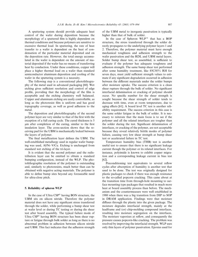
Fig. 15 is a cross-section photo of a typical bump
testing as open circuit during the test. It evidences that
the ultimate failure mode is the same normal solder wear-
out of the BON structure. The weakest point being the
solder wear-out means reliable, reproducible, and pre-
dictable results. The other failure modes like polymer
interfacial cracking are brittle resulting into relatively
low life time with lowWeibull slope. A possible reason to
observe higher Weibull life in Spheron is due to the dif-
ferent UBM sizes. Ultra CSP� had 280 lm diameter
UBM opening while Spheron had 300 lm UBM pad
diameter, a 23% increase in surface area. Based on the
previous test result [5], this increase in chip side UBM size
could increase the Weibull life by approximately 30%.
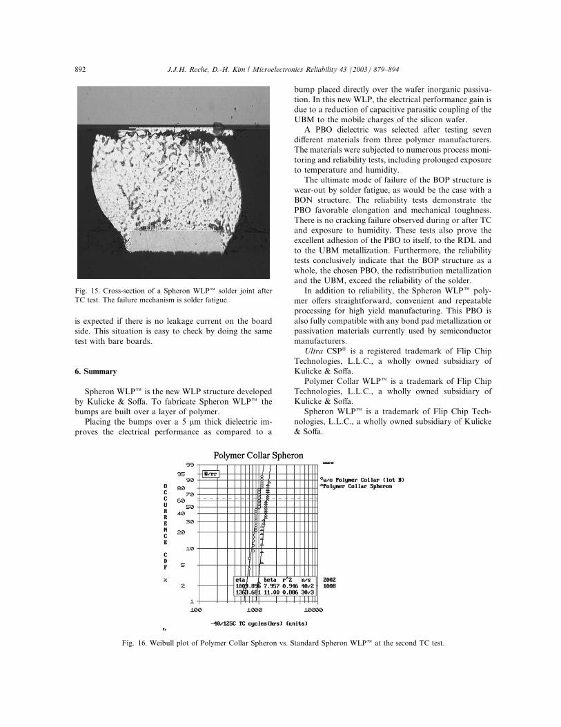
Polymer Collar WLPe is a polymer reinforcement
structureon the chip sideof the solder jointwhichhasbeen
the weakest point in TC tests in Ultra CSP� as well as in
Spheron, as shown in Fig. 15. It showed significant in-
Fig. 12. Weibull plot of Spheron WLPe (BOP) vs. Ultra CSP� (BON) at the first TC test.
Fig. 11. Representative of mixed shear fracture observed after
PCT. The top bump in the photograph exhibits a mixed mode
of the good and poor shear fractures.
890 J.J.H. Reche, D.-H. Kim / Microelectronics Reliability 43 (2003) 879–894

crease inWeibull life from thepreviousTC testswithUltra
CSP� [5]. Fig. 16 shows a Weibull plot of Spheron with
Polymer Collar in the second TC test. The figure indicates
that the Spheron structure with a Polymer Collar exhib-
its an approximate 35% improvement in Weibull life.
5.3. Wafer level bias test
Board level THB test is in progress. The CSP50 test
pattern was also used in this study. Two parallel 5 mm
long metal traces are placed on the RDL metal plane of
the chip. The traces are approximately 25 lm wide with40 lm space in-between.
Wafer level bias test was conducted. Using a probe
station, leakage current between the two metal traces
was measured after the lithography of the RDL metal
lines, again after the second polymer process, and once
more after solder bumping. The noise level with 5 V bias
on the two metal traces was about 1 nA with the probe
station and the leakage current was not detectable in any
cases. The wafers were then placed in an 85C/85% RH
chamber for seven days and the leakage current mea-
sured at completion. There was no detectable leakage
current. Based on the fact that all the wafer level bias
tests that did not show any detectable leakage current,
no abnormal leakage current at the board level THB test
Fig. 14. Weibull plot of Spheron WLPe (BOP) vs. Ultra CSP� (BON) at the second TC test.
Fig. 13. Weibull plot of three lots of Spheron WLPe at the second TC test.
J.J.H. Reche, D.-H. Kim / Microelectronics Reliability 43 (2003) 879–894 891
is expected if there is no leakage current on the board
side. This situation is easy to check by doing the same
test with bare boards.
6. Summary
Spheron WLPe is the new WLP structure developed
by Kulicke & Soffa. To fabricate Spheron WLPe the
bumps are built over a layer of polymer.
Placing the bumps over a 5 lm thick dielectric im-
proves the electrical performance as compared to a
bump placed directly over the wafer inorganic passiva-
tion. In this new WLP, the electrical performance gain is
due to a reduction of capacitive parasitic coupling of the
UBM to the mobile charges of the silicon wafer.
A PBO dielectric was selected after testing seven
different materials from three polymer manufacturers.
The materials were subjected to numerous process moni-
toring and reliability tests, including prolonged exposure
to temperature and humidity.
The ultimate mode of failure of the BOP structure is
wear-out by solder fatigue, as would be the case with a
BON structure. The reliability tests demonstrate the
PBO favorable elongation and mechanical toughness.
There is no cracking failure observed during or after TC
and exposure to humidity. These tests also prove the
excellent adhesion of the PBO to itself, to the RDL and
to the UBM metallization. Furthermore, the reliability
tests conclusively indicate that the BOP structure as a
whole, the chosen PBO, the redistribution metallization
and the UBM, exceed the reliability of the solder.
In addition to reliability, the Spheron WLPe poly-
mer offers straightforward, convenient and repeatable
processing for high yield manufacturing. This PBO is
also fully compatible with any bond pad metallization or
passivation materials currently used by semiconductor
manufacturers.
Ultra CSP� is a registered trademark of Flip Chip
Technologies, L.L.C., a wholly owned subsidiary of
Kulicke & Soffa.
Polymer Collar WLPe is a trademark of Flip Chip
Technologies, L.L.C., a wholly owned subsidiary of
Kulicke & Soffa.
Spheron WLPe is a trademark of Flip Chip Tech-
nologies, L.L.C., a wholly owned subsidiary of Kulicke
& Soffa.
Fig. 15. Cross-section of a Spheron WLPe solder joint after
TC test. The failure mechanism is solder fatigue.
Fig. 16. Weibull plot of Polymer Collar Spheron vs. Standard Spheron WLPe at the second TC test.
892 J.J.H. Reche, D.-H. Kim / Microelectronics Reliability 43 (2003) 879–894

Acknowledgements
The authors would like to thank Mr. Abhaya Khulbe
in Celestica for their board assembly support.
References
[1] Elenius P, Barrett S, Kim D-H. Wafer level packaging. In:
APACK 2001, An International Conference on Advances
in Packaging, Singapore, 5–7 December 2001.
[2] Elenius P. The Ultra CSP wafer level package. In: 4th Pan
Pacific Microelectronics Symposium, February 1999.
[3] Yang H, Elenius P, Barrett S, Schneider C, Leal J, Moraca
R, et al. Reliability characterization in ultra CSP package
development. In: IEEE 50th ECTC, Las Vegas, Nevada,
21–24 May 2000.
[4] Reche JJH. High density multichip interconnect and pack-
aging technology. In: IEEE IEMTWorkshop on Multichip
Interconnection, Orlando, FL, 10–13 October 1988.
[5] Kim D-H, Elenius P, Johnson M, Barrett S. Solder joint
reliability of a polymer reinforced wafer level package.
Microelectron Reliab 2002;42:1837;
Kim D-H, Elenius P, Johnson M, Barrett S. Solder joint
reliability of a polymer reinforced wafer level package. In:
IEEE 52nd ECTC 2002, San Diego, California, 28–31 May
2002;
Kim D-H, Elenius P, Barrett S. A polymer reinforced
WLP/why it has superior solder joint reliability. In:
IMAPS 2001, The 34th International Symposium on
Microelectronics, Baltimore, MA, 9–11 October 2001;
Kim D-H, Elenius P, Barrett S. Polymer Collar––a
polymer reinforced wafer level package solder bump. In:
IMAPS, HD International 2001, Santa Clara, CA, 18–20
April 2001;
Kim D-H, Elenius P, Barrett S. External polymer rein-
forcement of solder ball structure. In: IMAPS Advanced
Technology Workshop on CSP, North Falmouth, MA,
22–24 September 2000.
[6] Kim D-H, Elenius P, Barrett S. Solder joint reliability and
characteristics of deformation and crack growth of Sn–Ag–
Cu vs. eutectic Sn–Pb on a WLP in a thermal cycling test.
IEEE Trans Electron Pack Manuf 2002;25(2):84;
Kim D-H, Elenius P. Deformation and crack growth
characteristics of SnAgCu vs. 63Sn–Pb solder joints on a
WLP in thermal cycle testing. In: IEEE 51st ECTC,
Orlando, Florida, 28–31 May 2001.
[7] Deleonibus S. CMOS: how far can it go. Solid State
Technol 2000;43(3):S14.
[8] Reche J, Halahan P, Korczynsky R. Novel high-volume
manufacturing technology for 3-D IC packages. In: The
Fifth VLSI Packaging Workshop of Japan, Kyoto, Japan,
4–6 December 2000.
[9] Spielberger RK, Huang CD, Nunne WH, Mones AH, Fett
DL, Hampton FL. Silicon on silicon packaging. IEEE
Trans Compon Hybrids Manuf Technol 1984;7:193.
[10] Bartlett CJ. Multichip packaging for VLSI. Solid State
Technol 1986;(June):119.
[11] Neue Trends in der Geh€aausetechnik. Mikro Electronik
1990;4:216.
[12] Kimijima S, Miyagi T, Sudo T. High-density multichip
module by chip-on-wafer technology. In: Proceedings of
ISHM International, vol. 314, 1988.
[13] Treece RK. Technology overview. In: mBGA Commer-
cialization Project Workshop, April 1994.
[14] Deutsch A et al. High-speed signal propagation on lossy
transmission lines. IBM J Res Develop 1990;34(4):601.
[15] Rubin BJ. Electrical characterization of the interconnects
inside a computer. In: International Conference on Ad-
vances in Interconnections and Packaging, SPIE vol. 1389,
1990.
[16] Edward Lee M-J, Dally WJ (Member IEEE), Chiang P.
Low-power area-efficient high-speed I/O circuit techniques.
IEEE J Solid-State Circ 2000;35(11):1591.
[17] Chang WH. Analytical IC metal-line capacitive formulas.
IEEE Trans Microwave Theory Tech 1976;MTT-24:603.
[18] Williams DF, Hayden LA, Marks RB. A complete
multimode equivalent-circuit theory for electrical design.
J Res Natl Inst Stand Technol 1997;102:405.
[19] Heinrich W, Jentzsch A, Baumann G. Millimeter-wave
characteristics of flip-chip interconnect for multichip
modules. IEEE Trans Microwave Theory Tech 1998;46:
2264.
[20] Marks RB, Jargon JA, Pao CK, Wen CP. Electrical mea-
surements of microwave flip-chip interconnections. In: Int-
ernational Symposium on Microelectronics, ISHM, 1995.
[21] Bogert TM, Renshaw RR. J Am Chem Soc 1908;30:1137.
[22] Edwards WM, Robertson IM. US Patent No. 2,710853,
1955.
[23] Epifano RN, Jordan EL. Method of making a semicon-
ductor device including a polyimide resist film, filed April
8, 1970, issued October 24, 1972.
[24] Harada S, Nanogaki S, Okabe T, Kohashi T, Sato K.
Multilayer interconnected structure for semiconductor
integrated circuit and process for manufacturing the same.
US Patent No. 3,801,880, applied for September 11, 1972,
issued April 2, 1974.
[25] Ryan JG, Geffken RM, Poulin NR, Paraszczak JR. The
evolution of interconnection technology at IBM. J Res Dev
1995;39(4):371.
[26] Kerwin RE, Goldrick MR. Thermally stable photoresist.
In: Second Technical Conference on Photo-polymers, 15
October 1970.
[27] Clerc LP. La Technique Photographique. 2nd ed. Paris:
Paul Montel Publisher; 1934.
[28] Reche JJH. Fast-turnaround indirect–direct dichromated
thick film screens. In: ISHM Northwest Chapter Meeting,
10 December 1976.
[29] Rubner R. Production of highly heat-resistant film pat-
terns from photoreactive polymeric precursor. Part 1 and
2. Siemens Forsch -u Entwickl -Ber 1976;5:235.
[30] Reche JJH. Material selection for VLSI multichip modules.
In: Third Electronic Materials & Processes Conference,
SAMPE, Los Angeles, CA, vol. 3, 20–22 June 1989. p. 948.
[31] Frazer AH. High temperature resistant polymers. New
York, NY: John Wiley & Sons; 1968.
[32] Scola DA. High temperature polyimides. Chemtech
1989;19:112.
[33] St Clair AK, St Clair TL. Structures from low dielectric
polyimides. US Patent No. 5,338,826, issued August 16,
1994.
J.J.H. Reche, D.-H. Kim / Microelectronics Reliability 43 (2003) 879–894 893

[34] Barie Jr. W, Walter P. Preparation of acetylene-substituted
polyimide oligomers and polyimide polymers. US Patent
No. 4,097,456, issued June 27, 1978.
[35] Rabilloud G, Sillion B, De Gaudemaris G. Mixed imide-
isoindoloquinazolinediones heterocyclic polymers. US Pa-
tent No. 3,678,005, applied for April 14, 1970, issued July
18, 1972.
[36] Williams III FJ. Polythioetherimides and method of
preparation. US Patent No. 3,933,749, January 20, 1976.
[37] Verdet L, Reche J. The P�s and Q�s of PPQ. ElectronPackag Prod 1991;31(January):58.
[38] Labadie JW, Hedrick JL. Recent advances in high
temperature polymers for microelectronics applications.
SAMPE J 1989;25(6):18.
[39] Elce E, Hay AS. A new synthesis of bisbenzils and novel
poly(phenylquinoxaline)s therefrom. Polymer 1996;37:
1745.
[40] Labelle CB, Gleason KK. Overhang test structure depo-
sition profiles of pulsed plasma fluorocarbon films form
hexafluoropropylene oxide, 1,1,2,2-tetrafluoroethane and
difluoromethane. Adv Mater Chem Dep 2000;6:27.
[41] Hanford WE, Roland JE. Tetrafluoroethylene copolymers.
US Patent No. 4,530,569, issued April 26, 1949.
[42] Stille JK. Quinoxaline polymers, methods of making same
and compositions thereof. US Patent No. 3,661,850, issued
May 9, 1972.
[43] Brinker KC, Robinson IM. Polybenzimidazoles. US Patent
No. 2,895,948, issued July 29, 1959.
[44] Brinker KC, Cameron DD, Robinson IM. Polybenzox-
azoles. US Patent No. 2,904,537, issued September 15,
1959.
[45] Ahne H, Hammerschmidt A. Heat resistant positive resists
and method for preparing heat-resistant relief structures.
US Patent No. 4,849,051, issued July 18, 1989.
[46] Vergne J, Solaux L, Robinet JC, Lacroix P. Compositions
of polymer of bicycla (2-2-1) heptene-2 and derivatives. US
Patent No. 3,676,390, issued July 11, 1972.
[47] Kovar RF, Arnold FE. Addition curable phenyl-quinox-
aline compositions and their synthesis. US Patent No.
3,966,729, issued June 29, 1976.
[48] Tani Y, Endou M, Ogawa K, Tanaka Y, Yasuhisa I,
Ishihara T, Kubota T. Light-sensitive polymer, method for
preparing the same and method for forming patterns. US
Patent No. 5,254,439, issued October 19, 1993.
[49] Gorham WF. Halogeneted di-p-xylylenes. US Patent No.3,221,068, issued November 30, 1965.
[50] Finkelstein H. Doctoral dissertation on 1,2 dibromobenzo-
cyclobutene. Student of Johannes Thiele, University of
Strassburg, 1909.
[51] Finkelstein H. Darstellung Organisher Jodide aus den
Enterprechenden Brominen und Chloriden. Chem Ber
(Berichte der Deutschen Chemischen Gesellschaft) 1910;
43:1528.
[52] Sezi R, Ahne H, Kuehn E, Eberhard K, Gestigkeit R.
Preparation of poly-O-hydroxyamides and poly-O-mer-
captoamides. US Patent No. 5,807,969, issued September
15, 1998.
[53] LaRochelle RW. Process for making silarylenesilane-
diol, silarylenesiloxanediol and silarylenesiloxane-poly-
diorganosiloxane block copolymers. US Patent No.
3,959,403, issued May 25, 1976.
[54] Marvel CS, Vogel HA. Polybenzimidazoles and their
preparation. US Patent No. 3,174,947, issued March 23,
1965.
[55] Grassie N, Scott G. Polymer degradation and stabilisation.
Cambridge, UK: Cambridge University Press; 1985.
[56] Reche JJH. Thin film multichip modules, a primer source
book. Karl S€uuss America; 1993. Publication # 119.
[57] Reche JJH. Polyimides in hybrid circuit processing.
Semicond Int 1986;9(9):116.
[58] Aronhime MT, Gillham JK. The transformation of liquid
to amorphous solid: effect of reaction mechanism on the
time to vitrify for linear and network polymerization. J
Coating Technol 1984;56:35.
[59] Reche JJH. Control of thin film materials properties used
in high density multichip interconnect. In: Material
Research Society Symposium K, Electronic Packaging
Material Science, San Diego, CA, vol. 154, 24–28 April
1989. p. 39.
[60] Reche JJH. Fabrication of high density multichip modules.
In: Proc. 7th IEEE/CHMT International Electronic Man-
ufacturing Technical Symposium, San Francisco, CA, 25–
27 September 1989. p. 104.
[61] Coyle RJ, Solan PP, Serafino AJ, Gahr SA. The influence
of room temperature aging on ball shear strength and
microstructure of area array solder balls. In: IEEE 50th
ECTC, Las Vegas, Nevada, 21–24 May 2000.
[62] Watamabe M. J Electron Commun 1988;J71-C(11):1510.
894 J.J.H. Reche, D.-H. Kim / Microelectronics Reliability 43 (2003) 879–894