wolfspeed ptma180402m v1 product and characteristics spec … · gate-source voltage vgs –0.5 to...
TRANSCRIPT

All published data at TCASE = 25°C unless otherwise indicated
ESD: Electrostatic discharge sensitive device—observe handling precautions!
4600 Silicon Drive | Durham, NC 27703 | www.wolfspeed.comRev. 10, 2018-05-19
RF Characteristics
CDMA Measurements (tested in Wolfspeed production test fixture)VDD = 28 V, IDQ1 = 160 mA, IDQ2 = 360 mA, POUT = 4 W average, ƒ = 1960 MHz, CDMA IS-95, 9 channels
Characteristic Symbol Min Typ Max Unit
Gain Gps 28 30 — dB
Drain Efficiency hD 14 16 — %
Adjacent Channel Power Ratio ACPR — –52 –50 dBc
RF Characteristics continued next page
Wideband RF LDMOS Integrated Power Amplifier40 W, 28 V, 1800 – 2100 MHz
Description
The PTMA180402M is a matched, wideband, 2-stage, 40-watt LDMOS integrated amplifier intended for base station applications in the 1800 to 2100 MHz frequency band. This device is offered in a 20-pin, thermally-enhanced, overmolded plastic package for cool and reliable operation.
PTMA180402M Package PG-DSO-20-63
Features
• Designed for wide RF bandwidth and low memory effects
• On-chip matching, integrated input DC block, 50-ohm input and ~4-ohm output
• Typical single-carrier CDMA performance at 1960 MHz, 28 V - Average output power = 5 W - Linear gain = 30 dB - Efficiency = 16% - Adjacent channel power = –52 dBc
• Typical two-tone CW performance at 1960 MHz, 28 V - Output power (PEP) = 40 W at IMD3 = –30 dBc - Efficiency = 34%
• Capable of handling 10:1 VSWR @ 28 V, 40 W (CW) output power
• Integrated ESD protection. Meets HBM Class 1B (minimum), per JESD22-A114F
• Thermally-enhanced, RoHS-compliant package
-25
-20
-15
-10
-5
0
5
10
14
18
22
26
30
34
1700 1800 1900 2000 2100 2200
Ret
urn
Loss
(dB
)
Gai
n(d
B)
Frequency (MHz)
Broadband PerformanceVDD = 28 V, IDQ1 = 160 mA, IDQ2 = 360 mA,
Fixture tuned for 1930 - 1990 MHz
Gain
Return Loss
PTMA180402M

4600 Silicon Drive | Durham, NC 27703 | www.wolfspeed.comRev. 10, 2018-05-19
2PTMA180402M
RF Characteristics (cont.)
Two-tone Specifications (not subject to production test—verified by design/characterization in Wolfspeed test fixture)VDD = 28 V, IDQ1 = 160 mA, IDQ2 = 360 mA, POUT = 40 W PEP, ƒ = 1960 MHz, tone spacing = 1 MHz
Characteristic Symbol Min Typ Max Unit
Gain Gps — 30 — dB
Power Added Efficiency PAE — 34 — %
Third Order Intermodulation Distortion IMD3 — –32 — dBc
DC Characteristics
Stage 1 Characteristics Conditions Symbol Min Typ Max Unit
Drain Leakage Current VDS = 28 V, VGS = 0 V IDSS — — 1.0 µA
VDS = 63 V, VGS = 0 V IDSS — — 10.0 µA
Gate Leakage Current VGS = 10 V, VDS = 0 V IGSS — — 1.0 µA
On-state Resistance Stage 1 VGS = 10 V, VDS = 0.1 V RDS(on) — 1.6 — Ω
Operating Gate Voltage VDS = 28 V, IDQ1 = 160 mA, VGS 2.0 2.5 3.0 V
Stage 2 Characteristics Conditions Symbol Min Typ Max Unit
Drain-source Breakdown Voltage VGS = 0 V, IDS = 10 mA V(BR)DSS 65 — — V
Drain Leakage Current VDS = 28 V, VGS = 0 V IDSS — — 1.0 µA
VDS = 63 V, VGS = 0 V IDSS — — 10.0 µA
Gate Leakage Current VGS = 10 V, VDS = 0 V IGSS — — 1.0 µA
On-state Resistance Stage 2 VGS = 10 V, VDS = 0.1 V RDS(on) — 0.21 — Ω
Operating Gate Voltage VDS = 28 V, IDQ2 = 360 mA VGS 2.0 2.5 3.0 V

4600 Silicon Drive | Durham, NC 27703 | www.wolfspeed.comRev. 10, 2018-05-19
3PTMA180402M
Maximum Ratings
Parameter Symbol Value Unit
Drain-Source Voltage VDSS 65 V
Gate-Source Voltage VGS –0.5 to +12 V
Junction Temperature TJ 200 °C
Total Device Dissipation PD 175 W
Above 25°C derate by 1.0 W/°C
Storage Temperature Range TSTG –40 to +150 °C
Overall Thermal Resistance Stage 1, IDQ1 = 160 mA RqJC 3.6 °C/W(TCASE = 70°C, 40 W CW)
Stage 2, IDQ2 = 360 mA RqJC 1.5 °C/W
Moisture Sensitivity Level
Level Test Standard Package Temperature Unit
3 IPC/JEDEC J-STD-020 260 °C
Ordering Information
Type and Version Order Code Package and Description Shipping
PTMA180402M V1 R500 PTMA180402M-V1-R500 PG-DSO-20-63, molded plastic Tape & Reel, 500 pcs

4600 Silicon Drive | Durham, NC 27703 | www.wolfspeed.comRev. 10, 2018-05-19
4PTMA180402M
Typical Performance, circuit tuned for 2140 MHz (data taken in Wolfspeed test fixture)
25
35
45
55
-50
-40
-30
-20
ded
Effic
ienc
y (%
)
MD
3 (d
Bc)
Two-tone Drive UpVDD = 28 V, IDQ1 = 150 mA, IDQ2 = 400 mA,
ƒ = 2140 MHz, 1 MHz tone spacing
IM3L
5
15
25
-70
-60
50
29 31 33 35 37 39 41 43 45
Pow
er A
ddIM
Average Output Power (dBm)
IM3UPower Added Efficiency
-32
-22
-12
-2
8
18
28
10
14
18
22
26
30
34
1700 1900 2100 2300 2500
Inpu
tRet
urn
Loss
( dB
)
Gai
n(d
B)
Frequency (MHz)
Broadband SweepVDD = 28 V, IDQ1 = 150 mA, IDQ2 = 400 mA,
Fixture tuned for 2110 - 2170 MHz
Gain
IRL
5
15
25
35
45
55
65
10
14
18
22
26
30
34
30 32 34 36 38 40 42 44 46
Gai
n(d
B)
Output Power (dBm)
Power Sweep, P-1dBVDD = 28 V, IDQ1 = 150 mA, IDQ2 = 400 mA
2110 MHz2140 MHz2170 MHz
Gain
Pow
erA
dded
Eff
icie
ncy
(%)
Power AddedEfficiency
25
35
45
55
-50
-40
-30
-20
ed E
ffici
ency
(%)
MD
3 (d
Bc
Two-tone Drive UpVDD = 28 V, IDQ1 = 150 mA, IDQ2 = 400 mA,
1 MHz tone spacing
2110 MHz2140 MHz2170 MHz
5
15
25
-70
-60
-50
29 31 33 35 37 39 41 43 45
Pow
er A
ddI M
Average Output Power (dBm)
Power Added Efficiency
IMD
3 (d
Bc)
IMD3
4600 Silicon Drive | Durham, NC 27703 | www.wolfspeed.comRev. 10, 2018-05-19
5PTMA180402M
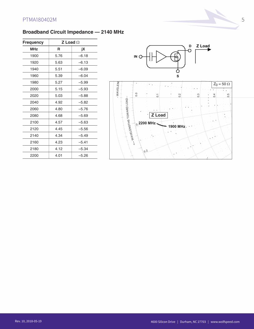
Broadband Circuit Impedance — 2140 MHz
Frequency Z Load Ω
MHz R jX
1900 5.76 –6.18
1920 5.63 –6.13
1940 5.51 –6.09
1960 5.39 –6.04
1980 5.27 –5.99
2000 5.15 –5.93
2020 5.03 –5.88
2040 4.92 –5.82
2060 4.80 –5.76
2080 4.68 –5.69
2100 4.57 –5.63
2120 4.45 –5.56
2140 4.34 –5.49
2160 4.23 –5.41
2180 4.12 –5.34
2200 4.01 –5.26
Z LoadD
S
IN
0.1
0.3
0.5
0.2
0.4
0.1
0.3
0.5
0.7
0.9
0.2
0.4
0.6
0.8
0.1
0.3
0.5
0.7
0.9
0.2
0.4
0.6
0.8
1
-WA
VE
LEN
GTH
STO
WA
RDG
ENER
ATO
R---
>
0.05
0.40
0.45
0.05
0.10
0.45
<---
WA
VELE
NG
THS
TOW
AR
DLO
AD
- 0.0
Nornalized to 50 Ohms
a180402m-2140 MHz
2200 MHz1900 MHz
da180402m2140 Sept. 20, 2009 8:20:58 PM
Z Load
Z0 = 50 Ω

4600 Silicon Drive | Durham, NC 27703 | www.wolfspeed.comRev. 10, 2018-05-19
6PTMA180402M
Reference Circuit, tuned for 2140 MHz
Reference circuit schematic for ƒ = 2140 MHz
Circuit Description DUT PTMA180402M, LDMOS IC
PCB Rogers RO4350, 0.76 mm [.030"] thick, er = 3.48, 1 oz. copper Test fixture part no. LTN/PTMA180402M-21Find Gerber files for this test fixture on the Wolfspeed Web site at (www.wolfspeed.com/RF)
Circuit Assembly Information
Microstrip Electrical Characteristics Dimensions: L x W (mm) Dimensions: L x W (in.)
at 2140 MHzl1 0.150 λ, 50.0 Ω 12.73 x 1.70 0.501 x 0.067
l2 0.177 λ, 50.0 Ω 15.04 x 1.70 0.592 x 0.067
l3 0.026 λ, 10.4 Ω 2.01 x 13.00 0.079 x 0.512
l4 0.026 λ, 10.4 Ω 2.06 x 13.00 0.081 x 0.512
l5 0.026 λ, 34.2 Ω 2.13 x 3.00 0.084 x 0.118
l6 0.054 λ, 34.2 Ω 4.45 x 3.00 0.175 x 0.118
l7 0.066 λ, 43.5 Ω 5.56 x 2.11 0.219 x 0.083
l8 0.178 λ, 43.5 Ω 14.96 x 2.11 0.589 x 0.083
l9 0.059 λ, 50.0 Ω 5.03 x 1.70 0.198 x 0.067
l10, l11 0.137 λ, 47.8 Ω 11.56 x 1.83 0.455 x 0.072
C1100µF 50V
R20O
C1110µF
Q2
G1
G2V
R4
R10O
R3
V
C710µF
Q1
VD1
C1810µF
C160.1µF
C1512pF
C171µF
C130.1µF
C121µF
C1412pF
C512pF
1
C90.1µF
C81µF
C1012pF
J1
C31µF
C210µF
C40.1µF
183
PTMA180402M
10
89
7
4
65
11121314151617
21
DUT
1920
9
C29100µF 50V
C271µF
C2512pF
C260.1µF
C2810µF
C19100µF 50V
C2012pF
C301.8pF
4
C311.8pF
D1V
3
11
5
10
C322.4pF
6 7
C331.2pF
8
C3412pF
C210.1µF
C221µF
C2310µF
J2
VD2
C24100µF 50V
2
C6.5pF
M A 1 8 0 4 0 2 m _ 2 1 4 0 M H z _ B D _ 9 - 2 - 0 9
RF_IN RF_OUT

4600 Silicon Drive | Durham, NC 27703 | www.wolfspeed.comRev. 10, 2018-05-19
7PTMA180402M
Reference Circuit — 2140 MHz (cont.)
Assembly diagram for 2140 MHz reference circuit (not to scale)
Component Description Manufacturer P/N or CommentC1, C19, C24, C29 Electrolytic capacitor, 100 µF, 50 V Panasonic Electronic Components EEV-FK1H101GPC2, C7, C11, C18, Ceramic capacitor, 10 µF Murata GRM422Y5V106Z050AL C23, C28C3, C8, C12, C17, Ceramic capacitor, 1 µF TDK Corporation C4532X7R2A105M230KA C22, C27C4, C9, C13, C16, Capacitor, 0.1 µF Kemet C1210C104K5RACTU C21, C26 C5, C10, C12, C15, Ceramic capacitor, 12 pF ATC 600S120JT C20, C25, C34C6 Ceramic capacitor, 0.5 pF ATC 100B 0R5C30, C31 Ceramic capacitor, 1.8 pF ATC 600S1R8CTC32 Ceramic capacitor, 2.4 pF ATC 100B 2R4C33 Ceramic capacitor, 1.2 pF ATC 100B 1R2Q1, Q2 Transistor Infineon Technologies BCP56R1, R2 Resistor, 0 Ω Panasonic Electronic Components ERJ-3GEY0R00VR3, R4 Potentiometer, 2k Ω Bourns, Inc. 3224W-1-202E
C6
C33
R1
R2
C24C23C22
C21
C20
C29
C28C27
C26
C25
C32 C34C31
C30
C1C2
C3
C4C5
C19
C15
C16C17C18
C7
C8C9 C13
C14C10
C11C12
M A 1 8 0 4 0 2 m _ 2 1 4 0 M H z _ C D _ 9 - 2 - 0 9
VG2
VD1
VG
1
VD2
VD2VD1
RF_IN RF_OUT
R3R4
Q2Q1
PTMA180402M_02A

4600 Silicon Drive | Durham, NC 27703 | www.wolfspeed.comRev. 10, 2018-05-19
8PTMA180402M
Typical Performance, circuit tuned for 1960 MHz (data taken in a production test fixture)
0
10
20
30
40
50
60
26
27
28
29
30
31
32
30 32 34 36 38 40 42 44 46 48
Gai
n(d
B)
Output Power (dBm)
CW Power PerformanceVDD = 28 V, IDQ1 = 130 mA, IDQ2 = 360 mA,
ƒ = 1930, 1960, 1990 MHz
1930 MHz
1960 MHz
1990 MHz
Gain
Pow
erA
dded
Eff
ici e
ncy
(%)
Efficiency
26
27
28
29
30
31
32
30 32 34 36 38 40 42 44 46
Gai
n(d
B)
Output Power (dBm)
CW Performance atSelected Drain Voltage
VDD = 24 V, 28 V, 32 VIDQ1 = 130 mA, IDQ2 = 360 mA, ƒ = 1960 MHz
24 V
32 V
28 V
-60
-50
-40
-30
-20
-10
0
10
20
30
40
50
30 32 34 36 38 40 42 44 46
IMD
3(d
Bc)
Average Output Power ( dBm )
Two-tone Drive-upVDD = 28 V, IDQ1 = 160 mA, IDQ2 = 360 mA
ƒ = 1930, 1960, 1990 MHz
1930 MHz
1960 MHz
1990 MHzEfficiency
IMD3Pow
erA
dded
Eff
icie
ncy
(%)
0
5
10
15
20
25
30
-65
-60
-55
-50
-45
-40
-35
29 31 33 35 37 39 41
Pow
erA
dded
Eff
icie
ncy
(%)
Output Power (dBm)
CDMA IS-95 Drive-up, 3 FrequenciesVDD = 28 V, IDQ1 = 160, IDQ2 = 360 mA,
ƒ = 1930, 1960, 1990 MHz
1930 MHz
1960 MHz
1990 MHz
Adj
acen
tCha
nnel
Pow
erR
atio
(dB
)
Efficiency
ACPR
Power AddedEfficiency
Power AddedEfficiencyPower Added
Efficiency

4600 Silicon Drive | Durham, NC 27703 | www.wolfspeed.comRev. 10, 2018-05-19
9PTMA180402M
Typical Performance —1960 MHz (cont.)
Edge Modulation PerformanceVDD = 28 V, IDQ1 = 160 mA, IDQ2 = 360 mA
ƒ = 1930 1960 1990 MHz
-5040
ƒ = 1930, 1960, 1990 MHz
c)
-60
-55
30
35
400 kHz
1930 MHz1960 MHz1990 MHz
ctru
m (d
B
ency
(%)
-70
-65
20
25
atio
n Sp
ec
ded
Effic
ie
-80
-75
10
15
600 kHz ge M
odul
a
Pow
er A
dd
Power Added Efficiency
-85
80
5
10
30 32 34 36 38 40 42 44
EdgP
Output Power ( dBm )
-40
-35
-30
-25
-20
15
20
25
30
35
M3
(dBc
)
Two-carrier WCDMA Drive-up VDD = 28 V, IDQ1 = 160 mA, IDQ2 = 360 mA,
ƒ = 1930, 1960, 1990 MHz, PAR = 8 dB, 10 MHz spacing, 3.84 MHz bandwidth
1930 MHz1960 MHz1990 MHz
dded
Effi
cien
cy (%
) Power Added Efficiency
-50
-45
40
5
10
15
30 32 34 36 38 40 42
I
Output Power ( dBm )
IM3Pow
er A
d
Edge EVM PerformanceVDD = 28 V, IDQ1 = 160 mA, IDQ2 = 360 mA
ƒ = 1930 1960 1990 MHz
3.540
ƒ 1930, 1960, 1990 MHz
2.5
3.0
30
35
de (%
)
ncy
(%)
1930 MHz1960 MHz1990 MHz
1.5
2.0
20
25
r Mag
nitu
d
ed E
ffici
en
Power Added
0 5
1.0
10
15
ror V
ecto
rEVM
ower
Add
e Efficiency
0.0
0.5
5
10
30 32 34 36 38 40 42 44
Err
Po
Output Power ( dBm )
-35
-30
-25
-20
20
25
30
35
M3
(dBc
)
Two-carrier WCDMA at Selected Temperatures
VDD = 28 V, IDQ1 = 160 mA, IDQ2 = 360 mA, ƒ = 1960 MHz, PAR = 8 dB, 10 MHz spacing,
3.84 MHz bandwidth
25°C90°C
–25°C Power Added Efficiency
dded
Effi
cien
cy (%
)
-50
-45
-40
5
10
15
30 32 34 36 38 40 42
IM
Output Power ( dBm )
IM3Pow
er A
d

4600 Silicon Drive | Durham, NC 27703 | www.wolfspeed.comRev. 10, 2018-05-19
10PTMA180402M
Broadband Circuit Impedance — 1960 MHz
Z LoadD
S
IN
Frequency Z Load Ω
MHz R jX
1800 5.56 –6.95
1810 5.48 –6.91
1820 5.39 –6.87
1830 5.31 –6.83
1840 5.23 –6.79
1850 5.15 –6.75
1860 5.07 –6.70
1870 4.99 –6.66
1880 4.91 –6.61
1890 4.84 –6.56
1900 4.76 –6.51
1910 4.69 –6.47
1920 4.61 –6.42
1930 4.54 –6.36
1940 4.47 –6.31
1950 4.40 –6.26
1960 4.33 –6.21
1970 4.26 –6.15
1980 4.19 –6.10
1990 4.12 –6.04
2000 4.06 –5.99
0.1
0.3
0.5
0.2
0.4
0.1
0.3
0.5
0.7
0.9
0.2
0.4
0.6
0.8
0.1
0.30.
5
0.7
0.9
0.2
0.40.
6
0.8
1
-WA
VE
LEN
GTH
STO
WA
RDG
ENER
ATO
R---
>
0.05
0.40
0.45
0.05
0.10
0.45
<---
WA
VELE
NG
THS
TOW
AR
DLO
AD
- 0.0
Nornalized to 50 Ohms
a180402m-1900 MHz
2200 MHz 1800 MHz
da180402m1900 Sept. 20, 2009 8:34:45 PM
Z Load
Z0 = 50 Ω

4600 Silicon Drive | Durham, NC 27703 | www.wolfspeed.comRev. 10, 2018-05-19
11PTMA180402M
Reference Circuit, tuned for 1960 MHz
Reference circuit schematic for ƒ = 1960 MHz
Circuit Description
DUT PTMA180402M, LDMOS IC
PCB Rogers RO4350, 0.76 mm [.030"] thick, er = 3.48, 1 oz. copper Test Fixture Part No. LTN/PTMA180402MFind Gerber files for this test fixture on the Wolfspeed Web site at (www.wolfspeed.com/RF)
Microstrip Electrical Characteristics Dimensions: L x W (mm) Dimensions: L x W (in.)
at 1960 MHzl1 0.300 λ,50.0 Ω 27.76 x 1.70 1.093 x 0.067
l2 0.024 λ,10.4 Ω 2.01 x 13.00 0.079 x 0.512
l3 0.024 λ,10.4 Ω 2.06 x 13.00 0.081 x 0.512
l4 0.037 λ,34.2 Ω 3.35 x 3.00 0.132 x 0.118
l5 0.046 λ,34.2 Ω 4.11 x 3.00 0.162 x 0.118
l6 0.097 λ,34.2 Ω 8.76 x 3.00 0.345 x 0.118
l7 0.127 λ,43.6 Ω 11.63 x 2.11 0.458 x 0.083
l8 0.054 λ,50.0 Ω 5.03 x 1.70 0.198 x 0.067
l9, l10 0.125 λ,47.8 Ω 11.56 x 1.83 0.455 x 0.072
C71µF
C912pF
C80.1µF
C610µF
C1312pF
G2V
C111µF
C1010µF
C120.1µF
C161µF
C1412pF
C150.1µF
C18100µF 50V
C1710µF
D1V
VD1
G1V
J1
C1100µF 50V
C210µF
C31µF
DUT
PTMA180402M
3
1
7
910
8
56
4
C40.1µF
C512pF
12
C291.8pF
18
14131211
171615
C301.8pF
2 3
2019
C2710µF
C250.1µF
C2412pF
10
C261µF
C28100µF 50V
VD2
C3312pF
5
C312.7pF
4 7
9
C1912pF
C200.1µF
C211µF
8 J2
C23100µF 50V
C2210µF
R10O
R20O
R4
R3
Q2
Q1
6
C321pF
M A 1 8 0 4 0 2 m _ 1 9 6 0 M H z _ B D _ 9 - 2 - 0 9
RF_IN RF_OUT

4600 Silicon Drive | Durham, NC 27703 | www.wolfspeed.comRev. 10, 2018-05-19
12PTMA180402M
Reference Circuit — 1960 MHz (cont.)
Assembly diagram for 1960 MHz reference circuit (not to scale)
Component Description Manufacturer P/N or CommentC1, C18, C23, C28 Electrolytic capacitor, 100 µF, 50 V Panasonic Electronic Components EEV-FK1H101GP
C2, C6, C10, C17, Ceramic capacitor, 10 µF Murata GRM422Y5V106Z050AL C22, C27C3, C7, C11, C16, Ceramic capacitor, 1 µF TDK Corporation C4532X7R2A105M230KA C21, C26C4, C8, C12, C15, Capacitor, 0.1 µF Kemet C1210C104K5RACTU C20, C25 C5, C9, C13, C14, Ceramic capacitor, 12 pF ATC 600S120JT C19, C24, C33C29, C30, C31 Ceramic capacitor, 1.8 pF ATC 600S1R8CTC32 Ceramic capacitor, 1.0 pF ATC 100B 1R0Q1, Q2 Transistor Infineon Technologies BCP56R1, R2 Resistor, 0 Ω Panasonic Electronic Components ERJ-3GEY0R00VR3, R4 Potentiometer, 2k Ω Bourns, Inc. 3224W-1-202E
C32
C23C22C21
C20
C19
C28
C27C26
C25
C24
C31 C33C30
C29
C1C2
C3C4
C5
C18
C14
C15C16
C17
C6
C7C8 C12
C13C9
C10C11
R1
M A 1 8 0 4 0 2 m _ 1 9 6 0 M H z _ C D _ 9 - 2 - 0 9
R4R2
Q2Q1
R3VG1
VG2
VD2
VD1
VD1 VD2
RF_IN RF_OUT
PTMA180402M_02A

4600 Silicon Drive | Durham, NC 27703 | www.wolfspeed.comRev. 10, 2018-05-19
13PTMA180402M
Pinout Diagram
1
2
3
4
5
6
7
8
9
10
20
19
18
17
16
15
14
13
12
11
Thermal FET
a 1 8 0 4 0 2 m _ p d _ 9 - 3 - 2 0 0 9
VD2, RF Out
VD2, RF Out
VD2, RF Out
VD2, RF Out
VD2, RF Out
VD2, RF Out
NC
NC
NC
NC
RF In
RF In
VG Thermal FET
VD Thermal FET
VD1
VD1
VD1
VD1
VG1
VG2
Source: plated copper heat slug on backside of package

4600 Silicon Drive | Durham, NC 27703 | www.wolfspeed.comRev. 10, 2018-05-19
14PTMA180402M
Package Outline Specifications
Package PG-DSO-20-63
Diagram Notes—unless otherwise specified:1. Interpret dimensions and tolerances per ASME Y14.5M-1994.
2. Package dimensions: 11.0 mm by 15.9 mm by 3.35 mm.
3. JEDEC drawing number: MO-166.
4. Does not include plastic or metal protrusion of 0.15 mm max per side.
5. Does not include dambar protrusion; maximum allowable dambar protrusion shall be 0.08 mm.
6. Bottom metallization. Sn plating (matte): 5 – 15 micron [196.85 – 590.55 microinch].
2X 2.90 [0.114] MAX
(2 PLS)
13.00 [0.512] MAX
110
11 20
6.
INDEX PIN 1
6.
14.20±0.30
11.00 [0.433]
9 X 1.27 = 11.439 X .050 = .450 1.10
[0.043] MAX (2 PLS)
2.95 [0.116]
6.00 [0.236]
TOP VIEW
BOTTOM VIEW
[0.559±0.012]
0.40+0.13[0.015+0.005]
0.25mm C A B
15.90±0.10 [0.626±0.004]
1.27 [0.050]
14°±1° (2 PLS)TOP/BOTTOM
ALL SIDES
11.00±0.10 [0.433±0.004]
5.
3.50 [0.137] MAX
SEE DETAIL A4.
SIDE VIEW
END VIEW
M S S
0.95±0.15 [0.037±0.006]
0.35 [0.014]GAUGE PLANE
0.15 [0.006] REF
0+0.1[0+0.004]
STANDOFF 1.60 [0.063] REF
0.25+0.07–0.02
[0.010 ]+0.003–0.001
DETAIL A
PG-DSO-20-63_ po_01_12-07-2012
Diagram Notes–unless otherwise specified:
1. Interpret dimensions and tolerances per ASME Y14.5M-1994.
2. Package dimensions: 11.0 mm by 15.9 mm by 3.35 mm.
3. JEDEC drawing number : MO-166.
4. Does not include plastic or metal protrusion of 0.15 mm max per side.
5. Does not include dambar protrusion; maximum allowable dambar protrusion shall be 0.08 mm.
6. Bottom metallization.
7. Sn plating (matte) : 5 - 15 micron [196.85 – 590.55 microinch].

www.wolfspeed.comRev. 10, 2018-05-19
Notes
Disclaimer
Specifications are subject to change without notice. Cree, Inc. believes the information contained within this data sheet to be accurate and reliable. However, no responsibility is assumed by Cree for any infringement of patents or other rights of third parties which may result from its use. No license is granted by implication or otherwise under any patent or pat-ent rights of Cree. Cree makes no warranty, representation or guarantee regarding the suitability of its products for any particular purpose. “Typical” parameters are the average values expected by Cree in large quantities and are provided for information purposes only. These values can and do vary in different applications and actual performance can vary over time. All operating parameters should be validated by customer’s technical experts for each application. Cree products are not designed, intended or authorized for use as components in applications intended for surgical implant into the body or to support or sustain life, in applications in which the failure of the Cree product could result in personal injury or death or in applications for planning, construction, maintenance or direct operation of a nuclear facility.
Copyright © 2018 Cree, Inc. All rights reserved. The information in this document is subject to change without notice. Wolfspeed™ and the Wolfspeed logo are trademarks of Cree, Inc.
For more information, please contact:
4600 Silicon DriveDurham, North Carolina, USA 27703www.wolfspeed.com/RF
Sales Contact [email protected]
RF Product Marketing Contact [email protected] 919.407.7816
15PTMA180402M
01 2008-12-23 Production all First information about this product
02 2009-01-22 Production 10 Revised pinout diagram
03 2009-03-03 Production 9 Package outline updated
04 2009-07-28 Production 1 Frequencies of operation changed.
05 2009-10-13 Production 3-12 Added 2100 MHz information and revised 1900 MHz characterization and circuit information
06 2010-04-16 Production 3, 14 Moisture sensitivity level table added; package outline notes updated
07 2010-11-02 Production 5, 11 Recalculate electrical characteristics
07.1 2011-03-17 Production 9, 11 Removed graph; corrected typo
08 2011-08-10 Production 1-2 Updates to and clarification for RF and DC tables.
09 2014-05-27 Production 3 Shipping option added.
10 2018-05-19 Production All Converted to Wolfspeed Data Sheet
Revision History