wonton ‘09 - university of tokyowonton/wonton2009abstracts_light.pdf · the mott-hubbard...
TRANSCRIPT

WONTON ‘09
June 7 - 10, 2009Matsushima, Japan
Program and Book of Abstracts
3rd Workshop on NanotubeOptics & Nanospectroscopy
WONTON ‘09 3rd Workshop on Nanotube Optics and Nanospectroscopy
June 7 – 10, 2009 Matsushima, Japan
http://www.photon.t.u-tokyo.ac.jp/~WONTON/
Venue: Hotel Matsushima Taikanso
10-76 Inuta Matsushima, Matsushima-machi,
Miyagi-gun, Miyagi, Japan
Phone: (81) 22-354-2161
FAX: (81) 22-353-3431
http://www.taikanso.co.jp/eg/
Organizers:Shigeo Maruyama (The University of Tokyo)
Riichiro Saito (Tohoku University)
Kazunari Matsuda (Kyoto University)
Yutaka Ohno (Nagoya University)
Junichiro Shiomi (The University of Tokyo)
Sponsored by: Japan Society for the Promotion
of Science (JSPS)
"International Scientific Meeting
in Japan”
'Carbon Nantobe Nano-Electronics',
Specific Area Research, MEXT
WONTON '09 1 Matsushima, Japan
Scope & Format: The recent advances in the field of nanotube
spectroscopy have not only broadened our
horizon regarding their optical properties and
their potential towards new applications, they
have also stimulated intense discussions
regarding issues of fundamental interest. The
previous workshops in the series have been
held in Telluride, USA (2005), and Ottawa,
Canada (2007). Following those successful and
simulating workshops, we are happy to
organize the 3rd Workshop on Nanotube Optics
and Nanospectroscopy, WONTON '09, in
Matsushima, Japan, from 7 to 10 June, 2009.
We believe that this is the time to bring
colleagues together for a concentrated four-day
workshop on nanotube optics and spectroscopy.
Topics to be covered at the meeting include:
� Light absorption, emission, and Raman
scattering spectroscopy
� Carrier interactions, band structure and
optical spectra
� Excitons in carbon nanotubes
� Spectroscopy individual nanotubes
� Magneto- and electro-optics
� Nanotube-based optoelectronic devices
and electroluminescence
� Growth, purification and separation of
nanotubes for optical studies
� Spectroscopy of graphene
The meeting will host a maximum of 90
participants. It will feature 33 invited talks by
distinguished researchers as well as 36
contributed poster presentations. We believe
that the size of this meeting with a clear focus
on nanotube optics and spectroscopy will
provide an ideal forum for fruitful and
stimulating interactions among young and
established researchers.
Poster Sessions: We have accepted many excellent contributed
papers. Instead of squeezing them as selected
oral talks, we have decided to have enough
poster session time, total 5 hours. All posters
will be displayed from opening on 7th through
lunch time on 10th with devoted poster sessions
on 7th and 8th. Please enjoy detailed
discussion! The poster size is recommended be A0 size:
841W x 1189H. The panel size is 1200W x
1800H
Joint Program: International Symposium on Carbon Nanotube
Nanoelectronics (CNTNE2009) will be held at
the same location during June 9-12, 2009.
WONTON and CNTNE2009 will be jointly
programmed on June 9 (afternoon) and June 10.
Registered participants in WONTON’09 can
freely attend full CNTNE2009 meeting. For
more information of CNTNE2009 see the web.
site: http://133.6.66.95/tokutei/workshop/
Registration:Registration fees are 40,000 Yen for each
participant (20,000 Yen for students) and
10,000 Yen per accompanying person. They
should be paid only in cash at the registration
desk at the workshop. The registration desk at
the workshop site will be open
from 14:00 to 18:00 on June 7 from 8:00 to 18:00 on June 8 from 8:30 to 16:00 on June 9 from 8:30 to 12:00 on June 10
INFORMATION
WONTON '09 2 Matsushima, Japan
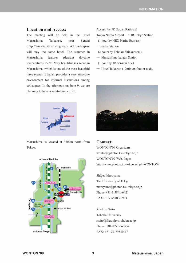
Location and Access: The meeting will be held in the Hotel
Matsushima Taikanso, near Sendai
(http://www.taikanso.co.jp/eg/). All participant
will stay the same hotel. The summer in
Matsushima features pleasant daytime
temperatures 25 ºC. Very beautiful sea scene in
Matsushima, which is one of the most beautiful
three scenes in Japan, provides a very attractive
environment for informal discussions among
colleagues. In the afternoon on June 9, we are
planning to have a sightseeing cruise.
Matsushima is located at 350km north from
Tokyo.
Access: by JR (Japan Railway)
Tokyo Narita Airport � JR Tokyo Station
(1 hour by NEX Narita Express)
�Sendai Station
(2 hours by Tohoku Shinkansen )
� Matsushima-kaigan Station
(1 hour by JR Senseki line)
� Hotel Taikanso (12min on foot or taxi).
Contact:WONTON’09 Organizers:
WONTON’09 Web. Page:
http://www.photon.t.u-tokyo.ac.jp/~WONTON/
Shigeo Maruyama
The University of Tokyo
Phone:+81-3-5841-6421
FAX:+81-3-5800-6983
Riichiro Saito
Tohoku University
Phone: +81-22-795-7754
FAX: +81-22-795-6447
INFORMATION
WONTON '09 3 Matsushima, Japan

WONTON '09 4 Matsushima, Japan
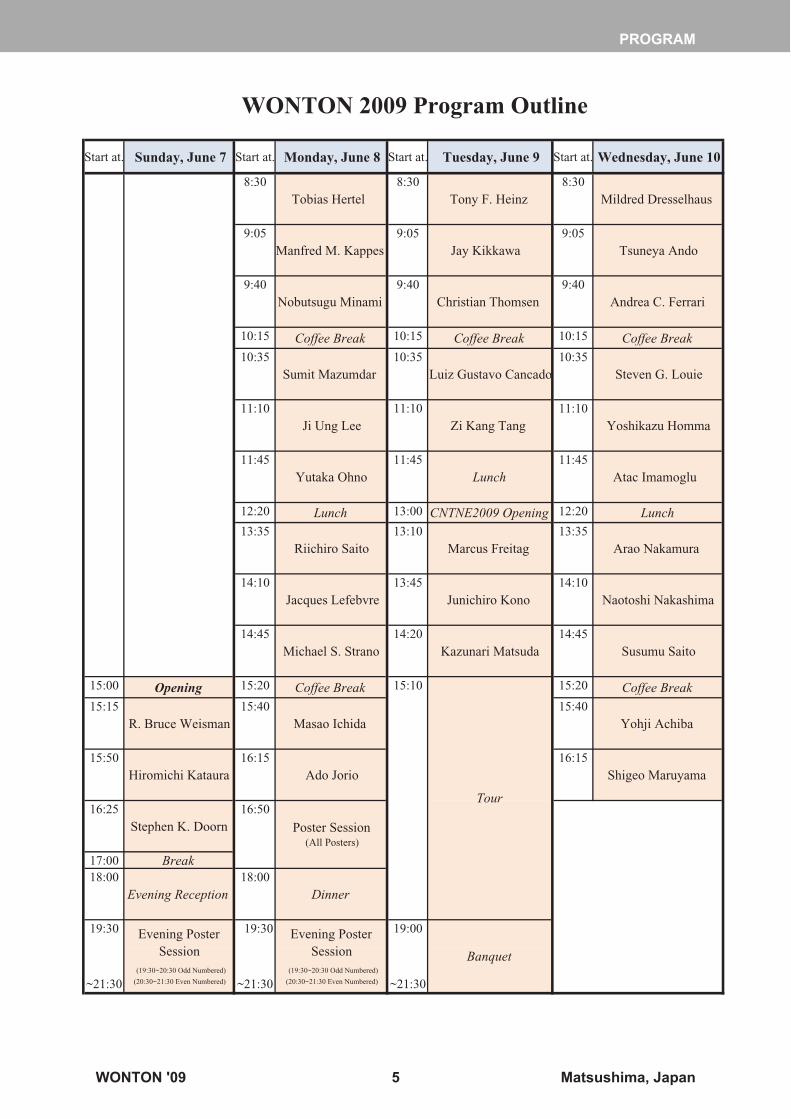
Start at. Sunday, June 7 Start at. Monday, June 8 Start at. Tuesday, June 9 Start at. Wednesday, June 10
8:30Tobias Hertel
8:30Tony F. Heinz
8:30Mildred Dresselhaus
9:05Manfred M. Kappes
9:05Jay Kikkawa
9:05Tsuneya Ando
9:40Nobutsugu Minami
9:40Christian Thomsen
9:40Andrea C. Ferrari
10:15 Coffee Break 10:15 Coffee Break 10:15 Coffee Break10:35
Sumit Mazumdar 10:35
Luiz Gustavo Cancado10:35
Steven G. Louie
11:10Ji Ung Lee
11:10Zi Kang Tang
11:10Yoshikazu Homma
11:45Yutaka Ohno
11:45Lunch
11:45Atac Imamoglu
12:20 Lunch 13:00 CNTNE2009 Opening 12:20 Lunch13:35
Riichiro Saito13:10
Marcus Freitag 13:35
Arao Nakamura
14:10Jacques Lefebvre
13:45Junichiro Kono
14:10Naotoshi Nakashima
14:45Michael S. Strano
14:20Kazunari Matsuda
14:45Susumu Saito
15:00 Opening 15:20 Coffee Break 15:20 Coffee Break15:15
R. Bruce Weisman15:40
Masao Ichida 15:40
Yohji Achiba
15:50Hiromichi Kataura
16:15Ado Jorio
16:15Shigeo Maruyama
16:25Stephen K. Doorn
17:00 Break18:00
Evening Reception18:00
Dinner
19:30 19:30 19:00
~21:30 ~21:30 ~21:30
WONTON 2009 Program Outline
Poster Session(All Posters)
16:50Tour
15:10
Evening PosterSession
(19:30~20:30 Odd Numbered)
(20:30~21:30 Even Numbered)
Evening PosterSession
(19:30~20:30 Odd Numbered)
(20:30~21:30 Even Numbered)
Banquet
PROGRAM
WONTON '09 5 Matsushima, Japan
WONTON 2009 Program
Sunday, June 7
15:00 Opening
15:15 Recent Applications of Single-Walled Carbon Nanotube FluorescenceR. Bruce Weisman
15:50 Squeezing Metallic SWCNTs from Thawed out Black Agarose
16:25 Modulation of Surfactant/Nanotube Interfacial Behavior: Enhanced Separations and SpectroscopyStephen K. Doorn, Sandip Niyogi, Crystal G. Densmore, Erik H. Haroz, Donny Magana, Junichiro Kono
17:00 Coffee Break
18:00 Evening Reception
19:30 Evening Poster Session19:30-20:30 Odd numbered posters should be presented.20:30-21:30 Even numbered posters should be presented.
Monday, June 8
8:30 When size does matter: Exciton diffusion and Brownian motion of carbon nanotubes
9:05 Photoluminescence studies and separation of single-walled carbon nanotubes
9:40
Nobutsugu Minami, Y. Futami, Said Kazaoui and Nicolas IzardNanotechnology Research Institute and Nanotube Research Center, AIST
10:15 Coffee Break
Department of Chemistry and R. E. Smalley Institute for Nanoscale Science and Technology, RiceUniversity Houston, Texas 77005 USA
Nanotechnology Research Institute (NRI), National Institute of Advanced Industrial Science andTechnology (AIST), Tsukuba, Japan, JST, CREST, Kawaguchi, Saitama, Japan, University ofTsukuba, Tsukuba Japan, Tokyo Metropolitan University, Tokyo, Japan
Chemistry Division, Los Alamos National Laboratory and Department of Electrical and ComputerEngineering, Rice University
Tobias Hertel, Thomas Ackermann, Jared Crochet, Sabine Himmelein, Dominik Stich, Larry Luer,Guglielmo Lanzani
Hiromichi Kataura, Takeshi Tanaka, Shunjiro Fujii, Daisuke Nishide, Kazuhiro Yanagi, YasumitsuMiyata, Ye Feng, Kiyoto Matsuishi, Yutaka Maniwa
Insitute for Physical Chemistry, Am Hubland, Julius-Maximilians University Wurzburg, 97076Wurzburg, Germany
Sergei Lebedkin, Oliver Kiowski, Frank Hennrich, Stefan Jester, Ninette Sturzl, Lea Burger, ZhongJin, Yan Li and Manfred M. KappesInstitute of Physical Chemistry, Universitaet Karlsruhe and Institute of Nanotechnology,Forschungszentrum Karlsruhe, Germany
Absorption, Photoluminescence and Photoconductivity of Highly Purified SemiconductingSingle-wall Carbon Nanotubes
PROGRAM
WONTON '09 6 Matsushima, Japan
10:35
S. Mazumdar, D. Psiachos and Z. WangDepartment of Physics, University of Arizona, Tucson, AZ 85721, USA
11:10 Optical Spectroscopy of Carbon Nanotube P-N DiodesJi Ung Lee
11:45
Yutaka Ohno, Atsushi Kobayashi, and Takashi MizutaniDepartment of Quantum Engineering, Nagoya University, Japan
12:20 Lunch
13:35
Riichiro SaitoTohoku University
14:10 Luminescence spectroscopy of individual SWNTs and elemental bundlesJacques Lefebvre and Paul FinnieIMS/National Research Council
14:45 Biological applications of near-infrared fluorescent sensors based on single-walled carbon nanotubes Michael S. StranoM.I.T. Dept. of Chemical Engineering
15:20 Coffee Break
15:40
Masao Ichida, Tadashi Nakano, Singo Saito, Yasumitsu Miyata, Hiromichi Kataura, and Hiroaki AndoDepartment of Physics, Konan University
16:15 Probing Disorder in Graphene with Raman Spectroscopy
16:50 Poster Session (All posters)
18:00 Dinner
19:30 Evening Poster Session19:30-20:30 Odd numbered posters should be presented.20:30-21:30 Even numbered posters should be presented.
Direct comparison of photoluminescence intensity with (n,m) abundance of single-walled carbonnanotubes
Exciton effect and phonon softening effect in the Raman spectroscopy of single wall carbonnanotubes
College of Nanoscale Science and Engineering, The University at Albany-SUNY, 255 Fuller Road,Albany, NY, USA
Nonlinear Optical Properties and Phase Relaxation Processes in Semiconducting Single-WalledCarbon Nanotubes
The Mott-Hubbard Interaction and Exciton Binding Energies in Semiconducting and MetallicSingle-Walled Carbon Nanotubes
Ado Jorio, Marcia M. Lucchese, Fernando Stavale, Erlon H. M. Ferreira, Cecilia Vilani, Rodrigo B.Capaz, Carlos. A. AcheteDepartamento de Fisica, UFMG, Belo Horizonte, MG and Divisao de Metrologia de Materiais,metro, Duque de Caxias, RJ, Brazil
PROGRAM
WONTON '09 7 Matsushima, Japan
Tuesday, June 9
8:30 Optical Spectroscopy of Single and Multilayer GrapheneTony F. HeinzDepartments of Physics and Electrical Engineering, Columbia University, New York, NY 10027, USA
9:05 Optical and Magnetic Anisotropy in Graphene OxideJay KikkawaThe University of Pennsylvania
9:40 Vibrational modes in graphene and semiconductor nanorodsChristian Thomsen
Institut fur Festkorperphysik, TU Berlin,Hardenbergstr. 36, 10623 Berlin, Germany
10:15 Coffee Break
10:35 Theory of Near-field Raman Enhancement in Carbon NanotubesLuiz Gustavo Cancado, Ado Jorio, Achim Hartschuh, E. Joselevich, and Lukas NovotnyThe Institute of Optics, University of Rochester
11:10
Z. K. Tang, J. P. Zhai, and R. Saito
11:45 Lunch
13:00 CNTNE2009 Opening (T. Mizutani)
13:10 Electrical power dissipation, phonon populations, and substrate effects in carbon nanotubes and grapheneM. FreitagIBM Watson Research Center, Yorktown Heights, NY 10598, USA
13:45 Terahertz Dynamics in Carbon Nanotubes Junichiro KonoRice University
14:20 Exciton Fine Structures and Dynamics Studied by Single Carbon Nanotube SpectroscopyKazunari MatsudaInstitute for Chemical Research, Kyoto University, Uji, Kyoto 611-0011, Japan
15:10 Tour
19:00 Banquet
Optical properties of ultra-thin single-walled carbon nanotubes aligned in the nano channels ofzeolite AEL single crystals
Department of Physics and the Institute of Nano Science & Technology, Hong Kong University ofScience and Technology, Clear Water Bay, Kowloon, Hong Kong
PROGRAM
WONTON '09 8 Matsushima, Japan
Wednesday, June 10
8:30 Our Recent Advances in Nanotube and Graphene ResearchMildred Dresselhaus and Jing KongMassachusetts Institute of Technology
9:05 Optical properties of monolayer and bilayer graphene
Tsuneya Ando1, Mikito Koshino1, and Kenichi Asano2
9:40 Raman, Photoluminescence and Saturable Absorption in GrapheneAndrea C. Ferrari Engineering Department, Cambridge University, Cambridge, UK
10:15 Coffee Break
10:35 Electronic and Optical Properties of Nanotubes, Graphene, and Graphene NanostructuresSteven G. Louie Department of Physics, University of California, Berkeley, California 94720, USA
11:10 Effects of Environment and Defects on Photoluminescence of Single Wall Carbon NanotubeYoshikazu Homma, Shohei Chiashi, Ryota Mitobe, and Kotaro Nagatsu
11:45 Quantum optics with carbon nanotubesC. Galland, A. Hoegele, and A. ImamogluETH Zurich
12:20 Lunch
13:35 Third-Order Nonlinear Optical Responsein Fullerene-Peapods
A. Nakamura1, D. Hosooka1, T. Koyama1, H. Kishida1, K. Asaka1, Y. Saito1, and T. Saito2
14:10 Direct Determination of Precise Electronic States of SWNTs Based on Soluble Carbon NanotubesNaotoshi Nakashima
14:45 Electronic and Geometrical Properties of Carbon Nanotubes: A First-Principles StudySusumu Saito
15:20 Coffee Break
Department of Physics, Tokyo University of Science, 1-3 Kagurazaka, Shinjuku-ku, Tokyo 162-8601,Japan
Department of Physics, Tokyo Institute of Technology, 2-12-1 Oh-okayama, Meguro-ku, Tokyo 152-8551, Japan
1 Department of Physics, Tokyo Institute of Technology, 2–12–1 Ookayama, Meguro-ku, Tokyo 152-8551, Japan2 Department of Physics, Osaka University, 1–1 Machikaneyama, Toyonaka 560-0043, Japan
Department of Applied Chemistry, Graduate School of Engineering, Kyushu University, Fukuoka819-0395 Japan
1 Department of Applied Physics, Nagoya University Furo-cho, Chikusaku, Nagoya 464-8603 Japan,2 Research Center for Advanced Carbon Materials, AIST, 1-1-1 Higashi, Tsukuba, 305-8565, Japan
PROGRAM
WONTON '09 9 Matsushima, Japan

15:40 Production of (5,4) and (6,4) Enriched Single-Walled Carbon Nanotubes Grown Using a Platinum Catalyst
Naoko Takamizu1,Keisuke Urata1,Toshiya Okazaki2,and Yohji Achiba1
16:15 Spectral features due to dark exciton in photoluminescence map of single-walled carbon nanotubes
Shigeo Maruyama1, Yuhei Miyauchi2 and Yoichi Murakami 3
1 Department of Mechanical Engineering, The University of Tokyo, 7-3-1 Hongo, Bunkyo-ku, Tokyo
113-8656, Japan, 2 Institute for Chemical Research, Kyoto University, Uji, Kyoto 611-0011,
Japan, 3 Global Edge Institute, Tokyo Institute of Technology, 2-12-1 Ookayama, Meguro-ku, Tokyo152-8550, Japan
1 Department of Chemistry, Tokyo Metropolitan University, Tokyo 192-0397,Japan2 Nanotube Research Center, AIST, Tsukuba 305-8568, Japan
PROGRAM
WONTON '09 10 Matsushima, Japan
Poster Presentations
All posters will be displayed from opening on 7th through lunch time on 10th.For Evening Poster Sessions, during 19:30-21:30 in June 7 and 8, Odd-numbered posters should be presented during 19:30-20:30 and even-numbered posters should be presented during 20:30-21:30 for better access to the presenter.
P1 Enrichment of Armchair Carbon Nanotubes via Density Gradient Ultracentrifugation: Raman Spectroscopy Evidence
P2 Quantitative Purity Evaluation of Single-Wall Carbon Nanotubes using Resonance Raman SpectroscopyDaisuke Nishide, Yasumitsu Miyata, Kazuhiro Yanagi, Takeshi Tanaka, and Hiromichi Kataura
P3 Optical Active Single-Walled Carbon NanotubesNaoki Komatsu, Xiaobin Peng, Feng Wang, Ajoy Bauri, A. F. M. M. Rahman, Takahide Kimura, and Atsuhiro Osuka
P4 Optical characterization of Length-Separated DNA-Wrapped Double-Wall Carbon NanotubesYuki Asada, Shota Kuwahara, Toshiki Sugai, Ryo Kitaura, and Hisanori Shinohara
P5 Resonance Raman Spectra of Optical Purified (6,5) Nanotubes Sorted by Density Gradient UltracentrifugationPei Zhao, Theerapol Thurakitseree, Erik Einarsson, Junichiro Shiomi, Shigeo Maruyama
P6
Romain Fleurier, Jean-Sebastien Lauret, Emmanuel Flahaut, Annick Loiseau
P7 Polarized Raman spectroscopy on vertically aligned single-walled carbon nanotubes Zhengyi Zhang, Yoichi Murakami, Erik Einarsson, Yuhei Miyauchi and Shigeo Maruyama
P8 High-Precision Selective Deposition of Catalyst for Facile Localized Growth of Single Walled Carbon NanotubesRong Xiang, Tianzhun Wu, Erik Einarsson, Yuji Suzuki, Yoichi Murakami, Junichiro Shiomi, Shigeo Maruyama
P9
P10 Effects of Bundling and Diameter on the UV Optical Absorption of Single-Wall Carbon NanotubesTakeshi Saito, Shigekazu Ohmori, Bikau Shukla, Motoo Yumura and Sumio Iijima
P11 Fermi energy dependence of radial breathing mode in metallic single-wall carbon nanotubesJin Sung Park, Kenich Sasaki, Riichiro Saito, Gene Dressselhaus, Mildred S. Dresselhaus
P12 Exciton energy Kataura plot and excitonic effect of single wall carbon nanotubesKentaro Sato, Riichiro Saito and Shigeo Maruyama
P13 Pressure-assisted tip-enhanced Raman imaging of carbon nanotubesat the spatial resolution of a few nanometresTaka-aki Yano, Prabhat Verma, Yuika Saito, Taro Ichimura and Satoshi Kawta
P14 Resonance Raman scattering of hole-doped metallic and semiconducting carbon nanotubesYasumitsu Miyata, Kazuhiro Yanagi, Yutaka Maniwa, Hisanori Shinohara and Hiromichi Kataura
P15 Coherent Phonon Dynamics in Highly Aligned Single-Walled Carbon NanotubesLayla G. Booshehri, Erik H. Haroz, Junichiro Kono, Cary L. Pint, Robert H. Hauge, Yong-sik Lim, Ji-Hee Kim, Ki-Ju Yee
P16 Photoluminescence Observation of Water Encapsulation in an individual Single-walled Carbon NanotubeShohei Chiashi, Tataki Hanashima, Ryota Mitobe, Yoshikazu Homma
P17 Intrinsic and Extrinsic Factors which Affects the Optical Properties of Individual Single-Walled Carbon Nanotubes Juan G. Duque, Stephen Door, Howard K. Schmidt and Matteo Pasquali Laurent Cognet and Brahim Lounis
P18 Electrochemistry and Self-Assembly of Complex Single-Walled Carbon Nanotube (SWNT) NanostructuresJuan G. Duque, Laurent Cognet, Howard K. Schmidt, Matteo Pasquali
Erik H. Haroz, William D. Rice, Benjamin Y. Lu, Robert H. Hauge, Saunab Ghosh, R. Bruce Weisman, Pavel Nikolaev,Sivaram Arepalli, Donny Magana, Stephen K. Doorn, and Junichiro Kono
Raman and optical spectroscopic analysis of single walled carbon nanotubes synthesized by an industrial scale aerosolreactor
Diameter distribution analysis of sorted double wall carbon nanotubes by optical absorption spectroscopy and electrontransmission microscopy.
Ying Tian, Albert G Nasibulin, Hua Jiang, Timur Nikitin, Brad Aitchison, Jan V Pfaler, Leonid Khriachtchev, Jussi O Sarkkinen,David P Brown, Esko I Kauppinen
PROGRAM
WONTON '09 11 Matsushima, Japan
P19 SEM Observation Effect on Photoluminescence Spectra from Single-Walled Carbon NanotubesKotaro Nagatsu, Tomohito Chokan, Takeshi Kitajo, Shohei Chiashi, Yoshikazu Homma
P20 Fast Band-Gap Tuning of Carbon Nanotube with Repetitious Uniaxial StrainHideyuki Maki and Tetsuya Sato
P21 An Optical Study of a Single Carbon NanotubeXu Wang, M. Hadjipanayi, R. J. Nicholas and R. A. Taylor
P22 Photoluminescence saturation in an air-suspended SWCNTY.-F. Xiao, T.Q. Nhan, M.W.B. Wilson, and James M. Fraser
P23 Symmetry-Induced Exciton Distribution between the Bright and Dark States in Single Carbon NanotubesRyusuke Matsunaga, Kazunari Matsuda, and Yoshihiko Kanemitsu
P24 Exciton Dynamics in Carbon Nanotubes and Nonlinear Dependence of Photoluminescence Intensity on Pump PowerMaria Hilczer and M. Tachiya
P25 Exciton Dephasing Dynamics in Single-Walled Carbon NanotubesM. W. Graham, Y.-Z. Ma, A. A. Green, M. C. Hersam and G. R. Fleming
P26 Exciton Radiative Lifetimes and Coherence Lengths in Single-Walled Carbon NanotubesYuhei Miyauchi, Ryusuke Matsunaga, Hideki Hirori, Kazunari Matsuda, and Yoshihiko Kanemitsu
P27 Excitons in carbon nanotube within effective-mass approximationTsuneya Ando and Seiji Uryu
P28 Inter-Valley Mixing of Carbon Nanotube Excitons by a Short-Range ImpurityYuh Tomio and Hidekatsu Suzuura
P29 Theory of 1D Exciton and its Application to SWNTSeiji Sakoda and Madoka Tokumoto
P30 Reflectance spectra of individual metallic single walled carbon nanotubes.Hualing Zeng, Hongbo Zhao, Fu-Chun Zhang, and Xiaodong Cui
P31 Magneto-optical Spectroscopy of Metallic Single-Walled Carbon NanotubesT. A. Searles, J. Kono, J. A. Fagan, Erik K. Hobbie, Y. Imanaka
P32 Anisotropic Terahertz Response of Aligned Carbon Nanotubes
P33 Finite-length effects on optical absorption in metallic carbon nanotubesTakeshi Nakanishi and Tsuneya Ando
P34 Resonant Optical Forces for Nanotube Aggregation in SolutionThomas Rodgers, Satoru Shoji, and Satoshi Kawata
P35 Molecular physisorption at the groove and interior of single-walled carbon nanotubesS. Iwata, S. Ogura, S. Lee, K. Fukutani, Y. Sato and K. Tohji
P36 Efficient dissociation of carbon nanotube excitons in organic semiconductor / carbon nanotube heterojunctions forphotovoltaics and ultrabroadband photodetectionMichael S. Arnold, Jeramy D. Zimmerman, Christopher K. Renshaw, Xin Xu1, Richard R. Lunt, Christine M. Austin, andStephen R. Forrest
Lei Ren, Layla G. Booshehri, William D. Rice, Xiangfeng Wang, David J. Hilton, Junichiro Kono, Cary L. Pint, Robert H. Hauge,Aleksander K. Wojcik, Alexey A. Belyanin, Yoshiaki Takemoto, Kei Takeya, Iwao Kawayama , and Masayoshi Tonouchi
PROGRAM
WONTON '09 12 Matsushima, Japan

INVITED TALK
June 7, Sunday
AbstractsInvited Speakers
WONTON '09 13 Matsushima, Japan

WONTON '09 14 Matsushima, Japan
Recent Applications of Single-Walled Carbon Nanotube Fluorescence
R. Bruce Weisman Department of Chemistry and R. E. Smalley Institute for Nanoscale Science and Technology
Rice University Houston, Texas 77005 USA
The intrinsic near-IR fluorescence of semiconducting single-walled carbon nanotubes (SWCNTs) provides a powerful tool for a range of basic and applied investigations. One particularly valuable approach involves the use of near-IR microscopy to acquire images and spectra of individual SWCNTs. We have used this approach to extend our calibrated measurements of absolute fluorescence action cross sections to additional (n,m) species not previously reported. These fluorescence action cross sections are the products of E22 peak absorptivity times fluorescence quantum yield for pristine SWCNTs in aqueous SDBS suspension. The data reveal strong structure-dependent patterns for smaller diameter nanotubes, from which general empirical patterns can be deduced. The results provide calibration factors for deducing (n,m) concentration distributions from bulk fluorimetric measurements. In another project, an efficient new method has been developed for measuring SWCNT length distributions. Dilute samples in liquid suspension are imaged by near-IR fluorescence videomicroscopy at frame rates high enough to resolve the Brownian motions of the nanotubes. Custom image analysis software then identifies all of the SWCNTs in the frame, tracks their individual trajectories, deduces the corresponding translational diffusion coefficients, converts diffusion coefficients into lengths, and compiles the histogram of nanotube lengths. Data acquisition and analysis in this method are much quicker than for AFM length analysis. In the third application, a variety of bulk and single-particle methods have been used to investigate the apparent inner shell near-IR emission from samples of DWCNTs. We have studied the spectroscopy, chemical quenching, mechanical rigidity, density, and TEM structures of the near-IR emitters in DWCNT samples. The findings show that genuine inner shell fluorescence from DWCNTs is weaker than SWCNT fluorescence by a factor of at least 10,000, and that the observed near-IR emission is attributable to the presence of residual SWCNTs.
INVITED TALK June 7, Sunday
WONTON '09 15 Matsushima, Japan
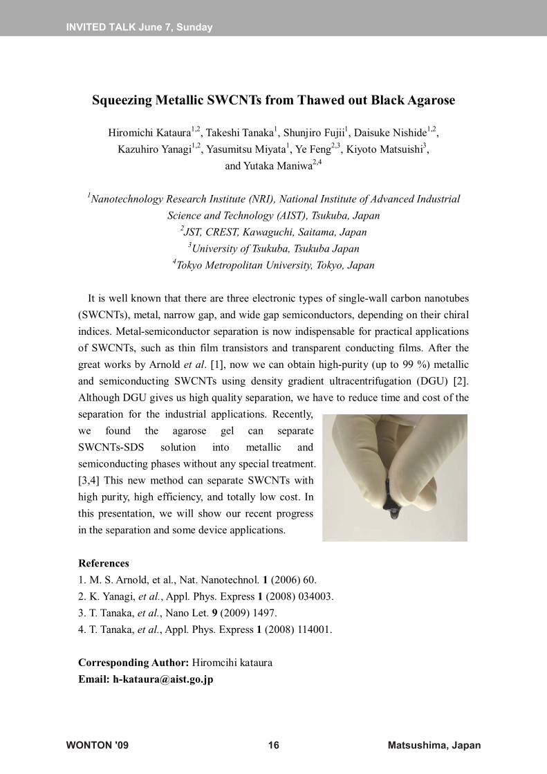
Squeezing Metallic SWCNTs from Thawed out Black Agarose
Hiromichi Kataura1,2, Takeshi Tanaka1, Shunjiro Fujii1, Daisuke Nishide1,2,
Kazuhiro Yanagi1,2, Yasumitsu Miyata1, Ye Feng2,3, Kiyoto Matsuishi3,
and Yutaka Maniwa2,4
1Nanotechnology Research Institute (NRI), National Institute of Advanced Industrial
Science and Technology (AIST), Tsukuba, Japan2JST, CREST, Kawaguchi, Saitama, Japan
3University of Tsukuba, Tsukuba Japan4Tokyo Metropolitan University, Tokyo, Japan
It is well known that there are three electronic types of single-wall carbon nanotubes
(SWCNTs), metal, narrow gap, and wide gap semiconductors, depending on their chiral
indices. Metal-semiconductor separation is now indispensable for practical applications
of SWCNTs, such as thin film transistors and transparent conducting films. After the
great works by Arnold et al. [1], now we can obtain high-purity (up to 99 %) metallic
and semiconducting SWCNTs using density gradient ultracentrifugation (DGU) [2].
Although DGU gives us high quality separation, we have to reduce time and cost of the
separation for the industrial applications. Recently,
we found the agarose gel can separate
SWCNTs-SDS solution into metallic and
semiconducting phases without any special treatment.
[3,4] This new method can separate SWCNTs with
high purity, high efficiency, and totally low cost. In
this presentation, we will show our recent progress
in the separation and some device applications.
References
1. M. S. Arnold, et al., Nat. Nanotechnol. 1 (2006) 60.
2. K. Yanagi, et al., Appl. Phys. Express 1 (2008) 034003.
3. T. Tanaka, et al., Nano Let. 9 (2009) 1497.
4. T. Tanaka, et al., Appl. Phys. Express 1 (2008) 114001.
Corresponding Author: Hiromcihi kataura
Email: [email protected]
INVITED TALK June 7, Sunday
WONTON '09 16 Matsushima, Japan
Modulation of Surfactant/Nanotube Interfacial Behavior: Enhanced Separations and Spectroscopy
Stephen K. Doorn1, Sandip Niyogi1, Crystal G. Densmore1, Erik H. Haroz2, Donny
Magana1, Junichiro Kono2
1Chemistry Division, Los Alamos National Laboratory,
C-PCS, MS-J563, Los Alamos, NM 87545, U.S.A. 2Department of Electrical and Computer Engineering, Rice University, Houston, TX
77251, U.S.A.
Current advances in density-based separations of carbon nanotubes rely on modulation
of surfactant interactions at the nanotube surface. We have studied how these
interactions can be tuned via addition of electrolyte to surfactant suspensions of
nanotubes. Addition of metal chloride salts will selectively aggregate nanotubes in a
diameter-dependent fashion [1]. Use of salt concentrations below this aggregation
threshold can act to enhance the density differences between nanotubes of similar
diameter and/or metallicity. Use of this phenomenon to separate nanotubes into highly
enriched metallic and semiconductor fractions in a diameter-dependent fashion will be
discussed [2]. It will also be shown how electrolyte modulation of photoluminescence
behavior, paired with the separations results, can act as a probe of the surfactant
structure at the nanotube surface. Additionally, examples of how access to such
enriched samples enables new fundamental measurements will be discussed. In
particular, results will be presented that demonstrate generalized G-band behavior in
armchair metallic nanotubes. Recent UV-Raman measurements of enriched samples
will also be presented.
References
1. S. Niyogi, S. Boukhalfa, B. C. Satishkumar, T. J. McDonald, M. J. Heben, S. K.
Doorn, J. Am. Chem. Soc., 129, 1898 (2007).
2. S. Niyogi, C. G. Densmore, S. K. Doorn, J. Am. Chem. Soc., 131, 1144 (2009).
Corresponding Author: Stephen K. Doorn
Email: [email protected]
INVITED TALK June 7, Sunday
WONTON '09 17 Matsushima, Japan

INVITED TALK June 7, Sunday
WONTON '09 18 Matsushima, Japan

WONTON '09 19 Matsushima, Japan

WONTON '09 20 Matsushima, Japan
When size does matter: exciton diffusion and Brownian motion of carbon nanotubes
Tobias Hertel1, Thomas Ackermann1, Jared Crochet1, Sabine Himmelein1, Dominik
Stich1, Larry Lüer2, Guglielmo Lanzani3
1Insitute for Physical Chemistry, Am Hubland, Julius-Maximilians University Würzburg, 97076 Würzburg, Germany
2National Laboratory for Ultrafast and Ultraintense Optical Science, INFM-CNR, Dipartimento di Fisica, Politecnico di Milano, Italy
3Italian Institute of Technology and Dipartimento di Fisica, Politecnico di Milano, P.za L. da Vinci 32, 20133 Milano, Italy
We have studied exciton diffusion in SWNTs and carbon nanotube diffusion in aqueous
environments using optical and colloidal techniques for the characterization of excited
state- and particle kinetics. The character of exciton diffusion in semiconducting carbon
nanotubes is governed by the mean electron-hole separation, which has been determined
experimentally using femtosecond time-resolved pump-probe spectroscopy. The finite
length of tubes and the electronic structure of their ends likewise have an effect on
exciton dynamics by providing additional pathways for non-radiative decay and by
limiting the range that excitons can explore before decaying non-radiatively. Finite tube
length has moreover been found to severely limit the achievable photoluminescence
quantum yields for tubes shorter than about 100 nm. The resulting length dependence of
photoluminescence quantum yields allows a determination of exciton diffusion lengths.
In combination with time-resolved photoluminescence studies this can be used to infer
exciton diffusion constants which are here found to be on the order of 0.1 cm2 s-1. The
effect of the environment on non-radiative exciton decay has been studied by
systematically varying the surfactant coating. In addition we discuss the outcome of
recent efforts with the preparation of length selected SWNTs using zonal fractionation
in density gradients and asymmetric-flow field-flow fractionation. Nanotube diffusion
and its dependence on tube length plays a crucial role for both these techniques and is
studied by a combination of fluorescence correlation microscopy and zonal
fractionation.
Corresponding Author: Tobias Hertel
Email: [email protected]
INVITED TALK June 8, Monday
WONTON '09 21 Matsushima, Japan
Photoluminescence studies and separation ofsingle-walled carbon nanotubes
Sergei Lebedkin 1, Oliver Kiowski 1,2, Frank Hennrich 1, Stefan Jester 1,2,
Ninette Stürzl 1,2, Lea Burger1,2, Zhong Jin 3, Yan Li 3, and Manfred M. Kappes 1,2
1Forschungszentrum Karlsruhe, Institut für Nanotechnologie,
D-76021 Karlsruhe, Germany 2Institut für Physikalische Chemie, Universität Karlsruhe,
D-76128 Karlsruhe, Germany 3 Beijing National Laboratory for Molecular Sciences, College of Chemistry and
Molecular Engineering, Peking University, Bejing 100871,China
We will present our recent results on the photoluminescence (PL) spectroscopy and
imaging of semiconducting single-walled carbon nanotubes (SWNTs). These include
studies of individual, millimeter-long nanotubes grown by chemical vapor deposition on
pre-patterned silicon substrates and characterized by PL before and after micro-
manipulation with an atomic force microscope. PL provides information about the local
nanotube surroundings (air-suspended vs. on-silicon nanotube sections), the axial and
torsional strain generated in the nanotube, as well as shows characteristic changes at a
nanotube rupture site. Complimentary to photophysical studies on individual nanotubes
we have also carried out ensemble measurements of SWNT dispersions which are highly
enriched in a specific nanotube species. Nearly monodisperse (up to ~90% purity)
samples of several semiconducting nanotube species could be obtained by using a
relatively simple and readily scalable procedure based on dispersion in non-polar
solvents/organic polymers. Finally, we have found that SWNTs are efficient and
extremely robust quenchers of singlet oxygen.
Corresponding Author: Manfred M. Kappes
Email: [email protected]
INVITED TALK June 8, Monday
WONTON '09 22 Matsushima, Japan
Absorption, Photoluminescence and Photoconductivity of Highly Purified Semiconducting Single-wall Carbon Nanotubes
Nobutsugu Minami1, Y. Futami1, Said Kazaoui2 and Nicolas Izard 2
1Nanotechnology Research Institute and 2Nanotube Research Center
National Institute of Advanced Industrial Science and Technology
AIST Tsukuba Central 5, Tsukuba, Ibaraki 305-8565, Japan
Highly pure semiconducting single-wall carbon nanotubes (s-SWNTs) with selective
chiralities can be extracted by the use of polyfluorene (PFO) as a dispersant dissolved in
toluene [1,2], yielding sharp and well-resolved optical spectra. Moreover, the absorption
background supposedly ascribed to carbonaceous impurities can be considerably
suppressed. Thus simplified spectral shape has expanded the applicability of optical
spectroscopy to the study of electronic processes in s-SWNTs. Here we applied
absorption (Abs), photoluminescence (PL), and photoconduction spectroscopy for the
study of various properties of selectively extracted s-SWNT. We stress that the
successful fabrication of highly pure s-SWNT thin films has enabled the straightforward
measurement and analysis of the photoconductivity with minimal disturbance due to
dark conduction in residual metallic SWNTs.
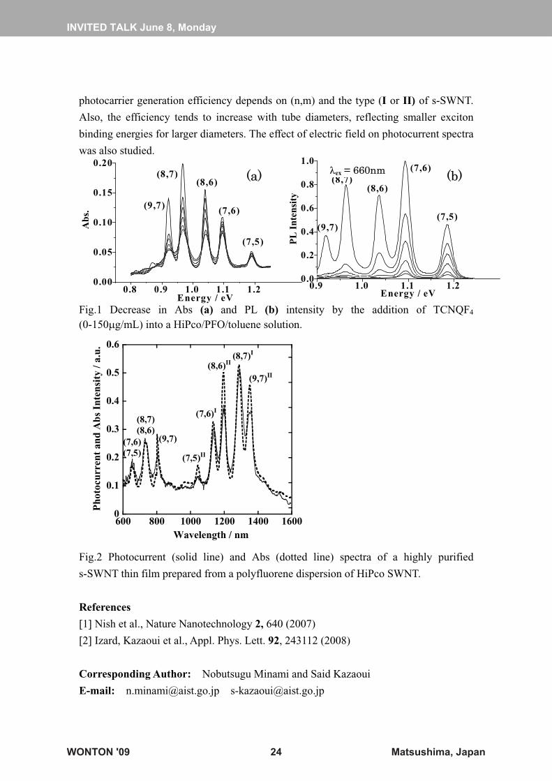
Figure 1 shows changes in Abs and PL spectra induced by the addition of
tetrafluorotetracyanoquinodimethane (TCNQF4), a p-dopant, into a HiPco/PFO/toluene
solution. It is remarkable that, for Abs, isosbestic points are clearly observed with the
increase in TCNQF4 concentration and only the low-energy (9,7) peak shows a
considerable decrease in Abs intensity. On the other hand, PL decrease by doping is
much larger for all chiral indexes (n, m), implying that the underlying mechanisms are
different. Stern-Volmer plot of PL quenching revealed good correlation between the
position of LUMO and a Stern-Volmer constant for each (n, m). Implications of these
results will be discussed in relation to charge transfer between TCNQF4 and
ground/excited states in s-SWNTs.
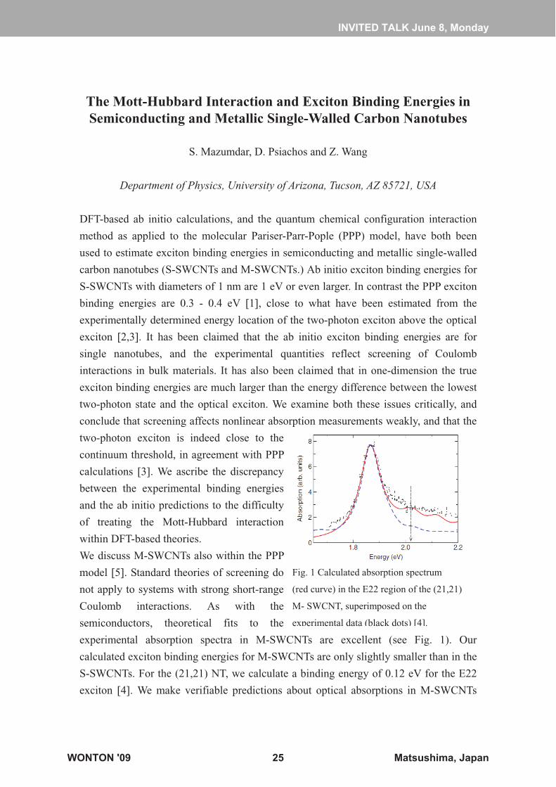
Photocurrent and Abs spectra are compared in Fig. 2 for a thin film prepared from
highly purified s-SWNT dispersion. The observation of clearly separated peaks each
assigned to different chiral indexes (n, m) has made it possible to extract information
about the photoconduction process. Specifically, it can be seen that the relative
INVITED TALK June 8, Monday
WONTON '09 23 Matsushima, Japan
photocarrier generation efficiency depends on (n,m) and the type (I or II) of s-SWNT.
Also, the efficiency tends to increase with tube diameters, reflecting smaller exciton
binding energies for larger diameters. The effect of electric field on photocurrent spectra
was also studied.
Fig.1 Decrease in Abs (a) and PL (b) intensity by the addition of TCNQF4
(0-150�g/mL) into a HiPco/PFO/toluene solution.
0.9 1.0 1.1 1.20.0
0.2
0.4
0.6
0.8
1.0
(8,7)(8,6)
(7,6)
(7,5)(9,7)
PL
Int
ensi
tyEnergy / eV
(b)�ex�= 660nm
0.8 0.9 1.0 1.1 1.20.00
0.05
0.10
0.15
0.20
(7,6)
(8,6)
(7,5)
(8,7)
(9,7)
Abs
.
Energy / eV
(a)
0
0.1
0.2
0.3
0.4
0.5
0.6
600 800 1000 1200 1400 1600
Pho
tocu
rren
t an
d A
bs I
nten
sity
/ a.
u.
Wavelength / nm
(9,7)II
(7,6)I
(8,6)II(8,7)I
(7,5)II
(8,7)(8,6)
(7,6)(7,5)
(9,7)
Fig.2 Photocurrent (solid line) and Abs (dotted line) spectra of a highly purified
s-SWNT thin film prepared from a polyfluorene dispersion of HiPco SWNT.
References
[1] Nish et al., Nature Nanotechnology 2, 640 (2007)
[2] Izard, Kazaoui et al., Appl. Phys. Lett. 92, 243112 (2008)
Corresponding Author: Nobutsugu Minami and Said Kazaoui
E-mail: [email protected] [email protected]
INVITED TALK June 8, Monday
WONTON '09 24 Matsushima, Japan
The Mott-Hubbard Interaction and Exciton Binding Energies in Semiconducting and Metallic Single-Walled Carbon Nanotubes
S. Mazumdar, D. Psiachos and Z. Wang
Department of Physics, University of Arizona, Tucson, AZ 85721, USA
DFT-based ab initio calculations, and the quantum chemical configuration interaction
method as applied to the molecular Pariser-Parr-Pople (PPP) model, have both been
used to estimate exciton binding energies in semiconducting and metallic single-walled
carbon nanotubes (S-SWCNTs and M-SWCNTs.) Ab initio exciton binding energies for
S-SWCNTs with diameters of 1 nm are 1 eV or even larger. In contrast the PPP exciton
binding energies are 0.3 - 0.4 eV [1], close to what have been estimated from the
experimentally determined energy location of the two-photon exciton above the optical
exciton [2,3]. It has been claimed that the ab initio exciton binding energies are for
single nanotubes, and the experimental quantities reflect screening of Coulomb
interactions in bulk materials. It has also been claimed that in one-dimension the true
exciton binding energies are much larger than the energy difference between the lowest
two-photon state and the optical exciton. We examine both these issues critically, and
conclude that screening affects nonlinear absorption measurements weakly, and that the
two-photon exciton is indeed close to the
continuum threshold, in agreement with PPP
calculations [3]. We ascribe the discrepancy
between the experimental binding energies
and the ab initio predictions to the difficulty
of treating the Mott-Hubbard interaction
within DFT-based theories.
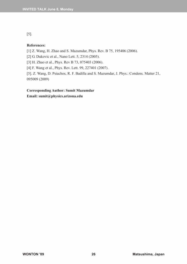
We discuss M-SWCNTs also within the PPP
model [5]. Standard theories of screening do
not apply to systems with strong short-range
Coulomb interactions. As with the
semiconductors, theoretical fits to the
experimental absorption spectra in M-SWCNTs are excellent (see Fig. 1). Our
calculated exciton binding energies for M-SWCNTs are only slightly smaller than in the
S-SWCNTs. For the (21,21) NT, we calculate a binding energy of 0.12 eV for the E22
exciton [4]. We make verifiable predictions about optical absorptions in M-SWCNTs
Fig. 1 Calculated absorption spectrum
(red curve) in the E22 region of the (21,21)
M- SWCNT, superimposed on the
experimental data (black dots) [4].
INVITED TALK June 8, Monday
WONTON '09 25 Matsushima, Japan
[5].
References:
[1] Z. Wang, H. Zhao and S. Mazumdar, Phys. Rev. B 75, 195406 (2006).
[2] G. Dukovic et al., Nano Lett. 5, 2314 (2005).
[3] H. Zhao et al., Phys. Rev B 73, 075403 (2006).
[4] F. Wang et al., Phys. Rev. Lett. 99, 227401 (2007).
[5]. Z. Wang, D. Psiachos, R. F. Badilla and S. Mazumdar, J. Phys.: Condens. Matter 21,
095009 (2009)
Corresponding Author: Sumit Mazumdar
Email: [email protected]
INVITED TALK June 8, Monday
WONTON '09 26 Matsushima, Japan
Optical Spectroscopy of Carbon Nanotube P-N Diodes
Ji Ung Lee1
1College of Nanoscale Science and Engineering, The University at Albany-SUNY, 255 Fuller Road, Albany, NY, USA
The p-n diode is an ideal device for probing optical properties of semiconductors.
Here, we demonstrate that p-n diodes formed along individual nanotubes can probe the
excited states of single-walled carbon nanotubes. The p-n diodes are formed using a
split gate structure that electrostatically dopes the two ends of a single nanotube.
These devices are fabricated at CNSE’s advanced 300mm wafer processing facility
which allows large numbers of devices to be fabricated on a single die. This allows a
large design variation to be examined, including devices with additional gates for
further doping control.
In the photocurrent spectroscopy, a series of peaks are observed. These correspond to
exciton and exciton photon peaks, for the lowest and higher sub-bands, providing
specific signature of the nanotube chirality. Here, we will report on the observation of
two new sets of fine structures. For suspended nanotubes, a fine-structure associated
with the lowest exciton peaks can we seen. For those resting on a SiO2 surface, a
large set of narrow (~2meV) peaks can be seen. We will discuss the origin of these
peaks and, when applicable, discuss them in the context of the diode current-voltage
characteristics.
Corresponding Author: Ji Ung Lee
Email: [email protected]
INVITED TALK June 8, Monday
WONTON '09 27 Matsushima, Japan
Direct comparison of photoluminescence intensity with (n,m)abundance of single-walled carbon nanotubes
Yutaka Ohno, Atsushi Kobayashi, and Takashi Mizutani
Department of Quantum Engineering, Nagoya University,
Furo-cho, Chikusa-ku, Nagoya 464-8603
The abundances of single-walled carbon nanotubes (SWNTs) grown on a
periodic trench structure [1] have been investigated for 20 species by counting the
number of luminous spots by means of the micro-photoluminescence (PL) spatial
distribution measurements. The abundance was estimated from the length and the
number of SWNTs. We obtained featureless (n,m) distributions of the length and
number of SWNTs in the growth condition used in this study. From the direct
comparison of photoluminescence intensity with (n,m) abundance, the (n,m) dependence
of PL efficiency has been investigated experimentally. The PL efficiencies of type-I
[2n+m mod 3 = 1] were slightly higher than those of type-II [2n+m mod 3 = 1], and the
higher PL efficiency was obtained in the smaller diameter. In addition, the PL efficiency
also seemed to follow the energy gap law [2], indicating that the nonradiative relaxation
attributed to G-band phonon was dominant in the relaxation process from the first
excited state of exciton to the ground state, possibly via nonradiative recombination
centers.
References
1. Y. Ohno et al., Phys. Rev. B 73, 235427 (2006).
2. D. A. Tsyboulski et al., Nano Lett. 7, 3080 (2007).
Corresponding Author Email: [email protected]
INVITED TALK June 8, Monday
WONTON '09 28 Matsushima, Japan
Exciton effect and phonon softening effect in the Ramanspectroscopy of single wall carbon nanotubes
Riichiro Saito1
2Department of Physics, Tohoku University, Sendai 980-8578, Japan
Recent Raman measurements of single wall carbon nanotubes (SWNTs) have been
provided the detailed Raman spectra as function of the surrounding materials or the
Fermi energy. The modifications of such conditions change the dielectric response of
the exciton states of SWNTs and phonon self energy for the electron-phonon interaction,
which are known as the environmental effect and the Kohn anomaly effect, respectively.
By comparing with the experiments, we can discuss physics of the exciton and phonons
of SWNTs. For the environmental effect, the dielectric response for an exciton is
important for determining the transition energies as a function of SWNT diameter
(exciton Kataura plot), which is a subject of the talk [1]. Electro-chemical doping makes
it possible to change the Fermi energy in which each Raman active phonon has a finite
life time as a function of the Fermi energy because of the electron-phonon interaction.
When we discuss the Raman intensity, two kinds of the life time in a Raman process
should be considered. One is the life time for the photo-excited carrier to emit a phonon,
which is relevant to the resonance widow in the Raman excitation profile. Another life
time is the phonon coherent time in which the vibration of phonon can be defined which
is relevant to the spectra width of the Raman spectra. In the presence of electron-phonon
(exciton-phonon) interaction, the virtual excitation of e-h pair in the metallic energy sub
band makes either softening or hardening of phonon frequencies in the metallic SWNTs.
We show in this presentation that the Kohn anomaly effect generally occurs for all
Raman active modes which show different chiral angle dependence [2]. Analytical
expression of the electron-phonon interaction can reproduce the specific measurement
of the single nanotube spectroscopy as a function of the Fermi energy.
References
1. P. T. Araujo et al., unpublished.
2. K. Sasaki, et al., Phys. Rev. B, 78, 235405 (2008). Related references therein.
Corresponding Author: Riichiro Saito
Email: [email protected]
INVITED TALK June 8, Monday
WONTON '09 29 Matsushima, Japan
Luminescence spectroscopy of individual SWNTs and elemental bundles
Jacques Lefebvre and Paul Finnie
Institute for MicrostructuralSciences, National Research Council
Ottawa, Ontario, Canada K1A 0R6
We have demonstrated that photoluminescence imaging at the single SWNT level is a
powerful tool to access detailed information about SWNT optical properties.
Luminescence from isolated SWNTs shows high spatial uniformity and high quantum
efficiency [1] and the excitonic excited states spectrum has been observed [2, 3]. In this
presentation, I will review our photoluminescence excitation studies that led to a
definite assignment of new spectral features to exciton excited states of transverse and
longitudinal nature [2, 3]. The binding energy for the lowest bright exciton and its
diameter dependence is determined and the self-energy correction can also be estimated.
Building on the known spectral signature of individually isolated SWNTs, I will report
on recent studies of elemental bundles made of two, three and even four semiconducting
SWNTs. When SWNT components of bundles are of different lengths we separately
resolve bundled and unbundled sections both spatially and spectrally (in PL as well as in
PLE mapping).[4] In agreement with previous near field and ensemble measurements,
exciton energy transfer is observed from donor to acceptor nanotube. However, the
reverse process of transfer from acceptor to donor is also important. The persistent
luminescence of donor SWNTs is understood as a consequence of thermalization of
excitons within bundles.
References
1. Lefebvre, J.; Austing, D. G.; Bond, J.; Finnie, P. Photoluminescence imaging of
suspended single-walled carbon nanotubes. Nano Lett. 2006, 6, 1603-1608.
2. Lefebvre, J.; Finnie, P. Polarized photoluminescence excitation spectroscopy of
single-walled carbon nanotubes. Phys. Rev. Lett. 2007, 98, 167406.
3. Lefebvre, J.; Finnie, P. Excited excitonic states in single-walled carbon nanotubes.
Nano Lett. 2008, 8, 1890-5.
4 Lefebvre, J.; Finnie, P. to be published.
Corresponding Author: Jacques Lefebvre
Email: [email protected]
INVITED TALK June 8, Monday
WONTON '09 30 Matsushima, Japan
Title: Biological applications of near infrared fluorescent sensors based on single walled carbon nanotubes
� ��������������� ���������� ����������� �����������
������������������������������������������������� ��������������� �
������������������������������� ��������������� �������!�
���������������������������������������"#� �����������������
������������������������ ��� ������ ��������������� ������������
���� ��� ���������������������� ��������������������������������
�����������������������������������������������������������������
���������������� ������������������������������������������
�������������������������������� ����������� ������������!���
������������ ������������������������������������ ������
������������������������������������������������ �������������
� ���������������������$�����$������������������ ����%��������
�"&�'�'���� ����������� �������������������������$���������#(��
��������������������������������������������������������������
� ������������� ����������������������������������$�� ������
����� �������$����)���������������������������������������
��������������������*���� ��+�����,�����#������*+,#����������
���������-�&.(.�������������� �����������������������������
������������������������������������� �����&.(.���� ����
������������������ ��� ����%����������������������������
����������������������������������������� ����� ��������
$����������� �����%�����������������������������������������������
���� ��
��
��/� ����*��������
0�������������
)�������1�������
���*��������
/��������&����#����
22�3224���� ����/� �
56
660�����������)���
'/� ����� 0)5.7'8�9
4:* ���;������<0"��*
����;�276�'.9�9'.'
��$;�276�.3=�=..9
����;>>��� �����>�����������>
INVITED TALK June 8, Monday
WONTON '09 31 Matsushima, Japan
���������� �������� ����������������� ����������������������� ������������������������� ����
������������ !�������"��� ������� �# $����� ����%� �& '��������(� ����&
��'����"�)���
�*������������+ ��������������,������ ������������-���������������.��/�������������������������012�213��4����
# ����������������+����+��������������������������������� �����������01���56��4����
& ����������� ���������������!�����������5��������������������"31�210��4����
���� �������#��%�$ ������7����� ������� ��� 8�%!9 ��% ����� ���� ���&������ ��7��"���#������� ��������� ���������� ���:%���#� ����� �� �� �������� �#�����$ $������$���� ;���8&9<�; ��������7� �� ������� � �������� ��=�>: � ������ ���������� ����� �� ���� ������ ����� % �8&9 ������ � ���� ������������ � ������ ��8��9�����������&� ��8�#9 ����:!�����$��� ������ �� ��� �� $���������������������� � �� ���� � �� �� � ������������ �� ���7� � ����������� ��=#>:!���#7��������������� �%���������% ���������#�� 7������������� � $����7�#���&�� 8?@%�9�� ��� �� ���� ����� ��� ����������� ��� ��������&�� � ��� ��� % ������� ������ ���=&> ���������� ��� ����� ��: !���� ����� � �� �� �&������ �% �� ������� �$ ���������&� ����� � $��A�� �&�� ���&�� ����&�� ��������� ����=&>:)� ����� ���&������ �� �����$����� ���������� � ��$� ���� 8�����#9�� $������$���� ;���8&9<�;���������� �� ����7���$����� ���;���8&9<�;��� ���&�������% ��% �� ����� �� �������� �$ ��$� ����: !��� $�� ������ � �� �� ����� �����������$�8&9�������%��#�����% �� ���� ������������ �:����������:�:������� ��: )�'��$:'���:()& *+�8#,,B9:#:�:������� ��: -:'�%�:���:-�:B& &*B)8#,,*9:&:�:������� ��: ��%����� � ��������8�9#*+ #B�#8#,,(9:������������� ��C.����������D����C������E�������/��/F�
INVITED TALK June 8, Monday
WONTON '09 32 Matsushima, Japan
Probing Disorder in Graphene with Raman Spectroscopy
Ado Jorio1,2, Marcia M. Lucchese2, Fernando Stavale2, Erlon H. M. Ferreira2, Cecilia
Vilani2, Rodrigo B. Capaz2, Carlos. A. Achete2
1Departamento de Física, UFMG, Belo Horizonte, MG, Brazil 2Divisão de Metrologia de Materiais, Inmetro, Duque de Caxias, RJ, Brazil
We induced disorder in graphene systems with low energy Ar+ bombardment and probe
the effects in the real and momentum spaces, as obtained by scanning tunneling
microscopy and Raman spectroscopy measurements, respectively. We study the details
of each Raman feature, and the evolution of the intensity ratio between the graphite-like
(G band) and disorder-induced (D band modes) ID/IG. We discuss the effects based on
the electronic and vibrational properties of graphene, correlating crystalline and
localized processes, addressing the coherence parameters for the resonance Raman
spectroscopy.
Corresponding Author: Ado Jorio
Email: [email protected]
INVITED TALK June 8, Monday
WONTON '09 33 Matsushima, Japan

INVITED TALK June 8, Monday
WONTON '09 34 Matsushima, Japan

WONTON '09 35 Matsushima, Japan

WONTON '09 36 Matsushima, Japan
Optical�Spectroscopy�of�Single�and�Multilayer�Graphene�
����,�&��-
4���� �����1���������*��������*��������
/��� ���:�������� ��?��% �?755.6 :�)
(����������������������������������������������������������� ���
�� �������� $��������� �� ������� � ����� ����� ������ �� �� �������
������������ �����������������������������������������������@�%
��0������������ �������������������������� ��� 5�3A�����������
�� ������� �� �� ��������� �� ���� �� �� B .�'C ��� � �� �� ���
�������� �������� �� ������� �� � �� �� ����� �� �������� ������������ )�
���� ������ ����� ����� � ��� � ���� �������� ��� ���� ��������
�������������������������������������������������������
� ���� ��� ����� � ���� ��� �� ������� ������ �� ���� ,�� ���
����������� ��������� ����� ���� ��$�����������������
���� �� �� �������� ������������ � ��� ��������� �� ������ �� �� � �� �
-���������� ��� ������ �� �� '�4 ���� �������� �� �������� �� ��� ��
������ �� ��� �� �� ���������� ������� � ���� ��� ������������
���� ��� ���� �� ����������� �� � ������ �� ���� ������ �� ������ ���
�������������������������������� ���������������������������.55 A�
�� ����������� �� ��������� ������ ���� � ���� ��� �� �� ����������
� ������������������� ��������������������������
(������ ����������� ���� � ������� ����� ���� �� ��� �� �� ���� ��
���� ��������$���������� )����������������������������������������
�� � ���� !����������� �� �� ������� � ��� �� ���� ��� ���� �������
���������������������������������������������������� ���� ��������
��� ���-�������������������������� �����(�������������� ���� �
��������������� $������������������������������
INVITED TALK June 9, Tuesday
WONTON '09 37 Matsushima, Japan
Optical and Magnetic Anisotropy in Graphene Oxide
Jay Kikkawa
Department of Physics and Astronomy
The University of Pennsylvania
Philadelphia, PA 19104 USA
We report broad band visible photoluminescence (PL) from solid (drop cast) graphene
oxide, and modifications of the emission spectrum by progressive chemical reduction.1
The data suggest a gapping of the two-dimensional electronic system by removal of
�-electrons. We discuss possible gapping mechanisms, and propose that a Kekule
pattern2 of bond distortions could account for the observed behavior. To further
explore the origins of this PL, we perform additional studies of optical and magnetic
anisotropy. Using angle- and polarization-dependent PL we are able to determine
uniaxial anisotropy tensors for absorptive and emissive processes and to establish the
extent of their two-dimensional nature. We also discuss magnetic field dependent
alignment measurements, which probe the disruption of aromatic diamagnetism and can
thereby indicate the fraction of C6 hexagons over which the �-network remains intact.
References
1. Luo, Z., Vora, P., Mele, E., Johnson, A., and Kikkawa, J. Appl. Phys. Lett. 94,
111909–111911 (2009).
2. Hou, C.-Y., Chamon, C., and Mudry, C. Phys. Rev. Lett. 98, 186809 – 1 (2007).
Corresponding Author: Jay Kikkawa
Email: [email protected]
INVITED TALK June 9, Tuesday
WONTON '09 38 Matsushima, Japan
Vibrational modes in graphene and semiconductor nanorods
Christian Thomsen
Institut fur Festkorperphysik, TU Berlin,
Hardenbergstr. 36, 10623 Berlin, Germany
We investigated the vibrational properties of graphene nanoribbons and semiconductor nanorods by means of first-principles calculations on the basis of density functional theory. We confirm that the phonon modes of graphene nanoribbons with armchair and zigzag type edges can be interpreted as fundamental oscillations and their overtones. These show a characteristic dependence on the nanoribbon width. Furthermore, we demonstrate that a mapping of the calculated �-point phonon frequencies of nanoribbons onto the phonon dispersion of graphene corresponds to an ``unfolding'' of nanoribbons' Brillouin zone onto that of graphene. We consider the influence of spin states with respect to the phonon spectra of zigzag nanoribbons and provide comparisons of our results with past studies. We also investigated the electronic structure of graphene under uniaxial strain and compare to available experiments. We present experimental and theoretical results on the radial breathing vibration of CdSe nanorods. In particular, we find that �RBM=91 cm-1nm/d, which is useful for the determination of the diameter of such nanorods.
INVITED TALK June 9, Tuesday
WONTON '09 39 Matsushima, Japan
������������� ���������������������� �����������������
0��G1�� �#�������� # )��-����# )����'�� �����& 2:-�����#���* ��0�"���#� %�
����������� ��� �������������������� ���������� ������������ ���������� !"����#��$�$%��� �&��'���$��������&$&��'�&�$(�&��)��$�*�$���+�( �, �- ���.)*��+$-�("�
/��#��$�%����0��%�����&�+� ���%���$�&�0�� ���1�&��23)$4�%�(�$�3�������$��)��������5�/���)��������*�%$��"�
��#��$�%���� ��)$���$(�$�&������$����6��-%$������������ �� ����������� � �����77���$�("���% �&������ �� 7��"� ��#� ���� �% ���7 �� ����$���� ���� �� � ���$�� �� ���� ����A�� $�� �� � ��% �$ ����� �� ���� � �� ���� ��� ����� =� # & + 3>: !�� ����������� �������#��� �����&������ �8H�,�&,�9����� �������� ������#������#���� ���� ���������� ������������� ��������7���������� ��� 7����7����� ���7�����������$��$������������� �:
���� ��$ ������ �� � ����$����$��������� ����#������ �$ ���������$������� ���� �����$�����%��� �"�������� � � ����� ���������� ���������:!����������� ����� �� ����%��������� ������$��������������� �$������� ����:!�� ����%������ � �� ������$��������� ��� %���#�����%������ ���� � ���� ��$ �� ������������ ���: ������ �� �� ����% �&������ �� ����� � �$ ����$���� ���� ��������� ����$��������� �� ����� ���������� ����87� ���$$��� ������� ���9������� ��:!���&������ �� �� � ���7 �� ��� �� ���"������ � �� ����$�������� ���� �� ������ ��$��� � �����$�� ��� ����� �� ���� ������� $�� � ��#� ��������� ��� ���: !��������� � ����� � �� �� ����$���� ������� ���� � ������ ����������% � ���%��� �%�$ ���������� �� ����%� �� $���� ������� $�� �� � ����� $��� ������$�������������� ���&������ :
������������::)����� ) '�� ����� ��0:�#� % �� :!���%�4+ +,8#,,+9:#:):'�� ����� )��7:����:� :2�:�� (�B(8#,,(9:&:):'�� ����� 2:-:�����G I:�:I�� ��0:H�#� % '�%�:��#:0� :�� ,)++,&8#,,&9:*::)����� ):'�� ����� ��0:�#� % -:)�:����:��� !� #+&&8#,,+9:+::)����� ):'�� ����� ��0:�#� % ��0� :� +BB8#,,B9:3:�:5:������ :)����� �:):'��� � ):'�� ����� ':6�� �:!������ ':!������ -:�������?������ ):�:��� 0:�#� % ��):-���� � ����� :� (B(8#,,(9:
������"��� �#�$�������0�"���#� %
��� ����#� %7�� ���:������ ��:���
INVITED TALK June 9, Tuesday
WONTON '09 40 Matsushima, Japan
International Symposium on Carbon Nanotube Nanoelectronics, Matsushima, Miyagi, Japan, June 9-12, 2009
Optical properties of ultra-thin single-walled carbon nanotubes aligned in the nano channels of zeolite AEL single crystals
Z. K. Tang1, J. P. Zhai1,2 and R. Saito3
1 Department of Physics and the Institute of Nano Science & Technology, Hong Kong
University of Science and Technology, Clear Water Bay, Kowloon, Hong Kong 2 College of Electronic science and Technology, Shenzhen University, Shenzhen, China; 3 Department of Physics, Tohoku University and CREST, JST, Sendai 980-8578, Japan.
Nano-porous single crystals can serve as ideal nano-reactors and assume variety of
nano-structures those are usually not stable in free space. Their mono-dispersed porous
with a macro-size of crystal, their optical transparency and electrical insulating
properties, all make them attractive hosts for numerous applications. The periodic array
of crystal porous makes it possible to build a quasi-3D structure for carbon nanotubes
which is of importance for making optical and transport devices as it is. Using
aluminophosphate porous single crystal of AlPO4-11 (AEL) as the template, we
fabricated ultra-thin single wall carbon nanotubes (SWNTs) with a diameter of only 0.3
nm. Raman spectra, with excitation wavelengths in the range from 457.9 to 647.1 nm,
show excellent agreement with the density functional calculations of the Raman-active
vibrational modes from the armchair (2,2) SWNTs. Calculated imaginary part of the
dielectric function also displays qualitative agreement with the resonant Raman data.
The polarizibility of the Raman modes agrees well with the calculated intensities for
non-resonant Raman scattering, although the resonant Raman scattering plays a key role
in the process. Interestingly, the (2,2) SWNT has two meta-stable ground states
corresponding to two slightly different lattice constants in the axial direction, one state
is metallic and the other is semiconducting. Because of strong curvature effect, the
0.3nm SWNTs are not stable in free space, the unstable structure is stabilized by the
confinement of the SWNTs in the nano-channels.
Acknowledgement This research was supported by Hong Kong CERGC Grants No. 602807 and 603108, RGC Group Research and Renewal Funding HKUST 9/CRF/08.
Corresponding Author: Z. K. Tang; Email: [email protected]
INVITED TALK June 9, Tuesday
WONTON '09 41 Matsushima, Japan
Electrical power dissipation, phonon populations, and substrate effects in carbon nanotubes and graphene
Marcus Freitag
IBM Watson Research Center, Yorktown Heights, NY 10598, USA
When a high current is passed through a carbon nanotube transistor, the kinetic energy of electrons is transferred to optical phonons by inelastic scattering, leading to current saturation. We use resonant Raman scattering to measure the population of specific phonons under a high current and find a non-equilibrium phonon population even in supported carbon nanotubes. The primarily pumped zone-boundary and G-band phonons become “hot” because their decay pathway is slowed-down at a long-lived intermediate frequency phonon. Acoustic phonons as represented by the radial breathing mode have significantly lower effective temperatures. We need to include remote-scattering of electrons by polar surface phonons of the SiO2 substrate to explain the I-V characteristics that does not show negative differential conductance.
Substrate effects are investigated by partially suspending carbon nanotubes and measuring their resonant Raman scattering profiles, fluorescence excitation profiles, and spectral lineshapes in the suspended and supported parts. The observed energy shifts and broadenings are explained by energy differences of free and bound excitions, as well as substrate-induced symmetry braking.
Finally, I will give an overview of our efforts in graphene FET electro-optics, which includes spatially-resolved Raman spectroscopy and photoconductivity. The former is used to differentiate between heat-flow into the metal contacts vs. the underlying substrate, and the latter is used to detect metal-induced pn-junctions, which are responsible for an electron-hole asymmetry in I-VG characteristics of graphene FETs.
References 1. M. Steiner et al. Nat. Nanotechnol., doi:10.1038/nnano.2009.22, March1, 2009. 2. M. Steiner et al., Appl. Phys. A, doi:10.1007/s00339-009-5211-5, April 2, 2009. 3. M. Freitag et al., Nanoletters, doi:10.1021/nl803883h, March 30, 2009. 4. F. Xia et al., Nanoletters 9, 1039 (2009).
INVITED TALK June 9, Tuesday
WONTON '09 42 Matsushima, Japan
Terahertz Dynamics in Carbon Nanotubes
Junichiro Kono
Department of Electrical and Computer Engineering, Rice University, Houston, Texas 77005, USA
This talk will summarize our recent advances in the spectroscopy of single-walled carbon nanotubes (SWNTs) using the techniques of magneto-optics, ultrafast optics, and nonlinear optics [1-7]. In particular, as described below, results of our time-domain terahertz (THz) spectroscopy of SWNTs [7] will be reported.
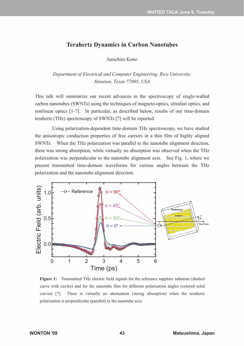
Using polarization-dependent time-domain THz spectroscopy, we have studied the anisotropic conduction properties of free carriers in a thin film of highly aligned SWNTs. When the THz polarization was parallel to the nanotube alignment direction, there was strong absorption, while virtually no absorption was observed when the THz polarization was perpendicular to the nanotube alignment axis. See Fig. 1, where we present transmitted time-domain waveforms for various angles between the THz polarization and the nanotube alignment direction.
�
�
1.0
0.5
0.0
Ele
ctric
Fie
ld (
arb.
uni
ts)
6543210Time (ps)
��= 90º
� = 45°
� = 30°
� = 0°
Reference
Reference
Figure 1: Transmitted THz electric field signals for the reference sapphire substrate (dashed
curve with circles) and for the nanotube film for different polarization angles (colored solid
curves) [7]. There is virtually no attenuation (strong absorption) when the terahertz
polarization is perpendicular (parallel) to the nanotube axis.
INVITED TALK June 9, Tuesday
WONTON '09 43 Matsushima, Japan
The sample was synthesized via chemical vapor deposition and transferred onto a sapphire substrate through a high temperature water etching process [8]. Through a proper model, the THz complex dynamic conductivity of the SWNTs was extracted and showed a non-Drude-like frequency dependence, with the real part monotonically increasing with increasing frequency. In addition, the real part of the dielectric constant showed negative values, indicating the highly metallic nature of carrier conduction along the nanotube direction. The degree of polarization in terms of absorbance was calculated to be 1, and the reduced linear dichroism was calculated to be 3 using the theory of linear dichroism for an ensemble of anisotropic molecules, which demonstrates the nematic order parameter of the SWNTs in the film to be 1. This indicates that the alignment of the nanotubes is “perfect” and any misalignment must have characteristic length scales much smaller than the wavelengths used in these experiments (1.5 mm – 150 �m). All these findings suggest that this type of aligned SWNT film performs as an ideal linear polarizer in the THz frequency range.
This work was performed in collaboration with Lei Ren, Layla G. Booshehri, William D. Rice, Xiangfeng Wang, David J. Hilton, Takashi Arikawa, Cary L. Pint, Robert H. Hauge, Aleksander K. Wojcik, Alexey A. Belyanin, Yoshiaki Takemoto, Kei Takeya, Iwao Kawayama, and Masayoshi Tonouchi.
References
1. J. Shaver et al., Nano Lett. 7, 1851 (2007); Laser & Photon. Rev. 1, 260 (2007); Phys. Rev. B 78, 081402(R) (2008).
2. A. Srivastava et al., Phys. Rev. Lett. 101, 087402 (2008). 3. J. Shaver et al., ACS Nano 3, 131 (2009). 4. J.-H. Kim et al., Phys. Rev. Lett. 102, 037402 (2009). 5. Y. Murakami and J. Kono, Phys. Rev. Lett. 102, 037401 (2009). 6. A. Srivastava and J. Kono, Phys. Rev. B 79, 205407 (2009). 7. L. Ren et al., arxiv.0903.2583v1. 8. C. L. Pint et al., ACS Nano 2, 1871 (2008).
Corresponding Author: Junichiro Kono Email: [email protected]
INVITED TALK June 9, Tuesday
WONTON '09 44 Matsushima, Japan
Exciton Fine Structures and Dynamics Studied by Single Carbon Nanotube Spectroscopy
Kazunari Matsuda
Institute for Chemical Research, Kyoto University, Uji, Kyoto 611-0011, Japan
§1 Introduction
The electronic properties of single-walled carbon nanotubes (SWNTs) have attracted
a great deal of attention because of their degenerated band structures in
momentum-space and enhanced Coulomb interaction. The enhanced Coulomb
interaction leads to the formation of excitons with large binding energies of 200–400
meV. The novel optical properties in SWNTs arise from characteristics of the excitons
[1,2]. Recently, there are several studies about optically-forbidden (dark) exciton states
in SWNTs [3,4]. The dark exciton state near the lowest optically-allowed (bright) state
has great influence on the optical properties. Here, we study the exciton fine structures
and dynamics between the bright and dark states by single nanotube spectroscopy.
§2 Experimental
The samples used in this work were suspended SWNTs synthesized on Si substrates
using an alcohol catalytic chemical vapor deposition method [5-7]. The
photoluminescence (PL) spectroscopy of a single carbon nanotube was carried out using
a variable-temperature confocal microscope. The samples were mounted in a cryostat
under a superconducting magnet with fields up to 7 T.
§3 Results and Discussion
We studied diameter and temperature dependence of PL spectra of single SWNTs.
The PL linewidth of a single carbon nanotube (homogeneous linewidth) at room
temperature depends on the diameter. Furthermore, the value of the homogeneous
linewidth almost linearly decreases with a decrease of temperature from 300 to 5 K. The
temperature dependence of the homogeneous linewidth implies that the exciton
decoherence is dominated by the diameter dependent exciton-phonon interaction [6,7].
The very narrow PL spectra of single SWNTs at low temperatures allow us to observe
small spectral changes under low magnetic fields. A single PL peak arising from the
bright exciton is observed at zero magnetic field. With increasing the magnetic field
parallel to the tube axis, we have observed another PL peak a few meV below the bright
INVITED TALK June 9, Tuesday
WONTON '09 45 Matsushima, Japan
exciton PL peak at low temperatures [8]. The additional peak arises from the dark
exciton due to the symmetry breaking caused by the Aharonov-Bohm effect. We have
also investigated temperature and magnetic field dependence of the PL intensity ratio of
the dark to bright exciton, and found that excitons are nonequilibriumly distributed
(nonBoltzmann distribution) between the bright and dark exciton states.
§4 Conclusion
We studied temperature and magnetic field dependence of PL spectra of a single
carbon nanotube. The experimental results indicate that the exciton decoherence is
dominated by the diameter dependent exciton-phonon interaction. Direct observation of
the dark exciton PL peak under magnetic field by single nanotube spectroscopy revealed
a non-equilibriumly exciton distribution between the bright and dark state.
Acknowledgement
The author thanks Mr. R. Matsunaga, Dr. Y. Miyauchi, and Prof. Y. Kanemitsu for
collaboration of the study. This study was supported by a Grant-in-Aid for Scientific
Research on Priority Area of the MEXT of Japan (Nos. 20048004, and 20340075).
References
1. H. Hirori, K. Matsuda, Y. Miyauchi, S. Maruyama, and Y. Kanemitsu, Phys. Rev. Lett.
97, 257401 (2006).
2. A. Ueda, K. Matsuda, T. Tayagaki, and Y. Kanemitsu, Appl. Phys. Lett. 92, 233105
(2008).
3. T. Ando, J. Phys. Soc. Jpn. 75, 024707 (2006).
4. J. Shaver, J. Kono, O. Portugall, V. Krstic, G. L. J. A. Rikken, Y. Miyauchi, S.
Maruyama, and V. Perebeinos, Nano Lett. 7, 1851 (2007).
5. K. Matsuda, T. Inoue, Y. Murakami, S. Maruyama, and Y. Kanemitsu, Phys. Rev. B
77, 193405 (2008).
6. K. Matsuda, T. Inoue, Y. Murakami, S. Maruyama, and Y. Kanemitsu, Phys. Rev. B
77, 033406 (2008).
7. K. Yoshikawa, R. Matsunaga, K. Matsuda, and Y. Kanemitsu, Appl. Phys. Lett. 94,
093109 (2009).
8. R. Matsunaga, K. Matsuda, and Y. Kanemitsu, Phys. Rev. Lett. 101, 147404 (2008).
Corresponding Author: Kazunari Matsuda
Email: [email protected]
INVITED TALK June 9, Tuesday
WONTON '09 46 Matsushima, Japan

WONTON '09 47 Matsushima, Japan

WONTON '09 48 Matsushima, Japan
Our Recent Advances in Nanotube and Graphene Research
Mildred Dresselhaus1, 2 and Jing Kong1
1Department of Electrical Engineering and Computer Science, Massachusetts Institute
of Technology, Cambridge, MA 02139, USA 2Department of Physics, Massachusetts Institute of Technology, Cambridge, MA 02139,
USA
A report is presented on recent advances in the Dresselhaus-Kong group at MIT on
several topics relevant to Nanotube and Graphene Photophysics research. First we
review progress with studies of the Raman spectra of individual double wall carbon
nanotubes (DWNTs), making comparisons between the work in our group and by others
doing similar measurements at the single DWNT level, making comparisons between
individual SWNTs and individual DWNTs, between individual DWNTs and bundled
DWNTs, and between CVD-derived DWNTs and peapod-derived DWNTs as bundles
and at the individual level. Recent results are reported for several features in the
Raman spectra of metallic tubes as a function of gate voltage in an electrochemical
cell, with comparisons made between experiment and theory. Results from a study of
the resonance window for members of (2n+m) families of SWNTs are reported for both
metallic and semiconducting families with a discussion of the implications of this work.
The use of Raman spectroscopy to characterize large area graphene films grown on a
(111) Nickel polycrystalline substrate is discussed with particular reference made to the
number of graphene layers. Comparisons are made with the Raman spectra obtained
by other methods of growing few layer graphene. The use of Raman spectroscopy to
study the large differences between edges in graphene ribbons when prepared by joule
heating under far from equilibrium conditions and under near equilibrium conditions is
also discussed.
Corresponding Author: Mildred Dresselhaus
Email: [email protected]
INVITED TALK June 10, Wednesday
WONTON '09 49 Matsushima, Japan
Optical properties of monolayer and bilayer graphene
Tsuneya Ando,1 Mikito Koshino,1 and Kenichi Asano2
1Department of Physics, Tokyo Institute of Technology
2–12–1 Ookayama, Meguro-ku, Tokyo 152-8551, Japan
2Department of Physics, Osaka University
1–1 Machikaneyama, Toyonaka 560-0043, Japan
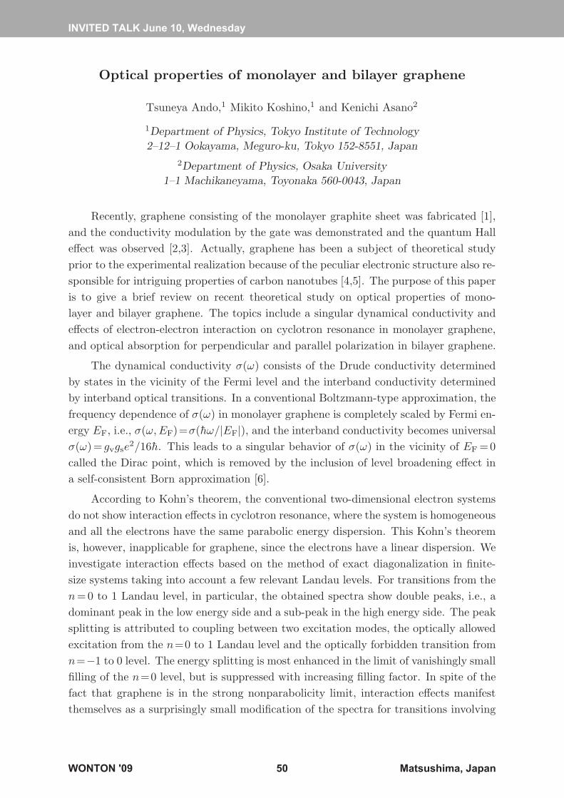
Recently, graphene consisting of the monolayer graphite sheet was fabricated [1],and the conductivity modulation by the gate was demonstrated and the quantum Halleffect was observed [2,3]. Actually, graphene has been a subject of theoretical studyprior to the experimental realization because of the peculiar electronic structure also re-sponsible for intriguing properties of carbon nanotubes [4,5]. The purpose of this paperis to give a brief review on recent theoretical study on optical properties of mono-layer and bilayer graphene. The topics include a singular dynamical conductivity andeffects of electron-electron interaction on cyclotron resonance in monolayer graphene,and optical absorption for perpendicular and parallel polarization in bilayer graphene.
The dynamical conductivity σ(ω) consists of the Drude conductivity determinedby states in the vicinity of the Fermi level and the interband conductivity determinedby interband optical transitions. In a conventional Boltzmann-type approximation, thefrequency dependence of σ(ω) in monolayer graphene is completely scaled by Fermi en-ergy EF, i.e., σ(ω, EF)=σ(h̄ω/|EF|), and the interband conductivity becomes universalσ(ω)= gvgse
2/16h̄. This leads to a singular behavior of σ(ω) in the vicinity of EF =0called the Dirac point, which is removed by the inclusion of level broadening effect ina self-consistent Born approximation [6].
According to Kohn’s theorem, the conventional two-dimensional electron systemsdo not show interaction effects in cyclotron resonance, where the system is homogeneousand all the electrons have the same parabolic energy dispersion. This Kohn’s theoremis, however, inapplicable for graphene, since the electrons have a linear dispersion. Weinvestigate interaction effects based on the method of exact diagonalization in finite-size systems taking into account a few relevant Landau levels. For transitions from then=0 to 1 Landau level, in particular, the obtained spectra show double peaks, i.e., adominant peak in the low energy side and a sub-peak in the high energy side. The peaksplitting is attributed to coupling between two excitation modes, the optically allowedexcitation from the n=0 to 1 Landau level and the optically forbidden transition fromn=−1 to 0 level. The energy splitting is most enhanced in the limit of vanishingly smallfilling of the n=0 level, but is suppressed with increasing filling factor. In spite of thefact that graphene is in the strong nonparabolicity limit, interaction effects manifestthemselves as a surprisingly small modification of the spectra for transitions involving
INVITED TALK June 10, Wednesday
WONTON '09 50 Matsushima, Japan
0 1 2 30
5
10
15
20
25
30
35
Frequency (units of Δ/h)
Dyn
amic
al C
ondu
ctiv
ity (
units
of σ
0)
eFextd/Δ= 0.00δ/Δ=0.02Δ=0.40 (eV)κ=2.00
Re ~σ(ω) Re σ(ω)
0.00 0.00
0.25 0.15
0.50 0.29
0.75 0.40
1.00 0.49
1.25 0.57
1.50 0.65
ns/ns0 eFd/Δ
0 1 2 30
5
10
15
20
Frequency (units of Δ/h)
Dyn
amic
al C
ondu
ctiv
ity (
units
of g
vgse
2 /2π
h) eFextd/Δ= 0.00δ/Δ=0.02κ=2.0
0.00 0.00
0.25 0.15
0.50 0.29
0.75 0.40
1.00 0.49
1.25 0.57
1.50 0.65
ns/ns0 eFd/Δ
Fig. 1 Absorption for perpendicular (left) and parallel polarization (right).
level n=0 in the presence of broadening. This situation changes for other transitionssuch as those from n=−1 to n=2.
Graphene bilayer has a unique band structure distinct from monolayer graphene,where the conduction and valence bands with quadratic dispersion touch at zero Fermienergy [7,8]. An important property is that an electric-field applied perpendicularly tothe layers modifies its low-energy band structure by opening an energy gap between theelectron and hole bands [9,10]. Another interesting feature is that optical transitionscan be induced by light polarized both parallel and perpendicular to the layer.
For the perpendicular polarization, in particular, the effective dynamical conduc-tivity giving the absorption is calculated with inclusion of the depolarization effectassociated with induced charge redistribution between two layers. Spectral features,characterized by peaks and edges associated with specific transitions between sub-bands, are quite different between perpendicular and parallel polarizations, becauseeach of transitions can be allowed or prohibited depending on the polarization direc-tion. For the perpendicular light, the absorption energy is considerably shifted by thedynamical screening effect, while that is absent for parallel polarization.
References[1] K. S. Novoselov, A. K. Geim, S. V. Morozov, D. Jiang, Y. Zhang, S. V. Dubonos,
I. V. Grigorieva, and A. A. Firsov, Science 306 (2004) 666.[2] K. S. Novoselov, A. K. Geim, S. V. Morozov, D. Jiang, M. I. Katsnelson, I. V.
Grigorieva, S. V. Dubonos, and A. A. Firsov, Nature 438 (2005) 197.[3] Y. Zhang, Y.-W. Tan, H. L. Stormer, and P. Kim, Nature 438 (2005) 201.[4] T. Ando, J. Phys. Soc. Jpn. 74 (2005) 777.[5] T. Ando, Physica E 40 (2007) 213 and references cited therein.[6] T. Ando, Y. Zheng, and H. Suzuura, J. Phys. Soc. Jpn. 71 (2002) 1318.[7] E. McCann and V. I. Falko, Phys. Rev. Lett. 96 (2006) 086805.[8] M. Koshino and T. Ando, Phys. Rev. B 73 (2006) 245403.[9] E. McCann, Phys. Rev. B 74 (2006) 161403.
[10] T. Ando and M. Koshino, J. Phys. Soc. Jpn. 78 (2009) 034709.
INVITED TALK June 10, Wednesday
WONTON '09 51 Matsushima, Japan
Raman, Photoluminescence and Saturable Absorption in Graphene
Andrea C. Ferrari Engineering Department, Cambridge University, Cambridge, UK
I will review some recent advances in optoelectronic and photonics of graphene layers. Raman spectroscopy is one of the most powerful tools for graphene characterisation [1] I will first focus on the effects of uniaxial strain on its Raman spectrum [2]. The doubly degenerate E2g optical mode splits in two components, one polarized along the strain and the other perpendicular to it. This leads to the splitting of the G peak into two bands, which we call G+ and G-, by analogy with the effect of curvature on the nanotube G peak. Their relative intensities depend on light polarization, which allows one to determine the graphene crystallographic orientation with respect to the applied strain [2]. I will then discuss the dependence of the 2D peak intensity on doping [4-6] and show that this is determined by a combination of electron-phonon and electron-electron scattering [6]. Under full resonance, the generated electron-hole pairs can scatter not just with phonons, but also with electrons and holes, and this affects the 2D peak intensity [6]. This explains quantitatively the experimental doping dependence of the 2D peak and can be used to determine its Electron Phonon Coupling, which is higher than previously predicted by density-functional theory, as a consequence of the renormalization by Coulomb interactions [6]. Finally I will discuss how to induce significant photoluminescence in graphene [8], and how to exploit Pauli blocking to realise an ultrafast laser based on graphene as saturable absorber [9]. The latter examples show the viability of graphene for optoelectronics.
1. A. C. Ferrari et al. Phys. Rev. Lett. 97, 187401 (2006) 2. T. M. G. Mohiuddin et al. arXiv:0812.1538 (2008) 4. S. Pisana et al. Nature Mater. 6, 198 (2007) 5. A. Das et al, Nature Nano 3, 210 (2008). 6. C. Casiraghi et al. Appl. Phys Lett. 91, 233108 (2007) 7. D. M. Basko, S. Piscanec, A. C. Ferrari, submitted (2009) 8. R.R. Nair, T. Gokus, M. Bohmler, A. Lombardo, A. Bonetti, K. S. Novoselov, A K. Geim, A. Hartschuh, A. C. Ferrari, submitted (2009) 9. Z. Sun, T. Hasan, F. Torrisi, D. Popa, F. Bonaccorso, A. C. Ferrari, submitted (2009)
INVITED TALK June 10, Wednesday
WONTON '09 52 Matsushima, Japan
Electronic and Optical Properties of Nanotubes, Graphene, and Graphene Nanostructures
Steven G. Louie
Department of Physics, University of California, Berkeley, California 94720, USA Materials Sciences Division, Lawrence Berkeley National Laboratory, Berkeley, California 94720, USA
Fax: +1-510-643-9473 E-mail address: [email protected]
The low-energy electronic states in graphene behave like those of two-dimensional (2D) massless Dirac fermions with pseudospin character. Many of the unusual electronic, transport and optical properties of carbon nanotubes and graphene and graphene-based nanostructures originate from this unique electronic structure. Abinitio calculations further showed that, because of reduced dimensionality, electron-electron interaction effects are very important in the quasiparticle and optical excitations in these systems. In this talk, we illustrate these effects with results from several recent theoretical studies. Single-walled carbon nanotubes (SWCNTs) exhibit highly unusual exciton excited-state spectra owing to a 1D anti-screening effect. First-principles calculations on excitonic effects in the nonlinear optical properties of SWCNTs will also be presented. For graphene-based nanostructures, we show that they possess further fascinating properties. Graphene nanoribbons are semiconductors with novel electronic, magnetic and optical properties. For example, the existence of magnetic edge-state excitons is predicted for zigzag-edged nanoribbons. Owing to the chiral nature of the electronic states, the carrier dynamics in graphene exhibits anomalous anisotropy when subjected to an external periodic potential of nanometer dimensions (called graphene superlattices). Under appropriate conditions, these graphene superlattices are predicted to be electron supercollimators and new generation of 2D massless Dirac fermions may be created.
INVITED TALK June 10, Wednesday
WONTON '09 53 Matsushima, Japan
Effects of Environment and Defects on Photoluminescence of Single Wall Carbon Nanotube
Yoshikazu Homma, Shohei Chiashi, Ryota Mitobe, and Kotaro Nagatsu
Department of Physics, Tokyo University of Science
1-3 Kagurazaka, Shinjuku-ku, Tokyo 162-8601, Japan
§1 Introduction
Single wall carbon nanotubes (SWNTs) are promising materials for
nano-electronics applications. In addition to peculiar electric properties originated from
one dimensionality of SWNTs, semiconducting SWNTs exhibit intense
photoluminescence (PL) owing to a direct bandgap and high densities of singular
electronic states. However, since all the carbon atoms are in the surface layer, PL of
SWNTs suffers from strong influence by the surrounding materials. They become
unluminescent when lying on a substrate. Investigation into the effect of adsorbates is
thus important for elucidating the PL quenching mechanism. Defects on the wall should
also affect the PL properties. We have studied the effects of adsorbates and defects using
individual SWNTs suspended between micropillars.
§2 Investigation of Adsorbate Effect
We have used an environmental chamber to control the gas (ethanol or water
vapor) ambience surrounding suspended SWNTs. Both PL excitation and emission
energies of a suspended SWNT rapidly change at a transition pressure [1]. The
transition pressure shows clear diameter dependence: the transition pressure decreases
with an increase in the tube diameter. This phenomenon is quantitatively described by
adsorption and desorption of molecules on the SWNT surface. Condensation of gas
molecules on the SWNT surface causes change in the dielectric constant, which affects
the binding energy of exciton.
Deposition of carbon, on the other hand, causes formation of satellite peaks only
in the emission spectrum. The excitation energy remains the same after carbon
deposition, while the emission intensity decreases with increasing the amount of carbon
deposited. The carbon deposits on the SWNT wall induce new electronic levels.
Deposition of non-wetting metals, such as gold and iron, on a SWNT shows a
different effect on PL. Metal deposits induce tensile strain on the nanotube, thus the
emission energy shifts depending on the family-type of nanotube.
INVITED TALK June 10, Wednesday
WONTON '09 54 Matsushima, Japan
§3 Investigation of Defect Effect
We are now studying the effect of defect creation by irradiating a SWNT with an
electron beam in a scanning electron microscope (SEM). SEM observation is known to
cause sizable damage in SWNTs [2]. However, it was difficult to distinguish between
the defect creation and contamination deposition effects. Thus, we use electron
irradiation at elevated temperatures, which can reduce contamination deposition during
SEM observation.
For the investigation of defect effects, observation of PL in a microscopic scale is
useful. Thus, we are developing a high-spatial resolution PL system using a near-filed
scanning optical microscope (NSOM) combined with the laser-excited PL system.
Suspended SWNTs formed on narrow-gap grooves can be imaged with the scanning
probe. We expect spatial resolution on the order of 10 nm.
Acknowledgement
This work was supported by Grant-in-Aid for Scientific Research on Priority Area of
the Ministry of Education, Culture, Sports, Science and Technology of Japan (MEXT).
References
1. S. Chiashi, S. Watanabe, T. Hanashima and Y. Homma, Nano Lett. 8 3097 (2008)
2. S. Suzuki, K. Kanzaki, Y. Homma and S. Fukaba, Jpn. J. Appl. Phys. Part 2 43 L118
(2004).
Corresponding Author: Y. Homma
Email: [email protected]
INVITED TALK June 10, Wednesday
WONTON '09 55 Matsushima, Japan
Quantum optics with carbon nanotubes
C. Galland, A. Hoegele, and A. Imamoglu
Institute of Quantum Electronics, ETH Zurich, 8093 Zurich, Switzerland
Semiconducting carbon nanotubes (CNT) constitute a new paradigm for solid-state
quantum optics. I will discuss recent experiments where we have used photon
correlation measurements to demonstrate that unintentional exciton localization could
lead to strong photon antibunching in a single CNT [1]. Our experiments also
demonstrated that the confined exciton photoluminescence (PL) lineshape could be
highly asymmetric [2]. The independent boson model that we use to describe the
confined exciton-phonon interactions reproduce with very high accuracy the broad and
asymmetric PL lines observed in these experiments. A principal goal of future
experiments is the demonstration of all-optical spin manipulation in CNTs [3].
References
1. A. Hoegele, G. Galland, M. Winger, and A. Imamoglu, Phys. Rev. Lett. 100, 217401
(2008).
2. C. Galland, A. Hoegele, H. Tureci, and A. Imamoglu, Phys. Rev. Lett. 101, 067402
(2008).
3. C. Galland and A. Imamoglu, Phys. Rev. Lett. 101, 157404 (2008).
Corresponding Author: Atac Imamoglu
Email: [email protected]
INVITED TALK June 10, Wednesday
WONTON '09 56 Matsushima, Japan
Third-Order Nonlinear Optical Response in Fullerene-Peapods
A. Nakamura1, D. Hosooka1, T. Koyama1, H. Kishida1, K. Asaka1, Y. Saito1,
and T. Saito2
1Department of Applied Physics, Nagoya University
Furo-cho, Chikusaku, Nagoya 464-8603 Japan 2 Research Center for Advanced Carbon Materials, AIST,
1-1-1 Higashi, Tsukuba, 305-8565, Japan
§1 Introduction
It is known that quasi-one-dimensional exciton effects near the fundamental
absorption edge in single-walled carbon nanotubes (SWNTs) enhance optical
nonlinearities in the near-infrared region[1,2]. Fullerene-peapods are also of interest to
investigate optical properties because of the unique structure consisting of one- and
zero-dimensional systems. The theoretical study has predicted significant modification
of electronic states in peapods due to hybridization between � states of fullerenes and
nearly free electron states of SWNTs [3]. In this presentation, we report on third-order
nonlinear optical susceptibilities in carbon peapods encapsulating C60, C70 and C84
studied by femtosecond pump-probe spectroscopy.
§2 Experiments
SWNTs with the average diameter of 1.9 ± 0.4 nm were produced by the direct
injection pyrolytic synthesis method using colloidal solutions of metal nanoparticles
containing Co and Mo. Peapods were made by heating a quartz ampoule containing a
dry mixture of C60 (C70 or C84) and SWNT at 650 C. After the heat treatment the
mixture was washed with toluene to remove any excess fullerene molecules from the
outside of the SWNTs. For comparison of optical properties of the fullerene-peapods
with those of SWNTs, we also prepared SWNT samples without containing fullerenes
with the same procedures. Pump-probe measurements were carried out using a 120
fs-width pump pulse with the photon energy of 2.5�3.1 eV and a white continuum probe
pulse.
§3 Results and discussion
Figure 1(a) shows the absorption spectra of C84-peapods (solid curve) and
reference-SWNTs (dashed curve). Two absorption bands due to the E22 excitonic
transition (~0.9 eV) of semiconductor tubes and the M11 transition (~1.3 eV) of metal
INVITED TALK June 10, Wednesday
WONTON '09 57 Matsushima, Japan
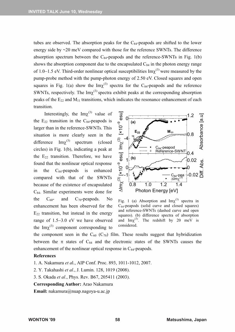
tubes are observed. The absorption peaks for the C84-peapods are shifted to the lower
energy side by ~20 meV compared with those for the reference SWNTs. The difference
absorption spectrum between the C84-peapods and the reference-SWNTs in Fig. 1(b)
shows the absorption component due to the encapsulated C84 in the photon energy range
of 1.0�1.5 eV. Third-order nonlinear optical susceptibilities Im(3) were measured by the
pump-probe method with the pump-photon energy of 2.50 eV. Closed squares and open
squares in Fig. 1(a) show the Im(3) spectra for the C84-peapods and the reference
SWNTs, respectively. The Im(3) spectra exhibit peaks at the corresponding absorption
peaks of the E22 and M11 transitions, which indicates the resonance enhancement of each
transition.
Interestingly, the Im(3) value of
the E22 transition in the C84-peapods is
larger than in the reference-SWNTs. This
situation is more clearly seen in the
difference Im(3) spectrum (closed
circles) in Fig. 1(b), indicating a peak at
the E22 transition. Therefore, we have
found that the nonlinear optical response
in the C84-peapods is enhanced
compared with that of the SWNTs
because of the existence of encapsulated
C84. Similar experiments were done for
the C60- and C70-peapods. No
enhancement has been observed for the
E22 transition, but instead in the energy
range of 1.5�3.0 eV we have observed
the Im(3) component corresponding to
the component seen in the C60 (C70) film. These results suggest that hybridization
between the � states of C84 and the electronic states of the SWNTs causes the
enhancement of the nonlinear optical response in C84-peapods.
-4
0
0.4
0.8
1.2
Photon Energy [eV]
Im
References
1. A. Nakamura et al., AIP Conf. Proc. 893, 1011-1012, 2007.
2. Y. Takahashi et al., J. Lumin. 128, 1019 (2008).
3. S. Okada et al., Phys. Rev. B67, 205411 (2003).
Corresponding Author: Arao Nakamura
Email: [email protected]
Fig. 1 (a) Absorption and Im(3) spectra in C84-peapods (solid curve and closed squares) and reference-SWNTs (dashed curve and open squares). (b) difference spectra of absorption and Im(3). The redshift by 20 meV is considered.
(3) [
×10
–9 e
su]
Abs
orba
nce
[a.u
]
C84-peapod Reference-SWNT
E22 M11
0.8 1.0 1.2 1.4
-1
0
1
-0.02
0
0.02
Diff
. Abs
.
Im
[×–9
esu
](3
)10
C84-peaIm(3)
(a)
(b)
INVITED TALK June 10, Wednesday
WONTON '09 58 Matsushima, Japan
Direct Determination of Precise Electronic States of SWNTs Based on Soluble Carbon Nanotubes
Naotoshi Nakashima
Department of Applied Chemistry, Graduate School of Engineering, Kyushu University, Fukuoka 819-0395 Japan
Japan Science and Technology Agency, CREST
Since the discovery of carbon nanotubes (CNTs), many groups have endeavored
to understand the fundamental properties of the CNTs and explored their applications in
nanomaterials science and engineering. Electronic structures of CNTs, one of the most
fundamental features of nanotubes, strongly depend on the chirality of the nanotubes.
We have discovered that we can determine the precise electronic states of isolated
SWNTs having their own chirality indices by in situ near-IR photoluminescence
spectroelectrochemistry at the fabricated modified ITO electrode. This has been
achieved by using this modifying film that retains the isolated SWNTs and the
spectroelectrochemical results analyzed by Nernst equation. Table1 summarized the
results of fifteen individual SWNTs having chirality indices of (6,5), (8,3), (7,5), (8,4),
(10,2), (7,6), (9,4), (10,3), (8,6), (9,5), (12,1), (11,3), (8,7), (10,5), and (9,7).
Details including direct determination of precise electronic states of SWNTs, as
well as fundamental and applications of “soluble carbon nanotubes” 1 will be reported at
the meeting.
References
1. (a) N. Nakashima, T. Fujigaya, “Soluble carbon nanotubes and nanocomposite materials”,
Encyclopedia of Nanoscience and Nanotechnology”, in press; (b) N. Nakashima, A. Fujigaya,
H. Murakami, “Soluble Carbon Nanotubes”, in Chemistry of Carbon Nanotubes, eds, V. A.
Basiuk, and E. V. Basiuk, American Scientific Publisher, California, 2008, pp.113-128
(Chapter 6); (c) T. Fujigaya, N. Nakashima, “Methodology for Homogeneous Dispersion of
Single-walled Carbon Nanotubes by Physical Modification”, Poly. J. (Review article), 40,
577-589 (2008); (d) N. Nakashima, A. Fujigaya, “Fundamental and Applications of Soluble
Carbon Nanotubes”, Chem. Lett. (Highlight Review), 36, 692-697 (2007); (e) N. Nakashima,
“Solubilization of Single-Walled Carbon Nanotubes with Condensed Aromatic Compounds”,
Sci. & Tech. Adv. Mater., 7, 609-616 (2006); (f) H. Murakami, N. Nakashima, “Soluble
Carbon Nanotubes and Their Applications”, J. Nanosci. Nanotechnol., 6, 16-27 (2006); (g)
INVITED TALK June 10, Wednesday
WONTON '09 59 Matsushima, Japan
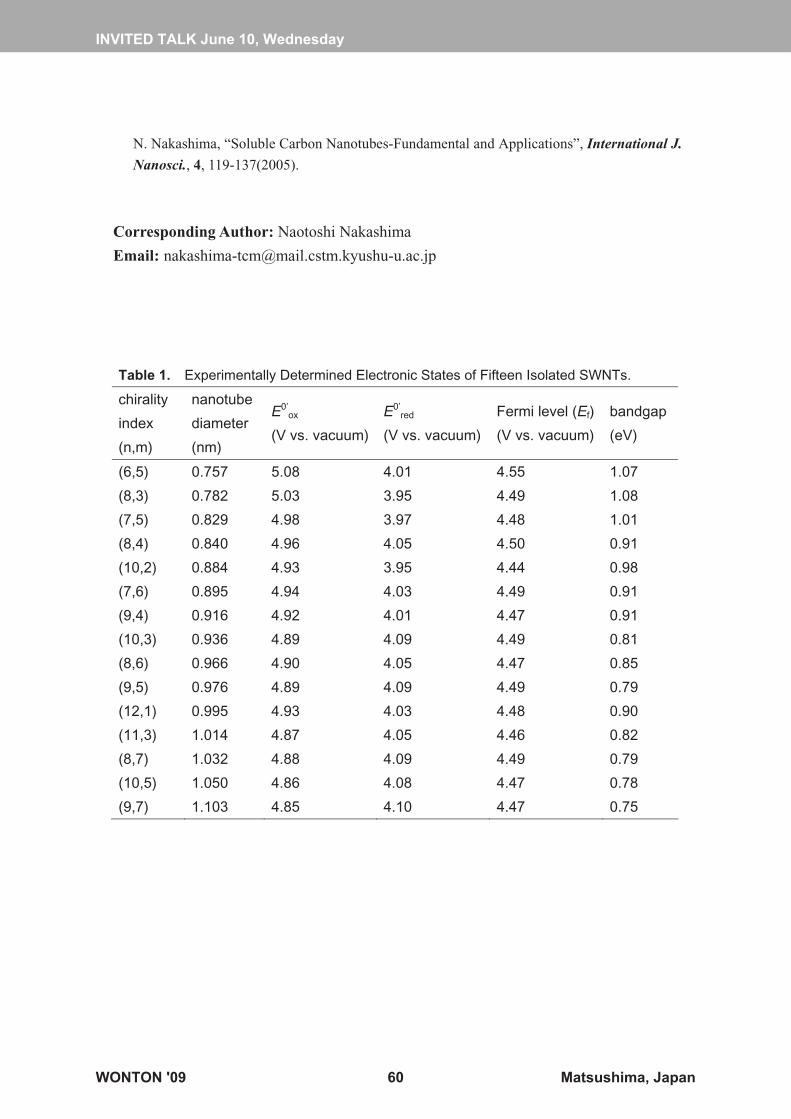
N. Nakashima, “Soluble Carbon Nanotubes-Fundamental and Applications”, International J.
Nanosci., 4, 119-137(2005).
Corresponding Author: Naotoshi Nakashima
Email: [email protected]�
Table 1. Experimentally Determined Electronic States of Fifteen Isolated SWNTs.
chirality
index
(n,m)
nanotube
diameter
(nm)
E0’ox
(V vs. vacuum)
E0’red
(V vs. vacuum)
Fermi level (Ef)
(V vs. vacuum)
bandgap
(eV)
(6,5) 0.757 5.08 4.01 4.55 1.07
(8,3) 0.782 5.03 3.95 4.49 1.08
(7,5) 0.829 4.98 3.97 4.48 1.01
(8,4) 0.840 4.96 4.05 4.50 0.91
(10,2) 0.884 4.93 3.95 4.44 0.98
(7,6) 0.895 4.94 4.03 4.49 0.91
(9,4) 0.916 4.92 4.01 4.47 0.91
(10,3) 0.936 4.89 4.09 4.49 0.81
(8,6) 0.966 4.90 4.05 4.47 0.85
(9,5) 0.976 4.89 4.09 4.49 0.79
(12,1) 0.995 4.93 4.03 4.48 0.90
(11,3) 1.014 4.87 4.05 4.46 0.82
(8,7) 1.032 4.88 4.09 4.49 0.79
(10,5) 1.050 4.86 4.08 4.47 0.78
(9,7) 1.103 4.85 4.10 4.47 0.75
INVITED TALK June 10, Wednesday
WONTON '09 60 Matsushima, Japan
Electronic and Geometrical Properties of Carbon Nanotubes: A First-Principles Study
Susumu Saito
Department of Physics, Tokyo Institute of Technology 2-12-1 Oh-okayama, Meguro-ku, Tokyo 152-8551, Japan
§1 Introduction
Electronic properties of carbon nanotubes (CNTs) have been studied intensively
so far. One of their most important electronic properties, the topology-dependent
metallic versus semiconducting transport properties, were predicted theoretically based
on the tight-binding approximation [1,2]. From the viewpoint of the next-generation
nanoelectronics materials, so-called armchair nanotubes are of high interest as metallic
nanowires to be used in the nanometer-scale devices, partly due to the high maximum
electric current density they can host, and partly due to their high thermal conductivity
because the appropriate heat treatment is the key to miniaturizing the electronics devices
further and furthre in the future. On the other hand, carbon nanotubes which are either
moderate-gap or narrow-gap semiconductors can be even more important than metallic
armchair nanotubes as materials to be used to construct central functional part of the
next-generation nanodevices [3]. Therefore, predicting the precise electronic structure
of each individual carbon nanotube is highly important at present.
In addition to the study of pristine carbon nanotubes, studying the effect of doping
into semiconductor nanotubes are equally very important since, as in the case of bulk
materials, doping should be the key technology to be used in realizing both n-type and
p-type semiconductor units with nanometer scale. We have addressed these important
issues using a variety of predictive theoretical methods including the local density
approximation (LDA) in the framework of the density-functional theory, the
transferable tight-binding models which can reproduce either LDA energetics or LDA
electronic properties, and the Green-function based GW approximation [4]. Also the
production of new nanometer-scale carbon materials using carbon nanotubes by
utilizing external pressure and/or thermal effect have been theoretically studied in detail.
§2 Workfunction of metallic nanotubes
In the case of C60, it has been shown that the geometry optimization is of essential importance to predict its electronic structure [4]. The simple assumption of its
INVITED TALK June 10, Wednesday
WONTON '09 61 Matsushima, Japan
interatomic distances of graphite value is found to give as much as 0.3 eV smaller gap between the highest-occupied state and the lowest-unoccupied state than that of C60 with complete geometry optimization. Therefore, at least in the case of thin carbon nanotubes with diameters similar to or smaller than that of C60 (about 7 Å), the geometry optimization should be important as well to predict their electronic properties. We have optimized systematically the geometry of armchair nanotubes, and actually its effect is confirmed to be important to predict, for example, their workfunction values [5].
§3 Doping into semiconductor nanotubes
In the previous work, we studied the energetics and the positions of the
impurity-induced states in substitutionally B-doped carbon nanotubes [6]. The N-doped
carbon nanotubes should be equally important and we have studied them comparatively
with previous B-doped case using the LDA. Interesting differences between B and N
doped cases including the exceptionally shallow N-induced impurity state in the case of
thin nanotubes is revealed.
§4 New nanocarbon phases
An atomistic process of the carbon-nanotube formation from C60 fullerenes
inside the outer nanotube via thermal treatment is simulated using the variable-cell
molecular dynamics [7]. Also the formation of various new phases from various
crystalline nanotube samples under external pressure is studied in detail [8].
Acknowledgements
The work was partly supported by Grant-in-Aid for Scientific Research on Priority Area
of the MEXT, Japan, and by the Global Center of Excellence project “Nanoscience and
Quantum Physics” of the Tokyo Institute of Technology.
References
1. N. Hamada, S. Sawada and A. Oshiyama, Phys. Rev. Lett., 68, 1579 (1992).
2. R. Saito, M. Fujita, G. Dresselhaus, and M. S. Dresselhaus, Appl. Phys. Lett. 60, 2204 (1992).
3. S. Saito, Science 278, 77 (1997).
4. S. Saito and A. Zettl, “Carbon Nanotubes: Quantum Cylinders of Graphene” (Elsevier, 2008).
5. K. Kato and S. Saito, to be published.
6. T. Koretsune and S. Saito., Phys. Rev. B 77, 165417 (2008).
7. Y. Yamagami and S. Saito, to be published.
8. M. Sakurai and S. Saito, to be published.
Email: [email protected]
INVITED TALK June 10, Wednesday
WONTON '09 62 Matsushima, Japan
Production of (5,4) and (6,4) Enriched Single-Walled Carbon Nanotubes Grown Using a Platinum Catalyst
Naoko Takamizu1,Keisuke Urata1,Toshiya Okazaki2,and Yohji Achiba1
1Department of Chemistry, Tokyo Metropolitan University, Tokyo 192-0397,Japan 2Nanotube Research Center, AIST, Tsukuba305-8568, Japan
§1 Introduction
Since the electronic and optical properties of single-wall carbon nanotubes
(SWNTs) very much depend on the tube structure1), one of the most important issues of
SWNTs is to control the distribution of nanotube diameters and chiralities in the product.
For methods in which nanotubes are grown from gaseous precursors on metallic catalyst
particles, the selection of metal catalyst is of particular importance, because the product
compositions are strongly influenced by the kinds of metallic nanoparticle materials.
For example, the CoMoCAT catalyst system has been know to give rise to thin and
narrow diameter distribution2), but HiPco, very broad abundance profile. Here, in the
present work, we will demonstrate the production of the SWNTs with narrow and very
small diameter distribution in comparison with the CoMoCAT system by use of
platinum particle as a catalyst and will show the presence of the (4,2) tube with 0.47 nm
in diameter as the smallest diameter carbon nanotube.
§2 Experimetal
The SWNT sample was synthesized by alcohol CVD method using ethanol as
carbon precursor, and platinum was used as a catalyst deposited on PG (porous glass
with average pour size of 20-30nm3)). The furnace temperature and an inner pressure of
ethanol were systematically changed with the aim of synthesizing the smaller and the
narrower diameter distributions of SWNTs. The obtained as-grown SWNTsample was
acharacterized by TEM, Raman scattering spectroscopy, and absorption and
fluorescence measurements were carried out for the sample after the conventional
dispersion and isolation procedures of the SWNTs in SDBS/water solution.
§3 Results and Discussion
It is well known that the furnace temperature, carbon source materials, and the
kind of catalyst are important parameters for controlling the compositions of the grown
SWNTs. For the purpose of production of SWNTs with the diameter distribution as
INVITED TALK June 10, Wednesday
WONTON '09 63 Matsushima, Japan
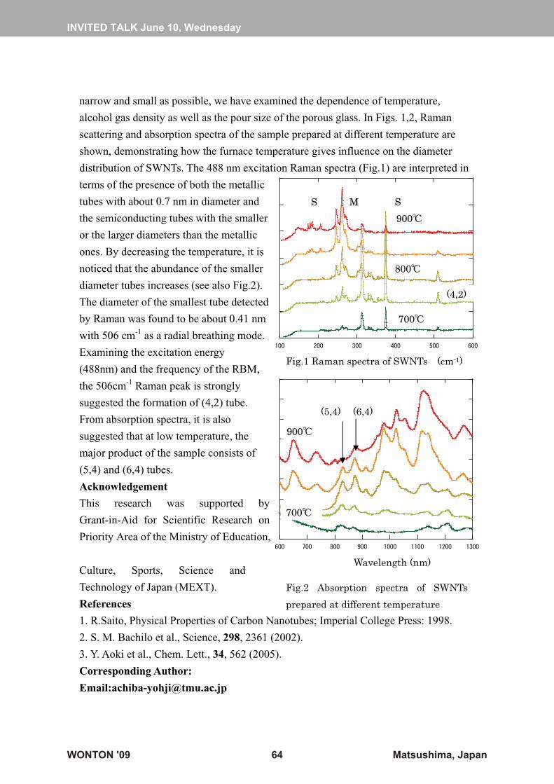
Wavelength (nm)
Fig.2 Absorption spectra of SWNTs prepared at different temperature
Fig.1 Raman spectra of SWNTs (cm-1)
narrow and small as possible, we have examined the dependence of temperature,
alcohol gas density as well as the pour size of the porous glass. In Figs. 1,2, Raman
scattering and absorption spectra of the sample prepared at different temperature are
shown, demonstrating how the furnace temperature gives influence on the diameter
distribution of SWNTs. The 488 nm excitation Raman spectra (Fig.1) are interpreted in
terms of the presence of both the metallic
tubes with about 0.7 nm in diameter and
the semiconducting tubes with the smaller
or the larger diameters than the metallic
ones. By decreasing the temperature, it is
noticed that the abundance of the smaller
diameter tubes increases (see also Fig.2).
The diameter of the smallest tube detected
by Raman was found to be about 0.41 nm
with 506 cm-1 as a radial breathing mode.
Examining the excitation energy
(488nm) and the frequency of the RBM,
the 506cm-1 Raman peak is strongly
suggested the formation of (4,2) tube.
From absorption spectra, it is also
suggested that at low temperature, the
major product of the sample consists of
(5,4) and (6,4) tubes.
S M900S
800
(4,2)
700
900
(6,4)(5,4)
Acknowledgement
This research was supported by
Grant-in-Aid for Scientific Research on
Priority Area of the Ministry of Education,
Culture, Sports, Science and
Technology of Japan (MEXT).
700
References
1. R.Saito, Physical Properties of Carbon Nanotubes; Imperial College Press: 1998.
2. S. M. Bachilo et al., Science, 298, 2361 (2002).
3. Y. Aoki et al., Chem. Lett., 34, 562 (2005).
Corresponding Author:
Email:[email protected]
INVITED TALK June 10, Wednesday
WONTON '09 64 Matsushima, Japan
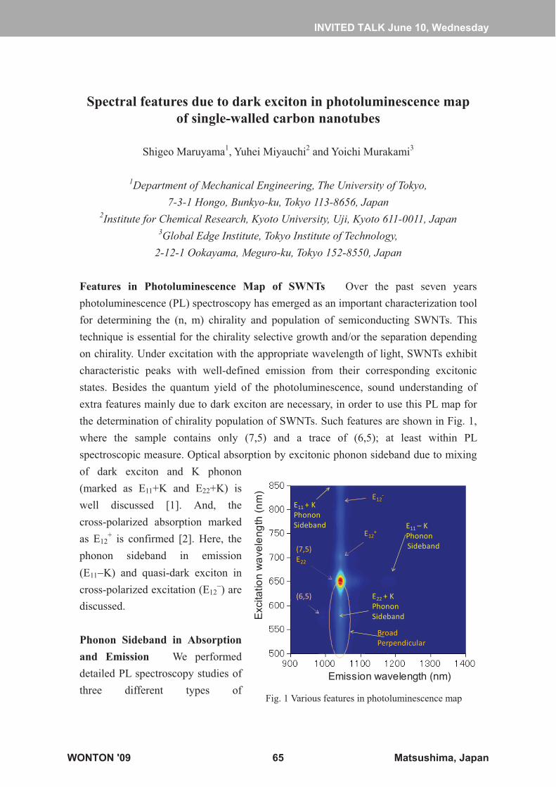
Spectral features due to dark exciton in photoluminescence map of single-walled carbon nanotubes
Shigeo Maruyama1, Yuhei Miyauchi2 and Yoichi Murakami3
1Department of Mechanical Engineering, The University of Tokyo,
7-3-1 Hongo, Bunkyo-ku, Tokyo 113-8656, Japan 2Institute for Chemical Research, Kyoto University, Uji, Kyoto 611-0011, Japan
3Global Edge Institute, Tokyo Institute of Technology, 2-12-1 Ookayama, Meguro-ku, Tokyo 152-8550, Japan
Features in Photoluminescence Map of SWNTs� Over the past seven years photoluminescence (PL) spectroscopy has emerged as an important characterization tool for determining the (n, m) chirality and population of semiconducting SWNTs. This technique is essential for the chirality selective growth and/or the separation depending on chirality. Under excitation with the appropriate wavelength of light, SWNTs exhibit characteristic peaks with well-defined emission from their corresponding excitonic states. Besides the quantum yield of the photoluminescence, sound understanding of extra features mainly due to dark exciton are necessary, in order to use this PL map for the determination of chirality population of SWNTs. Such features are shown in Fig. 1, where the sample contains only (7,5) and a trace of (6,5); at least within PL spectroscopic measure. Optical absorption by excitonic phonon sideband due to mixing of dark exciton and K phonon (marked as E11+K and E22+K) is well discussed [1]. And, the cross-polarized absorption marked as E12
+ is confirmed [2]. Here, the phonon sideband in emission (E11�K) and quasi-dark exciton in cross-polarized excitation (E12
�) are discussed. Phonon Sideband in Absorption and Emission � We performed detailed PL spectroscopy studies of three different types of
(7,5)E22
(6,5)
E11 – KPhononSideband
E22 +�KPhonon�Sideband
E11 +�KPhonon�Sideband
E12+
E12�
Broad�Perpendicular
Emission wavelength (nm)
Exc
itatio
n w
avel
engt
h (n
m)
Fig. 1 Various features in photoluminescence map
INVITED TALK June 10, Wednesday
WONTON '09 65 Matsushima, Japan
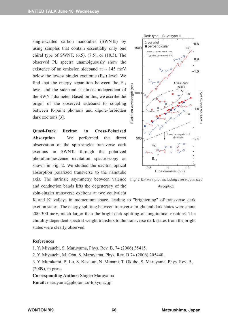
single-walled carbon nanotubes (SWNTs) by using samples that contain essentially only one chiral type of SWNT, (6,5), (7,5), or (10,5). The observed PL spectra unambiguously show the existence of an emission sideband at ~ 145 meV below the lowest singlet excitonic (E11) level. We find that the energy separation between the E11 level and the sideband is almost independent of the SWNT diameter. Based on this, we ascribe the origin of the observed sideband to coupling between K-point phonons and dipole-forbidden dark excitons [3]. Quasi-Dark Exciton in Cross-Polarized Absorption � We performed the direct observation of the spin-singlet transverse dark excitons in SWNTs through the polarized photoluminescence excitation spectroscopy as shown in Fig. 2. We studied the exciton optical absorption polarized transverse to the nanotube axis. The intrinsic asymmetry between valence and conduction bands lifts the degeneracy of the spin-singlet transverse excitons at two equivalent K and K' valleys in momentum space, leading to "brightening" of transverse dark exciton states. The energy splitting between transverse bright and dark states were about 200-300 meV, much larger than the bright-dark splitting of longitudinal excitons. The chirality-dependent spectral weight transfers to the transverse dark states from the bright states were clearly observed. References 1. Y. Miyauchi, S. Maruyama, Phys. Rev. B, 74 (2006) 35415. 2. Y. Miyauchi, M. Oba, S. Maruyama, Phys. Rev. B 74 (2006) 205440. 3. Y. Murakami, B. Lu, S. Kazaoui, N. Minami, T. Okubo, S. Maruyama, Phys. Rev. B, (2009), in press. Corresponding Author: Shigeo Maruyama Email: [email protected]
0.8 1 1.2
500
1000
1500
6
1.5
Tube diameter (nm)
Exc
itatio
n en
ergy
(eV)
parallelperpendicular
E22
E11
E12
Red: type I Blue: type II
E33
E44
Exc
itatio
n w
avel
engt
h (n
m)
2.5
1.0
0.8
0.9
Quasi-dark peaks
Broad cross-polarized absorption
Type I: 2n+m mod 3 =1Type II: 2n+m mod 3 =2
Fig. 2 Kataura plot including cross-polarized
absorption.
INVITED TALK June 10, Wednesday
WONTON '09 66 Matsushima, Japan

Abstracts
Poster Session
WONTON '09 67 Matsushima, Japan

WONTON '09 68 Matsushima, Japan
Enrichment of Armchair Carbon Nanotubes via Density Gradient Ultracentrifugation: Raman Spectroscopy Evidence
Erik H. Hároz1, William D. Rice1, Benjamin Y. Lu1, Robert H. Hauge2, Saunab Ghosh2, R. Bruce Weisman2, Pavel Nikolaev3, Sivaram Arepalli3, Donny Magana4, Stephen K. Doorn4, and Junichiro Kono1
1Department of Electrical & Computer Engineering, Rice University, MS-366, Houston,
Texas 77005, USA 2Department of Chemistry, Rice University, MS-60, Houston, Texas 77005, USA
3Johnson Space Center, National Aeronautics & Space Administration, Houston, Texas 77058, USA
4Division of Chemistry, Los Alamos National Laboratory, Mailstop J563, Los Alamos, New Mexico 87545, USA
We have performed resonant Raman scattering studies of single-walled carbon nanotubes (SWNTs), enriched in metallic (n,m) species [or (n�m) mod 3 = 0] by the density gradient ultracentrifugation (DGU) technique. Through these studies, we provide evidence for a strong enrichment in armchair and near-armchair (n,m)
species not previously observed optically. These measurements were carried out over a broad range of excitation wavelengths (440-850 nm) such that all (n,m) species remaining in the enriched material were identified. When compared to pristine, as-produced SWNT material, Raman results indicate the almost complete suppression of semiconducting [or (n�m) mod 3 = ±1] SWNTs, confirming observations by absorption and photoluminescence excitation spectroscopy. Additionally, clear Raman excitation profiles (REPs) of the radial breathing mode (RBM) were generated for all armchair (n,n) nanotubes from (6,6) through (12,12). A comparison between the REPs of armchair SWNTs and the other metallic species over such a broad range of diameters indicates a strong enrichment in (n,m) species of large chiral angle and, in particular, armchair SWNTs as well as a lack of diameter dependence in DGU-based, metallic (n,m) enrichment. Furthermore, we were able to measure REPs of the G-band mode and observe how the longitudinal and transverse optical phonons evolve in peak position, linewidth, and intensity as different metallic nanotubes are resonantly excited. By combining results from such data, we have gained valuable insight into metallic nanotubes as well as the phenomenological nature of type separation based on DGU.
POSTER SESSION P1
WONTON '09 69 Matsushima, Japan
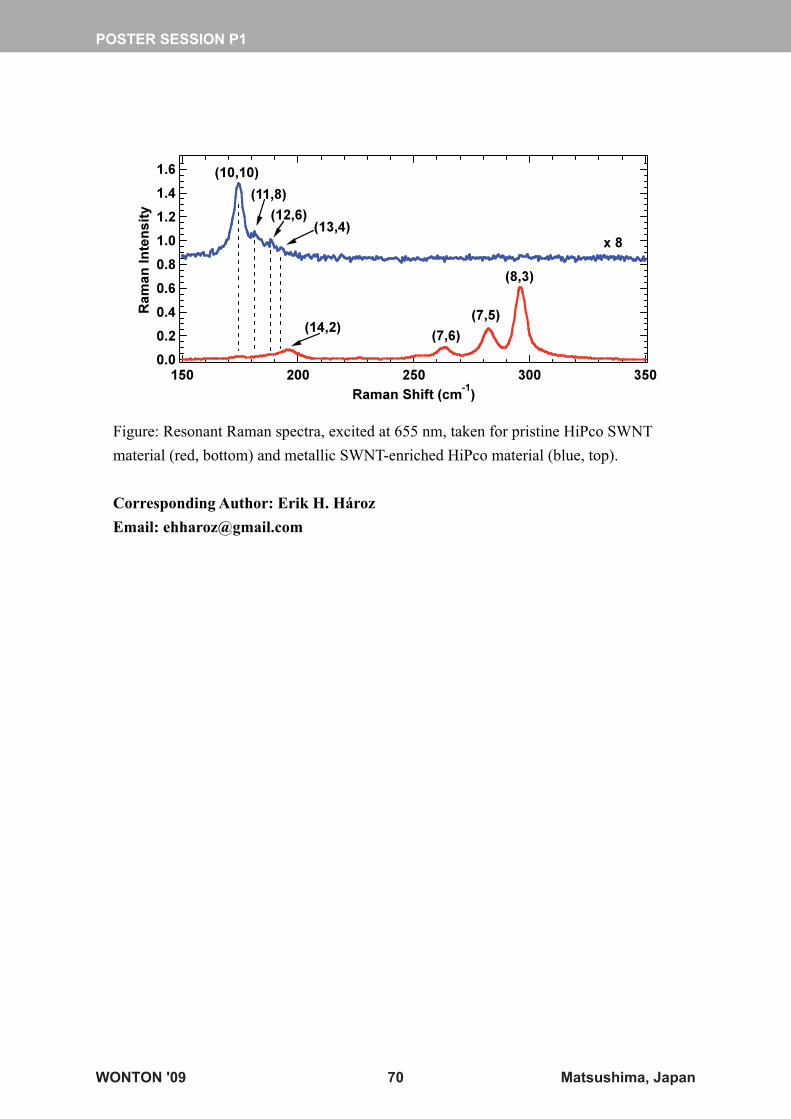
Figure: Resonant Raman spectra, excited at 655 nm, taken for pristine HiPco SWNT material (red, bottom) and metallic SWNT-enriched HiPco material (blue, top). Corresponding Author: Erik H. Hároz Email: [email protected]
POSTER SESSION P1
WONTON '09 70 Matsushima, Japan
���������������� ���������������������������������������������������������������
������ �����������������������������������������������
�������������������������!��������������
������������� ����������������������������������������������������������������������������������������������������������!"#$%#'*��/�;���
*�/����<�=����>�?�����������Q��!!*$""�*��/�;����
#�� $��$���� �� ��%� ������� *��� ���� $����� �<�>������ �*� ����>�?%�>>� !��Z��������Z���\^#_ ��{|�������%����<����*�������$������<�>�����Z��}����������������*�$�������� ����>���!�����*���� ��$$�����*�^#_ ��������}�����^� ����� ��� �������*�������� ������>� >������|����� �������������<���<�>�������*� ����$������*�^#_ ���� �������!��}������$�!�����*� ���>�����^#_ �����>�����%���������������$��Z���������>��Z�!��������}����������������*� ���� ���>�����^#_ ������>��Z��$��$�������>� ��� �����������*�^#_ ��|���$��*����^#_ �����>�����$��$�����Z��>���!�����*�������������%���������� ����?^#_ ���� ����>�� ��� ��$����?*���� ��������� ���$>�|� �$��!�>� �Z���Z��!�� �*�$�������?����������?^#_ ���%�����������Z��������������%�<�>�������*���!��������>���������� }����� �$�!���� �*� ���� ��>������ %���� �������|� ������ �������!�� !��������� �*�^#_ ���%�������!��������Z�!�������������������Z������*�^#_ ���%�����������*����Z�*�����*���� >���!�����*������|� ����� ���� }����� ���������� ������ �*� ����?�� ����$�������?^#_ ���� ���� $����� �*� $�������?^#_ ��� %��� �<�>����|� ��� ���� $�������������%�� %�>>� ��$���� ���� �����>��� ��$��������>� $����!�>�� *��� ���� ��}�����^� ������|������<����Z�����������$��������������������!�����������*��� ����$������<�>�������*�!�����!��>��<��>�Z>��^#_ ���%�>>�Z��$��������|���������|��|�������������X���|�����|�_���|�_�����\����{������|��|��|� ������������X���$�|��|��$$|�����|�!"�\����{�������|���������#���$��%��&'������%�(������������&�%�)������*����+��+/�
POSTER SESSION P2
WONTON '09 71 Matsushima, Japan
Optical Active Single-Walled Carbon Nanotubes
Naoki Komatsu,1 Xiaobin Peng,1 Feng Wang,1 Ajoy Bauri,1 A. F. M. M. Rahman,1 Takahide Kimura,1 and Atsuhiro Osuka2
1 Department of Chemistry, Shiga University of Medical Science, Seta, Otsu 520-2192
Japan 2 Department of Chemistry, Graduate School of Science, Kyoto University, Sakyo-ku,
Kyoto 606-8502, Japan
Since SWNTs were first prepared in 1993, much effort has been directed toward selective
synthesis and separation of SWNTs with limited structures or specific properties. However,
optical activity originating from carbon nanotubes themselves has been elusive. Here we
designed and synthesized chiral diporphyrins 1 – 3 shown in Fig. 1 to obtain optically active
SWNTs through molecular recognition of the
helical isomers of SWNTs [1-3].
The solutions of SWNTs extracted by (R)- and
(S)-diporphyrins (1 – 3) showed symmetrical CD
spectra, indicating that two stereoisomers (R and S)
of each diporphyrin preferentially extract SWNTs
with opposite helicities (M and P) [2] and that the
SWNTs extracted are optically active. The two
prominent CD peaks are found at 374 and 639 nm
and are assigned to E33 and E22 transitions of
(7,5)-SWNTs (Fig. 2). These spectral features
suggest much higher discrimination ability of 3 to
the helicities of (7,5)-SWNTs [3].
Acknowledgement The work is supported by
Grant-in-Aid for Scientific Research on Priority
Area of the Ministry of Education, Culture, Sports,
Science and Technology of Japan (MEXT).
References
1. X. Peng, N. Komatsu, et al., Nature Nanotechnology, 2, 361 (2007).
2. X. Peng, N. Komatsu, T. Kimura, A. Osuka, J. Am. Chem. Soc., 129, 15947 (2007).
3. X. Peng, N. Komatsu, T. Kimura, A. Osuka, ACS Nano, 2, 2045 (2008).
Corresponding Author: Naoki Komatsu, Email: [email protected]
N
N
NN
N
NN
N
Zn Zn
ArPhCH2
NHCO2t-Bu
CH2Ph
H
t-BuCO2NH HH
NHCO2t-BuPhCH2
PhCH2
NHCO2t-BuH
Ar =N
(1) (2) (3)
HN
Fig. 1 Structures of (R)-diporphyrins.
400 500 600 700
-15
-10
-5
0
5
10
15 (7,5)-SWNTs(7,5)-SWNTs
CD
In
ten
sit
y
Wavelength (nm)
Extracted with (R)-1 Extracted with (S)-1
374 nm
639 nm
Fig. 2 CD spectra of SWNTs extracted
with (R)- and (S)-diporphyrins 3.
POSTER SESSION P3
WONTON '09 72 Matsushima, Japan
Optical characterization of Length-Separated DNA-Wrapped Double-Wall Carbon Nanotubes
Yuki Asada, Shota Kuwahara, Toshiki Sugai*, Ryo Kitaura, and Hisanori Shinohara
Department of Chemistry & Institute for Advanced Research, Nagoya University, Furo-cho, Chikusa-ku, Nagoya 464-8602, Japan
Carbon nanotubes (CNTs) have unique structural, electronic and mechanical properties. Recently, double-wall carbon nanotubes (DWNTs) have attracted much attention because of their unique properties compared to single-wall carbon nanotubes (SWNTs) and multiwall carbon nanotubes (MWNTs). DNA-wrapped CNTs (DNA-CNTs) have been known to exhibit unique characteristics in their structures as well as the high solubility in pure water, and separations on the chirality and length have been achieved. Separation of CNTs by structure is very important for their utilization. We have reported the synthesis and characterization of isolated DNA-SWNTs by using natural DNA from salmon in aqueous solutions [1]. Here, we report detailed studies on the separation and the optical characterization of length separated DNA-CNTs, and we compare the dependence on the length and layer-layer interaction between SWNTs and DWNTs.
DNA-CNTs were separated by high performance liquid chromatography (HPLC) with COSMOSIL CNT (SEC 300, 1000 and 2000) columns. Fractions were collected at 1 min intervals and the lengths of DNA-CNTs were determined by AFM observation.
Fig. 1 shows the AFM images of DNA-DWNTs after separation. The average lengths of each image are 378 54, 202 34, 100 20 and 51 15 nm. PL and Raman spectra of the separated DNT- DWNTs will also be presented.
Acknowledgement The authors thank Dr. M. Yoshikawa and Mr. K. Sato of Chemical Research Laboratories, Toray Industries, Inc. for preparation of DWNTs.
* Present address: Department of Chemistry, Toho University
References 1. Y. Asada, H. Dohi, S. Kuwahara, T. Sugai, R. Kitaura, H. Shinohara, Nano 2, 295 (2007).
Corresponding Author: Hisanori ShinoharaEmail: [email protected]
Fig. 1 AFM images of variety lengths of the DNA-DWNTs. The scale bars: 500 �m
POSTER SESSION P4
WONTON '09 73 Matsushima, Japan
Resonance Raman Spectra of Optical Purified (6,5) Nanotubes Sorted by Density Gradient Ultracentrifugation
�Pei Zhao, Theerapol Thurakitseree, Erik Einarsson, Junichiro Shiomi, Shigeo Maruyama
Department of Mechanical Engineering, The University of Tokyo
We present a protocol to selectively isolate single-walled carbon nanotubes (SWNTs) with a chirality of (6,5) using density gradient ultracentrifugation (DGU)[1]. Starting with SWNTs synthesized by the alcohol catalytic chemical vapor deposition (ACCVD) method, we used sodium deoxycholate (DOC), sodium dodecyl sulfate (SDS) and sodium cholate (SC) as co-surfactant encapsulating agents[2] to isolate (6,5) SWNTs. Successful isolation was determined by photoluminescence excitation (PLE) maps, which show only one feature corresponding to (6,5). However, additional spectroscopic data (Fig. 1) such as resonance Raman spectra (488 nm laser excitation) and optical absorbance, as well as transmission electron microscopy (TEM) observation before and after the DGU process show that the sample contained a high relative purity of (6,5) SWNTs, but other chiralities were still present at low concentrations. Some evidence of their existence can be seen in optical absorbance spectra, but resonance Raman spectra using different excitation energies clearly reveal the existence of these minority species. This shows that resonance Raman spectroscopy is a more sensitive too for determining the purity of optically isolated SWNT samples, and we hope that iterated refinement of our DGU process can lead to successful extraction of single-chirality SWNTs.
Figure 1: Resonance Raman spectra (left, 488 nm laser excitation) and optical absorbance spectra (right) before and after DGU process showing selective isolation of optically purified (6,5) SWNTs from pristine ACCVD samples. [1] M. Arnold, A. Green, J. Hulvat, S. Stupp and M. Hersam. Nat. Nanotechnol. 1, 60 (2006) [2] K.Yanagi, Y. Miyata and H.Kataura, Appl. Phys. Express 1, 034003 (2008)
Corresponding Author: Shigeo Maruyama TEL: +81-3-5841-6421, FAX: +81-3-5841-6983, E-mail: [email protected]
POSTER SESSION P5
WONTON '09 74 Matsushima, Japan
Diameter distribution analysis of sorted double wall carbon nanotubes by optical absorption spectroscopy and electron
transmission microscopy.
Romain Fleurier1, Jean-Sébastien Lauret2, Emmanuel Flahaut3 and Annick Loiseau1
1LEM, ONERA 29 avenue de la division Leclerc, Châtillon, France 2LPQM, ENS Cachan 61, avenue du Président Wilson 94235 Cachan, France
3CIRIMAT/LCMIE, univ. Paul Sabatier118 Route de Narbonne 31062 Toulouse, France
Carbon nanotubes and also other nanostructures can be now separated by gradient
density ultracentrifugation methods. These techniques offer a unique opportunity to
improve our understanding of optical properties of species which are not very well
separated as synthesized and to relate them quantitatively to their structural
characteristics such as helicity and diameter. This knowledge will in turn open the
possibility to use optical spectroscopy as a reliable tool for evaluating the structure
distribution of a macroscopic sample. However optical response can be biased by
several effects such as surfactants and its relationship to the tube structure needs a
independent and direct determination of this latter.
Transmission electron microscopy, on the counterpart, provides direct measurements of
the tube characteristics such as diameter distribution, number of walls and helicity (1).
In this presentation, we propose TEM analyses as a convenient and reliable way to
evaluate and quantify the structural sorting of both single- (SWNT) and double
(DWNT)-walled nanotubes. We show that thanks to a statistical analysis of high
resolution images, one can determine the tube diameter distribution and its standard
deviation (1). In particular, we have applied the gradient centrifugation technique to a
sample containing SWNT and DWNT of different diameters and have evaluated the
efficiency of the technique for separating both kinds of tubes as well as the diameter
sorting of each kind. We will discuss how these data are related to optical absorption
spectra recorded on the same sorted samples in order to evaluate the response of this
technique to a known sample.
References
1. R. Fleurier et al, Adv.Func.Mater. 2009, In press
Corresponding Author: Romain Fleurier
Email: [email protected]
POSTER SESSION P6
WONTON '09 75 Matsushima, Japan
Polarized Raman spectroscopy on vertically aligned single-walled carbon nanotubes
Zhengyi Zhang1, Yoichi Murakami2, Erik Einarsson2, Yuhei Miyauchi3 and Shigeo Maruyama2
1Department of Mechanical Engineering, Columbia University,
New York, NY 10027, USA2Department of Mechanical Engineering, The University of Tokyo,
7-3-1 Hongo, Bunkyo-ku, Tokyo 113-8656, Japan 3Institute for Chemical Research, Kyoto University,
Gokasho, Uji, Kyoto 611-0011, Japan
Vertically aligned single-walled carbon nanotube (VA-SWNT) films with high purity have been prepared up to 30 �m thick by the alcohol catalytic chemical vapor deposition (CVD) method[1][2]. In a previous polarized Raman spectroscopy study, we found anomalous anisotropic peaks such as at 180 cm-1 for the excitation by 488 nm laser and explained them as perpendicularly polarized excitation [3]. However, recent high resolution Raman spectrum shows that the strong 180 cm-1 peak is comprised by four fine sharp peaks which might be from isolated SWNTs. To clarify its origin, polarized Raman experiment is carried out using two configurations, where the orientation of the polarizer for inspecting the scattered light was parallel to (VV) and perpendicular to (VH) the polarization of the incident light. By changing the incident light orientation with respect to the VA-SWNT growth direction, two different polarization dependences were found for the radial breathing mode (RBM) peaks. The peaks at 160 and 203 cm-1 behave consistently with the parallel excitation, while peaks at 145, 181, 244, and 256 cm-1 exhibit the opposite behavior in the VV configuration. Although the selection rules for Raman scattering process allow perpendicularly polarized excitation in RBM (A mode) [4], 181cm-1 group peaks deviate much from the theoretical calculation assuming the orientation distribution by the order parameter obtained from absorption measurements[5]. The 181 cm-1 group intensities were further revised by taking into account of laser heating effect, which show that they tend to be constant and independent for different polarization angles. Moreover, it is observed from high resolution SEM image that some isolated tubes distribute among the array which may correspond to the abnormal behaviors in CNTs.
POSTER SESSION P7
WONTON '09 76 Matsushima, Japan
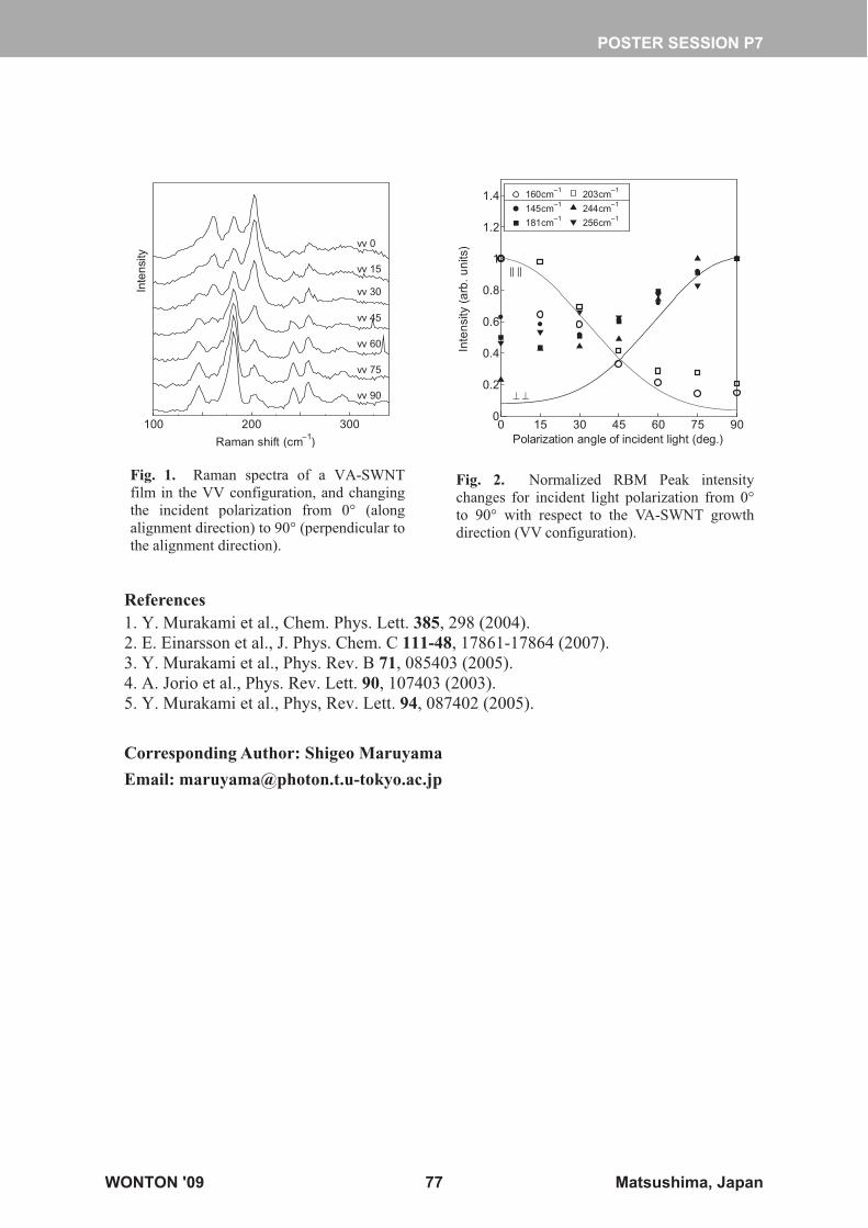
References 1. Y. Murakami et al., Chem. Phys. Lett. 385, 298 (2004). 2. E. Einarsson et al., J. Phys. Chem. C 111-48, 17861-17864 (2007). 3. Y. Murakami et al., Phys. Rev. B 71, 085403 (2005). 4. A. Jorio et al., Phys. Rev. Lett. 90, 107403 (2003). 5. Y. Murakami et al., Phys, Rev. Lett. 94, 087402 (2005).
Corresponding Author: Shigeo Maruyama Email: [email protected]
100 200 300
Raman shift (cm–1)
vv 90
vv 75
vv 60
vv 45
vv 30
vv 15
vv 0
Inte
nsity
Fig. 1. Raman spectra of a VA-SWNT film in the VV configuration, and changing the incident polarization from 0° (along alignment direction) to 90° (perpendicular to the alignment direction).
0 15 30 45 60 75 900
0.2
0.4
0.6
0.8
1
1.2
1.4
Polarization angle of incident light (deg.)
145cm–1160cm–1
181cm–1
203cm–1
244cm–1
256cm–1
Inte
nsity
(ar
b. u
nits
)
|| ||
���
Fig. 2. Normalized RBM Peak intensity changes for incident light polarization from 0° to 90° with respect to the VA-SWNT growth direction (VV configuration).
POSTER SESSION P7
WONTON '09 77 Matsushima, Japan
High-Precision Selective Deposition of Catalyst for Facile Localized Growth of Single Walled Carbon Nanotubes
Rong Xiang1, Tianzhun Wu1, Erik Einarsson1, Yuji Suzuki1, Yoichi Murakami1,2,
Junichiro Shiomi1, Shigeo Maruyama1
1Department of Mechanical Engineering, The University of Tokyo, Tokyo
113-8656, Japan 2Global Edge Institute, Tokyo Institute of Technology, Tokyo 152-8550, Japan
In the liquid-based dip-coating, hydrophilicity of Si/SiO2 substrate is found to be
critical for the successful deposition of catalyst and hence the growth of single-walled
carbon nanotubes (SWNTs). When the surface is functionalized by self-assembly
monolayer (SAM) and becomes hydrophobic, no catalyst remains and no SWNT grows.
This concept can be utilized to localize the growth of SWNTs at designed regions where
SAM were selectively removed by, e.g. UV or electron beam. The advantage of the
proposed technique comparing to conventional M/NEMS technique (e.g. lift-offf) is as
followings. Firstly, the resolution can be expected to be very high, and a SWNT pattern
with the line-wide of 50 nm can be easily obtained. Secondly, the ability of damaging
SAM by electron beam in an SEM makes the localization process visible, which
facilitates the fabrication of devices basing on as-grown high-quality SWNTs. Examples
will be demonstrated.[1]
References
[1] R. Xiang, T. Wu, E. Einarsson, Y. Suzuki, Y. Murakami, J. Shiomi, S. Maruyama,
High-Precision Selective Deposition of Catalyst for Facile Localized Growth of Single
Walled Carbon Nanotubes, submitted.
Corresponding Author: Shigeo Maruyama
Email: [email protected]
POSTER SESSION P8
WONTON '09 78 Matsushima, Japan
Raman and optical spectroscopic analysis of single walled carbonnanotubes synthesized by an industrial scale aerosol reactor
Ying Tian1, Albert G Nasibulin1, Hua Jiang1, Timur Nikitin2, Brad Aitchison3, Jan VPfaler4, Leonid Khriachtchev2, Jussi O Sarkkinen3, David P Brown3, Esko I
Kauppinen1,5
1 NanoMaterials Group, Department of Applied Physics and Center for New Materials,Helsinki University of Technology, P.O. Box 5100, FIN-02150, Espoo, Finland
2Laboratory of Physical Chemistry,Department of Chemistry, University of Helsinki,P.O. Box 55, FIN-00014 Helsinki, Finland3Canatu Ltd, FIN-02150, Espoo, Finland
4Department of Mathematics and Systems analysis, Helsinki University of Technology,Espoo, Finland
5VTT Biotechnology, Espoo, Finland
Abstract Carbon nanotubes, and in particular Single walled carbon nanotubes(SWCNTs), have attracted a great interest due to their remarkable properties, whichhave been utilized in many different applications such as sensors, transistors,optoelectronic devices, composites with enhanced properties and for energy storage. Itis well known that the properties of SWCNTs can significantly vary depending on theirdiameters and chiral angles. Therefore, it is crucial to tailor the size distribution of theSWCNTs to fit the requirement for specific applications.
In this work, detailed parametric analysis of SWCNTs synthesized in an industrial scaleaerosol method was carried out. The sample morphology, mean diameter, diameterdistribution as well as the relative nanotube abundance of the SWCNTs were analyzedby a combined study of transmission electron microscopy, Raman and opticalabsorption spectroscopy. The results show that increased growth temperature results inan increase in SWCNT mean diameter. The CO2 plays an essential role in the SWCNTsgrowth process as an etching agent. The addition of small amounts of CO2 increases themean diameter of SWCNTs and improves the purity of SWCNTs. Moreover, theresident time and the concentration of catalyst were varied by changing the flow rate ofCO, which also affects the diameter distribution of the SWCNTs production. Theseresults show that the SWCNTs diameter, diameter distribution and purity can be variedas a function of reactor conditions, which is important to meet requirements of variousapplications.
POSTER SESSION P9
WONTON '09 79 Matsushima, Japan
Effects of Bundling and Diameter on the UV Optical Absorption of Single-Wall Carbon Nanotubes
Takeshi Saito1,2, Shigekazu Ohmori1, Bikau Shukla1, Motoo Yumura1 and Sumio Iijima1
1Nanotube Research Center, AIST, Tsukuba 305-8565, Japan 2PRESTO, Japan Science and Technology Agency, Kawaguchi 332-0012, Japan
Introduction: Optical absorption spectroscopy has been frequently used as one of the most powerful tool for the characterizations of purity [1], metal/semiconductor ratio [2], and diameters of single-wall carbon nanotubes (SWCNTs) [3]. In general, peaks analyzed for these characterizations are observed in near infrared (NIR) region and can be assigned to the interband transitions between van Hove singularities. On the other hand, the ultraviolet absorption which is largest part of optical absorption of SWCNTs have not been fully investigated, probably due to the analytical difficulty arisen from overlapped pi plasmon absorption of graphitic impurities. The pi plasmon absorption is extremely broad and is superposed on the NIR absorption peaks as a featureless background in NIR region. It has been pointed out that the intensity ratio between the NIR absorption peaks and the background increases as bundles of SWCNTs are exfoliated, although this mechanism has not yet been clarified.
In this work, we have investigated the variation of UV optical absorption of SWCNTs on the different degree of their bundling. Moreover, we have prepared three samples with different SWCNT diameter ranges and discussed the diameter dependence of UV optical absorptions.Experimental: SWCNTs synthesized by the gas-phase CVD growth, e-DIPS method [3], were dispersed in D2O containing 1 wt% of sodium cholate by using a tip ultrasonic homogenizer (SONICS VCX500) equipped with a titanium alloy tip (TI-6AL-4V). Pulsed sonication was applied (on: 1 sec, off: 2 sec) with a power of 200 W for 30 min. In order to prepare SWCNT dispersions with different degree of bundling, each dispersed solution was then centrifuged at 127600 ×g for 0.5, 1.0 and 2.5 hrs (Hitachi CP 100MX with a P56ST swing rotor) and the supernatant of the upper ca. 80 % of the volume was collected and subjected to the optical absorption measurements. Results and Discussion: Optical absorption spectra of SWCNT dispersions prepared by different centrifugation times, 0.5, 1.0 and 2.5 hrs are shown in Figure 1A. Optical absorption observed in NIR region became weaker but sharper as the elongation of centrifugation time, although shapes of that were basically maintained. Because the
POSTER SESSION P10
WONTON '09 80 Matsushima, Japan
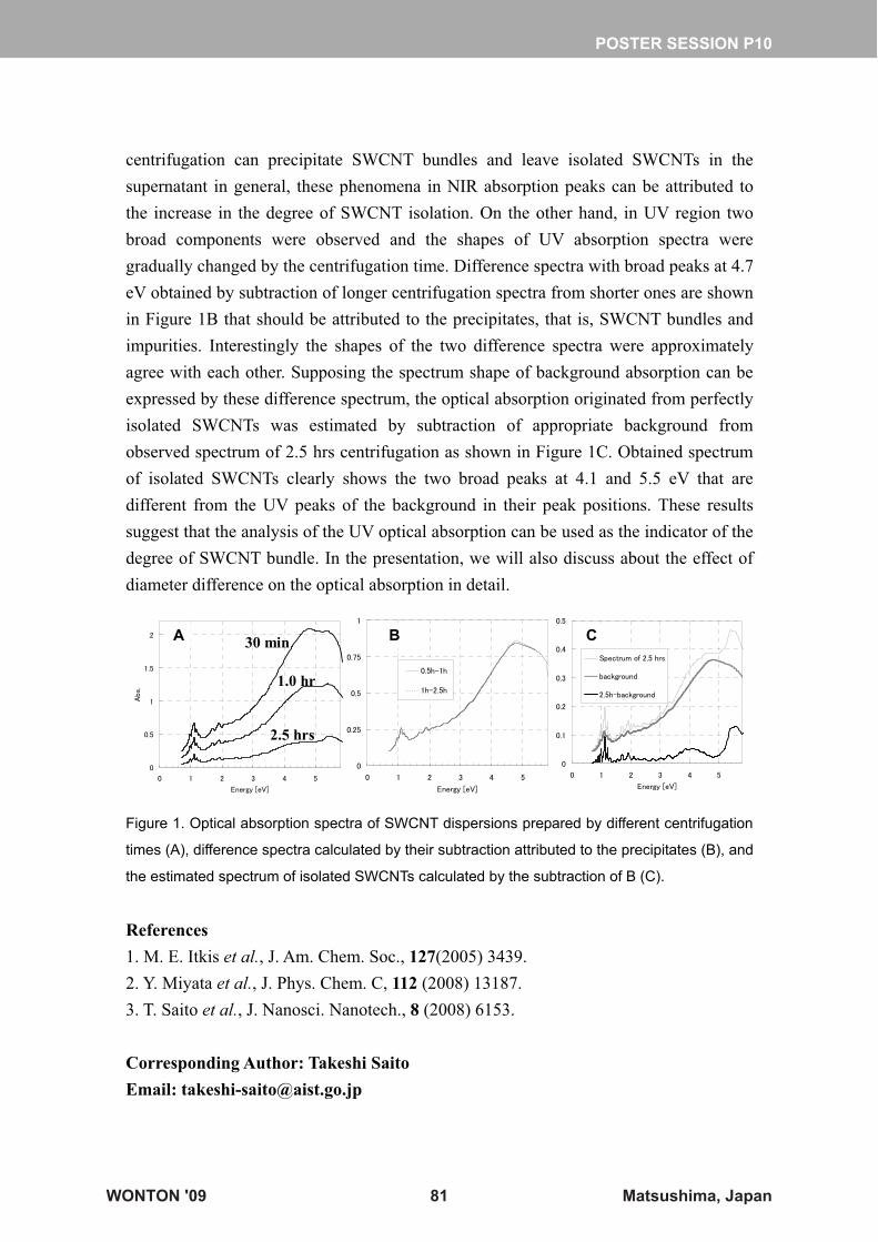
centrifugation can precipitate SWCNT bundles and leave isolated SWCNTs in the supernatant in general, these phenomena in NIR absorption peaks can be attributed to the increase in the degree of SWCNT isolation. On the other hand, in UV region two broad components were observed and the shapes of UV absorption spectra were gradually changed by the centrifugation time. Difference spectra with broad peaks at 4.7 eV obtained by subtraction of longer centrifugation spectra from shorter ones are shown in Figure 1B that should be attributed to the precipitates, that is, SWCNT bundles and impurities. Interestingly the shapes of the two difference spectra were approximately agree with each other. Supposing the spectrum shape of background absorption can be expressed by these difference spectrum, the optical absorption originated from perfectly isolated SWCNTs was estimated by subtraction of appropriate background from observed spectrum of 2.5 hrs centrifugation as shown in Figure 1C. Obtained spectrum of isolated SWCNTs clearly shows the two broad peaks at 4.1 and 5.5 eV that are different from the UV peaks of the background in their peak positions. These results suggest that the analysis of the UV optical absorption can be used as the indicator of the degree of SWCNT bundle. In the presentation, we will also discuss about the effect of diameter difference on the optical absorption in detail.
30 min
1.0 hr
2.5 hrs
A B C30 min
1.0 hr
2.5 hrs
A B C
Figure 1. Optical absorption spectra of SWCNT dispersions prepared by different centrifugation
times (A), difference spectra calculated by their subtraction attributed to the precipitates (B), and
the estimated spectrum of isolated SWCNTs calculated by the subtraction of B (C).
References 1. M. E. Itkis et al., J. Am. Chem. Soc., 127(2005) 3439. 2. Y. Miyata et al., J. Phys. Chem. C, 112 (2008) 13187. 3. T. Saito et al., J. Nanosci. Nanotech., 8 (2008) 6153.
Corresponding Author: Takeshi SaitoEmail: [email protected]
POSTER SESSION P10
WONTON '09 81 Matsushima, Japan
Fermi energy dependence of radial breathing mode in metallic single-wall carbon nanotubes
* Jin Sung Park1), Kenich Sasaki2), Riichiro Saito1), Gene Dressselhaus3), Mildred S. Dresselhaus3)
1) Tohoku University, Japan, 2) Hiroshima University, Japan, 3) Massachusetts Institute of Technology, Cambridge, MA 02139-4307, USA
The radial breathing mode (RBM) of single-wall carbon nanotubes (SWNTs) arises from the first-order, one-phonon and intra-valley Raman scattering process, which is used to assign the diameter and chirality of a SWNT. For metallic SWNTs, the curvature effect induces a small energy gap except for armchair SWNTs. Since the curvature-induced energy gap is similar to the RBM phonon energy for nanotubes with diameter range, 0.7<dt<2 nm (15~40 meV), the curvature-induced energy gap may affect the phonon softening of the RBM, so called the Kohn anomaly effect. The Kohn anomaly effect can be explained by the self-energy correction to the RBM phonon mode in which the virtual excitation of an electron-hole pair causes a softening of the RBM phonon frequencies. Recently a n experimental group ha s observed the Fermi energy (EF)dependence of the phonon-softening effect of M-SWNTs by electrochemical doping, and their result clearly shows the RBM phonon softening as a function of EF [1]. The frequency shift of the RBM is produced by electron-phonon interaction [2]. The RBM Raman spectrum for the M-SWNTs depends on chirality and diameter. While a zigzag SWNT shows the maximum RBM frequency shift, an armchair SWNT does now show any frequency shift. It has been known that the k-electron-phonon (el-ph) interaction of the RBM gives rise to the chirality dependence [3]. Although the RBM Raman intensity has been calculated by the el-ph and electron-photon (el-op) interactions, the RBM Raman spectrum has not been calculated yet. In this poster, the RBM Raman spectrum will be shown by including the Kohn anomaly effect and the resonance window values [4]. And instead of el-ph and el-op interaction for Raman intensity calculation, we will consider exciton-phonon and exciton-photon interactions. As a result, the chiral angle dependence of the RBM Raman spectrum can be directly compared to the experiment. The gate voltage dependence of the RBM Raman spectra for metallic nanotubes is also directly compared to the experiment in which the Kohn anomaly effect appears by change of the Fermi energy.
Reference:[1] H. Farhat et al., Phys. Rev. Lett., in press (2009). [2] K. Sasaki et al., Phys. Rev. B, 78, 235405 (2008). [3] J. Jiang et al., Phys. Rev. B, 72, 235408 (2005). [4] J. S. Park et al., Phys. Rev. B, 74, 165414 (2006).
Corresponding Author: Email: [email protected]
POSTER SESSION P11
WONTON '09 82 Matsushima, Japan
Exciton energy Kataura plot and excitonic effect of single wall carbon nanotubes
Kentaro Sato1, Riichiro Saito2 and Shigeo Maruyama1
1Department of Mechanical Engineering, The University of Tokyo,
7-3-1 Hongo, Bunkyo-ku, Tokyo 113-8656, Japan 2Department of Physics, Tohoku University, Aramaki, Aoba-ku, Sendai 980-8578, Japan
We calculate exciton energy of single wall carbon nanotubes (SWNTs). The exciton
energy depends on the surrounding materials of the SWNT [1]. This environmental
effect is expressed by the dielectric constant [2]. In previous paper we used the static
dielectric constant in order to reproduce the resonance Raman experiment for bundle
samples [3,4]. However, since the dielectric constant depends on the nanotube diameter
[5] and the surrounding materials, we need to consider a correction to the environmental
effect for other samples. In this paper we discuss the environmental effect of SWNTs.
The exciton energy of SWNTs is calculated by solving the Bethe-Salpeter equation in
which the one particle energies are given by the extended tight-binding scheme [3]. We
also compare our calculation with the resonance Raman experiments in the different
environment. From our calculation we show the exciton energy Kataura plot for
different samples.
References
1. V. C. Moore et al., Nano Lett. 3, 1379 (2003).
2. T. Ando, J. Phys. Soc. Jpn. 66. 1066 (1997).
3. J. Jiang et al., Phys. Rev. B 75, 035407 (2007).
4. K. Sato et al., Phys. Rev. B 76, 195446 (2007).
5. Y. Miyauchi et al., Chem. Phys. Lett. 442, 394 (2007).
Corresponding Author: Kentaro Sato
Email: [email protected]
POSTER SESSION P12
WONTON '09 83 Matsushima, Japan
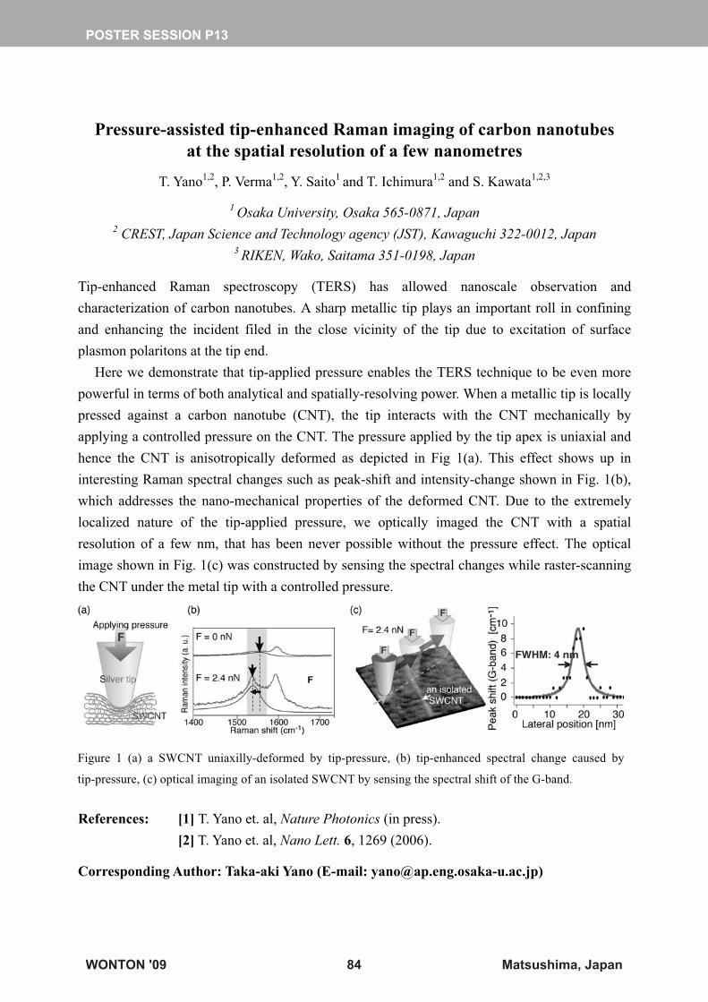
Pressure-assisted tip-enhanced Raman imaging of carbon nanotubes
at the spatial resolution of a few nanometres
T. Yano1,2
, P. Verma1,2
, Y. Saito1
and T. Ichimura1,2
and S. Kawata1,2,3
1 Osaka University, Osaka 565-0871, Japan
2 CREST, Japan Science and Technology agency (JST), Kawaguchi 322-0012, Japan
3 RIKEN, Wako, Saitama 351-0198, Japan
Tip-enhanced Raman spectroscopy (TERS) has allowed nanoscale observation and
characterization of carbon nanotubes. A sharp metallic tip plays an important roll in confining
and enhancing the incident filed in the close vicinity of the tip due to excitation of surface
plasmon polaritons at the tip end.
Here we demonstrate that tip-applied pressure enables the TERS technique to be even more
powerful in terms of both analytical and spatially-resolving power. When a metallic tip is locally
pressed against a carbon nanotube (CNT), the tip interacts with the CNT mechanically by
applying a controlled pressure on the CNT. The pressure applied by the tip apex is uniaxial and
hence the CNT is anisotropically deformed as depicted in Fig 1(a). This effect shows up in
interesting Raman spectral changes such as peak-shift and intensity-change shown in Fig. 1(b),
which addresses the nano-mechanical properties of the deformed CNT. Due to the extremely
localized nature of the tip-applied pressure, we optically imaged the CNT with a spatial
resolution of a few nm, that has been never possible without the pressure effect. The optical
image shown in Fig. 1(c) was constructed by sensing the spectral changes while raster-scanning
the CNT under the metal tip with a controlled pressure.
References: [1] T. Yano et. al, Nature Photonics (in press).
[2] T. Yano et. al, Nano Lett. 6, 1269 (2006).
Corresponding Author: Taka-aki Yano (E-mail: [email protected])
Figure 1 (a) a SWCNT uniaxilly-deformed by tip-pressure, (b) tip-enhanced spectral change caused by
tip-pressure, (c) optical imaging of an isolated SWCNT by sensing the spectral shift of the G-band.
POSTER SESSION P13
WONTON '09 84 Matsushima, Japan
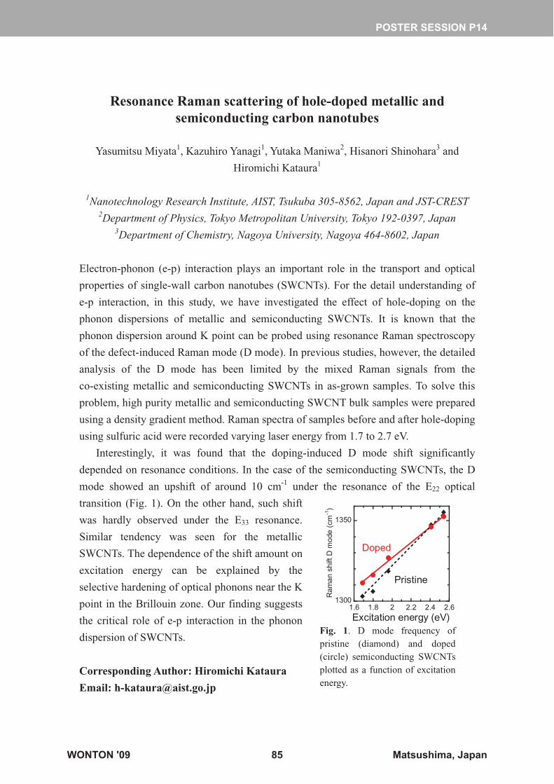
Resonance Raman scattering of hole-doped metallic and semiconducting carbon nanotubes
Yasumitsu Miyata1, Kazuhiro Yanagi1, Yutaka Maniwa2, Hisanori Shinohara3 and
Hiromichi Kataura1
1Nanotechnology Research Institute, AIST, Tsukuba 305-8562, Japan and JST-CREST 2Department of Physics, Tokyo Metropolitan University, Tokyo 192-0397, Japan
3Department of Chemistry, Nagoya University, Nagoya 464-8602, Japan
Electron-phonon (e-p) interaction plays an important role in the transport and optical
properties of single-wall carbon nanotubes (SWCNTs). For the detail understanding of
e-p interaction, in this study, we have investigated the effect of hole-doping on the
phonon dispersions of metallic and semiconducting SWCNTs. It is known that the
phonon dispersion around K point can be probed using resonance Raman spectroscopy
of the defect-induced Raman mode (D mode). In previous studies, however, the detailed
analysis of the D mode has been limited by the mixed Raman signals from the
co-existing metallic and semiconducting SWCNTs in as-grown samples. To solve this
problem, high purity metallic and semiconducting SWCNT bulk samples were prepared
using a density gradient method. Raman spectra of samples before and after hole-doping
using sulfuric acid were recorded varying laser energy from 1.7 to 2.7 eV.
Interestingly, it was found that the doping-induced D mode shift significantly
depended on resonance conditions. In the case of the semiconducting SWCNTs, the D
mode showed an upshift of around 10 cm-1 under the resonance of the E22 optical
transition (Fig. 1). On the other hand, such shift
was hardly observed under the E33 resonance.
Similar tendency was seen for the metallic
SWCNTs. The dependence of the shift amount on
excitation energy can be explained by the
selective hardening of optical phonons near the K
point in the Brillouin zone. Our finding suggests
the critical role of e-p interaction in the phonon
dispersion of SWCNTs.
1300
1350
1.6 1.8 2 2.2 2.4 2.6
Excitation energy (eV)
Doped
Pristine
Ram
an s
hift
D m
ode
(cm
-1)
Fig. 1. D mode frequency of pristine (diamond) and doped (circle) semiconducting SWCNTs plotted as a function of excitation energy.
Corresponding Author: Hiromichi Kataura
Email: [email protected]
POSTER SESSION P14
WONTON '09 85 Matsushima, Japan
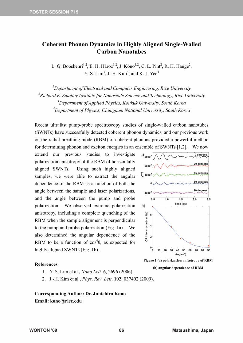
Coherent Phonon Dynamics in Highly Aligned Single-Walled Carbon Nanotubes
L. G. Booshehri1,2, E. H. Hároz1,2, J. Kono1,2, C. L. Pint2, R. H. Hauge2,
Y.-S. Lim3, J.-H. Kim4, and K.-J. Yee4
1Department of Electrical and Computer Engineering, Rice University 2Richard E. Smalley Institute for Nanoscale Science and Technology, Rice University
3Department of Applied Physics, Konkuk University, South Korea 4Department of Physics, Chungnam National University, South Korea
Recent ultrafast pump-probe spectroscopy studies of single-walled carbon nanotubes (SWNTs) have successfully detected coherent phonon dynamics, and our previous work on the radial breathing mode (RBM) of coherent phonons provided a powerful method for determining phonon and exciton energies in an ensemble of SWNTs [1,2]. We now extend our previous studies to investigate polarization anisotropy of the RBM of horizontally aligned SWNTs. Using such highly aligned samples, we were able to extract the angular dependence of the RBM as a function of both the angle between the sample and laser polarizations, and the angle between the pump and probe polarization. We observed extreme polarization anisotropy, including a complete quenching of the RBM when the sample alignment is perpendicular to the pump and probe polarization (Fig. 1a). We also determined the angular dependence of the RBM to be a function of cos4�, as expected for highly aligned SWNTs (Fig. 1b). References
1. Y. S. Lim et al., Nano Lett. 6, 2696 (2006). 2. J.-H. Kim et al., Phys. Rev. Lett. 102, 037402 (2009).
Corresponding Author: Dr. Junichiro Kono Email: [email protected]
Figure 1 (a) polarization anisotropy of RBM
(b) angular dependence of RBM
POSTER SESSION P15
WONTON '09 86 Matsushima, Japan
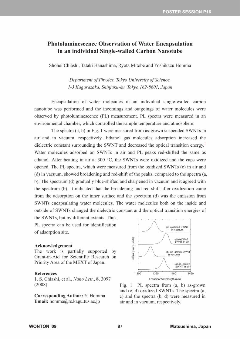
Photoluminescence Observation of Water Encapsulation in an individual Single-walled Carbon Nanotube
Shohei Chiashi, Tataki Hanashima, Ryota Mitobe and Yoshikazu Homma
Department of Physics, Tokyo University of Science,
1-3 Kagurazaka, Shinjuku-ku, Tokyo 162-8601, Japan
Encapsulation of water molecules in an individual single-walled carbon
nanotube was performed and the incomings and outgoings of water molecules were
observed by photoluminescence (PL) measurement. PL spectra were measured in an
environmental chamber, which controlled the sample temperature and atmosphere.
The spectra (a, b) in Fig. 1 were measured from as-grown suspended SWNTs in
air and in vacuum, respectively. Ethanol gas molecules adsorption increased the
dielectric constant surrounding the SWNT and decreased the optical transition energy.1
Water molecules adsorbed on SWNTs in air and PL peaks red-shifted the same as
ethanol. After heating in air at 300 �C, the SWNTs were oxidized and the caps were
opened. The PL spectra, which were measured from the oxidized SWNTs (c) in air and
(d) in vacuum, showed broadening and red-shift of the peaks, compared to the spectra (a,
b). The spectrum (d) gradually blue-shifted and sharpened in vacuum and it agreed with
the spectrum (b). It indicated that the broadening and red-shift after oxidization came
from the adsorption on the inner surface and the spectrum (d) was the emission from
SWNTs encapsulating water molecules. The water molecules both on the inside and
outside of SWNTs changed the dielectric constant and the optical transition energies of
the SWNTs, but by different extents. Thus,
PL spectra can be used for identification
of adsorption site.
Acknowledgement The work is partially supported by Grant-in-Aid for Scientific Research on Priority Area of the MEXT of Japan.
1300 1350 1400 1450
(a) as–grown SWNT in air
(c) oxidized SWNT in air
Emission Wavelength (nm)
Inte
nsity
(ar
b. u
nits
)
(b) as–grown SWNT in vacuum
(d) oxidized SWNT in vacuum
Fig. 1 PL spectra from (a, b) as-grown and (c, d) oxidized SWNTs. The spectra (a, c) and the spectra (b, d) were measured in air and in vacuum, respectively.
References 1. S. Chiashi, et al., Nano Lett., 8, 3097 (2008).
Corresponding Author: Y. Homma Email: [email protected]
POSTER SESSION P16
WONTON '09 87 Matsushima, Japan
Intrinsic and Extrinsic Factors which Affects the Optical Properties of Individual Single-Walled Carbon Nanotubes
Juan G. Duque1,2,3 Stephen Doorn1 Howard K. Schmidt2 and Matteo Pasquali2
Laurent Cognet3 and Brahim Lounis3
1Los Alamos National Laboratory, Physical Chemistry and Applied Spectroscopy P.O. Box 1663, Los Alamos, NM 875442Department of Chemical and Biomolecular Engineering, Rice University, 6100 Main Street, Houston, TX 77005
3Centre de Physique Moléculaire Optique et Hertzienne, Université de Bordeaux and CNRS, 351 cours de la libération, Talence F-33405, France.
Multiple studies have shown that the optical properties of single-walled carbon nanotubes(SWNTs) are excitonic in nature.1-3 However, a complete understanding of how these excitonic states shape the optical properties of SWNTs is lacking. Comparing the results of different published studies is difficult; the luminescence properties of SWNTs are affected by various extrinsic factors originating from synthesis and processing methods which affect the structure, sidewall quality, and environment of SWNTs. Fundamental and applied reports are hindered by poor control over the synthesis and post-processing methods. This is highlighted by the range of reported fluorescence quantum yields and luminescence lifetimes measured from ensembles or single SWNTs – they range between 10-4 to 7 %4-8 and from 5 to 200 ps,5,8-10 respectively, depending on the report.
Here we use single molecule imaging and time resolved spectroscopy,photoluminescence maps, UV-vis absorbance, and Raman spectroscopy at multiple excitation wavelengths to identify different extrinsic factors which deeply influence the optical properties of SWNT.11,12 Single molecular studies of individual (6,5) SWNTs showed that SWNT luminescence depends strongly on extrinsic and intrinsic factors such as sample preparation, sample environment, sidewall defects, and tube synthesis methods (HiPco or CoMoCat).11 More precisely, we showed that surfactant selection and sample medium are crucial factors to obtaining SWNTs with optimum optical properties.
Ensemble measurements showed compelling spectroscopic evidence of substantial differences in chirality and diameter distribution which alter the luminescence properties withindifferent HiPco batches.12 These variations also affect SWNT solubility both in surfactant suspensions and superacids. These findings underline the necessity for more standard production and post-processing procedures such that correlations between different reports in the literature can be drawn, and we begin to understand the complex excitonic structure of SWNTs.
References
1. Wang, F.; et. al Science 2005, 308, (5723), 838. 2. Perebeinos, et. al. PRL 2004, 92, (25 I), 257402.3. Shaver, J.; et.al. Nano Lett. 2007, 7, (7), 1851.4. O'Connell, M. J.; et.al. Science 2002, 297, (5581), 593.5. Wang, F.; et.al. Nano Lett. 2007, 7, (12), 3698-3703.7. Tsyboulski, D. A.; et.al. Nano Lett. 2007, 7, (10), 3080.
8. Berciaud, S.; et.al. PRL 2008, 101, (7), 077402.9. Jones, M.; et.al. Phys. Rev. B 2005, 71, 115426.10. Hirori, H.; et.al. PRL 2006, 97, (25), 257401.11. Duque, J. G.; et.al. Nano Lett.; Submitted.12. Duque, J. G.; et.al. In Preparation.
JGD: [email protected] Phone: 713-817-9796
POSTER SESSION P17
WONTON '09 88 Matsushima, Japan
Electrochemistry and Self-Assembly of Complex Single-Walled Carbon Nanotube (SWNT) Nanostructures
Juan G. Duque1,2, Laurent Cognet3, Howard K. Schmidt2, Matteo Pasquali2
1Los Alamos National Laboratory, Physical Chemistry and Applied Spectroscopy P.O. Box 1663, Los Alamos, NM 875442Department of Chemical and Biomolecular Engineering, Rice University, 6100 Main Street, Houston, TX 77005
3Centre de Physique Moléculaire Optique et Hertzienne, Université de Bordeaux and CNRS, 351 cours de la libération, Talence F-33405, France.
This work explores the optical and electrochemical properties of surfactant stabilized and individually-suspended SWNTs in aqueous media via application of various external stimuli. As a result, novel nanostructures are obtained, and this allows for the study of the inherent nanotube electronic and optical properties. The goal is to engineer SWNT systems which can be tuned by understanding the mechanism of the electrochemical and environmental reactions so that applications in nanophotonics, photovoltaics, and electronics can be effectively exploited.
A strategy to obtain a surfactant/polymer protective “shell" that improves the stability and luminescence signal of individual SWNTs is presented. We used literature evidence of fluorescence emission shifts to understand the interactions between polymers and surfactants and show how morphological changes induced by extrinsic factors distort the SWNT luminescence. We developed an in-situ polymerization which creates an outer shell around the SWNT micelle that resulted in suspensions with stable luminescence at all pH, in saline buffers, and on the surface of living cells.1
Nanoparticle-nanotube structures were also fabricated by exploiting the electrochemical properties of SWNTs upon activation with alternating electromagnetic fields (EM). Under EM, metallic SWNTs will preferentially polarize creating a localized apparent field enhancement at the tips due to their high aspect ratio and electronic properties -antenna behavior. This field enhancement can generate sufficient current densities which drive electron transfer reactions preferentially at their tips, reducing transition metal salts into nanoparticles. The selectivity is assessed using microscopic and spectroscopic techniques such as atomic force microscopy, UV-vis absorbance, and Raman spectroscopy. At the end we obtain a system with tunable reactionconditions where spontaneous particle formations are controlled and selective deposition is obtained to form novel nanostructures.2
References
1. Duque, J.; et, al; JACS, 2008, 130, (8), 2626 2. Duque, J.; et, al; JACS, 2008, 130, (46), 15340
JGD: [email protected] Phone: 713-817-9796
POSTER SESSION P18
WONTON '09 89 Matsushima, Japan
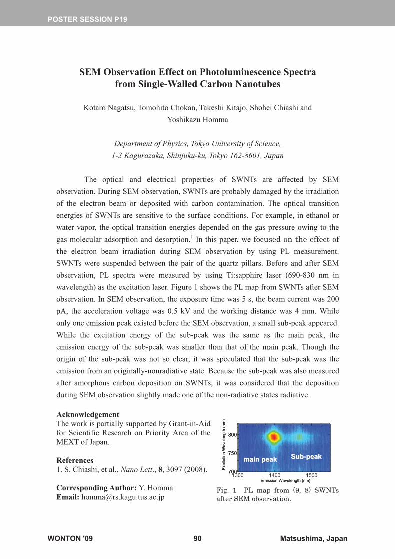
SEM Observation Effect on Photoluminescence Spectra from Single-Walled Carbon Nanotubes
Kotaro Nagatsu, Tomohito Chokan, Takeshi Kitajo, Shohei Chiashi and
Yoshikazu Homma
Department of Physics, Tokyo University of Science,
1-3 Kagurazaka, Shinjuku-ku, Tokyo 162-8601, Japan
The optical and electrical properties of SWNTs are affected by SEM
observation. During SEM observation, SWNTs are probably damaged by the irradiation
of the electron beam or deposited with carbon contamination. The optical transition
energies of SWNTs are sensitive to the surface conditions. For example, in ethanol or
water vapor, the optical transition energies depended on the gas pressure owing to the
gas molecular adsorption and desorption.1 In this paper, we focused on the effect of the electron beam irradiation during SEM observation by using PL measurement.
SWNTs were suspended between the pair of the quartz pillars. Before and after SEM
observation, PL spectra were measured by using Ti:sapphire laser (690-830 nm in
wavelength) as the excitation laser. Figure 1 shows the PL map from SWNTs after SEM
observation. In SEM observation, the exposure time was 5 s, the beam current was 200
pA, the acceleration voltage was 0.5 kV and the working distance was 4 mm. While
only one emission peak existed before the SEM observation, a small sub-peak appeared.
While the excitation energy of the sub-peak was the same as the main peak, the
emission energy of the sub-peak was smaller than that of the main peak. Though the
origin of the sub-peak was not so clear, it was speculated that the sub-peak was the
emission from an originally-nonradiative state. Because the sub-peak was also measured
after amorphous carbon deposition on SWNTs, it was considered that the deposition
during SEM observation slightly made one of the non-radiative states radiative.
Acknowledgement
1300 1400 1500700
750
800
Emission Wavelength (nm)
Exc
itatio
n W
avel
engt
h (n
m)
main peakmain peak SubSub--peakpeak
1300 1400 1500700
750
800
Emission Wavelength (nm)
Exc
itatio
n W
avel
engt
h (n
m)
main peakmain peak SubSub--peakpeak
1300 1400 1500700
750
800
Emission Wavelength (nm)
Exc
itatio
n W
avel
engt
h (n
m)
main peakmain peak SubSub--peakpeak
Fig. 1 PL map from (9, 8) SWNTs after SEM observation.
The work is partially supported by Grant-in-Aid for Scientific Research on Priority Area of the MEXT of Japan.
References 1. S. Chiashi, et al., Nano Lett., 8, 3097 (2008).
Corresponding Author: Y. Homma Email: [email protected]
POSTER SESSION P19
WONTON '09 90 Matsushima, Japan
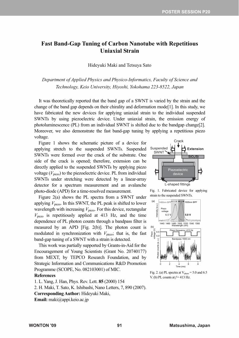
Fast Band-Gap Tuning of Carbon Nanotube with Repetitious Uniaxial Strain
Hideyuki Maki and Tetsuya Sato
Department of Applied Physics and Physico-Informatics, Faculty of Science and
Technology, Keio University, Hiyoshi, Yokohama 223-8522, Japan
It was theoretically reported that the band gap of a SWNT is varied by the strain and the change of the band gap depends on their chirality and deformation mode[1]. In this study, we have fabricated the new devices for applying uniaxial strain to the individual suspended SWNTs by using piezoelectric device. Under uniaxial strain, the emission energy of photoluminescence (PL) from an individual SWNT is shifted due to the bandgap change[2]. Moreover, we also demonstrate the fast band-gap tuning by applying a repetitious piezo voltage. Figure 1 shows the schematic picture of a device for applying stretch to the suspended SWNTs. Suspended SWNTs were formed over the crack of the substrate. One side of the crack is opened; therefore, extension can be directly applied to the suspended SWNTs by applying piezo voltage (Vpiezo) to the piezoelectric device. PL from individual SWNTs under stretching were detected by a linear-array detector for a spectrum measurement and an avalanche photo-diode (APD) for a time-resolved measurement. Figure 2(a) shows the PL spectra from a SWNT under applying Vpiezo. In this SWNT, the PL peak is shifted to lower wavelength with increasing Vpiezo. For this device, rectangular Vpiezo is repetitiously applied at 413 Hz, and the time dependence of PL photon counts through a bandpass filter is measured by an APD [Fig. 2(b)]. The photon count is modulated in synchronization with Vpiezo; that is, the fast band-gap tuning of a SWNT with a strain is detected. This work was partially supported by Grants-in-Aid for the Encouragement of Young Scientists (Grant No. 20740177) from MEXT, by TEPCO Research Foundation, and by Strategic Information and Communications R&D Promotion Programme (SCOPE, No. 082103001) of MIC. References 1. L. Yang, J. Han, Phys. Rev. Lett. 85 (2000) 154 2. H. Maki, T. Sato, K. Ishibashi, Nano Letters, 7, 890 (2007). Corresponding Author: Hideyuki Maki, Email: [email protected]
Piezoelectricdevice
L-shaped fittings
ExtensionSuspendedSWNT
22SiO /SiSiO /Si
Crack
Fig. 1. Fabricated device for applying strain to the suspended SWNTs.
1480nm BPF 1505nm BPF
Piezovoltage
6.5 V 5.0 V
1560154015201500148014601440Wavelength (nm)
Inte
nsity
(a.u
.)
86420Time (ms)
Phot
on c
ount
s (a
. u.) Bandpass 1505 nm
Piezo frequency: 413 Hz
Pie
zovo
ltage
(V)
6.5
5.0
(a)
(b)
Fig. 2. (a) PL spectra at Vpiezo = 5.0 and 6.5 V. (b) PL counts at f = 413 Hz.
POSTER SESSION P20
WONTON '09 91 Matsushima, Japan
An Optical Study of a Single Carbon Nanotube
X. Wang, M. Hadjipanayi, R. J. Nicholas and R. A. Taylor
Clarendon Laboratory, Physics Department, University of Oxford,
Parks Road, Oxford, OX1 3PU, United Kingdom
Abstract � We study the photoluminescence from single carbon nanotubes.
Single-walled carbon nanotubes (SWNTs) have attracted great interest in the last decade
following and great strides have been made in understanding their collective optical
properties. However, new approaches are necessary to further the understanding of
individual nanotubes. The main difficulties in making these measurements arise from
the different diameter and chirality of SWNTs giving rise to spectral overlap; residual
bundles of tubes also lead to low quantum yields. Here we report on the progress has
made towards the understanding of the optical properties of individual SWNTs.
We prepare different semiconducting polymer-SWNT compound samples [1] and
compare the dependence of aqueous suspended SWNTs on the environment. High-
density samples show strong spectral peaks at room temperature while a diluted solution
is deposited on a hemispherical lens with a mean density below one nanotube per µm2.
With sensitive optical spectroscopy, fluorescence spectra from single nanotubes are
observed, with a Lorentzian lineshape, and the spatial dispersion is confirmed by atomic
force microscopy. In order to achieve a good signal to noise, resonant excitation is
essential, we have therefore also undertaken photoluminescence excitation mapping so
that individual tubes with known diameters and chirality can be chosen for study.
Further study is in progress including temperature dependence measurements focusing
on single (6,5) nanotubes and the potential application of SWNTs as single photon
sources [2].
References
1. A. Nish et al., Nature Nano. 2, 640 - 646 (2007).
2. A. Högele et al., Phys. Rev. Lett. 100, 217401 (2008).
Corresponding Author: Xu Wang
Email: [email protected]
POSTER SESSION P21
WONTON '09 92 Matsushima, Japan
Photoluminescence saturation in an air-suspended SWCNT
Y.-F. Xiao, T.Q. Nhan, M.W.B. Wilson, and James M. Fraser �
Department of Physics, Queen's University, Kingston, Ontario, K7L 3N6 Canada
With reduced environmental interactions, single-walled carbon nanotubes (SWCNTs) suspended across trenches are a convenient system to study intrinsic single tube properties [1]. Under low optical excitation (polarized parallel to nanotube axis, resonant to E22), we observe linearly polarized photoluminescence (PL) with narrow room-temperature linewidths (~ 12 meV), large PL action cross-section [2] of 0.002 - 0.01 and high optical quantum efficiency (7 - 20%). Interestingly, with 150 fs duration pulses and pump fluences as low as 100 photon/pulse/SWCNT, PL dramatically saturates (Fig. 1) and does not increase for over a decade increase in pump fluence [3]. The onset of the ‘clamping’ process occurs at very low injected exciton numbers (2 to 6
exciton/pulse/SWCNT), as determined through two independent means: application of the previously determined absorption coefficient, ab=107 cm2/mol C [2], and comparison of results to a stochastic model of exciton relaxation (including nonlinear exciton-exciton annihilation) [4] (curves in Fig. 1). Reduced chi-square minimization with the model sets two free parameters: the unitless absorption coefficient, A (product of ab and carbon surface density [1]), and the ratio between linear and
nonlinear exciton-exciton decay rates, �/�NL. A study of several (9,8) and (10,8) single SWCNTs yields values for A of 0.02 - 0.06 (consistent to previous work with similar absorption linewidths [2]) and very fast nonlinear compared to linear decay rates.
Fig. 1 Single (9,8) SWCNT E11 PL for
incident photons (PI) resonant to E22.
Since the above analysis does not allow determination of the nonlinear decay rate independently from the linear rate, we time resolve exciton relaxation through femtosecond excitation correlation spectroscopy (FEC) [5] (Fig. 2). Total PL output is monitored as a function of time delay between two incident pulses, both of which saturate PL (PI > 100 photon/pulse/SWCNT). FEC results are modeled using the same
POSTER SESSION P22
WONTON '09 93 Matsushima, Japan
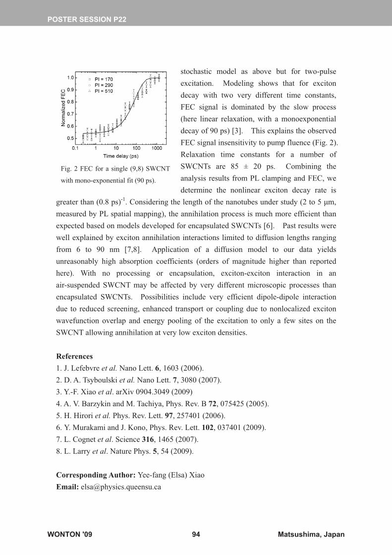
stochastic model as above but for two-pulse excitation. Modeling shows that for exciton decay with two very different time constants, FEC signal is dominated by the slow process (here linear relaxation, with a monoexponential decay of 90 ps) [3]. This explains the observed FEC signal insensitivity to pump fluence (Fig. 2). Relaxation time constants for a number of SWCNTs are 85 ± 20 ps. Combining the analysis results from PL clamping and FEC, we determine the nonlinear exciton decay rate is
greater than (0.8 ps)-1. Considering the length of the nanotubes under study (2 to 5 �m, measured by PL spatial mapping), the annihilation process is much more efficient than expected based on models developed for encapsulated SWCNTs [6]. Past results were well explained by exciton annihilation interactions limited to diffusion lengths ranging from 6 to 90 nm [7,8]. Application of a diffusion model to our data yields unreasonably high absorption coefficients (orders of magnitude higher than reported here). With no processing or encapsulation, exciton-exciton interaction in an air-suspended SWCNT may be affected by very different microscopic processes than encapsulated SWCNTs. Possibilities include very efficient dipole-dipole interaction due to reduced screening, enhanced transport or coupling due to nonlocalized exciton wavefunction overlap and energy pooling of the excitation to only a few sites on the SWCNT allowing annihilation at very low exciton densities.
Fig. 2 FEC for a single (9,8) SWCNT
with mono-exponential fit (90 ps).
References
1. J. Lefebvre et al. Nano Lett. 6, 1603 (2006). 2. D. A. Tsyboulski et al. Nano Lett. 7, 3080 (2007). 3. Y.-F. Xiao et al. arXiv 0904.3049 (2009) 4. A. V. Barzykin and M. Tachiya, Phys. Rev. B 72, 075425 (2005). 5. H. Hirori et al. Phys. Rev. Lett. 97, 257401 (2006). 6. Y. Murakami and J. Kono, Phys. Rev. Lett. 102, 037401 (2009). 7. L. Cognet et al. Science 316, 1465 (2007). 8. L. Larry et al. Nature Phys. 5, 54 (2009). Corresponding Author: Yee-fang (Elsa) Xiao Email: [email protected]
POSTER SESSION P22
WONTON '09 94 Matsushima, Japan
Symmetry-Induced Exciton Distribution between the Bright and Dark States in Single Carbon Nanotubes
Ryusuke Matsunaga1, Kazunari Matsuda1, and Yoshihiko Kanemitsu1,2
1Institute for Chemical Research, Kyoto University, Uji, Kyoto 611-0011, Japan 2Photonics and Electronics Science and Engineering Center, Kyoto University, Kyoto
615-8510, Japan
Although many experimental efforts have been devoted to understanding the
optical properties of semiconducting single-walled carbon nanotubes, exciton dynamics
and distribution between the exciton fine structures remain unclear. The difficulty arises
in both the extrinsic non-radiative decay depending on sample preparations and their
multiple exciton states originating from degenerated band structures. Therefore direct
information on the optically-forbidden (dark) exciton states is needed to elucidate the
intrinsic exciton dynamics.
We have performed photoluminescence (PL) spectroscopy under magnetic
fields for as-grown single carbon nanotubes suspended over grooves [1]. Sharp PL
spectra of single carbon nanotubes enable us to observe the dark excitons due to the
Aharonov-Bohm (AB) effects. The magnetic- and temperature-dependence of the bright
and dark exciton PL spectra revealed that the phonon-induced exciton scattering rate
from the bright to the dark state is only one order of magnitude larger than the dark
exciton recombination rate below 10 K at zero fields [2]. Our results indicate that
excitons are nonequilibriumly distributed between the two states due to the different
parities of their wave functions [3] and that the AB flux enhances the phonon-induced
exciton scattering between these two states. Moreover, our conclusion provides a new
insight concerning the non-zero PL intensities at very low temperatures that have been
recognized as brightening of the dark excitons induced by defects.
References
[1] R. Matsunaga, K. Matsuda, and Y. Kanemitsu, Phys. Rev. Lett. 101, 147404 (2008).
[2] R. Matsunaga, K. Matsuda, and Y. Kanemitsu, submitted (2009).
[3] V. Perebeinos, J. Tersoff, and Ph. Avouris, Nano Lett. 5, 2495 (2005).
Corresponding Author: Ryusuke Matsunaga
Email: [email protected]
POSTER SESSION P23
WONTON '09 95 Matsushima, Japan
Exciton Dynamics in Carbon Nanotubes and Nonlinear Dependence of Photoluminescence Intensity on Pump Power
Maria Hilczer1 and M. Tachiya2
1Institute of Applied Radiation Chemistry, Technical University of Lodz,
Wroblewskiego 15, 93-590 Lodz, Poland 2National Institute of Advanced Industrial Science and Technology (AIST),
ATST Tsukuba Central 5, Tsukuba, Ibaraki 305-8565, Japan
After the discovery of exciton fluorescence from single-walled carbon nanotubes
(SWNT), considerable effort has been devoted to measurements of exciton dynamics in SWNT [1]. The number of excitons produced in a SWNT by photoexcitation is usually very small. Therefore, when one analyzes exciton dynamics in SWNT, one cannot use the conventional deterministic approach which describes exciton decay kinetics by using only the average number of excitons in a SWNT. Instead one has to use a stochastic approach which properly takes into account that the number of excitons in a SWNT is distributed. In the stochastic approach exciton decay kinetics is schematically described by
1nn
n NTNT �����
� �1n
1nn21
n NTNT A
�
������ ��
where NTn stands for a SWNT with n excitons. � is the total unimolecular decay constant of an exciton. �A is the Auger recombination rate constant in a SWNT which contains two excitons. On the basis of the above model we have derived an analytical expression for the average number � �tn of excitons in a SWNT and explained the experimentally observed fluorescence decay kinetics in SWNT [2]. Recently several groups have measured fluorescence intensity from SWNT as a function of pump power and found a nonlinear dependence [3-5]. The fluorescence intensity is given in terms of the average number of excitons in a SWNT
� � � �dttnr�0�����
POSTER SESSION P24
WONTON '09 96 Matsushima, Japan
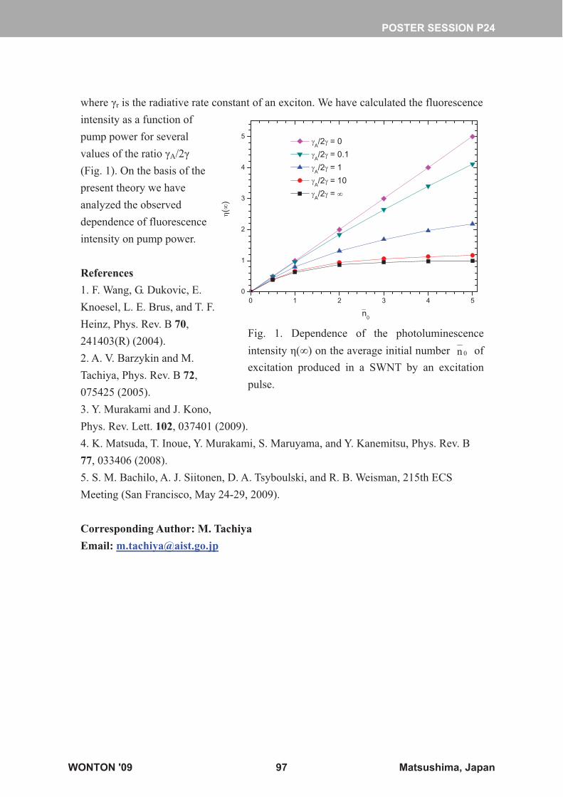
where �r is the radiative rate constant of an exciton. We have calculated the fluorescence intensity as a function of
0 1 2 3 4 50
1
2
3
4
5pump power for several �A/2� = 0
values of the ratio �A/2� �A/2� = 0.1
(Fig. 1). On the basis of the �A/2� = 1
�A/2� = 10
present theory we have �
A/2� = �
analyzed the observed
�(�
)
�n0
dependence of fluorescence intensity on pump power. References
1. F. Wang, G. Dukovic, E. Knoesel, L. E. Brus, and T. F. Heinz, Phys. Rev. B 70, 241403(R) (2004). 2. A. V. Barzykin and M. Tachiya, Phys. Rev. B 72,
Fig. 1. Dependence of the photoluminescenceintensity �( ) on the average initial number 0n ofexcitation produced in a SWNT by an excitation pulse.
075425 (2005). 3. Y. Murakami and J. Kono, Phys. Rev. Lett. 102, 037401 (2009). 4. K. Matsuda, T. Inoue, Y. Murakami, S. Maruyama, and Y. Kanemitsu, Phys. Rev. B 77, 033406 (2008). 5. S. M. Bachilo, A. J. Siitonen, D. A. Tsyboulski, and R. B. Weisman, 215th ECS Meeting (San Francisco, May 24-29, 2009). Corresponding Author: M. Tachiya Email: [email protected]
POSTER SESSION P24
WONTON '09 97 Matsushima, Japan
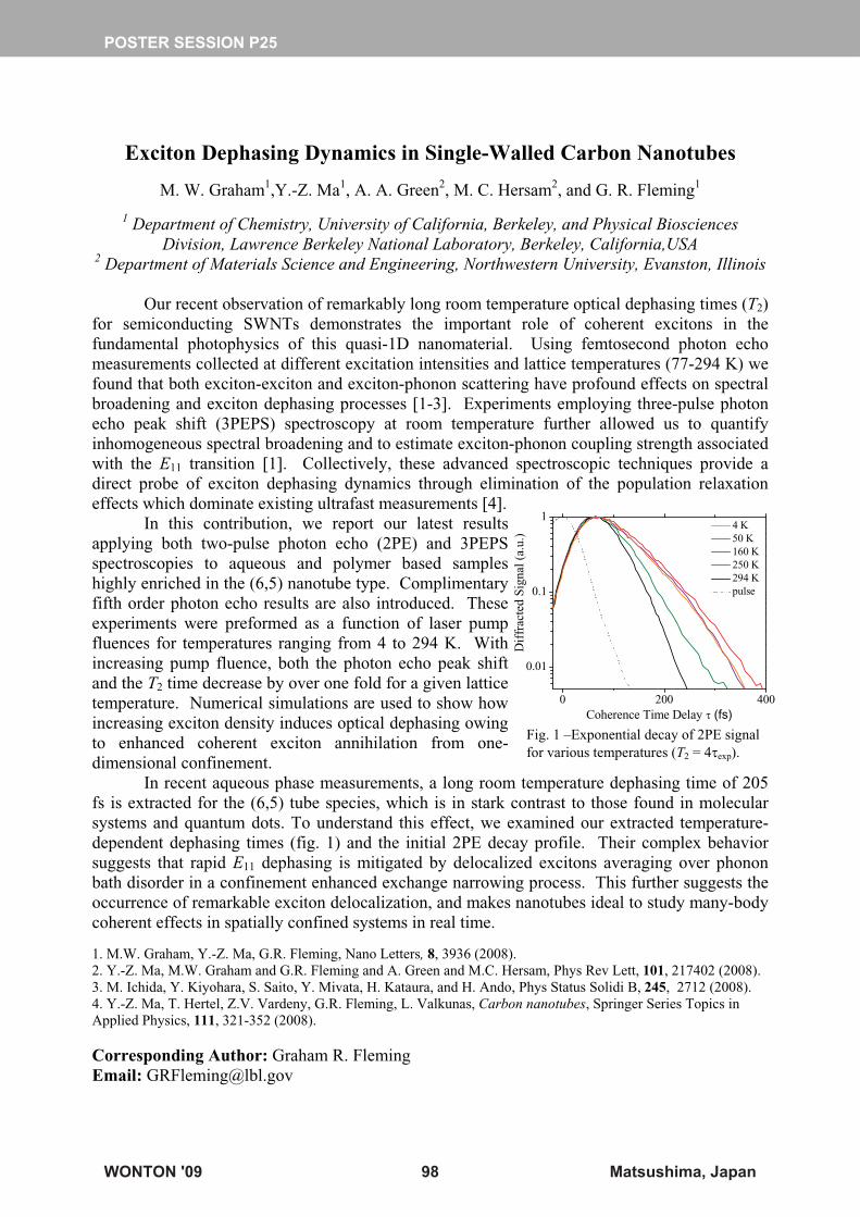
Exciton Dephasing Dynamics in Single-Walled Carbon Nanotubes
M. W. Graham1,Y.-Z. Ma1, A. A. Green2, M. C. Hersam2, and G. R. Fleming1
1 Department of Chemistry, University of California, Berkeley, and Physical Biosciences Division, Lawrence Berkeley National Laboratory, Berkeley, California,USA
2 Department of Materials Science and Engineering, Northwestern University, Evanston, Illinois
0 200 400
0.01
0.1
1
Our recent observation of remarkably long room temperature optical dephasing times (T2)for semiconducting SWNTs demonstrates the important role of coherent excitons in the fundamental photophysics of this quasi-1D nanomaterial. Using femtosecond photon echo measurements collected at different excitation intensities and lattice temperatures (77-294 K) we found that both exciton-exciton and exciton-phonon scattering have profound effects on spectral broadening and exciton dephasing processes [1-3]. Experiments employing three-pulse photon echo peak shift (3PEPS) spectroscopy at room temperature further allowed us to quantify inhomogeneous spectral broadening and to estimate exciton-phonon coupling strength associated with the E11 transition [1]. Collectively, these advanced spectroscopic techniques provide a direct probe of exciton dephasing dynamics through elimination of the population relaxation effects which dominate existing ultrafast measurements [4].
Dif
frac
ted
Sign
al (
a.u.
)In this contribution, we report our latest results
applying both two-pulse photon echo (2PE) and 3PEPS spectroscopies to aqueous and polymer based samples highly enriched in the (6,5) nanotube type. Complimentary fifth order photon echo results are also introduced. These experiments were preformed as a function of laser pump fluences for temperatures ranging from 4 to 294 K. With increasing pump fluence, both the photon echo peak shift and the T2 time decrease by over one fold for a given lattice temperature. Numerical simulations are used to show how increasing exciton density induces optical dephasing owing to enhanced coherent exciton annihilation from one-dimensional confinement.
Coherence Time Delay � (fs)
4 K 50 K 160 K 250 K 294 K pulse
Fig. 1 –Exponential decay of 2PE signal for various temperatures (T2 = 4�exp).
In recent aqueous phase measurements, a long room temperature dephasing time of 205 fs is extracted for the (6,5) tube species, which is in stark contrast to those found in molecular systems and quantum dots. To understand this effect, we examined our extracted temperature-dependent dephasing times (fig. 1) and the initial 2PE decay profile. Their complex behavior suggests that rapid E11 dephasing is mitigated by delocalized excitons averaging over phonon bath disorder in a confinement enhanced exchange narrowing process. This further suggests the occurrence of remarkable exciton delocalization, and makes nanotubes ideal to study many-body coherent effects in spatially confined systems in real time.
1. M.W. Graham, Y.-Z. Ma, G.R. Fleming, Nano Letters, 8, 3936 (2008). 2. Y.-Z. Ma, M.W. Graham and G.R. Fleming and A. Green and M.C. Hersam, Phys Rev Lett, 101, 217402 (2008). 3. M. Ichida, Y. Kiyohara, S. Saito, Y. Mivata, H. Kataura, and H. Ando, Phys Status Solidi B, 245, 2712 (2008). 4. Y.-Z. Ma, T. Hertel, Z.V. Vardeny, G.R. Fleming, L. Valkunas, Carbon nanotubes, Springer Series Topics in Applied Physics, 111, 321-352 (2008).
Corresponding Author: Graham R. Fleming Email: [email protected]
POSTER SESSION P25
WONTON '09 98 Matsushima, Japan
Exciton Radiative Lifetimes and Coherence Lengths in Single-Walled Carbon Nanotubes
Yuhei Miyauchi1, Ryusuke Matsunaga1, Hideki Hirori2, Kazunari Matsuda1,
and Yoshihiko Kanemitsu1
1Institute for Chemical Research, Kyoto University, Gokasho, Uji, Kyoto 611-0011, Japan
2Institute for Integrated Cell-Material Sciences, Kyoto University, Sakyo-ku, Kyoto 606-8502, Japan
We have studied the radiative lifetimes of one-dimensional excitons in single-walled carbon nanotubes (SWNTs) from simultaneous measurements of the photoluminescence (PL) lifetimes [1] and the PL quantum yields. A high-quality sample of PFO [poly(9,9-dioctylfluorenyl-2,7-diyl)] dispersed-SWNTs [2] was used for the optical measurements. The PL lifetimes and the PL quantum yields were ~40-60 ps and ~1.5% for small diameter (<1nm) SWNTs, respectively. The evaluated radiative lifetimes were ~3-4 ns for SWNTs with diameters ~0.8-1.0 nm at room temperature. For SWNTs with diameters more than 1 nm, the radiative lifetimes slightly increased with the tube diameter. The exciton spatial coherence lengths were of the order of 10 nm along the tube axis at room temperature, as deduced from the radiative lifetimes. Furthermore, we discuss the dynamics of bright and dark excitons [3] from the temperature dependence of the radiative lifetimes. References [1] H. Hirori, K. Matsuda, Y. Miyauchi, S. Maruyama, and Y. Kanemitsu, Phys. Rev. Lett. 97, 257401 (2006). [2] A. Nish, J.-Y. Hwang, J. Doig, and R. J. Nicholas, Nat. Nanotechnol. 22, 640 (2007). [3] R. Matsunaga, K. Matsuda, and Y. Kanemitsu, Phys. Rev. Lett. 1101, 147404 (2008). Corresponding Author: Yuhei Miyauchi Email:[email protected]
POSTER SESSION P26
WONTON '09 99 Matsushima, Japan
Excitons in carbon nanotubewithin effective-mass approximation
Tsuneya ANDO1 and Seiji URYU2
1Department of Physics, Tokyo Institute of Technology2-12-1 Ookayama, Meguro-ku, Tokyo 152-8551, Japan
2Department of Materials Science and Engineering, Iwate University4–3–5 Ueda, Morioka 020-8551, Japan
A carbon nanotube is composed of concentric tubes of rolled two-dimensional graphite sheets,on which hexagons are arranged in a helical fashion about the axis. Since the first discovery quitea number of studies have been reported on their electronic properties because of their uniquetopological structures. The purpose of this talk is to give a brief review on recent theoretical in-vestigations on optical properties of carbon nanotubes in the presence of Aharonov-Bohm magneticflux (see a recent review [1, 2] and references cited therein).
The topics include an effective-mass description of electronic states and close relationship withneutrino physics, interaction effects on the band structure [3, 4], optical absorption for parallelpolarization and strong exciton effect [5, 6], the Aharonov-Bohm (AB) splitting observed recently[7, 8], dark and bright excitons due to the short-range part of the Coulomb interaction causingmixing between K and K’ points, and their ordering and relative energy splitting and strong effectsof AB flux [9], and two-phonon absorption due to exciton excited states [10]. Without excitoneffects, there are no peaks in absorption spectra of light polarized perpendicularly to a tube axisbecause of strong depolarization effect [11]. However, the strong exciton effect causes absorptionpeaks for perpendicular light though its intensity is reduced in comparison with that for parallellight [12], as experimentally observed recently [13, 14]. The exciton effect is important also inmetallic carbon nanotubes [15]. The family effect can also be understood, in particular for thefirst semiconducting gap, mostly by considering trigonal warping described by a higher-oder k·pterm [16], and by the curvature and associated lattice distortion described by effective magneticflux [17].
References[1] T. Ando, J. Phys. Soc. Jpn. 74, 777 (2005).[2] T. Ando and S. Uryu, Phys. Stat. Sol. C 6, 173 (2008).[3] H. Sakai, H. Suzuura, and T. Ando, J. Phys. Soc. Jpn. 72, 1698 (2003).[4] H. Sakai, H. Suzuura, and T. Ando, Physica E 22, 704 (2004).[5] T. Ando, J. Phys. Soc. Jpn. 66, 1066 (1997).[6] T. Ando, J. Phys. Soc. Jpn. 73, 3351 (2004).[7] S. Zaric, G. N. Ostojic, J. Kono, J. Shaver, V. C. Moore, M. S. Strano, R. H. Hauge, R. E.
Smalley, and X. Wei, Science 304, 1129 (2004).[8] H. Yokoi, N. Kuroda, Y. Kim, N. Minami, S. Kazaoui, K. Uchida, and S. Takeyama, in Narrow
Gap Semiconductors 2005 (Institute of Physics Conference Series Number 187) edited by J.Kono and J. Leotin, (Taylor & Francis, London, 2006), p. 278.
[9] T. Ando, J. Phys. Soc. Jpn. 75, 024707 (2006).[10] S. Uryu, H. Ajiki, and T. Ando, Phys. Rev. B 77, 115414 (2008).[11] H. Ajiki and T. Ando, Physica B 201, 349 (1994); Jpn. J. Appl. Phys. Suppl. 34-1, 107
(1995).[12] S. Uryu and T. Ando, Phys. Rev. B 74, 155411 (2006).[13] Y. Miyauchi, M. Oba, and S. Maruyama, Phys. Rev. B 74, 205440 (2006).[14] J. Lefebvre and P. Finnie, Phys. Rev. Lett. 98, 167406 (2007).[15] S. Uryu and T. Ando, Phys. Rev. B 77, 205407 (2008).[16] H. Ajiki and T. Ando, J. Phys. Soc. Jpn. 65, 505 (1996).[17] H. Suzuura and T. Ando, Phys. Rev. B 65, 235412 (2002).
POSTER SESSION P27
WONTON '09 100 Matsushima, Japan

&�����'������( ) �#�������������������)� ����������*��������#��&�"�� ���
�$��!������'���"� ����G����
#���� �� ��!��(��&�?������*$&�$��� �� (� ��@�2������2��, ��$�& �����������
B��$�5������C��B��$3���� $�� �7�735��5��E$�$��
5� ���������� ����$������� ���� 8���9��#�� ��� ������� � ����������$ �:�: ��� ���������� �$�&�� ��$$�� �������$��� ���������� ���� ���� ��������������� ��� =�>:!��#����%��������%�$��� 7���������� ��$��� ��� ����$�&�� �� ������#�������#���� %�$�������:� ���7��" 7���#��&������$$�� ��$������� %�� � �����&�� ������������ �����7� �� ���$$�� �#�����������&��� ��:%������$%��7 �� � ���#����% ��������$�&�� �� ������� ���%������ %��� ��������7����%��#����$�� �����%�� �#�8����� 9����� �#�8���"9�&�� ��������� :%�� ���&�� �� � ������ ���$����� ��� ��(�#����%�������� ��(##����% 8(� (#�(�� (�9 ���&��������% � #
�
GB B 7���� ��� #� #� """�� G �� ��
�� ����$�����7�#������ ��%������ � � � # � # � #
, , ,� L BB B B� �� �
� � � ������� ����� ��� ����
,� �
GL
� � �
G$ 8� �������� � ��$((��(�(��&�� ��9 # �
GL ��
# �
G$ 8����� �� � ������� � � �� �$ ((� �� (�( �&�� ��9 ��� ���" � �������� �$ ������ % ��� ����: !�� ������� �$ � ���� ����� ������ % ��#�� ���� ���&�� �� 7�� ((<(�(� �� ((�<(�( �&�� �� ��� � �� � ���#����% ���� ����� ������ 7�� �� (�� (�#����%�:)�� ����� 7��� $���G��� ���� ����� 7����#�����&�� �� � �������7�@��:�:!�����#���� 7������ � $�� �48�9!�� ����� �� � ������� � � �� � ��� ����� ������ ��% ���������: 8��9 �
,� L ���
������� ��% � #� �
GL �� ## �
GL 7� � ,G � : !�� $����� ���� � �% ���"� �$
� ������� �&�� � � � �� � ������ ������ ��� ����������$������������ %:!���� ����������� ���%���"��$#��&�� �� $�� �� 7��" ������ % �� � ����� ����� ���� ��&�� �� ���� �� � �����������$���� ��:�����������:!:)�� -:'�%�:���:-�:�� BBB8#,,+9:�������"��� �#�$�������+������ ���� ������ �,��#.��/��� .��.0"�
Eb22p(Q)
Ea22p(Q)
Eb21s(Q)
Ea21s(Q)
Eb12p(Q)
Ea12p(Q)
Eb11s(Q)
Ea11s(Q)
�@��:������� ����$����%��#����$���#��&�� �������������G��� ���� ����%
������ %��� ����:
POSTER SESSION P28
WONTON '09 101 Matsushima, Japan
Theory of 1D Exciton and its Application to SWNT
Seiji Sakoda and Madoka Tokumoto
Department of Applied Physics, National Defense Academy, 1-10-20 Hashirimizu, Yokosuka, Kanagawa 239-8686, Japan
Motivations We shall reinvestigate the earlier results [1,2] for one dimensional excitons from the viewpoint of quantum mechanics of singular potentials [3,4]. Results We show that the binding energy of the one dimensional exciton remains finite even in the limit of the bare Coulomb potential. In the same limit, wavefunctions of the continuum spectrum with even parity(direct allowed transitions) will not vanish at the origin, but result in non-zero, though suppressed, Sommerfeld factors. We require that we should be able to find a plane wave of the free particle when we switch off the Coulomb interaction, while the one in Ref’s [1] and [2] imposes non-trivial boundary condition at the origin. This difference in boundary conditions at the singularity results in different spectrum of exciton states with even parity in addition to the ordinary hydrogen-like spectrum for states with odd parity(Fig. 1). Since even and odd parity states are determined by the poles of the di-Gamma function and the Gamma function, respectively, they appear in an alternate manner. We have made an analysis of the experimental result of Ref. [5] by use of this new exciton spectrum and found that the dielectric constant of SWNT should be about 1.6 times larger than that of Ref. [5]. References 1. R. Loudon, Am. J. Phys. 27, 649(1959), R. J. Elliott and R. Loudon, J. Phys. Chem. Solids 15, 196(1960).
2. T. Ogawa and T. Takagahara, Phys. Rev. B 43, 14 325(1991),T. Ogawa and T. Takagahara, Phys. Rev. B 44, 8138(1991)
3. I. Tsutsui, T. Fülöp and T. Cheon, J. Phys. A: Math. Gen. 36, 275-287(2003)
4. S. Sakoda, Mod. Phys. Lett. A 23, 3057-3076(2008)
5. F. Wang, G. Dukovic, L. E. Brus, and T. F. Heinz, Science 308, 838-841 (2005)
POSTER SESSION P29
WONTON '09 102 Matsushima, Japan
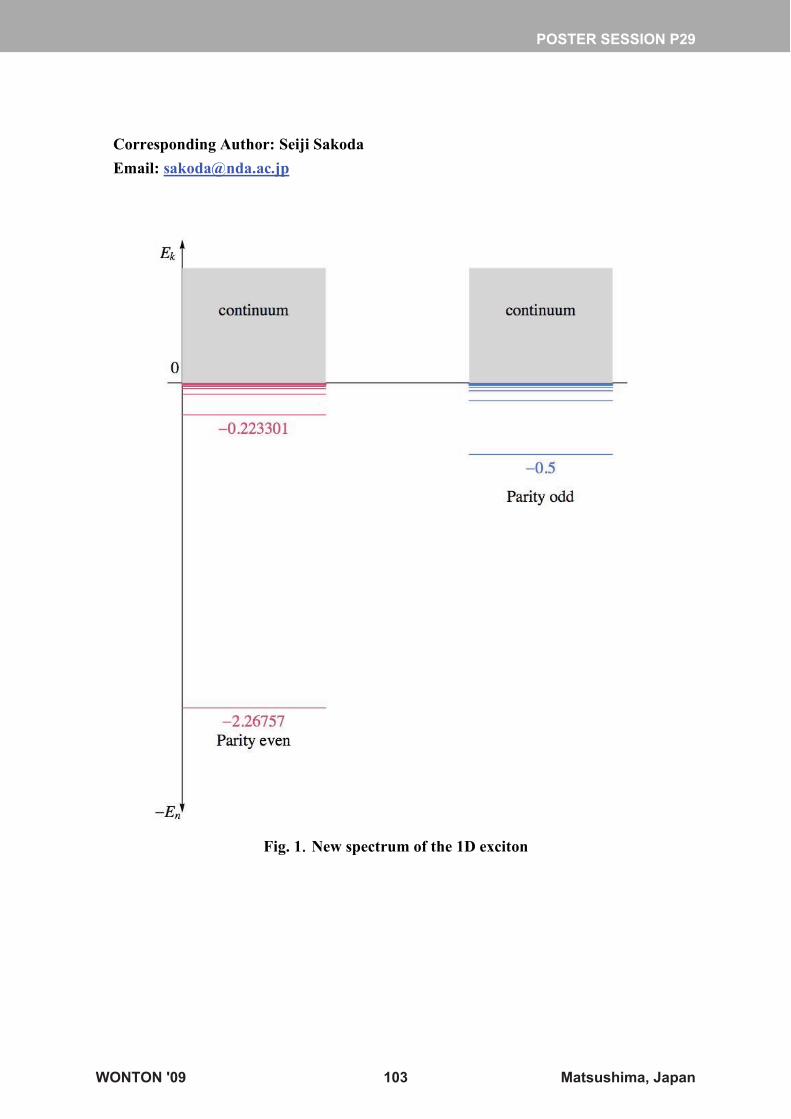
Corresponding Author: Seiji Sakoda Email: [email protected]
Fig. 1.. New spectrum of the 1D exciton
POSTER SESSION P29
WONTON '09 103 Matsushima, Japan
Reflectance spectra of individual metallic single walled carbon nanotubes.
Hualing Zeng,1 Hongbo Zhao,1,2 Fu-Chun Zhang,1, 2 and Xiaodong Cui1
1 Department of Physics, The University of Hong Kong, Hong Kong, China
2 Center of Theoretical and Computational Physics, The University of Hong Kong, Hong
Kong, China
Abstract:
Due to the reduced dimensionality, single-walled carbon nanotubes show strong
Coulomb interaction and enhanced electron-phonon interactions. Experimental evidence
for both phenomenon in the individual nanotube level is few. We report reflection
experiment of an individual single-walled carbon nanotube that shows both.[1] Individual
(13,10) metallic nanotube is fabricated cross a slit, focused laser light from near-infrared
to visible shine on the nanotube and reflection spectrum is collected. The lower energy
part of the spectrum features two well defined peaks separated by 0.2eV. We show that
while the lower peak is from the lowest exciton, the higher peak could be the phonon side
band of exciton, a result of strong electron-phonon coupling. Our calculation also gives
estimation of static dielectric constant.[2]
References:
[1]. HL Zeng, LY Jiao, XJ Xian, XC Qin, ZF Liu, and XD Cui, (Nanotechnology Vol19
(2008) 045708)
[2]. HL Zeng, HB Zhao, FC Zhang, and XD Cui, (To appear in Physical Review Letters)
POSTER SESSION P30
WONTON '09 104 Matsushima, Japan
Magneto-optical Spectroscopy of Metallic Single-Walled Carbon Nanotubes
Thomas A. Searles1, Junichiro Kono1, Yasutaka Imanaka2,
Jeffery A. Fagan3, and Erik K. Hobbie3
1 Department of Electrical and Computer Engineering, Rice University, Houston,
Texas 77005, U.S.A. 2 National Institute of Materials Science, 3-13 Sakura, Tsukuba, Ibaraki 305-0003, Japan
3 Polymer Division, National Institute of Standards and Technology, Gaithersburg,
Maryland 20899, U.S.A.
Through polarization-dependent magneto-absorption spectroscopy, we have extracted the
magnetic susceptibility anisotropy for metallic carbon nanotubes and compared it with
that of semiconducting carbon nanotubes for the first time. The magnetic properties of
carbon nanotubes (both metallic and semiconducting species) change with the direction
of the magnetic field with respect to the tube axis, yielding a magnetic anisotropy given
by �� = �// – �. Metallic nanotubes are paramagnetic along the tube axis (�// > 0) and
diamagnetic in the perpendicular direction (� < 0), whereas semiconducting tubes are
diamagnetic in all directions (�//, � < 0) [1]. This anisotropy of magnetic susceptibilities
results in the nanotubes in solution aligning as the magnetic field is increased. This,
combined with the anisotropic optical absorption properties of carbon nanotubes, allows
for the use of polarization-dependent optical absorption to measure the degree of
magnetic alignment through magnetic linear dichroism (MLD) spectroscopy. Previous
MLD studies on HiPco semiconducting nanotubes found that �� � 1.4 ¡ 105 emu/mol,
but there was no information on �� for metallic nanotubes [2,3].
Our measurements on length-sorted, (6,5)-enriched CoMoCAT single-walled carbon
nanotubes were made using the 35 T Hybrid Magnet in the High Magnetic Field Facility
of the National Institute of Materials Science in Tsukuba, Japan. We measured
absorption with light polarization both perpendicular and parallel to the magnetic field as
seen in Fig. 1, to determine the MLD. By relating these values with the nematic order
parameter for alignment S (Fig. 2), we found that the (6,6) nanotube aligns more rapidly
with the magnetic field than semiconducting nanotubes [specifically the (6,5) tube].
POSTER SESSION P31
WONTON '09 105 Matsushima, Japan
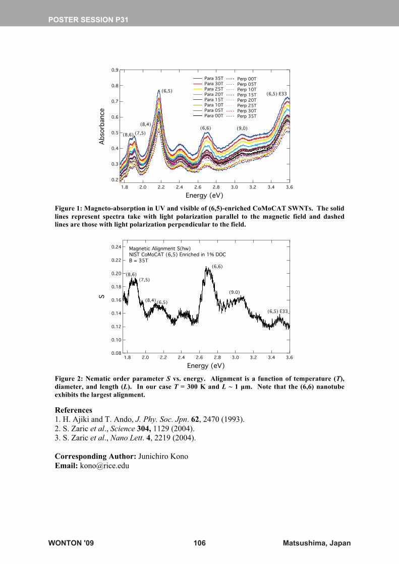
Figure 1: Magneto-absorption in UV and visible of (6,5)-enriched CoMoCAT SWNTs. The solid lines represent spectra take with light polarization parallel to the magnetic field and dashed lines are those with light polarization perpendicular to the field.
Figure 2: Nematic order parameter S vs. energy. Alignment is a function of temperature (T), diameter, and length (L). In our case T = 300 K and L ~ 1 μm. Note that the (6,6) nanotube exhibits the largest alignment.
References 1. H. Ajiki and T. Ando, J. Phy. Soc. Jpn. 62, 2470 (1993). 2. S. Zaric et al., Science 304, 1129 (2004). 3. S. Zaric et al., Nano Lett. 4, 2219 (2004).
Corresponding Author: Junichiro Kono Email: [email protected]
POSTER SESSION P31
WONTON '09 106 Matsushima, Japan
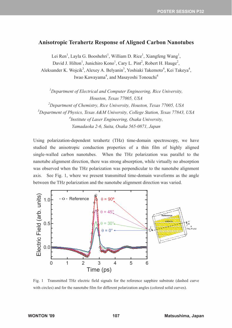
Anisotropic Terahertz Response of Aligned Carbon Nanotubes
Lei Ren1, Layla G. Booshehri1, William D. Rice1, Xiangfeng Wang1, David J. Hilton1, Junichiro Kono1, Cary L. Pint2, Robert H. Hauge2,
Aleksander K. Wojcik3, Alexey A. Belyanin3, Yoshiaki Takemoto4, Kei Takeya4, Iwao Kawayama4, and Masayoshi Tonouchi4
1Department of Electrical and Computer Engineering, Rice University,
Houston, Texas 77005, USA 2Department of Chemistry, Rice University, Houston, Texas 77005, USA
3Department of Physics, Texas A&M University, College Station, Texas 77843, USA 4Institute of Laser Engineering, Osaka University,
Yamadaoka 2-6, Suita, Osaka 565-0871, Japan
Using polarization-dependent terahertz (THz) time-domain spectroscopy, we have studied the anisotropic conduction properties of a thin film of highly aligned single-walled carbon nanotubes. When the THz polarization was parallel to the nanotube alignment direction, there was strong absorption, while virtually no absorption was observed when the THz polarization was perpendicular to the nanotube alignment axis. See Fig. 1, where we present transmitted time-domain waveforms as the angle between the THz polarization and the nanotube alignment direction was varied.
�
�
1.0
0.5
0.0
Ele
ctric
Fie
ld (
arb.
uni
ts)
6543210Time (ps)
��= 90º
� = 45°
� = 30°
� = 0°
Reference
Reference
Fig. 1 Transmitted THz electric field signals for the reference sapphire substrate (dashed curve
with circles) and for the nanotube film for different polarization angles (colored solid curves).
POSTER SESSION P32
WONTON '09 107 Matsushima, Japan
The sample was synthesized via chemical vapor deposition and transferred onto a sapphire substrate through a high temperature water etching process [1]. Experimental details are described elsewhere [2]. Through a proper model, the THz complex dynamic conductivity of the SWNTs was extracted and showed a non-Drude-like frequency dependence, with the real part monotonically increasing with increasing frequency. The degree of polarization in terms of absorbance was calculated to be 1, and the reduced linear dichroism was calculated to be 3 using the theory of linear dichroism for an ensemble of anisotropic molecules, which demonstrates the nematic order parameter of the SWNTs in the film to be 1. This indicates that the alignment of the nanotubes is perfect and any misalignment must have characteristic length scales much smaller than the wavelengths used in these experiments (1.5 mm – 150 �m). All these findings suggest that this type of aligned single-walled carbon nanotube film performs as an ideal linear polarizer in the THz frequency range. References
1. C. L. Pint, Y.-Q. Xu, M. Pasquali, and R. H. Hauge, ACS Nano 2, 1871 (2008). 2. L. Ren et al., arXiv:0903.2583v1.
Corresponding Author: Junichiro Kono Email: [email protected]
POSTER SESSION P32
WONTON '09 108 Matsushima, Japan
Finite-length effects on optical absorptionin metallic carbon nanotubes
Takeshi NAKANISHI1 and Tsuneya ANDO2
1Nanotube Research Center, AIST1–1–1 Higashi, Tsukuba 305-8565, Japan
2Department of Physics, Tokyo Institute of Technology2–12–1 Ookayama, Meguro-ku, Tokyo 152-8551, Japan
Carbon nanotubes are a one-dimensional conductor consisting of rolled graphene sheets. Re-cently, cutting and length selection of single-wall carbon nanotubes have been studied [1-3]. Opticalabsorption in low-frequency region was recently reported in such nanotubes [4-6]. In short carbonnanotubes with good conductivity, depolarization field in the axis direction becomes importantdue to the accumulated charge at both ends of nanotubes in optical absorption [7]. The purposeof this paper is to calculate a low-frequency optical response in metallic carbon nanotubes withfinite length.
We consider a metallic carbon nanotube with finite length l under an external electric field inthe axis direction. We solve the electrostatic equations instead of full Maxwell’s equation, which isjustified by the fact that the plasmon velocity in carbon nanotubes is much smaller than the lightvelocity. The response of the system can generally be described by a nonlocal conductivity. Weconsider the case that the length of the nanotube is much larger than the mean free path. Thus, wecan neglect effects of edges on the conductivity and use the Boltzmann conductivity in infinitelylong nanotubes, employing a relaxation-time approximation. In actual numerical calculations, weconsider a periodic array of the nanotubes and calculate an effective electric field including effectsof polarization charges.
Calculated power absorption oscillates with decreasing∼ω−2 in the low frequency region. Thefrequency of the peaks is inversely proportional to the length of nanotubes. Calculated powerabsorption is compared with that in a single-mode approximation in which a resonance occurs atfrequency ω=vQQn with Qn≈(2n+1)π/l (n=0, 1, · · ·), where vQ is a plasmon velocity and a fewtimes larger than the Fermi velocity in carbon nanotubes. We find that the calculated peaks areshifted significantly from those in the single-mode estimation, except for the main peak (n = 0).Actually, the electric field shows significant mixture of other modes, which are involved to formthe induced electric field at the both ends of the nanotubes.
References[1] K. J. Ziegler, D. J. Schmidt, U. Rauwald, K. N. Shah, E. L. Flor, R. H. Hauge, and R. E.
Smalley: Nano Lett. 5, 2355 (2005).[2] F. Hennrich, R. Krupke, K. Arnold, J. A. Rojas Stu1tz, S. Lebedkin, T. Koch, T. Schimmel,
and M. M. Kappes: J. Phys. Chem. B 111, 1932 (2007).[3] J. A. Fagan, M. L. Becker, J. Chun and E. K. Hobbie: Adv. Mater. 20, 1609 (2008).[4] M. E. Itkis, S. Niyogi, M. E. Meng, M. A. Hamon, H. Hu, and R. C. Haddon: Nano Lett. 2,
155 (2002).[5] N. Akima, Y. Iwasa, S. Brown, A. M. Barbour, J. Cao, J. L. Musfeldt, H. Matsui, N. Toyota,
M. Shiraishi, H. Shimoda, and O. Zhou: Adv. Mater. 18, 1166 (2006).[6] T. Kampfrath, K. von Volkmann, C. M. Aguirre, P. Desjardins, R. Martel, M. Krenz, C.
Frischkorn, M. Wolf, and L. Perfetti: Phys. Rev. Lett. 101, 267403 (2008).[7] G. Ya. Slepyan, M. V. Shuba, S. A. Maksimenko, and A. Lakhtakia: Phys. Rev. B 73, 195416
(2006).
POSTER SESSION P33
WONTON '09 109 Matsushima, Japan
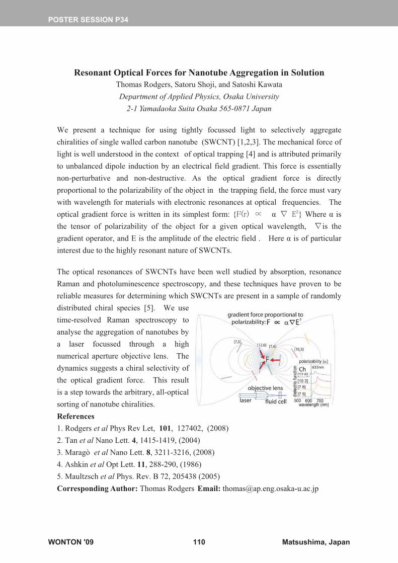
Resonant Optical Forces for Nanotube Aggregation in Solution Thomas Rodgers, Satoru Shoji, and Satoshi Kawata Department of Applied Physics, Osaka University
2-1 Yamadaoka Suita Osaka 565-0871 Japan
We present�a technique for using tightly focussed light to selectively� aggregate chiralities of single walled carbon nanotube�(SWCNT) [1,2,3]. The mechanical force of light is well understood in the context� of optical trapping [4] and is attributed primarily to unbalanced dipole induction by an electrical field gradient. This force is essentially non-perturbative and non-destructive. As the optical gradient force is directly proportional to the polarizability of the object in� the trapping field, the force must vary with wavelength for materials with electronic resonances at optical� frequencies.��The optical gradient force is written in its simplest form: {����� �� £�����} Where £ is the tensor of polarizability of the object for a given optical wavelength,� �is the gradient operator, and E is the amplitude of the electric field .��Here £ is of particular interest due to the highly resonant nature of SWCNTs.
The optical resonances of SWCNTs have been well studied by absorption, resonance Raman and photoluminescence spectroscopy, and these techniques have proven to be reliable measures for determining which SWCNTs are present in a sample of randomly distributed chiral species�[5].��We use time-resolved Raman spectroscopy to analyse the aggregation of nanotubes by a laser focussed through a high numerical aperture objective lens. The dynamics suggests a chiral selectivity of the optical gradient force. This result is a step towards the arbitrary, all-optical sorting of nanotube chiralities. References 1. Rodgers et al Phys Rev Let,�101,�127402,�(2008) 2. Tan et al Nano Lett. 4, 1415-1419, (2004)��3. Maragò�et al Nano Lett. 8, 3211-3216, (2008) 4. Ashkin et al Opt Lett. 11, 288-290, (1986)��5. Maultzsch et al Phys. Rev. B 72, 205438 (2005) Corresponding Author: Thomas Rodgers Email: [email protected]
POSTER SESSION P34
WONTON '09 110 Matsushima, Japan
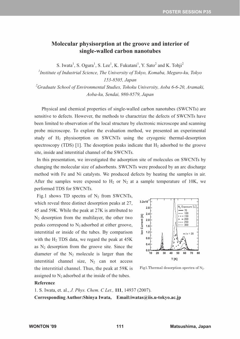
Molecular physisorption at the groove and interior of single-walled carbon nanotubes
S. Iwata1, S. Ogura1, S. Lee1, K. Fukutani1, Y. Sato2 and K. Tohji2
1Institute of Industrial Science, The University of Tokyo, Komaba, Meguro-ku, Tokyo
153-8505, Japan 2Graduate School of Environmental Studies, Tohoku University, Aoba 6-6-20, Aramaki,
Aoba-ku, Sendai, 980-8579, Japan
� Physical and chemical properties of single-walled carbon nanotubes (SWCNTs) are
sensitive to defects. However, the methods to charactrize the defects of SWCNTs have
been limited to observation of the local structure by electronic microscope and scanning
probe microscope. To explore the evaluation method, we presented an experimental
study of H2 physisorption on SWCNTs using the cryogenic thermal-desorption
spectroscopy (TDS) [1]. The desorption peaks indicate that H2 adsorbed to the groove
site, inside and interstitial channel of the SWCNTs.
In this presentation, we investigated the adsorption site of molecules on SWCNTs by
changing the molecular size of adsorbents. SWCNTs were produced by an arc discharge
method with Fe and Ni catalysts. We produced defects by heating the samples in air.
After the samples were exposed to H2 or N2 at a sample temperature of 10K, we
performed TDS for SWCNTs.
Fig.1 shows TD spectra of N2 from SWCNTs,
which reveal three distinct desorption peaks at 27,
45 and 59K. While the peak at 27K is attributed to
N2 desorption from the multilayer, the other two
peaks correspond to N2 adsorbed at either groove,
interstitial or inside of the tubes. By comparison
with the H2 TDS data, we regard the peak at 45K
as N2 desorption from the groove site. Since the
diameter of the N2 molecule is larger than the
interstitial channel size, N2 can not access
the interstitial channel. Thus, the peak at 59K is
3.2x10⁻⁷
2.8
2.4
2.0
1.6
1.2
0.8
0.4
0.0
Ion
Cu
rren
t [A
]
8070605040302010
T [K]
��������
���� ��������
�����������������������������
Fig1.Thermal desorption spectra of N2.
assigned to N2 adsorbed at the inside of the tubes.
Reference
1. S. Iwata, et. al., J. Phys. Chem. C Let., 111, 14937 (2007).
Corresponding Author:Shinya Iwata, Email:[email protected]
POSTER SESSION P35
WONTON '09 111 Matsushima, Japan
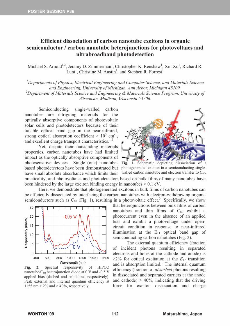
Efficient dissociation of carbon nanotube excitons in organic semiconductor / carbon nanotube heterojunctions for photovoltaics and
ultrabroadband photodetection
Michael S. Arnold1,2, Jeramy D. Zimmerman1, Christopher K. Renshaw1, Xin Xu1, Richard R. Lunt1, Christine M. Austin1, and Stephen R. Forrest1
1Departments of Physics, Electrical Engineering and Computer Science, and Materials Science and Engineering, University of Michigan, Ann Arbor, Michigan 48109.
2Department of Materials Science and Engineering & Materials Science Program, University of Wisconsin, Madison, Wisconsin 53706.
Semiconducting single-walled carbon nanotubes are intriguing materials for the optically absorptive components of photovoltaic solar cells and photodetectors because of their tunable optical band gap in the near-infrared, strong optical absorption coefficient > 105 cm-1,and excellent charge transport characteristics.1,2
Yet, despite their outstanding materials properties, carbon nanotubes have had limited impact as the optically absorptive components of photosensitive devices. Single (one) nanotube-based photodetectors have been demonstrated but have small absolute absorbance which limits their practicality, and photovoltaics and photodetectors based on bulk films of many nanotubes have been hindered by the large exciton binding energy in nanotubes > 0.1 eV.
Here, we demonstrate that photogenerated excitons in bulk films of carbon nanotubes can be efficiently dissociated by interfacing the carbon nanotubes with electron-withdrawing organic semiconductors such as C60 (Fig. 1), resulting in a photovoltaic effect.3 Specifically, we show
that heterojunctions between bulk films of carbon nanotubes and thin films of C60 exhibit a photocurrent even in the absence of an applied bias and exhibit a photovoltage under open-circuit condition in response to near-infrared illumination at the E11 optical band gap of semiconducting carbon nanotubes (Fig. 2).
The external quantum efficiency (fraction of incident photons resulting in separated electrons and holes at the cathode and anode) is >2% for optical excitation at the E11 transition and is absorption limited. The internal quantum efficiency (fraction of absorbed photons resulting in dissociated and separated carriers at the anode and cathode) > 40%, indicating that the driving force for exciton dissociation and charge
Fig. 1. Schematic depicting dissociation of a photogenerated exciton in a semiconducting single-walled carbon nanotube and electron transfer to C60.
Fig. 2. Spectral responsivity of HiPCO nanotube/C60 heterojunction diode at 0 V and -0.5 V applied bias (dashed and solid line, respectively). Peak external and internal quantum efficiency at 1155 nm > 2% and > 40%, respectively.
POSTER SESSION P36
WONTON '09 112 Matsushima, Japan
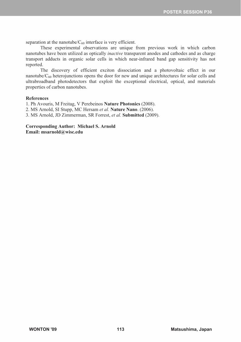
separation at the nanotube/C60 interface is very efficient. These experimental observations are unique from previous work in which carbon
nanotubes have been utilized as optically inactive transparent anodes and cathodes and as charge transport adducts in organic solar cells in which near-infrared band gap sensitivity has not reported.
The discovery of efficient exciton dissociation and a photovoltaic effect in our nanotube/C60 heterojunctions opens the door for new and unique architectures for solar cells and ultrabroadband photodetectors that exploit the exceptional electrical, optical, and materials properties of carbon nanotubes.
References 1. Ph Avouris, M Freitag, V Perebeinos Nature Photonics (2008).2. MS Arnold, SI Stupp, MC Hersam et al. Nature Nano. (2006). 3. MS Arnold, JD Zimmerman, SR Forrest, et al. Submitted (2009).
Corresponding Author: Michael S. Arnold Email: [email protected]
POSTER SESSION P36
WONTON '09 113 Matsushima, Japan

WONTON '09 114 Matsushima, Japan
Author Index
AAchete, Carlos. A. ----------------------- 33 Achiba, Yohji ----------------------------- 63 Ackermann, Thomas -------------------- 21 Aitchison, Brad -------------------------- 79 Ando, Hiroaki ---------------------------- 32 Ando, Tsuneya --------------- 50, 100, 109 Arepalli, Sivaram ------------------------ 69 Arnold, Michael S. -------------------- 112 Asada, Yuki ------------------------------- 73 Asaka, K. ---------------------------------- 57 Asano, Kenichi --------------------------- 50 Austin, Christine M. ------------------- 112
BBauri, Ajoy ------------------------------- 72 Belyanin, Alexey A. ------------------- 107 Booshehri, Layla G. --------------- 86, 107 Brown, David P -------------------------- 79 Burger, Lea ------------------------------- 22
CCancado, Luiz Gustavo ----------------- 40 Capaz, Rodrigo B. ----------------------- 33 Chiashi, Shohei ----------------- 54, 87, 90 Chokan, Tomohito ----------------------- 90 Cognet, Laurent --------------------- 88, 89 Crochet, Jared ---------------------------- 21 Cui, Xiaodong -------------------------- 104
DDensmore, Crystal G. ------------------- 17 Doorn, Stephen K. -------------- 17, 69, 88 Dresselhaus, Mildred S. ------------ 49, 82 Dresselhaus, Gene ----------------------- 82 Duque, Juan G. ---------------------- 88, 89
EEinarsson, Erik ------------------ 74, 76, 78
FFagan, J. A. ----------------------------- 105 Feng, Ye ----------------------------------- 16 Ferrari, Andrea C. ------------------------ 52 Ferreira, Erlon H. M. -------------------- 33 Finnie, Paul ------------------------------- 30 Flahaut, Emmanuel ---------------------- 75 Fleurier, Romain ------------------------- 75 Forrest, Stephen R. -------------------- 112 Fraser, James M. ------------------------- 93 Freitag, M. -------------------------------- 42 Fujii, Shunjiro ---------------------------- 16 Fukutani, K. ----------------------------- 111 Futami, Y. --------------------------------- 23
G
Galland, C. -------------------------------- 56 Ghosh, Saunab --------------------------- 69 Graham, M. W. --------------------------- 98
HHadjipanayi, M. -------------------------- 92 Hanashima, Tataki ----------------------- 87 Haroz, Erik H. ------------------- 17, 69, 86 Hartschuh, Achim ------------------------ 40 Hauge, Robert H. ------------- 69, 86, 107 Heinz, Tony F. ---------------------------- 37 Hennrich, Frank -------------------------- 22 Hertel, Tobias ----------------------------- 21 Hilton, David J. ------------------------ 107 Himmelein, Sabine ---------------------- 21 Hirori, Hideki ----------------------------- 99 Hobbie, Erik K. ------------------------ 105 Hoegele, A. ------------------------------- 56 Homma, Yoshikazu ------------- 54, 87, 90 Hosooka, D. ------------------------------- 57
IIchida, Masao ----------------------------- 32 Ichimura, Taro -------------------------- 84 Iijima, Sumio ----------------------------- 80 Imamoglu, A.------------------------------- 56 Imanaka, Y. ----------------------------- 105 Iwata, S. --------------------------------- 111 Izard, Nicolas ----------------------------- 23
JJester, Stefan ------------------------------ 22 Jiang, Hua --------------------------------- 79 Jin, Zhong --------------------------------- 22 Jorio, Ado ---------------------------- 33, 40 Joselevich, E. ----------------------------- 40
KKanemitsu, Yoshihiko -------------- 95, 99 Kappes, Manfred M. --------------------- 22 Kataura, Hiromichi -------- 16, 32, 71, 85 Kauppinen, Esko I ----------------------- 79 Kawata, Satoshi -------------------- 84, 110 Kawayama, Iwao ----------------------- 107 Kazaoui, Said ----------------------------- 23 Khriachtchev, Leonid -------------------- 79 Kikkawa, Jay ----------------------------- 38 Kim, Ji-Hee ----------------------------- 86 Kimura, Takahide ------------------------ 72 Kiowski, Oliver -------------------------- 22 Kishida, H. -------------------------------- 57 Kitajo, Takeshi --------------------------- 90 Kitaura, Ryo ------------------------------ 73 Kobayashi, Atsushi ---------------------- 28 Komatsu, Naoki -------------------------- 72
AUTHOR INDEX
WONTON '09 115 Matsushima, Japan
Kong, Jing -------------------------------- 49 Kono, J. --------- 17, 43, 69, 86, 105, 107 Koshino, Mikito -------------------------- 50 Koyama, T. -------------------------------- 57 Kuwahara, Shota ------------------------- 73
LLanzani, Guglielmo --------------------- 21 Lauret, Jean-Sebastien ------------------ 75 Lebedkin, Sergei ------------------------- 22 Lee, Ji Ung -------------------------------- 27 Lee, S. ------------------------------------ 111 Lefebvre, Jacques ------------------------ 30 Li, Yan ------------------------------------- 22 Lim, Yong-sik ---------------------------- 86 Loiseau, Annick -------------------------- 75 Louie, Steven G. ------------------------- 53 Louni, Brahim ---------------------------- 88 Lu, Benjamin Y. -------------------------- 69 Lucchese, Marcia M. -------------------- 33 Luer, Larry -------------------------------- 21 Lunt, Richard R. ----------------------- 112
MMa, Y.-Z. ---------------------------------- 98 Magana, Donny --------------------- 17, 69 Maki, Hideyuki -------------------------- 91 Maniwa, Yutaka --------------------- 16, 85 Maruyama, Shigeo ----- 65, 74, 76, 78, 83 Matsuda, Kazunari -------------- 45, 95, 99 Matsuishi, Kiyoto ------------------------ 16 Matsunaga, Ryusuke --------------- 95, 99 Mazumdar, S. ----------------------------- 25 Minami, Nobutsugu --------------------- 23 Mitobe, Ryota ----------------------- 54, 87 Miyata, Yasumitsu --------- 16, 32, 71, 85 Miyauchi, Yuhei ----------------- 65, 76, 99 Mizutani, Takashi ------------------------ 28 Murakami, Yoichi --------------- 65, 76, 78
NNagatsu, Kotaro --------------------- 54, 90 Nakamura, A. ----------------------------- 57 Nakanishi, Takeshi --------------------- 109 Nakano, Tadashi ------------------------- 32 Nakashima, Naotoshi -------------------- 59 Nasibulin, Albert G ---------------------- 79 Nhan, T.Q. -------------------------------- 93 Nicholas, R. J. ---------------------------- 92 Nikitin, Timur ---------------------------- 79 Nikolaev, Pavel -------------------------- 69 Nishide, Daisuke -------------------- 16, 71 Niyogi, Sandip --------------------------- 17 Novotny, Lukas -------------------------- 40
OOgura, S. --------------------------------- 111
Ohmori, Shigekazu ---------------------- 80 Ohno, Yutaka ----------------------------- 28 Okazaki, Toshiya ------------------------- 63 Osuka, Atsuhiro -------------------------- 72
PPark, Jin Sung ---------------------------- 82 Pasquali, Matteo -------------------- 88, 89 Peng, Xiaobin ---------------------------- 72 Pfaler, Jan V ------------------------------ 79 Pint, Cary L. ------------------------ 86, 107 Psiachos, D. ------------------------------- 25
RRahman, A. F. M. M. -------------------- 72 Ren, Lei --------------------------------- 107 Renshaw, Christopher K. ------------- 112 Rice, William D. ------------------- 69, 107 Rodgers, Thomas ---------------------- 110
SSaito, Riichiro -------------- 29, 41, 82, 83 Saito, Singo ------------------------------- 32 Saito, Susumu ---------------------------- 61 Saito, Takeshi ------------------------- 57,80 Saito, Yuika -------------------------- 57, 84 Sakoda, Seiji ---------------------------- 102 Sarkkinen, Jussi O ----------------------- 79 Sasaki, Kenich ---------------------------- 82 Sato, Kentaro ----------------------------- 73 Sato, Tetsuya ------------------------------ 91 Sato, Y. ---------------------------------- 111 Schmidt, Howard K. ---------------- 88, 89 Searles, T. A. ---------------------------- 105 Shinohara, Hisanori ----------------- 73, 85 Shiomi, Junichiro ------------------- 74, 78 Shoji, Satoru ---------------------------- 110 Shukla, Bikau ----------------------------- 80 Stavale, Fernando ------------------------ 33 Stich, Dominik --------------------------- 21 Strano, Michael S. ----------------------- 31 Sturzl, Ninette ---------------------------- 22 Sugai, Toshiki ---------------------------- 73 Suzuki, Yuji ------------------------------- 78 Suzuura, Hidekatsu -------------------- 101
TTakamizu, Naoko ------------------------ 63 Takemoto, Yoshiaki -------------------- 107 Takeya, Kei ----------------------------- 107 Tanaka, Takeshi --------------------- 16, 71 Tang, Z. K. -------------------------------- 41 Taylor, R. A. ------------------------------ 92 Thomsen, Christian ---------------------- 39 Thurakitseree, Theerapol --------------- 74 Tian, Ying --------------------------------- 79 Tohji, K. --------------------------------- 111
AUTHOR INDEX
WONTON '09 116 Matsushima, Japan

Tokumoto, Madoka -------------------- 102 Tomio, Yuh ----------------------------- 101 Tonouchi, Masayoshi ------------------ 107
UUrata, Keisuke --------------------------- 63 Uryu, Seiji ------------------------------ 100
VVerma, Prabhat --------------------------- 84 Vilani, Cecilia ---------------------------- 33
WWang, Feng ------------------------------- 72 Wang, Xiangfeng ---------------------- 107 Wang, Xu --------------------------------- 92 Wang, Z. ---------------------------------- 25 Weisman, R. Bruce ----------------- 15, 69 Wilson, M.W.B. -------------------------- 93 Wojcik, Aleksander K. ---------------- 107 Wu, Tianzhun ----------------------------- 78
XXiang, Rong ------------------------------ 78 Xiao, Y.-F. --------------------------------- 93 Xu, Xin ---------------------------------- 112
YYanagi, Kazuhiro ---------------- 16, 71, 85 Yano, Taka-aki --------------------------- 84 Yee, Ki-Ju --------------------------------- 86 Yumura, Motoo --------------------------- 80
ZZeng, Hualing -------------------------- 104 Zhai, J. P. ---------------------------------- 41 Zhang, Fu-Chun ------------------------ 104 Zhang, Zhengyi -------------------------- 76 Zhao, Hongbo -------------------------- 104 Zhao, Pei ---------------------------------- 74 Zimmerman, Jeramy D. --------------- 112
AUTHOR INDEX
WONTON '09 117 Matsushima, Japan
Photo by Kalun
Venue:Hotel Matsushima Taikanso
Matsushima, Japan
Sponsored by:
Organizers:
Kazunari Matsuda (Kyoto University)Yutaka Ohno (Nagoya University)
Junichiro Shiomi (The University of Tokyo)
Riichiro Saito (Tohoku University)Shigeo Maruyama (The University of Tokyo)