www.panstanford.com chapters 5-8 presentation slides for science at the nanoscale: an introductory...
TRANSCRIPT

www.panstanford.com
Chapters 5-8 Presentation Slides forScience at the Nanoscale: An Introductory Textbookby Chin Wee Shong, Sow Chorng Haur & Andrew T. S. WeeNational University of Singapore
ISBN: 9789814241038HardcoverAugust 2009228 pages
More information at www.panstanford.com/nanotextbook

www.panstanford.com
Chapter 5

www.panstanford.com
Name Abbrev. Sci. Unit Representative objects with this size scale
metre m 100 Height of a 7-year-old child.
deci- dm 10−1 Size of our palm.
centi- cm 10−2 Length of a bee.
milli- mm 10−3 Thickness of ordinary paperclip.
micro- μm 10−6 Size of typical dust particles.
nano- nm 10−9 The diametre of a C60 molecule is about 1 nm.
pico- pm 10−12 Radius of a Hydrogen Atom is about 23 pm.
femto- fm 10−15 Size of a typical nucleus of an atom is 10 fm.
atto- am 10−18 Estimated size of an electron.
Just how small is nano?

Percentage of surface atoms
1 cm3 gold cube
1 cm
1 cm
1 cm
Total number of atoms ~ 5.91022
Number of surface atoms ~ 1.21015
% of surface atoms to total atoms ~ 210-6
1 nm3 gold cube
Unit cell length of gold ~ 0.4 nmApproximately 2.5 fcc units
Total number of atoms ~ 108Number of surface atoms ~ 84
% of surface atoms to total atoms ~ 78
www.panstanford.com
Percentage of Surface Atoms
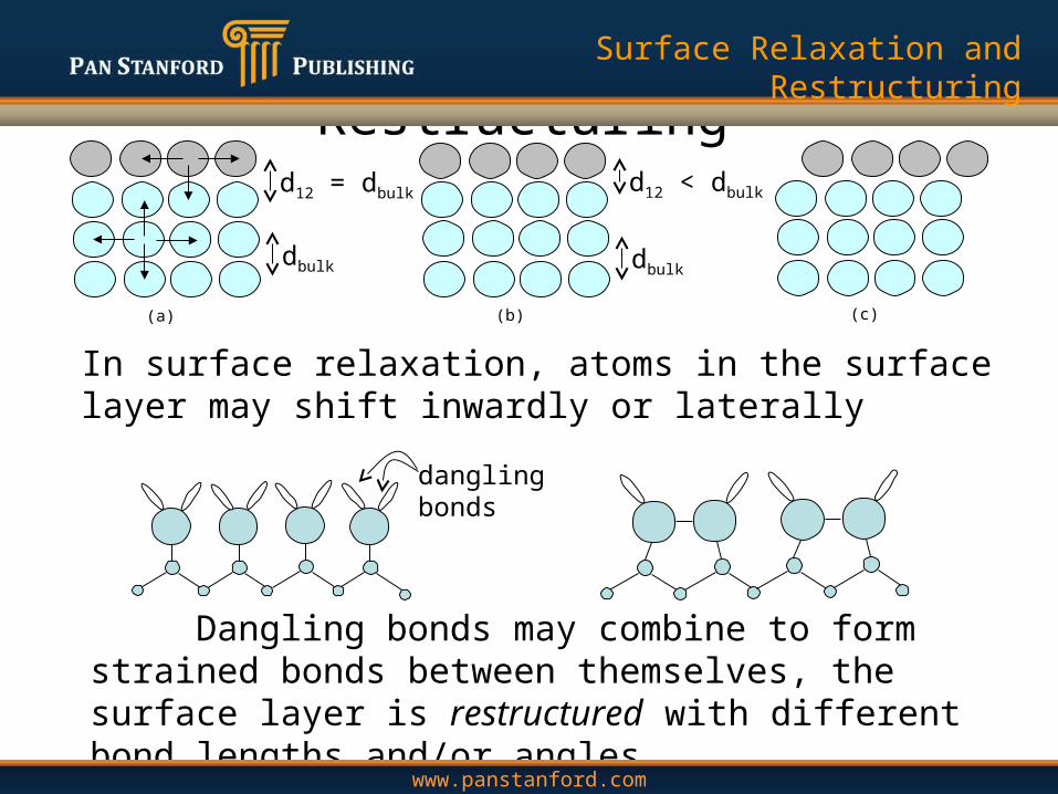
Surface Relaxation and Restructuring
In surface relaxation, atoms in the surface layer may shift inwardly or laterally
(c)(a)
d12 = dbulk
dbulk
(b)
d12 < dbulk
dbulk
dangling bonds
Dangling bonds may combine to form strained bonds between themselves, the surface layer is restructured with different bond lengths and/or angles.
www.panstanford.com
Surface Relaxation and Restructuring
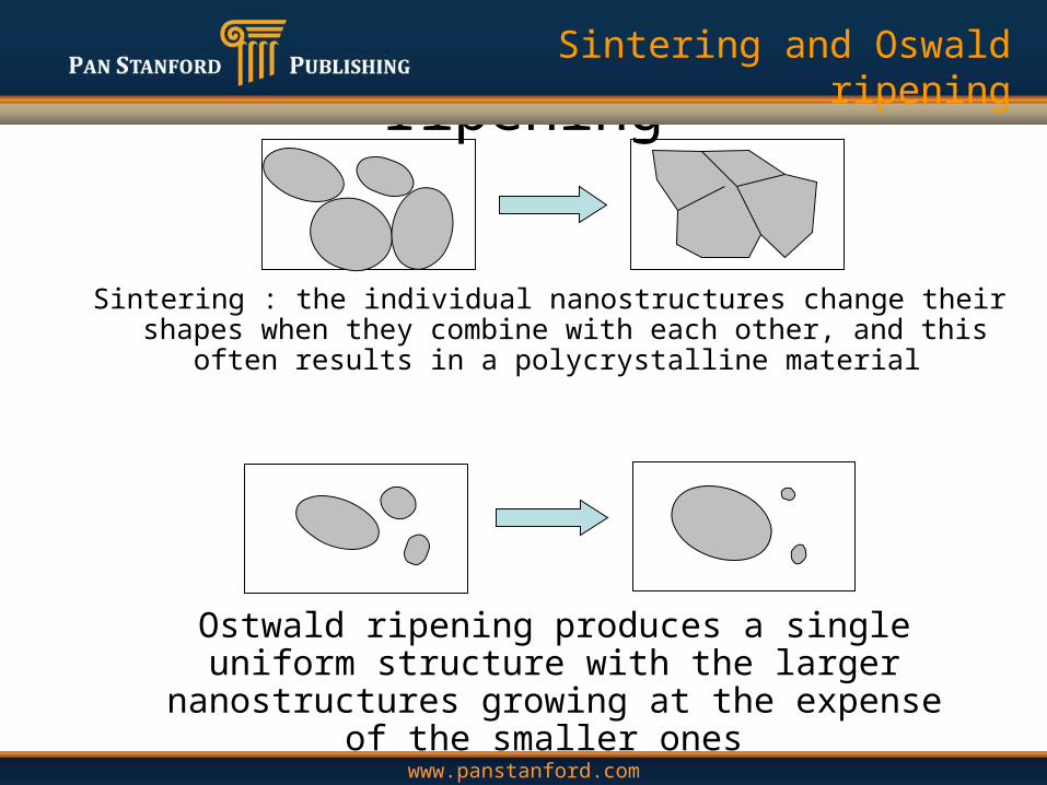
Sintering and Ostwald ripening
Sintering : the individual nanostructures change their shapes when they combine with each other, and this often results in a
polycrystalline material
Ostwald ripening produces a single uniform structure with the larger nanostructures growing at the expense of
the smaller ones
www.panstanford.com
Sintering and Oswald ripening

Catalysis at the Nanoscale
With kind permission from Springer Science Business Media: J.Phys. D, Atomic Resolution electron microscopy of small metal clustes, 19, 293 (1991), J.-O. Boyin and J.-O. Malm. Copyright © 1991, Springer Berlin/Heldelberg.
www.panstanford.com
Catalysis at the Nanoscale

The electrical double layer
Stern layer : the fairly immobile layer of ions that adhere strongly to
the particle surface
Guoy layer : a diffuse layer of oppositely charged mobile
ions that are attracted to the first layer
www.panstanford.com
The electrical double layer
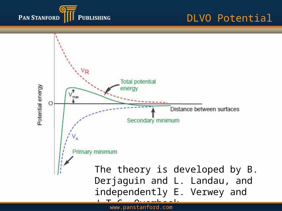
The theory is developed by B. Derjaguin and L. Landau, and independently E. Verwey and J.T.G. Overbeek.
DLVO potential
www.panstanford.com
DLVO Potential
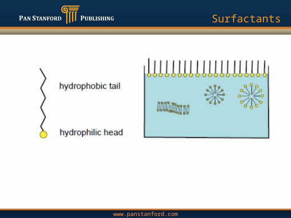
Surfactants
www.panstanford.com
Surfactants

AOT-water-isooctane system
www.panstanford.com
AOT-water-isooctane system

www.panstanford.com
Chapter 6

www.panstanford.com
Schematic of the energy bands
www.panstanford.com
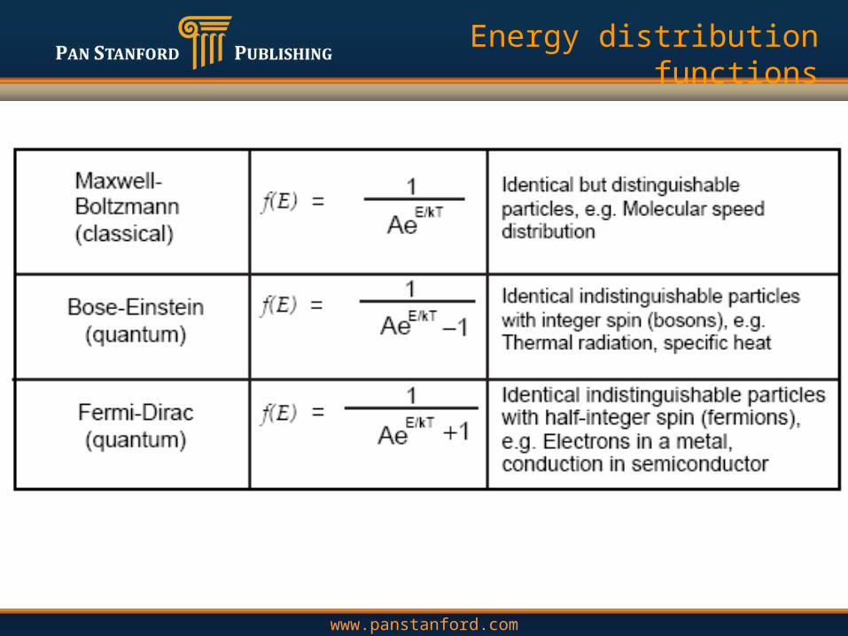
Energy distribution functions

Band structure of a semiconductor at different temperatures
www.panstanford.com
Band structure of a semiconductor at different temperatures
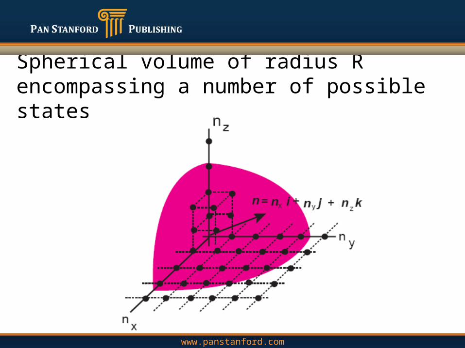
Spherical volume of radius R encompassing a number of possible states
www.panstanford.com

The functions f(E) and gc(E)
www.panstanford.com
The functions of f(E) and gc(E)

Density of states for 3D, 2D, 1D, and 0D structures
www.panstanford.com
Density of States
www.panstanford.com
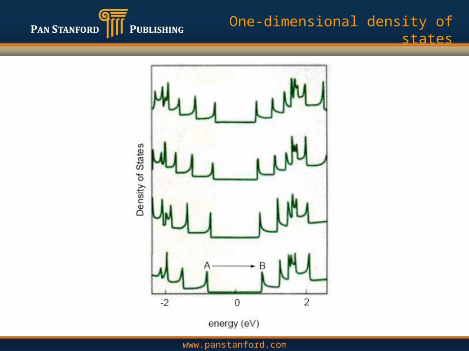
One-dimensional density of states

www.panstanford.com
GaAs/AlGaAs/GaAs heterostructure
Band diagram, i.e. the energy of the conduction band. The
dashed line is the Fermi energy
Cross-section through the heterostructure grown by MBE with nearly atomically sharp interfaces
www.panstanford.com
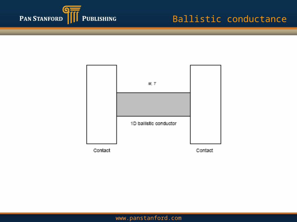
Ballistic conductance
www.panstanford.com
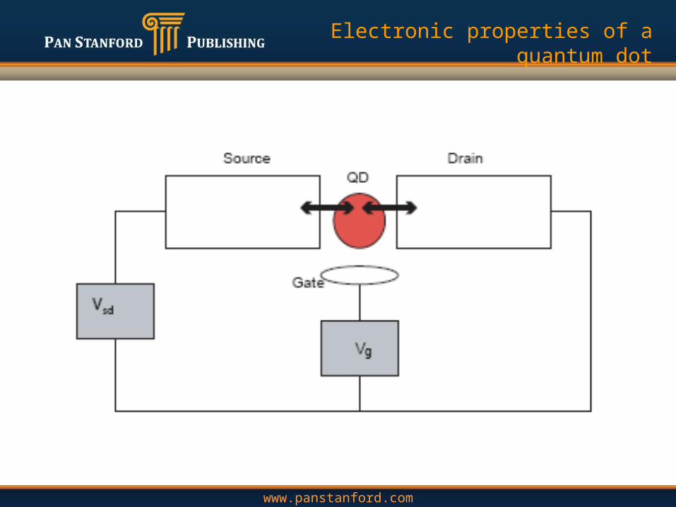
Electronic properties of a quantum dot
www.panstanford.com
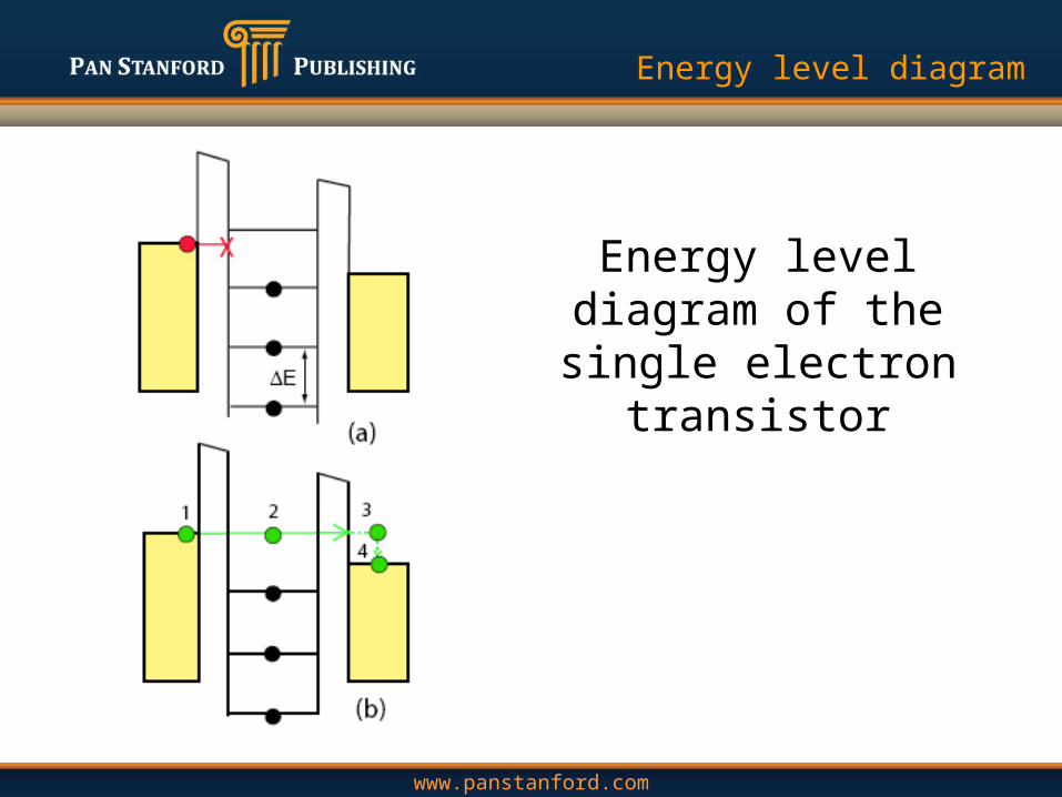
Energy level diagram
Energy level diagram of the single electron
transistor

www.panstanford.com
Chapter 7

www.panstanford.com
Variation of Gibbs energy during the nucleation process

www.panstanford.com
The nucleation and growth processes

www.panstanford.com
Effect of capping molecule
CdS nanocrystals produced with (a) higher and (b) lower amounts of the capping molecule
hexadecylamine
www.panstanford.com
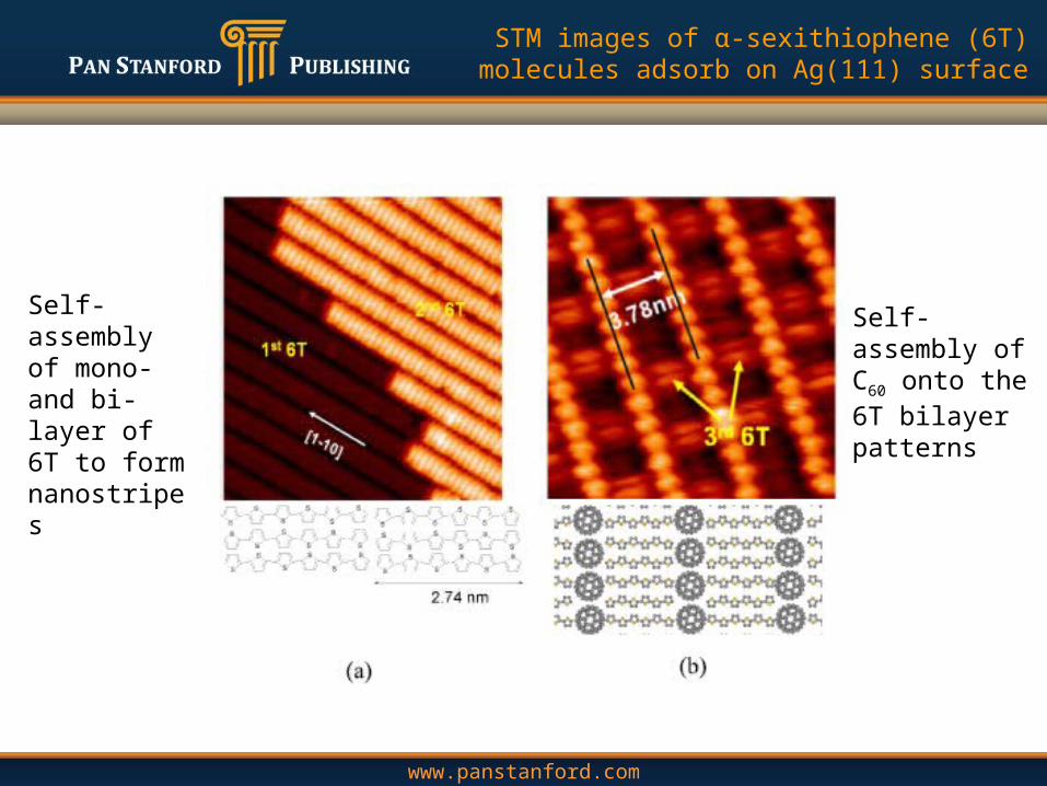
STM images of α-sexithiophene (6T) molecules adsorb on Ag(111) surface
Self-assembly of mono- and bi-layer of 6T to form nanostripes
Self-assembly of C60 onto the 6T bilayer patterns

www.panstanford.com
Self-assembled monolayers (SAMs)

www.panstanford.com
Close-packed Assembly
SEM images showingclose-packed assembly of micron-sized nanoparticles

www.panstanford.com
Capillary actions between particles
www.panstanford.com
Chapter 8
www.panstanford.com
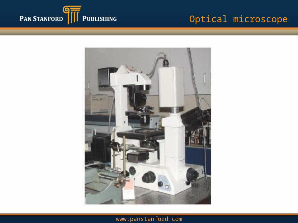
Optical microscope
www.panstanford.com
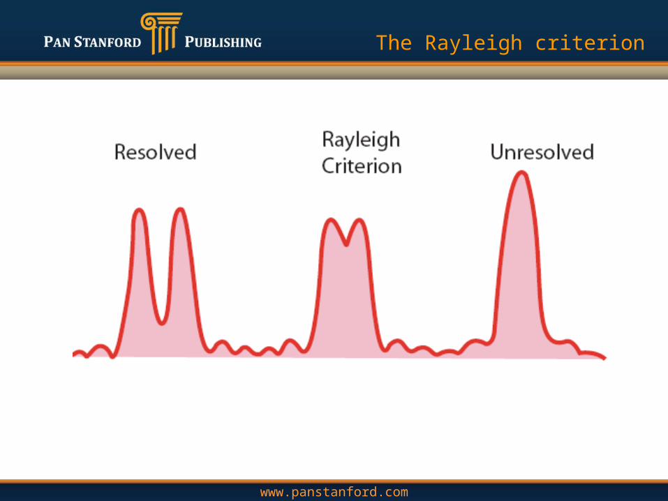
The Rayleigh criterion
www.panstanford.com
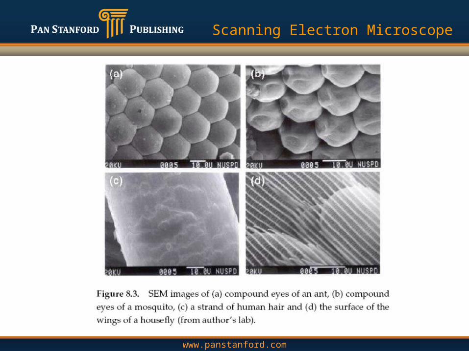
Scanning Electron Microscope
www.panstanford.com
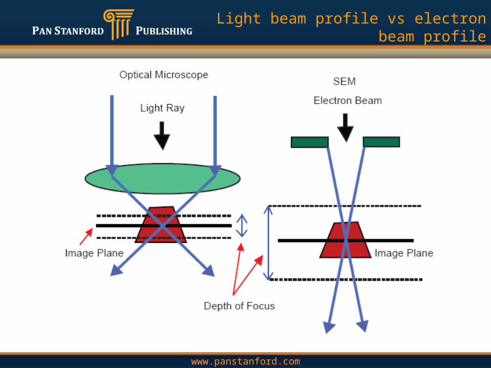
Light beam profile vs electron beam profile

www.panstanford.com
Main components of a SEM
www.panstanford.com
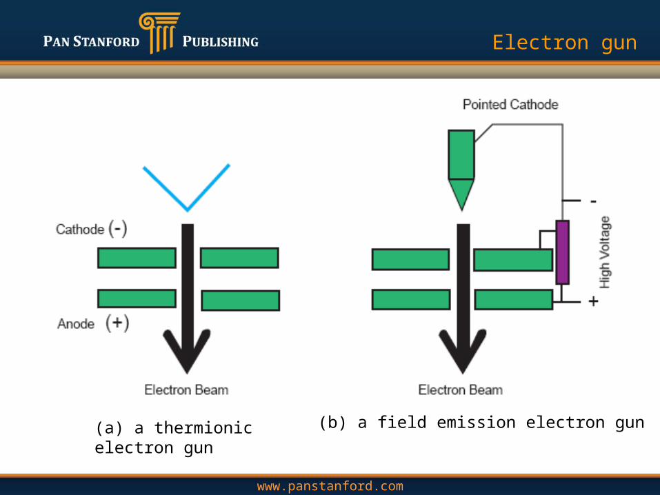
Electron gun
(a) a thermionic electron gun (b) a field emission electron gun
www.panstanford.com
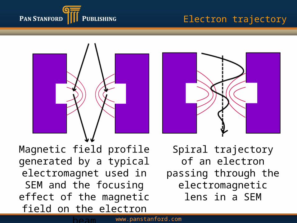
Electron trajectory
Spiral trajectory of an electron passing through
the electromagneticlens in a SEM
Magnetic field profile generated by a typical electromagnet used in SEM and the focusing effect
of the magnetic field on the electron beam

www.panstanford.com
Detectable signals generated when an energetic electronbeam is incident on a thick sample
www.panstanford.com
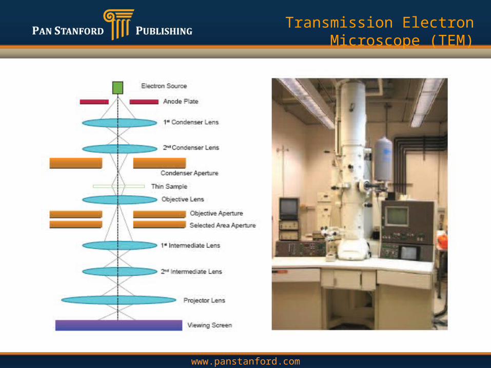
Transmission Electron Microscope (TEM)
www.panstanford.com
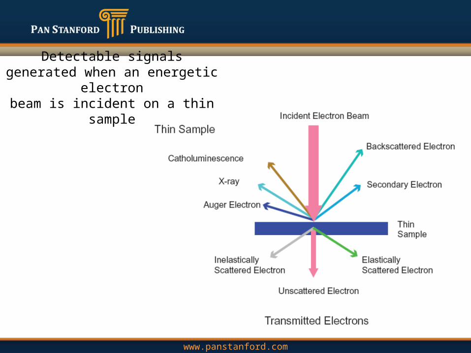
Detectable signals generated when an energetic electron
beam is incident on a thin sample
www.panstanford.com
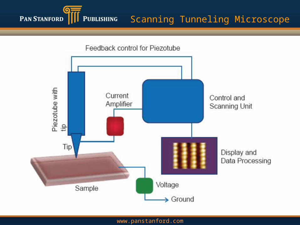
Scanning Tunneling Microscope
www.panstanford.com
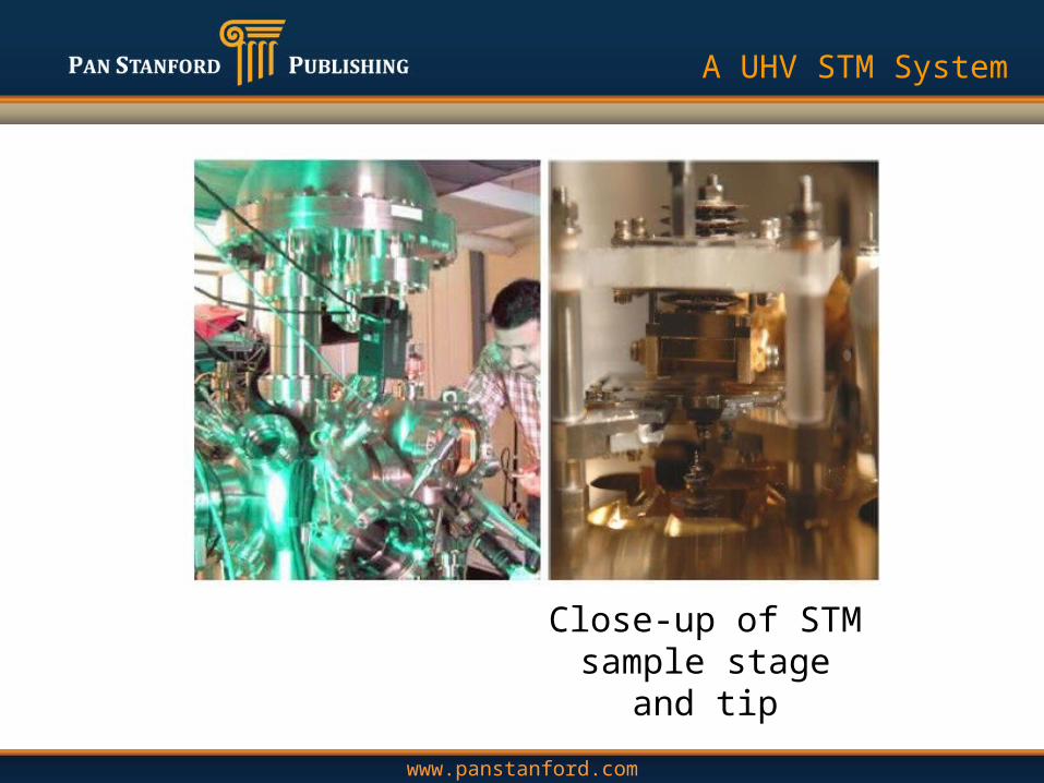
A UHV STM System
Close-up of STM sample stage and tip

www.panstanford.com
STM image of Si(111)-(7 × 7)

www.panstanford.com
www.panstanford.com
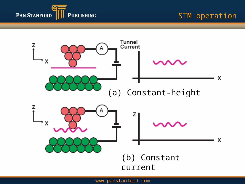
STM operation
(b) Constant current
(a) Constant-height
www.panstanford.com
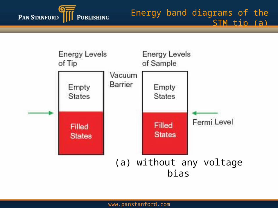
Energy band diagrams of the STM tip (a)
(a) without any voltage bias

www.panstanford.com
Energy band diagrams of the STM tip (b)
(b) when the tip is negatively biased with respect to the sample

www.panstanford.com
Energy band diagrams of the STM tip (c)
(c) when the tip is positively biased with respect to the sample

www.panstanford.com
Atomic Force Microscope
Image of the cantileverand probe tip
www.panstanford.com
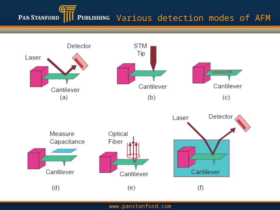
Various detection modes of AFM

www.panstanford.com
Optical Tweezer
www.panstanford.com
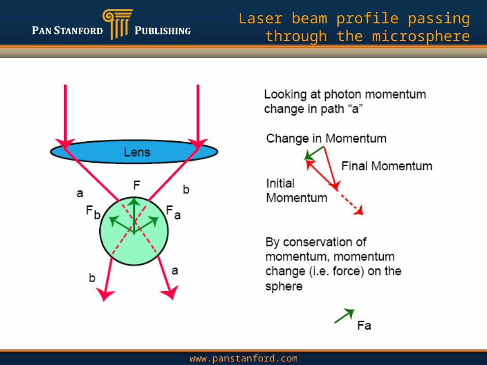
Laser beam profile passing through the microsphere
www.panstanford.com
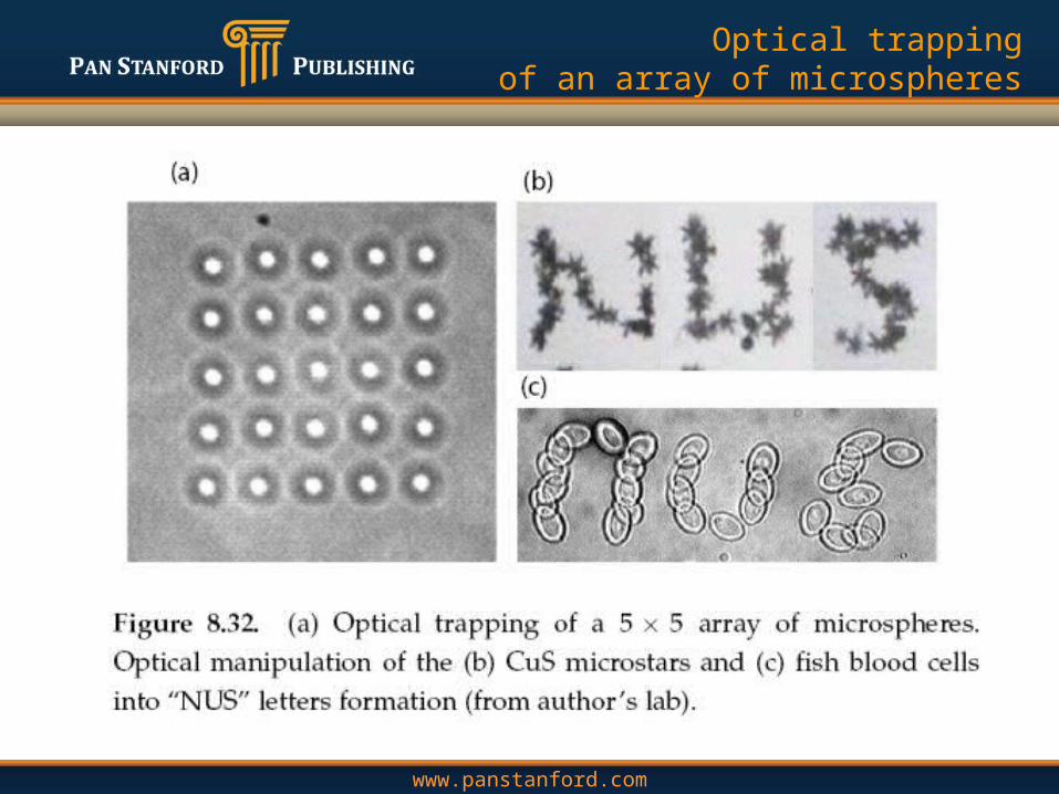
Optical trappingof an array of microspheres

www.panstanford.com