x-band 6-bit phase shifter with low rms phase …...512 jang-hoon han et al : x-band 6-bit phase...
TRANSCRIPT
JOURNAL OF SEMICONDUCTOR TECHNOLOGY AND SCIENCE, VOL.16, NO.4, AUGUST, 2016 ISSN(Print) 1598-1657 http://dx.doi.org/10.5573/JSTS.2016.16.4.511 ISSN(Online) 2233-4866
Manuscript received Dec. 22, 2015; accepted Apr. 10, 2016 1 Department of Electronic Engineering, Kwangwoon University, Gwangun-ro, Nowon-gu, Seoul, Korea 2 School of Electrical Engineering, Chung-Ang University, Heukseok-ro, Dongjak-gu, Seoul, Korea E-mail : [email protected]
X-Band 6-Bit Phase Shifter with Low RMS Phase and Amplitude Errors in 0.13-mm CMOS Technology
Jang-Hoon Han1, Jeong-Geun Kim1, and Donghyun Baek2
Abstract—This paper proposes a CMOS 6-bit phase shifter with low RMS phase and amplitude errors for an X-band phased array antenna. The phase shifter combines a switched-path topology for coarse phase states and a switch-filter topology for fine phase states. The coarse phase shifter is composed of phase shifting elements, single-pole double-throw (SPDT), and double-pole double-throw (DPDT) switches. The fine phase shifter uses a switched LC filter. The phase coverage is 354.35° with an LSB of 5.625°. The RMS phase error is < 6° and the RMS amplitude error is < 0.45 dB at 8–12 GHz. The measured insertion loss is < 15 dB, and the return losses for input and output are > 13 dB at 8–12 GHz. The input P1dB of the phase shifter achieves > 11 dBm at 8–12 GHz. The current consumption is zero with a 1.2-V supply voltage. The chip size is 1.46´0.83 mm2, including pads. Index Terms—X-band, phase shifter, phased array antenna, CMOS, SPDT, DPDT switch
I. INTRODUCTION
A phase shifter is a key component in the transmitter/receiver (T/R) module of a phased array antenna [1, 2]. Low insertion loss, low cost, and low power consumption are necessary properties for the phase shifter because a large number of phase shifters are
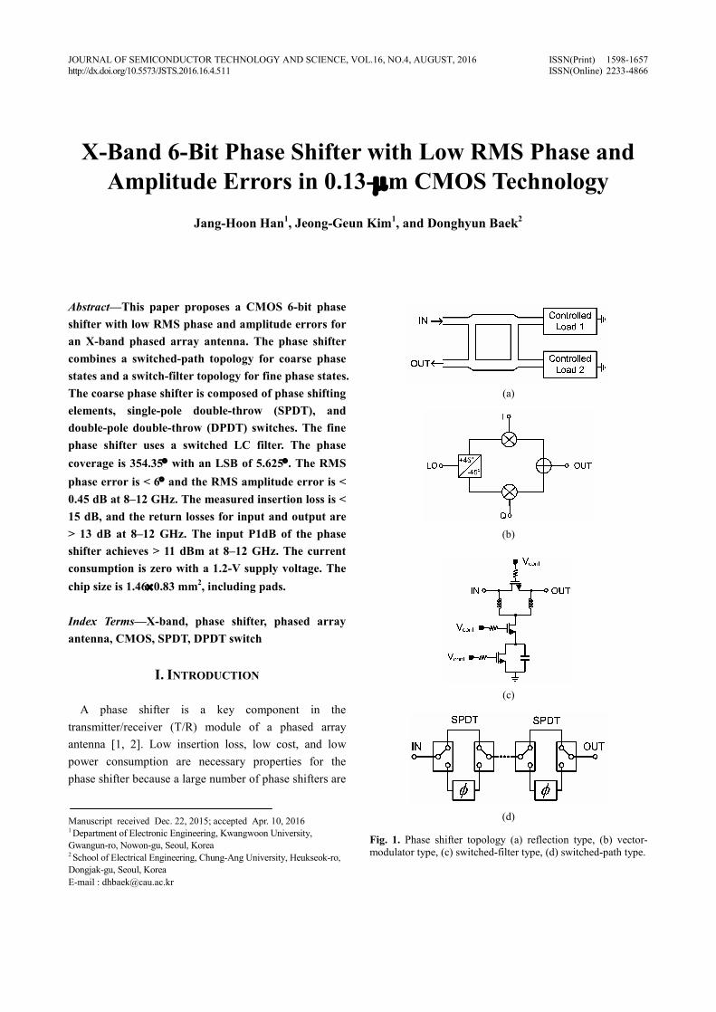
(a)
(b)
(c)
(d)
Fig. 1. Phase shifter topology (a) reflection type, (b) vector-modulator type, (c) switched-filter type, (d) switched-path type.
512 JANG-HOON HAN et al : X-BAND 6-BIT PHASE SHIFTER WITH LOW RMS PHASE AND AMPLITUDE ERRORS IN 0.13-mM …
employed in a phased array antenna. The reflection phase shifter shown in Fig. 1(a), which uses a 90° hybrid coupler and controlled capacitive loads, has been widely adopted in PCB-based designs [3, 4]. However, as the size of the phase shifter is determined by the size of the hybrid coupler, the reflection phase shifter is inappropriate for a compact phase array, and is difficult to integrate in a monolithic microwave integrated circuit (MMIC).
Recently, silicon-based phase shifters have been reported by many research groups. The vector-modulator and switched-filter topologies in Fig. 1(b) and (c) are widely used in silicon-based phase shifters [5-8]. The active vector-summing phase shifter has a compact size and high accuracy with digital calibration circuits. However, this type of phase shifter operates only in one direction. In addition, it has non-zero DC power consumption and lower linearity than the phase shifters using the switches due to the analog amplifiers [5].
The switched-path phase shifter uses the phase difference between two paths, as shown in Fig. 1(d) [9, 10]. The signal path is controlled by the switch circuit, and the phase difference is produced by a delay element in one path. This method has the widest potential bandwidth because the phase variation between the two paths within the frequency band of interest can be easily compensated. Moreover, this phase shifter operates bidirectionally [11-13]. Since the scanning accuracy of the beam former depends on the resolution of the phase shifter, the phase-shift quantization error reduces the signal-to-noise ratio (SNR) of the receiver at some
receiving angles. Therefore, it is important to reduce the phase error of the phase shifter to improve the SNR of the receiver.
In this study, an X-band 6-bit switched-path phase shifter with low RMS phase error and zero power consumption is presented in a standard 0.13-mm CMOS technology.
II. DESIGN OF X-BAND 6-BIT PHASE SHIFTER
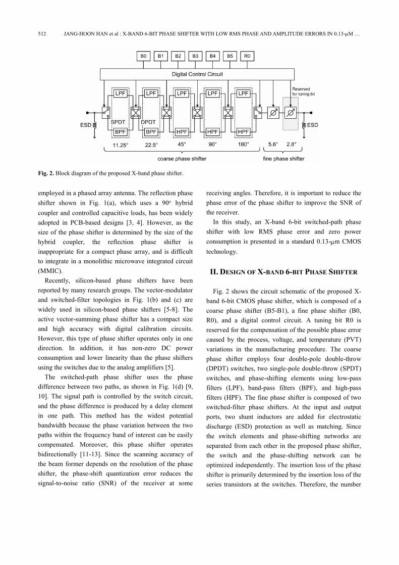
Fig. 2 shows the circuit schematic of the proposed X-band 6-bit CMOS phase shifter, which is composed of a coarse phase shifter (B5-B1), a fine phase shifter (B0, R0), and a digital control circuit. A tuning bit R0 is reserved for the compensation of the possible phase error caused by the process, voltage, and temperature (PVT) variations in the manufacturing procedure. The coarse phase shifter employs four double-pole double-throw (DPDT) switches, two single-pole double-throw (SPDT) switches, and phase-shifting elements using low-pass filters (LPF), band-pass filters (BPF), and high-pass filters (HPF). The fine phase shifter is composed of two switched-filter phase shifters. At the input and output ports, two shunt inductors are added for electrostatic discharge (ESD) protection as well as matching. Since the switch elements and phase-shifting networks are separated from each other in the proposed phase shifter, the switch and the phase-shifting network can be optimized independently. The insertion loss of the phase shifter is primarily determined by the insertion loss of the series transistors at the switches. Therefore, the number
Fig. 2. Block diagram of the proposed X-band phase shifter.
JOURNAL OF SEMICONDUCTOR TECHNOLOGY AND SCIENCE, VOL.16, NO.4, AUGUST, 2016 513
of cascaded series transistors in the RF signal path should be reduced to decrease the insertion loss.
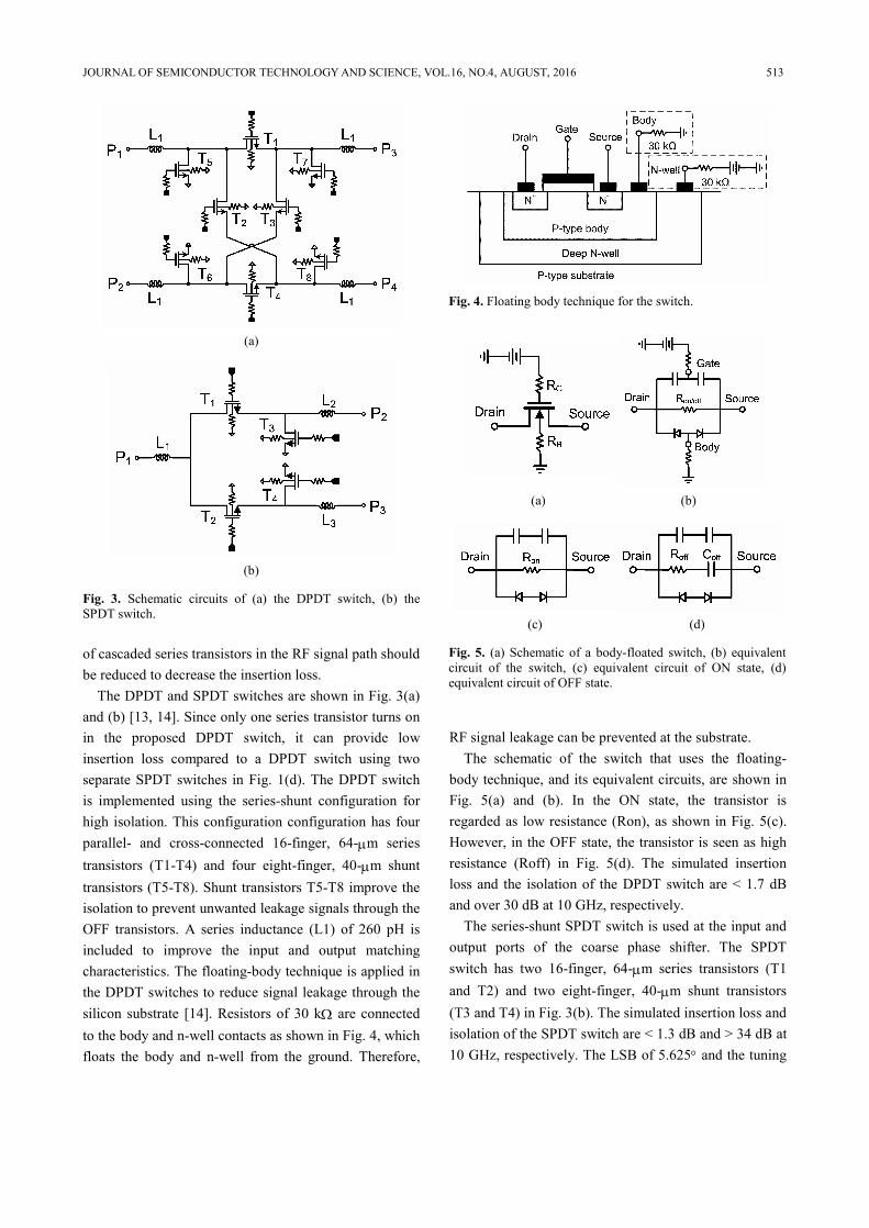
The DPDT and SPDT switches are shown in Fig. 3(a) and (b) [13, 14]. Since only one series transistor turns on in the proposed DPDT switch, it can provide low insertion loss compared to a DPDT switch using two separate SPDT switches in Fig. 1(d). The DPDT switch is implemented using the series-shunt configuration for high isolation. This configuration configuration has four parallel- and cross-connected 16-finger, 64-mm series transistors (T1-T4) and four eight-finger, 40-mm shunt transistors (T5-T8). Shunt transistors T5-T8 improve the isolation to prevent unwanted leakage signals through the OFF transistors. A series inductance (L1) of 260 pH is included to improve the input and output matching characteristics. The floating-body technique is applied in the DPDT switches to reduce signal leakage through the silicon substrate [14]. Resistors of 30 kW are connected to the body and n-well contacts as shown in Fig. 4, which floats the body and n-well from the ground. Therefore,
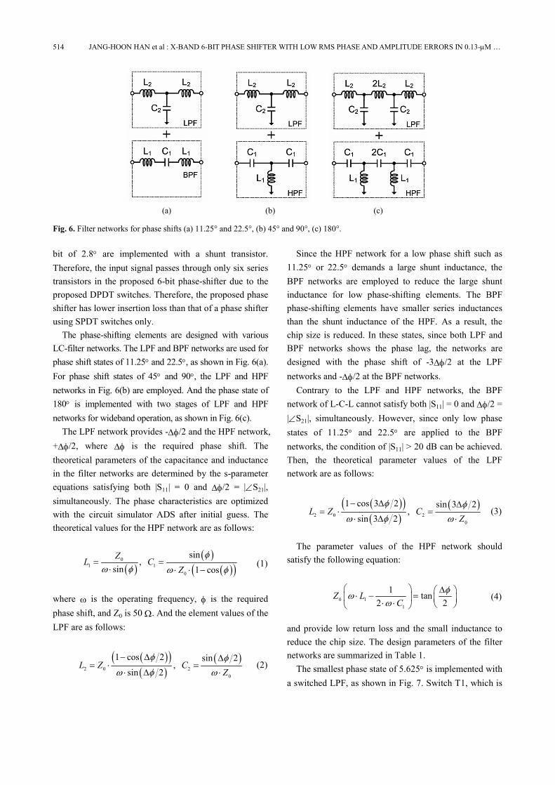
RF signal leakage can be prevented at the substrate. The schematic of the switch that uses the floating-
body technique, and its equivalent circuits, are shown in Fig. 5(a) and (b). In the ON state, the transistor is regarded as low resistance (Ron), as shown in Fig. 5(c). However, in the OFF state, the transistor is seen as high resistance (Roff) in Fig. 5(d). The simulated insertion loss and the isolation of the DPDT switch are < 1.7 dB and over 30 dB at 10 GHz, respectively.
The series-shunt SPDT switch is used at the input and output ports of the coarse phase shifter. The SPDT switch has two 16-finger, 64-mm series transistors (T1 and T2) and two eight-finger, 40-mm shunt transistors (T3 and T4) in Fig. 3(b). The simulated insertion loss and isolation of the SPDT switch are < 1.3 dB and > 34 dB at 10 GHz, respectively. The LSB of 5.625° and the tuning
(a)
(b)
Fig. 3. Schematic circuits of (a) the DPDT switch, (b) the SPDT switch.
Fig. 4. Floating body technique for the switch.
(a) (b)
(c) (d)
Fig. 5. (a) Schematic of a body-floated switch, (b) equivalent circuit of the switch, (c) equivalent circuit of ON state, (d) equivalent circuit of OFF state.
514 JANG-HOON HAN et al : X-BAND 6-BIT PHASE SHIFTER WITH LOW RMS PHASE AND AMPLITUDE ERRORS IN 0.13-mM …
bit of 2.8° are implemented with a shunt transistor. Therefore, the input signal passes through only six series transistors in the proposed 6-bit phase-shifter due to the proposed DPDT switches. Therefore, the proposed phase shifter has lower insertion loss than that of a phase shifter using SPDT switches only.
The phase-shifting elements are designed with various LC-filter networks. The LPF and BPF networks are used for phase shift states of 11.25° and 22.5°, as shown in Fig. 6(a). For phase shift states of 45° and 90°, the LPF and HPF networks in Fig. 6(b) are employed. And the phase state of 180° is implemented with two stages of LPF and HPF networks for wideband operation, as shown in Fig. 6(c).
The LPF network provides -Df/2 and the HPF network, +Df/2, where Df is the required phase shift. The theoretical parameters of the capacitance and inductance in the filter networks are determined by the s-parameter equations satisfying both |S11| = 0 and Df/2 = |ÐS21|, simultaneously. The phase characteristics are optimized with the circuit simulator ADS after initial guess. The theoretical values for the HPF network are as follows:
( )( )
( )( )0
1 10
sin,
sin 1 cosZ
L CZ
fw f w f
= =× × × -
(1)
where w is the operating frequency, f is the required phase shift, and Z0 is 50 W. And the element values of the LPF are as follows:
( )( )( )
( )2 0 2
0
1 cos 2 sin 2,
sin 2L Z C
Zf f
w f w
- D D= × =
× D × (2)
Since the HPF network for a low phase shift such as 11.25° or 22.5° demands a large shunt inductance, the BPF networks are employed to reduce the large shunt inductance for low phase-shifting elements. The BPF phase-shifting elements have smaller series inductances than the shunt inductance of the HPF. As a result, the chip size is reduced. In these states, since both LPF and BPF networks shows the phase lag, the networks are designed with the phase shift of -3Df/2 at the LPF networks and -Df/2 at the BPF networks.
Contrary to the LPF and HPF networks, the BPF network of L-C-L cannot satisfy both |S11| = 0 and Df/2 = |ÐS21|, simultaneously. However, since only low phase states of 11.25° and 22.5° are applied to the BPF networks, the condition of |S11| > 20 dB can be achieved. Then, the theoretical parameter values of the LPF network are as follows:
( )( )( )
( )2 0 2
0
1 cos 3 2 sin 3 2,
sin 3 2L Z C
Zf f
w f w
- D D= × =
× D × (3)
The parameter values of the HPF network should
satisfy the following equation:
0 11
1 tan2 2
Z LC
fww
æ ö Dæ ö× - =ç ÷ ç ÷× × è øè ø (4)
and provide low return loss and the small inductance to reduce the chip size. The design parameters of the filter networks are summarized in Table 1.
The smallest phase state of 5.625° is implemented with a switched LPF, as shown in Fig. 7. Switch T1, which is
(a) (b) (c)
Fig. 6. Filter networks for phase shifts (a) 11.25° and 22.5°, (b) 45° and 90°, (c) 180°.
JOURNAL OF SEMICONDUCTOR TECHNOLOGY AND SCIENCE, VOL.16, NO.4, AUGUST, 2016 515
serially connected with C1, controls the shunt capacitance. The phase shifter may exhibit some phase errors due to the inaccuracy of the device model or because of PVT variations. Therefore, a phase-tuning bit of 2.8° is included to compensate for this unwanted phase error. The tuning bit is implemented with the switched-LPF phase-shifting element also. Since the phase states of 5.625° and 2.8° are controlled only by the shunt transistors, there are no series transistors in the RF signal path. Therefore, low insertion loss can be achieved.
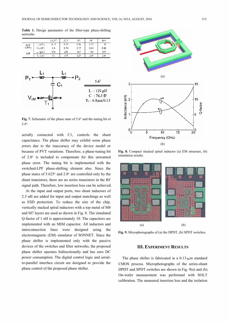
At the input and output ports, two shunt inductors of 2.5 nH are added for input and output matchings as well as ESD protection. To reduce the size of the chip, vertically stacked spiral inductors with a top metal of M8 and M7 layers are used as shown in Fig. 8. The simulated Q-factor of 1 nH is approximately 10. The capacitors are implemented with an MIM capacitor. All inductors and interconnection lines were designed using the electromagnetic (EM) simulator of SONNET. Since the phase shifter is implemented only with the passive devices of the switches and filter networks, the proposed phase shifter operates bidirectionally and has zero DC power consumption. The digital control logic and serial-to-parallel interface circuit are designed to provide the phase control of the proposed phase shifter.
III. EXPERIMENT RESULTS
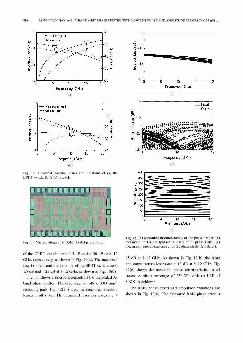
The phase shifter is fabricated in a 0.13-mm standard CMOS process. Microphotographs of the series-shunt DPDT and SPDT switches are shown in Fig. 9(a) and (b). On-wafer measurement was performed with SOLT calibration. The measured insertion loss and the isolation
Table 1. Design parameters of the filter-type phase-shifting networks
Fig. 7. Schematic of the phase state of 5.6° and the tuning bit of 2.8°.
(a)
(b)
Fig. 8. Compact stacked spiral inductor (a) EM structure, (b) simulation results.
(a) (b)
Fig. 9. Microphotographs of (a) the DPDT, (b) SPDT switches.
516 JANG-HOON HAN et al : X-BAND 6-BIT PHASE SHIFTER WITH LOW RMS PHASE AND AMPLITUDE ERRORS IN 0.13-mM …
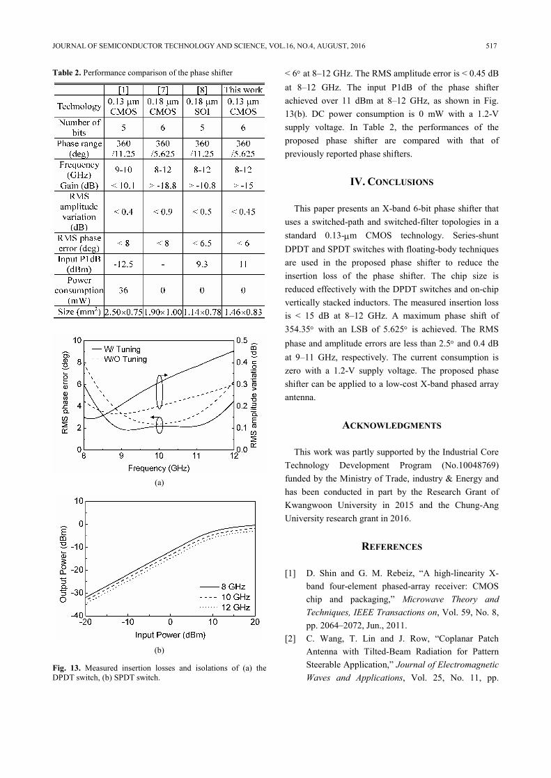
of the DPDT switch are < 1.5 dB and > 30 dB at 8–12 GHz, respectively, as shown in Fig. 10(a). The measured insertion loss and the isolation of the SPDT switch are < 1.8 dB and > 25 dB at 8–12 GHz, as shown in Fig. 10(b).
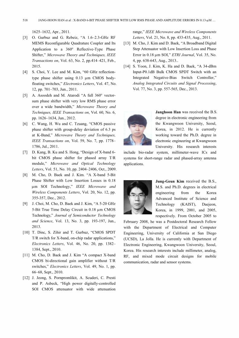
Fig. 11 shows a microphotograph of the fabricated X-band phase shifter. The chip size is 1.46 ´ 0.83 mm2, including pads. Fig. 12(a) shows the measured insertion losses in all states. The measured insertion losses are <
15 dB at 8–12 GHz. As shown in Fig. 12(b), the input and output return losses are > 13 dB at 8–12 GHz. Fig. 12(c) shows the measured phase characteristics in all states. A phase coverage of 354.35° with an LSB of 5.625° is achieved.
The RMS phase errors and amplitude variations are shown in Fig. 13(a). The measured RMS phase error is
(a)
(b)
Fig. 10. Measured insertion losses and isolations of (a) the DPDT switch, (b) SPDT switch.
Fig. 11. Microphotograph of X-band 6-bit phase shifter.
(a)
(b)
(c)
Fig. 12. (a) Measured insertion losses of the phase shifter, (b) measured input and output return losses of the phase shifter, (c) measured phase characteristics of the phase shifter (all states).
JOURNAL OF SEMICONDUCTOR TECHNOLOGY AND SCIENCE, VOL.16, NO.4, AUGUST, 2016 517
< 6° at 8–12 GHz. The RMS amplitude error is < 0.45 dB at 8–12 GHz. The input P1dB of the phase shifter achieved over 11 dBm at 8–12 GHz, as shown in Fig. 13(b). DC power consumption is 0 mW with a 1.2-V supply voltage. In Table 2, the performances of the proposed phase shifter are compared with that of previously reported phase shifters.
IV. CONCLUSIONS
This paper presents an X-band 6-bit phase shifter that uses a switched-path and switched-filter topologies in a standard 0.13-mm CMOS technology. Series-shunt DPDT and SPDT switches with floating-body techniques are used in the proposed phase shifter to reduce the insertion loss of the phase shifter. The chip size is reduced effectively with the DPDT switches and on-chip vertically stacked inductors. The measured insertion loss is < 15 dB at 8–12 GHz. A maximum phase shift of 354.35° with an LSB of 5.625° is achieved. The RMS phase and amplitude errors are less than 2.5° and 0.4 dB at 9–11 GHz, respectively. The current consumption is zero with a 1.2-V supply voltage. The proposed phase shifter can be applied to a low-cost X-band phased array antenna.
ACKNOWLEDGMENTS
This work was partly supported by the Industrial Core Technology Development Program (No.10048769) funded by the Ministry of Trade, industry & Energy and has been conducted in part by the Research Grant of Kwangwoon University in 2015 and the Chung-Ang University research grant in 2016.
REFERENCES
[1] D. Shin and G. M. Rebeiz, “A high-linearity X-band four-element phased-array receiver: CMOS chip and packaging,” Microwave Theory and Techniques, IEEE Transactions on, Vol. 59, No. 8, pp. 2064–2072, Jun., 2011.
[2] C. Wang, T. Lin and J. Row, “Coplanar Patch Antenna with Tilted-Beam Radiation for Pattern Steerable Application,” Journal of Electromagnetic Waves and Applications, Vol. 25, No. 11, pp.
Table 2. Performance comparison of the phase shifter
(a)
(b)
Fig. 13. Measured insertion losses and isolations of (a) the DPDT switch, (b) SPDT switch.
518 JANG-HOON HAN et al : X-BAND 6-BIT PHASE SHIFTER WITH LOW RMS PHASE AND AMPLITUDE ERRORS IN 0.13-mM …
1625–1632, Apr., 2011. [3] O. Gurbuz and G. Rebeiz, “A 1.6–2.3-GHz RF
MEMS Reconfigurable Quadrature Coupler and Its Application to a 360° Reflective-Type Phase Shifter,” Microwave Theory and Techniques, IEEE Transactions on, Vol. 63, No. 2, pp.414–421, Feb., 2015.
[4] S. Choi, Y. Lee and M. Kim, “60 GHz reflection-type phase shifter using 0.13 mm CMOS body-floating switches,” Electronics Letters, Vol. 47, No. 12, pp. 701–703, Jun., 2011.
[5] A. Asoodeh and M. Atarodi “A full 360° vector-sum phase shifter with very low RMS phase error over a wide bandwidth,” Microwave Theory and Techniques, IEEE Transactions on, Vol. 60, No. 6, pp. 1626–1634, Jun., 2012.
[6] C. Wang, H. Wu and C. Tzuang, “CMOS passive phase shifter with group-delay deviation of 6.3 ps at K-Band,” Microwave Theory and Techniques, IEEE Transactions on, Vol. 59, No. 7, pp. 1778–1786, Jul., 2011.
[7] D. Kang, B. Ku and S. Hong, “Design of X-band 6-bit CMOS phase shifter for phased array T/R module,” Microwave and Optical Technology Letters, Vol. 51, No. 10, pp. 2404–2406, Oct., 2009.
[8] M. Cho, D. Baek and J. Kim. “A X-band 5-Bit Phase Shifter with Low Insertion Losses in 0.18 mm SOI Technology,” IEEE Microwave and Wireless Components Letters, Vol. 20, No. 12, pp. 355-357, Dec., 2012.
[9] J. Choi, M. Cho, D. Baek and J. Kim, “A 5-20 GHz 5-Bit True Time Delay Circuit in 0.18 mm CMOS Technology,” Journal of Semiconductor Technology and Science, Vol. 13, No. 3, pp. 193-197, Jun., 2013.
[10] T. Dinc, S. Zihir and T. Gurbuz, “CMOS SPDT T/R switch for X-band, on-chip radar applications,” Electronics Letters, Vol. 46, No. 20, pp. 1382–1384, Sept., 2010.
[11] M. Cho, D. Baek and J. Kim “A compact X-band CMOS bi-directional gain amplifier without T/R switches,” Electronics Letters, Vol. 49, No. 1, pp. 66–68, Sept., 2010.
[12] J. Jeong, S. Pornpromlikit, A. Scuderi, C. Presti and P. Asbeck, “High power digitally-controlled SOI CMOS attenuator with wide attenuation
range,” IEEE Microwave and Wireless Components Letters, Vol. 21, No. 8, pp. 433-435, Aug., 2011.
[13] M. Cho, J. Kim and D. Baek, “A Broadband Digital Step Attenuator with Low Insertion Loss and Phase Error in 0.18 mm SOI,” ETRI Journal, Vol. 35, No. 4, pp. 638-643, Aug., 2013..
[14] S. Yoon, J. Kim, K. Ha and D. Baek, “A 34-dBm Input-P0.1dB Bulk CMOS SPDT Switch with an Integrated Negative-Bias Switch Controller,” Analog Integrated Circuits and Signal Processing, Vol. 77, No. 3, pp. 557-565, Dec., 2013.
Janghoon Han was received the B.S. degree in electronic engineering from the Kwangwoon University, Seoul, Korea, in 2012. He is currently working toward the Ph.D. degree in electronic engineering at Kwangwoon University. His research interests
include bio-radar system, millimeter-wave ICs and systems for short-range radar and phased-array antenna applications.
Jung-Geun Kim received the B.S., M.S. and Ph.D. degrees in electrical engineering from the Korea Advanced Institute of Science and Technology (KAIST), Daejeon, Korea, in 1999, 2001, and 2005, respectively. From October 2005 to
February 2008, he was a Postdoctoral Research Fellow with the Department of Electrical and Computer Engineering, University of California at San Diego (UCSD), La Jolla. He is currently with Department of Electronic Engineering, Kwangwoon University, Seoul, Korea. His research interests include millimeter, analog, RF, and mixed mode circuit designs for mobile communication, radar and sensor systems.
JOURNAL OF SEMICONDUCTOR TECHNOLOGY AND SCIENCE, VOL.16, NO.4, AUGUST, 2016 519
Donghyun Baek received the B.S., M.S., and Ph.D. degrees in the department of electrical engineering, Korea Advanced Institute of Science and Technology (KAIST), Daejeon, Korea, in 1996, 1998, and 2003, respectively. From 2003 to 2007, he
was a senior engineer with the System LSI Division, Samsung Electronics, Ki-heung, Korea, where he was engaged in mobile broadcasting RF receiver design and led the CMOS power amplifier project for handsets. In 2007, He joined the school of Electrical Engineering, Chung-Ang University, Seoul, Korea, where he is currently an associate professor. His research interests include analog, RF, and mixed mode circuit designs for mobile communication, radar and sensor systems.