xfp laser control and digital diagnostic ic - maxim integrated · digital diagnostics in optical...
TRANSCRIPT
General DescriptionThe DS1862 is a closed-loop laser-driver control IC withbuilt-in digital diagnostics designed for XFP MSA. Thelaser control function incorporates automatic powercontrol (APC) and allows extinction ratio control thougha temperature-indexed lookup table (LUT). The DS1862monitors up to seven analog inputs, including tempera-ture and monitor diode (MD) current, which are used toregulate the laser bias current and extinction ratio.Warning and alarm thresholds can be programmed togenerate an interrupt if monitored signals exceed toler-ance. Calibration is also provided internally using inde-pendent gain and offset scaling registers for each ofthe monitored analog signals. Settings such as pro-grammed calibration data are stored in password-pro-tected EEPROM memory. Programming is accomplishedthrough an I2C-compatible interface, which can also beused to access diagnostic functionality.
ApplicationsLaser Control and Monitoring 10Gbps OpticalTransceiver Modules (XFP)
Laser Control and Monitoring
Digital Diagnostics in Optical Transmission
Features♦ Implements XFP MSA Requirements for Digital
Diagnostics, Serial ID, and User Memory
♦ I2C-Compatible Serial Interface
♦ Automatic Power Control (APC)
♦ Extinction Ratio Control with Lookup Table
♦ Seven Monitored Channels for Digital Diagnostics(Five Basic Plus Two Auxiliary)
♦ Internal Calibration of Monitored Channels (Temp, VCC2/3, Bias Current, Transmitted, andReceived Power)
♦ Programmable Quick-Trip Logic for Turning Off Laser for Eye Safety
♦ Access to Monitoring and ID Information
♦ Programmable Alarm and Warning Thresholds
♦ Operates from 3.3V or 5V Supply
♦ 25-Ball CSBGA, 5mm x 5mm Package
♦ Internal or External Temperature Sensor
♦ -40°C to +100°C Operating Temperature Range
♦ One 8-Bit Buffered DAC
DS
18
62
XFP Laser Control and Digital Diagnostic IC
______________________________________________ Maxim Integrated Products 1
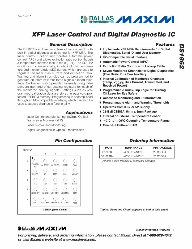
CSBGA (5mm x 5mm)
TOP VIEW
A
B
C
D
E
1 42 3 5
P-DOWN/RST
SC-RX-LOS SC-RX-LOL THRSET
RSSI MODSETSCLRX-LOS FETG
EN2 BIASSETSDATX-D EN1
AUX2MON BMDMOD-NRINTERRUPT AUX1MON
SC-TX-LOS VCC3MOD-DESELGND IBIASMON
VCC2
Pin Configuration
Rev 1; 12/07
For pricing, delivery, and ordering information, please contact Maxim Direct at 1-888-629-4642,or visit Maxim’s website at www.maxim-ic.com.
+Denotes a lead-free/RoHS-compliant package.
Ordering Information
Typical Operating Circuit appears at end of data sheet.
PART TEMP RANGE PIN-PACKAGE
DS1862B -40°C to +100°C 25 CSBGA
DS1862B+ -40°C to +100°C 25 CSBGA

DS
18
62
XFP Laser Control and Digital Diagnostic IC
2 _____________________________________________________________________
ABSOLUTE MAXIMUM RATINGS
RECOMMENDED OPERATING CONDITIONS(VCC3 = +2.9V to +5.5V, TA = -40°C to +100°C, unless otherwise noted.)
Stresses beyond those listed under “Absolute Maximum Ratings” may cause permanent damage to the device. These are stress ratings only, and functionaloperation of the device at these or any other conditions beyond those indicated in the operational sections of the specifications is not implied. Exposure toabsolute maximum rating conditions for extended periods may affect device reliability.
Voltage Range on Any Open-Drain Pin Relative to Ground.............................................-0.5V to +6.0V
Voltage Range on MOD-DESEL, SDA, SCL,FETG, THRSET, TX-D, AUX1MON, AUX2MON,IBIASMON, RSSI, BIASSET, MODSET,EN1, EN2............................................-0.5V to (VCC3 + 0.5V)*
Voltage Range on SC-RX-LOS, SC-RX-LOL, RX-LOS, SC-TX-LOS,MOD-NR, EN1, EN2 ...........................-0.5V to (VCC2 + 0.5V)*
Operating Temperature Range .........................-40°C to +100°CEEPROM Programming Temperature Range .........0°C to +70°CStorage Temperature Range .............................-55°C to +125°CSoldering Temperature...........................Refer to the IPC JEDEC
J-STD-020 Specification.
PARAMETER SYMBOL CONDITIONS MIN TYP MAX UNITS
Main Supply Voltage VCC3 (Note 1) +2.9 +5.5 V
Secondary Supply Voltage VCC2 VCC2 not to exceed VCC3 (Note 2) +1.6 +3.6 V
High-Level Input Voltage (SDA, SCL)
VIH IIH (max) = 10μA 0.7 x VCC3
VCC3 + 0.5
V
Low-Level Input Voltage (SDA, SCL)
VIL IIL (max) = -10μA GND -
0.3 0.3 x VCC3
V
High-Level Input Voltage (TX-D, MOD-DESEL, P-DOWN/RST) (Note 3)
VIH IIH (max) = 10μA 2 VCC3 +
0.3 V
Low-Level Input Voltage (TX-D, MOD-DESEL, P-DOWN/RST) (Note 3)
VIL IIL (max) = -10μA -0.3 +0.8 V
*Not to exceed +6.0V.
DS
18
62
XFP Laser Control and Digital Diagnostic IC
_____________________________________________________________________ 3
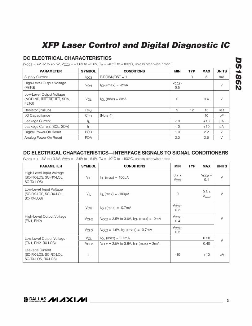
DC ELECTRICAL CHARACTERISTICS(VCC3 = +2.9V to +5.5V, VCC2 = +1.6V to +3.6V, TA = -40°C to +100°C, unless otherwise noted.)
PARAMETER SYMBOL CONDITIONS MIN TYP MAX UNITS
Supply Current ICC3 P-DOWN/RST = 1 3 5 mA
High-Level Output Voltage (FETG)
VOH IOH (max) = -2mA VCC3 -
0.5 V
Low-Level Output Voltage (MOD-NR, INTERRUPT, SDA, FETG)
VOL IOL (max) = 3mA 0 0.4 V
Resistor (Pullup) RPU 9 12 15 k
I/O Capacitance CI/O (Note 4) 10 pF
Leakage Current IL -10 +10 μA
Leakage Current (SCL, SDA) IL -10 +10 μA
Digital Power-On Reset POD 1.0 2.2 V
Analog Power-On Reset POA 2.0 2.6 V
DC ELECTRICAL CHARACTERISTICS—INTERFACE SIGNALS TO SIGNAL CONDITIONERS(VCC2 = +1.6V to +3.6V, VCC3 = +2.9V to +5.5V, TA = -40°C to +100°C, unless otherwise noted.)
PARAMETER SYMBOL CONDITIONS MIN TYP MAX UNITS
High-Level Input Voltage (SC-RX-LOS, SC-RX-LOL, SC-TX-LOS)
VIH IIH (max) = 100μA 0.7 x VCC2
VCC2 + 0.1
V
Low-Level Input Voltage (SC-RX-LOS, SC-RX-LOL, SC-TX-LOS)
VIL IIL (max) = -100μA 0 0.3 x VCC2
V
VOH IOH (max) = -0.7mA VCC2 -
0.2
VOH2 VCC2 = 2.5V to 3.6V, IOH (max) = -2mA VCC2 -
0.4 High-Level Output Voltage (EN1, EN2)
VOH3 VCC2 = 1.6V, IOH (max) = -0.7mA VCC2 -
0.2
V
VOL IOL (max) = 0.7mA 0.20 Low-Level Output Voltage (EN1, EN2, RX-LOS) VOL2 VCC2 = 2.5V to 3.6V, IOL (max) = 2mA 0.40
V
Leakage Current (SC-RX-LOS, SC-RX-LOL, SC-TX-LOS, RX-LOS)
IL -10 +10 μA
DS
18
62
XFP Laser Control and Digital Diagnostic IC
4 _____________________________________________________________________
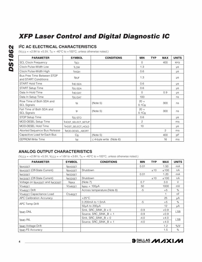
I2C AC ELECTRICAL CHARACTERISTICS(VCC3 = +2.9V to +5.5V, TA = -40°C to +100°C, unless otherwise noted.)
PARAMETER SYMBOL CONDITIONS MIN TYP MAX UNITS
SCL Clock Frequency fSCI 0 400 kHz
Clock Pulse-Width Low tLOW 1.3 μs
Clock Pulse-Width High tHIGH 0.6 μs
Bus Free Time Between STOP and START Conditions
tBUF 1.3 μs
START Hold Time tHD:SDA 0.6 μs
START Setup Time tSU:SDA 0.6 μs
Data In Hold Time tHD:DAT 0 0.9 μs
Data In Setup Time tSU:DAT 100 ns
Rise Time of Both SDA and SCL Signals
tR (Note 5) 20 + 0.1CB
300 ns
Fall Time of Both SDA and SCL Signals
tF (Note 5) 20 + 0.1CB
300 ns
STOP Setup Time tSU:STO 0.6 μs
MOD-DESEL Setup Time tHOST_SELECT_SETUP 2 ms
MOD-DESEL Hold Time tHOST_SELECT_HOLD 10 μs
Aborted Sequence Bus Release tMOD-DESEL_ABORT 2 ms
Capacitive Load for Each Bus CB (Note 5) 400 pF
EEPROM Write Time tW 4-byte write (Note 6) 16 ms
ANALOG OUTPUT CHARACTERISTICS(VCC3 = +2.9V to +5.5V, VCC2 = +1.6V to +3.6V, TA = -40°C to +100°C, unless otherwise noted.)
PARAMETER SYMBOL CONDITIONS MIN TYP MAX UNITS
IBIASSET IBIASSET 0.01 1.50 mA IBIASSET (Off-State Current) IBIASSET Shutdown ±10 ±100 nA IMODSET IMODSET 0.01 1.20 mA IMODSET (Off-State Current) IMODSET Shutdown ±10 ±100 nA Voltage on IBIASSET and IMODSET VMAX (Note 7) 0.7 3.0 V VTHRSET VTHRSET IMAX = 100μA 50 1000 mV VTHRSET Drift Across temperature (Note 8) -5 +5 % VTHRSET Capacitance Load CTHRSET 1 nF APC Calibration Accuracy +25°C 25 μA
0.200mA to 1.5mA -5 +5 % APC Temp Drift
50μA to 200μA 12 μA Sink, SRC_SINK_B = 0 -0.9 +0.9
IBMD DNL Source, SRC_SINK_B = 1 -0.9 +0.9
LSB
Sink, SRC_SINK_B = 0 -4.0 +4.0 IBMD INL
Source, SRC_SINK_B = 1 -4.0 +4.0 LSB
IBMD Voltage Drift 1.2 %/V IBMD FS Accuracy 1.5 %

DS
18
62
XFP Laser Control and Digital Diagnostic IC
_____________________________________________________________________ 5
PARAMETER SYMBOL CONDITIONS MIN TYP MAX UNITS
Time to Initialize tINIT VCC3 within ±5% of nominal 30 200 ms
TX-D Assert Time tOFF IBIAS and IMOD below 10% of nominal 5 μs
TX-D Deassert Time tON IBIAS and IMOD above 90% of nominal 1 ms
P-DOWN/RST Assert Time tPDR-ON IBIAS and IMOD below 10% of nominal 100 μs
P-DOWN/RST Deassert Time tPDR-OFF IBIAS and IMOD above 90% of nominal 200 ms
MOD-DESEL Deassert Time tMOD-DESELTime until proper response to I2Ccommunication
2 ms
INTERRUPT Assert Delay tINIT_ON Time from fault to interrupt assertion 100 ms
INTERRUPT Deassert Delay tINIT_OFFTime from read (clear flags) to interrupt deassertion
500 μs
MOD-NR Assert Delay tMOD-NR-ON Time from fault to MOD-NR assertion 0.5 ms
MOD-NR Deassert Delay tMOD-NR-OFFTime from read (clear flags) to MOD-NR deassertion
0.5 ms
RX-LOS Assert Time tLOS-ONTime from SC-RX-LOS assertion to RX-LOS assertion
100 ns
RX-LOS Deassert Time tLOS-OFFTime from SC-RX-LOS deassertion to RX-LOS deassertion
100 ns
P-DOWN/RST Reset Time tRESETTime from P-DOWN/RST assertion to initial reset
10 μs
Shutdown Time tFAULTTime from fault to IBIASSET, IMODSET,and IBMD below 10%
30 μs
ANALOG OUTPUT CHARACTERISTICS (continued)(VCC3 = +2.9V to +5.5V, VCC2 = +1.6V to +3.6V, TA = -40°C to +100°C, unless otherwise noted.)
PARAMETER SYMBOL CONDITIONS MIN TYP MAX UNITS
IMODSET Accuracy +25°C, IMODSET = 0.04mA to 1.2mA -1.5 +1.5 %
75μA range -0.9 +0.9 150μA range -0.9 +0.9 300μA range -0.9 +0.9 600μA range -0.9 +0.9
IMODSET DNL
1200μA range -0.9 +0.9
LSB
75μA range -1.5 +1.5 150μA range -1.5 +1.5 300μA range -1.0 +1.0 600μA range -1.0 +1.0
IMODSET INL
1200μA range -1.0 +1.0
LSB
IMODSET Temp Drift 5 % IMODSET Voltage Drift 1.2 %/V IMODSET FS Accuracy 1.5 % APC Bandwidth IMD / IAPC = 1 (Note 4) 6 10 30 kHz
AC ELECTRICAL CHARACTERISTICS—XFP CONTROLLER(VCC3 = +2.9V to +5.5V, VCC2 = +1.6V to +3.6V, TA = -40°C to +100°C, unless otherwise noted.)
DS
18
62
XFP Laser Control and Digital Diagnostic IC
6 _____________________________________________________________________
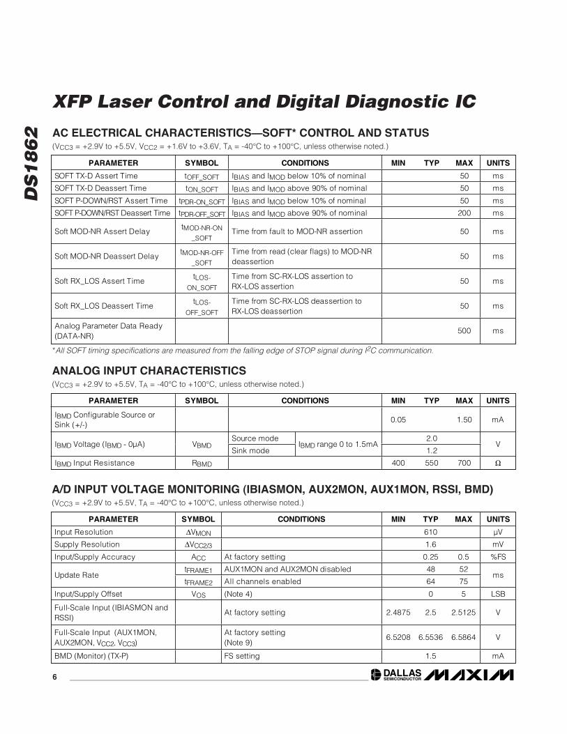
AC ELECTRICAL CHARACTERISTICS—SOFT* CONTROL AND STATUS(VCC3 = +2.9V to +5.5V, VCC2 = +1.6V to +3.6V, TA = -40°C to +100°C, unless otherwise noted.)
PARAMETER SYMBOL CONDITIONS MIN TYP MAX UNITS
SOFT TX-D Assert Time tOFF_SOFT IBIAS and IMOD below 10% of nominal 50 ms
SOFT TX-D Deassert Time tON_SOFT IBIAS and IMOD above 90% of nominal 50 ms
SOFT P-DOWN/RST Assert Time tPDR-ON_SOFT IBIAS and IMOD below 10% of nominal 50 ms
SOFT P-DOWN/RST Deassert Time tPDR-OFF_SOFT IBIAS and IMOD above 90% of nominal 200 ms
Soft MOD-NR Assert Delay tMOD-NR-ON
_SOFTTime from fault to MOD-NR assertion 50 ms
Soft MOD-NR Deassert Delay tMOD-NR-OFF
_SOFT
Time from read (clear flags) to MOD-NR deassertion
50 ms
Soft RX_LOS Assert Time tLOS-
ON_SOFT
Time from SC-RX-LOS assertion to RX-LOS assertion
50 ms
Soft RX_LOS Deassert Time tLOS-
OFF_SOFT
Time from SC-RX-LOS deassertion to RX-LOS deassertion
50 ms
Analog Parameter Data Ready (DATA-NR)
500 ms
*All SOFT timing specifications are measured from the falling edge of STOP signal during I2C communication.
ANALOG INPUT CHARACTERISTICS(VCC3 = +2.9V to +5.5V, TA = -40°C to +100°C, unless otherwise noted.)
PARAMETER SYMBOL CONDITIONS MIN TYP MAX UNITS
IBMD Configurable Source or Sink (+/-)
0.05 1.50 mA
Source mode 2.0 IBMD Voltage (IBMD - 0μA) VBMD
Sink mode IBMD range 0 to 1.5mA
1.2 V
IBMD Input Resistance RBMD 400 550 700
A/D INPUT VOLTAGE MONITORING (IBIASMON, AUX2MON, AUX1MON, RSSI, BMD)(VCC3 = +2.9V to +5.5V, TA = -40°C to +100°C, unless otherwise noted.)
PARAMETER SYMBOL CONDITIONS MIN TYP MAX UNITS
Input Resolution VMON 610 μV
Supply Resolution VCC2/3 1.6 mV
Input/Supply Accuracy ACC At factory setting 0.25 0.5 %FS
tFRAME1 AUX1MON and AUX2MON disabled 48 52 Update Rate
tFRAME2 All channels enabled 64 75 ms
Input/Supply Offset VOS (Note 4) 0 5 LSB
Full-Scale Input (IBIASMON and RSSI)
At factory setting 2.4875 2.5 2.5125 V
Full-Scale Input (AUX1MON, AUX2MON, VCC2, VCC3)
At factory setting (Note 9)
6.5208 6.5536 6.5864 V
BMD (Monitor) (TX-P) FS setting 1.5 mA
DS
18
62
XFP Laser Control and Digital Diagnostic IC
_____________________________________________________________________ 7
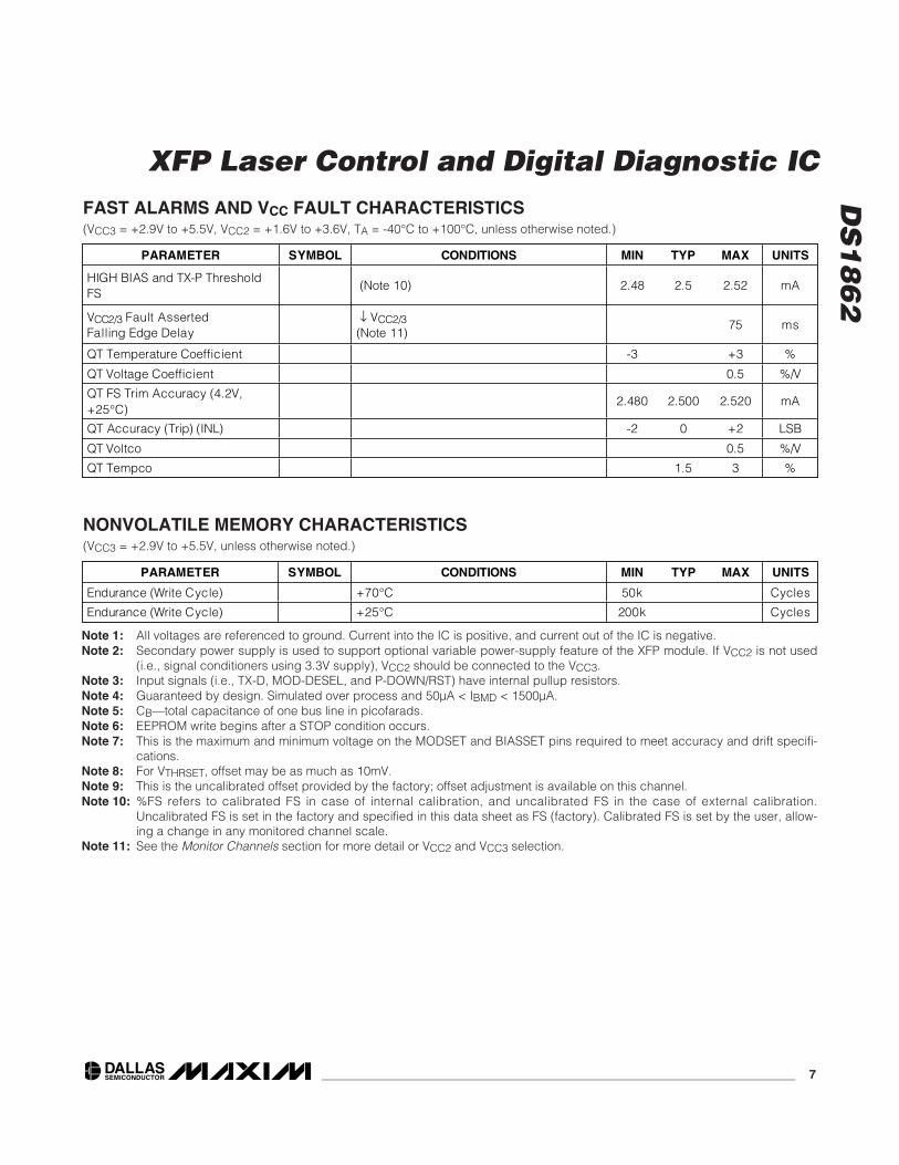
FAST ALARMS AND VCC FAULT CHARACTERISTICS(VCC3 = +2.9V to +5.5V, VCC2 = +1.6V to +3.6V, TA = -40°C to +100°C, unless otherwise noted.)
PARAMETER SYMBOL CONDITIONS MIN TYP MAX UNITS
HIGH BIAS and TX-P Threshold FS
(Note 10) 2.48 2.5 2.52 mA
VCC2/3 Fault Asserted Falling Edge Delay
VCC2/3(Note 11)
75 ms
QT Temperature Coefficient -3 +3 %
QT Voltage Coefficient 0.5 %/V
QT FS Trim Accuracy (4.2V, +25°C)
2.480 2.500 2.520 mA
QT Accuracy (Trip) (INL) -2 0 +2 LSB
QT Voltco 0.5 %/V
QT Tempco 1.5 3 %
Note 1: All voltages are referenced to ground. Current into the IC is positive, and current out of the IC is negative.Note 2: Secondary power supply is used to support optional variable power-supply feature of the XFP module. If VCC2 is not used
(i.e., signal conditioners using 3.3V supply), VCC2 should be connected to the VCC3.Note 3: Input signals (i.e., TX-D, MOD-DESEL, and P-DOWN/RST) have internal pullup resistors.Note 4: Guaranteed by design. Simulated over process and 50μA < IBMD < 1500μA.Note 5: CB—total capacitance of one bus line in picofarads.Note 6: EEPROM write begins after a STOP condition occurs.Note 7: This is the maximum and minimum voltage on the MODSET and BIASSET pins required to meet accuracy and drift specifi-
cations.Note 8: For VTHRSET, offset may be as much as 10mV.Note 9: This is the uncalibrated offset provided by the factory; offset adjustment is available on this channel.Note 10: %FS refers to calibrated FS in case of internal calibration, and uncalibrated FS in the case of external calibration.
Uncalibrated FS is set in the factory and specified in this data sheet as FS (factory). Calibrated FS is set by the user, allow-ing a change in any monitored channel scale.
Note 11: See the Monitor Channels section for more detail or VCC2 and VCC3 selection.
NONVOLATILE MEMORY CHARACTERISTICS(VCC3 = +2.9V to +5.5V, unless otherwise noted.)
PARAMETER SYMBOL CONDITIONS MIN TYP MAX UNITS
Endurance (Write Cycle) +70°C 50k Cycles
Endurance (Write Cycle) +25°C 200k Cycles

DS
18
62
XFP Laser Control and Digital Diagnostic IC
8 _____________________________________________________________________
Timing Diagrams
VCC > VPOA
TX-D
IBIASSET
IMODSET
tINIT
P-DOWN/RST
INTERRUPT
RESE
T-DO
NE
RESE
T-DO
NE
READ
-FLA
GS
tINIT_ON
tPDR-OFF
tINIT_OFFtINIT
READ
-FLA
GSFigure 1. Power-On Initialization with P-DOWN/RST Asserted and TX-D/SOFT TX-D Not Asserted
Figure 2. Power-On Initialization with P-DOWN/RST Not Asserted and TX-D/SOFT TX-D Not Asserted (Normal Operation)
VCC > VPOA
TX-D
IBIASSET
IMODSET
tINIT
P-DOWN/RST
INTERRUPT
tINIT_ON tINIT_OFF
READ
-FLA
GS
RESE
T-DO
NE

DS
18
62
XFP Laser Control and Digital Diagnostic IC
_____________________________________________________________________ 9
Timing Diagrams (continued)
TX-D
TX-F
IBIASSET
IMODSET
tOFF tON
Figure 3. TX-D Timing During Normal Operation
Figure 4. Detection of Safety Fault Condition
TX-D
FETG
OCCURRENCEOF FAULT
IBIASSET
IMODSET
tFAULT

DS
18
62
XFP Laser Control and Digital Diagnostic IC
10 ____________________________________________________________________
FETG
P-DOWN/RST
OCCURRENCEOF FAULT
IBIASSET
IMODSET
tRESET
tINIT
RESET-DONE
Figure 5. Successful Recovery from Transient Safety Fault Condition Using P-DOWN/RST
Figure 6. Unsuccessful Recovery from Transient Safety Fault Condition
FETG(FETG_POL = 1)
P-DOWN/RST
OCCURRENCEOF FAULT
IBIASSET
IMODSET
tRESET
tFAULT
tFAULT
RESE
T-DO
NE
Timing Diagrams (continued)

DS
18
62
XFP Laser Control and Digital Diagnostic IC
____________________________________________________________________ 11
READ FLAGS
OCCURRENCEOF MONITOR
CHANNEL FAULT tINIT_ON
tINIT_OFF
INTERRUPT
Figure 7. Monitor Channel Fault Timing
Timing Diagrams (continued)

DS
18
62
XFP Laser Control and Digital Diagnostic IC
12 ____________________________________________________________________
Typical Operating Characteristics(TA = +25°C, unless otherwise noted.)
SUPPLY CURRENT vs. SUPPLY VOLTAGE
DS18
62 to
c01
SUPPLY VOLTAGE (V)
SUPP
LY C
URRE
NT (m
A)
5.34.83.3 3.8 4.3
2.5
3.0
3.5
4.0
4.5
5.0
5.5
6.0
2.02.8
SRC_SINK_B = 1
SRC_SINK_B = 0
IBMD = 499.479μA
SUPPLY CURRENT vs. TEMPERATURE
DS18
62 to
c02
TEMPERATURE (°C)
SUPP
LY C
URRE
NT (m
A)
8560-15 10 353.0
3.5
4.0
4.5
5.0
5.5
6.0
-40
SRC_SINK_B = 1
SRC_SINK_B = 0
IBMD = 499.479μAVCC3 = 5.5V, VCC2 = 1.6V
IBMD DRIFT vs. TEMPERATURE
DS18
62 to
c03
TEMPERATURE (°C)
I BM
D DR
IFT
(%)
8560-15 10 35-2.5
-1.5
-2.0
-1.0
-0.5
0
0.5
1.0
-40
SRC_SINK_B = 1
SRC_SINK_B = 0
IBMD = 499.479μAVCC3 = 5.5V, VCC2 = 1.6V
IBMD DRIFT vs. SUPPLY VOLTAGE
DS18
62 to
c04
SUPPLY VOLTAGE (V)
I BM
D DR
IFT
(%)
5.23.6 4.4-1.0
0
-0.2
0.2
-0.6
-0.8
-0.4
0.4
0.6
0.8
1.0
2.8
SRC_SINK_B = 1
SRC_SINK_B = 0
IBMD = 499.479μA
IMODSET DRIFT vs. TEMPERATUREDS
1862
toc0
5
TEMPERATURE (°C)
I MOD
SET D
RIFT
(%)
85-15 10 35 60-2.0
-1.5
-1.0
-0.5
0
0.5
1.0
-40
IBMD = 499.479μAVCC3 = 5.5V, VCC2 = 1.6V
INTEGRAL NONLINEARITYOF QUICK TRIPS
DS18
62 to
c06
CODE (0–255)
ERRO
R (L
SB)
256128-0.8
-0.2
0
-0.6
-0.4
0.2
0.4
0.6
0.8
0
DIFFERENTIAL NONLINEARITYOF IMODSET
DS18
62 to
c07
CODE (0–255)
ERRO
R (L
SB)
256128-0.20
-0.05
0
-0.15
-0.10
0.05
0.10
0.15
0.20
0
FSR = 75μAVCC3 = 4.2V, VCC2 = 1.6V
INTEGRAL NONLINEARITYOF IMODSET
DS18
62 to
c08
CODE (0–255)
ERRO
R (L
SB)
256128-0.20
-0.05
0
-0.15
-0.10
0.05
0.10
0.15
0.20
0
FSR = 75μAVCC3 = 4.2V, VCC2 = 1.6V
DS
18
62
XFP Laser Control and Digital Diagnostic IC
____________________________________________________________________ 13
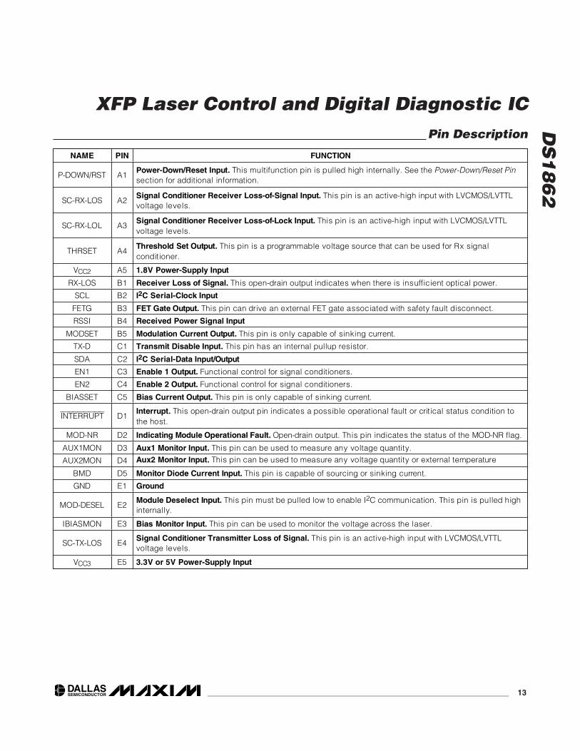
Pin Description
NAME PIN FUNCTION
P-DOWN/RST A1 Power-Down/Reset Input. This multifunction pin is pulled high internally. See the Power-Down/Reset Pinsection for additional information.
SC-RX-LOS A2 Signal Conditioner Receiver Loss-of-Signal Input. This pin is an active-high input with LVCMOS/LVTTL voltage levels.
SC-RX-LOL A3 Signal Conditioner Receiver Loss-of-Lock Input. This pin is an active-high input with LVCMOS/LVTTL voltage levels.
THRSET A4 Threshold Set Output. This pin is a programmable voltage source that can be used for Rx signal conditioner.
VCC2 A5 1.8V Power-Supply Input
RX-LOS B1 Receiver Loss of Signal. This open-drain output indicates when there is insufficient optical power.
SCL B2 I2C Serial-Clock Input
FETG B3 FET Gate Output. This pin can drive an external FET gate associated with safety fault disconnect.
RSSI B4 Received Power Signal Input
MODSET B5 Modulation Current Output. This pin is only capable of sinking current.
TX-D C1 Transmit Disable Input. This pin has an internal pullup resistor.
SDA C2 I2C Serial-Data Input/Output
EN1 C3 Enable 1 Output. Functional control for signal conditioners.
EN2 C4 Enable 2 Output. Functional control for signal conditioners.
BIASSET C5 Bias Current Output. This pin is only capable of sinking current.
INTERRUPT D1 Interrupt. This open-drain output pin indicates a possible operational fault or critical status condition to the host.
MOD-NR D2 Indicating Module Operational Fault. Open-drain output. This pin indicates the status of the MOD-NR flag.
AUX1MON D3 Aux1 Monitor Input. This pin can be used to measure any voltage quantity.
AUX2MON D4 Aux2 Monitor Input. This pin can be used to measure any voltage quantity or external temperature
BMD D5 Monitor Diode Current Input. This pin is capable of sourcing or sinking current.
GND E1 Ground
MOD-DESEL E2 Module Deselect Input. This pin must be pulled low to enable I2C communication. This pin is pulled high internally.
IBIASMON E3 Bias Monitor Input. This pin can be used to monitor the voltage across the laser.
SC-TX-LOS E4 Signal Conditioner Transmitter Loss of Signal. This pin is an active-high input with LVCMOS/LVTTL voltage levels.
VCC3 E5 3.3V or 5V Power-Supply Input
DS
18
62
XFP Laser Control and Digital Diagnostic IC
14 ____________________________________________________________________
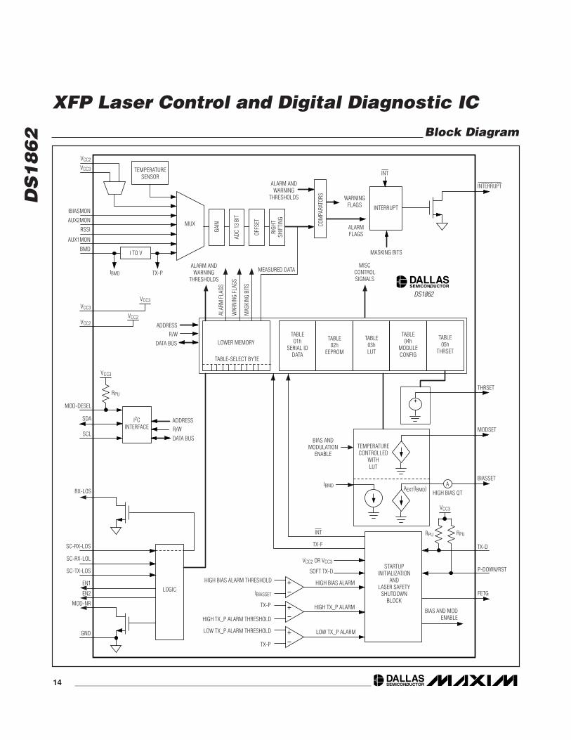
Block Diagram
MUX
VCC2
TX-P
LOGIC
SDA
SCL
MOD-DESEL
IBIASMON
RSSI
BMD
AUX1MON
ALARM ANDWARNING
THRESHOLDS
ALARM ANDWARNING
THRESHOLDS
INTERRUPT
WARNINGFLAGS
ALARMFLAGS
EN1
EN2
RX-LOS
SC-TX-LOS
SC-RX-LOL
SC-RX-LOS
VCC3
VCC2
VCC3
VCC2
AUX2MON
TX-PIBMD
TX-P
HIGH BIAS ALARM THRESHOLD
HIGH TX_P ALARM THRESHOLD
LOW TX_P ALARM THRESHOLD
IBIASSET
BIAS AND MODENABLE
TX-F
STARTUPINITIALIZATION
ANDLASER SAFETY
SHUTDOWNBLOCK
HIGH BIAS ALARM
HIGH TX_P ALARM
LOW TX_P ALARM
SOFT TX-D
VCC2 OR VCC3
P-DOWN/RST
TX-D
FETG
INT
GAIN
ALAR
M F
LAGS
WAR
NING
FLA
GS
MAS
KING
BIT
S
ADC
13 B
IT
OFFS
ET
RIGH
TSH
IFTI
NG
I2CINTERFACE
MEASURED DATA
COM
PARA
TORS
VCC3
VCC3
INTERRUPT
MOD-NR
GND
LOWER MEMORY
ADDRESSR/W
DATA BUS
ADDRESSR/W
DATA BUS
INT
TABLE-SELECT BYTE
TABLE01h
SERIAL IDDATA
TABLE02h
EEPROM
TABLE03hLUT
TABLE05h
THRSET
TABLE04h
MODULECONFIG
THRSET
MODSET
BIASSET
HIGH BIAS QTIBMD AEXT(IBMD)
BIAS ANDMODULATION
ENABLE
MASKING BITS
RPU
RPURPU
MISCCONTROLSIGNALS
TEMPERATURECONTROLLED
WITHLUT
TEMPERATURESENSOR
VCC3
I TO V
A
DS1862
DS
18
62
XFP Laser Control and Digital Diagnostic IC
____________________________________________________________________ 15
Detailed DescriptionThe DS1862’s block diagram is described in detailwithin the following sections and memory map/memorydescription.
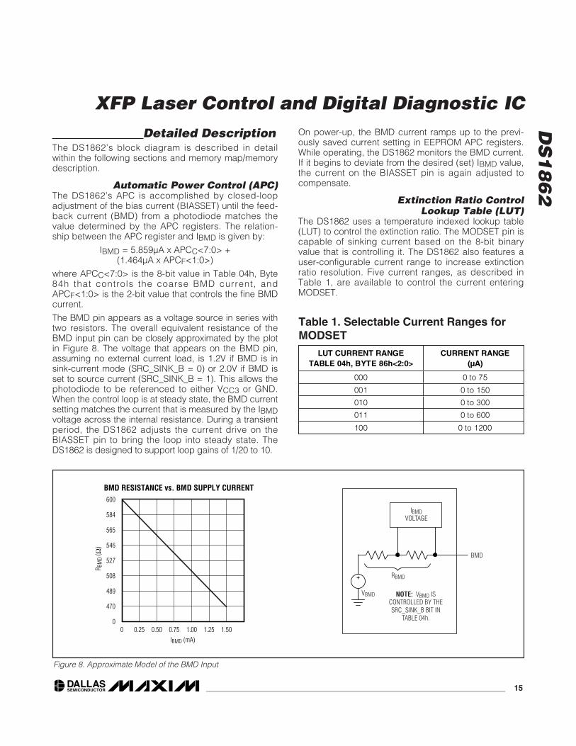
Automatic Power Control (APC)The DS1862’s APC is accomplished by closed-loopadjustment of the bias current (BIASSET) until the feed-back current (BMD) from a photodiode matches thevalue determined by the APC registers. The relation-ship between the APC register and IBMD is given by:
IBMD = 5.859μA x APCC<7:0> +(1.464μA x APCF<1:0>)
where APCC<7:0> is the 8-bit value in Table 04h, Byte84h that controls the coarse BMD current, andAPCF<1:0> is the 2-bit value that controls the fine BMDcurrent.
The BMD pin appears as a voltage source in series withtwo resistors. The overall equivalent resistance of theBMD input pin can be closely approximated by the plotin Figure 8. The voltage that appears on the BMD pin,assuming no external current load, is 1.2V if BMD is insink-current mode (SRC_SINK_B = 0) or 2.0V if BMD isset to source current (SRC_SINK_B = 1). This allows thephotodiode to be referenced to either VCC3 or GND.When the control loop is at steady state, the BMD currentsetting matches the current that is measured by the IBMDvoltage across the internal resistance. During a transientperiod, the DS1862 adjusts the current drive on theBIASSET pin to bring the loop into steady state. TheDS1862 is designed to support loop gains of 1/20 to 10.
On power-up, the BMD current ramps up to the previ-ously saved current setting in EEPROM APC registers.While operating, the DS1862 monitors the BMD current.If it begins to deviate from the desired (set) IBMD value,the current on the BIASSET pin is again adjusted tocompensate.
Extinction Ratio ControlLookup Table (LUT)
The DS1862 uses a temperature indexed lookup table(LUT) to control the extinction ratio. The MODSET pin iscapable of sinking current based on the 8-bit binaryvalue that is controlling it. The DS1862 also features auser-configurable current range to increase extinctionratio resolution. Five current ranges, as described inTable 1, are available to control the current enteringMODSET.
IBMDVOLTAGE
BMD
NOTE: VBMD ISCONTROLLED BY THESRC_SINK_B BIT IN
TABLE 04h.
IBMD (mA)
R BM
D (Ω
)
1.501.250.25 0.50 0.75 1.00
BMD RESISTANCE vs. BMD SUPPLY CURRENT
470
489
508
527
546
565
584
600
00
VBMD
RBMD
Figure 8. Approximate Model of the BMD Input
Table 1. Selectable Current Ranges forMODSET
LUT CURRENT RANGE TABLE 04h, BYTE 86h<2:0>
CURRENT RANGE (μA)
000 0 to 75
001 0 to 150
010 0 to 300
011 0 to 600
100 0 to 1200

DS
18
62
XFP Laser Control and Digital Diagnostic IC
16 ____________________________________________________________________
If the largest current range is selected, the maximumvalue of FFh (from LUT) corresponds to a 1200μA sinkcurrent. Regardless of the current range, the MODSETvalue always consists of 256 steps, including zero.
IMODSET can be controlled automatically with the tem-perature-based lookup table, or by three other manualmethods.
Automatic temperature addressed lookup is accom-plished by an internal or external temperature sensorcontrolling an address pointer. This pointer indexesthrough 127 previously loaded 8-bit current valuesstored in the LUT. Each one of the 127 temperatureslot locations corresponds to a 2°C increment overthe -40°C to +102°C temperature range. Any tempera-ture above or below these points causes the code inthe first or last temperature slot to be indexed. Both theinternal temperature sensor and an external sensorconnected to AUX2MON are capable of providing asignal to control the extinction ratio automatically withan indexed LUT. Table 2 illustrates the relationshipbetween the temperature and the memory locations inthe LUT.
Automatic and manual control of MODSET is controlledby two bits, TEN and AEN, that reside in Table 04h,Byte B2h. By default (from factory) TEN and AEN areboth set, causing complete automatic temperature-based lookup. If TEN and/or AEN are altered, theDS1862 is set to one of the manual modes. Table 3describes manual mode functionality.
Table 2. Temperature Lookup Table
TEMPERATURE (°C)CORRESPONDING LOOKUP
TABLE ADDRESS
< -40 80h
-40 80h
-38 81h
-36 82h
… …
+96 C4h
+98 C5h
+100 C6h
+102 C7h
> +102 C7h
Table 3. Truth Table for TEN and AEN Bits
TEN AEN DS1862 LUT FUNCTIONALITY
0 0
Manual mode that allows users to write a value directly to the LUT VALUE register (Table 04h, Byte B1h) to drive MODSET. While in this mode, the LUT INDEX POINTER register is not being updated, and no longer drives the LUT VALUE register.
0 1
Manual mode that allows users to write a value directly to the LUT VALUE register (Table 04h, Byte B1h) to drive MODSET. While in this mode, the LUT INDEX POINTER register is still being updated; however, it no longer drives the LUT VALUE register.
1 0
Manual mode that allows users to write a value to the LUT INDEX POINTER register (Table 04h, Byte B0), then the DS1862 updates the LUT VALUE register (Table 04h, Byte B1h) based on the user’s index pointer.
1 1
Automatic mode (factory default). This mode automatically indexes the LUT based on temperature, placing the resulting LUT address in the LUT INDEX POINTER register (Table 04h, Byte B0h). Then the MODSET setting is transferred from that LUT address to the LUT VALUE register (Table 04h, Byte B1h). Lastly, the IMODSET is set to the new MODSET code.

DS
18
62
XFP Laser Control and Digital Diagnostic IC
____________________________________________________________________ 17
Monitor ChannelsThe DS1862 has seven monitored voltage signals thatare polled in a round-robin multiplexed sequence andare updated with the frame rate, tFRAME. All channelsare read as 16-bit values, but have 13-bit resolution,and with the exception of temperature measurements,all channels are stored as unsigned values. The resulting16-bit value for all monitored channels, except internaltemperature, is calculated by internally averaging theanalog-to-digital result eight times. The resulting internaltemperature monitor channel is averaged 16 times. Seethe Internal Calibration section for a complete descrip-tion of each channel’s method(s) of internal calibration.
The AUX1MON, AUX2MON, and VCC2/3 monitor chan-nels are optional and can be disabled. This featureallows for shorter frame rate for the essential monitorchannels. Channels that cannot be disabled are inter-nal temperature, BMD, RSSI, and IBIASMON. A table offull-scale (FS) signal values (using factory internal cali-bration without right shifting) and the resulting FS codevalues for all seven channels is provided in Table 4.
Measuring Temperature—Internal or ExternalThe DS1862 is capable of measuring temperature onthree different monitor channels: internal temperaturesensor, AUX1MON, and AUX2MON. Only the internaltemperature and AUX2MON channels are capable ofindexing the LUT to control the extinction ratio. To usean external temperature sensor on AUX2MON, theTEMP_INT/EXT bit in Table 04h, Byte 8Bh, must be set.While AUX2MON controls the extinction ratio, the inter-nal temperature sensor does not stop running; despiteextinction ratio control by AUX2MON, it is this internaltemperature signal that continues to control the statusof temperature flags. Also, when TEMP_INT/EXT = 1,the internal temperature clamps at -40°C and+103.9375°C, and when TEMP_INT/EXT = 0 it clamps at -120°C and +127.984°C. AUX2MON, however, does haveits own flag to indicate an out-of-tolerance condition andassert the INTERRUPT pin.
Both AUX1MON and AUX2MON can be used to mea-sure temperature as a function of voltage on theirrespective pins. They can be enabled by selectingeither 0h or 4h from Table 5. Internal (or external) cali-bration may be required to transmute the input voltageto the desired two’s-complement digital code, readablefrom the result registers in lower memory, Bytes 6Ah,6Bh, 6Ch, 6Dh.
Measuring VCC2/3The DS1862 has the flexibility to internally measureeither VCC2 or VCC3 to monitor supply voltage. VCC2 orVCC3 is user selectable by the VCC2/3_SEL bit in Table01h, Byte DCh. To remove VCC2/3 from the round-robinmonitor update scheme, despite having VCC2 or VCC3selected to be monitored, the Reserve_EN bit in Table04h, Byte 8Bh can be programmed to a 0. The analogpower-on-reset flag, POA, indicates the status of VCC3power supply. Even though POA seems to behave simi-larly to VCC2/3 monitor channel, it is completely sepa-rate and has no connection.
Measuring APC and Laser Parameters—BMD,IBIASMON, RSSI
BMD and BIASSET are used to control and monitor thelaser functionality. Regardless of the set BMD current inthe APC register, the DS1862 measures BMD pin cur-rent and uses this value not only to adjust the currenton the BIASSET pin, but also to monitor TX-P as well.The IBIASMON pin is used to input a voltage signal tothe DS1862 that can be used to monitor the bias cur-rent through the laser. This monitor channel does notdrive the HIGH BIAS quick-trip (QT) alarms for safety
Table 4. Monitor Channel FS and LSB Detail
SIGNAL +FS SIGNAL +FS (hex) -FS SIGNAL -FS (hex) LSB
Temperature 127.984°C 7FF8 -120°C 8800 0.0625°C
VCC2/3 6.5528V FFF8 0V 0000 100μV
IBIASMON 2.4997V FFF8 0V 0000 38.147μV
RSSI 2.4997V FFF8 0V 0000 38.147μV
AUX1MON 6.5528V FFF8 0V 0000 38.147μV
AUX2MON 6.5528V FFF8 0V 0000 38.147μV
BMD (TX-P) 1.5mA FFF8 0mA 0000 22.888nA
RESERVE_EN VCC2/3_SEL RESULT
0 0 VCC2/3 result not enabled.
0 1 VCC2/3 result not enabled.
1 0 VCC3 is being measured.
1 1 VCC2 is being measured.

DS
18
62
XFP Laser Control and Digital Diagnostic IC
18 ____________________________________________________________________
fault functionality, current on the BIASSET pin is moni-tored by the DS1862 to control the HIGH BIAS quick-trip alarm. Similar to TX-P, the RSSI pin is used tomeasure the received power, RX-P.
Measuring Voltage Quantitiesusing AUX1MON and AUX2MON
AUX1MON and AUX2MON are auxiliary monitor inputsthat may be used to measure additional parameters.AUX1/2MON feature a user-selectable register thatdetermines the measured value’s units (i.e., voltage,current, or temperature). In addition to indicating units,some of the 4-bit op codes, in Table 5, also place thepart in special modes used for alarms and faults inter-nally. Whichever units’ scale is selected, the DS1862 isonly capable of measuring a positive voltage quantity,therefore internal or external calibration may be
required to get the binary value to match the measuredquantity. A table of acceptable units and/or their corre-sponding user-programmable 4-bit op code is provid-ed below.
Alarms and Warning FlagsBased on Monitor Channels
All of the monitor channels feature alarm and warningflags that are asserted automatically as user-pro-grammed thresholds are internally compared with mon-itor channel results. Flags may be set, which, if notmasked, will generate an interrupt on the INTERRUPTpin or generate a safety fault. Whenever VCC2/3,AUX2MON, AUX1MON, RSSI, and internal temperaturego beyond their threshold trip points and the corre-sponding mask bit is 0, an interrupt is generated on theINTERRUPT pin and a corresponding warning or alarmflag is set. Similarly, a safety fault occurs wheneverBMD or BIASSET go beyond threshold trip points.When this happens, the FETG pin immediately assertsand BIASSET and MODSET currents are shut down.
Monitor Channel Conversion ExampleTable 6 provides an example of how a 16-bit ADC codecorresponds to a real life measured voltage using thefactory-set calibration on either RSSI or IBIASMON. Byfactory default, the LSB is set to 38.147μV.
To calculate VCC2, VCC3, AUX1MON, or AUX2MON,convert the unsigned 16-bit value to decimal and multi-ply by 100μV.
To calculate the temperature (internal), treat the two’s-complement value binary number as an unsigned binary number, then convert it to decimal and divide by256. If the result is grater than or equal to 128, subtract256 from the result.
Temperature: high byte = -128°C to +127°C signed;low byte = 1/256°C.
Table 5. AUX1/2MON FunctionalitySelection (Unit Selection)
VALUEDESCRIPTION OF AUX1/2MON INTENDED USE
(UNITS OF MEASURE)
0000b Auxiliary monitoring not implemented
0001b APD bias voltage (16-bit value is voltage in units of 10mV)
0010b Reserved
0011b TEC current (mA) (16-bit value is current in units of 0.1mA)
0100b Laser temperature (same encoding as module temperature)
0101b Laser wavelength
0110b +5V supply voltage (encoded as primary voltage monitor)
0111b +3.3V supply voltage (encoded as primary voltage monitor)
1000b +1.8V supply voltage (encoded as primary voltage monitor) (VCC2)
1001b -5.2V supply voltage (encoded as primary voltage monitor)
1010b +5V supply current (16-bit value is current in 0.1mA)
1101b +3.3V supply current (16-bit value is current in 0.1mA)
1110b +1.8V supply current (16-bit value is current in 0.1mA)
1111b -5.2V supply current (16-bit value is current in 0.1mA)
Table 6. A/D Conversion Example
MSB (BIN) LSB (BIN) VOLTAGE (V)
11000000 00000000 1.875
10000000 10000000 1.255
Table 7. Temperature Bit Weights
S 26 25 24 23 22 21 20
2-1 2-2 2-3 2-4 2-5 — — —

DS
18
62
XFP Laser Control and Digital Diagnostic IC
____________________________________________________________________ 19
Internal CalibrationThe DS1862 has two means for scaling an analog inputto a digital result. The two devices alter the gain andoffset of the signal to be calibrated. All of the inputsexcept internal temperature have unique registers forboth the gain and the offset that can be found in Table04h. See the table below for a complete description ofinternal calibration capabilities including right-shiftingfor all monitor channels.
To scale a specific input’s gain and offset, the relation-ship between the analog input and the expected digitalresult must be known. The input that would produce acorresponding digital result of all zeroes is the nullvalue (normally this input is GND). The input that wouldproduce a corresponding digital result of all ones is thefull-scale (FS) value minus one LSB. The FS value isalso found by multiplying an all ones digital value bythe weighted LSB. For example, a digital reading is 16bits long, assume that the LSB is known to be 50μV,then the FS value would be 216 x 50μV = 3.2768V.
A binary search can be used to find the appropriategain value to achieve the desired FS of the converter.Once the gain value is determined, then it can be
loaded into the appropriate channels’ Gain register.This requires forcing two known voltages on to themonitor input pin. For best results, one of the forcedvoltages should be the NULL input and the othershould be 90% of FS. Since the LSB of the least signifi-cant byte in the digital reading register is known, theexpected digital results are also known for both the nulland FS value inputs. Figure 9 describes the hysteresisbuilt into the DS1862’s LUT functionality.
With the exception of BMD, which can source or sinkcurrent, all monitored channels are high impedanceand are only capable of directly measuring a voltage. Ifother measured quantities are desired, such as light,frequency, power, current, etc., they must be convertedto a voltage. In this situation the user is not interested involtage measurement on the monitored channel, butthe measurement of the desired parameter. Only therelationship between the indirect measured quantity(light, frequency, power, current, etc.) to the expecteddigital result must be known.
An example of gain scaling using the recommendedbinary search procedure is provided with the followingpseudo code.
To help will the computation, two integers need to bedefined: count 1 and count 2. CNT1 = NULL / LSB andCNT2 = 90%FS / LSB. CLAMP is the largest result thatcan be accommodated.
Table 8. Temperature ConversionExamples
MSB (BIN) LSB (BIN) TEMPERATURE (°C)
01000000 00000000 +64
01000000 00001000 +64.03215
01011111 00000000 +95
11110110 00000000 -10
11011000 00000000 -40
Table 9. Internal Calibration Capabilities
SIGNALINTERNAL SCALING
INTERNAL OFFSET
RIGHT- SHIFTING
Temperature — x —
VCC2/3 x x —
IBIASMON x x x
RSSI (RX-P) x x x
AUX1MON x x x
AUX2MON x x x
BMD (TX-P) x x x
M6
M5
M4
M3
M2
M1
2 4 6 8 10 12TEMPERATURE (°C)
MEM
ORY
LOCA
TION
INCREASING TEMPERATURE
DECREASING TEMPERATURE
Figure 9. Lookup Table Hysteresis

DS
18
62
XFP Laser Control and Digital Diagnostic IC
20 ____________________________________________________________________
/* Assume that the Null input is 0.5V. */
/* In addition, the requirement for LSB is 50μV. */
FS = 65536 * 50e-6; /* 3.2768 */
CNT1 = 0.5 / 50e-6; /* 10000 */
CNT2 = 0.90*FS / 50e-6; /* 58982 */
/* Thus the NULL input of 0.5V and the 90% of FS inputis 2.94912V. */
set the trim-offset-register to zero;
set Right-Shift register to zero (Typically zero. See the Right-Shifting section);
gain_result = 0h;
CLAMP = FFF8h/2^(Right_Shift_Register);
For n = 15 down to 0
begin
gain_result = gain_result + 2^n;
Force the 90% FS input (2.94912V);
Meas2 = read the digital result from the part;
If Meas2 >= CLAMP then
gain_result = gain_result - 2^n;
Else
Force the NULL input (0.5V);
Meas1 = read the digital result from the part;
if (Meas2 - Meas1) > (CNT2 - CNT1) then
gain_result = gain_result - 2^n;
end;
Set the gain register to gain_result;
The gain register is now set and the resolution of theconversion will best match the expected LSB. The nextstep is to calibrate the offset of the DS1862. With thecorrect gain value written to the gain register, againforce the NULL input to the monitor pin. Read the digi-tal result from the part (Meas1). The offset value isequal to negative value of Meas1.
The calculated offset is now written to the DS1862 andthe gain and offset-scaling procedure is complete.
Right-Shifting A/D Conversion Result(Scalable Dynamic Ranging)
Right-shifting is a digital method used to regain someof the lost ADC range of a calibrated system. If right-shifting is enabled, by simply loading a non-zero valueinto the appropriate Right-Shifting Register, then theDS1862 shifts the calibrated result just before it isstored into the monitor channels’ register. If a system iscalibrated so the maximum expected input results in adigital output value of less than 7FFFh (50% of FS),then it is a candidate for using the right-shiftingmethod.
If the maximum desired digital output is less than7FFFh, then the calibrated system is using less than 1/2the ADC’s range. Similarly, if the maximum desired dig-ital output is less than 1FFFh, then the calibrated sys-tem is only using 1/8th the ADC’s range. For example, ifan applied maximum analog signal yields a maximumdigital output less than 1FFCh, then only 1/8th of theADC’s range is used. Right-shifting improves the reso-lution of the measured signal as part of internal calibra-tion. Without right-shifting, the 3 MS bits of the ADC willnever be used. In this example, a value of 3 for theright-shifting maximizes the ADC range and a largergain setting must be loaded to achieve optimal conver-sion. No resolution is lost since this is a 13-bit converterthat is left justified. The value can be right-shifted 3times without losing any resolution. The following tabledescribes when the right-shifting method can be effec-tively used.
OFFSET REGISTERMeas
_( )= −⎡
⎣⎢⎤⎦⎥
1 14
Table 10. Right-Shifting Selection
OUTPUT RANGE USED WITH ZERO RIGHT-SHIFTS
NUMBER OF RIGHT-SHIFTS NEEDED
0h .. FFFFh 0
0h .. 7FFFh 1
0h .. 3FFFh 2
0h .. 1FFFh 3
0h .. 0FFFh 4

DS
18
62
XFP Laser Control and Digital Diagnostic IC
____________________________________________________________________ 21
Warning and Alarm Logic Based onAUX1/2MON, VCC2/3, Temp, RX-P,
and IBIASMONThe DS1862 is capable of generating an alarm and/orwarning whenever an analog monitored channel goesout of a user-defined tolerance. Temperature, bias cur-rent (based on IBIASMON), receive power (based onRSSI), AUX1MON, AUX2MON, and VCC2/3, are moni-
tored channels that generate latched flags. See the fig-ure below for more detail pertaining to AUX1MON andAUX2MON. Flags are latched into a high state the firsttime a monitored channel goes out of the defined oper-ating window and for each monitored signal there is aMask bit that can be set to prevent the correspondingalarm or warning flag from being set. Once a flag is set,it is cleared by simply reading its memory location.
AUX1/2MON LOGIC
AUX1MON (PIN)
AUX2MON (PIN)
MASK BIT
AUX1MON
AUX2MON
ADC
THRESHOLD
AUX1MON(APD MODE) LATCHED-APD-
SUPPLY-FAULTAUX2MON
(APD MODE)
INTERRUPT (PIN)
*COMPARATOR LOGIC ISDUPLICATED FOR HIGHAND LOW ALARMS AND
WARNINGS.
C
ADC
THRESHOLDC
4-BI
T UN
IT S
ELEC
T
LATC
H
AUX1MON(LASER WL MODE) LATCHED-
WAVELENGTH-ULAUX2MON
(LASER WL MODE)
LATC
H
AUX1MON(VEE5 MODE)
LATCHED-VEE5AUX2MON
(VEE5 MODE)
LATC
H
AUX1MON(VCC2 MODE)
LATCHED-VCC2AUX2MON
(VCC2 MODE)
LATC
H
AUX1MON(TEC MODE) LATCHED-TEC-
FAULTAUX2MON
(TEC MODE)
LATC
H
AUX1MON(VCC5 MODE)
LATCHED-VCC5AUX2MON
(VCC5 MODE)
LATC
H
AUX1MON(VCC3 MODE)
LATCHED-VCC3AUX2MON
(VCC3 MODE)
LATC
H
ANY FLAG
CORRESPONDING MASKBIT
*
*
Figure 10. AUX1/2MON Monitor Logic

DS
18
62
XFP Laser Control and Digital Diagnostic IC
22 ____________________________________________________________________
Warning and Alarm Logic Based onSignal Conditioners
The DS1862 also has flags that are set by certain logicalconditions on signal conditioner (SC) pins: SC-RX-LOL,SC-RX-LOS, SC-TX-LOS. Similarly, for each latchedsignal conditioner flag there are also mask bits that arecapable of preventing the alarm or warning flag fromcausing an INTERRUPT pin to assert. Again, flags arecleared automatically whenever their memory addressis read. See Figure 11 for more detail.
Quick-Trip Logic and FETGShutdown Functionality
In addition to alarms and warnings, the DS1862 alsohas quick-trip (QT) functionality (sometimes referred to
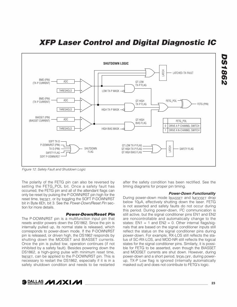
as fast alarms) that is capable of shutting down theLASER with the FETG pin in conjunction with shuttingdown IMODSET and IBIASSET. IBMD and IBIASSET cur-rents are measured and are compared with user-defined trip points to set the quick-trip flags: QT LOWTX-P, QT HIGH TX-P, and QT HIGH BIAS. These flagsare also capable of being masked to prevent FETGfrom being asserted when an out-of-tolerance conditionis detected. FETG is not asserted by setting the TX-Dpin, SOFT TX-D, or P-DOWN/RST pin to a high state,however, IMODSET, and IBIASSET will shut down. SeeFigure 12 for more detail.
SIGNAL CONDITIONER AND MISCELLANEOUS LOGIC
ANY FLAG
ANY MASK BIT
HIGH TX-PLOW TX-P LATCHED-TX-FAULTHIGH BIAS
INTERRUPT (PIN)
TIMER
LATC
H
SC-RX-LOS(PIN)
LATCHED-RX-NRSC-RX-LOL
(PIN)
LATC
H
SC-TX-LOS(PIN)
LATCHED-TX-NRLATCHED-TX-FAULT LA
TCH
P-DOWN/RST(PIN)
LATCHED-RESET-DONE
LATCHEDRX-CDR-NL
LATC
HLA
TCH
SC-RX-LOL(PIN)
LATCHED-RX-LOS RX-LOS (PIN)
*
*
LATC
H
SC-RX-LOS(PIN)
SC-RX-LOL (PIN)TX-FAULT
LATCHED-MOD-NR
VCC2-FAULT
*OPEN DRAIN
MOD-NR (PIN)
LATC
H
Figure 11. Signal Conditioner and Other Logic
DS
18
62
XFP Laser Control and Digital Diagnostic IC
____________________________________________________________________ 23
The polarity of the FETG pin can also be reversed bysetting the FETG_POL bit. Once a safety fault hasoccurred, the FETG pin and all of the attendant flags canonly be reset by pulsing the P-DOWN/RST pin high for thereset time, tRESET, or by toggling the SOFT P-DOWN/RSTbit in Byte 6Eh, bit 3. See the Power-Down/Reset Pin sec-tion for more details.
Power-Down/Reset PinThe P-DOWN/RST pin is a multifunction input pin thatresets and/or powers down the DS1862. Since the pin isinternally pulled up, its normal state is released, whichcorresponds to power-down mode. If the P-DOWN/RSTpin is released, or driven high, the DS1862 responds byshutting down the MODSET and BIASSET currents.Once the pin is pulled low, operation continues (if notinhibited by a safety fault). Besides powering down theDS1862, a high-going pulse with minimum reset time,tRESET, can be applied to the P-DOWN/RST pin. This isnecessary to restart the DS1862, especially if it is in asafety shutdown condition and needs to be restarted
after the safety condition has been rectified. See thetiming diagrams for proper pin timing.
Power-Down FunctionalityDuring power-down mode IBIASSET and IMODSET dropbelow 10μA, effectively shutting down the laser. FETGis not asserted and safety faults do not occur duringthis period. During power-down, I2C communication isstill active, but the signal conditioner pins EN1 and EN2are noncontrollable and automatically change to thestates: EN1 = 1 and EN2 = 0. Other internal flags/sig-nals that are based on the signal conditioner inputs stillreflect the status on the signal conditioner pins duringpower-down. For example, RX-LOS still reflects the sta-tus of SC-RX-LOS, and MOD-NR still reflects the logicalstates for the signal conditioner pins. Similarly, it is possi-ble for FETG to be asserted, even though the BIASSETand MODSET currents are shut down. However, duringpower-down and a short period, tPDR-OFF, during power-up, TX-P Low flag is ignored (internally automaticallymasked out) and does not contribute to FETG’s logic.
SHUTDOWN LOGIC
BMD (PIN)(TX-P CURRENT)
BMD (PIN)(TX-P CURRENT)
LOW TX-P MASK
HIGH TX-P MASK
QT LOWTX-P FLAG
QT HIGHTX-P FLAG
ADC
THRESHOLD
ADC
THRESHOLD
HIGH BIAS MASK
QT HIGHBIAS FLAG
BIASSET (PIN)(BIASSET CURRENT) ADC
THRESHOLD
SOFT TX-DP-DOWN/RST (PIN)
TX-D (PIN) SHUTDOWNFLAGSAFETY FLAG
SOFT P-DOWN/RST
QT LOW TX-P FLAGQT HIGH TX-P FLAG SAFETY FLAG
FETG_POL
DRIVE A P-CHANNEL SWITCH
DRIVE A N-CHANNEL SWITCH
0
1
QT HIGH BIAS FLAG LATC
H
LATCHED-TX-FAULT
LATC
H
FETG (PIN)FETG_POL
Figure 12. Safety Fault and Shutdown Logic
DS
18
62
XFP Laser Control and Digital Diagnostic IC
24 ____________________________________________________________________
During an asserted period of P-DOWN/RST (DS1862 inpower-down), and VCC3 is cycled, the DS1862 remainsin power-down mode upon power-up. While in power-down mode the INTERRUPT pin does not assert. OnceVCC3 has returned, the reset done flag asserts after theinterrupt assert delay, tINIT_ON.
Reset FunctionalityBesides powering down the DS1862, the P-DOWN/RSTpin also functions to reset the DS1862. After a high-going pulse of time tRESET, several events occur withinthe DS1862. First, MODSET and BIASSET currents shutdown and are then reinstated. Second, between the ris-ing edge of the reset pulse and the assertion of thereset-done flag (tINIT), the low TX-P flag is ignored anddoes not cause FETG to trip. After time tINIT, the lowTX-P flag becomes functional. Also, at this time, thereset-done flag is asserted, causing an interrupt to begenerated. If there are no faults before tINIT, then nointerrupts are asserted on the INTERRUPT pin.
If VCC3 is powered up while P-DOWN/RST is high, thenthe reset-done flag must be cleared twice. The first timethe reset-done flag is generated by VCC3 powering up,the second time reset-done is generated by a fallingedge on P-DOWN/RST. If VCC3 is continuously pow-ered while P-DOWN/RST is low then only one reset-done flag needs to be cleared. See the timingdiagrams for graphical detail.
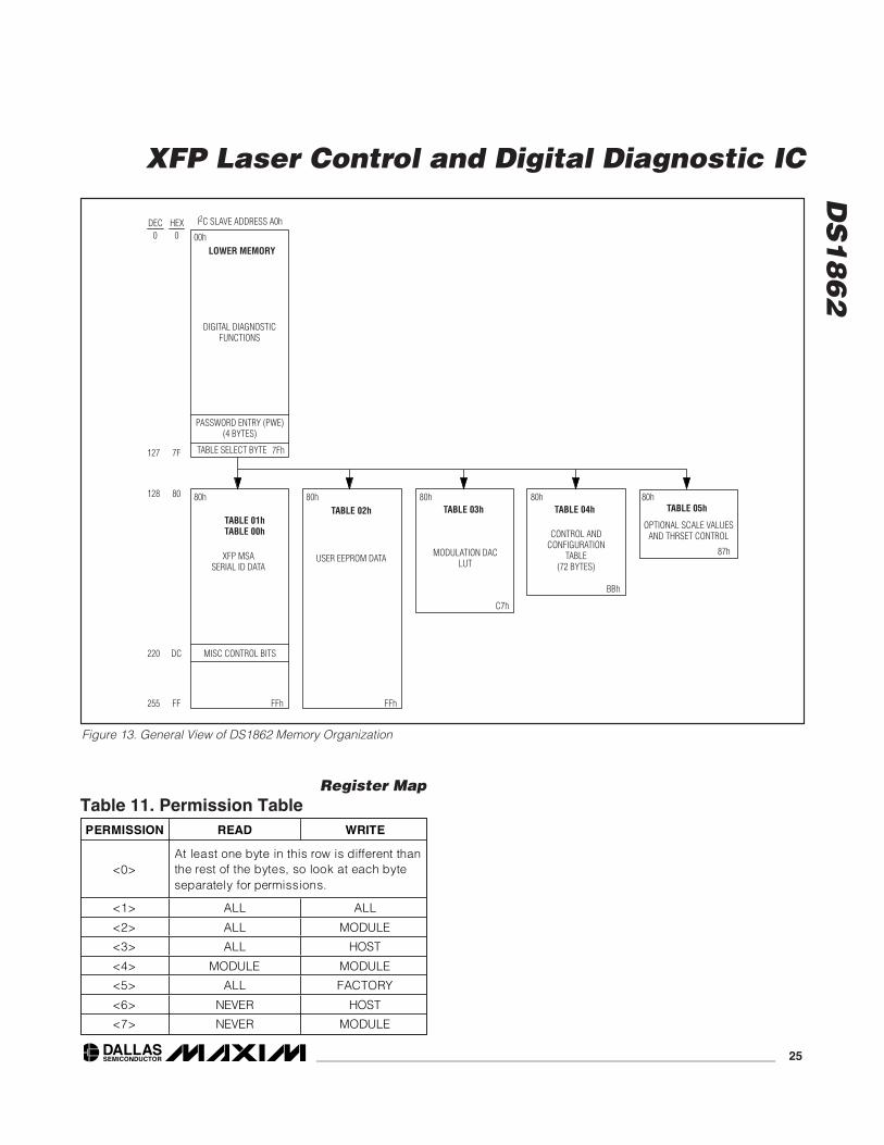
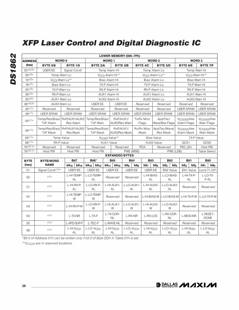
Memory MapMemory Organization
The DS1862 features six separate memory tables thatare internally organized into 4-word rows. The LowerMemory is addressed from 00h to 7Fh and containsalarm and warning thresholds, flags, masks, severalcontrol registers, password entry area (PE), and the
table select byte. Table 01h primarily contains userEEPROM as well as several control bytes for variousfunctions. Table 02h is strictly user EEPROM that is pro-tected by a host password. Table 03h is strictly usedfor controlling the extinction ratio with an LUT. Table04h is a multifunction space that contains internal cali-bration values for monitored channels, LUT index point-ers, and miscellaneous control bytes. Table 05h isfactory programmed and stores SCALE values for usewith suggested external temperature sensors. Also, onebyte in Table 05h controls the THRSET voltage sourceand is completely accessible without any passwordprotection. See the Detailed Register Description sec-tion for a more complete detail of each byte’s function,as well as Table 11 for read/write permissions for eachbyte. Many nonvolatile memory locations are actuallySRAM-shadowed EEPROM, which are controlled by theSEEB bit in Table 04h, Byte B2h.
The DS1862 incorporates SRAM-shadowed EEPROMmemory locations for key memory addresses that maybe rewritten many times. By default the shadowed-EEPROM bit, SEEB, is not set and these locations actas ordinary EEPROM. By setting SEEB, these loca-tions begin to function like SRAM cells, which allow aninfinite number of write cycles without concern of wear-ing out the EEPROM. This also eliminates the require-ment for the EEPROM write t ime, tWR. Becausechanges made with SEEB enabled do not affect theEEPROM, these changes are not retained throughpower cycles. The power-up value is the last value writ-ten with SEEB disabled. This function can be used tolimit the number of EEPROM writes during calibration orto change the monitor thresholds periodically duringnormal operation helping to reduce the number of timesEEPROM is written. The following information describeswhich locations are shadowed-EEPROM.
DS
18
62
XFP Laser Control and Digital Diagnostic IC
____________________________________________________________________ 25
DEC HEX0 0
I2C SLAVE ADDRESS A0h
127 7F
128 80
TABLE SELECT BYTE
255 FF
TABLE 01hTABLE 00h
TABLE 02h TABLE 04hTABLE 03h80h
C7h
CONTROL ANDCONFIGURATION
TABLE(72 BYTES)
MODULATION DACLUTUSER EEPROM DATA
80h 80h80h
BBh
FFh
XFP MSASERIAL ID DATA
PASSWORD ENTRY (PWE)(4 BYTES)
00h
7Fh
LOWER MEMORY
DIGITAL DIAGNOSTICFUNCTIONS
TABLE 05h
OPTIONAL SCALE VALUESAND THRSET CONTROL
80h
87h
FFh
DC220 MISC CONTROL BITS
Figure 13. General View of DS1862 Memory Organization
Register MapTable 11. Permission TablePERMISSION READ WRITE
<0>At least one byte in this row is different than the rest of the bytes, so look at each byte separately for permissions.
<1> ALL ALL
<2> ALL MODULE
<3> ALL HOST
<4> MODULE MODULE
<5> ALL FACTORY
<6> NEVER HOST
<7> NEVER MODULE
DS
18
62
XFP Laser Control and Digital Diagnostic IC
26 ____________________________________________________________________
LOWER MEMORY (00h–7Fh)
WORD 0 WORD 1 WORD 2 WORD 3 ADDRESS (hex) BYTE 0/8 BYTE 1/9 BYTE 2/A BYTE 3/B BYTE 4/C BYTE 5/D BYTE 6/E BYTE 7/F
00<0,2> USER EE Signal Cond* Temp Alarm Hi Temp Alarm Lo Temp Warn Hi
08<2> Temp Warn Lo VCC3 Alarm Hi** VCC3 Alarm Lo** VCC3 Warn Hi**
10<2> VCC3 Warn Lo** Bias Alarm Hi Bias Alarm Lo Bias Warn Hi
18<2> Bias Warn Lo TX-P Alarm Hi TX-P Alarm Lo TX-P Warn Hi
20<2> TX-P Warn Lo RX-P Alarm Hi RX-P Alarm Lo RX-P Warn Hi
28<2> RX-P Warn Lo AUX1 Alarm Hi AUX1 Alarm Lo AUX1 Warn Hi
30<2> AUX1 Warn Lo AUX2 Alarm Hi AUX2 Alarm Lo AUX2 Warn Hi
38<0,2> AUX2 Warn Lo USER EE USER EE Reserved Reserved Reserved Reserved
40<1> Reserved Reserved Reserved Reserved Reserved Reserved USER SRAM USER SRAM
48<1> USER SRAM USER SRAM USER SRAM USER SRAM USER SRAM USER SRAM USER SRAM USER SRAM
50<1> Temp/Res/Bias/ TxP Alarm
RxP/AUX1/AUX2/ Res Alarm
Temp/Res/Bias/ TxP Warn
RxP/AUX1/ AUX2/Res Warn
Tx/Rx Misc Flags
Apd/Tec/ Wave/Res Flags
VCC5/3/2/Vee Alarm Flags
VCC5/3/2/Vee Warn Flags
58<1> Temp/Res/Bias/ TxP Mask
RxP/AUX1/AUX2/ Res Mask
Temp/Res/Bias/ TxP Mask
RxP/AUX1/ AUX2/Res Mask
Rx/Rx Misc Mask
Apd/Tec/Wave/ Res Mask
VCC5/3/2/Vee Alarm Mask
VCC5/3/2/Vee Warn Mask
60<1> Temp Value VCC2/3 Value** Bias Value TX-P Value
68<1> RX-P Value AUX1 Value AUX2 Value GCS1 GCS0 70<0,1> Reserved Reserved Reserved Reserved POA Reserved PEC_EN Host PW 78<0,1> Host PW Host PW Host PW PWE (MSB) PWE (LSB) Table Select
EXPANDED BYTES
Bit7 Bit6* Bit5 Bit4 Bit3 Bit2 Bit1 Bit0 BYTE (hex)
BYTE/WORD NAME bit15 bit14 bit13 bit12 bit11 bit10 bit9 bit8 bit7 bit6 bit5 bit4 bit3 bit2 bit1 bit0
01 Signal Cond<1>* USER EE USER EE USER EE USER EE USER EE EN2 Value EN1 Value Lock-T1-221
50 <1> L-HI-TEMP-AL
L-LO-TEMP-AL
Reserved ReservedL-HI-BIAS-
AL L-LO-BIAS-
AL L-HI-TX-P-
AL L-LO-TX-
P-AL
51 <1> L-HI-RX-P- AL
L-LO-RX-P- AL
L-HI-AUX1-AL
L-LO-AUX1-AL
L-HI-AUX2-AL
L-LO-AUX2-AL
Reserved Reserved
52 <1> L-HI-TEMP- W
L-LO-TEMP- W
Reserved Reserved L-HI-BIAS-W L-LO-BIAS-W L-HI-TX-P-W L-LO-TX-P-W
53 <1> L-HI-RX-P-W L-LO-RX-P-
WL-HI-AUX1-
WL-LO-AUX1-
WL-HI-AUX2-
WL-LO-AUX2-
WReserved Reserved
54 <1> L-TX-NR L-TX-F L-TX-CDR-
NL L-RX-NR L-RX-LOS
L-RX-CDR- NL
L-MOD-NR L-RESET-
DONE
55 <1> L-APD-SUP-F L-TEC-F L-WAVE-NL Reserved Reserved Reserved Reserved Reserved
56 <1> L-HI-VCC5-AL
L-LO–VCC5-AL
L-HI-VCC3-AL
L-LO–VCC3-AL
L-HI-VCC2-AL
L-LO–VCC2-AL
L-HI-VEE5-AL
L-LO-VEE5-AL
*Bit 0 of Address 01h can be written only if bit 0 of Byte DDh in Table 01h is set.
**VCC2/3 are in reserved locations.
DS
18
62
XFP Laser Control and Digital Diagnostic IC
____________________________________________________________________ 27
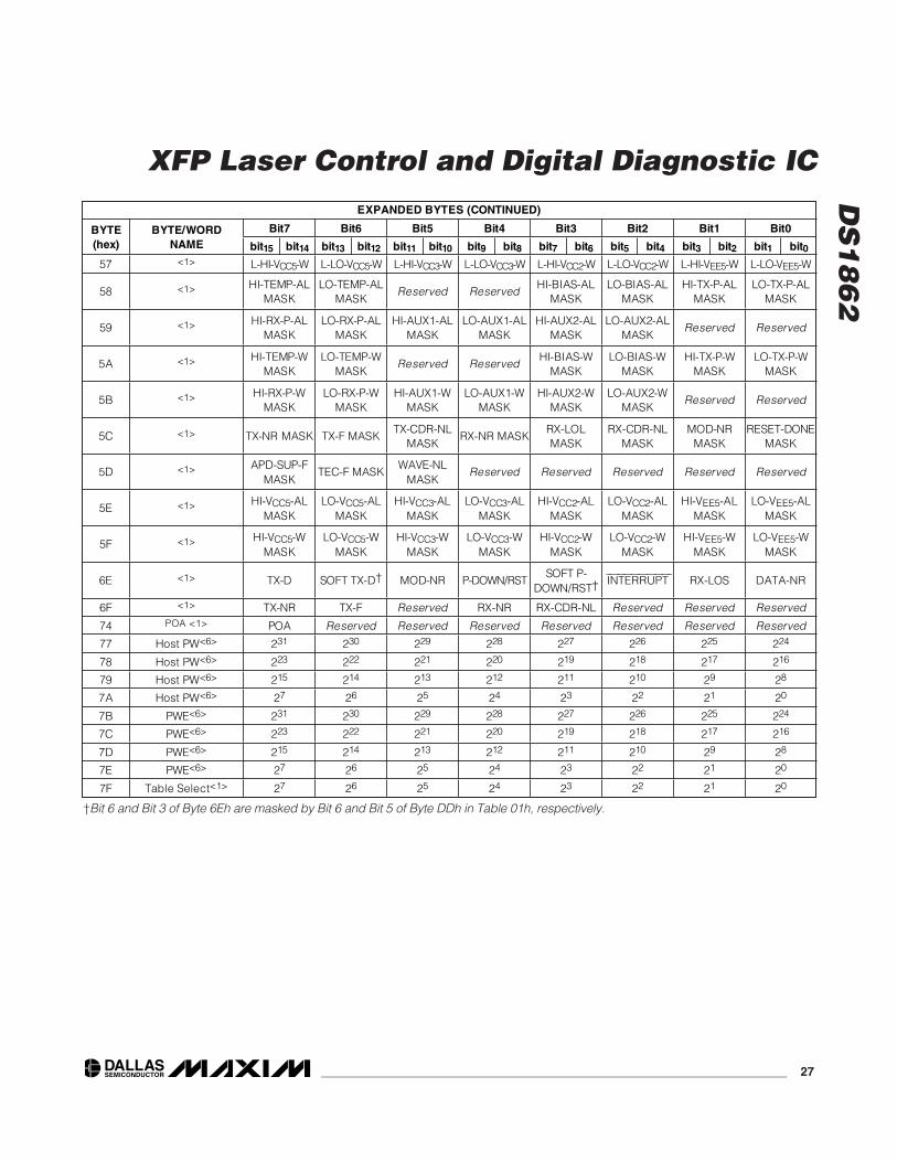
EXPANDED BYTES (CONTINUED)
Bit7 Bit6 Bit5 Bit4 Bit3 Bit2 Bit1 Bit0 BYTE (hex)
BYTE/WORD NAME bit15 bit14 bit13 bit12 bit11 bit10 bit9 bit8 bit7 bit6 bit5 bit4 bit3 bit2 bit1 bit0
57 <1> L-HI-VCC5-W L-LO-VCC5-W L-HI-VCC3-W L-LO-VCC3-W L-HI-VCC2-W L-LO-VCC2-W L-HI-VEE5-W L-LO-VEE5-W
58 <1> HI-TEMP-AL MASK
LO-TEMP-AL MASK
Reserved ReservedHI-BIAS-AL
MASK LO-BIAS-AL
MASK HI-TX-P-AL
MASK LO-TX-P-AL
MASK
59 <1> HI-RX-P-AL MASK
LO-RX-P-AL MASK
HI-AUX1-AL MASK
LO-AUX1-AL MASK
HI-AUX2-AL MASK
LO-AUX2-AL MASK
Reserved Reserved
5A <1> HI-TEMP-W MASK
LO-TEMP-W MASK
Reserved ReservedHI-BIAS-W
MASK LO-BIAS-W
MASK HI-TX-P-W
MASK LO-TX-P-W
MASK
5B <1> HI-RX-P-W MASK
LO-RX-P-W MASK
HI-AUX1-W MASK
LO-AUX1-W MASK
HI-AUX2-W MASK
LO-AUX2-W MASK
Reserved Reserved
5C <1> TX-NR MASK TX-F MASK TX-CDR-NL
MASK RX-NR MASK
RX-LOL MASK
RX-CDR-NL MASK
MOD-NR MASK
RESET-DONE MASK
5D <1> APD-SUP-F MASK
TEC-F MASK WAVE-NL
MASK Reserved Reserved Reserved Reserved Reserved
5E <1> HI-VCC5-AL MASK
LO-VCC5-AL MASK
HI-VCC3-AL MASK
LO-VCC3-AL MASK
HI-VCC2-AL MASK
LO-VCC2-AL MASK
HI-VEE5-AL MASK
LO-VEE5-AL MASK
5F <1> HI-VCC5-W MASK
LO-VCC5-WMASK
HI-VCC3-W MASK
LO-VCC3-WMASK
HI-VCC2-W MASK
LO-VCC2-WMASK
HI-VEE5-W MASK
LO-VEE5-W MASK
6E <1> TX-D SOFT TX-D† MOD-NR P-DOWN/RST SOFT P-
DOWN/RST† INTERRUPT RX-LOS DATA-NR
6F <1> TX-NR TX-F Reserved RX-NR RX-CDR-NL Reserved Reserved Reserved
74 POA <1> POA Reserved Reserved Reserved Reserved Reserved Reserved Reserved
77 Host PW<6> 231 230 229 228 227 226 225 224
78 Host PW<6> 223 222 221 220 219 218 217 216
79 Host PW<6> 215 214 213 212 211 210 29 28
7A Host PW<6> 27 26 25 24 23 22 21 20
7B PWE<6> 231 230 229 228 227 226 225 224
7C PWE<6> 223 222 221 220 219 218 217 216
7D PWE<6> 215 214 213 212 211 210 29 28
7E PWE<6> 27 26 25 24 23 22 21 20
7F Table Select<1> 27 26 25 24 23 22 21 20
†Bit 6 and Bit 3 of Byte 6Eh are masked by Bit 6 and Bit 5 of Byte DDh in Table 01h, respectively.
DS
18
62
XFP Laser Control and Digital Diagnostic IC
28 ____________________________________________________________________
TABLE 01h (SERIAL ID MEMORY)
WORD 0 WORD 1 WORD 2 WORD 3 ADDRESS (hex) Byte 0/8 Byte 1/9 Byte 2/A Byte 3/B Byte 4/C Byte 5/D Byte 6/E Byte 7/F
80<2> USER EE USER EE USER EE USER EE USER EE USER EE USER EE USER EE
88<2> USER EE USER EE USER EE USER EE USER EE USER EE USER EE USER EE
90<2> USER EE USER EE USER EE USER EE USER EE USER EE USER EE USER EE
98<2> USER EE USER EE USER EE USER EE USER EE USER EE USER EE USER EE
A0<2> USER EE USER EE USER EE USER EE USER EE USER EE USER EE USER EE
A8<2> USER EE USER EE USER EE USER EE USER EE USER EE USER EE USER EE
B0<2> USER EE USER EE USER EE USER EE USER EE USER EE USER EE USER EE
B8<2> USER EE USER EE USER EE USER EE USER EE USER EE USER EE USER EE
C0<2> USER EE USER EE USER EE USER EE USER EE USER EE USER EE USER EE
C8<2> USER EE USER EE USER EE USER EE USER EE USER EE USER EE USER EE
D0<2> USER EE USER EE USER EE USER EE USER EE USER EE USER EE USER EE
D8<2> USER EE USER EE USER EE USER EE VCC2/3_SEL LO MEM 6Eh
EN AUX1/2 UNIT
SEL USER EE
E0<2> USER EE USER EE USER EE USER EE USER EE USER EE USER EE USER EE
E8<2> USER EE USER EE USER EE USER EE USER EE USER EE USER EE USER EE
F0<2> USER EE USER EE USER EE USER EE USER EE USER EE USER EE USER EE
F8<2> USER EE USER EE USER EE USER EE USER EE USER EE USER EE USER EE
EXPANDED BYTES
Bit7 Bit6 Bit5 Bit4 Bit3 Bit2 Bit1 Bit0 BYTE (hex)
BYTE/WORD NAME bit15 bit14 bit13 bit12 bit11 bit10 bit9 bit8 bit7 bit6 bit5 bit4 bit3 bit2 bit1 bit0
USER EE USER EE USER EE USER EE USER EE USER EE USER EE USER EE USER EE
DC<2> VCC2/3_SEL Reserved Reserved Reserved Reserved Reserved Reserved Reserved VCC2/3_SEL
DD<2> LO MEM 6Eh EN ReservedEnable 6Eh,
bit 6 Enable 6Eh,
bit 3 Reserved Reserved Reserved Reserved Lock-Bit
DE<2> AUX1/2 UNIT SEL AUX1-SEL 23 AUX1-SEL 22 AUX1-SEL 21 AUX1-SEL 20 AUX2-SEL 23 AUX2-SEL 22 AUX2-SEL 21 AUX2-SEL 20
Note: Byte DDh<6:5> of Table 01h enables bit 6 and bit 3 of Byte 6Eh in the lower memory.
TABLE 02h (HOST USER MEMORY)
WORD 0 WORD 1 WORD 2 WORD 3 ADDRESS (hex) Byte 0/8 Byte 1/9 Byte 2/A Byte 3/B Byte 4/C Byte 5/D Byte 6/E Byte 7/F
80–FF<3> USER EE USER EE USER EE USER EE USER EE USER EE USER EE USER EE
TABLE 03h (MODSET LOOKUP TABLE)
WORD 0 WORD 1 WORD 2 WORD 3 ADDRESS (hex) Byte 0/8 Byte 1/9 Byte 2/A Byte 3/B Byte 4/C Byte 5/D Byte 6/E Byte 7/F
80–87<4> USER EE, < -40°C
USER EE, -40°C
USER EE, -38°C
USER EE, -36°C
USER EE, -34°C
USER EE, -32°C
USER EE, -30°C
USER EE, -28°C
88–BF<4> — — — — — — — —
C0–C7<4> USER EE, +88°C
USER EE, +90°C
USER EE, +92°C
USER EE, +94°C
USER EE, +96°C
USER EE, +98°C
USER EE, +100°C
USER EE, > +102°C
DS
18
62
XFP Laser Control and Digital Diagnostic IC
____________________________________________________________________ 29
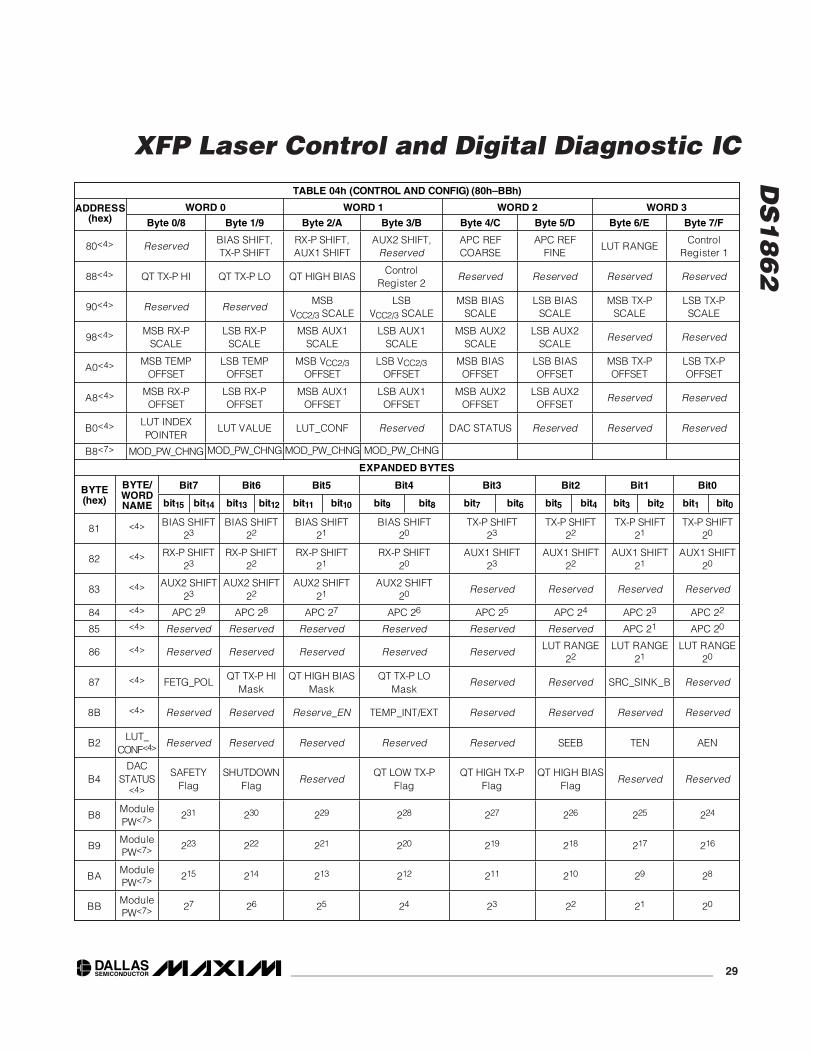
TABLE 04h (CONTROL AND CONFIG) (80h–BBh)
WORD 0 WORD 1 WORD 2 WORD 3 ADDRESS (hex) Byte 0/8 Byte 1/9 Byte 2/A Byte 3/B Byte 4/C Byte 5/D Byte 6/E Byte 7/F
80<4> ReservedBIAS SHIFT, TX-P SHIFT
RX-P SHIFT, AUX1 SHIFT
AUX2 SHIFT, Reserved
APC REF COARSE
APC REF FINE
LUT RANGE Control
Register 1
88<4> QT TX-P HI QT TX-P LO QT HIGH BIAS Control
Register 2 Reserved Reserved Reserved Reserved
90<4> Reserved ReservedMSB
VCC2/3 SCALE LSB
VCC2/3 SCALE MSB BIAS
SCALE LSB BIAS
SCALE MSB TX-P
SCALE LSB TX-P SCALE
98<4> MSB RX-P SCALE
LSB RX-P SCALE
MSB AUX1 SCALE
LSB AUX1 SCALE
MSB AUX2 SCALE
LSB AUX2 SCALE
Reserved Reserved
A0<4> MSB TEMP OFFSET
LSB TEMP OFFSET
MSB VCC2/3OFFSET
LSB VCC2/3OFFSET
MSB BIAS OFFSET
LSB BIAS OFFSET
MSB TX-P OFFSET
LSB TX-P OFFSET
A8<4> MSB RX-P OFFSET
LSB RX-P OFFSET
MSB AUX1 OFFSET
LSB AUX1 OFFSET
MSB AUX2 OFFSET
LSB AUX2 OFFSET
Reserved Reserved
B0<4> LUT INDEX POINTER
LUT VALUE LUT_CONF Reserved DAC STATUS Reserved Reserved Reserved
B8<7> MOD_PW_CHNG MOD_PW_CHNG MOD_PW_CHNG MOD_PW_CHNG
EXPANDED BYTES
Bit7 Bit6 Bit5 Bit4 Bit3 Bit2 Bit1 Bit0 BYTE (hex)
BYTE/ WORD NAME bit15 bit14 bit13 bit12 bit11 bit10 bit9 bit8 bit7 bit6 bit5 bit4 bit3 bit2 bit1 bit0
81 <4> BIAS SHIFT 23
BIAS SHIFT 22
BIAS SHIFT 21
BIAS SHIFT 20
TX-P SHIFT 23
TX-P SHIFT 22
TX-P SHIFT 21
TX-P SHIFT 20
82 <4> RX-P SHIFT 23
RX-P SHIFT 22
RX-P SHIFT 21
RX-P SHIFT 20
AUX1 SHIFT 23
AUX1 SHIFT 22
AUX1 SHIFT 21
AUX1 SHIFT 20
83 <4> AUX2 SHIFT 23
AUX2 SHIFT 22
AUX2 SHIFT 21
AUX2 SHIFT 20 Reserved Reserved Reserved Reserved
84 <4> APC 29 APC 28 APC 27 APC 26 APC 25 APC 24 APC 23 APC 22
85 <4> Reserved Reserved Reserved Reserved Reserved Reserved APC 21 APC 20
86 <4> Reserved Reserved Reserved Reserved ReservedLUT RANGE
22LUT RANGE
21LUT RANGE
20
87 <4> FETG_POL QT TX-P HI
Mask QT HIGH BIAS
Mask QT TX-P LO
Mask Reserved Reserved SRC_SINK_B Reserved
8B <4> Reserved Reserved Reserve_EN TEMP_INT/EXT Reserved Reserved Reserved Reserved
B2 LUT_
CONF<4> Reserved Reserved Reserved Reserved Reserved SEEB TEN AEN
B4 DAC
STATUS<4>
SAFETY Flag
SHUTDOWN Flag
ReservedQT LOW TX-P
Flag QT HIGH TX-P
Flag QT HIGH BIAS
Flag Reserved Reserved
B8 Module PW<7> 231 230 229 228 227 226 225 224
B9 Module PW<7> 223 222 221 220 219 218 217 216
BA Module PW<7> 215 214 213 212 211 210 29 28
BB Module PW<7> 27 26 25 24 23 22 21 20
DS
18
62
XFP Laser Control and Digital Diagnostic IC
30 ____________________________________________________________________
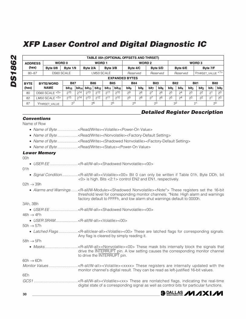
TABLE 05h (OPTIONAL OFFSETS AND THRSET)
WORD 0 WORD 1 WORD 2 WORD 3 ADDRESS (hex) Byte 0/8 Byte 1/9 Byte 2/A Byte 3/B Byte 4/C Byte 5/D Byte 6/E Byte 7/F
80–87 DS60 SCALE LM50 SCALE Reserved Reserved Reserved VTHRSET_VALUE <1>
EXPANDED BYTES
Bit7 Bit6 Bit5 Bit4 Bit3 Bit2 Bit1 Bit0 BYTE (hex)
BYTE/WORD NAME bit15 bit14 bit13 bit12 bit11 bit10 bit9 bit8 bit7 bit6 bit5 bit4 bit3 bit2 bit1 bit0
80 DS60 SCALE <5> 215 214 213 212 211 210 29 28 27 26 25 24 23 22 21 20
82 LM50 SCALE <5> 215 214 213 212 211 210 29 28 27 26 25 24 23 22 21 20
87 VTHRSET_VALUE 27 26 25 24 23 22 21 20
Detailed Register DescriptionConventionsName of Row
• Name of Byte ...................<Read/Write><Volatile><Power-On Value>
• Name of Byte ...................<Read/Write><Nonvolatile><Factory-Default Setting>
• Name of Byte ...................<Read/Write><Shadowed Nonvolatile><Factory-Default Setting>
• Name of Byte ...................<Read/Write><Status><Power-On Value>
Lower Memory00h
• USER EE ..........................<R-all/W-all><Shadowed Nonvolatile><00>01h
• Signal Condition...............<R-all/W-all><Volatile><00> Bit 0 can only be written if Table 01h, Byte DDh, bit<0> is high. Bits <2:1> control EN2 and EN1, respectively.
02h → 39h
• Alarms and Warnings ......<R-all/W-Module><Shadowed Nonvolatile><Note*> These registers set the 16-bitthreshold level for corresponding monitor channels. *Note: High alarm and warningsfactory default to FFFFh, and low alarm shut warnings default to 0000h.
3Ah, 3Bh
• USER EE ..........................<R-all/W-all><Shadowed Nonvolatile><00>46h → 4Fh
• USER SRAM.....................<R-all/W-all><Volatile><00>50h → 57h
• Latched Flags ..................<R-all/clear-all><Volatile><00> These are latched flags for corresponding signals.Any flag is cleared by simply reading it.
58h → 5Fh
• Masks...............................<R-all/W-all><Nonvolatile><00> These mask bits internally block the signals thatdrive the INTERRUPT pin. A low setting causes the corresponding monitor channelto drive the INTERRUPT pin.
60h → 6DhMonitor Values ...........................<R-all/W-all><Volatile><xxxx> These registers are internally updated with the
monitor channel’s digital result. They can be read as left-justified 16-bit values.6Eh
GCS1 .........................................<R-all/W-all><Volatile><xx> These are nonlatched flags, indicating the real-timedigital state of a corresponding signal as well as control bits for particular functions.

DS
18
62
XFP Laser Control and Digital Diagnostic IC
____________________________________________________________________ 31
Bit 0: DATA-NR. Bit is high until DS1862 has achieved power-up. Bit goes low, signaling that monitor channel datais ready to be read.
Bit 1: RX-LOS. Indicates optical loss of the signal and is updated within tLOS-ON.
Bit 2: INTERRUPT. Indicates the state of the INTERRUPT pin and is updated within tINIT_ON.
Bit 3: SOFT P-DOWN/RST. Read/Write bit that places the DS1862 in power-down mode. Toggle to reset. Maskedby Bit 5 of Byte DDh in Table 01h.
Bit 4: P-DOWN/RST. Indicates the digital state of the P-DOWN/RST pin and is updated within tPDR-ON.
Bit 5: MOD-NR State. Indicates the state of MOD-NR pin and is updated within tPDR-ON.
Bit 6: SOFT TX-D. Read/Write bit that disables (shuts down) IBIASSET and IMODSET. Masked by Bit 6 of Byte DDh in Table 01h.
Bit 7: TX-D. Indicates the digital state of the TX-D pin and is updated within tOFF.
6Fh• 6Fh GCS0 ........................<R-all/W-all><Status><xx> These are nonlatched flags, indicating the real-time
digital state of a corresponding signal.Bit 0: Reserved.
Bit 1: Reserved.
Bit 2: Reserved.
Bit 3: RX-CDR-NL not locked. Indicates LOL in Rx path CDR.
Bit 4: RX-NR State. Indicates a NOT READY condition in the Rx path.
Bit 5: Reserved.
Bit 6: TX-F State. Indicates a laser safety fault condition.
Bit 7: TX-NR State. Indicates a NOT READY condition on the Tx path.
74h
• POA..................................<R-all/W-all><Volatile><00> A high on bit 7 indicates that VCC3 is below the power-on analog trip point, POA.
76h
• PEC_EN..............................<R-all/W-all><Volatile><00> Bit 0 is used to enable PEC. A value of 1 enables PEC.77h → 7Ah
• Host PW Change .............<R-never/W-Host><Shadowed Nonvolatile P><00> This is the 32-bit location thatthe DS1862 uses to compare with the PWE to grant host password access. A Readresult is always <FFh>.
7Bh → 7Eh
• PWE.....................................<R-never/W-all><Volatile><00> This is the 32-bit location that is used to enter the hostand module password to gain access to the DS1862. A Read result is always <FFh>.
7Fh• Table Select .....................<R-all/W-all><Volatile><01> This is the 8-bit register that controls which section of
upper memory (table) is being addressed by I2C. A value of 00h and 01h results inaddressing Table 01h. Values above 05h are accepted, but do not correspond toany physical memory.
Table 01h80h → DBh
• USER EE ..........................<R-all/W-Module><Nonvolatile><00>DCh
• VCC2/3_SEL......................<R-all/W-Module><Shadowed Nonvolatile><00> Bit 0 of this register controlswhether VCC2 or VCC3 is internally measured by the VCC2/3 monitor channel. A ‘1’selects VCC2 to be measured.

DS
18
62
XFP Laser Control and Digital Diagnostic IC
32 ____________________________________________________________________
DDh
• LO MEM 6Eh EN ..............<R-all/W-Module><Shadowed Nonvolatile><00> If bit 5 is high, then bit 3 of 6Eh isnot masked. If bit 6 is high, then bit 6 of 6Eh is not masked. Bit 0 is the Lock_Bit. Ifset, Lower Memory address 01h, bit 0 is writable.
DEh
• AUX1/2 UNIT SEL ............<R-all/W-Module><Shadowed Nonvolatile><00> These two 4-bit values define whatis being measured on AUX1MON and AUX2MON. MSB is AUX1MON unit select andLSB is AUX2MON unit select. See Table 5 for more details.
DFh
• USER EE ..........................<R-all/W-Module><Shadowed Nonvolatile><00>
E0h → FFh
• USER EE ..........................<R-all/W-Module><Nonvolatile><00>
Table 02h80h → FFh
• USER EE ..........................<R-all/W-Host><Nonvolatile><00>
Table 03h80h → C7h
• LUT ..................................<R-Module/W-Module><Nonvolatile><00> These registers control the output cur-rent on MODSET as a function of temperature.
Table 04h80h → B8h
81h
• BIAS SHIFT ......................<R-Module/W-Module><Shadowed Nonvolatile><0> This 4-bit value in <7:4> defineshow many right-shifts IBIASMON monitor channel receives. The MSB is bit 7.
• TX-P SHIFT.......................<R-Module/W-Module><Shadowed Nonvolatile><0> This 4-bit value in <3:0> defineshow many right-shifts TX-P (BMD) monitor channel receives. The MSB is bit 3.
82h
• RX-P SHIFT ......................<R-Module/W-Module><Shadowed Nonvolatile><0> This 4-bit value in <7:4> defineshow many right-shifts RX-P (RSSI) monitor channel receives. The MSB is bit 7.
• AUX1 SHIFT .....................<R-Module/W-Module><Shadowed Nonvolatile><0> This 4-bit value in <3:0> defineshow many right-shifts AUX1MON monitor channel receives. The MSB is bit 3.
83h
• AUX2 SHIFT .....................<R-Module/W-Module><Shadowed Nonvolatile><0> This 4-bit value in <7:4> defineshow many right-shifts AUX2MON monitor channel receives. The MSB is bit 7.
84h
• APC REF COARSE...........<R-Module/W-Module><Shadowed Nonvolatile><00> This 8-bit value sets thecoarse APC current on BMD.

DS
18
62
XFP Laser Control and Digital Diagnostic IC
____________________________________________________________________ 33
85h
• APC REF FINE .................<R-Module/W-Module><Shadowed Nonvolatile><00> This 2-bit value in <1:0> setsthe fine APC current on BMD. The MSB is bit 1.
86h
• LUT RANGE .....................<R-Module/W-Module><Shadowed Nonvolatile><00> This 3-bit register in <2:0>sets the current range on MODSET. The MSB is bit 2.
87h
• Control Register 1 ............<R-Module/W-Module><Shadowed Nonvolatile><00>
Bit 0: Reserved.
Bit 1: SRC_SINK_B. If set, then BMD sources current; otherwise, BMD sinks current.
Bit 2: Reserved.
Bit 3: Reserved.
Bit 4: QT TX-P LO Mask. If set, then TX-P low does not have the ability to cause a safety fault.
Bit 5: QT HIGH BIAS Mask. If set, then HIGH BIAS does not have the ability to cause a safety fault.
Bit 6: QT TX-P HI Mask. If set, then TX-P high does not have the ability to cause a safety fault.
Bit 7: FETG_POL. If set, then FETG asserts with a high logic level; otherwise, it asserts with a low logic level.
88h
• QT TX-P HI .......................<R-Module/W-Module><Shadowed Nonvolatile><FF> This is the TX-P quick-tripthreshold setting that is used as a comparison to generate a TX-P high safety fault.
89h
• QT TX-P LO......................<R-Module/W-Module><Shadowed Nonvolatile><00> This is the TX-P quick-tripthreshold setting that is used as a comparison to generate a TX-P low safety fault.
8Ah
• QT HIGH BIAS .................<R-Module/W-Module><Shadowed Nonvolatile><FF> This is the TX-P quick-tripthreshold setting that is used as a comparison to generate a HIGH BIAS safety fault.
8Bh
• Control Register 2 ............<R-Module/W-Module><Shadowed Nonvolatile><00>
Bit 0: Reserved.
Bit 1: Reserved.
Bit 2: Reserved.
Bit 3: Reserved.
Bit 4: TEMP_INT/EXT. If set, then the LUT INDEX POINTER register is controlled by AUX2MON. Otherwise, theinternal temperature sensor controls the LUT.
Bit 5: Reserve_EN. If set, then VCC2/3 is actively updated in the monitor loop.
Bit 6: Reserved.
Bit 7: Reserved.

DS
18
62
XFP Laser Control and Digital Diagnostic IC
34 ____________________________________________________________________
92h
• VCC2/3 SCALE .................<R-Module/W-Module><Shadowed Nonvolatile><Factory Trimmed> This 16-bitregister controls the scale value for the VCC2/3 monitor channel.
94h
• BIAS SCALE.....................<R-Module/W-Module><Shadowed Nonvolatile><Factory Trimmed> This 16-bitregister controls the scale value for the BIAS monitor channel.
96h
• TX-P SCALE .....................<R-Module/W-Module><Shadowed Nonvolatile><Factory Trimmed> This 16-bitregister controls the scale value for the TX-P (BMD) monitor channel.
98h
• RX-P SCALE.....................<R-Module/W-Module><Shadowed Nonvolatile><Factory Trimmed> This 16-bitregister controls the scale value for the RX-P (RSSI) monitor channel.
9Ah
• AUX1 SCALE ...................<R-Module/W-Module><Shadowed Nonvolatile><Factory Trimmed> This 16-bitregister controls the scale value for the AUX1MON monitor channel.
9Ch
• AUX2 SCALE ...................<R-Module/W-Module><Shadowed Nonvolatile><Factory Trimmed> This 16-bitregister controls the scale value for the AUX2MON monitor channel.
A0h
• TEMP OFFSET .................<R-Module/W-Module><Shadowed Nonvolatile><Factory Trimmed> This 16-bitregister controls the offset value for the internal temperature monitor channel.
A2h
• VCC2/3 OFFSET................<R-Module/W-Module><Shadowed Nonvolatile><0000> This 16-bit register con-trols the offset value for the VCC2/3 monitor channel.
A4h
• BIAS OFFSET...................<R-Module/W-Module><Shadowed Nonvolatile><0000> This 16-bit register con-trols the offset value for the BIAS monitor channel.
A6h
• TX-P OFFSET ...................<R-Module/W-Module><Shadowed Nonvolatile><0000> This 16-bit register con-trols the offset value for the TX-P (BMD) monitor channel.
A8h
• RX-P OFFSET...................<R-Module/W-Module><Shadowed Nonvolatile><0000> This 16-bit register con-trols the offset value for the RX-P (RSSI) monitor channel.
AAh
• AUX1 OFFSET..................<R-Module/W-Module><Shadowed Nonvolatile><0000> This 16-bit register con-trols the offset value for the AUX1MON monitor channel.
ACh
• AUX2 OFFSET..................<R-Module/W-Module><Shadowed Nonvolatile><0000> This 16-bit register con-trols the offset value for the AUX2MON monitor channel.
B0h
• LUT INDEX POINTER.......<R-Module/W-Module><Volatile><xx> This register controls the index pointer valuefor the LUT. It is automatically updated (in normal operating mode) and can be reador overwritten using the TEN and AEN bits.
DS
18
62
XFP Laser Control and Digital Diagnostic IC
____________________________________________________________________ 35
B1h
• LUT VALUE ......................<R-Module/W-Module><Shadowed Nonvolatile><00> This register contains thefetched LUT value that drives the MODSET current. It can be read or overwritten todirectly control the MODSET current (manual mode).
B2h
• LUT_CONF.......................<R-Module/W-Module><Shadowed Nonvolatile><03>
Bit 0: AEN. A high on AEN enables data placed in the LUT VALUE register to drive MODSET.
Bit 1: TEN. A high on TEN enables the LUT INDEX POINTER to fetch data from the LUT.
Bit 2: SEEB. A high on SEEB disables EEPROM writes of Shadowed EEPROM locations.
Bit 3: Reserved.
Bit 4: Reserved.
Bit 5: Reserved.
Bit 6: Reserved.
Bit 7: Reserved.
B4h
• DAC STATUS ...................<R-Module/W-Module><Status><xx0xxx00b>
Bit 0: Reserved.
Bit 1: Reserved.
Bit 2: QT HIGH BIAS Flag. This flag indicates that the current entering BIASSET is above the threshold.
Bit 3: QT HIGH TX-P Flag. This flag indicates that TX-P is above the threshold.
Bit 4: QT LOW TX-P Flag. This flag indicates that TX-P is below the threshold.
Bit 5: Reserved.
Bit 6: SHUTDOWN Flag. A high indicates that the DS1862 is in shutdown mode and that FETG is asserted.
Bit 7: SAFETY Flag. A high indicates that a safety fault (quick trip) has occurred.
B8h
• MOD_PW_CHNG .............<R-never/W-Module><Shadowed Nonvolatile><00h> This is the 32-bit location thatthe DS1862 uses to compare with the PWE to grant module password access. ARead result is always <FFh>.
Table 05h80h
• DS60 SCALE....................<R-all/W-Factory><Nonvolatile><Factory Trimmed> This unique 16-bit value setsthe SCALE register for use with a DS60 temperature sensor on AUX2MON.
82h
• LM50 SCALE....................<R-all/W-Factory><Nonvolatile><Factory Trimmed> This unique 16-bit value setsthe SCALE register for use with a LM50 temperature sensor on AUX2MON.
87h
• VTHRSET_VALUE................<R-all/W-all><Shadowed Nonvolatile><80> This 8-bit value sets the voltage on thesignal conditioner voltage source, THRSET.
DS
18
62
XFP Laser Control and Digital Diagnostic IC
36 ____________________________________________________________________
Security/Password ProtectionThe DS1862 features two separate and independent32-bit passwords for important memory locations. Thehost password and the module password allow theirown allocated memory locations to be locked to pre-vent write and/or read access. To enhance the securityof the DS1862, the password entry and setting bytescan never be read.
To gain access to host-protected or module-protectedmemory locations, the correct 32-bit value must beentered into the password entry bytes (PWE) in either asingle 4-byte write, or 4 single-byte writes. To reprogrameither password, simply enter the appropriate currentpassword to gain memory access, write the new Host ormodule PW with one 4-byte write, and finally re-enter thenew password into the PWE to regain memory access.
Power-Up SequenceThe DS1862 does require a particular power-upsequence to ensure proper functionality. VCC3 shouldalways be applied first or at the same time as VCC2. Ifthis power-up sequence is not followed, then current canbe sourced out of VCC2 as if it was connected to VCC3with a resistor internal to the DS1862. If VCC2 is not usedthen it should be externally connected to VCC3.
Signal Conditioners—EN1 and EN2 and THRSET
Signal Conditioners—EN1 and EN2The EN1 and EN2 output pins are controlled by the bitsat address 01h, bits 2 and 1. The logic state of the pinsis directly analogous to the logical state of the register.EN1 and EN2 automatically change to a high and lowstate, respectively, during power-down mode asdescribed in the Power-Down Functionality section.
Signal Conditioners—THRSETA programmable voltage source, THRSET, is also pro-vided for use with signal conditioners. This source isprogrammable from 0 to 1V in 256 increments.
I2C and Packet ErrorChecking (PEC) Information
The DS1862 supports I2C data transfers as well as datatransfers with PEC. The slave address is unalterableand is set to A0h. The DS1862, however, does have anadditional dedicated pin, MOD-DESEL, which acts asan active-low chip select to enable communication. Seethe I2C Serial Interface and the I2C Operation UsingPacket Error Checking sections for details.
Precision SCALE RegisterSettings for AUX2MON
The DS1862 features a factory-trimmed SCALE valuefor use with DS60 or LM50 temperature sensors. Ifexternal temperature measurement on AUX2MON isused with one of these two sensors, the 16-bit SCALEvalue can be read from Table 05h and written into theSCALE register in Table 04h, Byte 9Ch and 9Dh. Thisoption allows for the most precise setting for SCALEwithout requiring additional trimming. Since the SCALEregister value is precisely trimmed at the factory, theOFFSET register will always be a nonunique value andcan simply be written into the OFFSET register. For theDS60, the value of EF0Ah in OFFSET completes theinternal calibration. For the LM50, the value of F380h inOFFSET completes the internal calibration.
I2C Serial InterfaceI2C Definitions
The following terminology is commonly used to describeI2C data transfers.
Master device: The master device controls the slavedevices on the bus. The master device generates SCLclock pulses and START and STOP conditions.
Slave devices: Slave devices send and receive data atthe master’s request.
Bus idle or not busy: Time between STOP and STARTconditions when both SDA and SCL are inactive and intheir logic-high states.
START condition: A START condition is generated bythe master to initiate a new data transfer with a slave.Transitioning SDA from high to low while SCL remainshigh generates a START condition. See Figure 14 forapplicable timing.
STOP condition: A STOP condition is generated by themaster to end a data transfer with a slave. TransitioningSDA from low to high while SCL remains high generatesa STOP condition. See Figure 14 for applicable timing.
REPEATED START condition: The master can use aREPEATED START condition at the end of one datatransfer to indicate that it will immediately initiate a newdata transfer following the current one. REPEATEDSTARTs are commonly used during read operations toidentify a specific memory address to begin a data trans-fer. A REPEATED START condition is issued identicallyto a normal START condition. See Figure 14 for applica-ble timing.

DS
18
62
XFP Laser Control and Digital Diagnostic IC
____________________________________________________________________ 37
Bit write: Transitions of SDA must occur during the lowstate of SCL. The data on SDA must remain valid andunchanged during the entire high pulse of SCL plus thesetup and hold time requirements (Figure 14). Data isshifted into the device during the rising edge of the SCL.
Bit read: At the end of a write operation, the mastermust release the SDA bus line for the proper amount ofsetup time (Figure 14) before the next rising edge ofSCL during a bit read. The device shifts out each bit ofdata on SDA at the falling edge of the previous SCLpulse and the data bit is valid at the rising edge of thecurrent SCL pulse. Remember that the master gener-ates all SCL clock pulses including when it is readingbits from the slave.
Acknowledgement (ACK and NACK): An Acknowl-edgement (ACK) or Not Acknowledge (NACK) is alwaysthe 9th bit transmitted during a byte transfer. The devicereceiving data (the master during a read or the slave dur-ing a write operation) performs an ACK by transmitting azero during the 9th bit. A device performs a NACK bytransmitting a one during the 9th bit. Timing (Figure 14)for the ACK and NACK is identical to all other bit writes.An ACK is the acknowledgment that the device is prop-erly receiving data. A NACK is used to terminate a readsequence or as an indication that the device is notreceiving data.
Byte write: A byte write consists of 8 bits of informationtransferred from the master to the slave (most signifi-cant bit first) plus a 1-bit acknowledgement from theslave to the master. The 8 bits transmitted by the mas-
ter are done according to the bit write definition and theacknowledgement is read using the bit read definition.
Byte read: A byte read is an 8-bit information transferfrom the slave to the master plus a 1-bit ACK or NACKfrom the master to the slave. The 8 bits of informationthat are transferred (most significant bit first) from theslave to the master are read by the master using the bitread definition, and the master transmits an ACK usingthe bit write definition to receive additional data bytes.The master must NACK the last byte read to terminatecommunication so the slave returns control of SDA tothe master.
Slave address byte: Each slave on the I2C busresponds to a slave addressing byte sent immediatelyfollowing a START condition. The slave address bytecontains the slave address in the most significant 7 bitsand the R/W bit in the least significant bit.
The DS1862’s slave address is 1010000Xb. The MOD-DESEL pin is used as a chip select, and allows thedevice to respond or ignore I2C communication thathas A0h as the device address. By writing the correctslave address with R/W = 0, the master indicates it willwrite data to the slave. If R/W = 1, the master will readdata from the slave. If an incorrect slave address iswritten, the DS1862 assumes the master is communi-cating with another I2C device and ignores the commu-nications until the next START condition is sent.
Memory address: During an I2C write operation, themaster must transmit a memory address to identify thememory location where the slave is to store the data.
SDA
SCL
tHD:STA
tLOW
tHIGH
tR tF
tBUF
tHD:DAT
tSU:DAT REPEATEDSTART
tSU:STA
tHD:STA
tSU:STO
tSP
STOP START
NOTE: TIMING IS REFERENCED TO VIL(MAX) AND VIH(MIN).
Figure 14. I2C Timing Diagram

DS
18
62
XFP Laser Control and Digital Diagnostic IC
38 ____________________________________________________________________
The memory address is always the second byte trans-mitted during a write operation following the slaveaddress byte.
I2C CommunicationWriting a single byte to a slave: The master mustgenerate a START condition, write the slave addressbyte (R/W = 0), write the memory address, write thebyte of data, and generate a STOP condition.Remember the master must read the slave’s acknowl-edgement during all byte write operations.
Writing multiple bytes to a slave: To write multiplebytes to a slave, the master generates a START condi-tion, writes the slave address byte (R/W = 0), writes thememory address, writes up to 4 data bytes, and gener-ates a STOP condition.
The DS1862 is capable of writing 1 to 4 bytes (referredto as one row or page) with a single write transaction.This is internally controlled by an address counter thatallows data to be written to consecutive addresses with-out transmitting a memory address before each databyte is sent. The address counter limits the write to onerow of the memory map. Attempts to write to additionalmemory rows without sending a STOP conditionbetween rows results in the address counter wrappingaround to the beginning address of the present row.
To prevent address wrapping from occurring, the mas-ter must send a STOP condition at the end of the row,and then wait for the bus free or EEPROM write time toelapse. Then the master can generate a new STARTcondition, and write the slave address byte (R/W = 0)and the first memory address of the next memory rowbefore continuing to write data.
Acknowledge polling: Any time EEPROM is written,the DS1862 requires the EEPROM write time (tW) afterthe STOP condition to write the contents of the row toEEPROM. During the EEPROM write time, the DS1862does not acknowledge its slave address because it isbusy. It is possible to take advantage of this phenome-non by repeatedly addressing the DS1862, whichallows the next row to be written as soon as the DS1862is ready to receive the data. The alternative to acknowl-edge polling is to wait for the maximum period of tW toelapse before attempting to write again to the DS1862.
EEPROM write cycles: When EEPROM writes occur,the DS1862 writes the whole EEPROM memory 4-byterow even if only a single byte on the row was modified.
Writes that do not modify all 4 bytes on the row areallowed and do not corrupt the remaining bytes ofmemory on the same row. Because the whole row iswritten, bytes on the row that were not modified duringthe transaction are still subject to a write cycle. Thiscan result in a whole row being worn out over time bywriting a single byte repeatedly. Writing a row one byteat a time wears out the EEPROM four times faster thanwriting the entire row at once. The DS1862’s EEPROMwrite cycles are specified in the Nonvolatile MemoryCharacteristics table.
Reading a single byte from a slave: Unlike the writeoperation that uses the memory address byte to definewhere the data is to be written, the read operationoccurs at the present value of the memory addresscounter. To read a single byte from the slave at thelocation currently in the address counter, the mastergenerates a START condition, writes the slave addressbyte with R/W = 1, reads the data byte with a NACK toindicate the end of the transfer, and generates a STOPcondition.
Manipulating the address counter for reads: Adummy write cycle can be used to force the addresscounter to a particular value. To do this the master gen-erates a START condition, writes the slave addressbyte (R/W = 0), writes the memory address where itdesires to read, generates a REPEATED START condi-tion, writes the slave address byte (R/W = 1), readsdata with ACK or NACK as applicable, and generates aSTOP condition.
See Figure 15 for a read example using the REPEATEDSTART condition to specify the starting memory location.
Reading multiple bytes from a slave: The read opera-tion can be used to read multiple bytes with a singletransfer. When reading bytes from the slave, the mastersimply ACKs the data byte if it desires to read anotherbyte before terminating the transaction. After the mas-ter reads the last byte it NACKs to indicate the end ofthe transfer and generates a STOP condition. This canbe done with or without modifying the addresscounter’s location before the read cycle. If the addresscounter reaches the last physical address, the internalindex pointer loops back to the first memory location ina given memory table. For example, if address FFh inTable 02h is read, the next byte of data to be returnedto the master is address 80h in Table 02h, not 00h inlower memory.

DS
18
62
XFP Laser Control and Digital Diagnostic IC
____________________________________________________________________ 39
I2C Operation UsingPacket Error Checking
Read Operation withPacket Error Checking
Packet error checking during reads is supported by theDS1862. Information is transferred form the DS1862 inmuch the same way as conventional I2C protocol, how-ever, an extra CRC field is added and checked. Themaster still begins by sending the device address (A0hfor DS1862), then the index pointer to the memoryaddress of interest. The next byte transferred, however,is the value of the intended number of bytes to be read.The calculation of the CRC-8 includes and requires theexplicit starting memory address to be included as thesecond transferred byte (dummy write byte). Next, theslave transfers the data back as the master acknowl-edges. Only 1 to 128 bytes can be sequentially readduring one transmission while using PEC. After themaster reads the intended number of bytes, the CRC-8value is transmitted by the DS1862. The master ends
the communication with a NACK and a STOP. SeeFigure 16 for a graphical representation. The CRC-8 iscalculated starting with the MSB of the memoryaddress pointer, number of bytes to read, and the readdata. The master can then verify the CRC-8 value andreject the read data if the CRC-8 value does not corre-spond to the received CRC value. The CRC-8 must becalculated by using the following polynomial for bothreads and writes:
C(x) = X8 +X2 + X + 1
Write Operation withPacket Error Checking
Packet error checking during writes is also supportedby the DS1862. Information is written to the DS1862 inmuch the same way as conventional I2C protocol, how-ever, an extra CRC field is added and checked. Themaster still begins by sending the device address, thenthe index pointer to the memory address of interest.The next byte, however, is the value of the intendednumber of bytes to be written. The calculation of the
X X X X X X X X
1 0 1 0 0 000
1 0 1 0 0 000
1 0 1 0 0 000 1 0 1 0 0 000
1 0 1 0 0 0001 0 1 0 0 000
COMMUNICATIONS KEY
WRITE A SINGLE BYTE
WRITE UP TO A 4-BYTE PAGE WITH A SINGLE TRANSACTION
READ A SINGLE BYTE WITH A DUMMY WRITE CYCLE TO SET THE ADDRESS COUNTER
READ MULTIPLE BYTES WITH A DUMMY WRITE CYCLE TO SET THE ADDRESS COUNTER
8-BIT ADDRESS OR DATA
WHITE BOXES INDICATE THE MASTER IS CONTROLLING SDA
THE FIRST BYTE SENT AFTER A START CONDITION ISALWAYS THE SLAVE ADDRESS FOLLOWED BY THEREAD/WRITE BIT.
SHADED BOXES INDICATE THE SLAVE IS CONTROLLING SDA
START ACK
NOTACK
S
S
S
S
S
A
A
A
A
A
A
A P
A
A SR
SRA
A
A P
N P
N P
A A
DATA
DATA
DATA
DATA
DATA
DATADATA
MEMORY ADDRESS
MEMORY ADDRESS
MEMORY ADDRESS
MEMORY ADDRESS
DATAA A
A
P N
SR
STOP
REPEATEDSTART
NOTE:ALL BYTES ARE SENT MOST SIGNIFICANT BIT FIRST.
Figure 15. I2C Communications Examples

DS
18
62
XFP Laser Control and Digital Diagnostic IC
40 ____________________________________________________________________
CRC-8 includes and requires the explicit starting mem-ory address to be included as the second transferredbyte. Next, the master transfers the data as the DS1862acknowledges. Only 4 bytes can be sequentially writtenduring one transmission while using PEC. After themaster writes the intended number of bytes, the CRC-8value should be transmitted. Following the CRC-8 byte,the master should transmit the CAB byte (CRC Add-onByte). At this point, the DS1862 sends an ACK if theCRC-8 matches its internal calculated value or a NACKif not. Finally, the master should end the communicationand send a STOP. See Figure 16 for a graphical repre-sentation. The CRC-8 is calculated starting with theMSB of the memory address pointer, number of bytesto be written, and the written data. The master can thenpoll the last ACK or NACK for successful transfer ofwritten data.
For more information on I2C PEC communications, referto the XFP and/or SMBus 2.0 standard.
Applications InformationCalibrating APC and Extinction Ratio
Before calibrating, the APC register should be set to alow value to ensure the laser’s maximum power level isnot exceeded before the power level is calibrated.Additionally, the ER should be set to a minimum valueto ensure that a data test pattern does not cause thelaser to shut off. Once the APC and ER registers are atminimal values, enable a data pattern and calibrate theaverage power level.
Calibrating the Average Power LevelWhile sending data through the laser diode, increasethe value in the APC register until the light outputmatches the desired average power level. The averagepower level is the arithmetic average of the ‘1’ and ‘0’power levels.
X X X X X X X X
1 0 1 0 0 000
1 0 1 0 0 000 1 0 1 0 0 000
COMMUNICATIONS KEY
WRITE UP TO A 4-BYTE PAGE WITH A SINGLE TRANSACTION USING PEC
READ 1–128 BYTES WITH A DUMMY WRITE CYCLE TO SET THE ADDRESS COUNTER
8-BIT ADDRESS OR DATA
WHITE BOXES INDICATE THE MASTER IS CONTROLLING SDA
THE FIRST BYTE SENT AFTER A START CONDITION ISALWAYS THE SLAVE ADDRESS FOLLOWED BY THEREAD/WRITE BIT.
SHADED BOXES INDICATE THE SLAVE IS CONTROLLING SDA
START ACK
NOTACK
S
S
S
A
A
A
A
A
A
A
SRA
A
N P
A A
CRC-8 VALUEDATADATA
DATA
CRC-8 VALUEDATA
DATA
MEMORY ADDRESS ANUMBER OF BYTES
NUMBER OF BYTESMEMORY ADDRESS
DATAA A
A
P N
SR
STOP
REPEATEDSTART
NOTE:ALL BYTES ARE SENT MOST SIGNIFICANT BIT FIRST.
A (IF CRC-8 IS CORRECT) PDATA
Figure 16. I2C PEC Communications Examples

DS
18
62
XFP Laser Control and Digital Diagnostic IC
____________________________________________________________________ 41
Power-Supply DecouplingTo achieve best results, it is recommended that thepower supply is decoupled with a 0.01μF or a 0.1μFcapacitor. Use high-quality, ceramic, surface-mountcapacitors, and mount the capacitors as close as pos-sible to the VCC2/VCC3 and GND pins to minimize leadinductance.
SDA and SCL Pullup ResistorsSDA is an open-collector bidirectional data pin on theDS1862 that requires a pullup resistor to realize highlogic levels. Either an open-collector output with a pullupresistor or a push-pull output driver can be utilized forthe SCL input. Pullup resistor values should be chosento ensure that the rise and fall times listed in the I2C ACElectrical Characteristics are within specification.
*ADDITIONAL MONITORS NOT USED IN THIS EXAMPLE.
SDA
SCL
4.7kΩ
RX-LOS
MOD-NR
VCC2
TX-D
INTERRUPT
MOD-DESEL
VCC3
EN1
SC-TX-LOS
GND
EN2
BMD
BIASSET
MODSET
FETG
IBIASMON
RSSI
SC-RX-LOL
SC-RX-LOS
THRSET
AUX1MON
AUX2MON
P-DOWN/RST
HOST
1.8V 3.3V
3.3V
0.1μF0.1μF
BIASSET
MODSET
MONITOR
LASERDRIVER
10nF
OUT
LIMITINGAMP
LOS
LOL
FCTL2
FCTL1
VTH
LOSFCTL2
FCTL1
EQUALIZER
RECEIVER CURRENT SENSE (VOLTAGE)
TX-DISABLETX-DISABLE DISABLE
1nF
*
1kΩ
DS1862
MAX3975
MAX3991
MAX3992
4.7kΩ
3.3V
10kΩ
3.3V
10kΩ
3.3V
10kΩ
3.3V
Typical Operating Circuit

DS
18
62
XFP Laser Control and Digital Diagnostic IC
42 ____________________________________________________________________
Chip InformationTRANSISTOR COUNT: 75,457
SUBSTRATE CONNECTED TO GROUND
Package InformationFor the latest package outline information and land patterns, goto www.maxim-ic.com/packages.
PACKAGE TYPE PACKAGE CODE DOCUMENT NO.
25 CSBGA X25-1 21-0361

DS
18
62
XFP Laser Control and Digital Diagnostic IC
Maxim cannot assume responsibility for use of any circuitry other than circuitry entirely embodied in a Maxim product. No circuit patent licenses areimplied. Maxim reserves the right to change the circuitry and specifications without notice at any time.
Maxim Integrated Products, 120 San Gabriel Drive, Sunnyvale, CA 94086 408-737-7600 ____________________ 43
© 2007 Maxim Integrated Products Maxim is a registered trademark of Maxim Integrated Products, Inc.
is a registered trademark of Dallas Semiconductor Corporation.
Revision HistoryREVISION NUMBER
REVISION DATE
DESCRIPTIONPAGES
CHANGED
0 2/06 Initial release. —
1 12/07
Removed I2C disclaimer.
Corrected password level control for B8h of Table 04h from <4> to <7>.
Corrected grammar for Byte 01h SRAM description: “bits” after “Byte DDh” changed to “bit”.
Clarified the function of the DDh enable bits, added the following sentence to the 6Eh Bit 3 description: “Masked by Bit 5 of Byte DDh in Table 01h.”
Clarified the function of the DDh enable bits, added the following sentence to the 6Eh Bit 6 description: “Masked by Bit 6 of Byte DDh in Table 01h.”
Clarified the Read function of the Host PW Change and PWE descriptions, added the following sentence to both descriptions: “A Read result is always <FFh>.”
Corrected and clarified the Module password value, changed the current description to: <R-never / W-Module><Shadowed Nonvolatile><00h> This is the 32-bit location that the DS1862 uses to compare with the PWE to grant Module password access. A Read result is always <FFh>.
Added Package Information table.
1, 29–31, 35, 42