xilinx ds302 virtex-4 fpga data sheet: dc and switching ... · pdf filevirtex-4 fpga data...
TRANSCRIPT

DS302 (v3.7) September 9, 2009 www.xilinx.comProduct Specification 1
© 2004–2009 Xilinx, Inc. XILINX, the Xilinx logo, Virtex, Spartan, ISE, and other designated brands included herein are trademarks of Xilinx in the United States and other countries. The PowerPC name and logo are registered trademarks of IBM Corp. and used under license. PCI, PCI Express, PCIe, and PCI-X are trademarks of PCI-SIG. All other trademarks are the property of their respective owners.
Virtex-4 FPGA Electrical CharacteristicsVirtex®-4 FPGAs are available in -12, -11, and -10 speedgrades, with -12 having the highest performance.
Virtex-4 FPGA DC and AC characteristics are specified forboth commercial and industrial grades. Except the operat-ing temperature range or unless otherwise noted, all the DCand AC electrical parameters are the same for a particularspeed grade (that is, the timing characteristics of a -10speed grade industrial device are the same as for a -10speed grade commercial device). However, only selectedspeed grades and/or devices might be available in theindustrial range.
All supply voltage and junction temperature specificationsare representative of worst-case conditions. The parame-ters included are common to popular designs and typicalapplications.
This Virtex-4 FPGA Data Sheet is part of an overall set ofdocumentation on the Virtex-4 family of FPGAs that is avail-able on the Xilinx website:
• Virtex-4 Family Overview, DS112• Virtex-4 FPGA User Guide, UG070• Virtex-4 FPGA Configuration Guide, UG071• XtremeDSP for Virtex-4 FPGAs User Guide, UG073• Virtex-4 FPGA Packaging and Pinout Specification,
UG075• Virtex-4 FPGA PCB Designer’s Guide, UG072• Virtex-4 RocketIO™ Multi-Gigabit Transceiver User
Guide, UG076• Virtex-4 FPGA Embedded Tri-Mode Ethernet MAC
User Guide, UG074• PowerPC® 405 Processor Block Reference Guide,
UG018
All specifications are subject to change without notice.
Virtex-4 FPGA DC Characteristics
0
Virtex-4 FPGA Data Sheet: DC and Switching Characteristics
DS302 (v3.7) September 9, 2009 0 0 Product Specification
Table 1: Absolute Maximum Ratings
Symbol Description Units
VCCINT Internal supply voltage relative to GND –0.5 to 1.32 V
VCCAUX Auxiliary supply voltage relative to GND –0.5 to 3.0 V
VCCO Output drivers supply voltage relative to GND –0.5 to 3.75 V
VBATT Key memory battery backup supply –0.5 to 4.05 V
VREF Input reference voltage –0.3 to 3.75 V
VIN
I/O input voltage relative to GND (all user and dedicated I/Os)
–0.75 to 4.05 V
I/O input voltage relative to GND (restricted to maximum of 100 user I/Os)(3,4)
–0.95 to 4.4(Commercial Temperature)
–0.85 to 4.3(Industrial Temperature)
V
2.5V or below I/O input voltage relative to GND (user and dedicated I/Os)
–0.75 to VCCO +0.5 V
IINCurrent applied to an I/O pin, powered or unpowered ±100 mA
Total current applied to all I/O pins, powered or unpowered ±200 mA

Virtex-4 FPGA Data Sheet: DC and Switching Characteristics
DS302 (v3.7) September 9, 2009 www.xilinx.comProduct Specification 2
VTS
Voltage applied to 3-state 3.3V output(all user and dedicated I/Os)
–0.75 to 4.05 V
Voltage applied to 3-state 3.3V output(restricted to maximum of 100 user I/Os)(3,4)
–0.95 to 4.4(Commercial Temperature)
–0.85 to 4.3(Industrial Temperature)
V
2.5V or below I/O input voltage relative to GND (user and dedicated I/Os)
–0.75 to VCCO +0.5 V
AVCCAUXRXReceive auxiliary supply voltage relative to analog ground, GNDA(RocketIO pins)
–0.5 to 1.32 V
AVCCAUXTXTransmit auxiliary supply voltage relative to analog ground, GNDA(RocketIO pins)
–0.5 to 1.32 V
AVCCAUXMGTManagement auxiliary supply voltage relative to analog ground, GNDA(RocketIO pins)
–0.5 to 3.0 V
VTRX Terminal receive supply voltage relative to GND –0.5 to 3.0 V
VTTX Terminal transmit supply voltage relative to GND –0.5 to 1.65 V
TSTG Storage temperature (ambient) –65 to 150 ° C
TSOL Maximum soldering temperature(2) +220 ° C
TJ Maximum junction temperature(2) +125 ° C
Notes: 1. Stresses beyond those listed under Absolute Maximum Ratings might cause permanent damage to the device. These are stress ratings only, and
functional operation of the device at these or any other conditions beyond those listed under Operating Conditions is not implied. Exposure to Absolute Maximum Ratings conditions for extended periods of time might affect device reliability.
2. For soldering guidelines and thermal considerations, see the Virtex-4 Packaging and Pinout Specification on the Xilinx website.3. When using more than 100 3.3V I/Os, refer to the Virtex-4 FPGA User Guide, Chapter 6, “3.3V I/O Design Guidelines.” 4. For more flexibility in specific designs, a maximum of 100 user I/Os can be stressed beyond the normal spec for no more than 20% of a data period.
There are no bank restrictions.
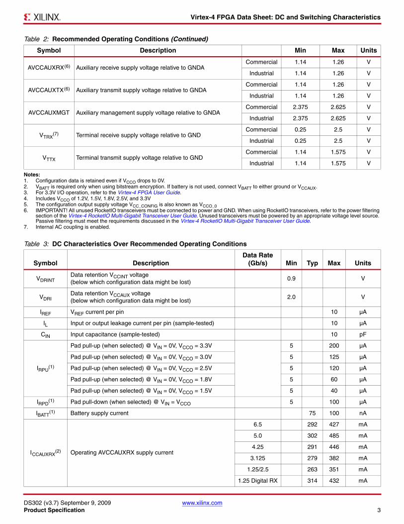
Table 2: Recommended Operating Conditions
Symbol Description Min Max Units
VCCINT
Internal supply voltage relative to GND, TJ = 0° C to +85° C Commercial 1.14 1.26 V
Internal supply voltage relative to GND, TJ = –40° C to +100° C Industrial 1.14 1.26 V
VCCAUX
Auxiliary supply voltage relative to GND, TJ = 0° C to +85° C Commercial 2.375 2.625 V
Auxiliary supply voltage relative to GND, TJ = –40° C to +100° C Industrial 2.375 2.625 V
VCCO(1,3,4,5)
Supply voltage relative to GND, TJ = 0° C to +85° C Commercial 1.14 3.45 V
Supply voltage relative to GND, TJ = –40° C to +100° C Industrial 1.14 3.45 V
VIN
3.3V supply voltage relative to GND, TJ = 0° C to +85° C Commercial GND – 0.20 3.45 V
3.3V supply voltage relative to GND, TJ = –40° C to +100° C Industrial GND – 0.20 3.45 V
2.5V and below supply voltage relative to GND, TJ = 0° C to +85° C
Commercial GND – 0.20 VCCO + 0.2 V
2.5V and below supply voltage relative to GND, TJ = –40° C to +100° C
Industrial GND – 0.20 VCCO + 0.2 V
IINMaximum current through any pin in a powered or unpowered bank when forward biasing the clamp diode.
Commercial 10 mA
Industrial 10 mA
VBATT(2)
Battery voltage relative to GND, TJ = 0° C to +85° C Commercial 1.0 3.6 V
Battery voltage relative to GND, TJ = –40° C to +100° C Industrial 1.0 3.6 V
Table 1: Absolute Maximum Ratings (Continued)
Symbol Description Units
Virtex-4 FPGA Data Sheet: DC and Switching Characteristics
DS302 (v3.7) September 9, 2009 www.xilinx.comProduct Specification 3
AVCCAUXRX(6) Auxiliary receive supply voltage relative to GNDACommercial 1.14 1.26 V
Industrial 1.14 1.26 V
AVCCAUXTX(6) Auxiliary transmit supply voltage relative to GNDACommercial 1.14 1.26 V
Industrial 1.14 1.26 V
AVCCAUXMGT Auxiliary management supply voltage relative to GNDACommercial 2.375 2.625 V
Industrial 2.375 2.625 V
VTRX(7) Terminal receive supply voltage relative to GND
Commercial 0.25 2.5 V
Industrial 0.25 2.5 V
VTTX Terminal transmit supply voltage relative to GNDCommercial 1.14 1.575 V
Industrial 1.14 1.575 V
Notes: 1. Configuration data is retained even if VCCO drops to 0V.2. VBATT is required only when using bitstream encryption. If battery is not used, connect VBATT to either ground or VCCAUX.3. For 3.3V I/O operation, refer to the Virtex-4 FPGA User Guide.4. Includes VCCO of 1.2V, 1.5V, 1.8V, 2.5V, and 3.3V5. The configuration output supply voltage VCC_CONFIG is also known as VCCO_06. IMPORTANT! All unused RocketIO transceivers must be connected to power and GND. When using RocketIO transceivers, refer to the power filtering
section of the Virtex-4 RocketIO Multi-Gigabit Transceiver User Guide. Unused transceivers must be powered by an appropriate voltage level source. Passive filtering must meet the requirements discussed in the Virtex-4 RocketIO Multi-Gigabit Transceiver User Guide.
7. Internal AC coupling is enabled.
Table 2: Recommended Operating Conditions (Continued)
Symbol Description Min Max Units
Table 3: DC Characteristics Over Recommended Operating Conditions
Symbol DescriptionData Rate
(Gb/s) Min Typ Max Units
VDRINTData retention VCCINT voltage(below which configuration data might be lost)
0.9 V
VDRIData retention VCCAUX voltage (below which configuration data might be lost)
2.0 V
IREF VREF current per pin 10 µA
IL Input or output leakage current per pin (sample-tested) 10 µA
CIN Input capacitance (sample-tested) 10 pF
IRPU(1)
Pad pull-up (when selected) @ VIN = 0V, VCCO = 3.3V 5 200 µA
Pad pull-up (when selected) @ VIN = 0V, VCCO = 3.0V 5 125 µA
Pad pull-up (when selected) @ VIN = 0V, VCCO = 2.5V 5 120 µA
Pad pull-up (when selected) @ VIN = 0V, VCCO = 1.8V 5 60 µA
Pad pull-up (when selected) @ VIN = 0V, VCCO = 1.5V 5 40 µA
IRPD(1) Pad pull-down (when selected) @ VIN = VCCO 5 100 µA
IBATT(1) Battery supply current 75 100 nA
ICCAUXRX(2) Operating AVCCAUXRX supply current
6.5 292 427 mA
5.0 302 485 mA
4.25 291 446 mA
3.125 279 382 mA
1.25/2.5 263 351 mA
1.25 Digital RX 314 432 mA

Virtex-4 FPGA Data Sheet: DC and Switching Characteristics
DS302 (v3.7) September 9, 2009 www.xilinx.comProduct Specification 4
ICCAUXTX(2) Operating AVCCAUXTX supply current
6.5 170 339 mA
5.0 180 355 mA
4.25 173 330 mA
3.125 165 307 mA
2.5 157 298 mA
1.25 151 295 mA
ICCAUXMGT(2) Operating AVCCAUXMGT supply current 3 5 mA
ITTX(2) Operating ITTX supply current when transmitter is AC coupled
or VTTX = VTRX100 210 mA
ITRX(2,3) Operating ITRX supply current when receiver is AC coupled or
VTTX = VTRX12 24 mA
n Temperature diode ideality factor 1.02 n
PCPU Power dissipation of PowerPC 405 processor block 0.45 mW/MHz
r Series resistance 2 Ω
Notes: 1. Values are specified at nominal voltage, 25°C.2. Typical ICC numbers given per tile with both MGTs operating with default settings. Maximum ICC numbers given per tile with both MGTs operating with
maximum amplitude and emphasis settings.3. Varies with AC / DC coupling.
Table 3: DC Characteristics Over Recommended Operating Conditions (Continued)
Symbol DescriptionData Rate
(Gb/s) Min Typ Max Units
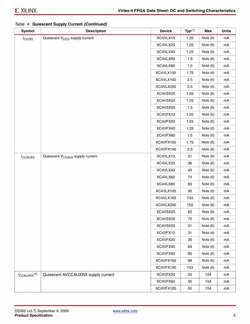
Table 4: Quiescent Supply Current
Symbol Description Device Typ(1) Max Units
ICCINTQ Quiescent VCCINT supply current XC4VLX15 46 Note (6) mA
XC4VLX25 77 Note (6) mA
XC4VLX40 121 Note (6) mA
XC4VLX60 167 Note (6) mA
XC4VLX80 220 Note (6) mA
XC4VLX100 292 Note (6) mA
XC4VLX160 384 Note (6) mA
XC4VLX200 489 Note (6) mA
XC4VSX25 94 Note (6) mA
XC4VSX35 140 Note (6) mA
XC4VSX55 271 Note (6) mA
XC4VFX12 47 Note (6) mA
XC4VFX20 71 Note (6) mA
XC4VFX40 139 Note (6) mA
XC4VFX60 203 Note (6) mA
XC4VFX100 311 Note (6) mA
XC4VFX140 442 Note (6) mA
Virtex-4 FPGA Data Sheet: DC and Switching Characteristics
DS302 (v3.7) September 9, 2009 www.xilinx.comProduct Specification 5
ICCOQ Quiescent VCCO supply current XC4VLX15 1.25 Note (6) mA
XC4VLX25 1.25 Note (6) mA
XC4VLX40 1.25 Note (6) mA
XC4VLX60 1.5 Note (6) mA
XC4VLX80 1.5 Note (6) mA
XC4VLX100 1.75 Note (6) mA
XC4VLX160 2.5 Note (6) mA
XC4VLX200 2.5 Note (6) mA
XC4VSX25 1.25 Note (6) mA
XC4VSX35 1.25 Note (6) mA
XC4VSX55 1.5 Note (6) mA
XC4VFX12 1.25 Note (6) mA
XC4VFX20 1.25 Note (6) mA
XC4VFX40 1.25 Note (6) mA
XC4VFX60 1.5 Note (6) mA
XC4VFX100 1.75 Note (6) mA
XC4VFX140 2.5 Note (6) mA
ICCAUXQ Quiescent VCCAUX supply current XC4VLX15 31 Note (6) mA
XC4VLX25 36 Note (6) mA
XC4VLX40 43 Note (6) mA
XC4VLX60 74 Note (6) mA
XC4VLX80 83 Note (6) mA
XC4VLX100 95 Note (6) mA
XC4VLX160 133 Note (6) mA
XC4VLX200 150 Note (6) mA
XC4VSX25 62 Note (6) mA
XC4VSX35 70 Note (6) mA
XC4VSX55 91 Note (6) mA
XC4VFX12 31 Note (6) mA
XC4VFX20 35 Note (6) mA
XC4VFX40 69 Note (6) mA
XC4VFX60 80 Note (6) mA
XC4VFX100 98 Note (6) mA
XC4VFX140 143 Note (6) mA
ICCAUXRX(4) Quiescent AVCCAUXRX supply current XC4VFX20 25 154 mA
XC4VFX60 35 154 mA
XC4VFX100 50 154 mA
Table 4: Quiescent Supply Current (Continued)
Symbol Description Device Typ(1) Max Units

Virtex-4 FPGA Data Sheet: DC and Switching Characteristics
DS302 (v3.7) September 9, 2009 www.xilinx.comProduct Specification 6
ICCAUXTX(4) Quiescent AVCCAUXTX supply current XC4VFX20 10 44 mA
XC4VFX60 15 44 mA
XC4VFX100 20 44 mA
ITTX(4,5) Quiescent VTTX supply current XC4VFX20 1 2 mA
XC4VFX60 1 2 mA
XC4VFX100 1 2 mA
ITRX(4,5) Quiescent VTRX supply current XC4VFX20 1 2 mA
XC4VFX60 1 2 mA
XC4VFX100 1 2 mA
IAUXMGT(4) Quiescent VAUXMGT supply current XC4VFX20 1 2 mA
XC4VFX60 1 2 mA
XC4VFX100 1 2 mA
Notes: 1. Typical values are specified at nominal voltage, 25°C.2. Typical values are for blank configured devices with no output current loads, no active input pull-up resistors, all I/O pins are 3-state and floating.3. If DCI or differential signaling is used, more accurate quiescent current estimates can be obtained by using the Power Estimator or XPower tool.4. Given for entire die. Powered and unconfigured.5. Unconnected (if channel is driven to voltage).6. Use the XPower Estimator (XPE) tool to calculate maximum static power for specific process, voltage, and temperature conditions.
Table 4: Quiescent Supply Current (Continued)
Symbol Description Device Typ(1) Max Units
Virtex-4 FPGA Data Sheet: DC and Switching Characteristics
DS302 (v3.7) September 9, 2009 www.xilinx.comProduct Specification 7
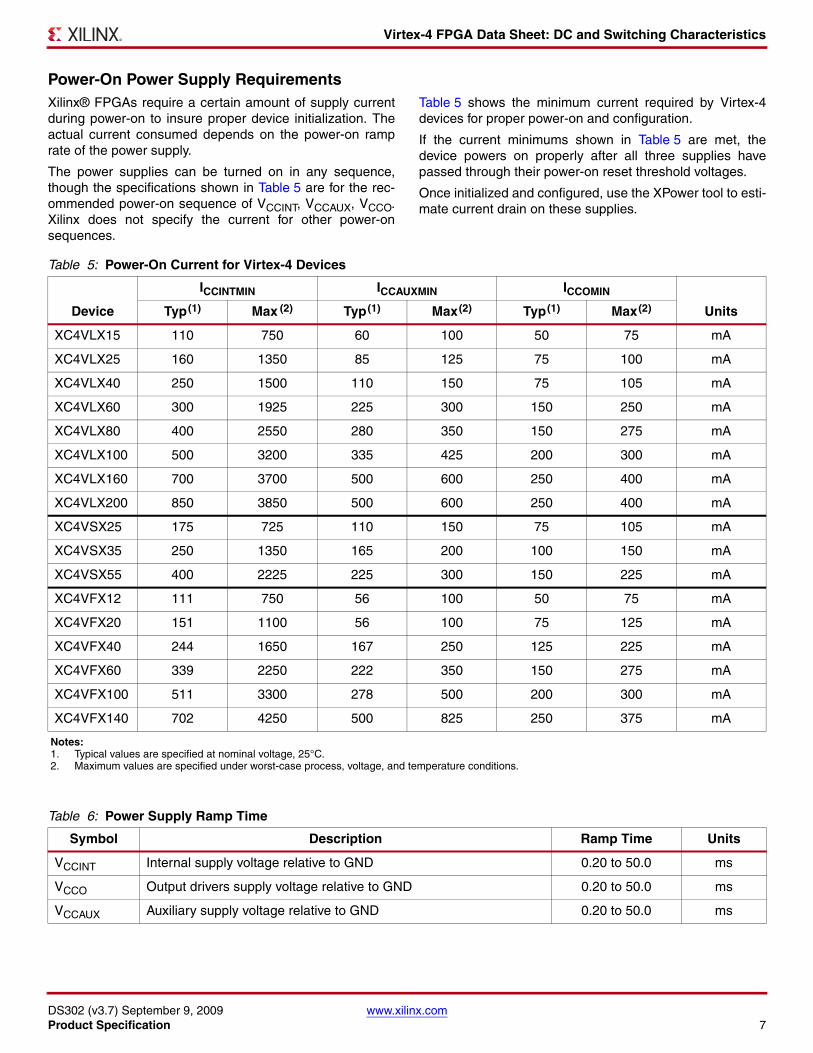
Power-On Power Supply RequirementsXilinx® FPGAs require a certain amount of supply currentduring power-on to insure proper device initialization. Theactual current consumed depends on the power-on ramprate of the power supply.
The power supplies can be turned on in any sequence,though the specifications shown in Table 5 are for the rec-ommended power-on sequence of VCCINT, VCCAUX, VCCO.Xilinx does not specify the current for other power-onsequences.
Table 5 shows the minimum current required by Virtex-4devices for proper power-on and configuration.
If the current minimums shown in Table 5 are met, thedevice powers on properly after all three supplies havepassed through their power-on reset threshold voltages.
Once initialized and configured, use the XPower tool to esti-mate current drain on these supplies.
Table 5: Power-On Current for Virtex-4 Devices
Device
ICCINTMIN ICCAUXMIN ICCOMIN
UnitsTyp(1) Max (2) Typ(1) Max(2) Typ(1) Max(2)
XC4VLX15 110 750 60 100 50 75 mA
XC4VLX25 160 1350 85 125 75 100 mA
XC4VLX40 250 1500 110 150 75 105 mA
XC4VLX60 300 1925 225 300 150 250 mA
XC4VLX80 400 2550 280 350 150 275 mA
XC4VLX100 500 3200 335 425 200 300 mA
XC4VLX160 700 3700 500 600 250 400 mA
XC4VLX200 850 3850 500 600 250 400 mA
XC4VSX25 175 725 110 150 75 105 mA
XC4VSX35 250 1350 165 200 100 150 mA
XC4VSX55 400 2225 225 300 150 225 mA
XC4VFX12 111 750 56 100 50 75 mA
XC4VFX20 151 1100 56 100 75 125 mA
XC4VFX40 244 1650 167 250 125 225 mA
XC4VFX60 339 2250 222 350 150 275 mA
XC4VFX100 511 3300 278 500 200 300 mA
XC4VFX140 702 4250 500 825 250 375 mA
Notes: 1. Typical values are specified at nominal voltage, 25°C.2. Maximum values are specified under worst-case process, voltage, and temperature conditions.
Table 6: Power Supply Ramp Time
Symbol Description Ramp Time Units
VCCINT Internal supply voltage relative to GND 0.20 to 50.0 ms
VCCO Output drivers supply voltage relative to GND 0.20 to 50.0 ms
VCCAUX Auxiliary supply voltage relative to GND 0.20 to 50.0 ms

Virtex-4 FPGA Data Sheet: DC and Switching Characteristics
DS302 (v3.7) September 9, 2009 www.xilinx.comProduct Specification 8
SelectIO™ DC Input and Output LevelsValues for VIL and VIH are recommended input voltages.Values for IOL and IOH are guaranteed over the recom-mended operating conditions at the VOL and VOH testpoints. Only selected standards are tested. These are cho-sen to ensure that all standards meet their specifications.
The selected standards are tested at a minimum VCCO withthe respective VOL and VOH voltage levels shown. Otherstandards are sample tested.
Table 7: SelectIO DC Input and Output Levels
IOSTANDARDAttribute
VIL VIH VOL VOH IOL IOH
V, Min V, Max V, Min V, Max V, Max V, Min mA mA
LVTTL –0.2 0.8 2.0 3.45 0.4 2.4 Note(3) Note(3)
LVCMOS33,LVDCI33
–0.2 0.8 2.0 3.45 0.4 VCCO – 0.4 Note(3) Note(3)
LVCMOS25,LVDCI25
–0.3 0.7 1.7 VCCO + 0.3 0.4 VCCO – 0.4 Note(3) Note(3)
LVCMOS18,LVDCI18
–0.3 35% VCCO 65% VCCO VCCO + 0.3 0.4 VCCO – 0.45 Note(4) Note(4)
LVCMOS15,LVDCI15
–0.3 35% VCCO 65% VCCO VCCO + 0.3 0.4 VCCO – 0.45 Note(4) Note(4)
PCI33_3(5) –0.2 30% VCCO 50% VCCO VCCO 10% VCCO 90% VCCO 1.5 –0.5
PCI66_3(5) –0.2 30% VCCO 50% VCCO VCCO 10% VCCO 90% VCCO 1.5 –0.5
PCI-X(5) –0.2 35% VCCO 50% VCCO VCCO 10% VCCO 90% VCCO 1.5 –0.5
GTLP –0.3 VREF – 0.1 VREF + 0.1 – 0.6 N/A 36 N/A
GTL –0.3 VREF – 0.05 VREF + 0.05 – 0.4 N/A 32 N/A
HSTL I(2) –0.3 VREF – 0.1 VREF + 0.1 VCCO + 0.3 0.4 VCCO – 0.4 8 –8
HSTL II(2) –0.3 VREF – 0.1 VREF + 0.1 VCCO + 0.3 0.4 VCCO – 0.4 16 –16
HSTL III(2) –0.3 VREF – 0.1 VREF + 0.1 VCCO + 0.3 0.4 VCCO – 0.4 24 –8
HSTL IV(2) –0.3 VREF – 0.1 VREF + 0.1 VCCO + 0.3 0.4 VCCO – 0.4 48 –8
DIFF HSTL II(2) –0.350%
VCCO – 0.150%
VCCO + 0.1VCCO + 0.3 0.4 VCCO – 0.4 – –
SSTL2 I –0.3 VREF – 0.15 VREF + 0.15 VCCO + 0.3 VTT – 0.61 VTT + 0.61 8.1 –8.1
SSTL2 II –0.3 VREF – 0.15 VREF + 0.15 VCCO + 0.3 VTT – 0.81 VTT + 0.81 16.2 –16.2
DIFF SSTL2 II –0.350%
VCCO – 0.1550%
VCCO + 0.15VCCO + 0.3 0.5 VCCO – 0.5 – –
SSTL18 I –0.3 VREF – 0.125 VREF + 0.125 VCCO + 0.3 VTT – 0.47 VTT + 0.47 6.7 –6.7
SSTL18 II –0.3 VREF – 0.125 VREF + 0.125 VCCO + 0.3 VTT – 0.60 VTT + 0.60 13.4 –13.4
DIFF SSTL18 II –0.350%
VCCO – 0.12550%
VCCO + 0.125VCCO + 0.3 0.4 VCCO – 0.4 – –
Notes: 1. Tested according to relevant specifications.2. Applies to both 1.5V and 1.8V HSTL.3. LVCMOS using drive strengths of 2, 4, 6, 8, 12, 16, or 24 mA.4. LVCMOS using drive strengths of 2, 4, 6, 8, 12, or 16 mA.5. For more information on PCI33_3, PCI66_3, and PCI-X, refer to the Virtex-4 FPGA User Guide, SelectIO Resources, Chapter 6.

Virtex-4 FPGA Data Sheet: DC and Switching Characteristics
DS302 (v3.7) September 9, 2009 www.xilinx.comProduct Specification 9
LDT DC Specifications (LDT_25)
LVDS DC Specifications (LVDS_25)
Table 8: LDT DC Specifications
Symbol DC Parameter Conditions Min Typ Max Units
VCCO Supply Voltage 2.38 2.5 2.63 V
VOD Differential Output Voltage(1,2) RT = 100Ω across Q and Q signals 495 600 715 mV
Δ VOD Change in VOD Magnitude –15 15 mV
VOCM Output Common Mode Voltage RT = 100Ω across Q and Q signals 495 600 715 mV
Δ VOCM Change in VOCM Magnitude –15 15 mV
VID Input Differential Voltage 200 600 1000 mV
Δ VID Change in VID Magnitude –15 15 mV
VICM Input Common Mode Voltage 440 600 780 mV
Δ VICM Change in VICM Magnitude –15 15 mV
Notes: 1. Recommended input maximum voltage not to exceed VCC0 + 0.2V.2. Recommended input minimum voltage not to go below –0.5V.
Table 9: LVDS DC Specifications
Symbol DC Parameter Conditions Min Typ Max Units
VCCO Supply Voltage 2.38 2.5 2.63 V
VOH Output High Voltage for Q and Q RT = 100Ω across Q and Q signals 1.602 V
VOL Output Low Voltage for Q and Q RT = 100Ω across Q and Q signals 0.898 V
VODIFFDifferential Output Voltage(1,2) (Q – Q), Q = High (Q – Q), Q = High
RT = 100Ω across Q and Q signals 247 350 454 mV
VOCM Output Common-Mode Voltage RT = 100Ω across Q and Q signals 1.125 1.250 1.375 V
VIDIFFDifferential Input Voltage (Q – Q),Q = High (Q – Q), Q = High
100 350 600 mV
VICM Input Common-Mode Voltage 0.3 1.2 2.2 V
Notes: 1. Recommended input maximum voltage not to exceed VCC0 + 0.2V.2. Recommended input minimum voltage not to go below –0.5V.

Virtex-4 FPGA Data Sheet: DC and Switching Characteristics
DS302 (v3.7) September 9, 2009 www.xilinx.comProduct Specification 10
Extended LVDS DC Specifications (LVDSEXT_25)
LVPECL DC Specifications (LVPECL_25)These values are valid when driving a 100Ω differential loadonly, i.e., a 100Ω resistor between the two receiver pins.The VOH levels are 200 mV below standard LVPECL levelsand are compatible with devices tolerant of lower com-
mon-mode ranges. Table 11 summarizes the DC outputspecifications of LVPECL. For more information on usingLVPECL, see the Virtex-4 FPGA User Guide: Chapter 6,SelectIO Resources.
Table 10: Extended LVDS DC Specifications
Symbol DC Parameter Conditions Min Typ Max Units
VCCO Supply Voltage 2.38 2.5 2.63 V
VOH Output High Voltage for Q and Q RT = 100Ω across Q and Q signals – – 1.785 V
VOL Output Low Voltage for Q and Q RT = 100Ω across Q and Q signals 0.715 – – V
VODIFFDifferential Output Voltage (Q – Q),Q = High (Q – Q), Q = High
RT = 100Ω across Q and Q signals 440 – 820 mV
VOCM Output Common-Mode Voltage RT = 100Ω across Q and Q signals 1.125 1.250 1.375 V
VIDIFFDifferential Input Voltage(1,2) (Q – Q), Q = High (Q – Q), Q = High
Common-mode input voltage = 1.25V 100 – 1000 mV
VICM Input Common-Mode Voltage Differential input voltage = ±350 mV 0.3 1.2 2.2 V
Notes: 1. Recommended input maximum voltage not to exceed VCC0 + 0.2V.2. Recommended input minimum voltage not to go below –0.5V.
Table 11: LVPECL DC Specifications
Symbol DC Parameter Min Typ Max Units
VOH Output High Voltage VCC – 1.025 1.545 VCC – 0.88 V
VOL Output Low Voltage VCC – 1.81 0.795 VCC – 1.62 V
VICM Input Common-Mode Voltage 0.6 2.2 V
VIDIFF Differential Input Voltage(1,2) 0.100 1.5 V
Notes: 1. Recommended input maximum voltage not to exceed VCC0 + 0.2V.2. Recommended input minimum voltage not to go below –0.5V.
Virtex-4 FPGA Data Sheet: DC and Switching Characteristics
DS302 (v3.7) September 9, 2009 www.xilinx.comProduct Specification 11
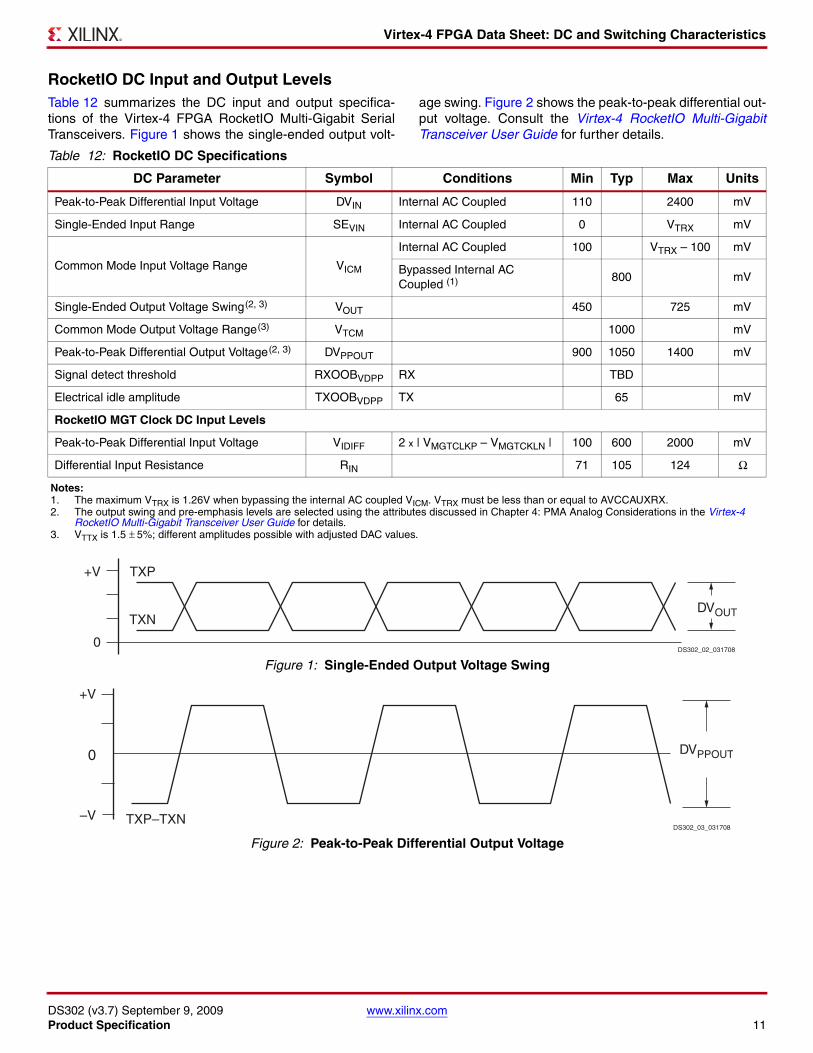
RocketIO DC Input and Output LevelsTable 12 summarizes the DC input and output specifica-tions of the Virtex-4 FPGA RocketIO Multi-Gigabit SerialTransceivers. Figure 1 shows the single-ended output volt-
age swing. Figure 2 shows the peak-to-peak differential out-put voltage. Consult the Virtex-4 RocketIO Multi-GigabitTransceiver User Guide for further details.
Table 12: RocketIO DC Specifications
DC Parameter Symbol Conditions Min Typ Max Units
Peak-to-Peak Differential Input Voltage DVIN Internal AC Coupled 110 2400 mV
Single-Ended Input Range SEVIN Internal AC Coupled 0 VTRX mV
Common Mode Input Voltage Range VICM
Internal AC Coupled 100 VTRX – 100 mV
Bypassed Internal AC Coupled (1) 800 mV
Single-Ended Output Voltage Swing(2, 3) VOUT 450 725 mV
Common Mode Output Voltage Range(3) VTCM 1000 mV
Peak-to-Peak Differential Output Voltage(2, 3) DVPPOUT 900 1050 1400 mV
Signal detect threshold RXOOBVDPP RX TBD
Electrical idle amplitude TXOOBVDPP TX 65 mV
RocketIO MGT Clock DC Input Levels
Peak-to-Peak Differential Input Voltage VIDIFF 2 x | VMGTCLKP – VMGTCKLN | 100 600 2000 mV
Differential Input Resistance RIN 71 105 124 Ω
Notes: 1. The maximum VTRX is 1.26V when bypassing the internal AC coupled VICM. VTRX must be less than or equal to AVCCAUXRX.2. The output swing and pre-emphasis levels are selected using the attributes discussed in Chapter 4: PMA Analog Considerations in the Virtex-4
RocketIO Multi-Gigabit Transceiver User Guide for details.3. VTTX is 1.5 ± 5%; different amplitudes possible with adjusted DAC values.
Figure 1: Single-Ended Output Voltage Swing
Figure 2: Peak-to-Peak Differential Output Voltage
0
+V TXP
TXN DVOUT
DS302_02_031708
0
+V
–V
TXP–TXN
DVPPOUT
DS302_03_031708

Virtex-4 FPGA Data Sheet: DC and Switching Characteristics
DS302 (v3.7) September 9, 2009 www.xilinx.comProduct Specification 12
Interface Performance Characteristics
Switching CharacteristicsSwitching characteristics are specified on a per-speed-grade basis and can be designated as Advance, Prelimi-nary, or Production. Each designation is defined as follows:
Advance
These specifications are based on simulations only and aretypically available soon after device design specificationsare frozen. Although speed grades with this designation areconsidered relatively stable and conservative, someunder-reporting might still occur.
Preliminary
These specifications are based on complete ES (engineer-ing sample) silicon characterization. Devices and speedgrades with this designation are intended to give a betterindication of the expected performance of production sili-con. The probability of under-reporting delays is greatlyreduced as compared to Advance data.
Production
These specifications are released once enough productionsilicon of a particular device family member has been char-acterized to provide full correlation between specificationsand devices over numerous production lots. There is nounder-reporting of delays, and customers receive formalnotification of any subsequent changes. Typically, the slow-est speed grades transition to Production before fasterspeed grades.
Table 14 correlates the current status of each Virtex-4device with a corresponding speed specification version1.68 designation.
Table 13: Interface Performance
Description
Speed Grade
-12 -11 -10
Networking Applications
SFI-4.1 (SDR LVDS Interface)(1) 710 MHz 710 MHz 645 MHz
SPI-4.2 (DDR LVDS Interface) 1 Gb/s 1 Gb/s 800 Mb/s
Memory Interfaces
DDR2 SDRAM (High-Performance SERDES Design)(2) 600 Mb/s 533 Mb/s 500 Mb/s
DDR2 SDRAM (Low-Latency Direct Clocking Design)(3) 420 Mb/s 410 Mb/s 400 Mb/s
QDRII SRAM (Low-Latency Direct Clocking Design)(4) 550 Mb/s 500 Mb/s 400 Mb/s
DDR SDRAM (Low-Latency Direct Clocking Design)(5) 344 Mb/s 336 Mb/s 330 Mb/s
RLDRAM II (Low-Latency Direct Clocking Design)(6) 470 Mb/s 470 Mb/s 400 Mb/s
Notes: 1. Input clocks above 622 MHz require AC coupling.2. Performance defined using design implementation described in application note XAPP721, High-Performance DDR2 SDRAM Interface Data
Capture Using ISERDES and OSERDES.3. Performance defined using design implementation described in application note XAPP702, DDR2 Controller Using Virtex-4 Devices.4. Performance defined using design implementation described in application note XAPP703, QDR II SRAM Interface for Virtex-4 Devices.5. Performance defined using design implementation described in application note XAPP709, DDR SDRAM Controller Using Virtex-4 FPGA Devices.6. Performance defined using design implementation described in application note XAPP710, Synthesizable CIO DDR RLDRAM II Controller for
Virtex-4 FPGAs.
Table 14: Virtex-4 Device Speed Grade Designations
Device
Speed Grade Designations
Advance Preliminary Production
XC4VLX15 -12, -11, -10
XC4VLX25 -12, -11, -10
XC4VLX40 -12, -11, -10
XC4VLX60 -12, -11, -10
XC4VLX80 -12, -11, -10
XC4VLX100 -12, -11, -10
XC4VLX160 -12, -11, -10
XC4VLX200 -11, -10
XC4VSX25 -12, -11, -10
XC4VSX35 -12, -11, -10
XC4VSX55 -12, -11, -10
XC4VFX12 -12, -11, -10
XC4VFX20 -12, -11, -10
XC4VFX40 -12, -11, -10
XC4VFX60 -12, -11, -10
XC4VFX100 -12, -11, -10
XC4VFX140 -11, -10

Virtex-4 FPGA Data Sheet: DC and Switching Characteristics
DS302 (v3.7) September 9, 2009 www.xilinx.comProduct Specification 13
Since individual family members are produced at differenttimes, the migration from one category to another dependscompletely on the status of the fabrication process for eachdevice.
All specifications are always representative of worst-casesupply voltage and junction temperature conditions.
Testing of Switching CharacteristicsAll devices are 100% functionally tested. Internal timingparameters are derived from measuring internal test pat-terns. Listed below are representative values. For morespecific, more precise, and worst-case guaranteed data,
use the values reported by the static timing analyzer (TRCEin the Xilinx Development System) and back-annotate to thesimulation net list. Unless otherwise noted, values apply toall Virtex-4 devices.
PowerPC Switching Characteristics
Consult the PowerPC 405 Processor Block Reference Guide for further information.
Table 15: PowerPC 405 Processor Clocks Absolute AC Characteristics
Description
Speed Grade
Units
-12 -11 -10
Min Max Min Max Min Max
Characteristics when APU Not Used
CPMC405CLOCK frequency(1,4) 0 450 0 400 0 350 MHz
CPMDCRCLK(3) 0 450 0 400 0 350 MHz
CPMFCMCLK(3) NA NA NA NA NA NA MHz
JTAGC405TCK frequency(2) 0 225 0 200 0 175 MHz
PLBCLK(3) 0 450 0 400 0 350 MHz
BRAMDSOCMCLK(3) 0 450 0 400 0 350 MHz
BRAMISOCMCLK(3) 0 450 0 400 0 350 MHz
Characteristics when APU Used
CPMC405CLOCK frequency(1,4) 0 333 0 275 0 233 MHz
CPMDCRCLK(3) 0 333 0 275 0 233 MHz
CPMFCMCLK(3) 0 333 0 275 0 233 MHz
JTAGC405TCK frequency(2) 0 166.5 0 137.5 0 116.5 MHz
PLBCLK(3) 0 333 0 275 0 233 MHz
BRAMDSOCMCLK(3) 0 333 0 275 0 233 MHz
BRAMISOCMCLK(3) 0 333 0 275 0 233 MHz
Notes: 1. Worst-case DCM output clock jitter is included in these specifications.2. The theoretical maximum frequency of this clock is one-half the CPMC405CLOCK. However, the achievable maximum is system dependent, and will
be much less.3. The theoretical maximum frequency of these clocks is equal to the CPMC405CLOCK. Integer clock ratios are required for the CPMC405CLOCK and
BRAMDSOCMCLK, CPMC405CLOCK and BRAMISOCMCLK, CPMC405CLOCK and CPMDCRCLK, CPMC405CLOCK and CPMFCMCLK, and CPMC405CLOCK and PLBCLK. The integer ratios can be different for each interface. However, the achievable maximum is system dependent.
4. Maximum operating frequency of CPMC405CLOCK is specified with the input pin TIEC405DISOPERANDFWD connected to a logic 1.
Virtex-4 FPGA Data Sheet: DC and Switching Characteristics
DS302 (v3.7) September 9, 2009 www.xilinx.comProduct Specification 14
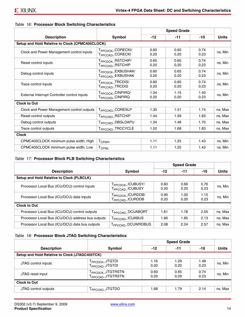
Table 16: Processor Block Switching Characteristics
Description Symbol
Speed Grade
Units-12 -11 -10
Setup and Hold Relative to Clock (CPMC405CLOCK)
Clock and Power Management control inputsTPPCDCK_CORECKI/TPPCCKD_CORECKI
0.600.20
0.650.20
0.740.23
ns, Min
Reset control inputsTPPCDCK_RSTCHIP/TPPCCKD_RSTCHIP
0.600.20
0.650.20
0.740.23
ns, Min
Debug control inputsTPPCDCK_EXBUSHAK/TPPCCKD_EXBUSHAK
0.600.20
0.650.20
0.740.23
ns, Min
Trace control inputsTPPCDCK_TRCDIS/TPPCCKD_TRCDIS
0.600.20
0.650.20
0.740.23
ns, Min
External Interrupt Controller control inputsTPPCDCK_CINPIRQ/TPPCCKD_CINPIRQ
1.040.20
1.150.20
1.400.23
ns, Min
Clock to Out
Clock and Power Management control outputs TPPCCKO_CORESLP 1.35 1.51 1.74 ns, Max
Reset control outputs TPPCCKO_RSTCHIP 1.44 1.59 1.83 ns, Max
Debug control outputs TPPCCKO_DBGLDAPU 1.34 1.48 1.70 ns, Max
Trace control outputs TPPCCKO_TRCCYCLE 1.52 1.68 1.83 ns, Max
Clock
CPMC405CLOCK minimum pulse width, High TCPWH 1.11 1.25 1.43 ns, Min
CPMC405CLOCK minimum pulse width, Low TCPWL 1.11 1.25 1.43 ns, Min
Table 17: Processor Block PLB Switching Characteristics
Description Symbol
Speed Grade
Units-12 -11 -10
Setup and Hold Relative to Clock (PLBCLK)
Processor Local Bus (ICU/DCU) control inputsTPPCDCK_ICUBUSY/TPPCCKD_ICUBUSY
0.600.20
0.660.20
0.760.23
ns, Min
Processor Local Bus (ICU/DCU) data inputsTPPCDCK_ICURDDB/TPPCCKD_ICURDDB
0.900.20
1.000.20
1.150.23
ns, Min
Clock to Out
Processor Local Bus (ICU/DCU) control outputs TPPCCKO_DCUABORT 1.61 1.78 2.05 ns, Max
Processor Local Bus (ICU/DCU) address bus outputs TPPCCKO_ICUABUS 1.66 1.85 2.13 ns, Max
Processor Local Bus (ICU/DCU) data bus outputs TPPCCKO_DCUWRDBUS 2.08 2.24 2.57 ns, Max
Table 18: Processor Block JTAG Switching Characteristics
Description Symbol
Speed Grade
Units-12 -11 -10
Setup and Hold Relative to Clock (JTAGC405TCK)
JTAG control inputsTPPCDCK_JTGTDITPPCCKD_JTGTDI
1.160.20
1.290.20
1.480.23
ns, Min
JTAG reset inputTPPCDCK_JTGTRSTNTPPCCKD_JTGTRSTN
0.600.20
0.650.20
0.740.23
ns, Min
Clock to Out
JTAG control outputs TPPCCKO_JTGTDO 1.68 1.79 2.14 ns, Max

Virtex-4 FPGA Data Sheet: DC and Switching Characteristics
DS302 (v3.7) September 9, 2009 www.xilinx.comProduct Specification 15
Table 19: PowerPC 405 Data-Side On-Chip Memory Switching Characteristics
Description Symbol
Speed Grade
Units-12 -11 -10
Setup and Hold Relative to Clock (BRAMDSOCMCLK)
Data-Side On-Chip Memory data bus inputsTPPCDCK_DSOCMRDDBTPPCCKD_DSOCMRDDB
0.600.20
0.650.20
0.740.23
ns, Min
Clock to Out
Data-Side On-Chip Memory control outputs TPPCCKO_BRAMBWR 2.07 2.30 2.65 ns, Max
Data-Side On-Chip Memory address bus outputs TPPCCKO_BRAMABUS 2.07 2.30 2.65 ns, Max
Data-Side On-Chip Memory data bus outputs TPPCCKO_IBRAMWRDBUS01 1.61 1.79 2.06 ns, Max
Table 20: PowerPC 405 Instruction-Side On-Chip Memory Switching Characteristics
Description Symbol
Speed Grade
Units-12 -11 -10
Setup and Hold Relative to Clock (BRAMISOCMCLK)
Instruction-Side On-Chip Memory data bus inputsTPPCDCK_ISOCMRDDBTPPCCKD_ISOCMRDDB
0.740.20
0.820.20
0.940.23
ns, Min
Clock to Out
Instruction-Side On-Chip Memory control outputs TPPCCKO_IBRAMEN 3.04 3.37 3.88 ns, Max
Instruction-Side On-Chip Memory address bus outputs TPPCCKO_IBRAMRDABUS 1.67 1.85 2.13 ns, Max
Instruction-Side On-Chip Memory data bus outputs TPPCCKO_IBRAMWRDBUS 1.67 1.86 2.14 ns, Max
Table 21: Processor Block DCR Bus Switching Characteristics
Description Symbol
Speed Grade
Units-12 -11 -10
Setup and Hold Relative to Clock (CPMDCRCLOCK)
Device Control Register Bus control inputsTPPCDCK_EXDCRACKTPPCCKD_EXDCRACK
0.120.15
0.130.17
0.150.19
ns, Min
Device Control Register Bus data inputsTPPCDCK_EXDCRDBUSITPPCCKD_EXDCRDBUSI
0.570.16
0.570.16
1.020.27
ns, Min
Clock to Out
Device Control Register Bus control outputs TPPCCKO_EXDCRRD 1.20 1.35 1.54 ns, Max
Device Control Register Bus address bus outputs TPPCCKO_EXDCRABUS 1.28 1.45 1.66 ns, Max
Device Control Register Bus data bus outputs TPPCCKO_EXDCRDBUSO 1.31 1.45 1.67 ns, Max
Virtex-4 FPGA Data Sheet: DC and Switching Characteristics
DS302 (v3.7) September 9, 2009 www.xilinx.comProduct Specification 16
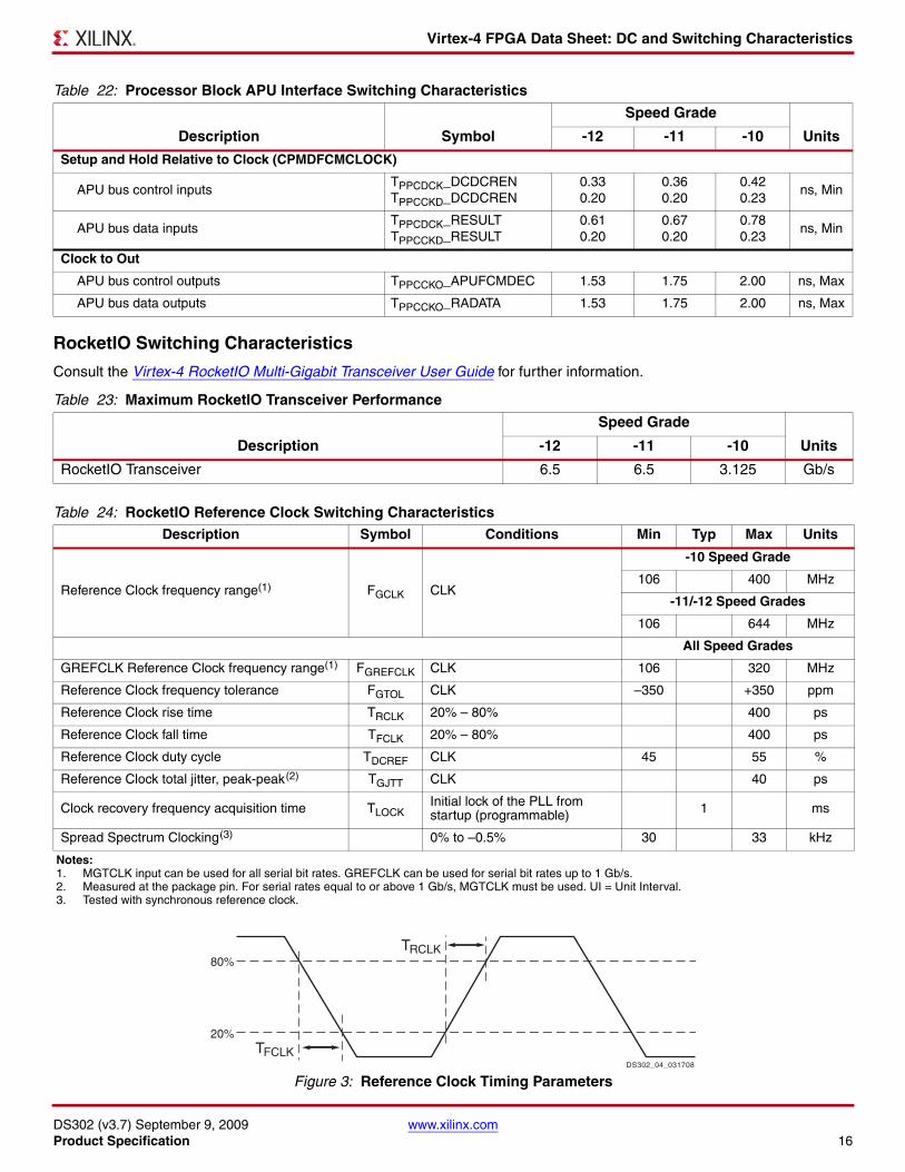
RocketIO Switching Characteristics
Consult the Virtex-4 RocketIO Multi-Gigabit Transceiver User Guide for further information.
Table 22: Processor Block APU Interface Switching Characteristics
Description Symbol
Speed Grade
Units-12 -11 -10
Setup and Hold Relative to Clock (CPMDFCMCLOCK)
APU bus control inputsTPPCDCK_DCDCRENTPPCCKD_DCDCREN
0.330.20
0.360.20
0.420.23
ns, Min
APU bus data inputsTPPCDCK_RESULTTPPCCKD_RESULT
0.610.20
0.670.20
0.780.23
ns, Min
Clock to Out
APU bus control outputs TPPCCKO_APUFCMDEC 1.53 1.75 2.00 ns, Max
APU bus data outputs TPPCCKO_RADATA 1.53 1.75 2.00 ns, Max
Table 23: Maximum RocketIO Transceiver Performance
Description
Speed Grade
Units-12 -11 -10
RocketIO Transceiver 6.5 6.5 3.125 Gb/s
Table 24: RocketIO Reference Clock Switching CharacteristicsDescription Symbol Conditions Min Typ Max Units
Reference Clock frequency range(1) FGCLK CLK
-10 Speed Grade
106 400 MHz
-11/-12 Speed Grades
106 644 MHz
All Speed Grades
GREFCLK Reference Clock frequency range(1) FGREFCLK CLK 106 320 MHz
Reference Clock frequency tolerance FGTOL CLK –350 +350 ppm
Reference Clock rise time TRCLK 20% – 80% 400 ps
Reference Clock fall time TFCLK 20% – 80% 400 ps
Reference Clock duty cycle TDCREF CLK 45 55 %
Reference Clock total jitter, peak-peak(2) TGJTT CLK 40 ps
Clock recovery frequency acquisition time TLOCKInitial lock of the PLL from startup (programmable) 1 ms
Spread Spectrum Clocking(3) 0% to –0.5% 30 33 kHz
Notes: 1. MGTCLK input can be used for all serial bit rates. GREFCLK can be used for serial bit rates up to 1 Gb/s.2. Measured at the package pin. For serial rates equal to or above 1 Gb/s, MGTCLK must be used. UI = Unit Interval.3. Tested with synchronous reference clock.
Figure 3: Reference Clock Timing ParametersDS302_04_031708
80%
20% T FCLK
T RCLK

Virtex-4 FPGA Data Sheet: DC and Switching Characteristics
DS302 (v3.7) September 9, 2009 www.xilinx.comProduct Specification 17
Table 25: RocketIO Receiver Switching Characteristics
Description Symbol Conditions Min Typ Max Units
Serial data rate, -10 FGRX 0.622 3.125 Gb/s
Serial data rate, -11 FGRX 0.622 6.5 Gb/s
XAUI Receive Jitter Tolerance (8B/10B CJPAT) (2) Rate (Gb/s) Mode(3) Frequency
Receive Deterministic Jitter Tolerance TDJTOL 3.125 ACDR 0.37
UI(1)
Receive Total Jitter Tolerance TTJTOL(6) 3.125 ACDR 0.65
Receive Sinusoidal Jitter Tolerance TSJTOL(7)
3.125 ACDR f = 22.1 kHz 8.5
3.125 ACDR f = 1.875 MHz 0.10
3.125 ACDR f = 20 MHz 0.10
General Receive Jitter Tolerance Rate (Gb/s) Mode(3) Pattern
Receive deterministic jitter tolerance TDJTOL(2,4)
6.5(5) ACDR PRBS7 0.65
UI(1)
5.0(5) ACDR PRBS7 0.65
4.25(5) ACDR PRBS7 0.65
3.125 ACDR PRBS7 0.60
2.5 ACDR PRBS7 0.55
1.25 ACDR PRBS7 0.50
1.25 DCDR PRBS7 0.50
1.25 DCDR PRBS31 0.40
0.622 DCDR PRBS31 0.40
Sinusoidal jitter tolerance TSJTOL
6.5(9) ACDR PRBS7 0.65
5.0(9) ACDR PRBS7 0.65
4.25(9) ACDR PRBS7 0.65
3.125(8) ACDR PRBS7 0.50
2.5(8) ACDR PRBS7 0.50
1.25(8) ACDR PRBS7 0.50
1.25(8) DCDR PRBS7 0.55
1.25(8) DCDR PRBS31 0.35
0.622(8) DCDR PRBS31 0.55
RXUSRCLK frequency TRX For slower speed grades = MaxDataRate/32 250 MHz
RXUSRCLK2 frequency TRX2 250 MHz
RXUSRCLK duty cycle TRXDC 40 60 %
RXUSRCLK2 duty cycle TRX2DC 40 60 %
Differential input skew TISKEW 20 ps
Differential receive input sensitivity(2) VEYE 110 mV
On-chip AC coupling corner frequency
Signal detect response time RXSIGDETResponsetime 30 ns
Input capacitance at the Die CDIE fF
Excess capacitance at the solder ball CBALL fF
Notes: 1. UI = Unit Interval2. Using receiver equalization setting of 111 (14 dB).3. ACDR = Analog CDR and DCDR = Digital CDR.4. Deterministic jitter (DJ) is composed of 75% ISI + 25% high frequency
sinusoidal jitter (SJ).5. Deterministic Jitter (DJ) composed of ISI + 0.10 UI of high frequency SJ +
0.15 UI of RJ.
6. Sum of DJ, random jitter (RJ) of at least 0.55 UI, and sinusoidal jitter as defined by mask in IEEE Std 802.3ae-2002, Figure 47-5.
7. SJ in addition to 0.55 UI of DJ +RJ.8. Jitter frequency = 5 MHz.9. Jitter frequency = 10 MHz.

Virtex-4 FPGA Data Sheet: DC and Switching Characteristics
DS302 (v3.7) September 9, 2009 www.xilinx.comProduct Specification 18
Table 26: RocketIO Transmitter Switching Characteristics
Description Symbol Conditions Min Typ Max Units
Serial data rate, -10 FGTX 0.622 3.125 Gb/s
Serial data rate, -11 FGTX 0.622 6.5 Gb/s
Data Rate (Gb/s)
TX Jitter Generation(3)
TJ
PRBS7 6.5
0.50
UI(1)
RJ 0.35
DJ 0.30
TJ
PRBS7 5.0
0.45
RJ 0.30
DJ 0.25
TJ
PRBS7 4.25
0.40
RJ 0.25
DJ 0.21
TJ
PRBS7 3.125
0.28
RJ 0.14
DJ 0.14
TJ
PRBS7 2.5
0.25
RJ 0.18
DJ 0.12
TJ
PRBS7 1.25
0.12
RJ 0.10
DJ 0.06
TJ
PRBS31 0.622
0.08
RJ 0.06
DJ 0.04
TX rise time(2) TRTX 20% – 80% 90 ps
TX fall time(2) TFTX 20% – 80% 90 ps
TXUSRCLK frequencyFor slower speed grades = MaxDataRate/32
250 MHz
TXUSRCLK2 frequency 250 MHz
TXUSRCLK duty cycle TTXDC 40 60 %
TXUSRCLK2 duty cycle TTX2DC 40 60 %
Differential output skew TISKEW 12 20 ps
Electrical idle transition time TXOOBTransition 15 ns
Notes: 1. UI = Unit Interval.2. Default attributes, measured at 2.5 Gb/s.3. Peak-to-Peak values measured relative to 1e-12 Error rate. Default attributes. TX feedback divider (TXPLLNDIVSEL) = 10.
Virtex-4 FPGA Data Sheet: DC and Switching Characteristics
DS302 (v3.7) September 9, 2009 www.xilinx.comProduct Specification 19
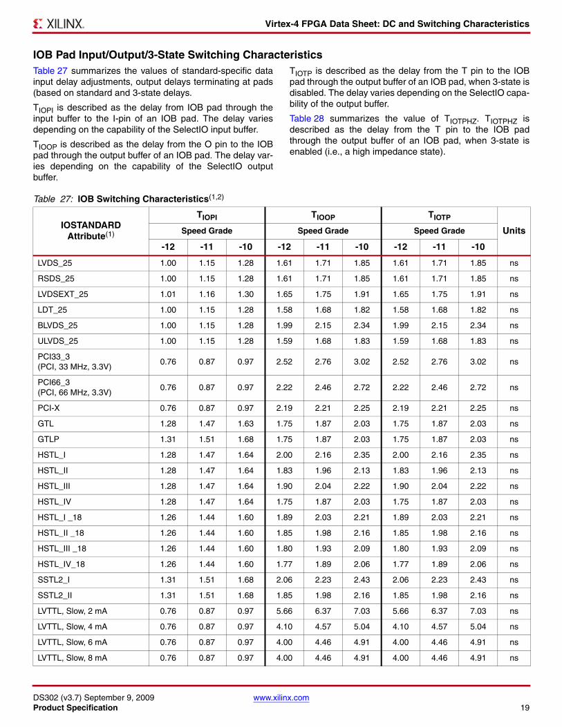
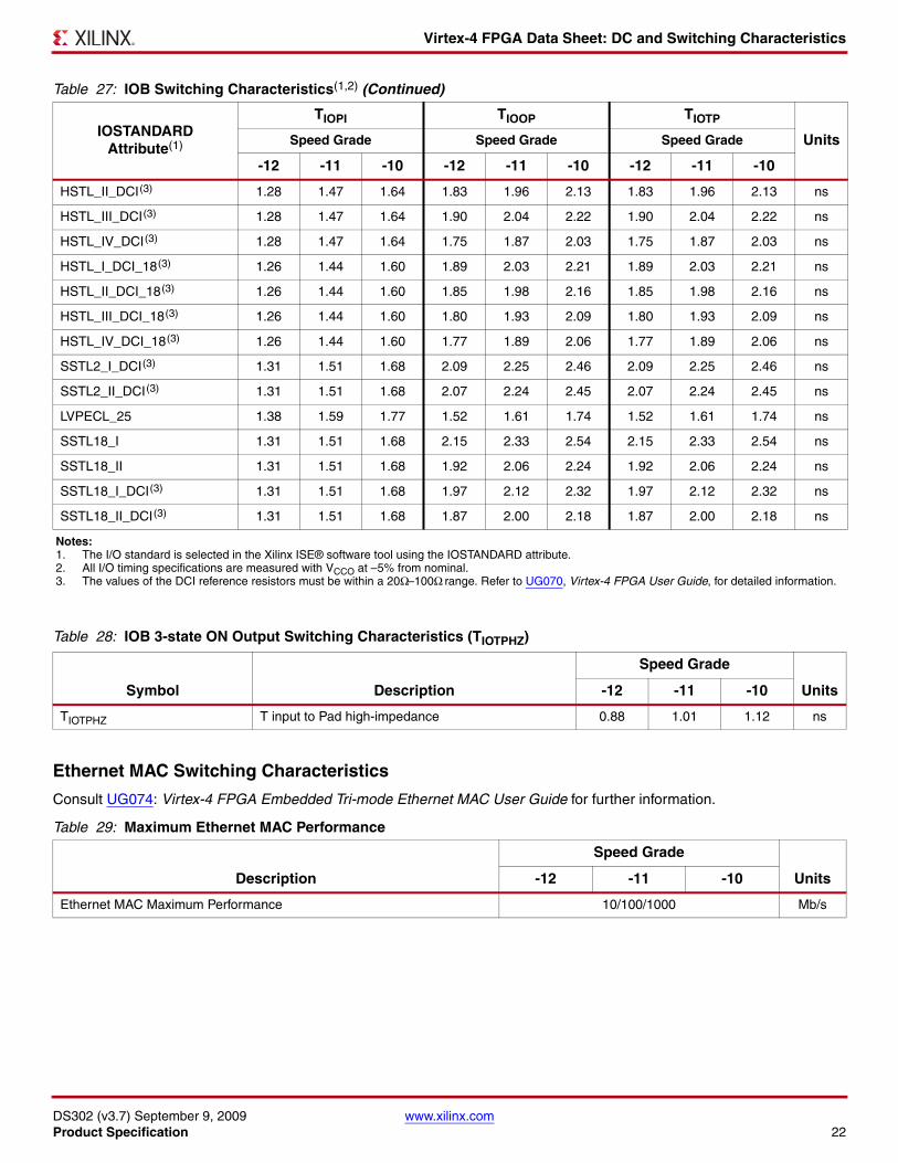
IOB Pad Input/Output/3-State Switching CharacteristicsTable 27 summarizes the values of standard-specific datainput delay adjustments, output delays terminating at pads(based on standard and 3-state delays.
TIOPI is described as the delay from IOB pad through theinput buffer to the I-pin of an IOB pad. The delay variesdepending on the capability of the SelectIO input buffer.
TIOOP is described as the delay from the O pin to the IOBpad through the output buffer of an IOB pad. The delay var-ies depending on the capability of the SelectIO outputbuffer.
TIOTP is described as the delay from the T pin to the IOBpad through the output buffer of an IOB pad, when 3-state isdisabled. The delay varies depending on the SelectIO capa-bility of the output buffer.
Table 28 summarizes the value of TIOTPHZ. TIOTPHZ isdescribed as the delay from the T pin to the IOB padthrough the output buffer of an IOB pad, when 3-state isenabled (i.e., a high impedance state).
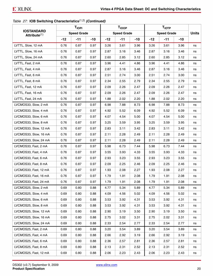
Table 27: IOB Switching Characteristics(1,2)
IOSTANDARD Attribute(1)
TIOPI TIOOP TIOTP
UnitsSpeed Grade Speed Grade Speed Grade
-12 -11 -10 -12 -11 -10 -12 -11 -10
LVDS_25 1.00 1.15 1.28 1.61 1.71 1.85 1.61 1.71 1.85 ns
RSDS_25 1.00 1.15 1.28 1.61 1.71 1.85 1.61 1.71 1.85 ns
LVDSEXT_25 1.01 1.16 1.30 1.65 1.75 1.91 1.65 1.75 1.91 ns
LDT_25 1.00 1.15 1.28 1.58 1.68 1.82 1.58 1.68 1.82 ns
BLVDS_25 1.00 1.15 1.28 1.99 2.15 2.34 1.99 2.15 2.34 ns
ULVDS_25 1.00 1.15 1.28 1.59 1.68 1.83 1.59 1.68 1.83 ns
PCI33_3 (PCI, 33 MHz, 3.3V)
0.76 0.87 0.97 2.52 2.76 3.02 2.52 2.76 3.02 ns
PCI66_3(PCI, 66 MHz, 3.3V)
0.76 0.87 0.97 2.22 2.46 2.72 2.22 2.46 2.72 ns
PCI-X 0.76 0.87 0.97 2.19 2.21 2.25 2.19 2.21 2.25 ns
GTL 1.28 1.47 1.63 1.75 1.87 2.03 1.75 1.87 2.03 ns
GTLP 1.31 1.51 1.68 1.75 1.87 2.03 1.75 1.87 2.03 ns
HSTL_I 1.28 1.47 1.64 2.00 2.16 2.35 2.00 2.16 2.35 ns
HSTL_II 1.28 1.47 1.64 1.83 1.96 2.13 1.83 1.96 2.13 ns
HSTL_III 1.28 1.47 1.64 1.90 2.04 2.22 1.90 2.04 2.22 ns
HSTL_IV 1.28 1.47 1.64 1.75 1.87 2.03 1.75 1.87 2.03 ns
HSTL_I _18 1.26 1.44 1.60 1.89 2.03 2.21 1.89 2.03 2.21 ns
HSTL_II _18 1.26 1.44 1.60 1.85 1.98 2.16 1.85 1.98 2.16 ns
HSTL_III _18 1.26 1.44 1.60 1.80 1.93 2.09 1.80 1.93 2.09 ns
HSTL_IV_18 1.26 1.44 1.60 1.77 1.89 2.06 1.77 1.89 2.06 ns
SSTL2_I 1.31 1.51 1.68 2.06 2.23 2.43 2.06 2.23 2.43 ns
SSTL2_II 1.31 1.51 1.68 1.85 1.98 2.16 1.85 1.98 2.16 ns
LVTTL, Slow, 2 mA 0.76 0.87 0.97 5.66 6.37 7.03 5.66 6.37 7.03 ns
LVTTL, Slow, 4 mA 0.76 0.87 0.97 4.10 4.57 5.04 4.10 4.57 5.04 ns
LVTTL, Slow, 6 mA 0.76 0.87 0.97 4.00 4.46 4.91 4.00 4.46 4.91 ns
LVTTL, Slow, 8 mA 0.76 0.87 0.97 4.00 4.46 4.91 4.00 4.46 4.91 ns
Virtex-4 FPGA Data Sheet: DC and Switching Characteristics
DS302 (v3.7) September 9, 2009 www.xilinx.comProduct Specification 20
LVTTL, Slow, 12 mA 0.76 0.87 0.97 3.26 3.61 3.96 3.26 3.61 3.96 ns
LVTTL, Slow, 16 mA 0.76 0.87 0.97 2.87 3.16 3.46 2.87 3.16 3.46 ns
LVTTL, Slow, 24 mA 0.76 0.87 0.97 2.60 2.85 3.12 2.60 2.85 3.12 ns
LVTTL, Fast, 2 mA 0.76 0.87 0.97 3.96 4.41 4.86 3.96 4.41 4.86 ns
LVTTL, Fast, 4 mA 0.76 0.87 0.97 2.87 3.16 3.46 2.87 3.16 3.46 ns
LVTTL, Fast, 6 mA 0.76 0.87 0.97 2.51 2.74 3.00 2.51 2.74 3.00 ns
LVTTL, Fast, 8 mA 0.76 0.87 0.97 2.34 2.55 2.79 2.34 2.55 2.79 ns
LVTTL, Fast, 12 mA 0.76 0.87 0.97 2.09 2.26 2.47 2.09 2.26 2.47 ns
LVTTL, Fast, 16 mA 0.76 0.87 0.97 2.09 2.26 2.47 2.09 2.26 2.47 ns
LVTTL, Fast, 24 mA 0.76 0.87 0.97 1.88 2.02 2.20 1.88 2.02 2.20 ns
LVCMOS33, Slow, 2 mA 0.76 0.87 0.97 6.98 7.88 8.73 6.98 7.88 8.73 ns
LVCMOS33, Slow, 4 mA 0.76 0.87 0.97 4.92 5.52 6.09 4.92 5.52 6.09 ns
LVCMOS33, Slow, 6 mA 0.76 0.87 0.97 4.07 4.54 5.00 4.07 4.54 5.00 ns
LVCMOS33, Slow, 8 mA 0.76 0.87 0.97 3.25 3.59 3.95 3.25 3.59 3.95 ns
LVCMOS33, Slow, 12 mA 0.76 0.87 0.97 2.83 3.11 3.42 2.83 3.11 3.42 ns
LVCMOS33, Slow, 16 mA 0.76 0.87 0.97 2.11 2.28 2.49 2.11 2.28 2.49 ns
LVCMOS33, Slow, 24 mA 0.76 0.87 0.97 2.11 2.28 2.49 2.11 2.28 2.49 ns
LVCMOS33, Fast, 2 mA 0.76 0.87 0.97 5.98 6.73 7.44 5.98 6.73 7.44 ns
LVCMOS33, Fast, 4 mA 0.76 0.87 0.97 3.55 3.93 4.33 3.55 3.93 4.33 ns
LVCMOS33, Fast, 6 mA 0.76 0.87 0.97 2.93 3.23 3.55 2.93 3.23 3.55 ns
LVCMOS33, Fast, 8 mA 0.76 0.87 0.97 2.09 2.25 2.46 2.09 2.25 2.46 ns
LVCMOS33, Fast, 12 mA 0.76 0.87 0.97 1.93 2.08 2.27 1.93 2.08 2.27 ns
LVCMOS33, Fast, 16 mA 0.76 0.87 0.97 1.79 1.91 2.08 1.79 1.91 2.08 ns
LVCMOS33, Fast, 24 mA 0.76 0.87 0.97 1.79 1.91 2.08 1.79 1.91 2.08 ns
LVCMOS25, Slow, 2 mA 0.69 0.80 0.88 4.77 5.34 5.89 4.77 5.34 5.89 ns
LVCMOS25, Slow, 4 mA 0.69 0.80 0.88 4.09 4.56 5.02 4.09 4.56 5.02 ns
LVCMOS25, Slow, 6 mA 0.69 0.80 0.88 3.53 3.92 4.31 3.53 3.92 4.31 ns
LVCMOS25, Slow, 8 mA 0.69 0.80 0.88 3.53 3.92 4.31 3.53 3.92 4.31 ns
LVCMOS25, Slow, 12 mA 0.69 0.80 0.88 2.90 3.19 3.50 2.90 3.19 3.50 ns
LVCMOS25, Slow, 16 mA 0.69 0.80 0.88 2.75 3.02 3.31 2.75 2.02 3.31 ns
LVCMOS25, Slow, 24 mA 0.69 0.80 0.88 2.33 2.54 2.77 2.33 2.54 2.77 ns
LVCMOS25, Fast, 2 mA 0.69 0.80 0.88 3.20 3.54 3.89 3.20 3.54 3.89 ns
LVCMOS25, Fast, 4 mA 0.69 0.80 0.88 2.66 2.92 3.19 2.66 2.92 3.19 ns
LVCMOS25, Fast, 6 mA 0.69 0.80 0.88 2.36 2.57 2.81 2.36 2.57 2.81 ns
LVCMOS25, Fast, 8 mA 0.69 0.80 0.88 2.13 2.31 2.52 2.13 2.31 2.52 ns
LVCMOS25, Fast, 12 mA 0.69 0.80 0.88 2.06 2.23 2.43 2.06 2.23 2.43 ns
Table 27: IOB Switching Characteristics(1,2) (Continued)
IOSTANDARD Attribute(1)
TIOPI TIOOP TIOTP
UnitsSpeed Grade Speed Grade Speed Grade
-12 -11 -10 -12 -11 -10 -12 -11 -10

Virtex-4 FPGA Data Sheet: DC and Switching Characteristics
DS302 (v3.7) September 9, 2009 www.xilinx.comProduct Specification 21
LVCMOS25, Fast, 16 mA 0.69 0.80 0.88 1.89 2.03 2.21 1.89 2.03 2.21 ns
LVCMOS25, Fast, 24 mA 0.69 0.80 0.88 1.83 1.96 2.13 1.83 1.96 2.13 ns
LVCMOS18, Slow, 2 mA 0.97 1.12 1.25 4.77 5.34 5.89 4.77 5.34 5.89 ns
LVCMOS18, Slow, 4 mA 0.97 1.12 1.25 3.56 3.95 4.35 3.56 3.95 4.35 ns
LVCMOS18, Slow, 6 mA 0.97 1.12 1.25 3.29 3.64 4.00 3.29 3.64 4.00 ns
LVCMOS18, Slow, 8 mA 0.97 1.12 1.25 3.10 3.42 3.76 3.10 3.42 3.76 ns
LVCMOS18, Slow, 12 mA 0.97 1.12 1.25 3.09 3.41 3.74 3.09 3.41 3.74 ns
LVCMOS18, Slow, 16 mA 0.97 1.12 1.25 2.94 3.24 3.55 2.94 3.24 3.55 ns
LVCMOS18, Fast, 2 mA 0.97 1.12 1.25 3.20 3.54 3.89 3.20 3.54 3.89 ns
LVCMOS18, Fast, 4 mA 0.97 1.12 1.25 2.52 2.75 3.02 2.52 2.75 3.02 ns
LVCMOS18, Fast, 6 mA 0.97 1.12 1.25 2.29 2.49 2.72 2.29 2.49 2.72 ns
LVCMOS18, Fast, 8 mA 0.97 1.12 1.25 2.13 2.31 2.52 2.13 2.31 2.52 ns
LVCMOS18, Fast, 12 mA 0.97 1.12 1.25 2.01 2.17 2.36 2.01 2.17 2.36 ns
LVCMOS18, Fast, 16 mA 0.97 1.12 1.25 1.94 2.09 2.27 1.94 2.09 2.27 ns
LVCMOS15, Slow, 2 mA 1.05 1.20 1.34 5.33 5.99 6.61 5.33 5.99 6.61 ns
LVCMOS15, Slow, 4 mA 1.05 1.20 1.34 4.21 4.70 4.88 4.21 4.70 4.88 ns
LVCMOS15, Slow, 6 mA 1.05 1.20 1.34 3.49 3.87 4.26 3.49 3.87 4.26 ns
LVCMOS15, Slow, 8 mA 1.05 1.20 1.34 3.49 3.87 4.26 3.49 3.87 4.26 ns
LVCMOS15, Slow, 12 mA 1.05 1.20 1.34 3.11 3.43 3.77 3.11 3.43 3.77 ns
LVCMOS15, Slow, 16 mA 1.05 1.20 1.34 2.92 3.21 3.53 2.92 3.21 3.53 ns
LVCMOS15, Fast, 2 mA 1.05 1.20 1.34 3.42 3.79 4.17 3.42 3.79 4.17 ns
LVCMOS15, Fast, 4 mA 1.05 1.20 1.34 2.76 3.03 3.32 2.76 3.03 3.32 ns
LVCMOS15, Fast, 6 mA 1.05 1.20 1.34 2.46 2.69 2.94 2.46 2.69 2.94 ns
LVCMOS15, Fast, 8 mA 1.05 1.20 1.34 2.28 2.48 2.71 2.28 2.48 2.71 ns
LVCMOS15, Fast, 12 mA 1.05 1.20 1.34 2.12 2.29 2.50 2.12 2.29 2.50 ns
LVCMOS15, Fast, 16 mA 1.05 1.20 1.34 2.06 2.23 2.43 2.06 2.23 2.43 ns
LVDCI_33 0.76 0.87 0.97 2.61 2.86 3.13 2.61 2.86 3.13 ns
LVDCI_25 0.69 0.80 0.88 2.52 2.76 3.02 2.52 2.76 3.02 ns
LVDCI_18 0.97 1.12 1.25 2.47 2.69 2.95 2.47 2.69 2.95 ns
LVDCI_15 1.05 1.20 1.34 2.45 2.68 2.93 2.45 2.68 2.93 ns
LVDCI_DV2_25 0.69 0.80 0.88 1.93 2.08 2.27 1.93 2.08 2.27 ns
LVDCI_DV2_18 0.97 1.12 1.25 1.95 2.09 2.28 1.95 2.09 2.28 ns
LVDCI_DV2_15 1.05 1.20 1.34 2.18 2.36 2.58 2.18 2.36 2.58 ns
GTL_DCI(3) 1.18 1.36 1.51 1.75 1.87 2.03 1.75 1.87 2.03 ns
GTLP_DCI(3) 0.96 1.11 1.23 1.75 1.87 2.03 1.75 1.87 2.03 ns
HSTL_I_DCI(3) 1.28 1.47 1.64 2.00 2.16 2.35 2.00 2.16 2.35 ns
Table 27: IOB Switching Characteristics(1,2) (Continued)
IOSTANDARD Attribute(1)
TIOPI TIOOP TIOTP
UnitsSpeed Grade Speed Grade Speed Grade
-12 -11 -10 -12 -11 -10 -12 -11 -10
Virtex-4 FPGA Data Sheet: DC and Switching Characteristics
DS302 (v3.7) September 9, 2009 www.xilinx.comProduct Specification 22
Ethernet MAC Switching Characteristics
Consult UG074: Virtex-4 FPGA Embedded Tri-mode Ethernet MAC User Guide for further information.
HSTL_II_DCI(3) 1.28 1.47 1.64 1.83 1.96 2.13 1.83 1.96 2.13 ns
HSTL_III_DCI(3) 1.28 1.47 1.64 1.90 2.04 2.22 1.90 2.04 2.22 ns
HSTL_IV_DCI(3) 1.28 1.47 1.64 1.75 1.87 2.03 1.75 1.87 2.03 ns
HSTL_I_DCI_18(3) 1.26 1.44 1.60 1.89 2.03 2.21 1.89 2.03 2.21 ns
HSTL_II_DCI_18(3) 1.26 1.44 1.60 1.85 1.98 2.16 1.85 1.98 2.16 ns
HSTL_III_DCI_18(3) 1.26 1.44 1.60 1.80 1.93 2.09 1.80 1.93 2.09 ns
HSTL_IV_DCI_18(3) 1.26 1.44 1.60 1.77 1.89 2.06 1.77 1.89 2.06 ns
SSTL2_I_DCI(3) 1.31 1.51 1.68 2.09 2.25 2.46 2.09 2.25 2.46 ns
SSTL2_II_DCI(3) 1.31 1.51 1.68 2.07 2.24 2.45 2.07 2.24 2.45 ns
LVPECL_25 1.38 1.59 1.77 1.52 1.61 1.74 1.52 1.61 1.74 ns
SSTL18_I 1.31 1.51 1.68 2.15 2.33 2.54 2.15 2.33 2.54 ns
SSTL18_II 1.31 1.51 1.68 1.92 2.06 2.24 1.92 2.06 2.24 ns
SSTL18_I_DCI(3) 1.31 1.51 1.68 1.97 2.12 2.32 1.97 2.12 2.32 ns
SSTL18_II_DCI(3) 1.31 1.51 1.68 1.87 2.00 2.18 1.87 2.00 2.18 ns
Notes: 1. The I/O standard is selected in the Xilinx ISE® software tool using the IOSTANDARD attribute.2. All I/O timing specifications are measured with VCCO at –5% from nominal.3. The values of the DCI reference resistors must be within a 20Ω–100Ω range. Refer to UG070, Virtex-4 FPGA User Guide, for detailed information.
Table 27: IOB Switching Characteristics(1,2) (Continued)
IOSTANDARD Attribute(1)
TIOPI TIOOP TIOTP
UnitsSpeed Grade Speed Grade Speed Grade
-12 -11 -10 -12 -11 -10 -12 -11 -10
Table 28: IOB 3-state ON Output Switching Characteristics (TIOTPHZ)
Symbol Description
Speed Grade
Units-12 -11 -10
TIOTPHZ T input to Pad high-impedance 0.88 1.01 1.12 ns
Table 29: Maximum Ethernet MAC Performance
Description
Speed Grade
Units-12 -11 -10
Ethernet MAC Maximum Performance 10/100/1000 Mb/s

Virtex-4 FPGA Data Sheet: DC and Switching Characteristics
DS302 (v3.7) September 9, 2009 www.xilinx.comProduct Specification 23
I/O Standard Adjustment Measurement Methodology
Input Delay Measurements
Table 30 shows the test setup parameters used for measuring input delay.
Table 30: Input Delay Measurement Methodology
DescriptionI/O Standard
Attribute VL(1,2) VH
(1,2)VMEAS (1,4,5)
VREF (1,3,5)
LVTTL (Low-Voltage Transistor-Transistor Logic) LVTTL 0 3.0 1.4 –
LVCMOS (Low-Voltage CMOS), 3.3V LVCMOS33 0 3.3 1.65 –
LVCMOS, 2.5V LVCMOS25 0 2.5 1.25 –
LVCMOS, 1.8V LVCMOS18 0 1.8 0.9 –
LVCMOS, 1.5V LVCMOS15 0 1.5 0.75 –
PCI (Peripheral Component Interface), 33 MHz, 3.3V
PCI33_3 Per PCI™ Specification –
PCI, 66 MHz, 3.3V PCI66_3 Per PCI Specification –
PCI-X, 133 MHz, 3.3V PCIX Per PCI-X™ Specification –
GTL (Gunning Transceiver Logic) GTL VREF – 0.2 VREF + 0.2 VREF 0.80
GTL Plus GTLP VREF – 0.2 VREF + 0.2 VREF 1.0
HSTL (High-Speed Transceiver Logic), Class I & II
HSTL_I, HSTL_II VREF – 0.5 VREF + 0.5 VREF 0.75
HSTL, Class III & IV HSTL_III, HSTL_IV VREF – 0.5 VREF + 0.5 VREF 0.90
HSTL, Class I & II, 1.8V HSTL_I_18, HSTL_II_18 VREF – 0.5 VREF + 0.5 VREF 0.90
HSTL, Class III & IV, 1.8VHSTL_III_18, HSTL_IV_18
VREF – 0.5 VREF + 0.5 VREF 1.08
SSTL (Stub Terminated Transceiver Logic), Class I & II, 3.3V
SSTL3_I, SSTL3_II VREF – 1.00 VREF + 1.00 VREF 1.5
SSTL, Class I & II, 2.5V SSTL2_I, SSTL2_II VREF – 0.75 VREF + 0.75 VREF 1.25
SSTL, Class I & II, 1.8V SSTL18_I, SSTL18_II VREF – 0.5 VREF + 0.5 VREF 0.90
AGP-2X/AGP (Accelerated Graphics Port) AGPVREF –
(0.2 xVCCO)VREF +
(0.2 xVCCO)VREF
AGP Spec
LVDS (Low-Voltage Differential Signaling), 2.5V LVDS_25 1.2 – 0.125 1.2 + 0.125 1.2
LVDSEXT (LVDS Extended Mode), 2.5V LVDSEXT_25 1.2 – 0.125 1.2 + 0.125 1.2
ULVDS (Ultra LVDS), 2.5V ULVDS_25 0.6 – 0.125 0.6 + 0.125 0.6
LDT (HyperTransport), 2.5V LDT_25 0.6 – 0.125 0.6 + 0.125 0.6
Notes: 1. Input delay measurement methodology parameters for LVDCI and HSLVDCI are the same as for LVCMOS standards of the same voltage.
Parameters for all other DCI standards are the same as for the corresponding non-DCI standards.2. Input waveform switches between VLand VH.3. Measurements are made at typical, minimum, and maximum VREF values. Reported delays reflect worst case of these measurements. VREF values
listed are typical.4. Input voltage level from which measurement starts. 5. This is an input voltage reference that bears no relation to the VREF / VMEAS parameters found in IBIS models and/or noted in Figure 4.
Virtex-4 FPGA Data Sheet: DC and Switching Characteristics
DS302 (v3.7) September 9, 2009 www.xilinx.comProduct Specification 24
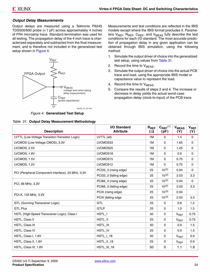
Output Delay Measurements
Output delays are measured using a Tektronix P6245TDS500/600 probe (< 1 pF) across approximately 4 inchesof FR4 microstrip trace. Standard termination was used forall testing. The propagation delay of the 4 inch trace is char-acterized separately and subtracted from the final measure-ment, and is therefore not included in the generalized testsetup shown in Figure 4.
Measurements and test conditions are reflected in the IBISmodels except where the IBIS format precludes it. Parame-ters VREF, RREF, CREF, and VMEAS fully describe the testconditions for each I/O standard. The most accurate predic-tion of propagation delay in any given application can beobtained through IBIS simulation, using the followingmethod:
1. Simulate the output driver of choice into the generalized test setup, using values from Table 31.
2. Record the time to VMEAS.
3. Simulate the output driver of choice into the actual PCB trace and load, using the appropriate IBIS model or capacitance value to represent the load.
4. Record the time to VMEAS.
5. Compare the results of steps 2 and 4. The increase or decrease in delay yields the actual worst-case propagation delay (clock-to-input) of the PCB trace.
Figure 4: Generalized Test Setup
VREF
RREF
VMEAS(voltage level when taking delay measurement)
CREF (probe capacitance)
FPGA Output
DS302_05_031708
Table 31: Output Delay Measurement Methodology
DescriptionI/O Standard
AttributeRREF (Ω)
CREF(1)
(pF)VMEAS
(V)VREF(V)
LVTTL (Low-Voltage Transistor-Transistor Logic) LVTTL (all) 1M 0 1.4 0
LVCMOS (Low-Voltage CMOS), 3.3V LVCMOS33 1M 0 1.65 0
LVCMOS, 2.5V LVCMOS25 1M 0 1.25 0
LVCMOS, 1.8V LVCMOS18 1M 0 0.9 0
LVCMOS, 1.5V LVCMOS15 1M 0 0.75 0
LVCMOS, 1.2V LVCMOS12 1M 0 0.75 0
PCI (Peripheral Component Interface), 33 MHz, 3.3VPCI33_3 (rising edge) 25 10(2) 0.94 0
PCI33_3 (falling edge) 25 10(2) 2.03 3.3
PCI, 66 MHz, 3.3VPCI66_3 (rising edge) 25 10(2) 0.94 0
PCI66_3 (falling edge) 25 10(2) 2.03 3.3
PCI-X, 133 MHz, 3.3VPCIX (rising edge) 25 10(3) 0.94
PCIX (falling edge 25 10(3) 2.03 3.3
GTL (Gunning Transceiver Logic) GTL 25 0 0.8 1.2
GTL Plus GTLP 25 0 1.0 1.5
HSTL (High-Speed Transceiver Logic), Class I HSTL_I 50 0 VREF 0.75
HSTL, Class II HSTL_II 25 0 VREF 0.75
HSTL, Class III HSTL_III 50 0 0.9 1.5
HSTL, Class IV HSTL_IV 25 0 0.9 1.5
HSTL, Class I, 1.8V HSTL_I_18 50 0 VREF 0.9
HSTL, Class II, 1.8V HSTL_II_18 25 0 VREF 0.9
HSTL, Class III, 1.8V HSTL_III_18 50 0 1.1 1.8

Virtex-4 FPGA Data Sheet: DC and Switching Characteristics
DS302 (v3.7) September 9, 2009 www.xilinx.comProduct Specification 25
HSTL, Class IV, 1.8V HSTL_IV_18 25 0 1.1 1.8
SSTL (Stub Series Terminated Logic), Class I, 1.8V SSTL18_I 50 0 VREF 0.9
SSTL, Class II, 1.8V SSTL18_II 25 0 VREF 0.9
SSTL, Class I, 2.5V SSTL2_I 50 0 VREF 1.25
SSTL, Class II, 2.5V SSTL2_II 25 0 VREF 1.25
LVDS (Low-Voltage Differential Signaling), 2.5V LVDS_25 50 0 VREF 1.2
LVDSEXT (LVDS Extended Mode), 2.5V LVDSEXT_25 50 0 VREF 1.2
BLVDS (Bus LVDS), 2.5V BLVDS_25 1M 0 1.2 0
LDT (HyperTransport), 2.5V LDT_25 50 0 VREF 0.6
LVPECL (Low-Voltage Positive Emitter-Coupled Logic), 2.5V
LVPECL_25 1M 0 0.90 0
LVDCI/HSLVDCI (Low-Voltage Digitally Controlled Impedance), 3.3V
LVDCI_33, HSLVDCI_33 1M 0 1.65 0
LVDCI/HSLVDCI, 2.5V LVDCI_25, HSLVDCI_25 1M 0 1.25 0
LVDCI/HSLVDCI, 1.8V LVDCI_18, HSLVDCI_18 1M 0 0.9 0
LVDCI/HSLVDCI, 1.5V LVDCI_15, HSLVDCI_15 1M 0 0.75 0
HSTL (High-Speed Transceiver Logic), Class I & II, with DCI
HSTL_I_DCI, HSTL_II_DCI 50 0 VREF 0.75
HSTL, Class III & IV, with DCI HSTL_III_DCI, HSTL_IV_DCI 50 0 0.9 1.5
HSTL, Class I & II, 1.8V, with DCIHSTL_I_DCI_18, HSTL_II_DCI_18
50 0 VREF 0.9
HSTL, Class III & IV, 1.8V, with DCIHSTL_III_DCI_18, HSTL_IV_DCI_18
50 0 1.1 1.8
SSTL (Stub Series Termi.Logic), Class I & II, 1.8V, with DCI SSTL18_I_DCI, SSTL18_II_DCI 50 0 VREF 0.9
SSTL, Class I & II, 2.5V, with DCI SSTL2_I_DCI, SSTL2_II_DCI 50 0 VREF 1.25
GTL (Gunning Transceiver Logic) with DCI GTL_DCI 50 0 0.8 1.2
GTL Plus with DCI GTLP_DCI 50 0 1.0 1.5
Notes: 1. CREF is the capacitance of the probe, nominally 0 pF.2. Per PCI specifications.3. Per PCI-X specifications.
Table 31: Output Delay Measurement Methodology (Continued)
DescriptionI/O Standard
AttributeRREF (Ω)
CREF(1)
(pF)VMEAS
(V)VREF(V)

Virtex-4 FPGA Data Sheet: DC and Switching Characteristics
DS302 (v3.7) September 9, 2009 www.xilinx.comProduct Specification 26
Input/Output Logic Switching Characteristics
Table 32: ILOGIC Switching Characteristics
Symbol Description
Speed Grade
Units-12 -11 -10
Setup/Hold
TICE1CK / TICKCE1 CE1 pin Setup/Hold with respect to CLK0.58–0.23
0.66–0.23
0.79–0.23
ns
TICECK / TICKCE DLYCE pin Setup/Hold with respect to C0.160.11
0.190.13
0.230.16
ns
TIRSTCK / TICKRST DLYRST pin Setup/Hold with respect to C–0.030.37
–0.020.45
–0.020.54
ns
TIINCCK / TICKINC DLYINC pin Setup/Hold with respect to C0.010.36
0.010.43
0.010.51
ns
TISRCK / TICKSR SR/REV pin Setup/Hold with respect to CLK1.15–0.56
1.33–0.56
1.59–0.56
ns
TIDOCK / TIOCKD D pin Setup/Hold with respect to CLK without Delay0.24–0.10
0.28–0.10
0.34–0.10
ns
TIDOCKD / TIOCKDD
D pin Setup/Hold with respect to CLK (IOBDELAY_TYPE = DEFAULT)
6.64–5.99
7.63–5.99
8.84–5.99
ns
D pin Setup/Hold with respect to CLK(IOBDELAY_TYPE = FIXED, IOBDELAY_VALUE = 0)(1)
0.81–0.63
0.87–0.63
1.09–0.63
ns
Combinatorial
TIDI D pin to O pin propagation delay, no Delay 0.17 0.20 0.24 ns
TIDID
D pin to O pin propagation delay (IOBDELAY_TYPE = DEFAULT)
6.00 6.91 7.96 ns
D pin to O pin propagation delay(IOBDELAY_TYPE = FIXED, IOBDELAY_VALUE = 0)(1) 0.74 0.79 0.99 ns
Sequential Delays
TIDLO D pin to Q1 pin using flip-flop as a latch without Delay 0.50 0.59 0.71 ns
TIDLOD
D pin to Q1 pin using flip-flop as a latch (IOBDELAY_TYPE = DEFAULT)
6.90 7.94 9.21 ns
D pin to Q1 pin using flip-flop as a latch(IOBDELAY_TYPE = FIXED, IOBDELAY_VALUE = 0)(1) 1.07 1.18 1.45 ns
TICKQ CLK to Q outputs 0.53 0.60 0.72 ns
TICE1Q CE1 pin to Q1 using flip-flop as a latch, propagation delay 0.90 1.06 1.27 ns
TRQ SR/REV pin to OQ/TQ out 1.70 2.03 2.44 ns
TGSRQ Global Set/Reset to Q outputs 1.54 1.73 2.03 ns
Set/Reset
TRPW Minimum Pulse Width, SR/REV inputs 0.53 0.59 0.70ns, Min
Notes: 1. Recorded at 0 tap value. Refer to Timing Report for other values.

Virtex-4 FPGA Data Sheet: DC and Switching Characteristics
DS302 (v3.7) September 9, 2009 www.xilinx.comProduct Specification 27
Table 33: OLOGIC Switching Characteristics
Symbol Description
Speed Grade
Units-12 -11 -10
Setup/Hold
TODCK / TOCKD D1/D2 pins Setup/Hold with respect to CLK0.52
–0.220.62
–0.220.75–0.22
ns
TOOCECK / TOCKOCE OCE pin Setup/Hold with respect to CLK0.53
–0.330.64
–0.330.77–0.33
ns
TOSRCK / TOCKSR SR/REV pin Setup/Hold with respect to CLK0.99
–0.551.18
–0.551.42–0.55
ns
TOTCK / TOCKT T1/T2 pins Setup/Hold with respect to CLK 0.52
–0.220.62
–0.220.75–0.22
ns
TOTCECK / TOCKTCE TCE pin Setup/Hold with respect to CLK 0.53
–0.330.64
–0.330.77–0.33
ns
Combinatorial
TODQ D1 to OQ out 0.56 0.65 0.76 ns
TOTQ T1 to TQ out 0.56 0.65 0.76 ns
Sequential Delays
TIOSRON REV pin to TQ out 1.14 1.37 1.64 ns
TOCKQ CLK to OQ/TQ out 0.41 0.49 0.59 ns
TRQ SR/REV pin to OQ/TQ out 1.14 1.37 1.64 ns
TGSRQ Global Set/Reset to Q outputs 1.54 1.73 2.03 ns
Set/Reset
TRPW Minimum Pulse Width, SR/REV inputs 0.53 0.59 0.70ns, Min
Virtex-4 FPGA Data Sheet: DC and Switching Characteristics
DS302 (v3.7) September 9, 2009 www.xilinx.comProduct Specification 28
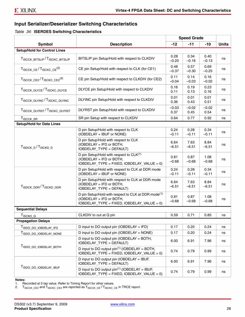
Input Serializer/Deserializer Switching Characteristics
Table 34: ISERDES Switching Characteristics
Symbol Description
Speed Grade
Units-12 -11 -10
Setup/Hold for Control Lines
TISCCK_BITSLIP / TISCKC_BITSLIP BITSLIP pin Setup/Hold with respect to CLKDIV0.28
–0.200.34–0.16
0.40–0.13
ns
TISCCK_CE / TISCKC_CE(2) CE pin Setup/Hold with respect to CLK (for CE1)
0.48–0.37
0.57–0.30
0.69–0.25
ns
TISCCK_CE2 / TISCKC_CE2(2) CE pin Setup/Hold with respect to CLKDIV (for CE2)
0.11–0.04
0.14–0.03
0.16–0.02
ns
TISCCK_DLYCE / TISCKC_DLYCE DLYCE pin Setup/Hold with respect to CLKDIV0.160.11
0.190.13
0.230.16
ns
TISCCK_DLYINC / TISCKC_DLYINC DLYINC pin Setup/Hold with respect to CLKDIV0.010.36
0.010.43
0.010.51
ns
TISCCK_DLYRST / TISCKC_DLYRST DLYRST pin Setup/Hold with respect to CLKDIV–0.030.37
–0.020.45
–0.020.54
ns
TISCCK_SR SR pin Setup with respect to CLKDIV 0.64 0.77 0.92 ns
Setup/Hold for Data Lines
TISDCK_D / TISCKD_D
D pin Setup/Hold with respect to CLK (IOBDELAY = IBUF or NONE)
0.24–0.11
0.28–0.11
0.34–0.11
ns
D pin Setup/Hold with respect to CLK (IOBDELAY = IFD or BOTH, IOBDELAY_TYPE = DEFAULT)
6.64–6.51
7.63–6.51
8.84–6.51
ns
D pin Setup/Hold with respect to CLK(1) (IOBDELAY = IFD or BOTH, IOBDELAY_TYPE = FIXED, IOBDELAY_VALUE = 0)
0.81–0.68
0.87–0.68
1.08–0.68
ns
TISDCK_DDR / TISCKD_DDR
D pin Setup/Hold with respect to CLK at DDR mode (IOBDELAY = IBUF or NONE)
0.24–0.11
0.28–0.11
0.34–0.11
ns
D pin Setup/Hold with respect to CLK at DDR mode (IOBDELAY = IFD or BOTH, IOBDELAY_TYPE = DEFAULT)
6.64–6.51
7.63–6.51
8.84–6.51
ns
D pin Setup/Hold with respect to CLK at DDR mode(1) (IOBDELAY = IFD or BOTH, IOBDELAY_TYPE = FIXED, IOBDELAY_VALUE = 0)
0.81–0.68
0.87–0.68
1.08–0.68
ns
Sequential Delays
TISCKO_Q CLKDIV to out at Q pin 0.59 0.71 0.85 ns
Propagation Delays
TISDO_DO_IOBDELAY_IFD D input to DO output pin (IOBDELAY = IFD) 0.17 0.20 0.24 ns
TISDO_DO_IOBDELAY_NONE D input to DO output pin (IOBDELAY = NONE) 0.17 0.20 0.24 ns
TISDO_DO_IOBDELAY_BOTH
D input to DO output pin (IOBDELAY = BOTH, IOBDELAY_TYPE = DEFAULT)
6.00 6.91 7.96 ns
D input to DO output pin(1) (IOBDELAY = BOTH, IOBDELAY_TYPE = FIXED, IOBDELAY_VALUE = 0)
0.74 0.79 0.99 ns
TISDO_DO_IOBDELAY_IBUF
D input to DO output pin (IOBDELAY = IBUF, IOBDELAY_TYPE = DEFAULT)
6.00 6.91 7.96 ns
D input to DO output pin(1) (IOBDELAY = IBUF, IOBDELAY_TYPE = FIXED, IOBDELAY_VALUE = 0)
0.74 0.79 0.99 ns
Notes: 1. Recorded at 0 tap value. Refer to Timing Report for other values.2. TISCCK_CE2 and TISCKC_CE2 are reported as TISCCK_CE / TISCKC_CE in TRCE report.

Virtex-4 FPGA Data Sheet: DC and Switching Characteristics
DS302 (v3.7) September 9, 2009 www.xilinx.comProduct Specification 29
Input Delay Switching Characteristics
Table 35: Input Delay Switching Characteristics
Symbol Description
Speed Grade
Units-12 -11 -10
IDELAYCTRL
TIDELAYCTRLCO_RDYReset to Ready for IDELAYCTRL (Maximum)
3.00 3.00 3.00 µs
FIDELAYCTRL_REF REFCLK frequency 200 200 200 MHz
IDELAYCTRL_REF_PRECISION(2) REFCLK precision ±10 ±10 ±10 MHz
TIDELAYCTRL_RPW Minimum Reset pulse width 50.0 50.0 50.0 ns
IDELAY
TIDELAYRESOLUTION IDELAY Chain Delay Resolution 75 75 75 ps
TIDELAYTOTAL_ERR Cumulative delay at a given tap(3) [(tap −1) x 75 +34] ± 0.07[(tap −1) x 75 +34]
ps
TIDELAYPAT_JIT
Pattern dependent period jitter in delay chain for clock pattern
0 0 0 Note (4)
Pattern dependent period jitter in delay chain for random data pattern (PRBS 23)
10 ± 2 10 ± 2 10 ± 2 Note (4)
FMAX C clock maximum frequency 300 250 250 MHz
Notes: 1. Refer to Xilinx Application Note XAPP707 for details on IDELAY timing characteristics.2. See the “REFCLK - Reference Clock” section (specific to IDELAYCTRL) in the Virtex-4 FPGA User Guide: Chapter 7, SelectIO Logic Resources.3. This value accounts for tap 0, an anomaly in the tap chain with an average value of 34 ps.4. Units in ps peak-to-peak per tap.
Virtex-4 FPGA Data Sheet: DC and Switching Characteristics
DS302 (v3.7) September 9, 2009 www.xilinx.comProduct Specification 30
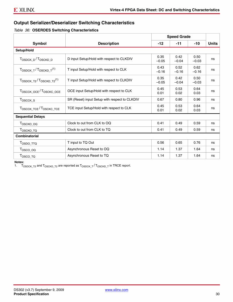
Output Serializer/Deserializer Switching Characteristics
Table 36: OSERDES Switching Characteristics
Symbol Description
Speed Grade
Units-12 -11 -10
Setup/Hold
TOSDCK_D / TOSCKD_D D input Setup/Hold with respect to CLKDIV0.35
–0.050.42
–0.040.50–0.03
ns
TOSDCK_T / TOSCKD_T(1) T input Setup/Hold with respect to CLK
0.43–0.16
0.52–0.16
0.62–0.16
ns
TOSDCK_T2 / TOSCKD_T2(1) T input Setup/Hold with respect to CLKDIV
0.35–0.05
0.42–0.04
0.50–0.03
ns
TOSCCK_OCE / TOSCKC_OCE OCE input Setup/Hold with respect to CLK0.450.01
0.530.02
0.640.03
ns
TOSCCK_S SR (Reset) input Setup with respect to CLKDIV 0.67 0.80 0.96 ns
TOSCCK_TCE / TOSCKC_TCE TCE input Setup/Hold with respect to CLK0.450.01
0.530.02
0.640.03
ns
Sequential Delays
TOSCKO_OQ Clock to out from CLK to OQ 0.41 0.49 0.59 ns
TOSCKO_TQ Clock to out from CLK to TQ 0.41 0.49 0.59 ns
Combinatorial
TOSDO_TTQ T input to TQ Out 0.56 0.65 0.76 ns
TOSCO_OQ Asynchronous Reset to OQ 1.14 1.37 1.64 ns
TOSCO_TQ Asynchronous Reset to TQ 1.14 1.37 1.64 ns
Notes: 1. TOSDCK_T2 and TOSCKD_T2 are reported as TOSDCK_T / TOSCKD_T in TRCE report.

Virtex-4 FPGA Data Sheet: DC and Switching Characteristics
DS302 (v3.7) September 9, 2009 www.xilinx.comProduct Specification 31
CLB Switching Characteristics
Table 37: CLB Switching Characteristics
Symbol Description
Speed Grade
Units
-12 -11 -10
XC4VFX(2) XC4VLX/SX ALL DEVICES
Combinatorial Delays
TILO 4-input function: F/G inputs to X/Y outputs 0.15 0.15 0.17 0.20 ns, Max
TIF5 5-input function: F/G inputs to F5 output 0.36 0.35 0.40 0.46 ns, Max
TIF5X 5-input function: F/G inputs to X output 0.44 0.43 0.49 0.57 ns, Max
TIF6Y FXINA or FXINB inputs to YMUX output 0.30 0.30 0.34 0.39 ns, Max
TINAFX FXINA input to FX output via MUXFX 0.21 0.21 0.23 0.27 ns, Max
TINBFX FXINB input to FX output via MUXFX 0.21 0.20 0.23 0.26 ns, Max
TBXX BX input to XMUX output 0.59 0.58 0.65 0.76 ns, Max
TBYY BY input to YMUX output 0.43 0.43 0.48 0.56 ns, Max
TBXCY BX input to COUT output – Getting into carry chain(3) 0.60 0.59 0.66 0.78 ns, Max
TBYCY BY input to COUT output – Getting into carry chain(3) 0.49 0.48 0.54 0.63 ns, Max
TBYP CIN input to COUT output – Carry chain delay(3) 0.07 0.07 0.08 0.09 ns, Max
TOPCYF F input to COUT output – Getting out from carry chain(3) 0.45 0.44 0.50 0.58 ns, Max
TOPCYG G input to COUT output – Getting out from carry chain(3) 0.44 0.43 0.48 0.57 ns, Max
Sequential Delays
TCKO FF Clock CLK to XQ/YQ outputs 0.28 0.28 0.31 0.36 ns, Max
TCKLO Latch Clock CLK to XQ/YQ outputs 0.37 0.36 0.41 0.48 ns, Max
Setup and Hold Times of CLB Flip-Flops Before/After Clock CLK
TDICK / TCKDI BX/BY inputs0.36–0.09
0.36–0.09
0.40–0.09
0.47–0.09
ns, Min
TCECK / TCKCE CE input0.58–0.16
0.57–0.16
0.64–0.16
0.75–0.16
ns, Min
TFXCK / TCKFX FXINA/FXINB inputs0.42–0.14
0.41–0.14
0.46–0.14
0.54–0.14
ns, Min
TSRCK / TCKSR SR/BY inputs (synchronous)1.04–0.74
1.02–0.73
1.15–0.73
1.35–0.73
ns, Min
TCINCK / TCKCIN CIN Data Inputs (DI) – Getting out from carry chain(3) 0.52–0.23
0.51–0.23
0.57–0.23
0.67–0.23
ns, Min
Set/Reset
TRPW Minimum Pulse Width, SR/BY inputs 0.54 0.53 0.59 0.70 ns, Min
TRQ Delay from SR/BY inputs to XQ/YQ outputs (asynchronous)
1.05 1.03 1.15 1.35 ns, Max
FTOG Toggle Frequency (MHz) (for export control) 1181 1205 1205(4) 1028 MHz
Notes: 1. A Zero “0” Hold Time listing indicates no hold time or a negative hold time. Negative values cannot be guaranteed “best-case,” but if a “0” is listed,
there is no positive hold time.2. The values in this column apply to all XC4VFX -12 parts except XC4VFX12 -12. For XC4VFX12 -12 values, use the values in the adjacent 4VLX/SX
-12 column.3. These items are of interest for Carry Chain applications.4. XC4VFX -11 devices are 1181 MHz.
Virtex-4 FPGA Data Sheet: DC and Switching Characteristics
DS302 (v3.7) September 9, 2009 www.xilinx.comProduct Specification 32
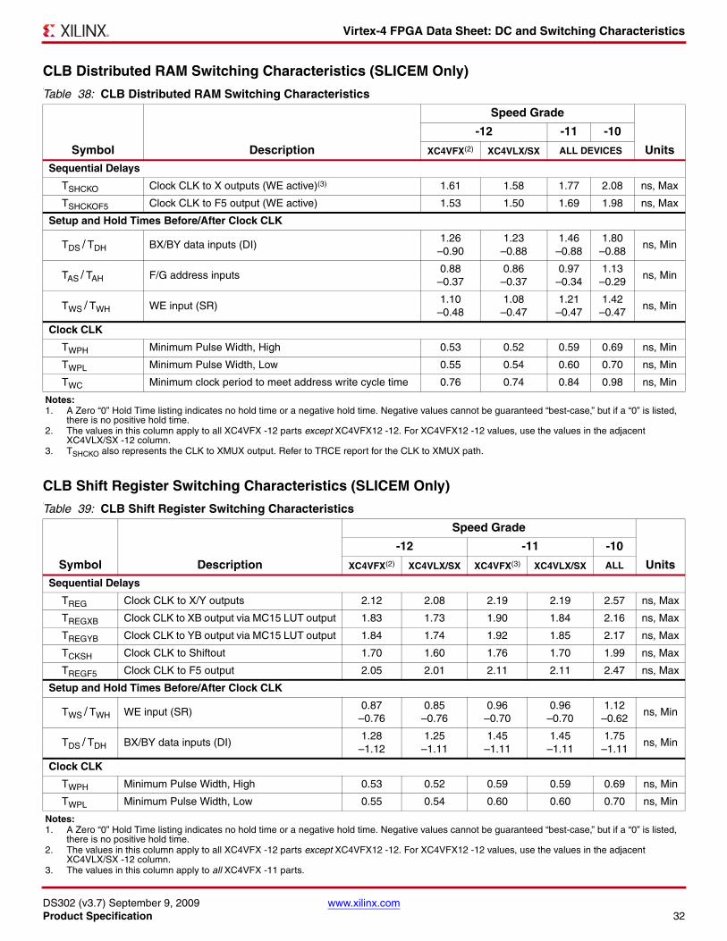
CLB Distributed RAM Switching Characteristics (SLICEM Only))
CLB Shift Register Switching Characteristics (SLICEM Only))
Table 38: CLB Distributed RAM Switching Characteristics
Symbol Description
Speed Grade
Units
-12 -11 -10
XC4VFX(2) XC4VLX/SX ALL DEVICES
Sequential Delays
TSHCKO Clock CLK to X outputs (WE active)(3) 1.61 1.58 1.77 2.08 ns, Max
TSHCKOF5 Clock CLK to F5 output (WE active) 1.53 1.50 1.69 1.98 ns, Max
Setup and Hold Times Before/After Clock CLK
TDS / TDH BX/BY data inputs (DI)1.26
–0.901.23
–0.881.46
–0.881.80–0.88
ns, Min
TAS / TAH F/G address inputs0.88
–0.370.86
–0.370.97
–0.341.13–0.29
ns, Min
TWS / TWH WE input (SR)1.10
–0.481.08
–0.471.21
–0.471.42–0.47
ns, Min
Clock CLK
TWPH Minimum Pulse Width, High 0.53 0.52 0.59 0.69 ns, Min
TWPL Minimum Pulse Width, Low 0.55 0.54 0.60 0.70 ns, Min
TWC Minimum clock period to meet address write cycle time 0.76 0.74 0.84 0.98 ns, Min
Notes: 1. A Zero “0” Hold Time listing indicates no hold time or a negative hold time. Negative values cannot be guaranteed “best-case,” but if a “0” is listed,
there is no positive hold time.2. The values in this column apply to all XC4VFX -12 parts except XC4VFX12 -12. For XC4VFX12 -12 values, use the values in the adjacent
XC4VLX/SX -12 column.3. TSHCKO also represents the CLK to XMUX output. Refer to TRCE report for the CLK to XMUX path.
Table 39: CLB Shift Register Switching Characteristics
Symbol Description
Speed Grade
Units
-12 -11 -10
XC4VFX(2) XC4VLX/SX XC4VFX(3) XC4VLX/SX ALL
Sequential Delays
TREG Clock CLK to X/Y outputs 2.12 2.08 2.19 2.19 2.57 ns, Max
TREGXB Clock CLK to XB output via MC15 LUT output 1.83 1.73 1.90 1.84 2.16 ns, Max
TREGYB Clock CLK to YB output via MC15 LUT output 1.84 1.74 1.92 1.85 2.17 ns, Max
TCKSH Clock CLK to Shiftout 1.70 1.60 1.76 1.70 1.99 ns, Max
TREGF5 Clock CLK to F5 output 2.05 2.01 2.11 2.11 2.47 ns, Max
Setup and Hold Times Before/After Clock CLK
TWS / TWH WE input (SR)0.87–0.76
0.85–0.76
0.96–0.70
0.96–0.70
1.12–0.62
ns, Min
TDS / TDH BX/BY data inputs (DI)1.28–1.12
1.25–1.11
1.45–1.11
1.45–1.11
1.75–1.11
ns, Min
Clock CLK
TWPH Minimum Pulse Width, High 0.53 0.52 0.59 0.59 0.69 ns, Min
TWPL Minimum Pulse Width, Low 0.55 0.54 0.60 0.60 0.70 ns, Min
Notes: 1. A Zero “0” Hold Time listing indicates no hold time or a negative hold time. Negative values cannot be guaranteed “best-case,” but if a “0” is listed,
there is no positive hold time.2. The values in this column apply to all XC4VFX -12 parts except XC4VFX12 -12. For XC4VFX12 -12 values, use the values in the adjacent
XC4VLX/SX -12 column.3. The values in this column apply to all XC4VFX -11 parts.

Virtex-4 FPGA Data Sheet: DC and Switching Characteristics
DS302 (v3.7) September 9, 2009 www.xilinx.comProduct Specification 33
Block RAM and FIFO Switching Characteristics
Table 40: Block RAM Switching Characteristics
Symbol Description
Speed Grade
Units-12 -11 -10
Sequential Delays
TRCKO_DORA
Clock CLK to DOUT output (without output register)(2) 1.65 1.83 2.10 ns, Max
Clock CLK to DOUT output with ECC(without output register)
3.00 3.33 3.83 ns, Max
TRCKO_DOA
Clock CLK to DOUT output (with output register)(3) 0.72 0.80 0.92 ns, Max
Clock CLK to DOUT output with ECC (with output register)
2.00 2.20 2.50 ns, Max
Setup and Hold Times Before Clock CLK
TRCCK_ADDR / TRCKC_ADDR ADDR inputs0.340.26
0.370.28
0.430.33
ns, Min
TRDCK_DI / TRCKD_DI DIN inputs(4) 0.180.26
0.200.28
0.230.33
ns, Min
TRCCK_EN / TRCKC_EN EN input(5) 0.410.26
0.450.28
0.520.33
ns, Min
TRCCK_REGCE /TRCKC_REGCE CE input of output register0.250.26
0.270.28
0.320.33
ns, Min
TRCCK_SSR / TRCKC_SSR RST input0.250.26
0.270.28
0.320.33
ns, Min
TRCCK_WE / TRCKC_WE WEN input0.590.26
0.650.28
0.750.33
ns, Min
Maximum Frequency
FMAX Write first and no change mode 500.00 450.45 400.00 MHz
FMAX Read first mode 500.00 450.45 400.00 MHz
CLK-to-CLK Read first mode 500.00 450.45 400.00 MHz
Notes: 1. A Zero “0” Hold Time listing indicates no hold time or a negative hold time. Negative values cannot be guaranteed “best-case,” but if a “0” is listed,
there is no positive hold time.2. TRCKO_DORA includes TRCKO_DOWA, TRCKO_DOPAR, and TRCKO_DOPAW as well as the B port equivalent timing parameters.3. TRCKO_DOA includes TRCKO_DOPA as well as the B port equivalent timing parameters.4. TRCKO_DI includes both A and B inputs as well as the parity inputs of A and B.5. Xilinx block RAMs do not have asynchronous inputs on an enabled port address. During the time that a port is enabled, its addresses must be stable
during the specified set-up time. Do not create an asynchronous input on an enabled port address.

Virtex-4 FPGA Data Sheet: DC and Switching Characteristics
DS302 (v3.7) September 9, 2009 www.xilinx.comProduct Specification 34
Table 41: FIFO Switching Characteristics
Symbol Description
Speed Grade
Units-12 -11 -10
Sequential Delays
TFCKO_DO Clock CLK to DO output(2) 0.72 0.80 0.92 ns, Max
TFCKO_FLAGS Clock CLK to FIFO flags outputs(3) 0.93 1.04 1.19 ns, Max
TFCKO_POINTERS Clock CLK to FIFO pointer outputs(4) 1.16 1.29 1.48 ns, Max
Setup and Hold Times Before Clock CLK
TFDCK_DI / TFCKD_DI DI input(5) 0.180.26
0.200.28
0.230.33
ns, Min
TFCCK_EN / TFCKC_EN Enable inputs(6) 0.660.26
0.730.28
0.840.33
ns, Min
Reset Delays
TFCO_FLAGS Reset RST to FLAGS(7) 1.32 1.46 1.68 ns, Max
Maximum Frequency
FMAX FIFO in all modes 500.00 450.45 400.00 MHz
Notes: 1. A Zero “0” Hold Time listing indicates no hold time or a negative hold time. Negative values cannot be guaranteed “best-case,” but if a “0” is listed,
there is no positive hold time.2. TFCKO_DO includes parity output (TFCKO_DOP).3. TFCKO_FLAGS includes the following parameters: TFCKO_AEMPTY, TFCKO_AFULL, TFCKO_EMPTY, TFCKO_FULL, TFCKO_RDERR, TFCKO_WRERR.4. TFCKO_POINTERS includes both TFCKO_RDCOUNT and TFCKO_WRCOUNT.5. TFDCK_DI includes parity inputs (TFDCK_DIP).6. TFCCK_EN includes both WRITE and READ enable.7. TFCO_FLAGS includes the following flags: AEMPTY, AFULL, EMPTY, FULL, RDERR, WRERR, RDCOUNT and WRCOUNT.
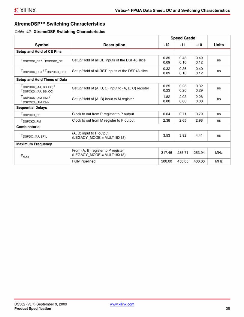
Virtex-4 FPGA Data Sheet: DC and Switching Characteristics
DS302 (v3.7) September 9, 2009 www.xilinx.comProduct Specification 35
XtremeDSP™ Switching Characteristics
Table 42: XtremeDSP Switching Characteristics
Symbol Description
Speed Grade
Units-12 -11 -10
Setup and Hold of CE Pins
TDSPCCK_CE / TDSPCKC_CE Setup/Hold of all CE inputs of the DSP48 slice0.390.09
0.430.10
0.490.12
ns
TDSPCCK_RST / TDSPCKC_RST Setup/Hold of all RST inputs of the DSP48 slice0.320.09
0.360.10
0.400.12
ns
Setup and Hold Times of Data
TDSPDCK_{AA, BB, CC} /TDSPCKD_{AA, BB, CC}
Setup/Hold of {A, B, C} input to {A, B, C} register0.250.23
0.280.26
0.320.29
ns
TDSPDCK_{AM, BM} /TDSPCKD_{AM, BM}
Setup/Hold of {A, B} input to M register1.820.00
2.030.00
2.280.00
ns
Sequential Delays
TDSPCKO_PP Clock to out from P register to P output 0.64 0.71 0.79 ns
TDSPCKO_PM Clock to out from M register to P output 2.38 2.65 2.98 ns
Combinatorial
TDSPDO_{AP, BP}L{A, B} input to P output (LEGACY_MODE = MULT18X18)
3.53 3.92 4.41 ns
Maximum Frequency
FMAX
From {A, B} register to P register (LEGACY_MODE = MULT18X18)
317.46 285.71 253.94 MHz
Fully Pipelined 500.00 450.05 400.00 MHz

Virtex-4 FPGA Data Sheet: DC and Switching Characteristics
DS302 (v3.7) September 9, 2009 www.xilinx.comProduct Specification 36
Configuration Switching Characteristics
Table 43: Configuration Switching Characteristics
Symbol Description
Speed Grade
Units-12 -11 -10
Power-up Timing Characteristics
TCONFIG(1,2) Maximum time to configure device after
VCCINT has been applied.10 10 10 minutes
TPL Program Latency 0.5 0.5 0.5µs/frame,
Max
TPOR Power-on-Reset TPL + 10 TPL + 10 TPL + 10 ms, Max
TICCK CCLK (output) delay 500 500 500 ns, Min
TPROGRAM Program Pulse Width 300 300 300 ns, Min
Master/Slave Serial Mode Programming Switching
TDCC / TCCD DIN Setup/Hold, slave mode0.51.0
0.51.0
0.51.0
ns, Min
TDSCK / TSCKD DIN Setup/Hold, master mode0.51.0
0.51.0
0.51.0
ns, Min
TCCO DOUT 7.5 7.5 7.5 ns, Max
TCCH High Time 2.0 2.0 2.0 ns, Min
TCCL Low Time 2.0 2.0 2.0 ns, Min
FCC_SERIALMaximum Frequency, master mode with respect to nominal CCLK.
100 100 100 MHz, Max
FMAX_SLAVE / FMAX_ICAPMaximum Frequency, slave mode external CCLK
100 100 100 MHz, Max
FMCCTOLFrequency Tolerance, master mode with respect to nominal CCLK.
±50 ±50 ±50 %
SelectMAP Mode Programming Switching
TSMDCC / TSMCCD SelectMAP Data Setup/Hold2.00.0
2.00.0
2.00.0
ns, Min
TSMCSCC / TSMCCCS CS_B Setup/Hold1.00.5
1.00.5
1.00.5
ns, Min
TSMCCW / TSMWCC RDWR_B Setup/Hold6.01.0
6.01.0
6.01.0
ns, Min
TSMCKBY BUSY Propagation Delay 8.0 8.0 8.0 ns, Max
FCC_SELECTMAPMaximum Frequency, master mode with respect to nominal CCLK.
100 100 100 MHz, Max
FMAX_SELECTMAPMaximum Configuration Frequency, slave mode external CCLK
100 100 100 MHz, Max
FMAX_READBACK Maximum Readback Frequency 80 80 80 MHz, Max
FMCCTOLFrequency Tolerance, master mode with respect to nominal CCLK.
±50 ±50 ±50 %
TSMCO SelectMAP Readback Clock-to-Out 8.0 8.0 8.0 ns, Max
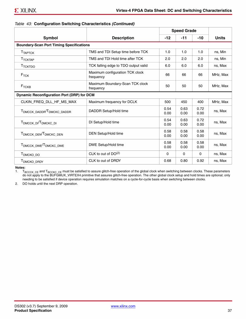
Virtex-4 FPGA Data Sheet: DC and Switching Characteristics
DS302 (v3.7) September 9, 2009 www.xilinx.comProduct Specification 37
Boundary-Scan Port Timing Specifications
TTAPTCK TMS and TDI Setup time before TCK 1.0 1.0 1.0 ns, Min
TTCKTAP TMS and TDI Hold time after TCK 2.0 2.0 2.0 ns, Min
TTCKTDO TCK falling edge to TDO output valid 6.0 6.0 6.0 ns, Max
FTCKMaximum configuration TCK clock frequency
66 66 66 MHz, Max
FTCKBMaximum Boundary-Scan TCK clock frequency
50 50 50 MHz, Max
Dynamic Reconfiguration Port (DRP) for DCM
CLKIN_FREQ_DLL_HF_MS_MAX Maximum frequency for DCLK 500 450 400 MHz, Max
TDMCCK_DADDR/TDMCKC_DADDR DADDR Setup/Hold time0.540.00
0.630.00
0.720.00
ns, Max
TDMCCK_DI/TDMCKC_DI DI Setup/Hold time0.540.00
0.630.00
0.720.00
ns, Max
TDMCCK_DEN/TDMCKC_DEN DEN Setup/Hold time0.580.00
0.580.00
0.580.00
ns, Max
TDMCCK_DWE/TDMCKC_DWE DWE Setup/Hold time0.580.00
0.580.00
0.580.00
ns, Max
TDMCKO_DO CLK to out of DO(2) 0 0 0 ns, Max
TDMCKO_DRDY CLK to out of DRDY 0.68 0.80 0.92 ns, Max
Notes: 1. TBCCCK_CE and TBCCKC_CE must be satisfied to assure glitch-free operation of the global clock when switching between clocks. These parameters
do not apply to the BUFGMUX_VIRTEX4 primitive that assures glitch-free operation. The other global clock setup and hold times are optional; only needing to be satisfied if device operation requires simulation matches on a cycle-for-cycle basis when switching between clocks.
2. DO holds until the next DRP operation.
Table 43: Configuration Switching Characteristics (Continued)
Symbol Description
Speed Grade
Units-12 -11 -10
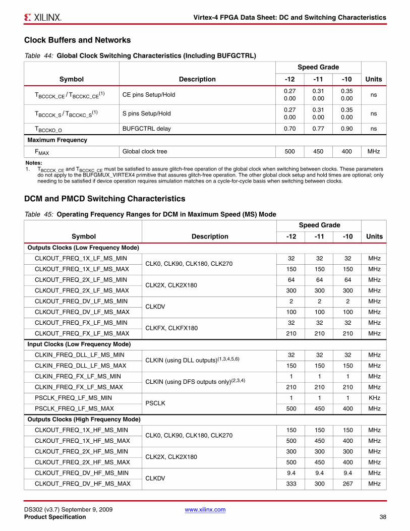
Virtex-4 FPGA Data Sheet: DC and Switching Characteristics
DS302 (v3.7) September 9, 2009 www.xilinx.comProduct Specification 38
Clock Buffers and Networks
DCM and PMCD Switching Characteristics
Table 44: Global Clock Switching Characteristics (Including BUFGCTRL)
Symbol Description
Speed Grade
Units-12 -11 -10
TBCCCK_CE / TBCCKC_CE(1) CE pins Setup/Hold
0.270.00
0.310.00
0.350.00
ns
TBCCCK_S / TBCCKC_S(1) S pins Setup/Hold
0.270.00
0.310.00
0.350.00
ns
TBCCKO_O BUFGCTRL delay 0.70 0.77 0.90 ns
Maximum Frequency
FMAX Global clock tree 500 450 400 MHz
Notes: 1. TBCCCK_CE and TBCCKC_CE must be satisfied to assure glitch-free operation of the global clock when switching between clocks. These parameters
do not apply to the BUFGMUX_VIRTEX4 primitive that assures glitch-free operation. The other global clock setup and hold times are optional; only needing to be satisfied if device operation requires simulation matches on a cycle-for-cycle basis when switching between clocks.
Table 45: Operating Frequency Ranges for DCM in Maximum Speed (MS) Mode
Symbol Description
Speed Grade
Units-12 -11 -10
Outputs Clocks (Low Frequency Mode)
CLKOUT_FREQ_1X_LF_MS_MINCLK0, CLK90, CLK180, CLK270
32 32 32 MHz
CLKOUT_FREQ_1X_LF_MS_MAX 150 150 150 MHz
CLKOUT_FREQ_2X_LF_MS_MINCLK2X, CLK2X180
64 64 64 MHz
CLKOUT_FREQ_2X_LF_MS_MAX 300 300 300 MHz
CLKOUT_FREQ_DV_LF_MS_MINCLKDV
2 2 2 MHz
CLKOUT_FREQ_DV_LF_MS_MAX 100 100 100 MHz
CLKOUT_FREQ_FX_LF_MS_MINCLKFX, CLKFX180
32 32 32 MHz
CLKOUT_FREQ_FX_LF_MS_MAX 210 210 210 MHz
Input Clocks (Low Frequency Mode)
CLKIN_FREQ_DLL_LF_MS_MINCLKIN (using DLL outputs)(1,3,4,5,6)
32 32 32 MHz
CLKIN_FREQ_DLL_LF_MS_MAX 150 150 150 MHz
CLKIN_FREQ_FX_LF_MS_MINCLKIN (using DFS outputs only)(2,3,4)
1 1 1 MHz
CLKIN_FREQ_FX_LF_MS_MAX 210 210 210 MHz
PSCLK_FREQ_LF_MS_MINPSCLK
1 1 1 KHz
PSCLK_FREQ_LF_MS_MAX 500 450 400 MHz
Outputs Clocks (High Frequency Mode)
CLKOUT_FREQ_1X_HF_MS_MINCLK0, CLK90, CLK180, CLK270
150 150 150 MHz
CLKOUT_FREQ_1X_HF_MS_MAX 500 450 400 MHz
CLKOUT_FREQ_2X_HF_MS_MINCLK2X, CLK2X180
300 300 300 MHz
CLKOUT_FREQ_2X_HF_MS_MAX 500 450 400 MHz
CLKOUT_FREQ_DV_HF_MS_MINCLKDV
9.4 9.4 9.4 MHz
CLKOUT_FREQ_DV_HF_MS_MAX 333 300 267 MHz
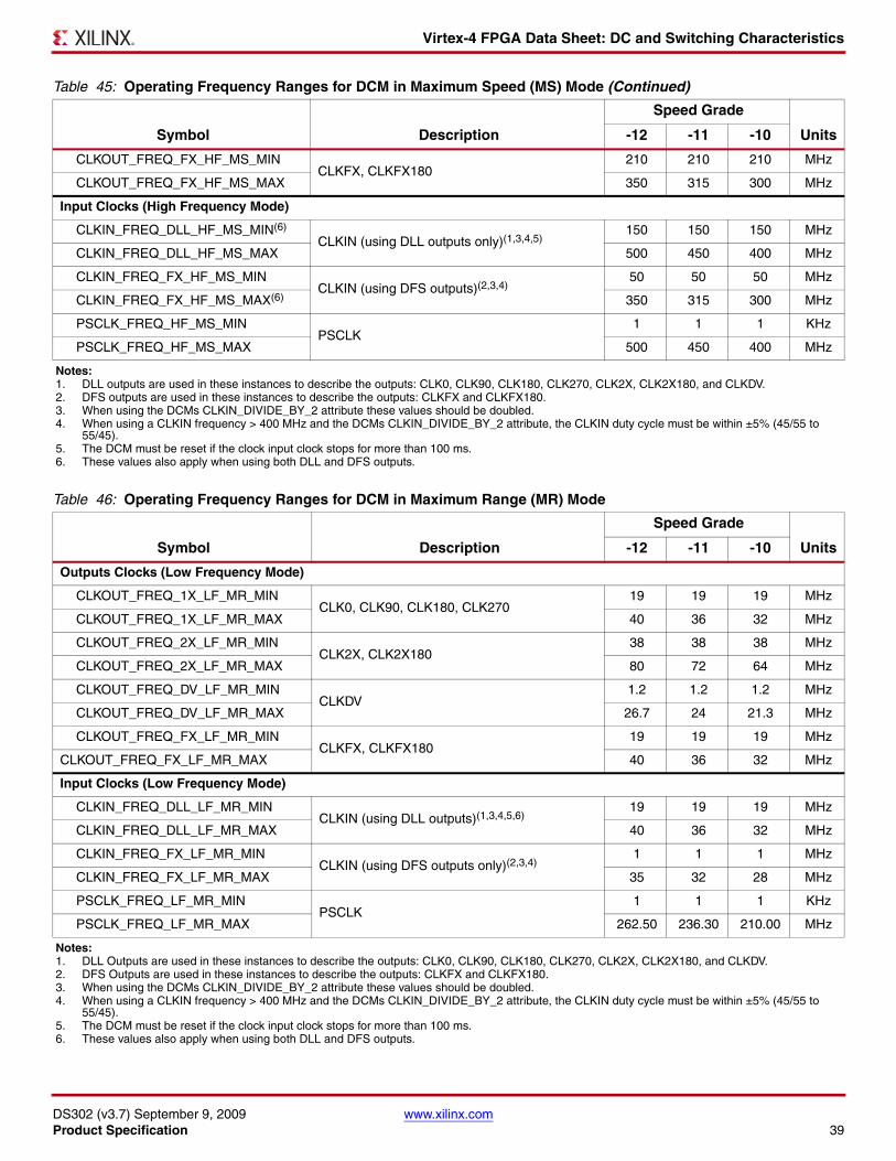
Virtex-4 FPGA Data Sheet: DC and Switching Characteristics
DS302 (v3.7) September 9, 2009 www.xilinx.comProduct Specification 39
CLKOUT_FREQ_FX_HF_MS_MINCLKFX, CLKFX180
210 210 210 MHz
CLKOUT_FREQ_FX_HF_MS_MAX 350 315 300 MHz
Input Clocks (High Frequency Mode)
CLKIN_FREQ_DLL_HF_MS_MIN(6)
CLKIN (using DLL outputs only)(1,3,4,5)150 150 150 MHz
CLKIN_FREQ_DLL_HF_MS_MAX 500 450 400 MHz
CLKIN_FREQ_FX_HF_MS_MINCLKIN (using DFS outputs)(2,3,4)
50 50 50 MHz
CLKIN_FREQ_FX_HF_MS_MAX(6) 350 315 300 MHz
PSCLK_FREQ_HF_MS_MINPSCLK
1 1 1 KHz
PSCLK_FREQ_HF_MS_MAX 500 450 400 MHz
Notes: 1. DLL outputs are used in these instances to describe the outputs: CLK0, CLK90, CLK180, CLK270, CLK2X, CLK2X180, and CLKDV. 2. DFS outputs are used in these instances to describe the outputs: CLKFX and CLKFX180.3. When using the DCMs CLKIN_DIVIDE_BY_2 attribute these values should be doubled.4. When using a CLKIN frequency > 400 MHz and the DCMs CLKIN_DIVIDE_BY_2 attribute, the CLKIN duty cycle must be within ±5% (45/55 to
55/45).5. The DCM must be reset if the clock input clock stops for more than 100 ms.6. These values also apply when using both DLL and DFS outputs.
Table 45: Operating Frequency Ranges for DCM in Maximum Speed (MS) Mode (Continued)
Symbol Description
Speed Grade
Units-12 -11 -10
Table 46: Operating Frequency Ranges for DCM in Maximum Range (MR) Mode
Symbol Description
Speed Grade
Units-12 -11 -10
Outputs Clocks (Low Frequency Mode)
CLKOUT_FREQ_1X_LF_MR_MINCLK0, CLK90, CLK180, CLK270
19 19 19 MHz
CLKOUT_FREQ_1X_LF_MR_MAX 40 36 32 MHz
CLKOUT_FREQ_2X_LF_MR_MINCLK2X, CLK2X180
38 38 38 MHz
CLKOUT_FREQ_2X_LF_MR_MAX 80 72 64 MHz
CLKOUT_FREQ_DV_LF_MR_MINCLKDV
1.2 1.2 1.2 MHz
CLKOUT_FREQ_DV_LF_MR_MAX 26.7 24 21.3 MHz
CLKOUT_FREQ_FX_LF_MR_MINCLKFX, CLKFX180
19 19 19 MHz
CLKOUT_FREQ_FX_LF_MR_MAX 40 36 32 MHz
Input Clocks (Low Frequency Mode)
CLKIN_FREQ_DLL_LF_MR_MINCLKIN (using DLL outputs)(1,3,4,5,6)
19 19 19 MHz
CLKIN_FREQ_DLL_LF_MR_MAX 40 36 32 MHz
CLKIN_FREQ_FX_LF_MR_MINCLKIN (using DFS outputs only)(2,3,4)
1 1 1 MHz
CLKIN_FREQ_FX_LF_MR_MAX 35 32 28 MHz
PSCLK_FREQ_LF_MR_MINPSCLK
1 1 1 KHz
PSCLK_FREQ_LF_MR_MAX 262.50 236.30 210.00 MHz
Notes: 1. DLL Outputs are used in these instances to describe the outputs: CLK0, CLK90, CLK180, CLK270, CLK2X, CLK2X180, and CLKDV. 2. DFS Outputs are used in these instances to describe the outputs: CLKFX and CLKFX180.3. When using the DCMs CLKIN_DIVIDE_BY_2 attribute these values should be doubled.4. When using a CLKIN frequency > 400 MHz and the DCMs CLKIN_DIVIDE_BY_2 attribute, the CLKIN duty cycle must be within ±5% (45/55 to
55/45).5. The DCM must be reset if the clock input clock stops for more than 100 ms.6. These values also apply when using both DLL and DFS outputs.

Virtex-4 FPGA Data Sheet: DC and Switching Characteristics
DS302 (v3.7) September 9, 2009 www.xilinx.comProduct Specification 40
Table 47: Input Clock Tolerances
Symbol DescriptionFrequency
Range Value Units
Duty Cycle Input Tolerance (in %)
CLKIN_PSCLK_PULSE_RANGE_1 PSCLK only < 1 MHz 25 - 75 %
CLKIN_PSCLK_PULSE_RANGE_1_50
PSCLK and CLKIN
1 – 50 MHz(1) 25 - 75 %
CLKIN_PSCLK_PULSE_RANGE_50_100 50 – 100 MHz(1) 30 - 70 %
CLKIN_PSCLK_PULSE_RANGE_100_200 100 – 200 MHz(1) 40 - 60 %
CLKIN_PSCLK_PULSE_RANGE_200_400 200 – 400 MHz(1) 45 - 55 %
CLKIN_PSCLK_PULSE_RANGE_400 > 400 MHz 45 - 55 %
Speed Grade
-12 -11 -10
Input Clock Cycle-Cycle Jitter (Low Frequency Mode)
CLKIN_CYC_JITT_DLL_LF CLKIN (using DLL outputs)(2,5,6) ±300 ±300 ±345 ps
CLKIN_CYC_JITT_FX_LF CLKIN (using DFS outputs)(3) ±300 ±300 ±345 ps
Input Clock Cycle-Cycle Jitter (High Frequency Mode)
CLKIN_CYC_JITT_DLL_HF CLKIN (using DLL outputs)(2,5,6) ±150 ±150 ±173 ps
CLKIN_CYC_JITT_FX_HF CLKIN (using DFS outputs)(3) ±150 ±150 ±173 ps
Input Clock Period Jitter (Low Frequency Mode)
CLKIN_PER_JITT_DLL_LF CLKIN (using DLL outputs)(2,5,6) ±1.0 ±1.0 ±1.15 ns
CLKIN_PER_JITT_FX_LF CLKIN (using DFS outputs)(3) ±1.0 ±1.0 ±1.15 ns
Input Clock Period Jitter (High Frequency Mode)
CLKIN_PER_JITT_DLL_HF CLKIN (using DLL outputs)(2,5,6) ±1.0 ±1.0 ±1.15 ns
CLKIN_PER_JITT_FX_HF CLKIN (using DFS outputs)(3) ±1.0 ±1.0 ±1.15 ns
Feedback Clock Path Delay Variation
CLKFB_DELAY_VAR_EXT CLKFB off-chip feedback ±1.0 ±1.0 ±1.15 ns
Notes: 1. For boundary frequencies, use the more restrictive specifications.2. DLL Outputs are used in these instances to describe the outputs: CLK0, CLK90, CLK180, CLK270, CLK2X, CLK2X180, and CLKDV.3. DFS Outputs are used in these instances to describe the outputs: CLKFX and CLKFX180.4. If both DLL and DFS outputs are used, follow the more restrictive specifications.5. The DCM must be reset if the clock input clock stops for more than 100 ms.6. These values also apply when using both DLL and DFS outputs.

Virtex-4 FPGA Data Sheet: DC and Switching Characteristics
DS302 (v3.7) September 9, 2009 www.xilinx.comProduct Specification 41
Output Clock Jitter
Output Clock Phase Alignment
Table 48: Output Clock Jitter
Description Symbol Constraints
Speed Grade
Units-12 -11 -10
Clock Synthesis Period Jitter
CLK0 CLKOUT_PER_JITT_0 ±100 ±100 ±100 ps
CLK90 CLKOUT_PER_JITT_90 ±150 ±150 ±150 ps
CLK180 CLKOUT_PER_JITT_180 ±150 ±150 ±150 ps
CLK270 CLKOUT_PER_JITT_270 ±150 ±150 ±150 ps
CLK2X, CLK2X180 CLKOUT_PER_JITT_2X ±200 ±200 ±200 ps
CLKDV (integer division) CLKOUT_PER_JITT_DV1 ±150 ±150 ±150 ps
CLKDV (non-integer division) CLKOUT_PER_JITT_DV2 ±300 ±300 ±300 ps
CLKFX, CLKFX180 CLKOUT_PER_JITT_FX Note (2) Note (2) Note (2) ps
Notes: 1. PMCD outputs are not included in this table because they do not introduce jitter.2. Values for this parameter are available from the architecture wizard.
Table 49: Output Clock Phase Alignment
Description Symbol Constraints
Speed Grade
Units-12 -11 -10
Phase Offset Between CLKIN and CLKFB
CLKIN / CLKFB CLKIN_CLKFB_PHASE ±120 ±120 ±120 ps
Phase Offset Between Any DCM Outputs
All CLK outputs CLKOUT_PHASE ±140 ±140 ±140 ps
Duty Cycle Precision
DLL outputs(1) CLKOUT_DUTY_CYCLE_DLL(3,4) ±150 ±150 ±150 ps
DFS outputs(2) CLKOUT_DUTY_CYCLE_FX(4) ±200 ±200 ±200 ps
Notes: 1. DLL Outputs are used in these instances to describe the outputs: CLK0, CLK90, CLK180, CLK270, CLK2X, CLK2X180, and CLKDV.2. DFS Outputs are used in these instances to describe the outputs: CLKFX and CLKFX180.3. CLKOUT_DUTY_CYCLE_DLL applies to the 1X clock outputs (CLK0, CLK90, CLK180, and CLK270) only if DUTY_CYCLE_CORRECTION=TRUE.4. The measured value includes the duty cycle distortion of the global clock tree.

Virtex-4 FPGA Data Sheet: DC and Switching Characteristics
DS302 (v3.7) September 9, 2009 www.xilinx.comProduct Specification 42
Table 50: Miscellaneous Timing Parameters
Symbol Description
Speed Grade
Units-12 -11 -10
Time Required to Achieve LOCK
T_LOCK_DLL_240 DLL output – Frequency range > 240 MHz (2) 20 20 20 µs
T_LOCK_DLL_120_240 DLL output – Frequency range 120 - 240 MHz (1,2) 63 63 63 µs
T_LOCK_DLL_60_120 DLL output – Frequency range 60 - 120 MHz (1,2) 225 225 225 µs
T_LOCK_DLL_50_60 DLL output – Frequency range 50 - 60 MHz(1,2) 325 325 325 µs
T_LOCK_DLL_40_50 DLL output – Frequency range 40 - 50 MHz (1,2) 500 500 500 µs
T_LOCK_DLL_30_40 DLL output – Frequency range 30 - 40 MHz (1,2) 900 900 900 µs
T_LOCK_DLL_24_30 DLL output – Frequency range 24 - 30 MHz(1,2) 1250 1250 1250 µs
T_LOCK_DLL_30 DLL output – Frequency range < 30 MHz (2) 1250 1250 1250 µs
T_LOCK_FX_MAX DFS outputs(3) 10 10 10 ms
T_LOCK_DLL_FINE_SHIFT Multiplication factor for DLL lock time with Fine Shift 2 2 2
Fine Phase Shifting
FINE_SHIFT_RANGE_MS Absolute shifting range in maximum speed mode 7 7 7 ns
FINE_SHIFT_RANGE_MR Absolute shifting range in maximum range mode 10 10 10 ns
Delay Lines
DCM_TAP_MS_MIN Tap delay resolution (Min) in maximum speed mode 5 5 5 ps
DCM_TAP_MS_MAX Tap delay resolution (Max) in maximum speed mode 40 40 40 ps
DCM_TAP_MR_MIN Tap delay resolution (Min) in maximum range mode 10 10 10 ps
DCM_TAP_MR_MAX Tap delay resolution (Max) in maximum range mode 60 60 60 ps
Input Signal Requirements
DCM_RESET(4)Minimum duration that RST must be held asserted 200 200 200 ms
Maximum duration that RST can be held asserted(5) 10 10 10 sec
DCM_INPUT_CLOCK_STOPMaximum duration that CLKIN and CLKFB can be stopped(6,7) 100 100 100 ms
Notes: 1. For boundary frequencies, choose the higher delay.2. DLL Outputs are used in these instances to describe the outputs: CLK0, CLK90, CLK180, CLK270, CLK2X, CLK2X180, and CLKDV.3. DFS Outputs are used in these instances to describe the outputs: CLKFX and CLKFX180.4. CLKIN must be present and stable during the DCM_RESET.5. This only applies to production step 1 LX and SX devices. For these devices, use the design solutions described in Answer Record 21127 for support
of longer reset durations. Production step 2 LX and SX devices and all production FX devices do not have this requirement.6. For production step 1 LX and SX devices, use the design solutions described in Answer Record 21127 for support of longer durations of stopped
clocks. For production step 2 LX and SX devices and all production FX devices, the ISE software automatically inserts a small macro to support longer durations of stopped clocks.
7. For all stepping levels, once the input clock is toggling again and stable after being stopped, DCM must be reset.
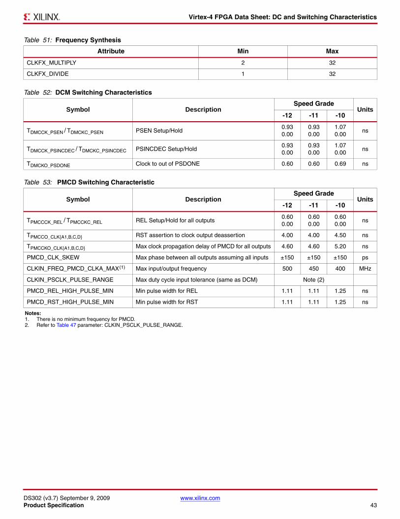
Virtex-4 FPGA Data Sheet: DC and Switching Characteristics
DS302 (v3.7) September 9, 2009 www.xilinx.comProduct Specification 43
Table 51: Frequency Synthesis
Attribute Min Max
CLKFX_MULTIPLY 2 32
CLKFX_DIVIDE 1 32
Table 52: DCM Switching Characteristics
Symbol DescriptionSpeed Grade
Units-12 -11 -10
TDMCCK_PSEN / TDMCKC_PSEN PSEN Setup/Hold0.930.00
0.930.00
1.070.00
ns
TDMCCK_PSINCDEC / TDMCKC_PSINCDEC PSINCDEC Setup/Hold0.930.00
0.930.00
1.070.00
ns
TDMCKO_PSDONE Clock to out of PSDONE 0.60 0.60 0.69 ns
Table 53: PMCD Switching Characteristic
Symbol DescriptionSpeed Grade
Units-12 -11 -10
TPMCCCK_REL / TPMCCKC_REL REL Setup/Hold for all outputs0.600.00
0.600.00
0.600.00
ns
TPMCCO_CLK{A1,B,C,D} RST assertion to clock output deassertion 4.00 4.00 4.50 ns
TPMCCKO_CLK{A1,B,C,D} Max clock propagation delay of PMCD for all outputs 4.60 4.60 5.20 ns
PMCD_CLK_SKEW Max phase between all outputs assuming all inputs ±150 ±150 ±150 ps
CLKIN_FREQ_PMCD_CLKA_MAX(1) Max input/output frequency 500 450 400 MHz
CLKIN_PSCLK_PULSE_RANGE Max duty cycle input tolerance (same as DCM) Note (2)
PMCD_REL_HIGH_PULSE_MIN Min pulse width for REL 1.11 1.11 1.25 ns
PMCD_RST_HIGH_PULSE_MIN Min pulse width for RST 1.11 1.11 1.25 ns
Notes: 1. There is no minimum frequency for PMCD.2. Refer to Table 47 parameter: CLKIN_PSCLK_PULSE_RANGE.

Virtex-4 FPGA Data Sheet: DC and Switching Characteristics
DS302 (v3.7) September 9, 2009 www.xilinx.comProduct Specification 44
System-Synchronous Switching Characteristics
Virtex-4 FPGA Pin-to-Pin Output Parameter Guidelines
All devices are 100% functionally tested. The representative values for typical pin locations and normal clock loading arelisted in Table 54. Values are expressed in nanoseconds unless otherwise noted.
Table 54: Global Clock Input to Output Delay for LVCMOS25 Standard, 12 mA, Fast Slew Rate, with DCM
Symbol Description DeviceSpeed Grade
Units-12 -11 -10
LVCMOS25 Global Clock Input to Output Delay using Output Flip-Flop, 12mA, Fast Slew Rate, with DCM.
TICKOFDCM Global Clock and OFF with DCM XC4VLX15 2.43 2.81 3.25 ns
XC4VLX25 2.60 2.95 3.36 ns
XC4VLX40 2.54 2.91 3.32 ns
XC4VLX60 2.69 3.05 3.45 ns
XC4VLX80 2.88 3.27 3.72 ns
XC4VLX100 2.94 3.33 3.79 ns
XC4VLX160 2.94 3.35 3.82 ns
XC4VLX200 N/A 3.51 4.02 ns
XC4VSX25 2.65 2.99 3.39 ns
XC4VSX35 2.81 3.18 3.60 ns
XC4VSX55 2.83 3.20 3.62 ns
XC4VFX12 2.43 2.78 3.18 ns
XC4VFX20 2.54 2.88 3.26 ns
XC4VFX40 2.87 3.25 3.67 ns
XC4VFX60 2.92 3.31 3.77 ns
XC4VFX100 3.16 3.58 4.06 ns
XC4VFX140 N/A 3.79 4.30 ns
Notes: 1. Listed above are representative values where one global clock input drives one vertical clock line in each accessible column, and where all
accessible IOB and CLB flip-flops are clocked by the global clock net.2. DCM output jitter is already included in the timing calculation.

Virtex-4 FPGA Data Sheet: DC and Switching Characteristics
DS302 (v3.7) September 9, 2009 www.xilinx.comProduct Specification 45
Table 55: Global Clock Input to Output Delay for LVCMOS25 Standard, 12 mA, Fast Slew Rate, without DCM
Symbol Description DeviceSpeed Grade
Units-12 -11 -10
LVCMOS25 Global Clock Input to Output Delay using Output Flip-Flop, 12 mA, Fast Slew Rate, without DCM.
TICKOF Global Clock and OFF without DCM XC4VLX15 6.42 7.22 8.14 ns
XC4VLX25 6.50 7.32 8.25 ns
XC4VLX40 6.70 7.54 8.50 ns
XC4VLX60 6.86 7.72 8.70 ns
XC4VLX80 6.98 7.85 8.85 ns
XC4VLX100 7.23 8.15 9.18 ns
XC4VLX160 7.46 8.40 9.46 ns
XC4VLX200 N/A 8.79 9.88 ns
XC4VSX25 6.69 7.52 8.47 ns
XC4VSX35 6.75 7.59 8.56 ns
XC4VSX55 7.10 7.99 9.00 ns
XC4VFX12 6.41 7.21 8.13 ns
XC4VFX20 6.60 7.42 8.37 ns
XC4VFX40 6.97 7.84 8.83 ns
XC4VFX60 6.98 7.86 8.85 ns
XC4VFX100 7.46 8.40 9.45 ns
XC4VFX140 N/A 8.80 9.90 ns
Notes: 1. Listed above are representative values where one global clock input drives one vertical clock line in each accessible column, and where all
accessible IOB and CLB flip-flops are clocked by the global clock net.
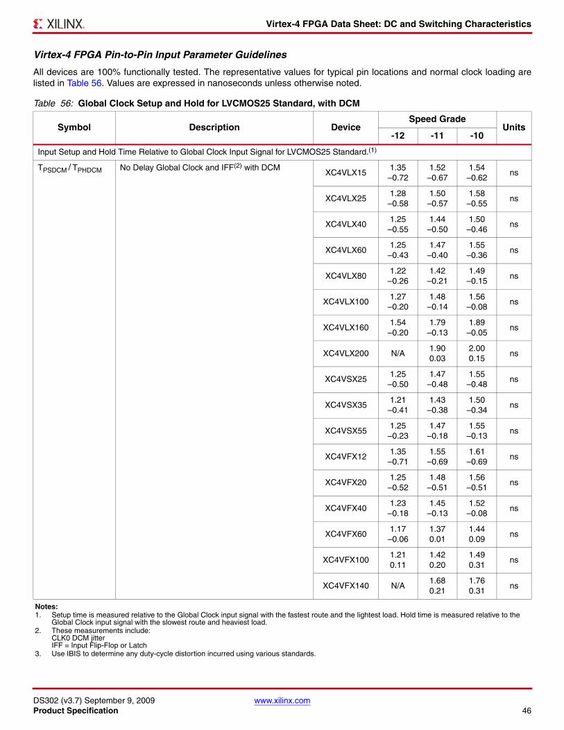
Virtex-4 FPGA Data Sheet: DC and Switching Characteristics
DS302 (v3.7) September 9, 2009 www.xilinx.comProduct Specification 46
Virtex-4 FPGA Pin-to-Pin Input Parameter Guidelines
All devices are 100% functionally tested. The representative values for typical pin locations and normal clock loading arelisted in Table 56. Values are expressed in nanoseconds unless otherwise noted.
Table 56: Global Clock Setup and Hold for LVCMOS25 Standard, with DCM
Symbol Description DeviceSpeed Grade
Units-12 -11 -10
Input Setup and Hold Time Relative to Global Clock Input Signal for LVCMOS25 Standard.(1)
TPSDCM / TPHDCM No Delay Global Clock and IFF(2) with DCMXC4VLX15
1.35–0.72
1.52–0.67
1.54–0.62
ns
XC4VLX251.28–0.58
1.50–0.57
1.58–0.55
ns
XC4VLX401.25–0.55
1.44–0.50
1.50–0.46
ns
XC4VLX601.25–0.43
1.47–0.40
1.55–0.36
ns
XC4VLX801.22–0.26
1.42–0.21
1.49–0.15
ns
XC4VLX1001.27–0.20
1.48–0.14
1.56–0.08
ns
XC4VLX1601.54–0.20
1.79–0.13
1.89–0.05
ns
XC4VLX200 N/A1.900.03
2.000.15
ns
XC4VSX251.25–0.50
1.47–0.48
1.55–0.48
ns
XC4VSX351.21–0.41
1.43–0.38
1.50–0.34
ns
XC4VSX551.25–0.23
1.47–0.18
1.55–0.13
ns
XC4VFX121.35–0.71
1.55–0.69
1.61–0.69
ns
XC4VFX201.25–0.52
1.48–0.51
1.56–0.51
ns
XC4VFX401.23–0.18
1.45–0.13
1.52–0.08
ns
XC4VFX601.17–0.06
1.370.01
1.440.09
ns
XC4VFX1001.210.11
1.420.20
1.490.31
ns
XC4VFX140 N/A1.680.21
1.760.31
ns
Notes: 1. Setup time is measured relative to the Global Clock input signal with the fastest route and the lightest load. Hold time is measured relative to the
Global Clock input signal with the slowest route and heaviest load. 2. These measurements include:
CLK0 DCM jitterIFF = Input Flip-Flop or Latch
3. Use IBIS to determine any duty-cycle distortion incurred using various standards.

Virtex-4 FPGA Data Sheet: DC and Switching Characteristics
DS302 (v3.7) September 9, 2009 www.xilinx.comProduct Specification 47
Table 57: Global Clock Setup and Hold for LVCMOS25 Standard, with DCM in Source-Synchronous Mode
Symbol Description Device
Speed Grade
Units–12 –11 –10
Example Data Input Setup and Hold Times Relative to a Forwarded Clock Input Pin,(1) Using DCM and Global Clock Buffer. For situations where clock and data inputs conform to different standards, adjust the setup and hold values accordingly using the values shown in IOB Switching Characteristics(1,2), page 19.
TPSDCM_0 /TPHDCM_0
No Delay Global Clock and IFF(2) with DCM in Source-Synchronous Mode
XC4VLX15–0.330.73
–0.330.88
–0.331.03
ns
XC4VLX25–0.290.86
–0.290.97
–0.291.09
ns
XC4VLX40–0.370.90
–0.371.04
–0.371.19
ns
XC4VLX60–0.321.02
–0.321.15
–0.321.29
ns
XC4VLX80–0.381.18
–0.381.34
–0.381.50
ns
XC4VLX100–0.311.24
–0.311.41
–0.311.57
ns
XC4VLX160–0.311.50
–0.311.69
–0.311.89
ns
XC4VLX200 N/A–0.311.97
–0.312.19
ns
XC4VSX25–0.320.95
–0.321.07
–0.321.17
ns
XC4VSX35–0.371.04
–0.371.17
–0.371.31
ns
XC4VSX55–0.321.22
–0.321.36
–0.321.52
ns
XC4VFX12–0.260.73
–0.260.86
–0.260.96
ns
XC4VFX20–0.310.92
–0.311.03
–0.311.14
ns
XC4VFX40–0.351.26
–0.351.41
–0.35156
ns
XC4VFX60–0.431.39
–0.431.56
–0.431.74
ns
XC4VFX100–0.381.55
–0.381.75
–0.381.96
ns
XC4VFX140 N/A–0.442.03
–0.442.25
ns
Notes: 1. The timing values were measured using the fine-phase adjustment feature of the DCM. These measurements include CLK0 DCM jitter. Package
skew is not included in these measurements.2. IFF = Input Flip-Flop
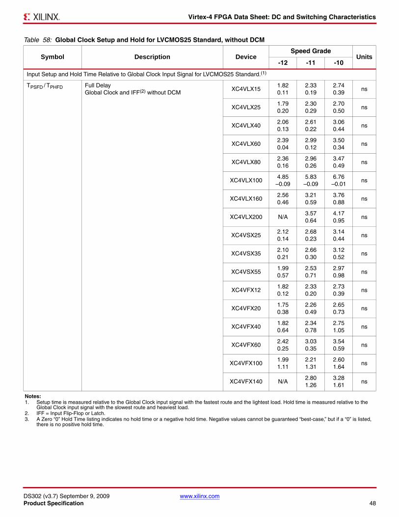
Virtex-4 FPGA Data Sheet: DC and Switching Characteristics
DS302 (v3.7) September 9, 2009 www.xilinx.comProduct Specification 48
Table 58: Global Clock Setup and Hold for LVCMOS25 Standard, without DCM
Symbol Description DeviceSpeed Grade
Units-12 -11 -10
Input Setup and Hold Time Relative to Global Clock Input Signal for LVCMOS25 Standard.(1)
TPSFD / TPHFD Full Delay Global Clock and IFF(2) without DCM
XC4VLX151.820.11
2.330.19
2.740.39
ns
XC4VLX251.790.20
2.300.29
2.700.50
ns
XC4VLX402.060.13
2.610.22
3.060.44
ns
XC4VLX602.390.04
2.990.12
3.500.34
ns
XC4VLX802.360.16
2.960.26
3.470.49
ns
XC4VLX1004.85
–0.095.83–0.09
6.76–0.01
ns
XC4VLX1602.560.46
3.210.59
3.760.88
ns
XC4VLX200 N/A3.570.64
4.170.95
ns
XC4VSX252.120.14
2.680.23
3.140.44
ns
XC4VSX352.100.21
2.660.30
3.120.52
ns
XC4VSX551.990.57
2.530.71
2.970.98
ns
XC4VFX121.820.12
2.330.20
2.730.39
ns
XC4VFX201.750.38
2.260.49
2.650.73
ns
XC4VFX401.820.64
2.340.78
2.751.05
ns
XC4VFX602.420.25
3.030.35
3.540.59
ns
XC4VFX1001.991.11
2.211.31
2.601.64
ns
XC4VFX140 N/A2.801.26
3.281.61
ns
Notes: 1. Setup time is measured relative to the Global Clock input signal with the fastest route and the lightest load. Hold time is measured relative to the
Global Clock input signal with the slowest route and heaviest load.2. IFF = Input Flip-Flop or Latch.3. A Zero “0” Hold Time listing indicates no hold time or a negative hold time. Negative values cannot be guaranteed “best-case,” but if a “0” is listed,
there is no positive hold time.
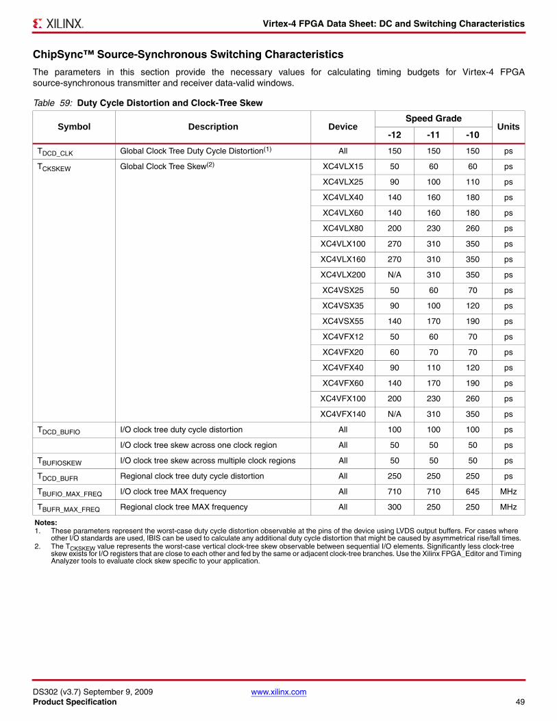
Virtex-4 FPGA Data Sheet: DC and Switching Characteristics
DS302 (v3.7) September 9, 2009 www.xilinx.comProduct Specification 49
ChipSync™ Source-Synchronous Switching Characteristics
The parameters in this section provide the necessary values for calculating timing budgets for Virtex-4 FPGAsource-synchronous transmitter and receiver data-valid windows.
Table 59: Duty Cycle Distortion and Clock-Tree Skew
Symbol Description DeviceSpeed Grade
Units-12 -11 -10
TDCD_CLK Global Clock Tree Duty Cycle Distortion(1) All 150 150 150 ps
TCKSKEW Global Clock Tree Skew(2) XC4VLX15 50 60 60 ps
XC4VLX25 90 100 110 ps
XC4VLX40 140 160 180 ps
XC4VLX60 140 160 180 ps
XC4VLX80 200 230 260 ps
XC4VLX100 270 310 350 ps
XC4VLX160 270 310 350 ps
XC4VLX200 N/A 310 350 ps
XC4VSX25 50 60 70 ps
XC4VSX35 90 100 120 ps
XC4VSX55 140 170 190 ps
XC4VFX12 50 60 70 ps
XC4VFX20 60 70 70 ps
XC4VFX40 90 110 120 ps
XC4VFX60 140 170 190 ps
XC4VFX100 200 230 260 ps
XC4VFX140 N/A 310 350 ps
TDCD_BUFIO I/O clock tree duty cycle distortion All 100 100 100 ps
I/O clock tree skew across one clock region All 50 50 50 ps
TBUFIOSKEW I/O clock tree skew across multiple clock regions All 50 50 50 ps
TDCD_BUFR Regional clock tree duty cycle distortion All 250 250 250 ps
TBUFIO_MAX_FREQ I/O clock tree MAX frequency All 710 710 645 MHz
TBUFR_MAX_FREQ Regional clock tree MAX frequency All 300 250 250 MHz
Notes: 1. These parameters represent the worst-case duty cycle distortion observable at the pins of the device using LVDS output buffers. For cases where
other I/O standards are used, IBIS can be used to calculate any additional duty cycle distortion that might be caused by asymmetrical rise/fall times. 2. The TCKSKEW value represents the worst-case vertical clock-tree skew observable between sequential I/O elements. Significantly less clock-tree
skew exists for I/O registers that are close to each other and fed by the same or adjacent clock-tree branches. Use the Xilinx FPGA_Editor and Timing Analyzer tools to evaluate clock skew specific to your application.

Virtex-4 FPGA Data Sheet: DC and Switching Characteristics
DS302 (v3.7) September 9, 2009 www.xilinx.comProduct Specification 50
Table 60: Package Skew
Symbol Description Device Package Value Units
TPKGSKEW Package Skew(1)
XC4VLX15SF363 80 ps
FF668 120 ps
XC4VLX25SF363 90 ps
FF668 110 ps
XC4VLX40FF668 110 ps
FF1148 150 ps
XC4VLX60FF668 130 ps
FF1148 140 ps
XC4VLX80 FF1148 155 ps
XC4VLX100FF1148 140 ps
FF1513 180 ps
XC4VLX160FF1148 145 ps
FF1513 180 ps
XC4VLX200 FF1513 180 ps
XC4VSX25 FF668 90 ps
XC4VSX35 FF668 100 ps
XC4VSX55 FF1148 145 ps
XC4VFX12SF363 90 ps
FF668 100 ps
XC4VFX20 FF672 110 ps
XC4VFX40FF672 120 ps
FF1152 150 ps
XC4VFX60FF672 110 ps
FF1152 170 ps
XC4VFX100FF1152 150 ps
FF1517 170 ps
XC4VFX140 FF1517 150 ps
Notes: 1. These values represent the worst-case skew between any two balls of the package: shortest flight time to longest flight time from Pad to Ball
(7.1 ps per mm).2. Package trace length information is available for these device/package combinations. This information can be used to deskew the package.

Virtex-4 FPGA Data Sheet: DC and Switching Characteristics
DS302 (v3.7) September 9, 2009 www.xilinx.comProduct Specification 51
Production SteppingThe Virtex-4 FPGA stepping identification system denotesthe capability improvement of production released devices.By definition, devices from one stepping are functionalsupersets of previous devices. Bitstreams compiled for adevice with an earlier stepping are guaranteed to operatecorrectly in subsequent device steppings.
New device steppings can be shipped in place of earlierdevice steppings. Existing production designs are guaran-teed on new device steppings. To take advantage of thecapabilities of a newer device stepping, customers are ableto order a new stepping version and compile a new bit-stream.
Production devices are marked with a stepping version, withthe exception of some step 1 devices. Designs should becompiled with a CONFIG STEPPING parameter set to aspecific stepping version. This parameter is set in the UCFfile:
CONFIG STEPPING = “#”; (where # is the stepping version)
The default stepping level used by the ISE software isreported in the PAR report.
Table 63 shows the JTAG ID code by step.
Table 61: Sample Window
Symbol Description DeviceSpeed Grade
Units-12 -11 -10
TSAMP Sampling Error at Receiver Pins(1) All 450 500 550 ps
TSAMP_BUFIO Sampling Error at Receiver Pins using BUFIO(2) All 350 400 450 ps
Notes: 1. This parameter indicates the total sampling error of Virtex-4 FPGA DDR input registers across voltage, temperature, and process. The
characterization methodology uses the DCM to capture the DDR input registers’ edges of operation. These measurements include:- CLK0 DCM jitter - DCM accuracy (phase offset)- DCM phase shift resolutionThese measurements do not include package or clock tree skew.
2. This parameter indicates the total sampling error of Virtex-4 FPGA DDR input registers across voltage, temperature, and process. The characterization methodology uses the BUFIO clock network and IDELAY to capture the DDR input registers’ edges of operation. These measurements do not include package or clock tree skew.
Table 62: ChipSync Pin-to-Pin Setup/Hold and Clock-to-Out
Symbol DescriptionSpeed Grade
Units-12 -11 -10
Data Input Setup and Hold Times Relative to a Forwarded Clock Input Pin Using BUFIO
TPSCS / TPHCS Setup/Hold of I/O clock across multiple clock regions–0.450.97
–0.451.08
–0.441.17
ns
Pin-to-Pin Clock-to-Out Using BUFIO
TICKOFCS Clock-to-Out of I/O clock across multiple clock regions 4.10 4.54 5.02 ns
Table 63: JTAG ID Code by Step
Device Step 0 Step 1 Step 2
XC4VLX15 3 5
XC4VLX25 9 A
XC4VLX40 3 5
XC4VLX60 2 or 3 4 or 5
XC4VLX80 3 5
XC4VLX100 2 or 3 4 or 5
XC4VLX160 0 or 3 4 or 5
XC4VLX200 0 or 3 2 or 5
XC4VSX25 2 4
XC4VSX35 2 4
XC4VSX55 2 4
XC4VFX12 0 or 2
XC4VFX20 2 6
XC4VFX40 0
XC4VFX60 2 8
XC4VFX100 0 6
XC4VFX140 0 4
Notes: 1. Shaded cells represent devices not produced at that stepping.

Virtex-4 FPGA Data Sheet: DC and Switching Characteristics
DS302 (v3.7) September 9, 2009 www.xilinx.comProduct Specification 52
Current Virtex-4 Production Devices
Table 64 summarizes the current production LX and SX device stepping.
Table 65 summarizes the current production FX device stepping.
Table 64: Current LX and SX Production Devices
LX/SX Device Stepping Step 1 Step 2
Example Ordering Code XC4VLX60-10FF672C XC4VLX60-10FF672CS2
Device steppings shipped when ordered per Example Ordering Code
Step 1 or Step 2 Step 2
Capability Improvements(1)
• The DFS macro is no longer needed
• TCONFIG requirement is removed
• DCM_RESET requirement is removed• DCM_INPUT_CLOCK_STOP requirement is
removed by a macro (automatically inserted by ISE software)
CONFIG STEPPING parameter (must be set in UCF file)
“1” “2”
Minimum Software Required ISE 7.1i SP4 ISE 7.1i SP4
Minimum Speed Specification Required.
1.58 1.58
Notes: 1. See LX and SX Errata for details on LX and SX Step 1 and ES silicon.
Table 65: Current FX Production Devices
FX Device Stepping Step 0 Step 1
Example Ordering Code XC4VFX60-10FF1152C XC4VFX60-10FF1152CS1
Device steppings shipped when ordered per Example Ordering Code
Step 0 or Step 1 Step 1
Capability Improvements See FX Errata for details
CONFIG STEPPING parameter (must be set in UCF file)
“0” “0” or “1”
Minimum Software Required ISE 8.1i SP2 ISE 8.1i SP2
Minimum Speed Specification Required
1.58 1.58
Notes: 1. Speed Specification v1.65 or later must be used for XC4VFX40 devices (all speed grades) and for XC4VFX100 (-12 speed grade only). In this case,
these family members (and speed grades) are released to production before a speed specification is released with the correct label (Advance, Preliminary, or Production). These labeling discrepancies will be corrected in a subsequent speed specification release.
Virtex-4 FPGA Data Sheet: DC and Switching Characteristics
DS302 (v3.7) September 9, 2009 www.xilinx.comProduct Specification 53
Revision HistoryThe following table shows the revision history for this document.
Date Version Revisions
08/02/04 1.0 Initial Xilinx release. Printed Handbook version.
09/09/04 1.1 Edits in Tables 12, 13, 18, 19, 20, 22, 26, 28, 37, and 38. Removed Table 39.
01/18/05 1.2 Added parameters to Tables 4 and 5. Removed System Monitor and ADC parameters.
02/01/05 1.3 Changed parameters in Tables 1, 2, 3, 7, and 11. Added Interface Performance Characteristics section. Added Switching Characteristics section and Table 14. Added parameters to the following tables: 4–6, 14, 16–30, 32–40, and 46.
02/24/05 1.4 Changed the notes in Table 2. Added Set/Reset parameters to Table 32 and Table 33. Changed description in Table 35. Changed Set/Reset in Table 37. Changed PSCLK units in Table 45. Added parameters to Table 46. Changed DCM_TAP_MS_MIN in Table 50.
05/19/05 1.5 Added RocketIO and PowerPC parameters to Table 1, Table 2, and Table 3. Removed conditions from VIDIFF and VICM in Table 9. Revised Table 13. Added RocketIO DC Input and Output Levels section. Added PowerPC Switching Characteristics section. Added RocketIO Switching Characteristics section. Removed Table 31 from version 1.4. Revised Table 35. Along with changes to Table 43 and Table 50, there are three new requirements to ensure maximum operating frequencies for the DCM. Added parameters to Table 54, Table 55, Table 56, Table 58, Table 59, Table 60, Table 61, Table 62.
06/17/05 1.6 Revised VIN and VTS in Table 1 and Note 4. Revised typical PCPU specification in Table 3. Revised symbols and values in the Processor tables: Table 16 through Table 22. Revised TDCREF in Table 24. Corrected the CLKOUT_FREQ_FX_HF_MS_MIN in Table 45, the CLKOUT_FREQ_FX_LF_MR_MIN in Table 46, and the “Input Clock Period Jitter” in Table 47. Corrected units in Table 59.
06/27/05 1.7 Changed VIL and VIH for LVCMOS15 in Table 7. Revised Table 14. Replaced value for VEYEin Table 25. Added Note 4 to Table 50. Added Table 57: Global Clock Setup and Hold forLVCMOS25 Standard, with DCM in Source-Synchronous Mode. Added value forXC4VLX160-FF1513 in Table 60. Added values for -12 speed specifications to most of thetables. Revised the -10 and -11 speeds in most of the switching characteristics tables.
08/06/05 1.8 Updated to speed specification v1.56. Added VCC_CONFIG note to Table 2. Clarified design information in Table 13. Corrected TPROGRAM in Table 43. Added DRP configuration timing for DCMs to Table 43. Added global clock tree maximum frequency to Table 44. Corrected CLKOUT_FREQ_FX_LF_MS_MIN in Table 45. Added footnotes 3 and 4 to Table 45 and Table 46. Added more data to the TCKSKEW in Table 59.
08/29/05 1.9 Corrected VOCM in Table 8. Revised Table 11. Added RocketIO MGT Clock DC Input Levels to Table 12. Revised SFI-4.1 performance values in Table 13. Added software tools requirements ISE7.1i SP4, to description above Table 14. Added -11X speed grade to Table 14 and Table 23. Edited Table 15 and Table 16. Edited Table 24. Added note 2 to Table 25, and moved RXOOBVDPP to Table 12. Added conditions to TDJ and TRJ in Table 26. Moved TXOOBVDPP to Table 12. Added RSDS to Table 27. Added note 4 to Table 49. Added Production Stepping section.
09/28/05 1.10 Table 2: Removed Note 1. Recommended maximum voltage drop for VCCAUX is 10 mV/ms.

Virtex-4 FPGA Data Sheet: DC and Switching Characteristics
DS302 (v3.7) September 9, 2009 www.xilinx.comProduct Specification 54
02/03/06 1.11 Revised the speed specification requirements in Switching Characteristics, page 12, with parameter changes in Table 54 and Table 56. Added Note 7 to Table 2. Added to the IRPU and IRPD specifications in Table 3. Changed LVCMOS18 to meet the JEDEC specification in Table 7. Inserted notes into Table 8, Table 9, and Table 10. Corrected note 1 in Table 11. In Table 12, revised Common Mode Input Voltage Range (VICM) typical from 800 mV to 600 mV and added a new Note 1. Also in Table 12, changed Common Mode Voltage specification from 95mV to 950mV. Changed performance numbers in Table 23. Removed the typical specification for TDJ from Table 26. Added note 2 to Table 27. In Table 35, added maximum to TIDELAYCTRLCO_RDY, and a new parameter TIDELAYPAT_JIT. Revised Note 1 in Table 43. Added note 5 to Table 45. Revised notes 3 and 5 in Table 50. Changed the CLKIN_FREQ_PMCD_CLKA_MAX -12 specification in Table 53. Changed the TBUFIO_MAX_FREQ specification in Table 59. Changed the information in the Production Stepping and Current Virtex-4 Production Devices sections.
03/22/06 1.12 Modified second paragraph in Power-On Power Supply Requirements. Added/Changed numbers for ICCINTMIN, ICCAUXMIN, and ICCOMIN, and added Note 2 (Table 5). Changed the typ value of the DC Parameter, Common Mode Input Voltage Range from 600 MV to 800 MV in Table 12. Added three DC parameters to Table 12, Input Common-Mode Voltage (VICMC), Peak-to-Peak Differential Input Voltage (VIDIFF), and Differential Input Resistance (RIN). Changed the SPI4.2 entry for -11 from 900 Mb/s to 1 Gb/s in Table 13. Added Note 3 to Table 15. Reduced the maximum frequency from 322 MHz to 250 MHz (in Table 25 and Table 26). Added Note 5 to Table 40.
06/01/06 1.13 Changed VIN and VTS values and added notes to Table 1, page 1. Removed -11X speed grade from Table 14. Updated to speed specification v1.60. Removed -11X speed grade, changed the -12 and -11 speed grade to 6.5 Gb/s, and deleted Note 1 in Table 23, page 16. Deleted first condition and changed second condition to 2.5 Gb/s to 6.5 Gb/s for Reference Clock total jitter, peak-peak (TGJTT) in Table 24, page 16. Changed the max value for Serial data rate FGTX to 6.5 Gb/s. Deleted first condition and changed second condition to 2.5 Gb/s to 6.5 Gb/s for Serial data output deterministic jitter (TDJ) and deleted first condition and changed second condition to 2.5 Gb/s to 6.5 Gb/s for Serial data output random jitter (TRJ), both in Table 26, page 18.
06/23/06 1.14.1 Virtex-4 FPGA Electrical Characteristics, page 1: removed paragraph on that introduced the -11x for XC4VFX devices. Table 3, page 3: added new values for ICCAUXRX, ICCAUXTX, ICCCAUXMGT, ITTX, ITRX, and new notes 2 and 3. Table 4, page 4: added new symbols and for values ICCAUXRX, ICCAUXTX, ITTX , ITRX,IAUMGT and new notes 4 and 5. Table 12, page 11: changed DC parameters and values and added note. Table 14: changed speed designations for the XC4VFX devices. Table 24, page 16 and Table 25, page 17, for most characteristics: changed conditions, speed grade (typ and max) values, and units. Table 26, page 18, for most characteristics: changed conditions, speed grade (typ and max) values, and units. Updated notes. Table 43, page 36: removed the Tcnfig symbol, values, and note 1. Note 2 is now Note 1, and the reference has also been changed. Table 50, page 42: removed Input Signal Requirements. Table 54, page 44, Table 55, page 45, Table 56, page 46, Table 57, page 47, and Table 58, page 48: corrected large speed numbers to N/A.
08/23/06 1.15 Table 24, page 16: changed value for Reference Clock Rise/Fall Time (TRCLK; TFCLK) from 65 ps Typ to 400 ps Max. Table 35, page 29: changed the speeds specification for the -12, -11, and -10 Speed Grades for TIDELAYRESOLUTION, deleted row for TIDELAYRESOLUTION_ERR and added row for TIDELAYTOTAL_ERR. Table 39, page 32: changed the speeds specification for -12 Speed Grades, Sequential Delay characteristics: TREG, TREGXB, TREGYB, TCKSH, and TREGF5. Table 65, page 52: added stepping information for Virtex-4 FX devices.
Date Version Revisions

Virtex-4 FPGA Data Sheet: DC and Switching Characteristics
DS302 (v3.7) September 9, 2009 www.xilinx.comProduct Specification 55
09/07/06 1.16 Added 2.5V rows to VIN and VTS (Table 1, page 1). Updated value DVIN from 200 mV to 110 mV in Table 12, page 11. Updated speed grade specifications for XCV4FX devices in Table 14. Updated jitter tolerance and VEYE in Table 25, page 17. Corrected equation for TIDELAYTOTAL_ERR in Table 35, page 29.
10/06/06 1.17 • SPEED SPECIFICATION version for this data sheet release: v1.62.• Table 1: Removed former note 3 on VIN.
• Table 14: Moved XC4VFX12-11, XC4VFX20-11, XC4VFX60-11, and XC4VFX100-11 devices to Production status.
• Table 15: Expanded to break out processor clock specifications into Characteristics when APU Not Used and Characteristics when APU Used. Removed specs for CPMFCMCLK, not available.
• Table 25, Table 26: Updated RX and TX jitter data and notes.• Table 39: Modified TREGXB, TREGYB, and TCKSH timing parameters to comply with
v1.62 speed specification.
12/11/06 2.0 • SPEED SPECIFICATION version for this data sheet release: v1.62.• Table 1: Modified Note (3) referring to 3.3V I/O design guidelines. Added IIN
parameters.• Table 2: Corrected recommended VTRX range to 0.25V – 2.5V. Added IIN parameters.
• Table 7: Added LVDCI attributes with LVCMOS.• Table 13: Added Note (1) for SDR LVDS Interface requiring AC coupling above
622 MHz. Added DDR2 SDRAM (High-Performance SERDES Design) with reference to XAPP721. Updated all specification values.
• Pin-to-Pin Performance and Register-to-Register Performance tables (formerly Table 13 and Table 14) deleted.
• Table 14: XC4VFX12 changed to Production status.• Table 15: Added APU-used max characteristics for -12 devices.• Table 24: Added values for Spread-Spectrum Clocking and footnote.• Table 26: Changed symbol for jitter parameters from TJ, RJ, and DJ to TJ, RJ, and DJ
respectively.• Table 32: Added Note (1) to refer to Timing Report for non-zero tap values. Made DLY
setup/hold parameters relative to C, not CLKDIV.• Table 34: Amended Note (1) to refer to Timing Report for non-zero tap values.• Table 35: Added Note (1) to refer to XAPP707 for details on IDELAY timing
characteristics. Changed TIDELAYRESOLUTION from 74 ps to 75 ps to match Timing Analyzer. Modified formula for TIDELAYTOTAL_ERR to use 75 ps resolution.
• Table 40: Added CLK-to-DOUT parameters for “with ECC” case. Added CLK-to-CLK parameter.
• Table 43, Table 44, Table 59: Added configuration parameter values for -12 speed grade.
• Table 45: Added FMAX for -12 speed grade.
• Table 45, Table 46, Table 47: Added Note (6) stating that CLKIN values for DLL only also apply to DLL and DFS together.
• Table 46, Table 47: Replicated Note (5) from Table 45 and applied to all CLKIN with DLL parameters.
• Table 47, Table 50: Added notes to clarify boundary-frequency cases.• Table 48: Modified Note (1) to point to the architecture wizard for CLKFX output jitter.
Added Note (2) to indicate that PMCD outputs introduce no jitter.
Date Version Revisions

Virtex-4 FPGA Data Sheet: DC and Switching Characteristics
DS302 (v3.7) September 9, 2009 www.xilinx.comProduct Specification 56
12/11/06(Cont’d)
2.0(Cont’d)
• Table 50: Removed T_LOCK_FX_MIN parameter. Added DCM_RESET.• Table 53: Added Note (1), no minimum frequency for PMCD.• Table 64: Added Note (1) to refer to LX and SX Errata for capability improvements.
03/27/07 2.1 • SPEED SPECIFICATION version for this data sheet release: v1.64.• Table 4: Added Note (6) regarding max quiescent supply current.• Table 5: Filled in missing power-on current values for FX devices.• Table 24: Added new parameter FGREFCLK. Added Min value for Spread Spectrum
Clocking frequency. Corrected “Conditions”. • Table 26: Revised Notes (2) and (3).• Table 37, Table 38: Added column/values for XC4VFX -12.• Table 39: Added columns/values for XC4VFX -11 and -12. Corrected XC4VLX/SX -11
and -12 values for TREGXB, TREGYB, and TCKSH.
• Table 43: Restored parameter TCONFIG and footnote (1) from earlier revision. Added new parameter TSMCO (SelectMAP Readback Clock-to-Out).
• Table 50: Restored DCM_RESET Minimum and DCM_INPUT_CLOCK_STOP parameters from earlier revision. Added Notes (4) through (7) to these parameters.
• Table 60: Removed FF1760 package. Not supported.• Table 63: Added FX devices and JTAG IDs.
06/08/07 2.2 • SPEED SPECIFICATION version for this data sheet release: v1.65.• Table 14: Promoted -12 speed grade devices of XC4VFX12, XC4VFX20, and
XC4VFX60 to Production status.• Table 37: Removed parameter TISCCK_REV. Not meaningful because pin should always
be connected to GND.• Table 43: Added parameter FMAX_SELECTMAP. for maximum Slave SelectMAP mode
external configuration clock frequency.• Table 63: Filled in Step 1 values for XC4VFX20, XC4VFX60, and XC4VFX100.• Table 65: Added Step 1 data.
08/10/07 2.3 • SPEED SPECIFICATION version for this data sheet release: v1.65.• Table 3: Added MAX value for IBATT .
• Table 25: Added unit (ns) to RXSIGDET.• Table 27: Added Note (3) specifying range of DCI reference resistors and referring to
UG070.• Added section Ethernet MAC Switching Characteristics, page 22, and replaced
Table 29.• Added section I/O Standard Adjustment Measurement Methodology, page 23,
including Table 30, Table 31, and Figure 4.• Table 43: Added parameter FMAX_ICAP. Added word “Data” to description of
SelectMAP Setup/Hold.• Table 64: Added to Capability Improvements, for Step 1 that the DFS macro is no
longer needed.
09/10/07 2.4 • SPEED SPECIFICATION version for this data sheet release: v1.67.• Table 14: Promoted all speed grades for XC4VFX40 devices, and -12 speed grade for
XC4VFX100 devices, to Production status.• Table 63: Filled in Step 1 value for XC4VFX40.• Table 65: Added Note 1.
Date Version Revisions
Virtex-4 FPGA Data Sheet: DC and Switching Characteristics
DS302 (v3.7) September 9, 2009 www.xilinx.comProduct Specification 57
09/28/07 3.0 • SPEED SPECIFICATION version for this data sheet release: v1.67.• Promoted data sheet to Production status.• Table 14: Moved XC4VFX140, all speed grades, from Advance to Production status.• Table 59: Added/updated all Global Clock Tree Skew values. Qualified Note (2) by
adding “vertical”.• Table 60: Added Package Skew values for XC4VFX40, XC4VFX100, and XC4VFX140.• Table 63: Added JTAG ID code for XC4VFX140.
12/11/07 3.1 • SPEED SPECIFICATION version for this data sheet release: v1.68.• Added new copyright notice and legal disclaimer section.• Table 13: Removed table note references to XAPP700, XAPP704, and XAPP705
(obsolete). Renumbered table notes.• Table 15: Added new Note 1, renumbered subsequent table notes.• Table 30: Removed table rows for LVPECL_33, LVDS_33, and LVDSEXT_33.• Table 30, Table 31: Corrected “electron-coupled” to “emitter-coupled”.• Table 31: For LVDS Extended Mode 2.5V, corrected I/O Standard Attribute to
LVDSEXT_25.• Table 37: Added Note 4 specifying FTOG for -11 FX devices as 1181 MHz.
• Table 43: Added parameter FMAX_READBACK.
• Table 58: Corrected TPSFD for XC4VFX100 devices to 1.99 ns.
• Section Production Stepping, page 51: Advised that current stepping level is reported by the ISE tool in the PAR report.
04/10/08 3.2 • SPEED SPECIFICATION version for this data sheet release: v1.68.• Table 28, page 22: Re-inserted table.• Table 43, page 36: Updated Symbol names for the DRP entries.• Table 63, page 51: Revised code for XC4VFX40 package to 0.
06/06/08 3.3 • SPEED SPECIFICATION version for this data sheet release: v1.68.• Table 3, page 3: In Note (2), clarified differences between settings for typical and
maximum ICC numbers.
• Table 24, page 16: Revised FGCLK to show different maximum frequencies depending on the speed grade. Removed TPHASE.
• Table 35, page 29: Reorganized according to IDELAYCTRL and IDELAY.
11/26/08 3.4 • Table 35, page 29: Added FMAX.
06/16/09 3.5 • Table 40, page 33: Changed TRCKO_DOA to a Max parameter.
08/13/09 3.6 • Table 3, page 3: Updated Note 1.• Table 45, page 38: Added Note 6 reference to and updated descriptions of
CLKIN_FREQ_DLL_HF_MS_MIN and CLKIN_FREQ_FX_HF_MS_MAX.
09/09/09 3.7 • Table 7, page 8: Added “LVCMOS” to Notes 3 and 4.
Date Version Revisions

Virtex-4 FPGA Data Sheet: DC and Switching Characteristics
DS302 (v3.7) September 9, 2009 www.xilinx.comProduct Specification 58
Notice of DisclaimerTHE XILINX HARDWARE FPGA AND CPLD DEVICES REFERRED TO HEREIN (“PRODUCTS”) ARE SUBJECT TO THE TERMS ANDCONDITIONS OF THE XILINX LIMITED WARRANTY WHICH CAN BE VIEWED AT http://www.xilinx.com/warranty.htm. THIS LIMITEDWARRANTY DOES NOT EXTEND TO ANY USE OF PRODUCTS IN AN APPLICATION OR ENVIRONMENT THAT IS NOT WITHIN THESPECIFICATIONS STATED IN THE XILINX DATA SHEET. ALL SPECIFICATIONS ARE SUBJECT TO CHANGE WITHOUT NOTICE.PRODUCTS ARE NOT DESIGNED OR INTENDED TO BE FAIL-SAFE OR FOR USE IN ANY APPLICATION REQUIRING FAIL-SAFEPERFORMANCE, SUCH AS LIFE-SUPPORT OR SAFETY DEVICES OR SYSTEMS, OR ANY OTHER APPLICATION THAT INVOKESTHE POTENTIAL RISKS OF DEATH, PERSONAL INJURY, OR PROPERTY OR ENVIRONMENTAL DAMAGE (“CRITICALAPPLICATIONS”). USE OF PRODUCTS IN CRITICAL APPLICATIONS IS AT THE SOLE RISK OF CUSTOMER, SUBJECT TOAPPLICABLE LAWS AND REGULATIONS.