xilinx zynq-7000 epp - hot chips epp devices z-7010 z-7020 z-7030 z-7040 processing system processor...
TRANSCRIPT

© Copyright 2009 Xilinx Copyright 2011 Xilinx
Vidya Rajagopalan, Vamsi Boppana, Sandeep Dutta, Brad Taylor, Ralph Wittig
August 18, 2011
Xilinx Zynq-7000 EPP An Extensible Processing Platform Family

© Copyright 2009 Xilinx Copyright 2011 Xilinx Copyright 2011 Xilinx
Zynq-7000 EPP Architecture & Silicon
Zynq-7000 Software & Applications
Agenda
Page 2
Xilinx Series 7 Highlights
Summary

© Copyright 2009 Xilinx Copyright 2011 Xilinx Copyright 2011 Xilinx
Xilinx 7 Series Highlights
7 Series silicon devices
– 28 nm Technology, TSMC HPL process
– 50% reduction in power over 40 nm devices
3 FPGA Fabrics
– Artix = Low cost, low power FPGA (“1W FPGA”)
– Kintex = Density & performance FPGA (“Market Sweet spot”)
– Virtex = Highest density and performance FPGA
(“More than Moore”)
‘More than Moore’ density increase
– Up to 2M logic cells
– Using Stacked Silicon Interconnect Technology (SSIT)
Improved GT bandwidth
– GT bandwidth increased to 28 GHz
Zynq Embedded Processing Platform (EPP)
Page 3
Design GreenDesign Green by XilinxDesign GreenDesign Green by Xilinx

© Copyright 2009 Xilinx Copyright 2011 Xilinx Copyright 2011 Xilinx
Silicon Interposer
Microbumps
Through‐Silicon Vias
Page 4
More Than Moore Xilinx Stacked Silicon Interconnect Technology
Package Substrate
28nm FPGA Slice 28nm FPGA Slice 28nm FPGA Slice 28nm FPGA Slice
C4 Bumps
BGA Balls
Microbumps • Access to power / ground / IOs • Access to logic regions • Leverages ubiquitous image sensor
micro-bump technology Through-silicon Vias (TSV) • Only bridge power / ground / IOs to C4 bumps
• Coarse pitch, low density aids manufacturability • Etch process (not laser drilled)
Side-by-Side Die Layout • Minimal heat flux issues
• Minimal design tool flow impact
Passive Silicon Interposer (65nm Generation) • 4 conventional metal layers connect micro bumps & TSVs
• No transistors means low risk and no TSV induced performance degradation

© Copyright 2009 Xilinx Copyright 2011 Xilinx Copyright 2011 Xilinx
Zynq-7000 EPP Architecture & Silicon
Zynq-7000 Software & Applications
Agenda
Page 5
Xilinx Series 7 Highlights
Summary
© Copyright 2009 Xilinx Copyright 2011 Xilinx
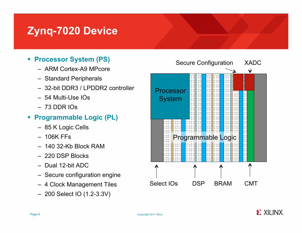
Zynq-7020 Device
Page 6
Processor System (PS)
– ARM Cortex-A9 MPcore
– Standard Peripherals
– 32-bit DDR3 / LPDDR2 controller
– 54 Multi-Use IOs
– 73 DDR IOs
Programmable Logic (PL)
– 85 K Logic Cells
– 106K FFs
– 140 32-Kb Block RAM
– 220 DSP Blocks
– Dual 12-bit ADC
– Secure configuration engine
– 4 Clock Management Tiles
– 200 Select IO (1.2-3.3V)
Processor
System
Select IOs CMT BRAM DSP
XADC Secure Configuration
Processor System
Programmable Logic

© Copyright 2009 Xilinx Copyright 2011 Xilinx Copyright 2011 Xilinx
Zynq-7000 Device Family
Zynq-7000 EPP Devices Z-7010 Z-7020 Z-7030 Z-7040
Pro
ce
ss
ing
Sy
ste
m
Processor Core Dual ARM® Cortex™-A9 MPCore™
Processor Extensions NEON™ & Single / Double Precision Floating Point
Max Frequency 800MHz
Memory L1 Cache 32KB I / D, L2 Cache 512KB, on-chip Memory 256KB
External Memory Support DDR3, DDR2, LPDDR2, 2x QSPI, NAND, NOR
Peripherals 2x USB 2.0 (OTG), 2x Tri-mode Gigabit Ethernet,
2x SD/SDIO, 2x UART, 2x CAN 2.0B, 2x I2C, 2x SPI, 4x 32b GPIO
Pro
gra
mm
ab
le
Lo
gic
Approximate ASIC Gates ~430K (30k LC) ~1.3M (85k LC) ~1.9M (125k LC) ~3.5M (235k LC)
Extensible Block RAM 240KB 560KB 1,060KB 1,860KB
Peak DSP Performance (Symmetric FIR) 58 GMACS 158 GMACS 480 GMACS 912 GMACS
PCI Express® (Root Complex or Endpoint) - Gen2 x4 Gen2 x8
Agile Mixed Signal (XADC) 2x 12bit 1Msps A/D Converter
I/O
Processor System IO 130
Multi Standards 3.3V IO 100 200 100 200
Multi Standards High Performance 1.8V IO - - 150 150
Multi Gigabit Transceivers - - 4 12
Page 7

© Copyright 2009 Xilinx Copyright 2011 Xilinx Copyright 2011 Xilinx
CAN (2)
GigE (2)
USB (2)
SDIO (2)
I2C (2)
SPI (2)
UART (2)
Cortex A9
NEON
32KB I$/D$
Cortex A9
NEON
32KB I$/D$
SCU
Timers, AWDT, GIC, ACP
L2 Cache
512KB
OCM
256 KB
DMA TTC SWDT
Parallel
CTRL
DDR
CTRL
Quad‐SPI
CTRL
NAND
CTRL
Config
Coresight
AMBA AXI Interconnect
Processing System
Security
Config
XADC
GTs
Select IO
PCIe
Programmable
Logic
PLL(3)
General Purpose ACP High Performance
Zynq 7000 EPP
GPIO
Zynq-7000 Processor System (PS)
Dual Core Cortex ARM A9
– NEON, 512 KB L2 cache
– 256 KB On-Chip-Memory (OCM)
DDR Interface
– DDR3 Performance
– High BW utilization
Config & Legacy Memory I/F
– Quad-SPI, NOR, NAND
Standard Peripherals – GigE …
– Available to PS IO or to Programmable
Logic
System Level Peripherals
– Clock generation, Counter Timers
– 8 Channel DMA controller
– Coresight Debugging
Page 8
LPDDR2
DDR2
DDR3 32-bit
MIO[53:0]
PS Peripherals can be multiplexed onto 54 external Multi-Use-IOs
(MIO)
PS Peripherals can also be routed through the Programmable Logic
NOR
NAND
Quad-SPI

© Copyright 2009 Xilinx Copyright 2011 Xilinx Copyright 2011 Xilinx
CAN (2)
GigE (2)
USB (2)
SDIO (2)
I2C (2)
SPI (2)
UART (2)
Cortex A9
NEON
32KB I$/D$
Cortex A9
NEON
32KB I$/D$
SCU
Timers, AWDT, GIC, ACP
L2 Cache
512KB
OCM
256 KB
DMA TTC SWDT
Parallel
CTRL
DDR
CTRL
Quad‐SPI
CTRL
NAND
CTRL
Config
Coresight
AMBA AXI Interconnect
Processing System
Security
Config
XADC
GTs
Select IO
PCIe
Programmable
Logic
PLL(3)
General Purpose ACP High Performance
Zynq 7000 EPP
GPIO
Zynq-7000 Programmable Logic (PL)
Programmable Logic Resources
– 30K – 235 K Logic Cells
– Dedicated 36 K-bit BRAMs, DSP, CMT
– XADC dual channel 12-bit ADC
– Up to 12 GTs with PCIe hard core
– Up to 300 Select IOs
Programmable Logic AXI Interfaces
– Multiple 32/64 bit AXI interfaces to PL
– Accelerator Coherency Port (ACP) with
access to caches
Programmable Logic System Interfaces
– Interrupts, DMA control
– Debug
High Performance PL Configuration
– Security Decryption Engine
– Under 200 ms configuration time from flash
– Debugging interfaces
Page 9
4-8 GB/sec
DDR3 32-bit

© Copyright 2009 Xilinx Copyright 2011 Xilinx
Customizing Zynq Tools for the Programmable Logic System Builder
Clocking
– Flexible clock sources (PS or PL)
– Simple clock interfaces
Memory and Peripheral access
– PL access to all memory: Caches, OCM, DDR
– 2 dedicated DDR ports ensure bandwidth
– PL access to all peripherals in PS
Interconnect
– AXI Interconnect IP available from Xilinx
– Optimized for FPGA implementation
Debug and Misc.
– Bidirectional cross-triggers (Coresight and Chipscope)
– 16 general purpose interrupts from PL to PS
Page 10
0.0
0.5
1.0
1.5
2.0
2.5
3.0
0% 20% 40% 60% 80% 100%
Re
lati
ve
La
ten
cy
DDR Utilization
Zynq-7000 DDR Utilization vs Latency
D Q
Q D
To PL
From PL
PL clock
Simple Clock Interfaces

© Copyright 2009 Xilinx Copyright 2011 Xilinx
SW managed Programmable Logic (PL) Linux based, “remote controlled”, programmable logic
Page 11
SW user experience:
SoC with integrated PL
Configure PL (full and partial)
Start/stop & single step clocks
Setup & update HW triggers
Monitor HW performance counters
Observe & sync to PL hardware events
clocks
ARM Coresight
Cross Trigger
H/W Events
Config
PS PL

© Copyright 2009 Xilinx Copyright 2011 Xilinx Copyright 2011 Xilinx
Zynq-7000 Power Saving Features
Low power 1.0V HPL 28 nm process silicon technology
Programmable Logic can be powered off and on as needed
– 40-90% reduction in static power depending on device
– Very fast configuration times when loaded from DRAM
Low power ARM Cortex-A9 MP
– Incorporates clock gating and power-down modes
Support for LPDDR2 devices
– Ultra low power self refresh
Peripherals shutdown
Page 12
Design GreenDesign Green by XilinxDesign GreenDesign Green by Xilinx

© Copyright 2009 Xilinx Copyright 2011 Xilinx Copyright 2011 Xilinx
Engineering Insights Process Selection Criteria
Page 13
Process Considerations:
28 HP: Highest Performance HKMG Process
(but must be able to afford power; e.g. GPU)
28 HPL: Low power HKMG process
(shifts down HP power / performance range)
28 LP: No HKMG low power process
(cheaper than HPL, but less performance)
Xilinx’ Reasons for Selecting HPL:
Higher performance than LP
(at same power level)
Higher performance vs HP at FPGA TDP
(or lower power at same performance)
Po
we
r
Frequency
Frequency
Po
we
r

© Copyright 2009 Xilinx Copyright 2011 Xilinx Copyright 2011 Xilinx
Engineering Insights Finding The Frequency Sweet Spot (within the HPL Process)
Page 14
0.50
1.00
1.50
2.00
450 550 650 750
Normalized Power vs. Frequency
Vt usage
High Vt
Med Vt
Low Vt
Worst Setup
-40c
Hold
Typical
Timing Histograms
0
1
2
Max Nom Min
Normalized Path Delay
Delay Variation

Copyright 2011 Xilinx
Engineering Insights Configuring Interconnect
15
CPU
800 MHz
FPGA
200 Mhz
Switch OCM
400 MHz
CPU:
FPGA:
OCM:
1
1 1 1 1
1 2
1 1 1 1 1 1
1
1 2
3
3 -stalled-
2 2
CPU
800 MHz
FPGA
200 Mhz
Switch OCM
400 MHz
Threshold
CPU:
FPGA:
OCM:
1
1 1 1 1
1 2
1 1 1 1 2 2 2 1 1
1 3
2 1 1 3
release
1
Copyright 2011 Xilinx
© Copyright 2009 Xilinx Copyright 2011 Xilinx Copyright 2011 Xilinx
Zynq-7000 EPP Architecture & Silicon
Zynq-7000 Software & Applications
Agenda
Page 16
Xilinx Series 7 Highlights
Summary
© Copyright 2009 Xilinx Copyright 2011 Xilinx Copyright 2011 Xilinx
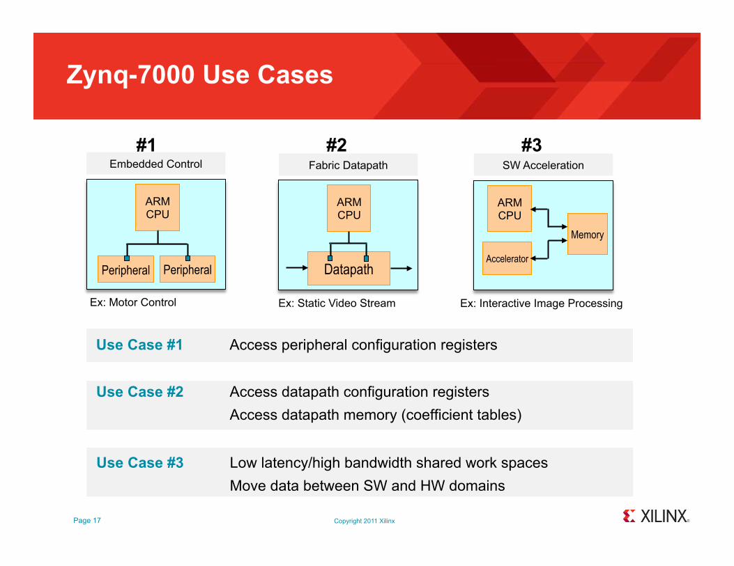
Zynq-7000 Use Cases
Page 17
SW Acceleration
Peripheral Peripheral
ARM CPU
Datapath
ARM CPU
ARM CPU
Accelerator
Memory
Fabric Datapath Embedded Control
#1 #2 #3
Use Case #1 Access peripheral configuration registers
Use Case #2 Access datapath configuration registers
Access datapath memory (coefficient tables)
Use Case #3 Low latency/high bandwidth shared work spaces
Move data between SW and HW domains
Ex: Motor Control Ex: Static Video Stream Ex: Interactive Image Processing

© Copyright 2009 Xilinx Copyright 2011 Xilinx Copyright 2011 Xilinx
Application Programming Using Only C
Application
C/C++
Video Codec CPU
Encryption
LTE Modem Memory Da
ta M
ov
em
en
t In
terc
on
ne
ct
FPGA Fabric
SW-Centric Design Environment
Binary for CPU Bitstream for PL fabric
Device Information
High-Level Synthesis
via AutoESL

© Copyright 2009 Xilinx Copyright 2011 Xilinx Copyright 2011 Xilinx
AutoESL Generated Accelerators C-Based, High-Level Synthesis Tools at Xilinx
Page 19
Application Example: Back Projection Algorithm (recreate CT scan images from samples)
gprof Locate SW hot spot function(s) on ARM
AutoESL Synthesize hot spot function(s) to HW/PL
52 Floating Point Operators @ 200Mhz
Fits in lowest cost Zynq 7010 device
3X Performance vs SW only

© Copyright 2009 Xilinx Copyright 2011 Xilinx Copyright 2011 Xilinx
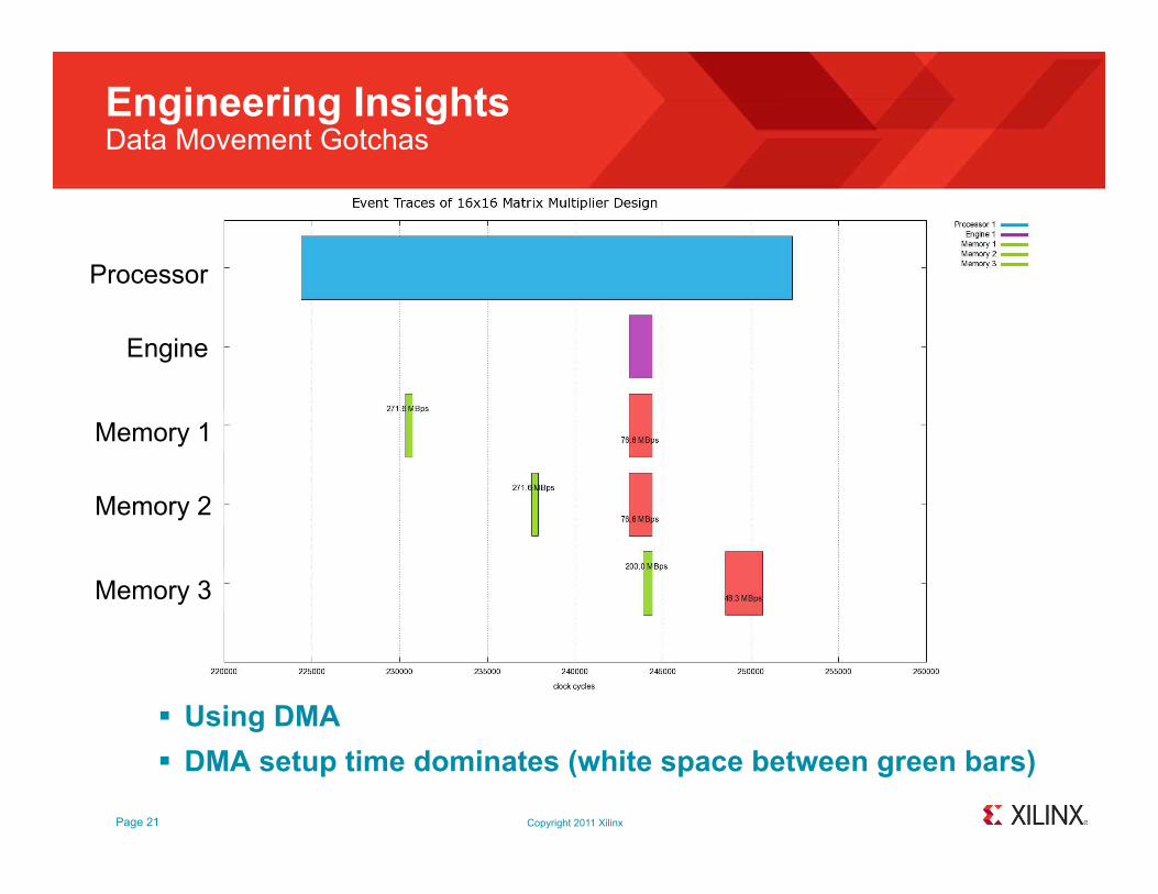
Engineering Insights Data Movement Gotchas
Page 20
Using CPU Programmed IO
IO dominates accelerator compute time
Processor
Engine
Memory 1
Memory 2
Memory 3
Host Program
Matrix Mult
© Copyright 2009 Xilinx Copyright 2011 Xilinx Copyright 2011 Xilinx
Engineering Insights Data Movement Gotchas
Page 21
Using DMA
DMA setup time dominates (white space between green bars)
Processor
Engine
Memory 1
Memory 2
Memory 3

© Copyright 2009 Xilinx Copyright 2011 Xilinx Copyright 2011 Xilinx
Xilinx Evolution Towards Multicore
Page 22
Logic
BRAM
DSP
Dual
A9
Next Gen
GPP
MC Array
PE
PE
PE
PE
acc1
acc2
acc2
acc1
Multicore programming models being ported to Zynq
Legacy
ZYNQ
“Future Zynq”
Glue
GPP + Accelerators
GPP + Multicore +
Soft Processing Engine + Accelerators
uB acc1
acc2 MicroBlaze Soft Multi-Core + Accelerators
uB

© Copyright 2009 Xilinx Copyright 2011 Xilinx Copyright 2011 Xilinx
Zynq 7000 EPP Architecture & Silicon
Zynq 7000 Software & Applications
Agenda
Page 23
Xilinx Series 7 Highlights
Summary

© Copyright 2009 Xilinx Copyright 2011 Xilinx Copyright 2011 Xilinx
Summary
Zynq SoC Device Family
with Integrated Programmable Logic
$15 Price Point* / 28nm Fab Process
Microcontroller and Accelerator Use Models
Industry Standard Tools
(ARM Ecosystem, Android, ISE)
Emerging Tools (AutoESL, Multicore)
Emulation platforms in use for prototyping
Available 1H 2012
Page 24
* High volume price for smallest device and package, slowest speed grade
Android on Zynq emulation board
Source: iVeia LLC