xps for non-destructive depth profiling and 3d imaging of
TRANSCRIPT

REVIEW
XPS for non-destructive depth profiling and 3D imagingof surface nanostructures
Shaaker Hajati & Sven Tougaard
Received: 5 September 2009 /Revised: 10 December 2009 /Accepted: 14 December 2009 /Published online: 21 January 2010# Springer-Verlag 2010
Abstract Depth profiling of nanostructures is of highimportance both technologically and fundamentally. There-fore, many different methods have been developed fordetermination of the depth distribution of atoms, forexample ion beam (e.g. O2
+, Ar+) sputtering, low-damageC60 cluster ion sputtering for depth profiling of organicmaterials, water droplet cluster ion beam depth profiling,ion-probing techniques (Rutherford backscattering spec-troscopy (RBS), secondary-ion mass spectroscopy (SIMS)and glow-discharge optical emission spectroscopy(GDOES)), X-ray microanalysis using the electron probevariation technique combined with Monte Carlo calcula-tions, angle-resolved XPS (ARXPS), and X-ray photoelec-tron spectroscopy (XPS) peak-shape analysis. Each of thedepth profiling techniques has its own advantages anddisadvantages. However, in many cases, non-destructivetechniques are preferred; these include ARXPS and XPSpeak-shape analysis. The former together with parallelfactor analysis is suitable for giving an overall understand-ing of chemistry and morphology with depth. It works verywell for flat surfaces but it fails for rough or nanostructuredsurfaces because of the shadowing effect. In the lattermethod shadowing effects can be avoided because only asingle spectrum is used in the analysis and this may betaken at near normal emission angle. It is a rather robustmeans of determining atom depth distributions on the
nanoscale both for large-area XPS analysis and for imaging.We critically discuss some of the techniques mentionedabove and show that both ARXPS imaging and, particular-ly, XPS peak-shape analysis for 3D imaging of nano-structures are very promising techniques and open agateway for visualizing nanostructures.
Keywords Nanostructures . XPS peak-shape analysis .
Depth profiling . 3D imaging
Introduction
Several methods are in use for the determination of the depthdistribution of atoms. These include ion-beam (e.g. O2
+, Ar+)sputtering [1, 2], low-damage C60 cluster ion sputtering fordepth profiling of organic materials [3–5], water dropletcluster ion beam depth profiling [6], ion-probing techniques(Rutherford backscattering spectroscopy (RBS), secondary-ion mass spectroscopy (SIMS), and glow-discharge opticalemission spectroscopy (GDOES)) [7], X-ray microanalysisusing the electron probe variation technique combined withMonte Carlo calculations [8], angle-resolved XPS (ARXPS)[9], and X-ray photoelectron spectroscopy (XPS) peak-shapeanalysis [10–15]. For depths >5–10 nm, sputter depthprofiling, where atoms are removed by bombardment withenergetic inert gas ions (usually Ar+), is a widespread andeffective technique. It is a destructive technique and effectssuch as the preferential sputtering of one type of atomcompared with another, intermixing, and radiation-enhanceddiffusion, combine to limit the resulting depth resolution. Inaddition, there is the problem of the reduction of somespecies to lower oxidation states.
Other techniques are therefore used to achieve accurateanalysis of the surface composition of the outermost few
S. Hajati (*)Department of Physics, Yasouj University,Yasouj 75918-74831, Irane-mail: [email protected]: [email protected]
S. TougaardDepartment of Physics and Chemistry,University of Southern Denmark,5230 Odense M, Denmark
Anal Bioanal Chem (2010) 396:2741–2755DOI 10.1007/s00216-009-3401-9

nanometers. ARXPS has been used for more than 30 yearsas a technique for non-destructive analysis of surfacestructures [9] and a facility for this analysis is available inmost software. It relies on the angular dependence of thepeak intensity; in other words, the greater the angle of take-off into the analyzer with respect to the surface normal, theshallower the depth z from which photoelectrons areaccepted (Eq. 1). In an excellent paper by Cumpson [16],the limitations, the problems, and the accuracies that can beachieved with this method were investigated systematicallyfrom a theoretical point of view. Parallel systematicexperimental investigations to determine the limitations ofARXPS have, unfortunately, not been performed except forspecific systems such as SiO2 on Si [17].
Another technique, developed by Tougaard et al. [10–15,18, 19], relies on the fact (Figs. 1 and 5) that the inelasticbackground in the energy distribution of emitted electronsdepends strongly on the depth concentration profile. Therange of validity of this method has been studiedextensively both theoretically and experimentally [15].
Angle-resolved XPS (ARXPS)
The ARXPS formalism is founded on a simple expressionthat relates the measured photoelectron intensity to theconcentration profile, f(z) viz:
IA qð Þ ¼ I0R10
CF z; qð Þ f ðzÞ exp � zl cos q
� �dz
ffi I0R10
f ðzÞ exp � zl cos q
� �dz
ð1Þwhere I0 1 cosθ is the intensity recorded from a referencesample with f(z) = 1. The factor CF(z, θ) accounts for
elastic electron-scattering effects [20]. In the last expres-sion, on the right, elastic collisions have been neglected sothat CF=1. Elastic scattering may be important for θ>60°or if most of the detected electrons originate from layers z>21 . A correction for this is implemented in some software(see, e.g., Ref. [21]).
By measuring the intensity for different values of θ, thedepth profile f(z) can in principle be determined by comparisonwith Eq. 1. Several numerical procedures have been suggested[9] for inversion of Eq. 1 and thus for direct determination of f(z) but they tend to be unstable and in practice a simple trial-and-error procedure is usually preferred, where f(z) is changeduntil a good match of Eq. 1 to experiments recorded for a fewvalues of θ is obtained. This procedure is usually executedsemi-automatically by the software. Inverse Laplace transformof the angular profile IA(θ) can give f(z) but, as Cumpsondescribes [16], this inversion is extremely sensitive to smallerrors in the peak intensities.
The most serious limitation of this method is that it worksonly for very flat surfaces because if the surface is not flat,there is a shadowing effect for large θ. In general, the use oflarge values of θ cannot be avoided because cos θ varies onlyslightly with θ for small θ. It is therefore necessary to includemeasurements at θ larger than about 50° to obtain gooddepth information. So for rough surfaces the interpretation ofARXPS is complicated because the angular variation of theXPS peak intensity will depend on the surface roughness.Even for ideally flat substrates, ARXPS analysis of laterallyinhomogeneous surface structures grown on the surface isquite complex. The reason is that neighboring nanoclustersshadow the XPS peak intensity for large θ. The effectdepends on both the shape and distribution of clusters on thesurface. This is hard to correct for and ARXPS analysis maythen become quite unreliable. The problem was addressedrecently in detail [22–24]. For crystalline solids, measure-ments in high-symmetry directions should be avoided,because forward photoelectron focusing effects can lead to20–30% variations in peak intensity which (if they areincluded in the analysis) lead to large errors.
Quantification of elemental depth distribution by ARXPSis however straightforward and quite accurate for perfectlyflat surfaces of amorphous solids. It is applied widely to thestudy of thin SiO2 layers on Si and has been shown to workvery well for this particular system [17], because thesesurfaces can be made extremely flat. Furthermore the lightelements Si and O are weak elastic scatterers, so accuratecorrection for elastic electron scattering is not so important.ARXPS is also useful in quantification of thin polymer filmsand carbonaceous contamination layers.
Traditional XPS analysis relies on XPS peak intensityassuming that the concentration in the surface region isproportional to the XPS peak intensity. There are limitations tothis and it is known that more information than that typical
Fig. 1 Au 4d spectra measured from a thin gold layer on top of anickel substrate (I) and after evaporation of different amounts of nickelon top (II–V). From Ref. [15]
2742 S. Hajati, S. Tougaard
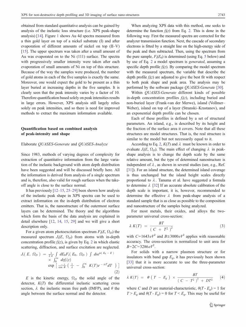
obtained from standard quantitative analysis can be gained byanalysis of the inelastic loss structure (i.e. XPS peak-shapeanalysis) [14]. Figure 1 shows Au 4d spectra measured froma thin gold layer on top of a nickel substrate (I) and afterevaporation of different amounts of nickel on top (II–V)[15]. The upper spectrum was taken after a small amount ofAu was evaporated on to the Ni (111) surface. The spectrawith progressively smaller intensity were taken after eachevaporation of small amounts of Ni on top of this structure.Because of the way the samples were produced, the numberof gold atoms in each of the five samples is exactly the same.Moreover, one would expect the gold to be present as a thinlayer buried at increasing depths in the five samples. It isclearly seen that the peak intensity varies by a factor of 10.Therefore quantification based solely on peak intensities resultsin large errors. However, XPS analysis still largely reliessolely on peak intensities, and so there is need for improvedmethods to extract the maximum information available.
Quantification based on combined analysisof peak-intensity and shape
Elaborate QUASES-Generate and QUASES-Analyze
Since 1983, methods of varying degrees of complexity forextraction of quantitative information from the large varia-tion of the inelastic background with atom depth distributionhave been suggested and will be discussed briefly here. Allthe information is derived from analysis of a single spectrumand is, therefore, also valid for rough surfaces when the take-off angle is close to the surface normal.
It has previously [12–15, 25–29] been shown how analysisof the inelastic peak shape in XPS spectra can be used toextract information on the in-depth distribution of electronemitters. That is, the nanostructure of the outermost surfacelayers can be determined. The theory and the algorithmswhich form the basis of the data analysis are explained indetail elsewhere [12, 14, 15, 29] and we will give a shortdescription only.
For a given atom photoexcitation spectrum Fi(E, ΩD) themeasured spectrum Ji(E, ΩD) from atoms with in-depthconcentration profile fi(z), is given by Eq. 2 in which elasticscattering, diffraction, and surface excitation are neglected.
Ji E; ΩDð Þ ¼ 12 p
RdE0Fi E0; ΩDð Þ R
dseis E0 � Eð Þ
� R10 dzfiðzÞ
exp � zcos q
1l � R1
0 KðTÞe � isT dT� �� �
ð2ÞE is the kinetic energy, ΩD the solid angle of the
detector, K(T) the differential inelastic scattering crosssection, 1 the inelastic mean free path (IMFP), and θ theangle between the surface normal and the detector.
When analyzing XPS data with this method, one seeks todetermine the function fi(z) from Eq. 2. This is done in thefollowing way. First the measured spectra are corrected for theanalyzer transmission function. Next, the cascade of secondaryelectrons is fitted by a straight line on the high-energy side ofthe peak and then subtracted. Then, using the spectrum fromthe pure sample, Fi(E0) is determined (using Eq. 5 below) andby use of Eq. 2 a model spectrum is generated, assuming aspecific depth profile fi(z). By comparing the model spectrumwith the measured spectrum, the variable that describe thedepth profile fi(z) are adjusted to give the best fit with respectto both peak shape and peak area. The analysis may beperformed by the software package QUASES-Generate [30].
Within QUASES-Generate different kinds of possiblein-depth concentration profiles fi(z), including buried andnon-buried layer (Frank-van der Merwe), island (Vollmer–Weber), island on top of a layer (Stranski–Krastanov), andan exponential depth profile can be chosen.
Each of these profiles is defined by a set of structuralparameters. An island, e.g., is described by its height andthe fraction of the surface area it covers. Note that all thesestructures are model structures. That is, the real structure issimilar to the model but not necessarily equal to it.
According to Eq. 2, K(T) and 1 must be known in order toevaluate Ji(E, ΩD). The main effect of changing 1 in peak-shape analysis is to change the depth scale by the samerelative amount, but the type of determined nanostructure isindependent of 1 , as shown in several studies (see, e.g., Ref.[31]). For an island structure, the determined island coverageis thus unchanged but the island height scales directlyproportional to 1 . Tanuma et al. have suggested a formulato determine 1 [32] If an accurate absolute calibration of thedepth scale is important, it is, however, recommended todetermine the effective 1 from peak-shape analysis of astandard sample that is as close as possible to the compositionand nanostructure of the samples being analyzed.
For most metals, their oxides, and alloys the two-parameter universal cross-section:
l KðTÞ ¼ BT
C þ T2ð Þ2 ð3Þ
with C=1643eV2 and B≅3000eV2 applies with reasonableaccuracy. The cross-section is normalized to unit area forB=2C=3286eV2.
For solids with a narrow plasmon structure or forinsulators with band gap Eg, it has previously been shown[33] that it is more accurate to use the three-parameteruniversal cross-section:
l KðTÞ ¼ q T � Eg
� � � BT
C � T2ð Þ2 þ DT 2ð4Þ
where C and D are material-characteristic, θ(T - Eg) = 1 forT > Eg and θ(T - Eg) = 0 for T < Eg. This may be useful for
XPS for non-destructive depth profiling and 3D imaging of surface nano-structures 2743
silicon dioxide (Eg≅9eV) and the polymers (Eg≅2–6eV).The correction for band gap, where present, will only havea limited effect and only for analysis of the near-peakregion.
If the analyzed peaks do not overlap in energy, it is oftenbetter to apply the so-called ‘Tougaard-background’ removalto determine the undistorted spectrum F(E, ΩD). This has theadvantage that the primary excitation spectrum, F(E, ΩD),does not necessarily need to be known. The analysis relieson the formulas:
F E; ΩDð Þ ¼ 1
P1J E; ΩDð Þ � 1
2 p
ZdE0 J E0; ΩDð Þ
�
�Z
dse � is E � E0ð Þ 1 � p1PðsÞ
� � �
ð5Þwhere
PðsÞ ¼Z
f ðzÞe � zcos q
P ðsÞdz; P1 ¼
Z 1
0f ðzÞe � z
l cos q dz;
ð6Þwith
XðsÞ ¼ 1
l�
Z 1
0KðTÞe−isTdT ð7Þ
Now P1 ¼ lims ! � 1 PðsÞ and 1−P1/P(s)→0 fors→∞. The function 1 − P1/P(s) is therefore suitable fordiscrete Fourier transformation. Then the integral over s inEq. 5 may be evaluated numerically by fast Fouriertransformation. The remaining integral over E′ and theintegral over z may be evaluated by standard numericalmethods. In this way, the original excitation spectrumcorrected for inelastically scattered electrons F(E, ΩD) isdetermined. Equation 5 may be used to determine either F(E,
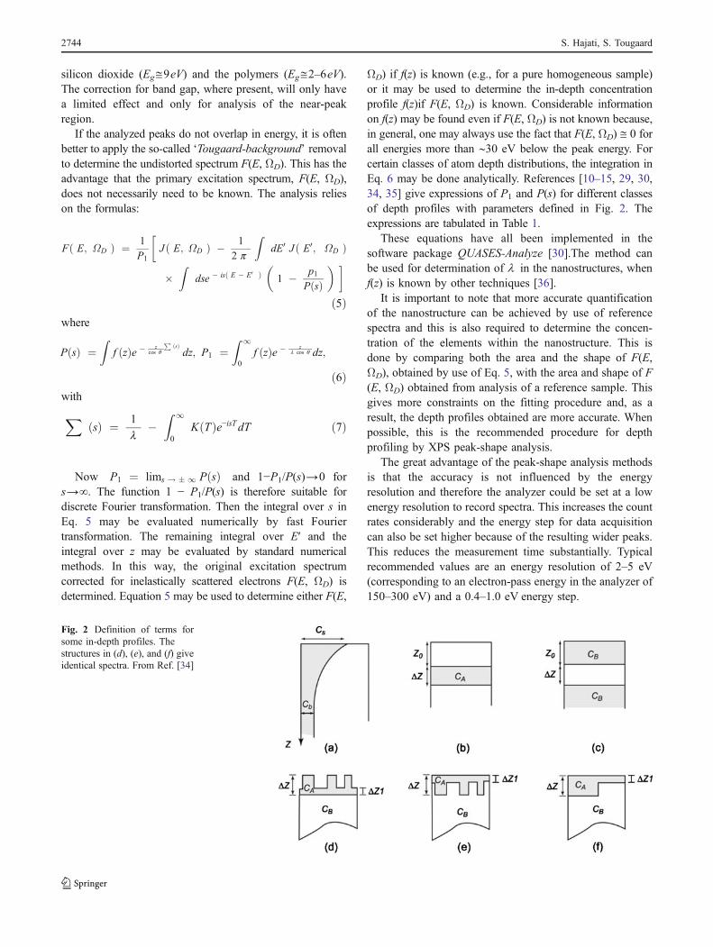
ΩD) if f(z) is known (e.g., for a pure homogeneous sample)or it may be used to determine the in-depth concentrationprofile f(z)if F(E, ΩD) is known. Considerable informationon f(z) may be found even if F(E, ΩD) is not known because,in general, one may always use the fact that F(E, ΩD) ≅ 0 forall energies more than ∼30 eV below the peak energy. Forcertain classes of atom depth distributions, the integration inEq. 6 may be done analytically. References [10–15, 29, 30,34, 35] give expressions of P1 and P(s) for different classesof depth profiles with parameters defined in Fig. 2. Theexpressions are tabulated in Table 1.
These equations have all been implemented in thesoftware package QUASES-Analyze [30].The method canbe used for determination of 1 in the nanostructures, whenf(z) is known by other techniques [36].
It is important to note that more accurate quantificationof the nanostructure can be achieved by use of referencespectra and this is also required to determine the concen-tration of the elements within the nanostructure. This isdone by comparing both the area and the shape of F(E,ΩD), obtained by use of Eq. 5, with the area and shape of F(E, ΩD) obtained from analysis of a reference sample. Thisgives more constraints on the fitting procedure and, as aresult, the depth profiles obtained are more accurate. Whenpossible, this is the recommended procedure for depthprofiling by XPS peak-shape analysis.
The great advantage of the peak-shape analysis methodsis that the accuracy is not influenced by the energyresolution and therefore the analyzer could be set at a lowenergy resolution to record spectra. This increases the countrates considerably and the energy step for data acquisitioncan also be set higher because of the resulting wider peaks.This reduces the measurement time substantially. Typicalrecommended values are an energy resolution of 2–5 eV(corresponding to an electron-pass energy in the analyzer of150–300 eV) and a 0.4–1.0 eV energy step.
Fig. 2 Definition of terms forsome in-depth profiles. Thestructures in (d), (e), and (f) giveidentical spectra. From Ref. [34]
2744 S. Hajati, S. Tougaard
Tab
le1
Exp
ressions
ofP1andP(s)fordifferentclassesof
depthprofilesshow
nin
Fig.2
Depth
distribu
tionfunctio
nf(z)
P1,P(s)
Cs�
Cb
ðÞexp
�z L
�� þ
Cb
P1
¼Cbl icos
qþ
Cs�
Cb
ðÞ
Ll icos
qLþ
l icos
q
PðsÞ
¼Cbcos
qΣ
ðsÞþ
Cs�
Cb
ðÞ
Lcos
qLΣ
ðsÞþ
cos
q
Nδ(z−z 0)
P1
¼N
exp
�z 0
lcos
q
��
PðsÞ
¼N
exp
�z 0
ΣðsÞ
cos
q
f AðzÞ
¼0
for
0<
z<
z 0CA
for
z 0<
z<
z 0þ
Δz
0for
z 0þ
Δz<
z
8 > > < > > :P1
¼CAl icos
q:exp
�z 0
l icos
q
1�
exp
�Δ
zlcos
q
��
��
PðsÞ
¼CAcos
qΣ
ðsÞexp
�z 0
ΣðsÞ
cos
q
1�
exp
�Δ
zΣ
ðsÞcos
q
hi
f BðzÞ
¼CB
for
0<
z<
z 00
for
z 0<
z<
z 0þ
Δz
CB
for
z 0þ
Δz<
z
8 > > < > > :P1
¼C
Bl icos
q1
�exp
�z 0
l icos
q
1�
exp
�Δ
zl icos
q
hi
no
PðsÞ
¼CBcos
qΣ
ðsÞ1
�exp
�z 0
ΣðsÞ
cos
q
1�
exp
�Δ
zΣ
ðsÞcos
q
hi
no
f AðzÞ
¼CA
for
0<
z<
Δz 1
f 1CA
for
Δz 1
<z
<Δ
z0
for
Δz<
z
8 > > < > > :P1
¼CAl icos
q1
�1
�f 1
ðÞexp
�Δ
z 1l icos
q
�
f 1exp
�Δ
z 1l icos
q
no
PðsÞ
¼CAcos
qΣ
ðsÞ1
�1
�f 1
ðÞexp
�Δ
z 1Σ
ðsÞcos
q
�
f 1exp
�Δ
z 1Σ
ðsÞcos
q
no
f BðzÞ
¼0
for
0<
z<
Δz 1
1�
f 1ð
ÞCB
for
Δz 1
<z
<Δ
zCB
for
Δz<
z
8 > > < > > :P1
¼CBlcos
q1
�f 1
ðÞexp
�Δ
z 1l icos
q
�
f 1exp
�Δ
zl icos
q
no
PðsÞ
¼CBcos
qΣ
ðsÞ1
�f 1
ðÞexp
�Δ
z 1Σ
ðsÞcos
q
�
f 1exp
�Δ
zΣ
ðsÞcos
q
no
XPS for non-destructive depth profiling and 3D imaging of surface nano-structures 2745
Shadowing effects for rough surfaces and increasedimportance of elastic scattering effects and surfaceexcitations which might cause some errors for largeemission angles may, to a large extent, be avoided in thepeak-shape analysis method. To this end, it is thereforerecommended to measure the spectra at an emission anglenot too far (preferably <45°) from the surface normal. Ifthe sample is crystalline, one should use large analyzeracceptance angles and avoid angles of high crystallinesymmetry, because forward focusing effects are largest inthese directions.
The XPS-peak-shape method is non-destructive andtherefore also allows one to study the change in surfacecomposition during surface treatment as, e.g., in chemicalreactions and gradual annealing. It has been applied bymany research groups in the study of a wide range ofsystems and physical phenomena, including growth mech-anisms and nanostructures of metal/metal [25–27, 37–43],metal/silicon [28, 44, 45], metal/germanium [45], germani-um/silicon [46–49], InxGa1− xAs films [50], amorphousa-Si1− xCx:H alloys [51], polymer systems [52–54], metal-nanoparticle/HOPG [55], metal-nanoparticle/Al2O3 [56],metal–nanoparticle/polymer systems [57], C-segregationon Ni [41], metal oxide growth [15, 58–64], SiO2 films[31, 65], nucleation of ZnTe on As-terminated Si [66], andthe depth excitation function in electron stimulated AES[67, 68]. Some of these were reviewed in Ref. [15]. Severaltests on the validity of the method have also been done bycomparing with other techniques, for example AFM [43,47–49, 54], RBS [31, 37, 48], ISS [63], ellipsometry [31],ARXPS [31, 53], RBS [31, 37], quartz-crystal microbal-ance (QCM) [25, 38, 42, 57], RHEED [66], TEM [57],XTEM [42] and use of Synchrotron radiation with varyingphoton energy [40, 69, 70].
Applications of QUASES-Generate
To use Eqs. 5–7, minimal interference of neighboring linesacross a wide spectral range is required. This could be alimitation for that method. However, QUASES-Generatehas been used to handle this limitation. Simonsen et al.successfully used QUASES-Generate for depth profiling thenanostructure of Ge deposited on Si(001) [46]. Graat et al.[58, 71] used it to determine the depth distributions ofdifferent iron oxide structures where overlapping peaks arepresent. QUASES-Generate was also applied by Grosvenoret al. [59, 60]. Jussila et al. investigated the morphologyand composition of nanoscale surface oxides on Fe-20Cr-18Ni{111} austenitic stainless steel [72] and the initialstages of surface oxidation of Fe-17Cr (ferritic stainlesssteel) [73]. Schleberger [74] used the method to investigateamorphous Fe/Ge/Fe structure and to see to what extent theinterface between the metal and the semiconductor is sharp.
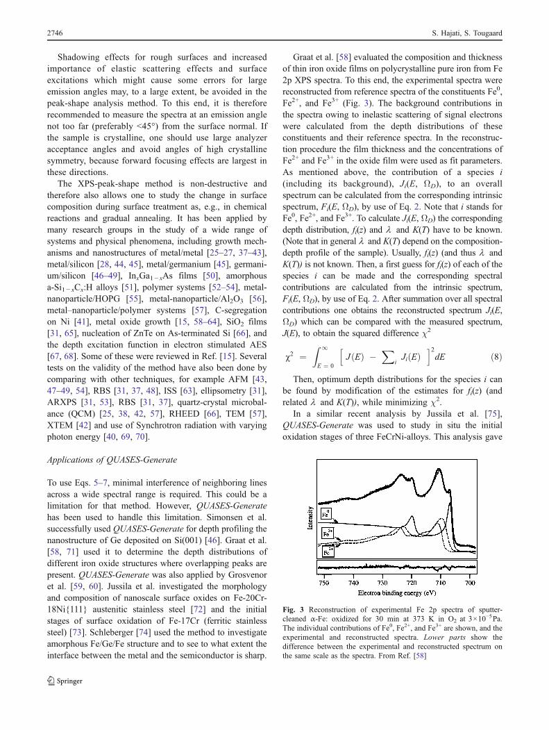
Graat et al. [58] evaluated the composition and thicknessof thin iron oxide films on polycrystalline pure iron from Fe2p XPS spectra. To this end, the experimental spectra werereconstructed from reference spectra of the constituents Fe0,Fe2+, and Fe3+ (Fig. 3). The background contributions inthe spectra owing to inelastic scattering of signal electronswere calculated from the depth distributions of theseconstituents and their reference spectra. In the reconstruc-tion procedure the film thickness and the concentrations ofFe2+ and Fe3+ in the oxide film were used as fit parameters.As mentioned above, the contribution of a species i(including its background), Ji(E, ΩD), to an overallspectrum can be calculated from the corresponding intrinsicspectrum, Fi(E, ΩD), by use of Eq. 2. Note that i stands forFe0, Fe2+, and Fe3+. To calculate Ji(E, ΩD) the correspondingdepth distribution, fi(z) and 1 and K(T) have to be known.(Note that in general 1 and K(T) depend on the composition-depth profile of the sample). Usually, fi(z) (and thus 1 andK(T)) is not known. Then, a first guess for fi(z) of each of thespecies i can be made and the corresponding spectralcontributions are calculated from the intrinsic spectrum,Fi(E, ΩD), by use of Eq. 2. After summation over all spectralcontributions one obtains the reconstructed spectrum Ji(E,ΩD) which can be compared with the measured spectrum,J(E), to obtain the squared difference χ2
#2 ¼Z 1
E ¼ 0JðEÞ �
XiJiðEÞ
h i2dE ð8Þ
Then, optimum depth distributions for the species i canbe found by modification of the estimates for fi(z) (andrelated 1 and K(T)), while minimizing χ2.
In a similar recent analysis by Jussila et al. [75],QUASES-Generate was used to study in situ the initialoxidation stages of three FeCrNi-alloys. This analysis gave
Fig. 3 Reconstruction of experimental Fe 2p spectra of sputter-cleaned α-Fe: oxidized for 30 min at 373 K in O2 at 3×10⁻⁵Pa.The individual contributions of Fe0, Fe2+, and Fe3+ are shown, and theexperimental and reconstructed spectra. Lower parts show thedifference between the experimental and reconstructed spectrum onthe same scale as the spectra. From Ref. [58]
2746 S. Hajati, S. Tougaard

quite detailed information on the depth distribution ofnanostructures of Fe and Cr oxides after O2 exposure.
Applications of QUASES-Analyze
As mentioned above, peak-shape analysis using the QUASESsoftware package has been successfully used in the study ofa wide range of system and physical phenomena [15, 25–28,31, 37–45, 47–56, 61–68]. In a recent XPS peak-shapeanalysis by Kisand et al. [76] the morphology and thicknessof ultrathin films of KCl on Copper were estimated.
Schleberger et al. investigated amorphous Fe/Si and Fe/Ge nanostructures by analyzing wide range spectra of theFe3p and Fe2p from the overlayer and SiKLL and GeLMMfrom the substrate [45]. It was shown that XPS peak-shapeanalysis could be used to determine the morphology ofsurface nanostructures by analyzing signals from eitheroverlayer or substrate. This is an advantage of the method,i.e, even in case acquiring a spectrum with a good signal-to-noise ratio is possible from only the substrate and notfrom the overlayer it is still possible to characterize theoverlayer by analyzing spectrum from the substrate.
Interface effects in the Ni2p XPS spectra of NiO thinfilms grown on different oxide substrates, namely SiO2,Al2O3 and MgO, were quantitatively studied by Preda et al.[77] by using XPS peak-shape analysis.
Recently, Gonzalez-Elipe et al. have used the method todescribe the size and shape of the nuclei of several oxidesgrown on different substrates [63, 78–84], e.g. supportedzirconia nanoparticles on SiO2, Y2O3, and CeO2 [85]. Thecharacterization of these nuclei is important because theirsize, shape, and dispersion degree on the surface are criticalfor the control of the microstructure of the thin films. Theinterest of this type of analysis is not limited to thin-filmnucleation as in the example of supported zirconia nano-particles, but can be of interest for other situations whereknowledge of the shape and size of supported particles maybe important (e.g., catalysts, supported nanoparticles, etc.).In this regard, it is interesting to recall that in manyexperimental situations it is not possible to assess theparticle size and shape of deposited nanoparticles by meansof classical microscopy methods. This is the case when,with materials with a high electron density or high surfaceroughness, electron microscopy or atomic force microscopyfails to differentiate the structures of a support from those ofthe supported nanoparticles. It is believed that in these casesXPS peak-shape analysis can be very useful for a morpho-logical characterization of supported nanoparticles [85].
Wetting properties of poly(ethylene terephthalate) (PET)and low-density polyethylene polymers were investigatedby the method after treatment with a microwave (MW)plasma discharge at low pressure and a dielectric barrierdischarge at atmospheric pressure. The oxygen distribution
between the topmost surface layer and the bulk wasobtained [86] by non-destructive XPS peak-shape analysis.
In all of these studies, different classes of depth profilesillustrated in Fig. 2 were used. Recently Hajati et al. [57]applied the method to study how gold nanoclusters grow,diffuse and distribute in polystyrene as a function of bothcluster size and temperature in the range from below toabove the glass transition temperature of the polymer. Thestudy was done by considering the profile shown in Fig. 2fand setting ΔZ1=0. To make it applicable to determinationof the size and density of Au nanoclusters, each sphericalnanocluster (with diameter 2R and surface coverage f1) wasdivided into nine coaxial cylindrical shells with the samesurface coverage and different height. The size (2R) of thenanoclusters was then adjusted to subtract the inelasticbackground from the measured spectrum (Fig. 4) and thesurface coverage was adjusted to fit the backgroundsubtracted spectrum to the reference spectrum F(E, ΩD).
In this way, the size and density of Au nanoclusters weredetermined for four different amounts of gold deposition.
It is noted here that although in Ref. [57] the shape of thenanocluster was modeled as a sphere using multiple islandsof varying height, the analysis is not sensitive enough todiscriminate between a sphere and a cube as long as thevolume is identical (this is actually also mentioned in Ref.[57] but is worth stressing in this context because the figuresin Ref. [57] might give this impression). With peak-shapeanalysis, only the three primary properties that describe themain characteristics of the nanostructure are determined withhigh accuracy, see also Ref. [15]. In this case these threeparameters were the gold coverage, height, and concentra-tion. All information can, however, be deduced from thedetermined island height and coverage. Thus, taking theheight as the nanocluster diameter, the nanocluster densitycan readily be calculated from the coverage.
Fig. 4 Analyzed Au 4f spectrum for 24Å gold at room temperature.From Ref. [57]
XPS for non-destructive depth profiling and 3D imaging of surface nano-structures 2747

The results obtained are in excellent agreement with QCMand TEM. The authors also successfully studied the gradualembedding of the Au clusters as the temperature was raised.The method can thus give this detailed quantitative informa-tion on such a metalized polymer without the need for anyother complimentary and time-consuming technique such asAFM, TEM, and XTEM. It is also important to note that thisinformation is obtained very quickly from analysis of a singleXPS spectrum and that the changes can be followed in almostreal time by sequentially measuring the XPS as the growth ortemperature-induced effects happen.
Peak area-to-background ratio Ap/B
The simplest quantitative description of the variation inpeak shape and background with depth is to take the ratio
of the peak area Ap to the increase in background height Bat a chosen energy below the peak energy. This ratio is verysensitive to the in-depth distribution because Ap and B varyin opposite directions as a function of the depths of theatoms in a solid. For homogeneous distribution of atoms ithas been shown that this ratio, D0, is fairly constant(∼23 eV), independently of material and peak energy.Substantial deviations from this value can then be used toestimate the depth distribution of atoms [10, 87].
The algorithm can be defined from Fig. 5. Ap is the peakarea (of the doublet in this case) determined after a linearbackground has been subtracted (dashed line) from themeasured spectrum. The upper energy point to be chosen forthe straight line background is taken to be the energy atwhich the spectral intensity is 10% of that at the peak energy,while the low energy point at the other end of the straightline is defined as being at the same distance below the peakenergy as the high energy point is above it [10]. B is theincrease in intensity measured 30 eV below the peak energy.(In the case, as here, of a doublet peak, the geometricalweighted centroid of the peak structure is used as referenceenergy). A quick estimate of the in-depth distribution ofatoms can then be found from the rules in Table 2. For agiven system, the method may be fine-tuned by calibratingD0 against Ap/B determined from the analysis of a sampleknown to have a homogeneous atom distribution. Anexample of its application is also shown in Fig. 5, wherethe values Ap/B are seen to be consistent with the rules inTable 2. Other examples of its practical application byJohansson et al. may be found in Refs. [88, 89]. Recently,Perring et al. used it to determine the depth distribution of Fatoms in an assembly of organic monolayers on polydicy-clopentadiene [90] and it was also used by Walton et al. toobtain images of oxide film thickness (SiOx/Si) after noisereduction by principal-component analysis [91].
3D XPS nano-imaging
As seen in the section “ Elaborate QUASES-Generate andQUASES-Analyze”, the elaborated method for XPS peak-shape analysis is quite accurate and rather easy to apply.However, it requires operator interaction, and is therefore
Fig. 5 Two examples of the application of the Ap/B and decay length(L) methods. The two model spectra were calculated for (a) a goldsubstrate covered with a 3.0 nm overlayer and (b) a 1.5 nm gold filmon top of a substrate. 1 =1.5 nm in both cases. From Ref. [34]
Table 2 Rules for estimating the depth profile from Ap/B. From Refs. [10, 87]
Ap/B Depth distribution
∼23 eV Uniform
>30 eV Surface localized
<20 eV Subsurface localized
If the same peak from two samples has the values D1 ¼ Ap=B� �
1and D2 ¼ Ap=B
� �2
then:
if 30 eV<D1<D2 Atoms are surface localized in both samples and are at shallower depths in sample 2 than in sample 1
if D1<D2<20 eV Atoms are primarily in the bulk of both samples and at deeper depths in sample 1 than in sample 2
2748 S. Hajati, S. Tougaard
not practical for XPS imaging where thousands of spectramust be analyzed.
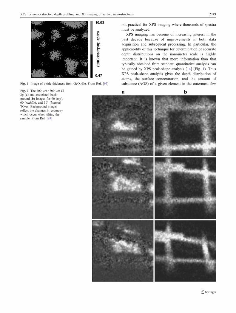
XPS imaging has become of increasing interest in thepast decade because of improvements in both dataacquisition and subsequent processing. In particular, theapplicability of this technique for determination of accuratedepth distributions on the nanometer scale is highlyimportant. It is known that more information than thattypically obtained from standard quantitative analysis canbe gained by XPS peak-shape analysis [14] (Fig. 1). ThusXPS peak-shape analysis gives the depth distribution ofatoms, the surface concentration, and the amount ofsubstance (AOS) of a given element in the outermost fewFig. 6 Image of oxide thickness from GeO2/Ge. From Ref. [97]
Fig. 7 The 700 μm×700 μm Cl2p (a) and associated back-ground (b) images for 90 (top),60 (middle), and 30° (bottom)TOAs. Background imagesreflect the changes in geometrywhich occur when tilting thesample. From Ref. [99]
XPS for non-destructive depth profiling and 3D imaging of surface nano-structures 2749

nanometers [14]. However, XPS imaging still largely reliessolely on peak intensities, and so there is a need forimproved methods to extract the maximum informationavailable. The current methods of XPS imaging werereviewed by Artyushkova [92] with a focus on combinationof ARXPS and mapping and multivariate analysis [93–96]of ARXPS data.
Recently, Smith et al. obtained images of thickness ofthe moisture-induced corrosion of an evaporated germani-um film, GeO2/Ge (Fig. 6), [97] by using:
d ¼ L cos q : ln 1 þ Rexp =R0
� � ð9Þwhere L is the virtually identical attenuation length of the Ge3d electrons from the oxide and underlying metal (within theoxide), θ is the emission angle from the surface normal, Rexp
is the measured Ge 3d intensity ratio I(GeO2)/ I(Ge) from thesample, and R0 is the same ratio for signals from infinitesolids with flat surfaces measured under identical conditions.Equation 9 follows from Eq. 1 when it is assumed that theoverlayer forms a complete layer of uniform thickness.
Equation 9 was also used for imaging of SiOx/Si [98]. Alimitation of this method is that it applies only for oxidesand it is assumed that the oxidized layer is uniform andcovers the complete surface. This approach is thereforemostly useful for obtaining thicknesses of overlayers anddoes not provide the distribution of chemical phases in the3D volume of the material.
Artyushkova and Fulghum have developed a techniqueand applied it to ARXPS imaging [99] of heterogeneouspolymer blends of PVC and PMMA. The experimentalprocedure for acquiring angle-resolved images was estab-lished using a Cu grid as a marker for location of theanalysis area. Figure 7 shows the Cl 2p and associatedbackground images for take-off angles (TOA) of 90°, 60°,and 30°. Cl 2p images, having the highest contrast level,are used as representative of the PVC-enriched phases.The final result will thus be a visualization of the 3D
morphology of the PVC-enriched areas of the blend. For atwo-component system, this is a full representation of thesample, as the PMMA-enriched phase will be an exactinverse of the PVC-enriched phase. Background images forthe Cl 2p main peak show a distinct outline of the Cu grid.The spatial transformations resulting from tilting the sampleare evident in these images. The features in the imageschange shape, and there is a loss of focus at the top andbottom of the images. The current imaging photoelectronspectrometers have a smaller focal depth of field in imageacquisition mode than in spectroscopy mode.
Intensities therefore may be unusually high or low inareas of the image that are not in focus. The images must bebrought to the same spatial coordinates by image registra-tion. Artyushkova and Fulghum performed this [99] byconverting an image from one coordinate system to anotherby using a group of control points (GCPs) (Fig. 8) and thetransformation equations required. As shown in Fig. 8, thecorners of the Cu grid are selected for these four points.Note that all limitations of large-area ARXPS mentioned inthe section “Angle resolved XPS (ARXPS)” hold for theARXPS imaging technique proposed by Artyushkova andFulghum. However it is a promising technique for making a3D image of nanostructures, particularly where flat surfacesand polymers are analyzed.
Another XPS-imaging technique, uses the method in thesection “Peak area-to-background ratio Ap/B”, i.e. the ratiosof peak area to background signal at 30 eV below peakenergy [87], for each pixel is used to get information on thedepth profile. Walton and Fairley applied this to get imagesof film thickness for the SiOx/Si system, after noisereduction by principal-component analysis [91]. Noisereduction is important because this approach uses the valueof the background intensity at a single point, 30 eV belowpeak energy, which is sensitive to the noise.
As discussed in the section “Quantification based oncombined analysis of peak-intensity and shape”, detailed
Fig. 8 Selection of ground con-trol points (GCPs) from (a) 90°TOA and (b) 30° TOA back-ground Cl 2p images. Projectivetransformation requires fourGCPs. The corners of the gridare selected for these fourpoints. From Ref. [99]
2750 S. Hajati, S. Tougaard

analysis of XPS peak shape can give very detailedinformation on the depth distribution. However thisrequires manual analysis of the spectrum from each pixeland is not well suited for imaging where thousands ofspectra must be analyzed. Recently, Tougaard proposed asimplified and robust algorithm [100] to characterize theoutermost three inelastic electron mean-free paths (1 ) ofthe sample. In this method, the background is adjusted tomatch the spectrum at a single energy below the peakwhich makes it suitable for automatic data processing[100]. The validity was tested for large-area (∼5×5 mm2) XPS taken from different nanostructures andit was found that the AOS within the outermost3 l AOS3 lð Þ determined using this simplified methoddeviates typically less than 10% from the results obtainedwith other more elaborate techniques, and that surface,bulk, and homogeneous depth distributions [101] canclearly be distinguished.
Here, we summarize the algorithm derived in Ref. [100].Let J(E) denote the energy distribution of emitted electrons.
The peak structure of interest is centered around the energyEp and the high energy end of the spectrum Emax is chosena few eV above the peak structure (Fig. 9). All energies arein kinetic energy.
Depending on the material studied, we use either the two-parameter universal cross section from Eq. 3 with adjustableparameter C or the three-parameter universal cross sectionfrom Eq. 4 with adjustable parameters C and D to match thecross section characteristic of the solid. The first step is tocorrect for inelastic electron scattering and to calculate thebackground-subtracted spectrum, f(E), using either Eqs. 10or 11 (for the detailed basis of the algorithm see Ref. [100])
f ðEÞ ¼ JðEÞ � B1
Z Emax
EJ E0ð Þ E0 � E
C þ E0 � Eð Þ2h i2 dE0
ð10Þ
f ðEÞ ¼ J ðEÞ � B1
Z Emax
EJ E0ð Þ E0 � E
C � E0 � Eð Þ2h i2
þ D E0 � Eð Þ2dE0
ð11Þ
for the energy range Ep−Δ < E < Emax, where Δ is chosenbetween 20 and 40 eV (Fig. 9). It has been shown that thefinal result of the analysis does not depend significantly onthe exact value of ∆ as long as it is in this range [101]. B1 isadjusted such that f Ep � Δ
� � ¼ 0 . Here we haveused ∆=30 eV.
From f (E) the peak area is determined:
Ap ¼Z Emax
Ep � Δf ðEÞdE ð12Þ
To make an absolute determination of the AOS, it isnecessary to calibrate the instrument. This may be done byanalysis of the spectrum for the same XPS peak from asolid with homogeneous distribution of atoms of densitycH. Let B0 and AH
p denote the B1 and Ap values obtained
924 935 946 957
0.00
0.02
0.04
0.06
0.08
0.10
0.12
Emax
J(E) Background f(E)
∆
KE (eV)
Ep
Ic
Fig. 9 Definition of quantities used in this section (a typical O 1 sspectrum)
Table 3 Rules for estimating the depth profile from L* [100, 101] (see Section III.B in Ref. [101] for experimental proof of the rules)
L* Depth distribution
Rule I 0 < L » | 1 Most atoms are at depths < 1 (surface region)
� 1 | L » < 0 Most atoms are at depths > 1 (bulk region)
2 | L »j j Approximately constant (homogeneous region)
If the same peak from two samples, in this case two pixels, have values L*1 and L*2, then:
Rule II 0<L*1<L*2 Atoms are surface localized in both samples and the atoms are at more shallow depth in sample 1 than in sample 2
Rule III L*1<L*2<0 Atoms are primarily in the bulk of both samples and at deeper depth in sample 2 than in sample 1
XPS for non-destructive depth profiling and 3D imaging of surface nano-structures 2751

from analysis by either Eqs. 10 or 11 and 12, respectively,of the spectrum from the homogeneous reference.
Now calculate
L» ¼ L=3 l ¼ B1
B0 � B1cos qð Þ=3 ð13Þ
where θ is the angle of emission with respect to the surfacenormal. Note that in the algorithm, all kinds of depthdistributions are approximated to an exponentially varyingfunction with decay constant 1/L. This means that the valueof L and therefore the value of L* gives a rough indicationof the in-depth distribution of atoms. In practice, it has beenfound that the rules in Table 3 apply [100, 101].
Furthermore, the amount of substance within theoutermost 31 is [100]:
AOS » ¼ AOS=3l ¼ L » þ cos qð Þ=31 � e � 3
cos q þ 1L »½ � 1 � e � 1=L »
Ap
AHp
ð14Þwhere we have set cH=1 and consequently AOS* is theamount of atoms within depths 31 relative to the amount ofatoms in the pure samples. This method, however, islimited to providing the distribution of elements and notthe chemical state of the atoms. Another limitation is that itrequires non-overlapping peaks (this is usually not a bigproblem in polymers because there are so few peaks).Although overlapping peaks can be handled with QUASES-Generate this analysis is more involved and probably notsuitable for imaging.
Recently, Hajati et al. [102–104] used the abovementioned algorithm (Eqs. 10–14) to investigate itspractical applicability for 3D XPS imaging of nanostruc-tures. In Ref. [102] it was tested for a qualitative study ofplasma patterned propanal on Teflon substrate. It wasshown that the algorithm can successfully categorize theapproximate depth distributions of atoms. Here we presenta 3D image of propanal (Fig. 10), which has not beenpublished previously.
In Ref. [103], a quantitative test of the algorithm’sability is also demonstrated—production of images of Agtaken from a series of samples with increasing thicknessesof plasma patterned octadiene (2, 4, 6, and 8 nm) on Agsubstrates. The images obtained of the amount of silveratoms in the outermost few nanometers of the samples were
in good agreement with the nominal thicknesses. For agiven sample, different categories of depth distributions ofatoms were distinguished, which clearly proves the suit-ability of the method for quantitative and nondestructive 3Dcharacterization of nanostructures. The results of thedetailed analysis can be found in Ref. [103]. Here we showthe 3D image of Octadiene with 6 nm nominal thickness inFig. 11. This has not been published previously.
In Ref. [104], methods to reduce the effect of spectralnoise were studied. It was found that principal-componentsanalysis (PCA) when applied to the full set of spectra fromall pixels gives a substantial improvement in the signal-to-noise level of the spectra. This is important because dataacquisition time is a limiting factor in imaging. Morespecifically, images of thermally patterned oxidized siliconmade through a photolithographic mask were produced fordifferent depth distributions of atoms. It was shown thatimages of the Si, O, and C atoms were complementary.Results of the detailed analysis can be found in Ref. [104].Here we show in Fig. 12 a 3D image of islands of SiO2; thishas not been published previously.
These experiments show that the algorithm [100] israther robust and quantitative and that it seems to have agreat potential for non-destructive 3D imaging of thechemical composition of nanostructures.
Summary and outlook
Depth profiling of nanostructures is of high importanceboth technologically and fundamentally. Therefore, manydifferent methods have been developed for determination ofthe depth distribution of atoms; these include ion-beam(e.g. O2
+, Ar+) sputtering, low-damage C60 cluster-ionsputtering for depth profiling of organic materials, waterdroplet cluster ion beam depth profiling, ion-probing
Fig. 11 3D image of patterned octadiene on Ag substrate
Fig. 10 3D image of patterned propanal on Teflon substrate Fig. 12 3D image of patterned thermally oxidized silicon
2752 S. Hajati, S. Tougaard

techniques (Rutherford backscattering spectroscopy (RBS),secondary-ion mass spectroscopy (SIMS), and glow-discharge optical emission spectroscopy (GDOES)), X-raymicroanalysis using the electron probe variation techniquecombined with Monte Carlo calculations, XPS in combi-nation with sputtering, angle-resolved XPS (ARXPS), andX-ray photoelectron spectroscopy (XPS) peak-shape anal-ysis. In this paper we have focused on non-destructivemethods based on XPS. Each of the depth profilingtechniques has its own advantages and disadvantages.However, in many cases, non-destructive techniques arepreferred which includes ARXPS and XPS peak-shapeanalysis. The former together with parallel factor analysis issuitable for giving an overall understanding of chemistryand morphology with depth. It worked well for flat surfacesbut, because of the shadowing effect, it is unreliable forrough samples and for nanostructures on an otherwise flatsubstrate. The latter enables robust determination of atomdepth distributions on the nanoscale both for large-areaXPS analysis and for imaging. Its main limitation is thatanalysis is complex (although still possible) when it is notpossible to find a peak that is free from interfering peaksfrom other atoms in an energy range from at least ∼50 eVbelow to ∼20 eV above the peak.
We have critically discussed some of the mentionedtechniques and show that both ARXPS imaging and,particularly, XPS peak-shape analysis for 3D imaging ofnanostructures are very promising techniques and open agateway for visualizing nanostructures. The XPS peak-shape analysis method, however, is limited to providingdistribution of elements and not chemical species. It alsorequires non-overlapping peaks (usually not a big problemin polymers because there are so few peaks). Overlappingpeaks can be handled with QUASES-Generate but this is amore involved analysis and will probably not be useful forimaging. We have shown that the depth resolution of theXPS peak-shape analysis technique is sub-nanometer.However, the spatial resolution is limited by the design ofthe XPS imaging instruments and is, at best, ∼150 nm(Omicron) [105], at the time of writing. Third-generationsynchrotron beam lines give spatial resolution of about20 nm. In future work, it is worth using the benefit of thesebeam lines for visualization of nanostructures. With suchhigh resolution, the acquired spectra are expected to benoisier than the spectra for which we have already testedthe technique. However a noise reduction procedure such asPCA is found to be very efficient.
There are impartial reasons for low involvement of XPSin investigations of biologically related objects. First,organic chemistry samples often exhibit high vapor pres-sure and therefore, degas badly in vacuum. This is notcompatible with the XPS technique. Second, X-rays mightcause radioactive damage of a sample. However, with the
new improved processes for, e.g., immobilization of bio-materials, XPS is becoming of more interest to characterizebiological surfaces [106, 107], providing critical informa-tion on, e.g., coverage of the surface of the materials.Therefore, our technique with its capability for 3D imagingof in-depth distribution of atoms could make a gateway forinvestigating biomaterials to give an answer to openquestions in, e.g., tissue engineering and DNA-modifiedsurfaces required for microarray and biosensor applications.
References
1. Jiang ZX, Alkemade PFA (1999) Surf Interface Anal 27:125–131
2. Kang HJ, Moon DW, Lee HI (2009) J Surf Anal 15:216–2193. Sostarecz AG, McQuaw CM, Wucher A, Winograd N (2004)
Anal Chem 76:66514. Kozole J, Szakal C, Kurczy M, Winograd N (2006) Appl Surf
Sci 252:67895. Conlan XA, Gilmore IS, Henderson A, Lockyer NP, Vickerman
JC (2006) Appl Surf Sci 252:6562–65656. Sakai Y, Iijima Y, Takaishi R, Asakawa D, Hiraoka K (2008) J
Surf Anal 14:4667. Galindo RE, Gago R, Lousa A, Albella JM (2009) Trends Anal
Chem 28:494–5058. Bakaleinikov LA,DomrachovaYV,Kolesnikova EV, Zamoryanskaya
MV, Popova TB, Flegontova EY (2009) Semiconductors43:544–549
9. Cumpson PJ (2003) In: Briggs D, Grant JT (eds) Surfaceanalysis by Auger and X-ray photoelectron spectroscopy. IM-Publications, Chichester, pp 651–675
10. Tougaard S (1985) Surf Sci 162:875–88511. Tougaard S (1987) J Vac Sci Technol A 5:1230–123412. Tougaard S (1988) Surf Interface Anal 11:453–47213. Tougaard S, Hansen HS (1989) Surf Interface Anal 14:730–73814. Tougaard S (1996) J Vac Sci Technol A 14:1415–142315. Tougaard S (1998) Surf Interface Anal 26:249–26916. Cumpson PJ (1995) J Electron Spectrosc Relat Phenom 73:25–
5217. Seah MP (2004) J Vac Sci Technol A 22:1564–157118. Tanuma S, Powell CJ, Penn DR (1993) Surf Interface Anal
21:165–17619. Tanuma S, Powell CJ, Penn DR (2003) Surf Interface Anal
35:268–27520. Jablonski A, Tougaard S (1998) Surf Interface Anal 26:374–38521. Lassen T, Tougaard S [Online] Ver 1.1, (2002–2005). QUASES-
ARXPS; software for quantitative XPS/AES of surface nano-structures by ARXPS. www.quases.com
22. Oswald S, Oswald F (2008) Surf Interface Anal 40:700–70523. Kappen P, Reihs K, Seidel C, Voertz M, Fuchs H (2000) Surf
Sci 465:4024. Martin-Concepcion AI, Yubero F, Espinos JP, Tougaard S (2004)
Surf Interface Anal 36:788–79225. Hansen HS, Jansson C, Tougaard S (1992) J Vac Sci Technol A
10:2938–294426. Tougaard S, Hansen HS (1990) Surf Sci 236:27127. Tougaard S, Hansen HS, Neumann M (1991) Surf Sci 244:125–
13428. Schleberger M, Fujita D, Scharfschwerdt C, Tougaard S (1995)
Surf Sci 331/333:942–94729. Tougaard S (1996) Appl Surf Sci 100:1–10
XPS for non-destructive depth profiling and 3D imaging of surface nano-structures 2753

30. Tougaard S [Online] Ver. 5.1, QUASES, (1994–2005). Softwarepackage for quantitative XPS/AES of surface nanostructures bypeak shape analysis. www.quases.com
31. Semak BS, Van der Marel C, Tougaard S (2002) Surf InterfaceAnal 33:238–244
32. Tanuma S, Powell CJ, Penn DR (1991) Surf Interface Anal 17:91133. Tougaard S (1997) Surf Interface Anal 25:137–15534. Tougaard S (2003) In: Briggs D, Grant JT (eds) Surface analysis
by Auger and X-ray photoelectron spectroscopy. IM-Publications,Chichester, pp 295–343
35. Tougaard S (1990) J Vac Sci Technol A 8:2197–220336. Sato M, Tsukamoto N, Shiratori T, Furusawa T, Suzuki N,
Tougaard S (2006) Surf Interface Anal 38:604–60937. Simonsen AC, Pöhler JP, Jeynes C, Tougaard S (1999) Surf
Interface Anal 27:52–5638. Hansen HS, Tougaard S (1990) Vacuum 41:1710–171339. Jansson C, Tougaard S (1994) J Vac Sci Technol A 12:2332–
233640. Yubero F, Jansson C, Batchelor DR, Tougaard S (1995) Surf Sci
331/333:753–75841. Fujita D, Schleberger M, Tougaard S (1995) Surf Sci 331/
333:34342. Köver L, Tougaard S, Tóth J, Daróczi L, Szabó I, Langer G,
Menyhard M (2001) Surf Interface Anal 31:271–27943. Del Re M, Gouttebaron R, Dauchot JP, Leclere P, Lazzaroni R,
Wautelet M, Hecq M (2002) Surf Coatings Technol 151–152:86–90
44. Schleberger M, Fujita D, Scharfschwerdt C, Tougaard S (1995) JVac Sci Technol B 13:949–953
45. Schleberger M, Walser P, Hunziker M, Landolt M (1999) PhysRev B 60:14360–14365
46. Simonsen AC, Schleberger M, Tougaard S, Hansen JL, LarsenAN (1999) Thin Solid Films 338:165–171
47. Schleberger M, Simonsen AC, Tougaard S, Hansen JL, LarsenAN (1997) J Vac Sci Technol A 15:3032–3035
48. Simonsen AC, Tougaard S, Hansen JL, Larsen AN (1999) ThinSolid Films 338:165
49. Simonsen AC, Tougaard S, Hansen JL, Larsen AN (2001) SurfInterface Anal 31:328–337
50. Hansen HS, Bensauola A, Tougaard S, Zborowski J, Ignatiev A(1992) J Crystal Growth 116:271–282
51. Sastry M, Sainkar SR (1993) J Appl Phys 73:767–77052. Hansen HS, Tougaard S, Biebuyck H (1992) J Electron
Spectrosc Relat Phenom 58:14153. Suzuki N, Kato T, Tougaard S (2001) Surf Interface Anal
31:862–86854. Andersen TH, Tougaard S, Larsen NB, Almdal K, Johannsen I
(2001) J Electron Spectrosc Relat Phenom 121:93–11055. Demoisson F, Raes M, Terryn H, Guillot J, Migeon HN, Reniers
F (2008) Surf Interface Anal 40:566–57056. Gallardo-Vega C, Cruz WDL, Tougaard S, Cota-Araiza L (2008)
Appl Surf Sci 255:3000–300357. Hajati S, Zaporojtchenko V, Faupel F, Tougaard S (2007) Surf
Sci 601:3261–326758. Graat P, Somers MAJ (1998) Surf Interface Anal 26:773–78259. Grosvenor AP, Kobe BA, McIntyre NS, Tougaard S, Lennard
WN (2004) Surf Interface Anal 36:632–63960. Grosvenor AP, Kobe BA, McIntyre NS (2004) Surf Sci
572:217–22761. Tougaard S, Hetterich W, Nielsen AH, Hansen HS (1990)
Vacuum 41:158362. Scharfschwerdt C, Kutscher J, Schneider F, Neumann M,
Tougaard S (1992) J Electron Spectrosc Relat Phenom 60:32163. Yubero F, Gonzáles-Elipe AR, Tougaard S (2000) Surf Sci
457:24
64. Yubero F, Holgado JP, Barranco A, Gonzáles-Elipe AR (2002)Surf Interface Anal 34:201–205
65. Semak BS, Jensen T, Tækker LB, Morgen P, Tougaard S (2002)Surf Sci 498:11
66. Jaime-Vasquez M, Martinka M, Jacobs RN, Benson JD (2007) JElectronic Materials 36:905–909
67. Fujita D, Schleberger M, Tougaard S (1996) Surf Sci 357/358:180
68. Fujita D, Schleberger M, Tougaard S (1996) J Electron SpectroscRelat Phenom 82:173
69. Tougaard S, Braun W, Holub-krappe E, Saalfeld H (1988) SurfInterface Anal 13:225–227
70. Jansson C, Hansen HS, Jung C, Braun W, Tougaard S (1992)Surf Interface Anal 19:217
71. Graat P, Somers MAJ (1996) Appl Surf Sci 100/101:36–4072. Lampimaki M, Lahtonen K, Jussila P, Hirsimaki M, Valden M
(2007) J Electron Spectrosc Relat Phenom 154:69–7873. Jussila P, Ali-Loytty K, Lahtonen K, Hirsimaki M, Valden M
(2009) Surf Sci 603:3005–301074. Schleberger M (2000) Surf Sci 445:71–7975. Jussila P, Lahtonen K, Lampimäki M, Hirisimäki M, Valden M
(2008) Surf Interface Anal 40:1149–115676. Kisand V, Kikas A, Kukk E, Nõmmiste E, Kooser K, Käämbre
T, Ruus R, Valden M, Hirsimäki M, Jussila P, Lampimäki M,Aksela H, Aksela S (2008) J Phys Condens Matter 20:145206, 9pp
77. Preda I, Gutierrez A, Abbate M, Yubero F, Mendez J, Alvarez L,Soriano L (2008) Phys Rev B 77:075411, 7 pp
78. Dudeck D, Yanguas-Gil A, Yubero F, Cotrino J, Espinos JP, de laCruz W, Gonzalez-Elipe AR (2007) Surf Sci 601:2223–2231
79. Mansilla C, Gracia F, Martin-Concepcion AI, Espinos JP,Holgado JP, Yubero F, Gonzalez-Elipe AR (2007) Surf InterfaceAnal 39:331–336
80. Martin-Concepcion AI, Yubero F, Espinos JP, Gonzalez-ElipeAR, Tougaard S (2003) J Vac Sci Technol A 21:1393
81. Reiche R, Oswald S, Yubero F, Espinos JP, Holgado JP,Gonzalez-Elipe AR (2004) J Phys Chem B 108:9905
82. Gracia F, Yubero F, Espinos JP, Gonzalez-Elipe AR (2005) ApplSurf Sci 252:189
83. Espinos JP, Martin-Concepcion AI, Mansilla C, Yubero F,Gonzalez-Elipe AR (2006) J Vac Sci Technol A 24:919
84. Mansilla C, Yubero F, Zier M, Reiche R, Oswald S, Holgado JP,Espinos JP, Gonzalez-Elipe AR (2006) Surf Interface Anal38:510
85. Yubero F, Mansilla C, Ferrer FJ, Holgado JP, Gonzalez-Elipe AR(2007) J Appl Phys 101:124910, 6 pp
86. Lopez-Santos C, Yubero F, Cotrino J, Barranco A, Gonzalez-Elipe AR (2008) J Phys D: Appl Phys 41:225209, 12 pp
87. Tougaard S (1987) J Vac Sci Technol A 5:1275–127888. Johansson LS, Campbell JM, Koljonen K, Kleen M, Buchert J
(2004) Surf Interface Anal 36:70689. Idla K, Johansson LS, Campbell JM, Inganas O (2000) Surf
Interface Anal 30:557–56090. Perring M, Bowden NB (2008) Langmuir 24:10480–1048791. Walton J, Fairley N (2005) J Electron Spectrosc Relat Phenom
148:29–4092. Artyushkova K (2009) J Electron Spectrosc Relat Phenom.
doi:10.1016/j.elspec.2009.05.01493. Artyushkova K, Fulghum JE (2002) Surf Interface Anal 33:185–
19594. Peebles DE, Ohlhausen JA, Kotula PG, Hutton S, Blomfield C
(2004) J Vac Sci Technol A 22:1579–158695. Vohrer U, Blomfield C, Page S, Roberts A (2005) Appl Surf Sci
252:61–6596. Walton J, Fairley N (2004) Surf Interface Anal 36:89–91
2754 S. Hajati, S. Tougaard

97. Smith EF, Briggs D, Fairley N (2006) Surf Interface Anal 38:69–75
98. Payne BP, Grosvenor AP, Biesinger MC, Kobe BA, McIntyreNS (2007) Surf Interface Anal 39:582–592
99. Artyushkova K, Fulghum JE (2005) J Electron Spectrosc RelatPhenom 149:51–60
100. Tougaard S (2003) J Vac Sci Technol A 21:1081–1086101. Tougaard S (2005) J Vac Sci Technol A 23:741–745102. Hajati S, Coultas S, Blomfield C, Tougaard S (2006) Surf Sci
600:3015–3021
103. Hajati S, Coultas S, Blomfield C, Tougaard S (2008) SurfInterface Anal 40:688–691
104. Hajati S, Tougaard S, Walton J, Fairley N (2008) Surf Sci602:3064–3070
105. Escher M, Winkler K, Renault O, Barrett N (2009) J ElectronSpectrosc Relat Phenom. doi:10.1016/j.elspec.2009.06.001
106. Liu ZC, Zhang X, He NY, Lu ZH, Chen ZC (2009) Colloids SurfB: Biointerfaces 71:238–242
107. Baer DR, Engelhard MH (2008) J Electron Spectrosc RelatPhenom. doi:10.1016/j.elspec.2009.09.003
XPS for non-destructive depth profiling and 3D imaging of surface nano-structures 2755