xsa board v1.1, v1.2 user manual - politechnika gdańska · within thirty seconds you will see a o...
TRANSCRIPT
XSA Board V1.1, V1.2 User Manual
How to install, test, and use your new XSA Board
RELEASE DATE: 3/17/2004
Copyright © 2001-2004 by X Engineering Software Systems Corporation.
All XS-prefix product designations are trademarks of XESS Corp.
All XC-prefix product designations are trademarks of Xilinx.
All rights reserved. No part of this publication may be reproduced, stored in a retrieval system, or transmitted, in any form or by any means, electronic, mechanical, photocopying, recording, or otherwise, without the prior written permission of the publisher. Printed in the United States of America.
XSA BOARD V1.1, V1.2 USER MANUAL 1
Table of Contents
Table of Contents .............................................................................................2
Preliminaries .....................................................................................................4
Getting Help!.................................................................................................4
Take notice!! .................................................................................................4
Packing List ..................................................................................................5
Installation.........................................................................................................6
Installing the XSTOOLS Utilities and Documentation................................6
Applying Power to Your XSA Board............................................................6
Using a 9VDC wall-mount power supply ....................................................6
Powering Through the PS/2 Connector......................................................6
Solderless Protoboard Installation...............................................................6
Connecting a PC to Your XSA Board .........................................................8
Connecting a VGA Monitor to Your XSA Board.........................................8
Connecting a Mouse or Keyboard to Your XSA Board..............................9
Inserting the XSA Board into an XStend Board..........................................9
Setting the Jumpers on Your XSA Board ...................................................9
Testing Your XSA Board............................................................................10
Setting the XSA Board Clock Oscillator Frequency .................................11
Programming ..................................................................................................13
Downloading Designs into the FPGA and CPLD of Your XSA Board ....13
Storing Non-Volatile Designs in Your XSA Board....................................16
Downloading and Uploading Data to the SDRAM in Your XSA Board...18
Programmer's Models ....................................................................................20
XSA Board Organization............................................................................20
Programmable logic: Spartan-II FPGA and XC9572XL CPLD ...............21
XSA BOARD V1.1, V1.2 USER MANUAL 2
100 MHz Programmable Oscillator ...........................................................21
Synchronous DRAM ..................................................................................23
Flash RAM..................................................................................................24
Seven-Segment LED.................................................................................25
Four-Position DIP Switch ...............................................................................25
PS/2 Port.....................................................................................................25
Pushbutton..................................................................................................26
VGA Monitor Interface ...............................................................................26
Parallel Port Interface.................................................................................26
Prototyping Header ....................................................................................29
XSA Pin Connections .....................................................................................31
XSA Schematics.............................................................................................32
XSA BOARD V1.1, V1.2 USER MANUAL 3
1 Preliminaries Getting Help!
Here are some places to get help if you encounter problems:
If you can't get the XSA Board hardware to work, send an e-mail message describing your problem to [email protected] or submit a problem report at http://www.xess.com/help.html. Our web site also has
answers to frequently-asked-questions,
example designs, application notes and tutorials for the XS Boards,
a place to sign-up for our email forum where you can post questions to other XS Board users.
If you can't get your Xilinx WebPACK software tools installed properly, send an e-mail message describing your problem to [email protected] or check their web site at http://www.xilinx.com/support/support.htm.
If you need help using the WebPACK software to create designs for your XSA Board, then check out this tutorial.
Take notice!!
The XSA Board requires an external power supply to operate! It does not draw power through the downloading cable from the PC parallel port.
If you are connecting a 9VDC power supply to your XSA Board, please make sure the center terminal of the plug is positive and the outer sleeve is negative.
Do not power your XSA Board with a battery! This will not provide enough current to insure reliable operation of the XSA Board.
XSA BOARD V1.1, V1.2 USER MANUAL 4
Packing List
Here is what you should have received in your package:
an XSA Board;
a 6' cable with a 25-pin male connector on each end;
an XSTOOLS CDROM with software utilities and documentation for using the XSA Board.
XSA BOARD V1.1, V1.2 USER MANUAL 5
2 Installation Installing the XSTOOLS Utilities and Documentation
Xilinx currently provides the WebPACK tools for programming their CPLDs and Spartan-II FPGAs. The XESS CDROM contains a version of WebPACK that will generate bitstream configuration files compatible with your XSA Board. You can also download the most current version of the WebPACK tools from the Xilinx website..
In addition, XESS Corp. provides the XSTOOLS utilities for interfacing a PC to your XSA Board. Run the SETUP.EXE program on the XSTOOLS CDROM to install these utilities.
Applying Power to Your XSA Board
You can use your XSA Board in three ways, distinguished by the method you use to apply power to the board.
Using a 9VDC wall-mount power supply
You can use your XSA Board all by itself to experiment with logic designs. Just place the XSA Board on a non-conducting surface as shown in Figure 1. Then apply power to jack J5 of the XSA Board from a 9V DC wall-mount power supply with a 2.1 mm female, center-positive plug. (See Figure 2 for the location of jack J5 on your XSA Board.) The on-board voltage regulation circuitry will create the voltages required by the rest of the XSA Board circuitry. Be careful!! The voltage regulators on the XSA Board will become hot. Attach a heat sink to them if necessary.
Powering Through the PS/2 Connector
You can use your XSA Board with a laptop PC by connecting a PS/2 male-to-male cable from the PS/2 port of the laptop to the J4 connector. You must also have a shunt across pins 1 and 2 of jumper J7. The on-board voltage regulation circuitry will create the voltages required by the rest of the XSA Board circuitry. Many PS/2 ports cannot supply more than 0.5A so large, fast FPGA designs may not work when using this power source!
Solderless Protoboard Installation
The two rows of pins from your XSA Board can be plugged into a solderless protoboard with holes spaced at 0.1" intervals. (One of the A.C.E. protoboards from 3M is a good choice.) Once plugged in, many of the pins of the FPGA are accessible to other circuits on the protoboard. (The numbers printed next to the rows of pins on your XSA Board
XSA BOARD V1.1, V1.2 USER MANUAL 6
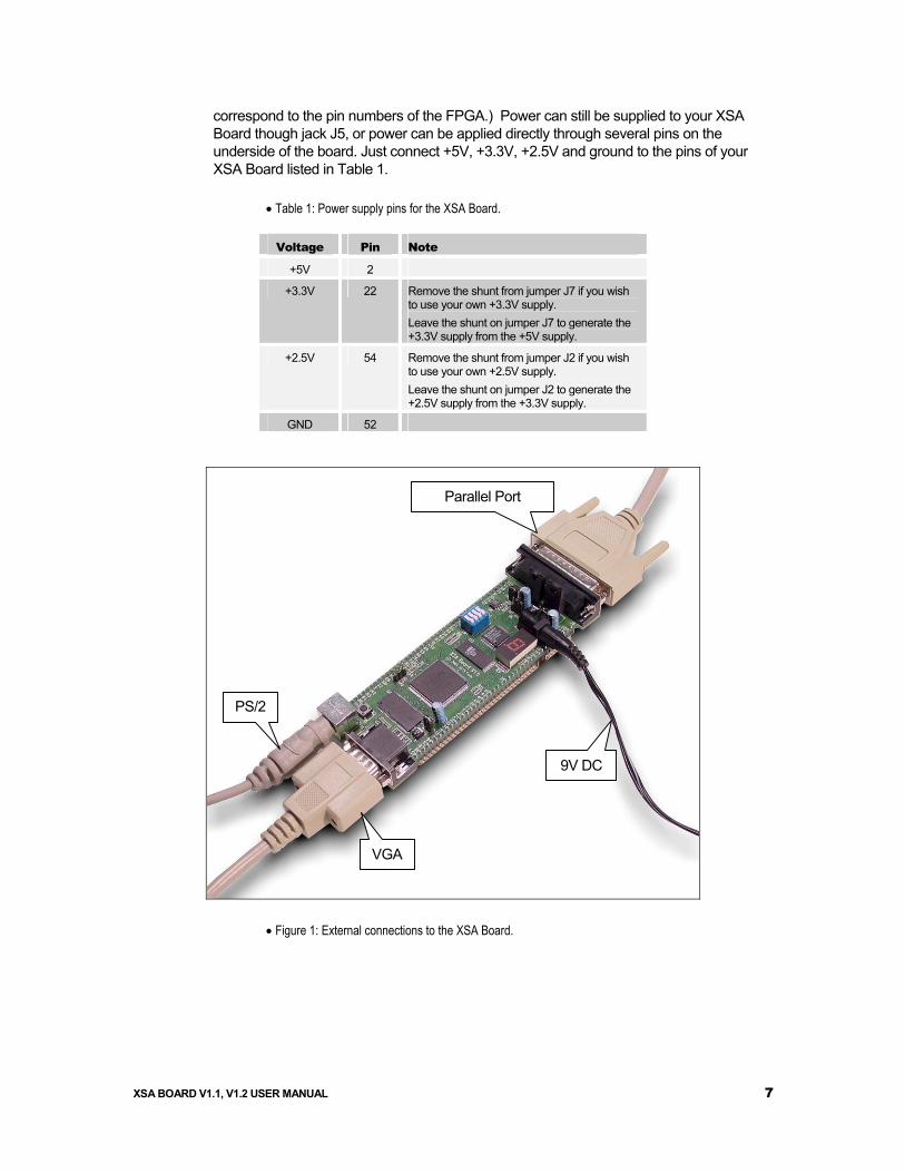
correspond to the pin numbers of the FPGA.) Power can still be supplied to your XSA Board though jack J5, or power can be applied directly through several pins on the underside of the board. Just connect +5V, +3.3V, +2.5V and ground to the pins of your XSA Board listed in Table 1.
• Table 1: Power supply pins for the XSA Board.
Voltage Pin Note
+5V 2
+3.3V 22 Remove the shunt from jumper J7 if you wish to use your own +3.3V supply. Leave the shunt on jumper J7 to generate the +3.3V supply from the +5V supply.
+2.5V 54 Remove the shunt from jumper J2 if you wish to use your own +2.5V supply. Leave the shunt on jumper J2 to generate the +2.5V supply from the +3.3V supply.
GND 52
Parallel Port
PS/2
9V DC
VGA
• Figure 1: External connections to the XSA Board.
XSA BOARD V1.1, V1.2 USER MANUAL 7
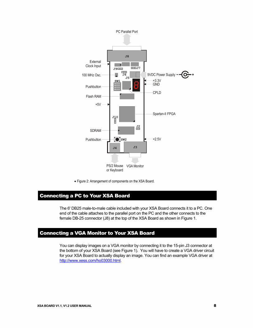
J6J5
J9
J2
J10
J3J4
SW2
J8
J7
Spartan-II FPGA
CPLDFlash RAM
SDRAM
Pushbutton
Pushbutton
100 MHz Osc.
ExternalClock Input
+5V
+3.3V
+2.5V
GND
VGA Monitor
PC Parallel Port
9VDC Power Supply
PS/2 Mouseor Keyboard
U10
U15SW1
• Figure 2: Arrangement of components on the XSA Board.
Connecting a PC to Your XSA Board
The 6' DB25 male-to-male cable included with your XSA Board connects it to a PC. One end of the cable attaches to the parallel port on the PC and the other connects to the female DB-25 connector (J8) at the top of the XSA Board as shown in Figure 1.
Connecting a VGA Monitor to Your XSA Board
You can display images on a VGA monitor by connecting it to the 15-pin J3 connector at the bottom of your XSA Board (see Figure 1). You will have to create a VGA driver circuit for your XSA Board to actually display an image. You can find an example VGA driver at http://www.xess.com/ho03000.html.
XSA BOARD V1.1, V1.2 USER MANUAL 8
Connecting a Mouse or Keyboard to Your XSA Board
You can accept inputs from a keyboard or mouse by connecting it to the J4 PS/2 connector at the bottom of your XSA Board (see Figure 1). You can find an example keyboard driver at http://www.xess.com/ho03000.html.
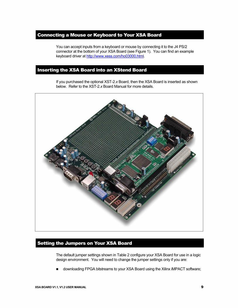
Inserting the XSA Board into an XStend Board
If you purchased the optional XST-2.x Board, then the XSA Board is inserted as shown below. Refer to the XST-2.x Board Manual for more details.
Setting the Jumpers on Your XSA Board
The default jumper settings shown in Table 2 configure your XSA Board for use in a logic design environment. You will need to change the jumper settings only if you are:
downloading FPGA bitstreams to your XSA Board using the Xilinx iMPACT software;
XSA BOARD V1.1, V1.2 USER MANUAL 9
reprogramming the clock frequency on your XSA Board (see page 11);
changing the power sources for the XSA supply voltages.
• Table 2: Jumper settings for XSA Boards.
Jumper Setting Purpose
On (default)
A shunt should be installed if the +2.5V supply voltage is derived from the +3.3V supply. J2
Off The shunt should be removed if the +2.5V supply voltage is applied from an external source through pin 22 of the XSA Board (labeled “+2.5V” at the lower right-hand corner of the board).
1-2 (set) The shunt should be installed on pins 1 and 2 (set) when setting the frequency of the programmable oscillator.
J6
2-3 (osc) (default)
The shunt should be installed on pins 2 and 3 (osc) during normal operations when the programmable oscillator is generating a clock signal.
1-2 (default)
The shunt should be installed on pins 1 and 2 if the +3.3V supply voltage is derived from the +5V supply.
J7
2-3 The shunt should be installed on pins 2 and 3 if the +3.3V supply voltage is derived from the 9VDC supply applied through jack J5.
1-2 (xi) The shunt should be installed on pins 1 and 2 (xi) if the XSA Board is to be downloaded using the Xilinx iMPACT software.
J9
2-3 (xs) (default)
The shunt should be installed on pins 2 and 3 (xs) if the XSA Board is to be downloaded using the XESS GXSLOAD software.
J10 N/A This is a header that provides access to the +5V and GND references on the board. No shunt should be placed on this header.
Testing Your XSA Board
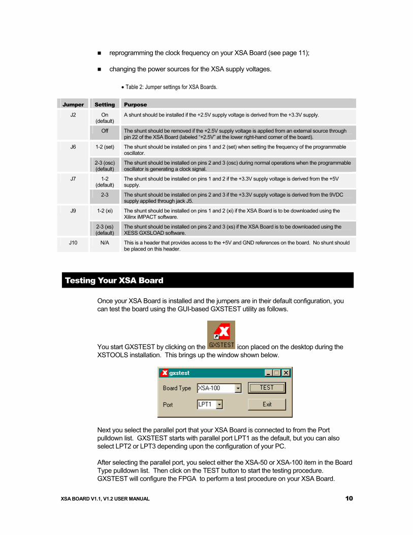
Once your XSA Board is installed and the jumpers are in their default configuration, you can test the board using the GUI-based GXSTEST utility as follows.
You start GXSTEST by clicking on the icon placed on the desktop during the XSTOOLS installation. This brings up the window shown below.
Next you select the parallel port that your XSA Board is connected to from the Port pulldown list. GXSTEST starts with parallel port LPT1 as the default, but you can also select LPT2 or LPT3 depending upon the configuration of your PC.
After selecting the parallel port, you select either the XSA-50 or XSA-100 item in the Board Type pulldown list. Then click on the TEST button to start the testing procedure. GXSTEST will configure the FPGA to perform a test procedure on your XSA Board.
XSA BOARD V1.1, V1.2 USER MANUAL 10
Within thirty seconds you will see a O displayed on the LED digit if the test completes successfully. Otherwise an E will be displayed if the test fails. A status window will also appear on your PC screen informing you of the success or failure of the test.
If your XSA Board fails the test, you will be shown a checklist of common causes for failure. If none of these causes applies to your situation, then test the XSA Board using another PC. In our experience, 99.9% of all problems are due to the parallel port. If you cannot get your board to pass the test even after taking these steps, then contact XESS Corp for further assistance.
As a result of testing the XSA Board, the CPLD is programmed with the standard parallel port interface found in the dwnldpar.svf bitstream file located within the XSTOOLS\XSA folder. This is the standard interface that should be loaded into the CPLD when you want to use it with the GXSLOAD utility.
Setting the XSA Board Clock Oscillator Frequency
The XSA Board has a 100 MHz programmable oscillator (a Dallas Semiconductor DS1075Z-100). The 100 MHz master frequency can be divided by factors of 1, 2, ... up to 2052 to get clock frequencies of 100 MHz, 50 MHz, ... down to 48.7 KHz, respectively. The divided frequency is sent to the rest of the XSA Board circuitry as a clock signal.
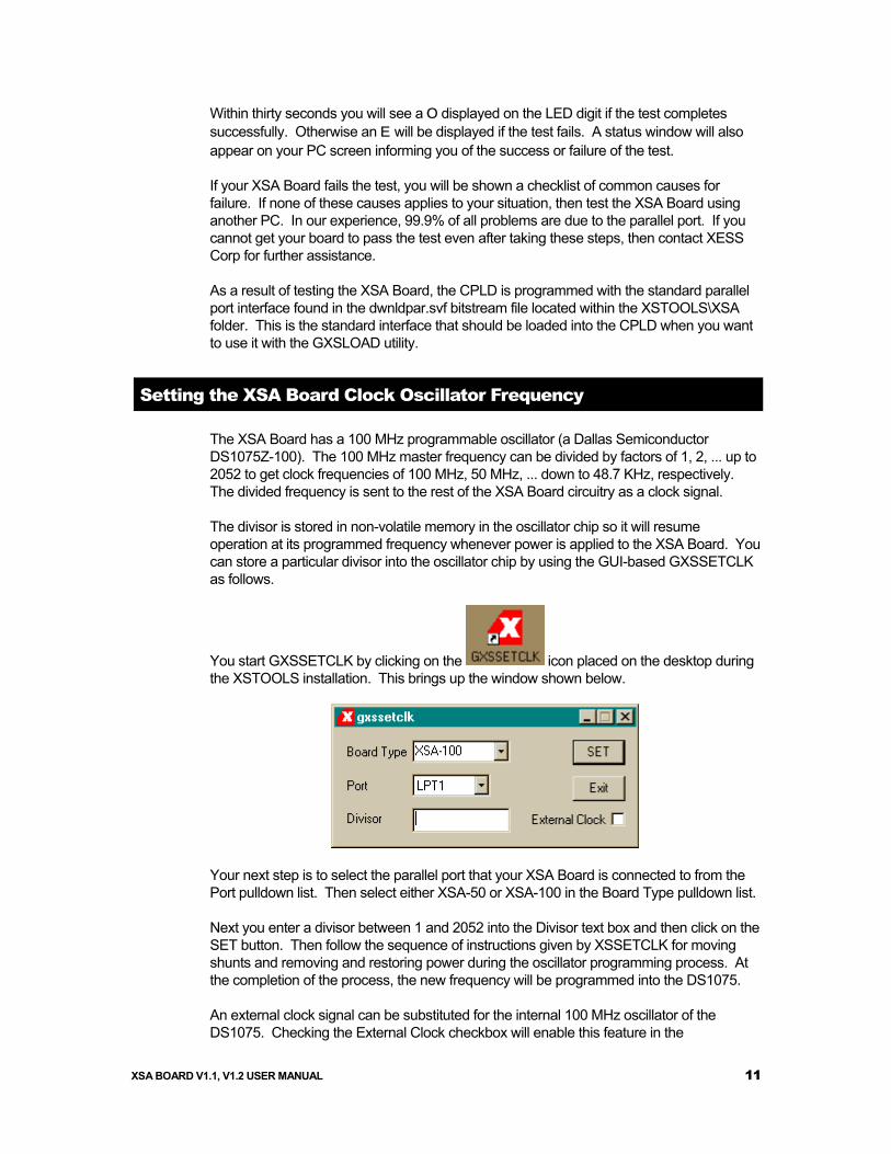
The divisor is stored in non-volatile memory in the oscillator chip so it will resume operation at its programmed frequency whenever power is applied to the XSA Board. You can store a particular divisor into the oscillator chip by using the GUI-based GXSSETCLK as follows.
You start GXSSETCLK by clicking on the icon placed on the desktop during the XSTOOLS installation. This brings up the window shown below.
Your next step is to select the parallel port that your XSA Board is connected to from the Port pulldown list. Then select either XSA-50 or XSA-100 in the Board Type pulldown list.
Next you enter a divisor between 1 and 2052 into the Divisor text box and then click on the SET button. Then follow the sequence of instructions given by XSSETCLK for moving shunts and removing and restoring power during the oscillator programming process. At the completion of the process, the new frequency will be programmed into the DS1075.
An external clock signal can be substituted for the internal 100 MHz oscillator of the DS1075. Checking the External Clock checkbox will enable this feature in the
XSA BOARD V1.1, V1.2 USER MANUAL 11
programmable oscillator chip. If this option is selected, you are then responsible for providing the external clock to the XSA Board through pin 64 (labeled “CLK” at the upper left-hand corner of the board).
XSA BOARD V1.1, V1.2 USER MANUAL 12
3 Programming
This section will show you how to download a logic designs into the FPGA and CPLD of your XSA Board and how to download and upload data to and from the SDRAM and Flash devices on the board.
Downloading Designs into the FPGA and CPLD of Your XSA Board
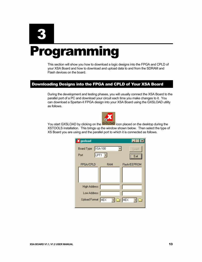
During the development and testing phases, you will usually connect the XSA Board to the parallel port of a PC and download your circuit each time you make changes to it. You can download a Spartan-II FPGA design into your XSA Board using the GXSLOAD utility as follows.
You start GXSLOAD by clicking on the icon placed on the desktop during the XSTOOLS installation. This brings up the window shown below. Then select the type of XS Board you are using and the parallel port to which it is connected as follows.
XSA BOARD V1.1, V1.2 USER MANUAL 13
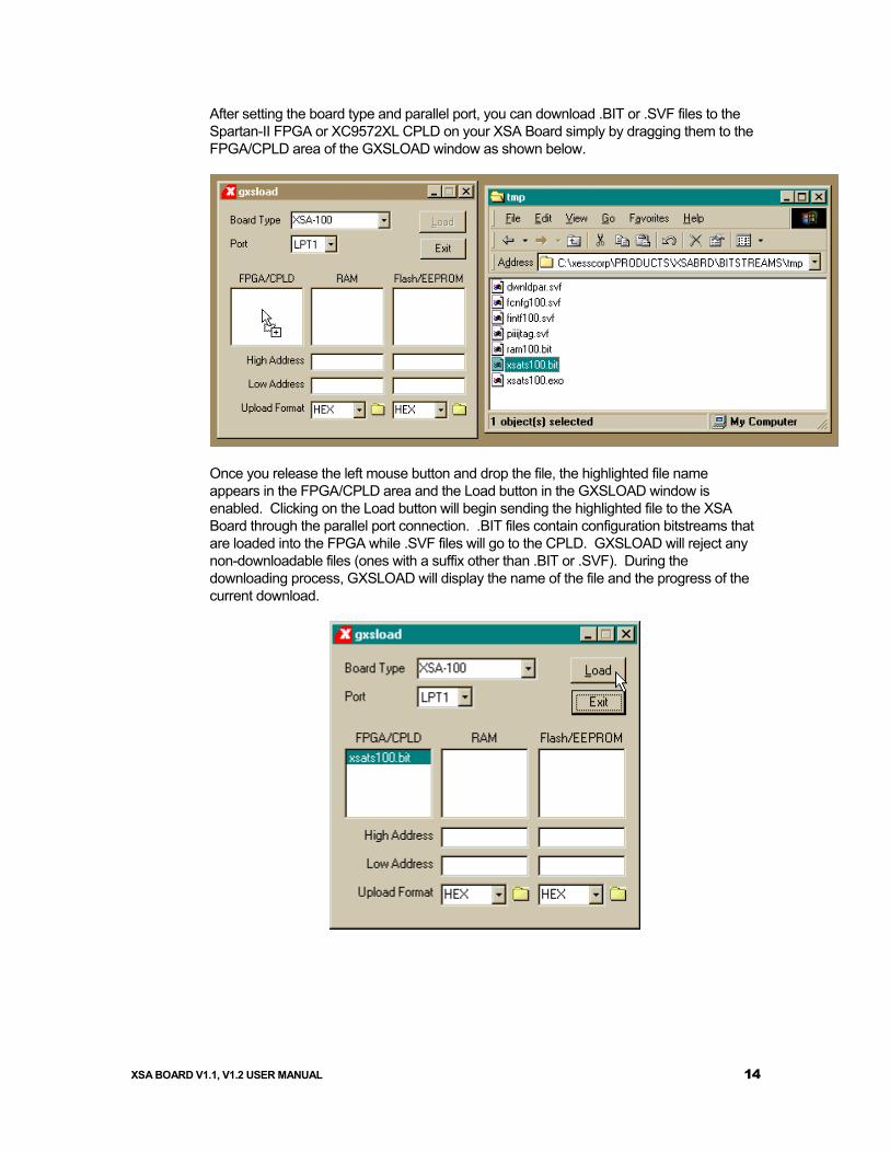
After setting the board type and parallel port, you can download .BIT or .SVF files to the Spartan-II FPGA or XC9572XL CPLD on your XSA Board simply by dragging them to the FPGA/CPLD area of the GXSLOAD window as shown below.
Once you release the left mouse button and drop the file, the highlighted file name appears in the FPGA/CPLD area and the Load button in the GXSLOAD window is enabled. Clicking on the Load button will begin sending the highlighted file to the XSA Board through the parallel port connection. .BIT files contain configuration bitstreams that are loaded into the FPGA while .SVF files will go to the CPLD. GXSLOAD will reject any non-downloadable files (ones with a suffix other than .BIT or .SVF). During the downloading process, GXSLOAD will display the name of the file and the progress of the current download.
XSA BOARD V1.1, V1.2 USER MANUAL 14
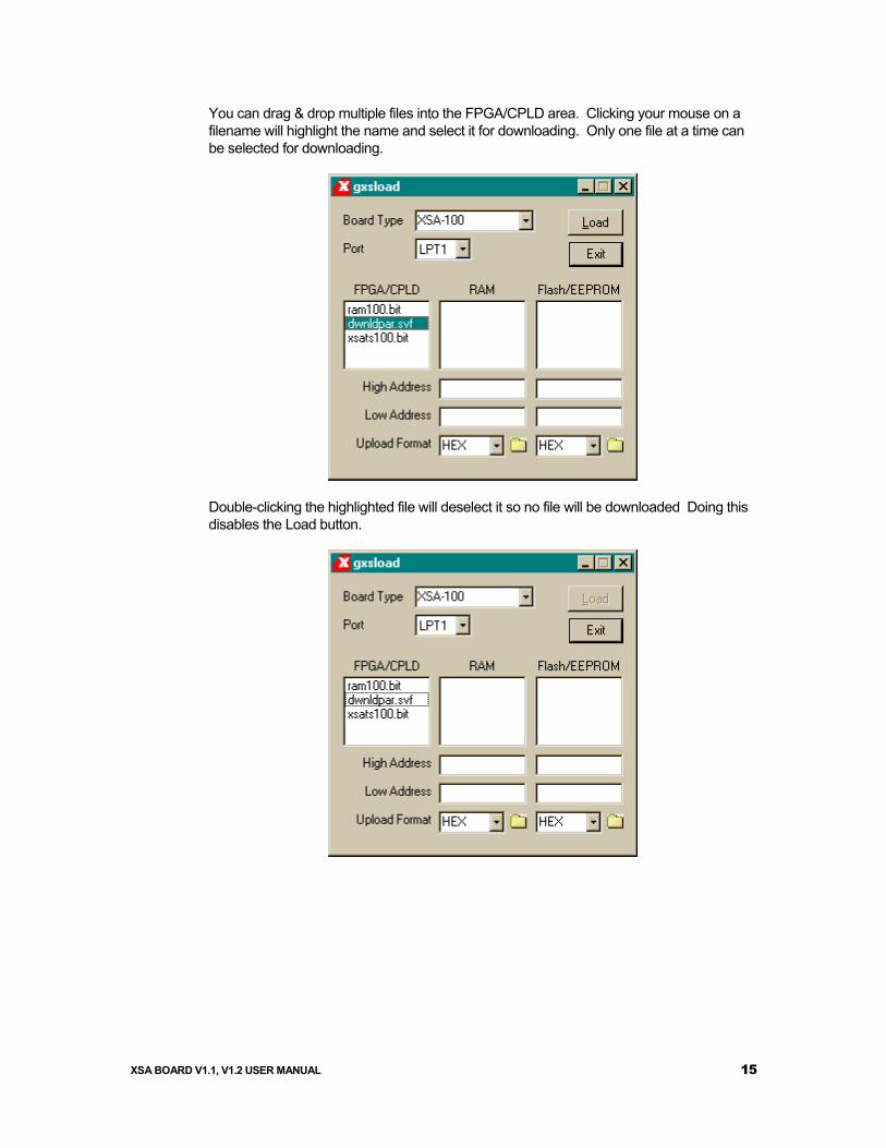
You can drag & drop multiple files into the FPGA/CPLD area. Clicking your mouse on a filename will highlight the name and select it for downloading. Only one file at a time can be selected for downloading.
Double-clicking the highlighted file will deselect it so no file will be downloaded Doing this disables the Load button.
XSA BOARD V1.1, V1.2 USER MANUAL 15
Storing Non-Volatile Designs in Your XSA Board
The Spartan-II FPGA on the XSA Board stores its configuration in an on-chip SRAM which is erased whenever power is removed. Once your design is finished, you may want to store the bitstream in the 256-KByte Flash device on the XSA Board which configures the FPGA for operation as soon as power is applied.
Before downloading to the Flash, the FPGA .BIT file must be converted into a .EXO or .MCS format using one of the following commands:
promgen –u 0 file.bit –p exo –s 256
promgen –u 0 file.bit –p mcs –s 256
In the commands shown above, the bitstream in the file.bit file is transformed into an .EXO or .MCS file format starting at address zero and proceeding upward until an upper limit of 256 KBytes is reached.
Before attempting to program the Flash, you must place all four DIP switches into the OFF position!
After the .EXO or .MCS file is generated, it is loaded into the Flash device by dragging it into the Flash/EEPROM area and clicking on the Load button. This activates the following sequence of steps:
1. The entire Flash device is erased.
2. The CPLD on the XSA Board is reprogrammed to create an interface between the Flash device and the PC parallel port. (This interface is stored in the fintf.svf bitstream file located within the XSTOOLS\XSA folder.)
3. The contents of the .EXO or .MCS file are downloaded into the Flash through the parallel port.
4. The CPLD is reprogrammed to create a circuit that configures the FPGA with the contents of the Flash when power is applied to the XSA Board. (This configuration loader is stored in the fcnfg.svf bitstream file located within the XSTOOLS\XSA folder.)
Multiple files can be stored in the Flash device just by dragging them into the Flash/EEPROM area, highlighting the files to be downloaded and clicking the Load button. (Note that anything previously stored in the Flash will be erased by each new download.) This is useful if you need to store information in the Flash in addition to the FPGA bitstream. Files are selected and de-selected for downloading just by clicking on their names in the Flash/EEPROM area. The address ranges of the data in each file should not overlap or this will corrupt the data stored in the Flash device!
XSA BOARD V1.1, V1.2 USER MANUAL 16
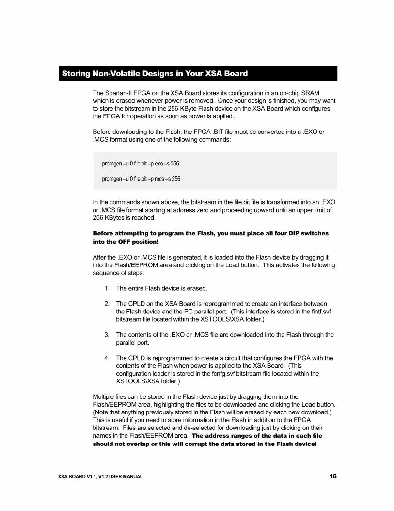
You can also examine the contents of the Flash device by uploading it to the PC. To upload data from an address range in the Flash, type the upper and lower bounds of the range into the High Address and Low Address fields below the Flash/EEPROM area, and select the format in which you would like to store the data using the Upload Format pulldown list. Then click on the file icon and drag & drop it into any folder. This activates the following sequence of steps:
1. The CPLD on the XSA Board is reprogrammed to create an interface between the Flash device and the PC parallel port.
2. The Flash data between the high and low addresses (inclusive) is uploaded through the parallel port.
3. The uploaded data is stored in a file named FLSHUPLD with an extension that reflects the file format.
The uploaded data can be stored in the following formats:
MCS: Intel hexadecimal file format. This is the same format generated by the promgen utility with the –p mcs option.
HEX: Identical to MCS format.
EXO-16: Motorola S-record format with 16-bit addresses (suitable for 64 KByte uploads only).
EXO-24: Motorola S-record format with 24-bit addresses. This is the same format generated by the promgen utility with the –p exo option.
EXO-32: Motorola S-record format with 32-bit addresses.
XESS-16: XESS hexadecimal format with 16-bit addresses. (This is a simplified file format that does not use checksums.)
XESS-24: XESS hexadecimal format with 24-bit addresses.
XSA BOARD V1.1, V1.2 USER MANUAL 17
XESS-32: XESS hexadecimal format with 32-bit addresses.
After the data is uploaded from the Flash, the CPLD on the XSA Board is left with the Flash interface programmed into it. You will need to reprogram the CPLD with either the parallel port or Flash configuration circuit before the board will function again. The CPLD configuration bitstreams are stored in the following files:
XSTOOLS\XSA\dwnldpar.svf: Drag & drop this file into the FPGA/CPLD area and click on the Load button to put the XSA in a mode where it will configure the FPGA through the parallel port.
XSTOOLS\XSA\ fcnfg.svf: Drag & drop this file into the FPGA/CPLD area and click on the Load button to put the XSA in a mode where it will configure the FPGA with the contents of the Flash device upon power-up.
Downloading and Uploading Data to the SDRAM in Your XSA Board
The XSA-100 Board contains a 16-MByte synchronous DRAM (8M x 16 SDRAM) whose contents can be downloaded and uploaded by GXSLOAD. (The XSA-50 has an 8-MByte SDRAM organized as 4M x 16.) This is useful for initializing the SDRAM with data for use by the FPGA and then reading the SDRAM contents after the FPGA has operated upon it. The SDRAM is loaded with data by dragging & dropping one or more .EXO, .MCS, .HEX, and/or .XES files into the RAM area of the GXSLOAD window and then clicking on the Load button. This activates the following sequence of steps:
1. The Spartan-II FPGA on the XSA Board is reprogrammed to create an interface between the RAM device and the PC parallel port. (This interface is stored in the ram100.bit or ram50.bit bitstream file located within the XSTOOLS\XSA folder. The CPLD must have previously been loaded with the dwnldpar.svf file found in the same folder.)
2. The contents of the .EXO, .MCS, .HEX or .XES files are downloaded into the SDRAM through the parallel port. The data in the files will overwrite each other if their address ranges overlap.
3. If any file is highlighted in the FPGA/CPLD area, then this bitstream is loaded into the FPGA or CPLD on the XSA Board. Otherwise the FPGA remains configured as an interface between the PC and the SDRAM.
You can also examine the contents of the SDRAM device by uploading it to the PC. To upload data from an address range in the SDRAM, type the upper and lower bounds of the range into the High Address and Low Address fields below the RAM area, and select the format in which you would like to store the data using the Upload Format pulldown list. Then click on the file icon and drag & drop it into any folder. This activates the following sequence of steps:
1. The Spartan-II FPGA on the XSA Board is reprogrammed to create an interface between the RAM device and the PC parallel port. (This interface is stored in the ram100.bit or ram50.bit bitstream file located within the XSTOOLS\XSA folder.)
2. The SDRAM data between the high and low addresses (inclusive) is uploaded through the parallel port.
XSA BOARD V1.1, V1.2 USER MANUAL 18
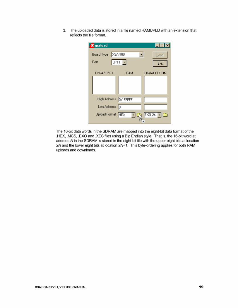
3. The uploaded data is stored in a file named RAMUPLD with an extension that reflects the file format.
The 16-bit data words in the SDRAM are mapped into the eight-bit data format of the .HEX, .MCS, .EXO and .XES files using a Big Endian style. That is, the 16-bit word at address N in the SDRAM is stored in the eight-bit file with the upper eight bits at location 2N and the lower eight bits at location 2N+1. This byte-ordering applies for both RAM uploads and downloads.
XSA BOARD V1.1, V1.2 USER MANUAL 19
4 Programmer's Models
This section describes the various sections of the XSA Board and shows how the I/O of the FPGA and CPLD are connected to the rest of the circuitry. The schematics which follow are less detailed so as to simplify the descriptions. Please refer to the complete schematics at the end of this document if you need more details.
XSA Board Organization
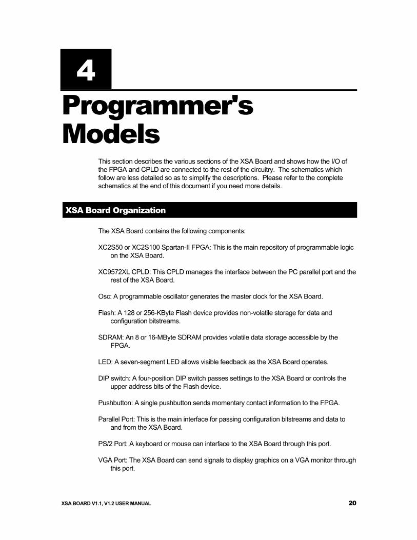
The XSA Board contains the following components:
XC2S50 or XC2S100 Spartan-II FPGA: This is the main repository of programmable logic on the XSA Board.
XC9572XL CPLD: This CPLD manages the interface between the PC parallel port and the rest of the XSA Board.
Osc: A programmable oscillator generates the master clock for the XSA Board.
Flash: A 128 or 256-KByte Flash device provides non-volatile storage for data and configuration bitstreams.
SDRAM: An 8 or 16-MByte SDRAM provides volatile data storage accessible by the FPGA.
LED: A seven-segment LED allows visible feedback as the XSA Board operates.
DIP switch: A four-position DIP switch passes settings to the XSA Board or controls the upper address bits of the Flash device.
Pushbutton: A single pushbutton sends momentary contact information to the FPGA.
Parallel Port: This is the main interface for passing configuration bitstreams and data to and from the XSA Board.
PS/2 Port: A keyboard or mouse can interface to the XSA Board through this port.
VGA Port: The XSA Board can send signals to display graphics on a VGA monitor through this port.
XSA BOARD V1.1, V1.2 USER MANUAL 20
Prototyping Header: Many of the FPGA I/O pins are connected to the 84 pins on the bottom of the XSA Board that are meant to mate with solderless breadboards.
A17 - A0
D7 - D0
/HSYNC
PSCLK
CKE
/VSYNC
PSDATA
CLK
BLUE1 - BLUE0
GREEN1 - GREEN0
/CE
/OE
/WE
/RES
ET
A17-
A0
D7-D
0
8
TCKTMSTDI
TDO
GCLK
2 - PPD03 - PPD14 - PPD25 - PPD36 - PPD47 - PPD58 - PPD69 - PPD7
17 - PPC316 - PPC214 - PPC1
1 - PPC0
11 - PPS7
10 - PPS6
15 - PPS313 - PPS412 - PPS5
XC9572XL
OSC
FLASH
PS/2 Port
Parallel Port
SDRAM
VGA Connector
RED1 - RED0
D15 - D0
BA1 - BA0, A12 - A0
RAS, CAS, /CS, /WE
DQMLDQMH
D7-D0
CCLK/PROGRAM
BSY/DOUT/WR/CS
/INITM0M1M2
DONETCKTMSTDITDOGCLK
GCLK
XC2S100
• Figure 3: XSA Board programmer’s model.
Programmable logic: Spartan-II FPGA and XC9572XL CPLD
The XSA Board contains two programmable logic chips:
A 50-Kgate XC2S50 or 100-Kgate Xilinx XC2S100 Spartan-II FPGA in a 144-pin PQFP package. The FPGA is the main repository of programmable logic on the XSA Board.
A Xilinx XC9572XL CPLD is used to manage the configuration of the FPGA via the parallel port. The CPLD also controls the programming of the Flash RAM on the XSA Board.
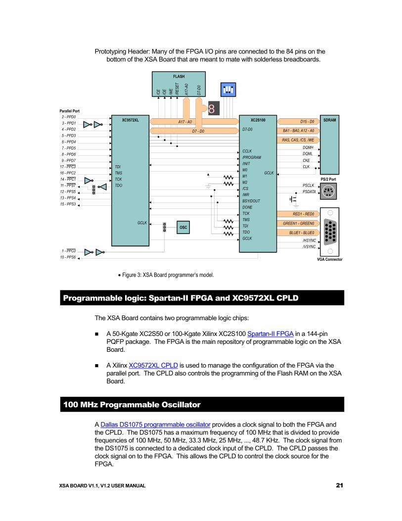
100 MHz Programmable Oscillator
A Dallas DS1075 programmable oscillator provides a clock signal to both the FPGA and the CPLD. The DS1075 has a maximum frequency of 100 MHz that is divided to provide frequencies of 100 MHz, 50 MHz, 33.3 MHz, 25 MHz, ..., 48.7 KHz. The clock signal from the DS1075 is connected to a dedicated clock input of the CPLD. The CPLD passes the clock signal on to the FPGA. This allows the CPLD to control the clock source for the FPGA.
XSA BOARD V1.1, V1.2 USER MANUAL 21
To set the divisor value, the DS1075 must be placed in its programming mode. This is done by pulling the clock output to +5V on power-up with a shunt across pins 1 and 2 of jumper J6. Then programming commands to set the divisor are sent to the DS1075 through control pin C0 of the parallel port. The divisor is stored in EEPROM in the DS1075 so it will be retained even when power is removed from the XSA Board.
The shunt on jumper J6 must be across pins 2 and 3 to make the oscillator output a clock signal upon power-up. The clock signal enters a dedicated clock input of the CPLD. Then the CPLD can output a clock signal to a dedicated clock input of the FPGA.
To get a precise frequency value or to sync the XSA circuitry with an external system, you can insert an external clock signal of up to 50 MHz through pin 64 of the prototyping header. This external clock takes the place of the internal 100 MHz clock source in the DS1075 oscillator. You must use the GXSSETCLK software utility to enable the external clock input of the DS1075.
Clock signals can also be directly applied to two of the dedicated clock inputs of the FPGA through the pins of the prototyping header.
Spartan-IIFPGA
88
15
18
2
3
1
XC9572XLCPLD
17
J6
PP-C0
Pin 64
Pin 31
Pin 1DS1075
100 MHzProg. Osc.
+5V
42
XSA BOARD V1.1, V1.2 USER MANUAL 22
Synchronous DRAM
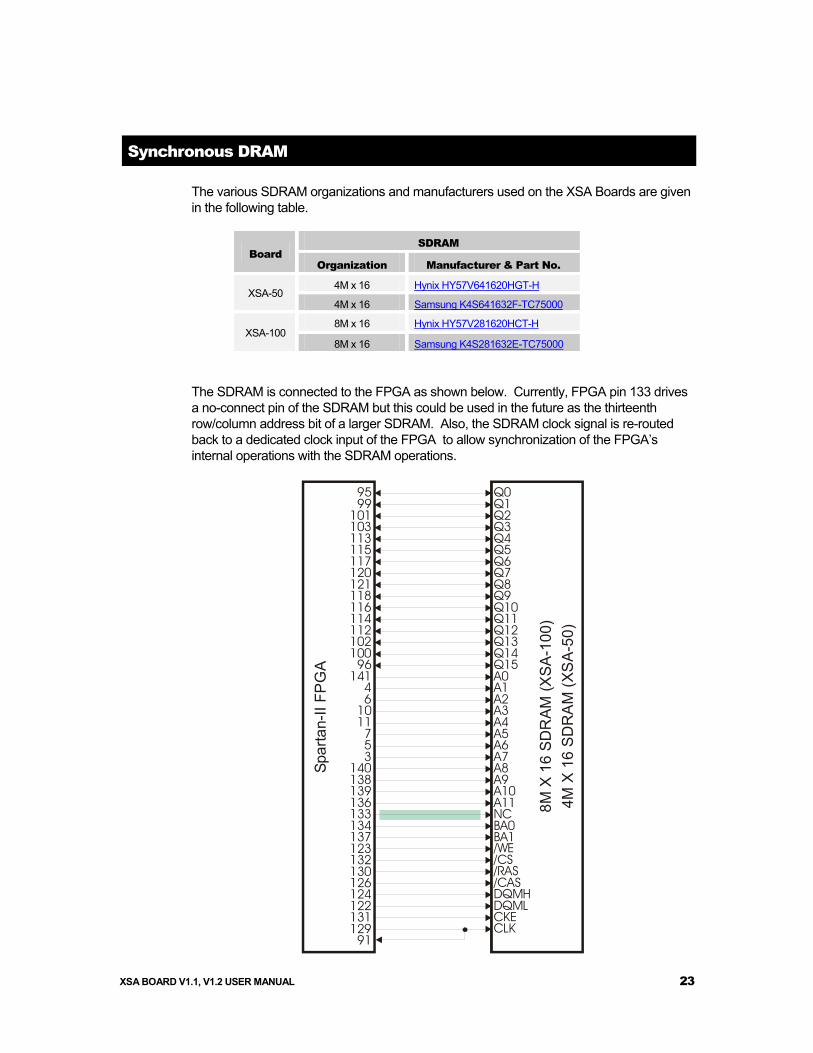
The various SDRAM organizations and manufacturers used on the XSA Boards are given in the following table.
SDRAM Board
Organization Manufacturer & Part No.
4M x 16 Hynix HY57V641620HGT-H XSA-50
4M x 16 Samsung K4S641632F-TC75000
8M x 16 Hynix HY57V281620HCT-H XSA-100
8M x 16 Samsung K4S281632E-TC75000
The SDRAM is connected to the FPGA as shown below. Currently, FPGA pin 133 drives a no-connect pin of the SDRAM but this could be used in the future as the thirteenth row/column address bit of a larger SDRAM. Also, the SDRAM clock signal is re-routed back to a dedicated clock input of the FPGA to allow synchronization of the FPGA’s internal operations with the SDRAM operations.
8M X
16
SDR
AM (X
SA-1
00)
4M X
16
SDR
AM
(XS
A-50
)
Spar
tan-
II FP
GA
95 Q0
3 A7
133 NC136 A11139 A10138 A9140 A8
5 A67 A511 A410 A36 A24 A1
141 A096 Q15
99 Q1
100 Q14102 Q13112 Q12114 Q11116 Q10118 Q9121 Q8120 Q7117 Q6115 Q5113 Q4103 Q3101 Q2
134
124
129131122
137
126130132123
91
BA0
/CAS
CKEDQMLDQMH
BA1
/RAS/CS/WE
CLK
XSA BOARD V1.1, V1.2 USER MANUAL 23
Flash RAM
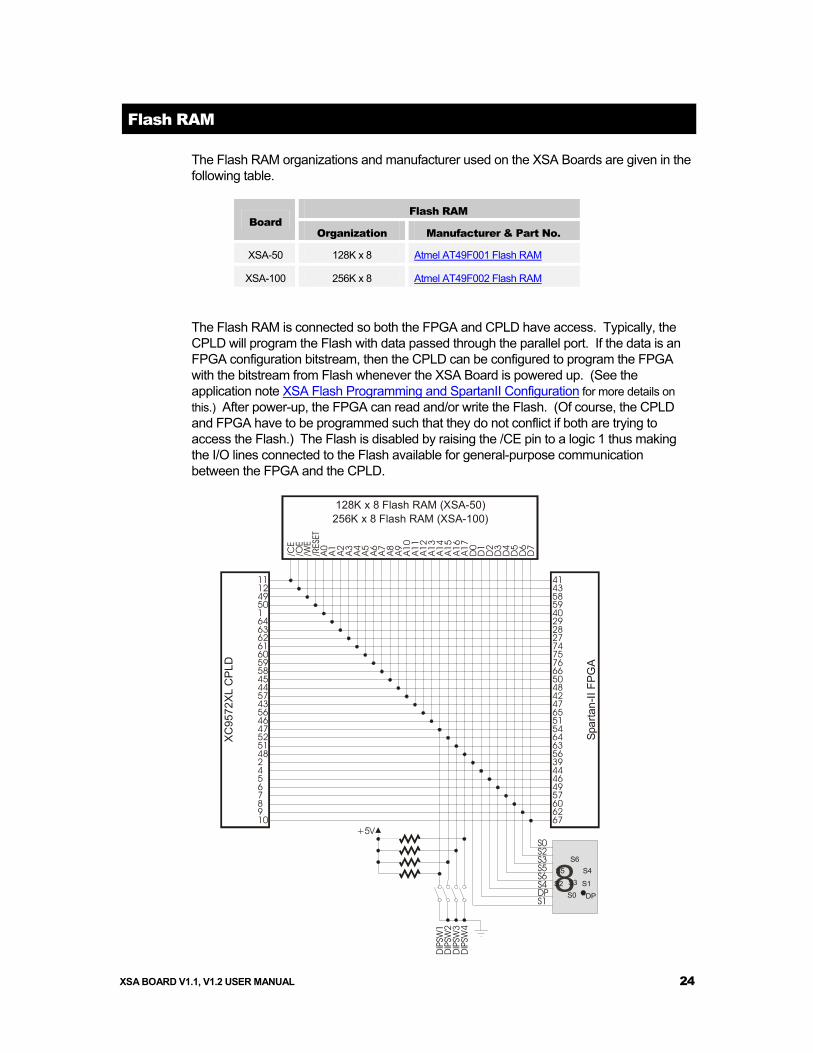
The Flash RAM organizations and manufacturer used on the XSA Boards are given in the following table.
Flash RAM Board
Organization Manufacturer & Part No.
XSA-50 128K x 8 Atmel AT49F001 Flash RAM
XSA-100 256K x 8 Atmel AT49F002 Flash RAM
The Flash RAM is connected so both the FPGA and CPLD have access. Typically, the CPLD will program the Flash with data passed through the parallel port. If the data is an FPGA configuration bitstream, then the CPLD can be configured to program the FPGA with the bitstream from Flash whenever the XSA Board is powered up. (See the application note XSA Flash Programming and SpartanII Configuration for more details on this.) After power-up, the FPGA can read and/or write the Flash. (Of course, the CPLD and FPGA have to be programmed such that they do not conflict if both are trying to access the Flash.) The Flash is disabled by raising the /CE pin to a logic 1 thus making the I/O lines connected to the Flash available for general-purpose communication between the FPGA and the CPLD.
256K x 8 Flash RAM (XSA-100)128K x 8 Flash RAM (XSA-50)
XC95
72XL
CPL
D
Spar
tan-
II FP
GA
A0/CE
11 41
4 4
S2
9 6
DP
8 6
S4
7 5
S6
6 4
S5
5 4
S3
2 3
S0+5V
48 5651 6352 6447 5446 5156 6543 47
12 43
57 4244 4845 5058 6659 7660 7561 7462 2763 2864 291 450 5949 58
10 67
S1
D0
A2/WE
D2
A3/RESET
D3
A4 D4
A5 D5
A6 D6
A7 D7
A8 A9A1/OE
D1
A10
A11
A12
A13
A14
A15
A16
A17
4
20796
9
0
8S1
DP
S2 S3S4S5
S6
S0
DIPSW
4DIPSW
3DIPSW
2DIPSW
1
XSA BOARD V1.1, V1.2 USER MANUAL 24
Seven-Segment LED
The XSA Board has a 7-segment LED digit for use by the FPGA or the CPLD. The segments of this LED are active-high meaning that a segment will glow when a logic-high is applied to it.
The LED shares the same pins as the eight bits of the Flash RAM data bus.
Four-Position DIP Switch
The XSA Board has a bank of four DIP switches accessible from the CPLD and FPGA. When closed or ON, each switch pulls the connected pin of the FPGA and CPLD to ground. Otherwise, the pin is pulled high through a resistor when the switch is open or OFF.
When not being used, the DIP switches should be left in the open or OFF configuration so the pins of the FPGA and CPLD are not tied to ground and can freely move between logic low and high levels.
The DIP switches also share the same pins as the uppermost four bits of the Flash RAM address bus. If the Flash RAM is programmed with several FPGA bitstreams, then the DIP switches can be used to select a particular bitstreams which will be loaded into the FPGA by the CPLD on power-up. However, this feature is not currently supported by the CPLD configuration that loads the FPGA from the Flash RAM (XSTOOLS\XSA\fcnfg.svf).
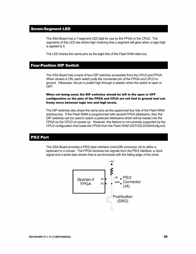
PS/2 Port
The XSA Board provides a PS/2-style interface (mini-DIN connector J4) to either a keyboard or a mouse. The FPGA receives two signals from the PS/2 interface: a clock signal and a serial data stream that is synchronized with the falling edge of the clock.
Spartan-IIFPGA data
94
93
clk PS/2Connector(J4)
+5V
Pushbutton(SW2)
XSA BOARD V1.1, V1.2 USER MANUAL 25
Pushbutton
The XSA Board has a single pushbutton that shares the FPGA pin connected to the data line of the PS/2 port. The pushbutton applies a low level to the FPGA pin when pressed and a resistor pulls the pin to a high level when the pushbutton is not pressed.
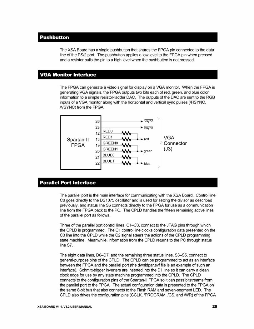
VGA Monitor Interface
The FPGA can generate a video signal for display on a VGA monitor. When the FPGA is generating VGA signals, the FPGA outputs two bits each of red, green, and blue color information to a simple resistor-ladder DAC. The outputs of the DAC are sent to the RGB inputs of a VGA monitor along with the horizontal and vertical sync pulses (/HSYNC, /VSYNC) from the FPGA.
Spartan-IIFPGA
red
2623
2120191312 RED0
RED1
BLUE0GREEN1GREEN0
BLUE122
hsync
vsync
green
blue
VGAConnector(J3)
Parallel Port Interface
The parallel port is the main interface for communicating with the XSA Board. Control line C0 goes directly to the DS1075 oscillator and is used for setting the divisor as described previously, and status line S6 connects directly to the FPGA for use as a communication line from the FPGA back to the PC. The CPLD handles the fifteen remaining active lines of the parallel port as follows.
Three of the parallel port control lines, C1–C3, connect to the JTAG pins through which the CPLD is programmed. The C1 control line clocks configuration data presented on the C3 line into the CPLD while the C2 signal steers the actions of the CPLD programming state machine. Meanwhile, information from the CPLD returns to the PC through status line S7.
The eight data lines, D0–D7, and the remaining three status lines, S3–S5, connect to general-purpose pins of the CPLD. The CPLD can be programmed to act as an interface between the FPGA and the parallel port (the dwnldpar.svf file is an example of such an interface). Schmitt-trigger inverters are inserted into the D1 line so it can carry a clean clock edge for use by any state machine programmed into the CPLD. The CPLD connects to the configuration pins of the Spartan-II FPGA so it can pass bitstreams from the parallel port to the FPGA. The actual configuration data is presented to the FPGA on the same 8-bit bus that also connects to the Flash RAM and seven-segment LED. The CPLD also drives the configuration pins (CCLK, /PROGRAM, /CS, and /WR) of the FPGA
XSA BOARD V1.1, V1.2 USER MANUAL 26
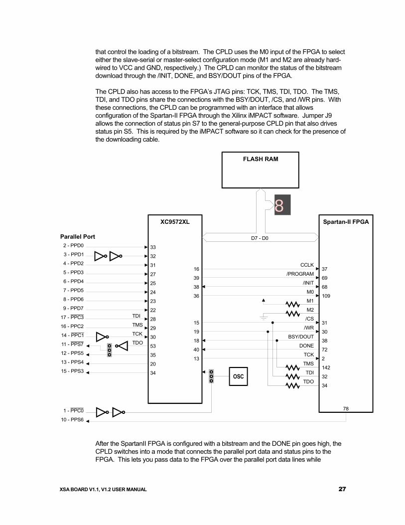
that control the loading of a bitstream. The CPLD uses the M0 input of the FPGA to select either the slave-serial or master-select configuration mode (M1 and M2 are already hard-wired to VCC and GND, respectively.) The CPLD can monitor the status of the bitstream download through the /INIT, DONE, and BSY/DOUT pins of the FPGA.
The CPLD also has access to the FPGA’s JTAG pins: TCK, TMS, TDI, TDO. The TMS, TDI, and TDO pins share the connections with the BSY/DOUT, /CS, and /WR pins. With these connections, the CPLD can be programmed with an interface that allows configuration of the Spartan-II FPGA through the Xilinx iMPACT software. Jumper J9 allows the connection of status pin S7 to the general-purpose CPLD pin that also drives status pin S5. This is required by the iMPACT software so it can check for the presence of the downloading cable.
D7 - D0
8
TCK
TMS
TDI
TDO
2 - PPD0
3 - PPD1
4 - PPD2
5 - PPD3
6 - PPD4
7 - PPD5
8 - PPD6
9 - PPD7
17 - PPC3
16 - PPC2
14 - PPC1
1 - PPC0
11 - PPS7
10 - PPS6
15 - PPS3
13 - PPS4
12 - PPS5
XC9572XL
OSC
FLASH RAM
Parallel Port
CCLK37
33
28
20
35
53
30
29
32
22
23
24
25
27
31
34
16
15
40
18
19
39
36
38
13
38
32
142
2
72
30
69
31
109
68
34
78
/PROGRAM
BSY/DOUT
/WR
/CS
/INIT
M0
M1
M2
DONE
TCK
TMS
TDI
TDO
Spartan-II FPGA
After the SpartanII FPGA is configured with a bitstream and the DONE pin goes high, the CPLD switches into a mode that connects the parallel port data and status pins to the FPGA. This lets you pass data to the FPGA over the parallel port data lines while
XSA BOARD V1.1, V1.2 USER MANUAL 27
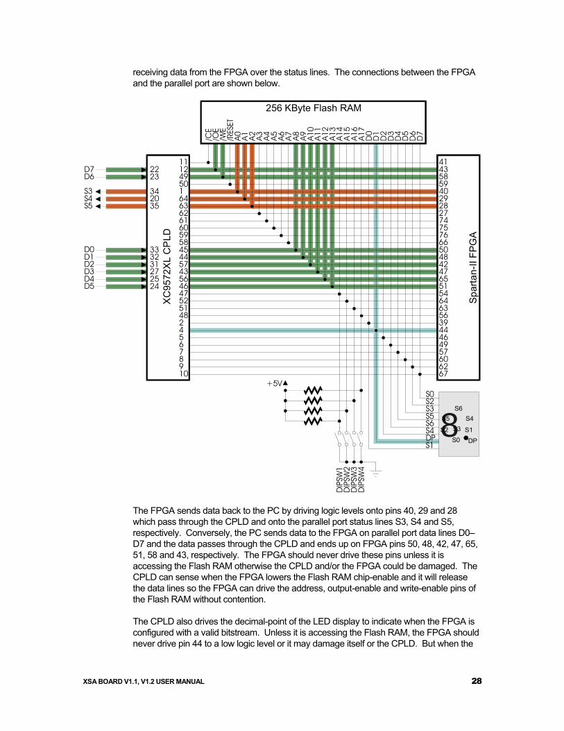
receiving data from the FPGA over the status lines. The connections between the FPGA and the parallel port are shown below.
256 KByte Flash RAM
XC
9572
XL
CP
LD
A0/CE
1122
33
23
3231
34
27
20
25
35
24
4
S2
9
DP
8
S4
7
S6
6
S5
5
S3
2
S0+5V
48515247465643
12
5744455859606162636415049
10
S1
D0
D0A2/WE
D2
D2A3/RESET
D3
D3
S3
A4 D4
D4
S4
A5 D5
D5
S5
A6 D6
D6
A7 D7
D7
A8 A9A1/OE
D1
D1
A10
A11
A12
A13
A14
A15
A16
A17
8S1
DP
S2 S3S4S5
S6
S0
DIPSW
4DIPSW
3DIPSW
2DIPSW
1
Spar
tan-
II FP
GA
41
44
6260574946
3956636454516547
43
42485066767574272829405958
67
The FPGA sends data back to the PC by driving logic levels onto pins 40, 29 and 28 which pass through the CPLD and onto the parallel port status lines S3, S4 and S5, respectively. Conversely, the PC sends data to the FPGA on parallel port data lines D0–D7 and the data passes through the CPLD and ends up on FPGA pins 50, 48, 42, 47, 65, 51, 58 and 43, respectively. The FPGA should never drive these pins unless it is accessing the Flash RAM otherwise the CPLD and/or the FPGA could be damaged. The CPLD can sense when the FPGA lowers the Flash RAM chip-enable and it will release the data lines so the FPGA can drive the address, output-enable and write-enable pins of the Flash RAM without contention.
The CPLD also drives the decimal-point of the LED display to indicate when the FPGA is configured with a valid bitstream. Unless it is accessing the Flash RAM, the FPGA should never drive pin 44 to a low logic level or it may damage itself or the CPLD. But when the
XSA BOARD V1.1, V1.2 USER MANUAL 28
FPGA lowers the Flash RAM chip-enable, the CPLD will stop driving the LED decimal-point to allow the FPGA access to data pin D1 of the Flash RAM.
For more details on how the CPLD manages the interface between the parallel port and the SpartanII FPGA both before and after device configuration, see the XSA Parallel Port Interface application note.
Prototyping Header
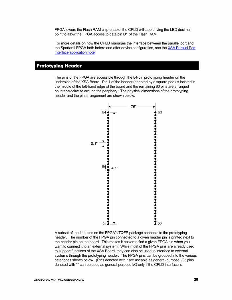
The pins of the FPGA are accessible through the 84-pin prototyping header on the underside of the XSA Board. Pin 1 of the header (denoted by a square pad) is located in the middle of the left-hand edge of the board and the remaining 83 pins are arranged counter-clockwise around the periphery. The physical dimensions of the prototyping header and the pin arrangement are shown below.
1
21 22
6364
84
1.75"
4.1"
0.1"
A subset of the 144 pins on the FPGA’s TQFP package connects to the prototyping header. The number of the FPGA pin connected to a given header pin is printed next to the header pin on the board. This makes it easier to find a given FPGA pin when you want to connect it to an external system. While most of the FPGA pins are already used to support functions of the XSA Board, they can also be used to interface to external systems through the prototyping header. The FPGA pins can be grouped into the various categories shown below. (Pins denoted with * are useable as general-purpose I/O; pins denoted with ** can be used as general-purpose I/O only if the CPLD interface is
XSA BOARD V1.1, V1.2 USER MANUAL 29
reprogrammed with the alternate parallel port interface stored in the dwnldpa2.svf file; pins with no marking cannot be used as general-purpose I/O at all.)
Configuration Pins (30*, 31*, 37, 38*, 39*, 44*, 46*, 49*, 57*, 60*, 62*, 67*, 68*, 69, 72, 106, 109, 111): These pins are used to load the SpartanII FPGA with a configuration bitstream. Some of these pins are dedicated to the configuration process and cannot be used as general-purpose I/O (37, 69, 72, 106, 109, 111). The rest can be used as general-purpose I/O after the FPGA is configured. If external logic is connected to these pins, you may have to disable it during the configuration process. The DONE pin (72) can be used for this purpose since it goes to a logic high only after the configuration process is completed.
Flash RAM Pins (27*, 28*, 29*, 39*, 40*, 41*, 42**, 43**, 44*, 46*, 47**, 48**, 49*, 50**, 51**, 54*, 56*, 57*, 58**, 59*, 60*, 62*, 63*, 64*, 65**, 66*, 67*, 74*, 75*, 76*): These pins are used by the FPGA to access the Flash RAM. They can be used for general-purpose I/O under the following conditions. When the FPGA is configured from the Flash, the CPLD drives all these pins so any external logic should be disabled using the DONE pin. Also, after the configuration, the Flash chip-enable (41) should be driven high to disable the Flash RAM so it doesn’t drive the data bus pins. In addition, the standard parallel port interface loaded into the CPLD (dwnldpar.svf) will drive eight of the Flash RAM pins (42, 43, 47, 48, 50, 51, 58, 65) with the logic values found on the eight data lines of the parallel port. If this is not desired, then use the alternate parallel port interface (dwnldpa2.svf) which does not drive these pins.
VGA Pins (12*, 13*, 19*, 20*, 21*, 22*, 23*, 26*): When not used to drive a VGA monitor, these pins can be used for general-purpose I/O through the prototyping header. When used as I/O, the RED0–RED1 (12–13), GREEN0–GREEN1 (19–20) and BLUE0–BLUE1 (21–22) pairs have an impedance of approximately 1 KΩ between them due to the presence of the resistor-ladder DAC circuitry.
PS/2 Pins (93*, 94*): When not used to access the PS/2 keyboard/mouse port, these pins can be used as general-purpose I/O through the prototyping header.
Global Clock Pins (15*, 18*): These pins can be used as global clock inputs or general-purpose inputs. They cannot be used as outputs.
Free Pins (77*, 78*, 79*, 80*, 83*, 84*, 85*, 86*, 87*): These pins are not connected to any other devices on the XSA Board so they can be used without restrictions as general-purpose I/O through the prototyping header.
JTAG Pins (2, 32, 34, 142): These pins are used to access the JTAG features of the FPGA. They cannot be used as general-purpose I/O pins.
XSA BOARD V1.1, V1.2 USER MANUAL 30
A XSA Pin Connections
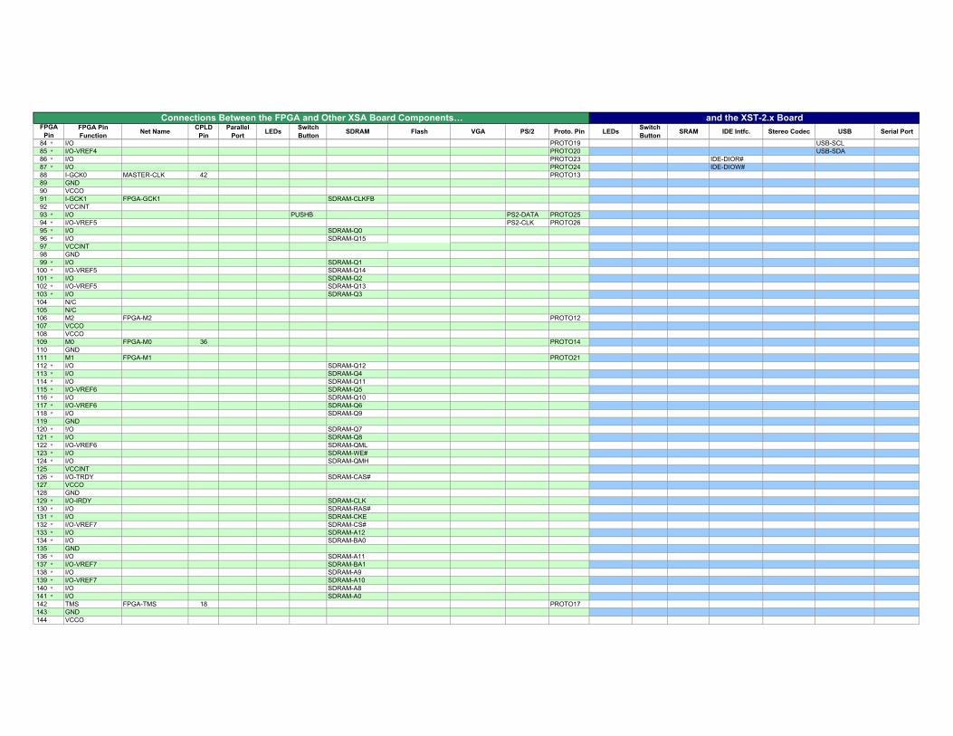
The following tables list the pin numbers of the FPGA and CPLD along with the pin names of the other chips that they connect to on the XSA Board and the XStend Board. The first two tables correspond to an XSA Board + XST-2.x combination, while the last two tables correspond to an XSA Board + XST-1.x combination. Pins marked with * are useable as general-purpose I/O; pins denoted with ** can be used as general-purpose I/O only if the CPLD interface is reprogrammed with the alternate parallel port interface stored in the dwnldpa2.svf file; pins with no marking cannot be used as general-purpose I/O at all.
XSA BOARD V1.1, V1.2 USER MANUAL 31
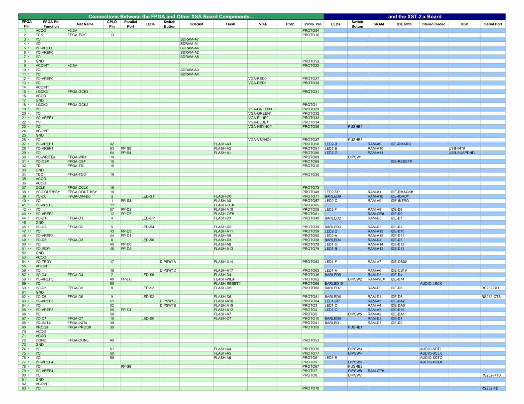
FPGA Pin Function Net Name CPLD
PinParallel
Port LEDs Switch Button SDRAM Flash VGA PS/2 Proto. Pin LEDs Switch
Button SRAM IDE Intfc. Stereo Codec USB Serial Port
1 VCCO +3.3V PROTO542 TCK FPGA-TCK 13 PROTO163 * I/O SDRAM-A74 * I/O SDRAM-A15 * I/O-VREF0 SDRAM-A66 * I/O-VREF0 SDRAM-A27 * I/O SDRAM-A58 GND PROTO529 VCCINT +2.5V PROTO2210 * I/O SDRAM-A311 * I/O SDRAM-A412 * I/O-VREF0 VGA-RED0 PROTO2713 * I/O VGA-RED1 PROTO2814 VCCINT15 * I-GCK3 FPGA-GCK3 PROTO3116 VCCO17 GND18 * I-GCK2 FPGA-GCK2 PROTO119 * I/O VGA-GREEN0 PROTO2920 * I/O VGA-GREEN1 PROTO3221 * I/O-VREF1 VGA-BLUE0 PROTO3322 * I/O VGA-BLUE1 PROTO3423 * I/O VGA-HSYNC# PROTO36 PUSHB424 VCCINT25 GND26 * I/O VGA-VSYNC# PROTO37 PUSHB327 * I/O-VREF1 62 FLASH-A3 PROTO50 LED2-B RAM-A0 IDE-DMARQ28 * I/O-VREF1 63 PP-S5 FLASH-A2 PROTO51 LED2-E RAM-A10 USB-INT#29 * I/O 64 PP-S4 FLASH-A1 PROTO56 LED2-G RAM-A11 USB-SUSPEND30 * I/O-WRITE# FPGA-WR# 19 PROTO69 DIPSW131 * I/O-CS# FPGA-CS# 15 PROTO68 IDE-RESET#32 TDI FPGA-TDI 15 PROTO1533 GND34 TDO FPGA-TDO 19 PROTO3035 VCCO36 VCCO37 CCLK FPGA-CCLK 16 PROTO7338 * I/O-DOUT/BSY FPGA-DOUT-BSY 18 PROTO45 LED2-DP RAM-A1 IDE-DMACK#39 * I/O-D0 FPGA-DIN-D0 2 LED-S1 FLASH-D0 PROTO71 BARLED9 RAM-A16 IDE-IORDY40 * I/O 1 PP-S3 FLASH-A0 PROTO57 LED2-C RAM-A9 IDE-INTRQ41 * I/O-VREF2 11 FLASH-CE# PROTO6542 ** I/O 57 PP-D2 FLASH-A10 PROTO58 LED2-F RAM-A8 IDE-D843 ** I/O-VREF2 12 PP-D7 FLASH-OE# PROTO61 RAM-OE# IDE-D944 * I/O-D1 FPGA-D1 4 LED-DP FLASH-D1 PROTO40 BARLED2 RAM-D6 IDE-D145 GND46 * I/O-D2 FPGA-D2 5 LED-S4 FLASH-D2 PROTO39 BARLED3 RAM-D5 IDE-D247 ** I/O 43 PP-D3 FLASH-A11 PROTO59 LED2-D RAM-A13 IDE-D1048 ** I/O-VREF2 44 PP-D1 FLASH-A9 PROTO60 LED2-A RAM-A15 IDE-D1149 * I/O-D3 FPGA-D3 6 LED-S6 FLASH-D3 PROTO38 BARLED4 RAM-D4 IDE-D350 ** I/O 45 PP-D0 FLASH-A8 PROTO78 LED1-G RAM-A14 IDE-D1251 ** I/O-IRDY 46 PP-D5 FLASH-A13 PROTO79 LED1-B RAM-A12 IDE-D1352 GND53 VCCO54 * I/O-TRDY 47 DIPSW1A FLASH-A14 PROTO82 LED1-F RAM-A7 IDE-CS0#55 VCCINT56 * I/O 48 DIPSW1D FLASH-A17 PROTO83 LED1-A RAM-A6 IDE-CS1#57 * I/O-D4 FPGA-D4 7 LED-S5 FLASH-D4 PROTO35 BARLED5 RAM-D3 IDE-D458 ** I/O-VREF3 49 PP-D6 FLASH-WE# PROTO62 DIPSW2 RAM-WE# IDE-D1459 * I/O 50 FLASH-RESET# PROTO66 BARLED10 AUDIO-LRCK60 * I/O-D5 FPGA-D5 8 LED-S3 FLASH-D5 PROTO80 BARLED7 RAM-D0 IDE-D6 RS232-RD61 GND62 * I/O-D6 FPGA-D6 9 LED-S2 FLASH-D6 PROTO81 BARLED6 RAM-D1 IDE-D5 RS232-CTS63 * I/O-VREF3 51 DIPSW1C FLASH-A16 PROTO84 LED1-DP RAM-A5 IDE-DA264 * I/O 52 DIPSW1B FLASH-A15 PROTO3 LED1-D RAM-A4 IDE-DA065 ** I/O-VREF3 56 PP-D4 FLASH-A12 PROTO4 LED1-C RAM-A3 IDE-D1566 * I/O 58 FLASH-A7 PROTO5 DIPSW5 RAM-A2 IDE-DA167 * I/O-D7 FPGA-D7 10 LED-S0 FLASH-D7 PROTO10 BARLED8 RAM-D2 IDE-D768 * I/O-INIT# FPGA-INIT# 38 PROTO41 BARLED1 RAM-D7 IDE-D069 PROG# FPGA-PROG# 39 PROTO55 PUSHB170 VCCO71 VCCO72 DONE FPGA-DONE 40 PROTO5373 GND74 * I/O 61 FLASH-A4 PROTO70 DIPSW3 AUDIO-SDTI75 * I/O 60 FLASH-A5 PROTO77 DIPSW4 AUDIO-SCLK76 * I/O 59 FLASH-A6 PROTO6 LED1-E AUDIO-SDTO77 * I/O-VREF4 PROTO9 DIPSW6 AUDIO-MCLK78 * I/O PP-S6 PROTO67 PUSHB279 * I/O-VREF4 PROTO7 DIPSW8 RAM-CE#80 * I/O PROTO8 DIPSW7 RS232-RTS81 GND82 VCCINT83 * I/O PROTO18 RS232-TD
Connections Between the FPGA and Other XSA Board Components… and the XST-2.x BoardFPGA
Pin
FPGA Pin Function Net Name CPLD
PinParallel
Port LEDs Switch Button SDRAM Flash VGA PS/2 Proto. Pin LEDs Switch
Button SRAM IDE Intfc. Stereo Codec USB Serial Port
Connections Between the FPGA and Other XSA Board Components… and the XST-2.x BoardFPGA
Pin84 * I/O PROTO19 USB-SCL85 * I/O-VREF4 PROTO20 USB-SDA86 * I/O PROTO23 IDE-DIOR#87 * I/O PROTO24 IDE-DIOW#88 I-GCK0 MASTER-CLK 42 PROTO1389 GND90 VCCO91 I-GCK1 FPGA-GCK1 SDRAM-CLKFB92 VCCINT93 * I/O PUSHB PS2-DATA PROTO2594 * I/O-VREF5 PS2-CLK PROTO2695 * I/O SDRAM-Q096 * I/O SDRAM-Q1597 VCCINT98 GND99 * I/O SDRAM-Q1100 * I/O-VREF5 SDRAM-Q14101 * I/O SDRAM-Q2102 * I/O-VREF5 SDRAM-Q13103 * I/O SDRAM-Q3104 N/C105 N/C106 M2 FPGA-M2 PROTO12107 VCCO108 VCCO109 M0 FPGA-M0 36 PROTO14110 GND111 M1 FPGA-M1 PROTO21112 * I/O SDRAM-Q12113 * I/O SDRAM-Q4114 * I/O SDRAM-Q11115 * I/O-VREF6 SDRAM-Q5116 * I/O SDRAM-Q10117 * I/O-VREF6 SDRAM-Q6118 * I/O SDRAM-Q9119 GND120 * !/O SDRAM-Q7121 * I/O SDRAM-Q8122 * I/O-VREF6 SDRAM-QML123 * I/O SDRAM-WE#124 * I/O SDRAM-QMH125 VCCINT126 * I/O-TRDY SDRAM-CAS#127 VCCO128 GND129 * I/O-IRDY SDRAM-CLK130 * I/O SDRAM-RAS#131 * I/O SDRAM-CKE132 * I/O-VREF7 SDRAM-CS#133 * I/O SDRAM-A12134 * I/O SDRAM-BA0135 GND136 * I/O SDRAM-A11137 * I/O-VREF7 SDRAM-BA1138 * I/O SDRAM-A9139 * I/O-VREF7 SDRAM-A10140 * I/O SDRAM-A8141 * I/O SDRAM-A0142 TMS FPGA-TMS 18 PROTO17143 GND144 VCCO
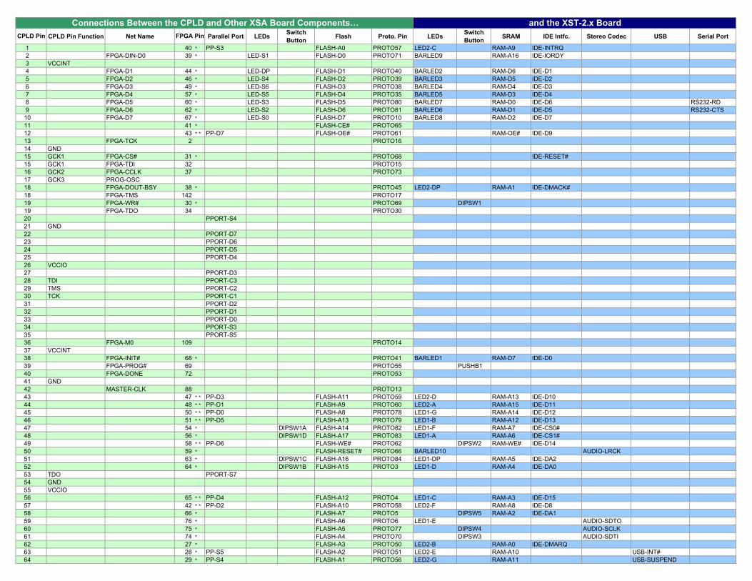
CPLD Pin Function Net Name Parallel Port LEDs Switch Button Flash Proto. Pin LEDs Switch
Button SRAM IDE Intfc. Stereo Codec USB Serial Port
1 40 * PP-S3 FLASH-A0 PROTO57 LED2-C RAM-A9 IDE-INTRQ2 FPGA-DIN-D0 39 * LED-S1 FLASH-D0 PROTO71 BARLED9 RAM-A16 IDE-IORDY3 VCCINT4 FPGA-D1 44 * LED-DP FLASH-D1 PROTO40 BARLED2 RAM-D6 IDE-D15 FPGA-D2 46 * LED-S4 FLASH-D2 PROTO39 BARLED3 RAM-D5 IDE-D26 FPGA-D3 49 * LED-S6 FLASH-D3 PROTO38 BARLED4 RAM-D4 IDE-D37 FPGA-D4 57 * LED-S5 FLASH-D4 PROTO35 BARLED5 RAM-D3 IDE-D48 FPGA-D5 60 * LED-S3 FLASH-D5 PROTO80 BARLED7 RAM-D0 IDE-D6 RS232-RD9 FPGA-D6 62 * LED-S2 FLASH-D6 PROTO81 BARLED6 RAM-D1 IDE-D5 RS232-CTS10 FPGA-D7 67 * LED-S0 FLASH-D7 PROTO10 BARLED8 RAM-D2 IDE-D711 41 * FLASH-CE# PROTO6512 43 ** PP-D7 FLASH-OE# PROTO61 RAM-OE# IDE-D913 FPGA-TCK 2 PROTO1614 GND15 GCK1 FPGA-CS# 31 * PROTO68 IDE-RESET#15 GCK1 FPGA-TDI 32 PROTO1516 GCK2 FPGA-CCLK 37 PROTO7317 GCK3 PROG-OSC18 FPGA-DOUT-BSY 38 * PROTO45 LED2-DP RAM-A1 IDE-DMACK#18 FPGA-TMS 142 PROTO1719 FPGA-WR# 30 * PROTO69 DIPSW119 FPGA-TDO 34 PROTO3020 PPORT-S421 GND22 PPORT-D723 PPORT-D624 PPORT-D525 PPORT-D426 VCCIO27 PPORT-D328 TDI PPORT-C329 TMS PPORT-C230 TCK PPORT-C131 PPORT-D232 PPORT-D133 PPORT-D034 PPORT-S335 PPORT-S536 FPGA-M0 109 PROTO1437 VCCINT38 FPGA-INIT# 68 * PROTO41 BARLED1 RAM-D7 IDE-D039 FPGA-PROG# 69 PROTO55 PUSHB140 FPGA-DONE 72 PROTO5341 GND42 MASTER-CLK 88 PROTO1343 47 ** PP-D3 FLASH-A11 PROTO59 LED2-D RAM-A13 IDE-D1044 48 ** PP-D1 FLASH-A9 PROTO60 LED2-A RAM-A15 IDE-D1145 50 ** PP-D0 FLASH-A8 PROTO78 LED1-G RAM-A14 IDE-D1246 51 ** PP-D5 FLASH-A13 PROTO79 LED1-B RAM-A12 IDE-D1347 54 * DIPSW1A FLASH-A14 PROTO82 LED1-F RAM-A7 IDE-CS0#48 56 * DIPSW1D FLASH-A17 PROTO83 LED1-A RAM-A6 IDE-CS1#49 58 ** PP-D6 FLASH-WE# PROTO62 DIPSW2 RAM-WE# IDE-D1450 59 * FLASH-RESET# PROTO66 BARLED10 AUDIO-LRCK51 63 * DIPSW1C FLASH-A16 PROTO84 LED1-DP RAM-A5 IDE-DA252 64 * DIPSW1B FLASH-A15 PROTO3 LED1-D RAM-A4 IDE-DA053 TDO PPORT-S754 GND55 VCCIO56 65 ** PP-D4 FLASH-A12 PROTO4 LED1-C RAM-A3 IDE-D1557 42 ** PP-D2 FLASH-A10 PROTO58 LED2-F RAM-A8 IDE-D858 66 * FLASH-A7 PROTO5 DIPSW5 RAM-A2 IDE-DA159 76 * FLASH-A6 PROTO6 LED1-E AUDIO-SDTO60 75 * FLASH-A5 PROTO77 DIPSW4 AUDIO-SCLK61 74 * FLASH-A4 PROTO70 DIPSW3 AUDIO-SDTI62 27 * FLASH-A3 PROTO50 LED2-B RAM-A0 IDE-DMARQ63 28 * PP-S5 FLASH-A2 PROTO51 LED2-E RAM-A10 USB-INT#64 29 * PP-S4 FLASH-A1 PROTO56 LED2-G RAM-A11 USB-SUSPEND
Connections Between the CPLD and Other XSA Board Components… and the XST-2.x BoardFPGA PinCPLD Pin
FPGA Pin Function Net Name CPLD
PinParallel
Port LEDs Switch Button SDRAM Flash VGA PS/2 Proto. Pin LEDs Switch Button SRAM VGA Stereo Codec PS/2 Xchecker
1 VCCO +3.3V PROTO542 TCK FPGA-TCK 13 PROTO16 XCHK-TCK3 * I/O SDRAM-A74 * I/O SDRAM-A15 * I/O-VREF0 SDRAM-A66 * I/O-VREF0 SDRAM-A27 * I/O SDRAM-A58 GND PROTO529 VCCINT +2.5V PROTO2210 * I/O SDRAM-A311 * I/O SDRAM-A412 * I/O-VREF0 VGA-RED0 PROTO2713 * I/O VGA-RED1 PROTO28 RLED-DP# RAM-A1514 VCCINT15 * I-GCK3 FPGA-GCK3 PROTO3116 VCCO17 GND18 * I-GCK2 FPGA-GCK2 PROTO119 * I/O VGA-GREEN0 PROTO2920 * I/O VGA-GREEN1 PROTO32 XCHK-RT21 * I/O-VREF1 VGA-BLUE0 PROTO3322 * I/O VGA-BLUE1 PROTO3423 * I/O VGA-HSYNC# PROTO3624 VCCINT25 GND26 * I/O VGA-VSYNC# PROTO37 PUSH-RESET#27 * I/O-VREF1 62 FLASH-A3 PROTO50 RLED-S4# RAM-A1228 * I/O-VREF1 63 PP-S5 FLASH-A2 PROTO51 RLED-S2# RAM-A1029 * I/O 64 PP-S4 FLASH-A1 PROTO56 RLED-S3# RAM-A1130 * I/O-WRITE# FPGA-WR# 19 PROTO69 DIPSW8 X-PS2-DATA31 * I/O-CS# FPGA-CS# 15 PROTO68 X-PS2-CLK32 TDI FPGA-TDI 15 PROTO15 XCHK-TDI33 GND34 TDO FPGA-TDO 19 PROTO30 XCHK-RD35 VCCO36 VCCO37 CCLK FPGA-CCLK 16 PROTO73 XCHK-CCLK38 * I/O-DOUT/BSY FPGA-DOUT-BSY 18 PROTO4539 * I/O-D0 FPGA-DIN-D0 2 LED-S1 FLASH-D0 PROTO71 XCHK-DIN40 * I/O 1 PP-S3 FLASH-A0 PROTO57 RLED-S1# RAM-A941 * I/O-VREF2 11 FLASH-CE# PROTO65 RAM-CE#42 ** I/O 57 PP-D2 FLASH-A10 PROTO58 RLED-S5# RAM-A1343 ** I/O-VREF2 12 PP-D7 FLASH-OE# PROTO61 RAM-OE#44 * I/O-D1 FPGA-D1 4 LED-DP FLASH-D1 PROTO40 BARLED2 RAM-D145 GND46 * I/O-D2 FPGA-D2 5 LED-S4 FLASH-D2 PROTO39 BARLED3 RAM-D247 ** I/O 43 PP-D3 FLASH-A11 PROTO59 RLED-S0# RAM-A848 ** I/O-VREF2 44 PP-D1 FLASH-A9 PROTO60 RLED-S6# RAM-A1449 * I/O-D3 FPGA-D3 6 LED-S6 FLASH-D3 PROTO38 BARLED4 RAM-D350 ** I/O 45 PP-D0 FLASH-A8 PROTO78 LLED-S3# RAM-A351 ** I/O-IRDY 46 PP-D5 FLASH-A13 PROTO79 LLED-S4# RAM-A452 GND53 VCCO54 * I/O-TRDY 47 DIPSW1A FLASH-A14 PROTO82 LLED-S5# RAM-A555 VCCINT56 * I/O 48 DIPSW1D FLASH-A17 PROTO83 LLED-S6# RAM-A657 * I/O-D4 FPGA-D4 7 LED-S5 FLASH-D4 PROTO35 BARLED5 RAM-D458 ** I/O-VREF3 49 PP-D6 FLASH-WE# PROTO62 RAM-WE#59 * I/O 50 FLASH-RESET# PROTO66 DIPSW7 CODEC-LRCK60 * I/O-D5 FPGA-D5 8 LED-S3 FLASH-D5 PROTO80 BARLED7 RAM-D661 GND62 * I/O-D6 FPGA-D6 9 LED-S2 FLASH-D6 PROTO81 BARLED6 RAM-D563 * I/O-VREF3 51 DIPSW1C FLASH-A16 PROTO84 LLED-DP# RAM-A764 * I/O 52 DIPSW1B FLASH-A15 PROTO3 LLED-S0# RAM-A065 ** I/O-VREF3 56 PP-D4 FLASH-A12 PROTO4 LLED-S1# RAM-A166 * I/O 58 FLASH-A7 PROTO5 LLED-S2# RAM-A267 * I/O-D7 FPGA-D7 10 LED-S0 FLASH-D7 PROTO10 BARLED8 RAM-D768 * I/O-INIT# FPGA-INIT# 38 PROTO41 BARLED1 RAM-D0 XCHK-INIT#69 PROG# FPGA-PROG# 39 PROTO55 PUSH-PROG# XCHK-PROG#70 VCCO71 VCCO72 DONE FPGA-DONE 40 PROTO53 XCHK-DONE73 GND74 * I/O 61 FLASH-A4 PROTO70 DIPSW6 CODEC-SDIN75 * I/O 60 FLASH-A5 PROTO77 DIPSW5 CODEC-SCLK76 * I/O 59 FLASH-A6 PROTO6 DIPSW4 CODEC-SDOUT77 * I/O-VREF4 PROTO9 DIPSW3 CODEC-MCLK XCHK-CLKO78 * I/O PP-S6 PROTO67 PUSH-SPARE# X-VGA-VSYNC#79 * I/O-VREF4 PROTO7 DIPSW1 RAM-LCE# XCHK-TRIG80 * I/O PROTO8 DIPSW2 RAM-RCE# XCHK-RST81 GND82 VCCINT83 * I/O PROTO18 X-VGA-RED184 * I/O PROTO19 X-VGA-HSYNC#85 * I/O-VREF4 PROTO20 X-VGA-GREEN1
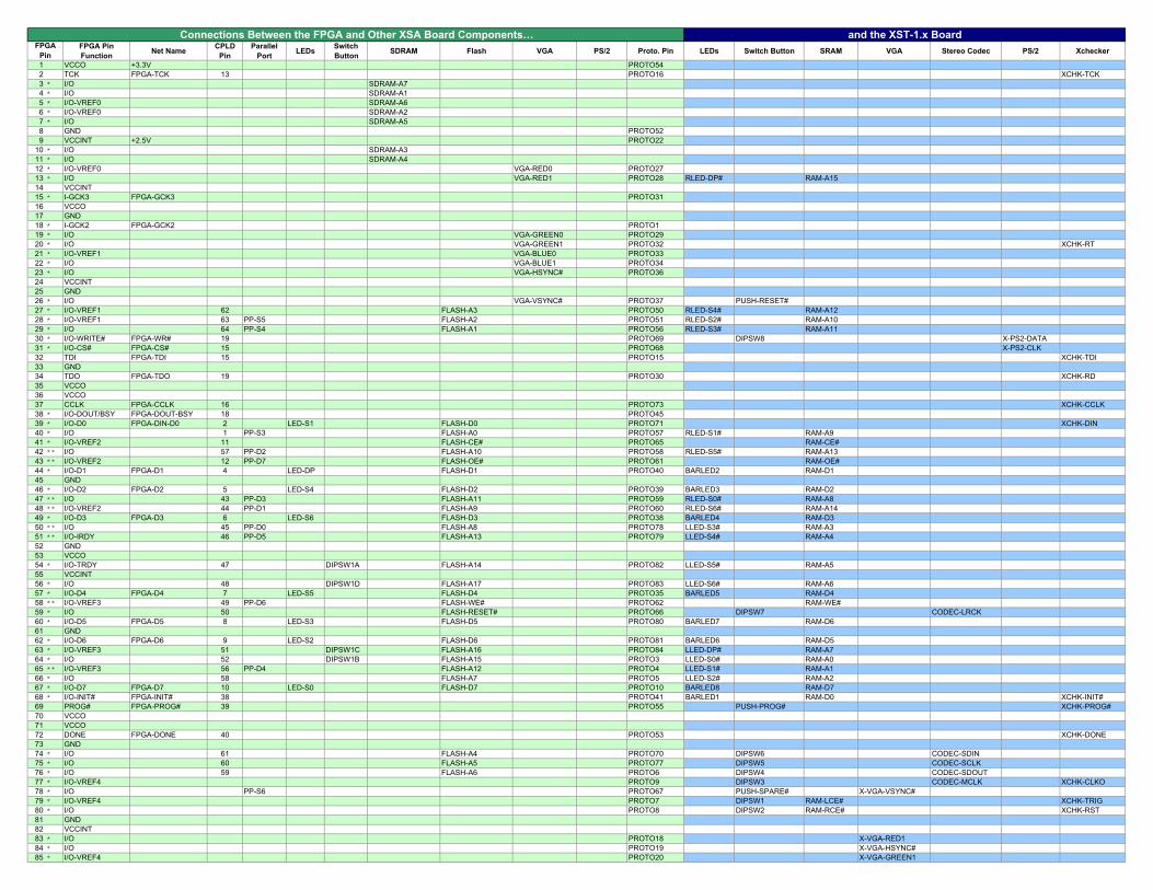
Connections Between the FPGA and Other XSA Board Components… and the XST-1.x BoardFPGA
Pin
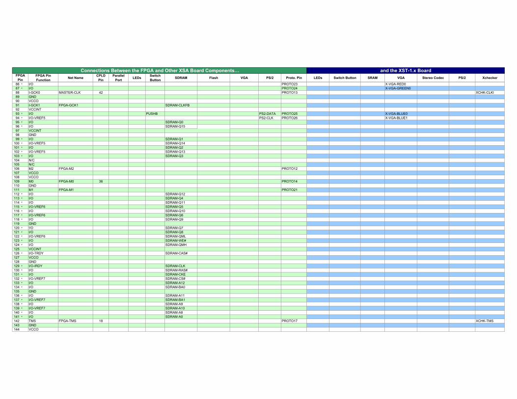
FPGA Pin Function Net Name CPLD
PinParallel
Port LEDs Switch Button SDRAM Flash VGA PS/2 Proto. Pin LEDs Switch Button SRAM VGA Stereo Codec PS/2 Xchecker
Connections Between the FPGA and Other XSA Board Components… and the XST-1.x BoardFPGA
Pin86 * I/O PROTO23 X-VGA-RED087 * I/O PROTO24 X-VGA-GREEN088 I-GCK0 MASTER-CLK 42 PROTO13 XCHK-CLKI89 GND90 VCCO91 I-GCK1 FPGA-GCK1 SDRAM-CLKFB92 VCCINT93 * I/O PUSHB PS2-DATA PROTO25 X-VGA-BLUE094 * I/O-VREF5 PS2-CLK PROTO26 X-VGA-BLUE195 * I/O SDRAM-Q096 * I/O SDRAM-Q1597 VCCINT98 GND99 * I/O SDRAM-Q1100 * I/O-VREF5 SDRAM-Q14101 * I/O SDRAM-Q2102 * I/O-VREF5 SDRAM-Q13103 * I/O SDRAM-Q3104 N/C105 N/C106 M2 FPGA-M2 PROTO12107 VCCO108 VCCO109 M0 FPGA-M0 36 PROTO14110 GND111 M1 FPGA-M1 PROTO21112 * I/O SDRAM-Q12113 * I/O SDRAM-Q4114 * I/O SDRAM-Q11115 * I/O-VREF6 SDRAM-Q5116 * I/O SDRAM-Q10117 * I/O-VREF6 SDRAM-Q6118 * I/O SDRAM-Q9119 GND120 * !/O SDRAM-Q7121 * I/O SDRAM-Q8122 * I/O-VREF6 SDRAM-QML123 * I/O SDRAM-WE#124 * I/O SDRAM-QMH125 VCCINT126 * I/O-TRDY SDRAM-CAS#127 VCCO128 GND129 * I/O-IRDY SDRAM-CLK130 * I/O SDRAM-RAS#131 * I/O SDRAM-CKE132 * I/O-VREF7 SDRAM-CS#133 * I/O SDRAM-A12134 * I/O SDRAM-BA0135 GND136 * I/O SDRAM-A11137 * I/O-VREF7 SDRAM-BA1138 * I/O SDRAM-A9139 * I/O-VREF7 SDRAM-A10140 * I/O SDRAM-A8141 * I/O SDRAM-A0142 TMS FPGA-TMS 18 PROTO17 XCHK-TMS143 GND144 VCCO
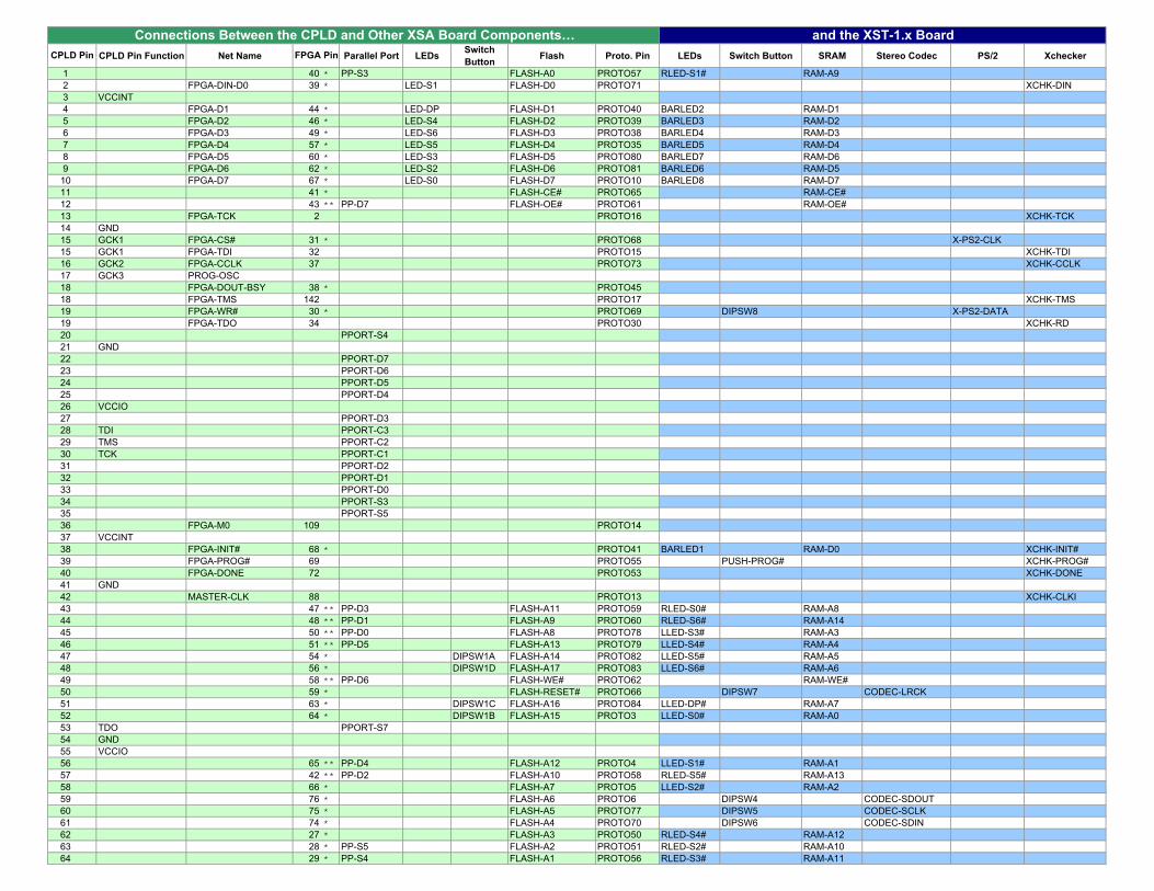
CPLD Pin Function Net Name Parallel Port LEDs Switch Button Flash Proto. Pin LEDs Switch Button SRAM Stereo Codec PS/2 Xchecker
1 40 * PP-S3 FLASH-A0 PROTO57 RLED-S1# RAM-A92 FPGA-DIN-D0 39 * LED-S1 FLASH-D0 PROTO71 XCHK-DIN3 VCCINT4 FPGA-D1 44 * LED-DP FLASH-D1 PROTO40 BARLED2 RAM-D15 FPGA-D2 46 * LED-S4 FLASH-D2 PROTO39 BARLED3 RAM-D26 FPGA-D3 49 * LED-S6 FLASH-D3 PROTO38 BARLED4 RAM-D37 FPGA-D4 57 * LED-S5 FLASH-D4 PROTO35 BARLED5 RAM-D48 FPGA-D5 60 * LED-S3 FLASH-D5 PROTO80 BARLED7 RAM-D69 FPGA-D6 62 * LED-S2 FLASH-D6 PROTO81 BARLED6 RAM-D510 FPGA-D7 67 * LED-S0 FLASH-D7 PROTO10 BARLED8 RAM-D711 41 * FLASH-CE# PROTO65 RAM-CE#12 43 ** PP-D7 FLASH-OE# PROTO61 RAM-OE#13 FPGA-TCK 2 PROTO16 XCHK-TCK14 GND15 GCK1 FPGA-CS# 31 * PROTO68 X-PS2-CLK15 GCK1 FPGA-TDI 32 PROTO15 XCHK-TDI16 GCK2 FPGA-CCLK 37 PROTO73 XCHK-CCLK17 GCK3 PROG-OSC18 FPGA-DOUT-BSY 38 * PROTO4518 FPGA-TMS 142 PROTO17 XCHK-TMS19 FPGA-WR# 30 * PROTO69 DIPSW8 X-PS2-DATA19 FPGA-TDO 34 PROTO30 XCHK-RD20 PPORT-S421 GND22 PPORT-D723 PPORT-D624 PPORT-D525 PPORT-D426 VCCIO27 PPORT-D328 TDI PPORT-C329 TMS PPORT-C230 TCK PPORT-C131 PPORT-D232 PPORT-D133 PPORT-D034 PPORT-S335 PPORT-S536 FPGA-M0 109 PROTO1437 VCCINT38 FPGA-INIT# 68 * PROTO41 BARLED1 RAM-D0 XCHK-INIT#39 FPGA-PROG# 69 PROTO55 PUSH-PROG# XCHK-PROG#40 FPGA-DONE 72 PROTO53 XCHK-DONE41 GND42 MASTER-CLK 88 PROTO13 XCHK-CLKI43 47 ** PP-D3 FLASH-A11 PROTO59 RLED-S0# RAM-A844 48 ** PP-D1 FLASH-A9 PROTO60 RLED-S6# RAM-A1445 50 ** PP-D0 FLASH-A8 PROTO78 LLED-S3# RAM-A346 51 ** PP-D5 FLASH-A13 PROTO79 LLED-S4# RAM-A447 54 * DIPSW1A FLASH-A14 PROTO82 LLED-S5# RAM-A548 56 * DIPSW1D FLASH-A17 PROTO83 LLED-S6# RAM-A649 58 ** PP-D6 FLASH-WE# PROTO62 RAM-WE#50 59 * FLASH-RESET# PROTO66 DIPSW7 CODEC-LRCK51 63 * DIPSW1C FLASH-A16 PROTO84 LLED-DP# RAM-A752 64 * DIPSW1B FLASH-A15 PROTO3 LLED-S0# RAM-A053 TDO PPORT-S754 GND55 VCCIO56 65 ** PP-D4 FLASH-A12 PROTO4 LLED-S1# RAM-A157 42 ** PP-D2 FLASH-A10 PROTO58 RLED-S5# RAM-A1358 66 * FLASH-A7 PROTO5 LLED-S2# RAM-A259 76 * FLASH-A6 PROTO6 DIPSW4 CODEC-SDOUT60 75 * FLASH-A5 PROTO77 DIPSW5 CODEC-SCLK61 74 * FLASH-A4 PROTO70 DIPSW6 CODEC-SDIN62 27 * FLASH-A3 PROTO50 RLED-S4# RAM-A1263 28 * PP-S5 FLASH-A2 PROTO51 RLED-S2# RAM-A1064 29 * PP-S4 FLASH-A1 PROTO56 RLED-S3# RAM-A11
Connections Between the CPLD and Other XSA Board Components… and the XST-1.x BoardFPGA PinCPLD Pin
B XSA Schematics
The following pages show the detailed schematics for the XSA Board.
XSA BOARD V1.1, V1.2 USER MANUAL 32
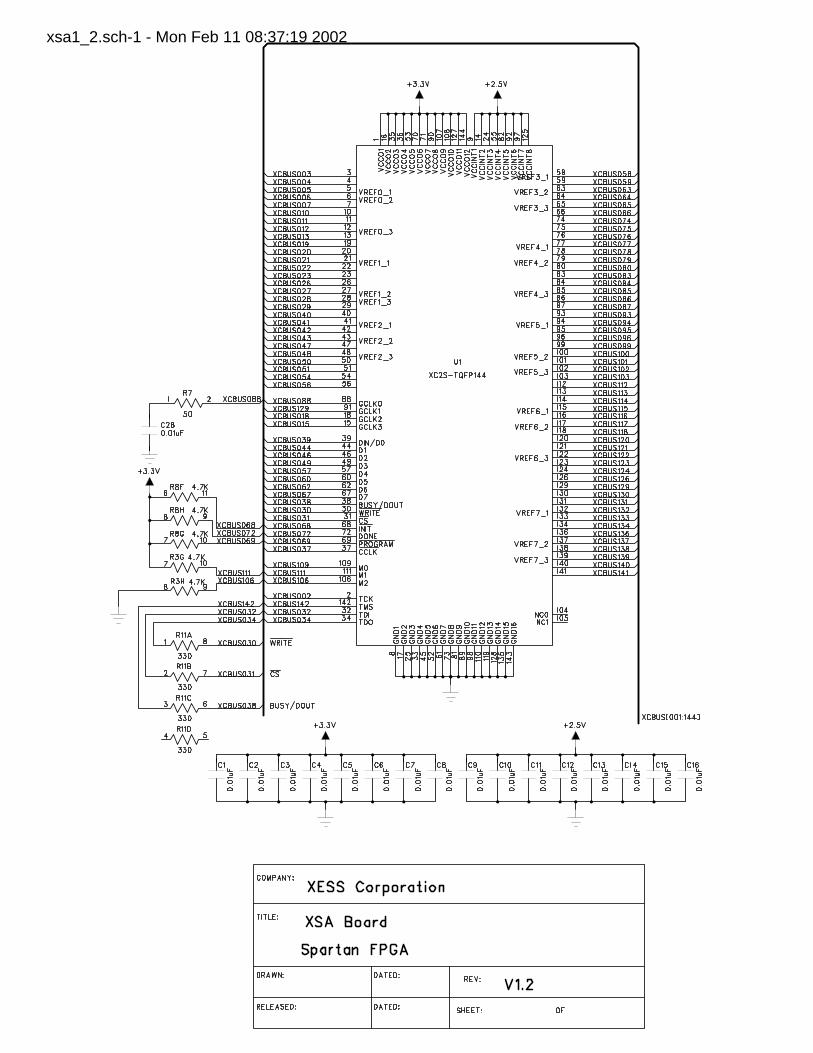
xsa1_2.sch-1 - Mon Feb 11 08:37:19 2002
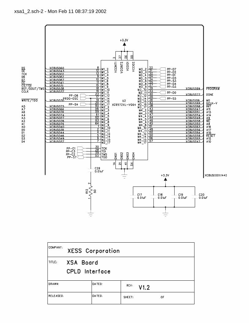
xsa1_2.sch-2 - Mon Feb 11 08:37:19 2002
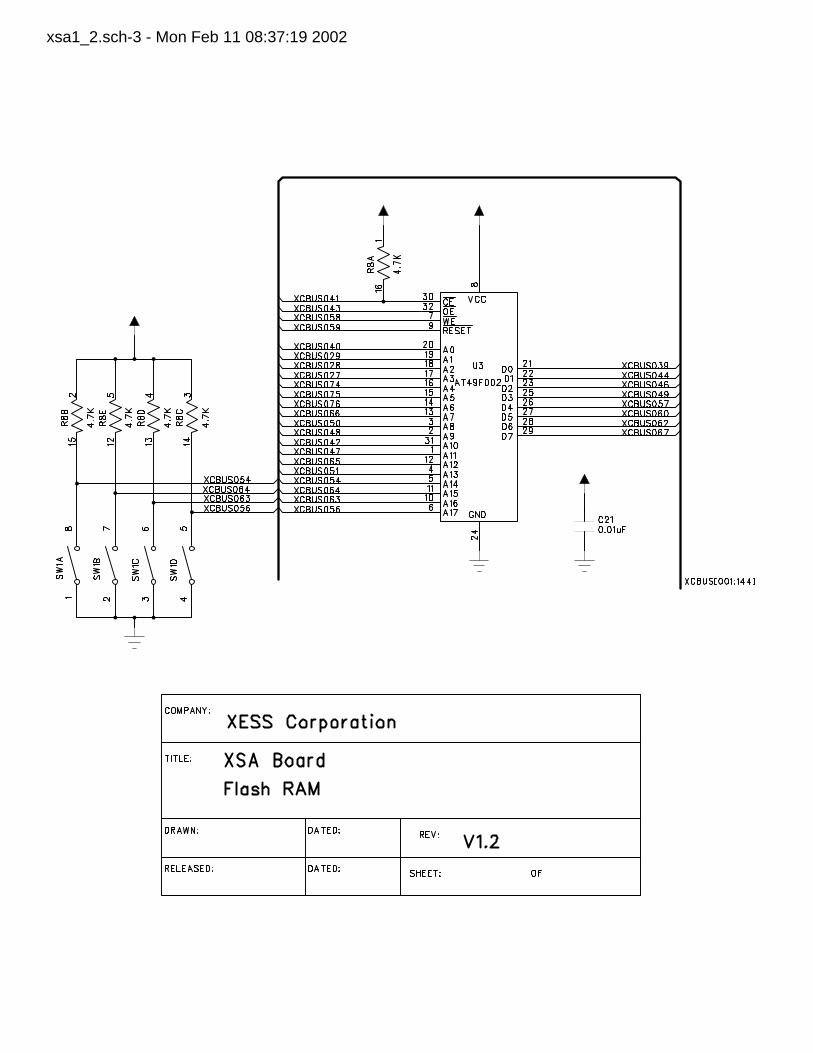
xsa1_2.sch-3 - Mon Feb 11 08:37:19 2002
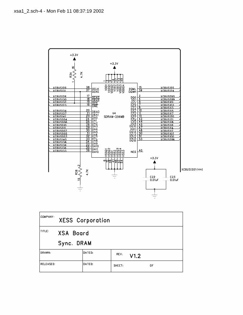
xsa1_2.sch-4 - Mon Feb 11 08:37:19 2002
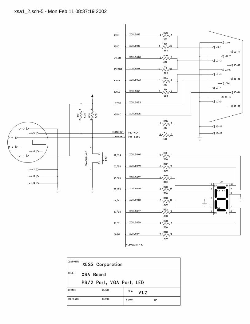
xsa1_2.sch-5 - Mon Feb 11 08:37:19 2002
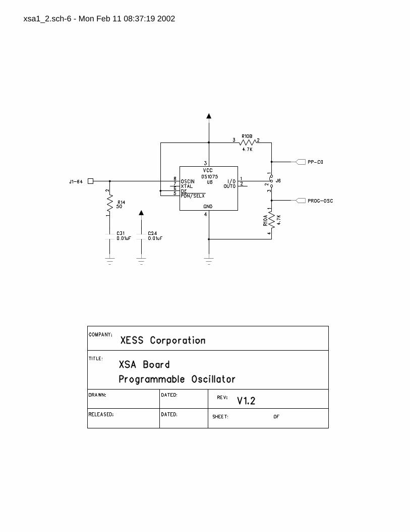
xsa1_2.sch-6 - Mon Feb 11 08:37:19 2002
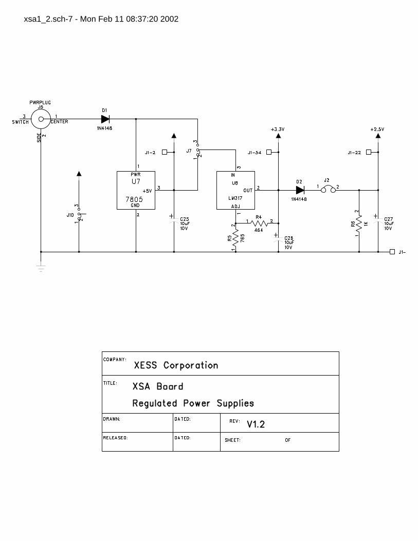
xsa1_2.sch-7 - Mon Feb 11 08:37:20 2002
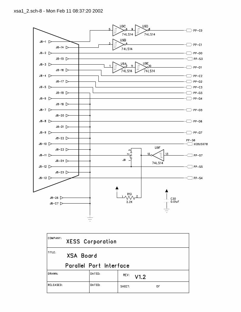
xsa1_2.sch-8 - Mon Feb 11 08:37:20 2002
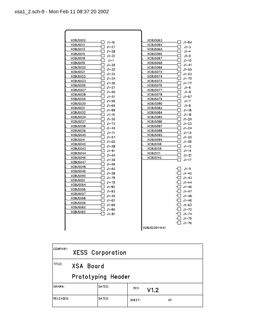
xsa1_2.sch-9 - Mon Feb 11 08:37:20 2002