z3$$11e0
TRANSCRIPT
ELECTRONICS
© COPYRIGHT BY ELETTRONICA VENETA SPA
32 BIT MICROPROCESSOR SYSTEM
module Z3/EV
Volume 1/4
THEORY AND EXERCISES
TEACHER/STUDENT manual

Z3$$11E0.DOC
INDEX
INDEX
Lesson F31: MICROCOMPUTER and MICROPROCESSORS Page. 1
Lesson F32: INTRODUCTION TO PROGRAMMING Page. 15
Lesson F33: PROGRAMMING in MACHINE CODE Page. 24
Lesson F34: PROGRAMMING in ASSEMBLER LANGUAGE Page. 33
Lesson F35: THE MICROPROCESSOR at 32 BIT 80386 Page. 42
Lesson F36: THE MICROPROCESSOR 80386EX Page. 56
Lesson F37: THE 32 BIT MICROPROCESSOR TRAINER Mod.Z3/EV Page. 68
Lesson F38: ADVANCED PROGRAMMING Page. 78
Lesson F39: INTERRUPTIONS MANAGEMENT Page. 88
Lesson F40: EPROM MEMORY and INTERFACING to the µP Page. 97
Lesson F41: RAM MEMORY and INTERFACING to the µP Page. 105
Lesson F42: PARALLEL INTERFACE Page. 115
INDEX
SAFETY RULES
Keep this handbook at hand for any further help.
After the packaging has been removed, set all accessories in order so thatthey are not lost and check the equipment integrity. In particular, checkthat it shows no visible damage.
Before connecting the equipment to the power supply, be sure that therating corresponds to the one of the power mains.
This equipment must be employed only for the use it has beenconceived, i.e. as educational equipment, and must be used under thedirect supervision of expert personnel.
Any other use is not proper and therefore dangerous. The manufacturercannot be held responsible for eventual damages due to inappropriate,wrong or unreasonable use.
Lesson F31: Microcomputer and Microprocessors
- 1 -
LESSON F31: MICROCOMPUTER and MICROPROCESSORS
OBJECTIVES• Type of computers: mainframe, minicomputer, personal computer,
microcomputer• Analysis of the microcomputer’s structure• Development and type of microprocessors• The Intel x86 family• Internal architecture of the microprocessor 8086
MATERIALS
• Base unit for the IPES system (power supply mod.PS1-PSU/EV,module holder mod.MU/EV, individual management unitmod.SIS1/SIS2/SIS3)
• Experimentation module mod. Z3/EV
F31.1 TYPES of COMPUTERS Computers are available today in a variety of dimensions andperformances. They can be classified in the following way: - Mainframes - Minicomputers - Personal Computers - Microcomputers
MainFrames These are the biggest and most powerful computers; they can fill up aroom. Usually they use more processors in parallel and have enormousmemory dimensions. They are used in military applications, in data management of largecompanies, etc. Examples of this type are IBM 4381, the Cray Y-MP/832.
Minicomputers These are less powerful computers and of smaller dimensions than themainframes. Usually they are contained in a single rack. They have data words of 64 bit and less memory than the mainframes. They are used for data management and as graphic stations. Examples of this type are VAX of Digital.
Personal Computer These computers are used the most. They use processors with 64 bitdata words (Pentium), central memory in the order of some tens MBand mass memory of some GB.

Lesson F31: Microcomputer and Microprocessors
- 2 -
Microcomputers These are the smallest computers, generally used in industrialapplications. Their structure handles a single card containing the microprocessor, theEPROM memory and RAM and the I/O devices. They use data words of 8, 16, 32 bytes and memories of some tens KB. The 32 Bit Microprocessor Trainer is an example of a microcomputer.
F31.2 THE STRUCTURE OF THE MICROCOMPUTER
The structure of a simple microcomputer is shown in figure F31.1:
fig. F31.1
In it, there’s to note:- The Central Processing Unit- The Memories (RAM and EPROM)- The Input/Output ports- The Connection Bus (Data, Addresses, Control)
THE CENTRAL PROCESSING UNIT (CPU) The CPU controls the operations of the microcomputer and is composedof a microprocessor. It takes the instructions in binary format from the memory andtransforms it in a series of actions that are followed sequentially.
Memory (RAM and EPROM) The memory consists generally of a mixture between RAM andEPROM (o ROM). The EPROM contains the binary code of the instructions sequencewhich the microprocessor has to follow (this memory needs to be onlyread). The RAM memory contains the data that is elaborated during theexecution of the program (this memory should be read and written).
Input/Output Ports The Input/Output ports allow the computer to take data from theexternal world and to send data to the external world. The devices used by the computer to connect themselves with externaldevices are called ports.

Lesson F31: Microcomputer and Microprocessors
- 3 -
An input port allows to read data from a keyboard or from an A/Dconverter. An output port allows to send data to a terminal, to a D/A converter, etc.
Connection Bus (Addresses, Data, Control) The connection bus is formed by signal lines in parallel (8, 16, 20, 32,etc.) that allow communication between the microprocessor and all theother elements present inside the microcomputer. Bus Addresses. It is used by the CPU to indicate the address of the memory location thatis to be read or written. The number of memory locations that the CPU is able to locate dependson the number of address lines. Some examples are shown next:0
Address lines Memory Locations 16 64 KB 20 1 MB 24 16 MB
The address bus is unidirectional: comes out from the microprocessorand goes towards the memory devices and I/O. Data Bus. It is used by the CPU to read and write data from the memory and fromthe I/O ports. Consists of 8, 16, 32 lines in parallel. All the memory devices and of I/O have their outputs connected to thedata bus, but only one of them has its output enabled at a certain instant. The devices that have their outputs enabled have to be in the conditioncalled three-state. Control Bus. Consists in a number of lines between 4 and 12 that allow themicroprocessor to indicate to the memory and the peripherals, thecurrent operations. Typical control signals are: Memory Read, Memory Write, I/O Read,I/O Write.
F31.3 EVOLUTION AND MICROPROCESSORS TYPES
It’s been seen how the microprocessor composes the CPU of amicrocomputer. There are many microprocessors available today, with differentcharacteristics. These have evolved in time with a progressive increasein their performance. The following table shows some of these microprocessors with its maincharacteristics:

Lesson F31: Microcomputer and Microprocessors
- 4 -
Micro processor
Characteristics
4004 It was the first microprocessor commercially available (in1971). It was a 4-bit microprocessor (Intel).
8008 Evolution to 8 bit from the preceding one (1972). 8080 Microprocessor Intel including 8 bit (1974). It was the
beginning of the microprocessors of the second generation. 6800 Microprocessor Motorola of 8 bit. 6502 Microprocessor of 8 bit used in the first Apple PC. Z80 Microprocessor Zilog of 8 bit. 6809 Microprocessor Motorola of 8 bit with instructions of 16
bit. 8088 Microprocessor Intel of 16 bit internal and 8 bit external
(used in the first IBM PC) 8086 Microprocessor Intel of 16 bit. 80286 Microprocessor Intel of 16 bit with advanced addressing
capacity and memory management 80386 Microprocessor Intel of 32 bit 68020 Microprocessor Motorola of 32 bit 32032 Microprocessor National of 32 bit 80486 Microprocessor Intel of 32 bit with added performance
(mathematical coprocessor) Pentium Microprocessor Intel of 64 bit
F31.4 The Intel x86 Family
In the preceding table some of the Intel microprocessors have beenshown, whose code name end with number 86. These are part of asingle microprocessors family called x86. Next, we will describe in detail the family components with their maincharacteristics. 8086 It’s a microprocessor of 16 bit. The Arithmetic Logic Unit, the Registersand the Instructions are made for operating with 16 bit words. It has an external data bus of 16 bit. It has an addresses bus of 20 bit, capable of addressing 1.048.576memory locations (1 MB). 8088 It’s the same as the preceding one, with the only difference that theexternal data bus is of 8 bit. 80186 It’s a more powerful version of microprocessor 8086. It contains internally some peripherals that are normally external. Its setof instructions is a superset from that of the ‘8086. That is, it maintainsthe software compatibility with the 8086.
Lesson F31: Microcomputer and Microprocessors
- 5 -
80286 It’s a 16-bit microprocessor projected to be used in multi-user andmultitasking applications. When it operates in real address mode behaves like a 8086, but faster. When it operates in its virtual address mode allows to keep moreprograms in memory, separating and protecting one from the other. 80386 It’s a 32-bit microprocessor that can address directly up to 32 GBmemory. It’s composed of 32 data lines and of 32 address lines. Allows to operate in real address mode behaving like a 8086, but morepowerful. 80486 It’s a step up version of the 486 that keeps all the characteristics of the386 with the addition of a mathematical coprocessor and a memorycache integrated manager. 80386EX It’s a particular version of the 386 that utilizes the same internal nuclei,with the addition of some integrated peripherals that simplify the insystems a microprocessor. This version is called Embedded and is particularly related to theindustrial world. The microprocessors 8086, 80286, 80386, 80486 aren’t used anymore inthe world of the Personal Computer (they were replaced by thePentium) and thus aren’t available in the market anymore. They continue to be available in their industrial versions like the386EX.
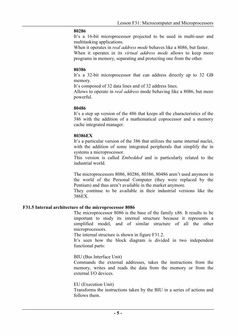
F31.5 Internal architecture of the microprocessor 8086 The microprocessor 8086 is the base of the family x86. It results to beimportant to study its internal structure because it represents asimplified model, and of similar structure of all the othermicroprocessors. The internal structure is shown in figure F31.2. It’s seen how the block diagram is divided in two independentfunctional parts: BIU (Bus Interface Unit) Commands the external addresses, takes the instructions from thememory, writes and reads the data from the memory or from theexternal I/O devices. EU (Execution Unit) Transforms the instructions taken by the BIU in a series of actions andfollows them.

Lesson F31: Microcomputer and Microprocessors
- 6 -
fig. F31.2
EU : (Execution Unit) Contains the following devices. Control System Guides and controls all the internal operations. Arithmetic/Logic Unit. Follows all the operations for sum, subtraction, AND, OR, XOR,increment, decrement, etc. Register of Flags. Contains the indications of the conditions produced by the execution ofthe instructions and the control of some operations of the EU. It is aregister of 16 bit with 9 active flags (see Fig. F31.3) . 6 flags (CF, PF, AF, ZF, SF, OF) are used to indicate the results of theinstruction operations. 3 flags (TF, IF, DF) are used to control determinate operations of theprocessor.

Lesson F31: Microcomputer and Microprocessors
- 7 -
fig. F31.3 Registers of general use. The EU contains 8 registers of general use, which can be divided as infigure F31.4:
fig. F31.4 I 4 registers of 16 bit of general use are called: AX = Primary accumulator BX = Accumulator and base register CX = Accumulator and counter DX = Accumulator and I/O addresser It can refer in an alternative way to each one of these registers as acouple of registers of 8 bit each (1 byte). The byte most to the left (themost significant) of the couple is defined as MSB, The byte most to theright, as LSB. Then the register AX can be separated in registers MSB: AH and LSB:AL.
Lesson F31: Microcomputer and Microprocessors
- 8 -
The register BX in BH and BL, etc. . There are two registers index of string, each one of them havingdimension of 16 bit. These are called SI (source index) and DI(destination index) and are frequently used to target the data strings inthe memory. These can be used as registers of general use of 16 bit. The register SP (stack pointer) is used for the implementation of a stackhardware in the memory (the description of the stack will be analyzedlater). It can be integrated by the register BP (base pointer) that can also beused as a register of 16 bit of general use.
BIU : Bus Interface Unit Contains the following devices. Queue While the EU is following an instruction that doesn’t need the use of thebus, the BIU takes from the memory up to a maximum of 6 bytesinstruction, for the following instructions. The BIU memorizes these bytes in a register FIFO called queue. Whenthe EU is ready for the next instruction, it simply reads the byte of theinstruction from the queue. This process, called pipelining, allows to follow the instructions in afaster way. Segment Registers The four segment registers (CS, DS, SS, ES) are special registersconnected to the data addressing of the external memory. Traditionally, the microprocessors always carry out the data acquisitionfrom the memory, using an address word of 16 bit. since the address is16 bit long, the maximum number of univoice addresses is 65536, or64K. The 8086 allows to address 1024KB (1 MB) of memory. It uses againan address word of 16 bit, but manages to address 1MB by means of amethod called memory address segmentation.
Lesson F31: Microcomputer and Microprocessors
- 9 -
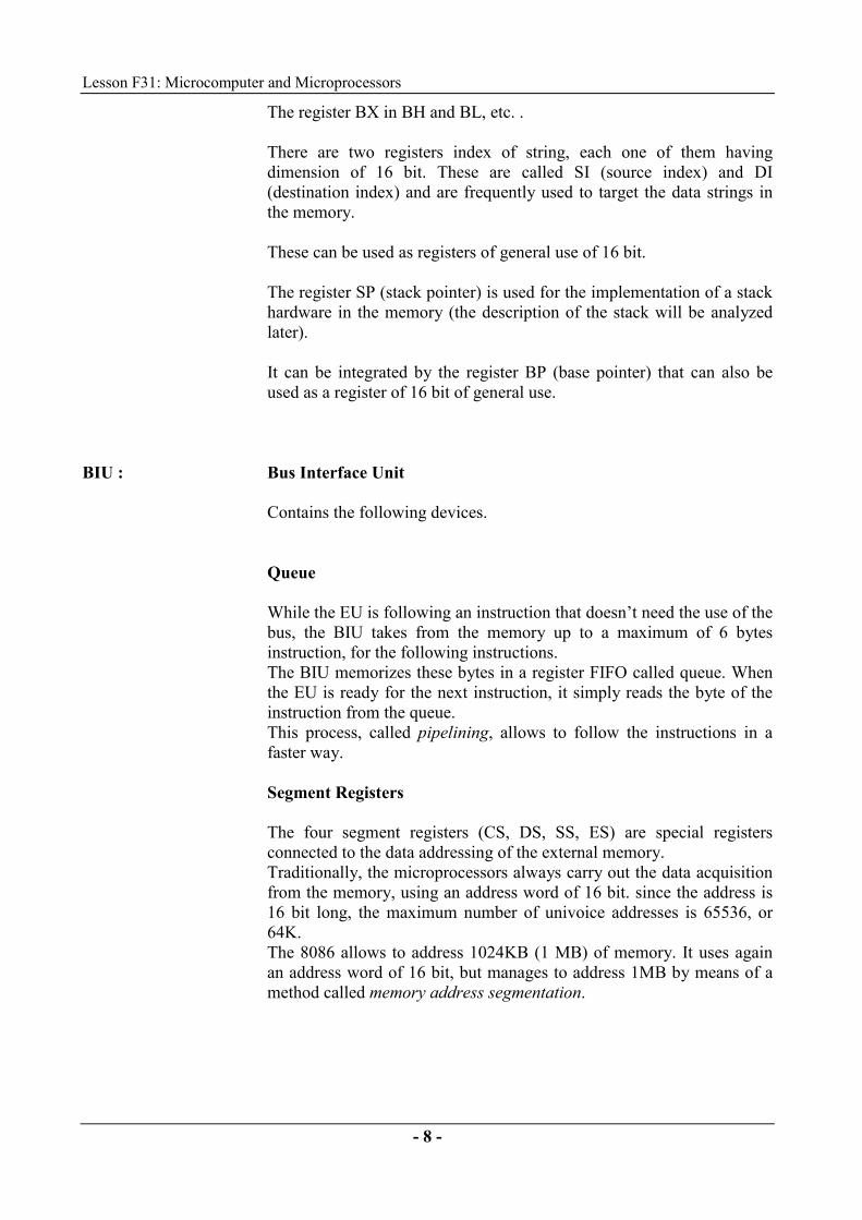
To address 1MB it’s necessaryto be able to represent thenumbers included between: 0 00000H 1048576 FFFFFH such operation requires 20 bit.The complete set of 1048576different addresses is a givenaddress apace of 1 megabyte.From the user’s point of view,the memory is addressed inblocks called SEGMENTS.
Fig.31.5
Each segment can contain up to 64KB data; this allows using thestandard 16 bit addressing within a segment.
Fig.31.6
A segment can contain only one, a hundred, or a thousand byte.
Additionally, the segments can be overlapped, that is, a data byte of datacan be accessible from more than one address of the segment beginning.
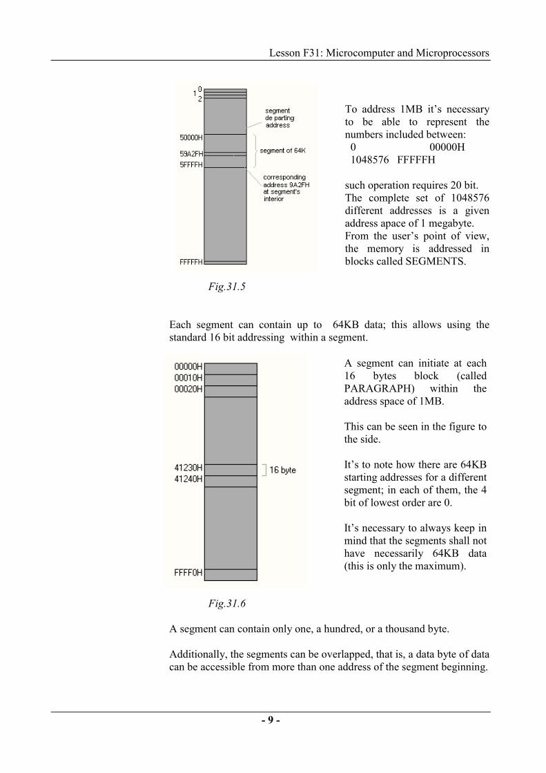
A segment can initiate at each16 bytes block (calledPARAGRAPH) within theaddress space of 1MB.
This can be seen in the figure tothe side.
It’s to note how there are 64KBstarting addresses for a differentsegment; in each of them, the 4bit of lowest order are 0.
It’s necessary to always keep inmind that the segments shall nothave necessarily 64KB data(this is only the maximum).
Lesson F31: Microcomputer and Microprocessors
- 10 -
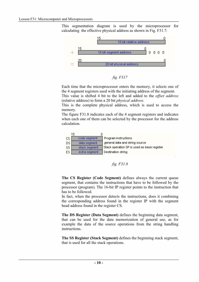
This segmentation diagram is used by the microprocessor forcalculating the effective physical address as shown in Fig. F31.7:
fig. F317 Each time that the microprocessor enters the memory, it selects one ofthe 4 segment registers used with the initiating address of the segment.This value is shifted 4 bit to the left and added to the offset address(relative address) to form a 20 bit physical address.This is the complete physical address, which is used to access thememory.The figure F31.8 indicates each of the 4 segment registers and indicateswhen each one of them can be selected by the processor for the addresscalculation.
fig. F31.8 The CS Register (Code Segment) defines always the current queuesegment, that contains the instructions that have to be followed by theprocessor (program). The 16-bit IP register points to the instruction thathas to be followed.In fact, when the processor detects the instructions, does it combiningthe corresponding address found in the register IP with the segmenthead address found in the register CS.
The DS Register (Data Segment) defines the beginning data segment,that can be used for the data memorization of general use, as forexample the data of the source operations from the string handlinginstructions.
The SS Register (Stack Segment) defines the beginning stack segment,that is used for all the stack operations.
Lesson F31: Microcomputer and Microprocessors
- 11 -
The register ES (Extra Segment) defines the extra segment, which canbe used as secondary area for general use data. The extra segment isalso used for the destination operations from the string handlinginstructions.
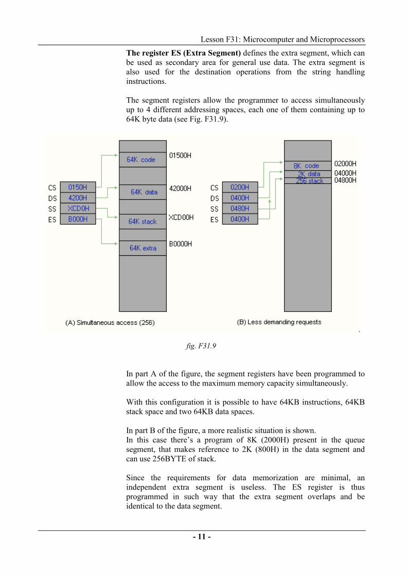
The segment registers allow the programmer to access simultaneouslyup to 4 different addressing spaces, each one of them containing up to64K byte data (see Fig. F31.9).
fig. F31.9 In part A of the figure, the segment registers have been programmed toallow the access to the maximum memory capacity simultaneously.
With this configuration it is possible to have 64KB instructions, 64KBstack space and two 64KB data spaces.
In part B of the figure, a more realistic situation is shown.In this case there’s a program of 8K (2000H) present in the queuesegment, that makes reference to 2K (800H) in the data segment andcan use 256BYTE of stack.
Since the requirements for data memorization are minimal, anindependent extra segment is useless. The ES register is thusprogrammed in such way that the extra segment overlaps and beidentical to the data segment.

Lesson F31: Microcomputer and Microprocessors
- 12 -
IP (Instruction Pointer)
As already seen, the instruction pointer IP contains the address at 16 bit,or offset, of the next code byte internal to the current segment.The effective address at 20 bit is obtained as seen beforehand.A usual way for representing a physical address at 20 bit is the form:
Segment: OffsetExamples:
CS:IP348A:4367
Lesson F31: Microcomputer and Microprocessors
- 13 -
F31.6 SUMMARY QUESTIONNAIRE
���� Z3
���� SIS1
���� SIS2 Insert Lesson Code: F31
Q1 How are called the microprocessor systems normally used in industrialapplications? SETA B 1 4 Mainframes 2 1 Minicomputers 3 3 Personal Computers 4 2 Microcomputers
Q2 Where is the data stored, which the microprocessor elaborates duringits functioning? SETA B 1 2 Memory EPROM 2 1 Memory RAM 3 4 Input/Output ports 4 3 Connection Bus
Q3 What is the fundamental difference between microprocessor 8088 andmicroprocessor 8086 ? SETA B1 2 The registers of the 8088 are of 8 bit and those of the 8086 of
16 bit2 4 The 8086 addresses a quantity of memory superior to the 8088’s 3 1 The 8088 has a data external Bus of 8 bit, the 8086 of 16 bit 4 3 The 8086 has a greater number of registers than the 8088’s
Lesson F31: Microcomputer and Microprocessors
- 14 -
Q4 Which of these registers isn’t part of the registers used by the EU
(Execution Unit) of the microprocessor 8086 ?SETA B1 3 Register IP2 1 Register SP3 4 Register AX4 5 Register SI5 2 Register BP
Q5 How many physical-addressing bits use the microprocessor 8086 for theaccess to the memory?SETA B1 2 8 bit2 1 16 bit3 5 20 bit4 3 24 bit5 4 32 bit
Q6 In a memory address specified as: 4AC2:6768, the value 4AC2represents ?SETA B1 5 The offset2 4 The register AX3 2 The segment register4 3 The accumulator5 1 The physical address
Q7 The name AL represents?SETA B1 3 the accumulator register2 4 The 8 bit most significant of the accumulator register3 1 The 8 bit least significant of the accumulator register4 2 The segment register associated to the accumulator
Q8 Which of the following physical memory addresses cannot be thestarting address of a segment ?SETA B1 2 0000H2 5 0001H3 1 0010H4 3 0100H5 4 1000H

Lesson F32: Introduction to Programing
- 15 -
LESSON F32: INTRODUCTION to PROGRAMMING
OBJECTIVES• Programming languages• Addressing modes• Immediate addressing mode• Register addressing mode• Direct in memory addressing mode• The microprocessor instructions
MATERIALS• base unit for system IPES (power supply mod.PS1-PSU/EV, module
holder mod.MU/EV, Individual Management Unitmod.SIS1/SIS2/SIS3)
• experimentation module mod.Z3/EV
F32.1 PROGRAMMING LANGUAGES After having analyzed the CPU 8086, we start analyzing itsprogramming in this lesson.there are 3 programming levels, which can be used:
• Machine Language• Assembler Language• High Level Languages
Machine Language Programs can be written simply by writing the binary codes of theinstructions that the microprocessor has to follow. An example is the following (operations done by the microprocessor areindicated among parenthesis, the numbers are in hexadecimal format): B0 24 (charges into register AL the number 24) E6 2F (output of register AL to the address port 2F)
This mode of operating is little efficient because the programmer has toknow the thousands of binary codes of the instructions ofmicroprocessor 8086.
Assembler Language In order to make programming easier, the programmers write theprograms in assembler language and then transform them in machinelanguage for its charging into the memory and execution. The assembler language uses two, three or four mnemonic letters for

Lesson F32: Introduction to Programing
- 16 -
representing each type of instruction. Each single instruction is written in a standard form that conceives 4fields as in figure:
Title Field
OperativeCod. Field
OperationsField
Comments Field
PRG: MOV AL,2FH ;charges AL con 2FH The two preceding instructions can be written as: PRG: MOV AL,24H ;charges the number 24H in AL OUT 2FH,AL ;sends AL to the port of num. 2FH
High Level Languages
Another way of writing the programs for the microprocessor is that ofusing high level languages as Pascal, COBOL or C. This type of programming is normally used by the Personal Computer. C language, very much close to the Assembler Language, is often usedalso with microcomputers. An appropriate compiler program transforms the instructions oflanguage C to machine code, for it to be followed by themicroprocessor.
F32.2 ADDRESSING MODES Before proceeding with the learning of the programming of themicroprocessor, it is necessary to analyze how the microprocessor canaccess to the data that has to elaborate.The different modes used to access data are called AddressingModes.If we consider, for example, the instruction MOV, it has the followingformat:
MOV destination, source
When it is followed, it copies a word (16 bit) or a byte (8 bit) from thespecified site as source, to the one specified as destination.The source can be a number, a register or a memory site specified bymeans of 24 different modes.The destination can be a register or a memory site specified by means of24 different modes.

Lesson F32: Introduction to Programing
- 17 -
F32.3 IMMEDIATE ADDRESSING MODE An immediate addressing mode takes place when the data that is wishedto be handled, is a number n specified directly in the instruction.Example:
MOV AX,043FH ;charges in AX the number 043F
The number 043F to be charged in the register is stored in the twomemory locations immediately following the code of the instructionMOV.
F32.4 REGISTER ADDRESSING MODE A register-addressing mode is when a register of the microprocessor isthe source of the operation of the instruction.Example:
MOV AX, BX; copies the register BX into register AX
This instruction copies the contents of register BX into register AX. Theregister BX remains unchanged.The instruction contains the codes for identifying the source register BXand the destination register AX.
F32.5 DIRECT ADDRESSING MODE into MEMORY
There are different modes to address data present in the memory. Nextwe will present the simplest mode. The other addressing modes will beanalyzed in upcoming lessons.
The direct addressing mode into memory consists of indicating theeffective address as a number of 16 bit directly into the instruction.Example:
MOV AX,[0421H] ;charges in AX the data to the site 0421
The square parentheses indicate: ‘the contents of the memory locationshas a shift respect the base segment of 0421H bytes’.
When this instruction is followed, the microprocessor executes thefollowing operations:
- takes the present value of the register DS (Data Segment), ex: 1234- shifts it 4 bit to the left: 12340- adds the value of the effective address: 0421- result of the sum: 12761
Lesson F32: Introduction to Programing
- 18 -
- this is the physical memory address of 20 bit.- takes the data to address 12761 and saves it in AL- takes the data to address 12762 and saves it in AH
In the preceding instruction the direct addressing specified the sourcedata of the instruction.Similarly, the destination can be specified:
MOV [0421H],AX ;charges to the site 0421 the register AX
F32.6 THE INSTRUCTIONS of the MICROPROCESSOR After having introduced the modes with which the microprocessoridentifies the data that has to elaborate, let’s see now which are theoperations that the microprocessor is capable of doing.We can say that:
The operations of a microprocessor correspond to its instructions.
Next we will show a table with the instructions of the microprocessor8086.Many of them will be used and analyzed in the following lessons.It is important here to give an overview of them to understand thepotentiality of this microprocessor.
INSTRUCTIONS of DATA TRANSFER
MOV Copies a byte or a word from a source to a destinationPUSH Copies a word specified on the stackPOP Copies a word from the stack to the specified sitePUSHA Copies all the registers on the stack (80186,..)POPA Copies from the stack to all the registers (80186, ..)XCHG Exchanges bytes or wordsXLAT Transforms a byte in AL using a table in the memoryIN Copies a byte or a word from the specified I/O port to the
accumulatorOUT Copies a byte or a word from the accumulator to the
specified I/O portLEA Charges the effective address of an operation in the
specified registerLDS Charges the register DS and other specified registers from
the memoryLES Charges the register ES and other specified registers from
the memoryLAHF Charges AH with the least significant byte of the flags
register

Lesson F32: Introduction to Programing
- 19 -
SAHF Memorizes AH in the least significant byte of the flagsregister
PUSHF Copies the flags register on the stackPOPF Copies a word from the stack to the flags register
ARITHMETIC INSTRUCTIONS
ADD Sums the specified byte/word to a byte/wordADC Sums considering also the value of the carry flagINC Increments the byte or the specified word in 1AAA Adjusting ASCII after an additionDAA Adjusting decimal after an additionSUB Subtracts the specified byte/ word to a byte/wordSBB Subtracts considering also the value of the carry flagDEC Decrements the byte or the specified word in 1NEG Calculates the complement to 2 of the specified byte/wordCMP Compares two byte or two wordsAAS Adjusting ASCII after a subtractionDAS Adjusting decimal after a subtractionMUL Multiplies bytes or words without signIMUL Multiplies bytes or words with signAAM Adjusting ASCII after the multiplicationDIV Divides a word without sign by a byte, or a double word
without sign by a wordIDIV Divides a word with sign by a byte, or a double word with
sign by a wordAAD Adjusting ASCII before the divisionCBW Fills the superior byte of a word with copies of the bit of
sign of the inferior byteCWD fills the superior word of a double word with the bit of
sign of the inferior word
BIT HANDLING INSTRUCTIONS
NOT Inverts each bit of a byte or of a wordAND Follows an AND of each bit of a byte or of a word with
the corresponding bit of a byte or of a wordOR Follows an OR of each bit of a byte or of a word with the
corresponding bit of a byte or of a wordXOR Follows an XOR of each bit of a byte or of a word with
the corresponding bit of a byte or of a wordTEST Follows the same operations of an AND, but doesn’t
change the value of the operandsSHL/SAL Shifts to the left the bit of a word or of a byte, puts 0 in
the MSBSHR Shifts to the right the bit of a word or of a byte, puts 0 in
the MSB
Lesson F32: Introduction to Programing
- 20 -
SAR Shifts to the right the bit of a word or of a byte, puts theold MSB in the new MSB
ROL Rotates to the left the bit of a word or of a byte, puts theMSB in LSF and CF
ROR Rotates to the right the bit of a word or of a byte, LSB inMSB and CF
RCL Rotates to the left the bit of a word or of a byte, MSB inCF and CF in LSB
RCR Rotates to the right the bit of a word or of a byte, LSB inCF and CF in MSB
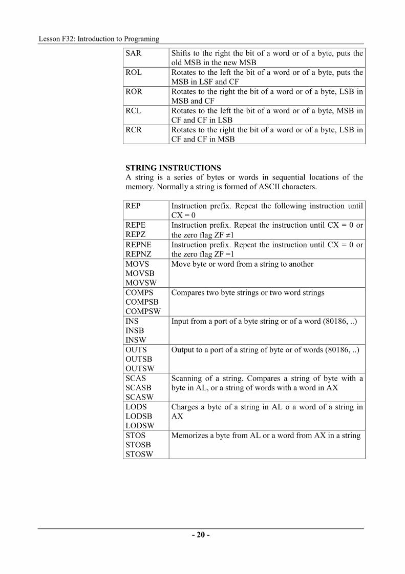
STRING INSTRUCTIONSA string is a series of bytes or words in sequential locations of thememory. Normally a string is formed of ASCII characters.
REP Instruction prefix. Repeat the following instruction untilCX = 0
REPEREPZ
Instruction prefix. Repeat the instruction until CX = 0 orthe zero flag ZF ≠1
REPNEREPNZ
Instruction prefix. Repeat the instruction until CX = 0 orthe zero flag ZF =1
MOVSMOVSBMOVSW
Move byte or word from a string to another
COMPSCOMPSBCOMPSW
Compares two byte strings or two word strings
INSINSBINSW
Input from a port of a byte string or of a word (80186, ..)
OUTSOUTSBOUTSW
Output to a port of a string of byte or of words (80186, ..)
SCASSCASBSCASW
Scanning of a string. Compares a string of byte with abyte in AL, or a string of words with a word in AX
LODSLODSBLODSW
Charges a byte of a string in AL o a word of a string inAX
STOSSTOSBSTOSW
Memorizes a byte from AL or a word from AX in a string

Lesson F32: Introduction to Programing
- 21 -
SKIPPING INSTRUCTIONS and CALL
CALL Calls a subprogram, saves the return address on the stackRET Returns from a subprogram to the calling programJMP Jumps all specified address to follow the next instructionJA/JNBE Jumps if above/Jumps if not below or equalJAE/JNB Jumps if above or equal/Jumps if not underJBE/JNA Jumps if below or equal /Jumps if not belowJC Jumps if Carry Flag CF=1JE/JZ Jumps if equal/Jumps if Zero Flag ZF=1JG/JNLE Jumps if more than/Jumps if not less or equalJGE/JNL Jumps if more than or equal /Jumps if not lessJL/JNGE Jumps if less/Jumps if not more than or equalJLE/JNG Jumps if less or equal/Jumps if not more thanJNC Jumps if no Carry Flag (CF=0)JNE/JNZ Jumps if not equal/Jumps if not zero (ZF ≠1)JNO Jumps if no overflow (overflow flag OF=0)JNP/JPO Jumps if no parity/Jumps if parity odd (PF=0)JNS Jumps if not sign (flag of sign SF=0)JO Jumps if flag overflow OF=1JP/JPE Jumps if parity/Jumps if parity even (PF = 1)JS Jumps if sign (SF=1)LOOP Follows a sequence of instructions until CX=0LOOPELOOPZ
Follows a sequence of instructions while ZF=1 e CX ≠ 0
LOOPNELOOPNZ
Follows a sequence of instructions while ZF=0 e CX ≠ 0
JCXZ Jumps to the specified address if CX=0INT Interrupts the execution of the program and calls a service
procedureINTO Interrupts the execution of the program if OF = 1IRET Returns from an interruption service
CONTROL INSTRUCTIONS of the PROCESSOR
STC Sets the carry flag CF = 1CLC Resets the carry flag CF = 0CMC Complements the state of the carry flagSTD Sets the direction flag DF = 1CLD Resets the direction flag DF = 0STI Sets the enabling flag of the interrupts at 1CLI Resets the enabling flag of the interruptsHLT Stops the processor until the arrival of an interruptWAIT Waits until the signal on pin TEST becomes lowESC Escapes from the external coprocessor (8087 or 8089)LOCK Instruction prefix. Blocks eventual external processorsNOP No operation

Lesson F32: Introduction to Programing
- 22 -
F32.7 SUMMARY QUESTIONNAIRE
���� Z3
���� SIS1
���� SIS2 Insert code Lesson: F32
Q1 The instruction: MOV AL,33H is an instruction of the microprocessorwritten in ? SETA B 1 3 Machine Language 2 1 Assembler Language 3 2 High level Language
Q2 Indicate which of the following doesn’t correspond to a possibledestination of an instruction of data movement MOV ? SETA B 1 2 A number 2 3 A register 3 1 A memory site
Q3 Which of the following is the data source in the immediateADDRESSING MODE? SETA B 1 2 A number 2 3 A register 3 1 A memory site

Lesson F32: Introduction to Programing
- 23 -
Q4 What does the expression [1024H] in the ADDRESSING MODE direct
into memory ( instruction MOV AL,[1024H] ) indicate? SETA B 1 4 The effective address of the site from where to take data 2 3 The absolute address of the site from where to take data 3 1 The contents of the site to the effective address 1024H 4 2 The shift with respect the Data Segment DS.
Q5 From which memory physical address is taken the data after theexecution of the instruction MOV AL,0410H, considering that thepresent contents DS is 1200 ? SETA B 1 2 1610H 2 3 0530H 3 4 0410H 4 1 12410H
Q6 Which of the following doesn’t identify an instructions group of themicroprocessor? SETA B 1 6 Data transferring instructions 2 4 Arithmetic instructions 3 5 Instructions for handling of bit 4 3 Research instructions 5 2 Skip and call instructions 6 1 Control Instructions of the processor
Lesson F33: Programing in Machine Code
- 24 -
LESSON F33: PROGRAMMING IN CODE MACHINE
OBJECTIVES• The models of the instructions• Codification of a simple instruction• Codification examples of different instructions MOV• Codification of a complete program
MATERIALS
• Base unit for the IPES system (power supply mod.PS1-PSU/EV,module holder mod.MU/EV, individual management unitmod.SIS1/SIS2/SIS3)
• Experimentation module mod. Z3/EV This lesson teaches how to construct the binary codes for themicroprocessor instructions. An assembler program normally carries out this codification operation,nevertheless, it is important to understand the principles in order to beable to develop immediate programs for Module Z3.
F33.1 THE MODELS of the INSTRUCTIONS
For the microprocessors equipped with few instructions the codificationin machine code is done using a table where all the instructionsindicated, with different addressing modes and the correspondingcodification. In the case of the microprocessors Intel x86 the number of theinstructions and of the variants of different addressing modes resultsequal to thousands and thus is impossible to indicate them in a table. Therefore, Models are used for each of the base instructions and bitfields are filled up in the models to specify the ADDRESSING MODE,types of data, etc. . See in appendix B the set of instructions of the microprocessor 386 withthe models used for each base instruction.
Lesson F33: Programing in Machine Code
- 25 -
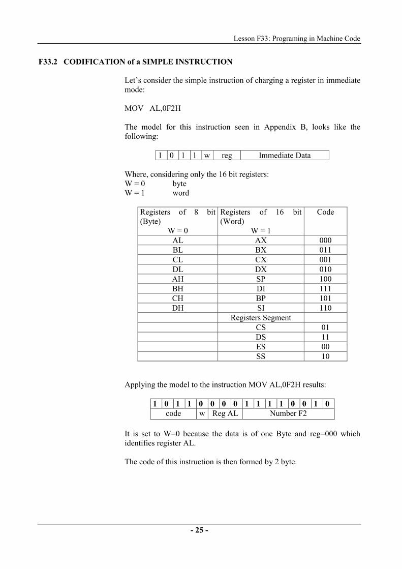
F33.2 CODIFICATION of a SIMPLE INSTRUCTION
Let’s consider the simple instruction of charging a register in immediatemode: MOV AL,0F2H The model for this instruction seen in Appendix B, looks like thefollowing:
1 0 1 1 w reg Immediate Data Where, considering only the 16 bit registers: W = 0 byte W = 1 word
Registers of 8 bit(Byte)
W = 0
Registers of 16 bit(Word)
W = 1
Code
AL AX 000 BL BX 011 CL CX 001 DL DX 010 AH SP 100 BH DI 111 CH BP 101 DH SI 110
Registers Segment CS 01 DS 11 ES 00 SS 10
Applying the model to the instruction MOV AL,0F2H results:
1 0 1 1 0 0 0 0 1 1 1 1 0 0 1 0 code w Reg AL Number F2
It is set to W=0 because the data is of one Byte and reg=000 whichidentifies register AL. The code of this instruction is then formed by 2 byte.
Lesson F33: Programing in Machine Code
- 26 -
F33.3 EXAMPLES of CODIFICATION of the DIFFERENT INSTRUCTIONS MOV
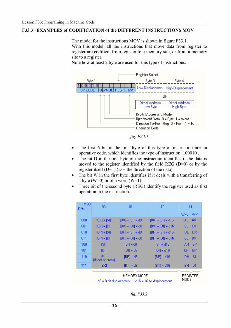
The model for the instructions MOV is shown in figure F33.1. With this model, all the instructions that move data from register toregister are codified, from register to a memory site, or from a memorysite to a register. Note how at least 2 byte are used for this type of instructions.
fig. F33.1
• The first 6 bit in the first byte of this type of instruction are an
operative code, which identifies the type of instruction: 100010 .• The bit D in the first byte of the instruction identifies if the data is
moved to the register identified by the field REG (D=0) or by theregister itself (D=1) (D = the direction of the data).
• The bit W in the first byte identifies if it deals with a transferring ofa byte (W=0) or of a word (W=1).
• Three bit of the second byte (REG) identify the register used as firstoperation in the instruction.
fig. F33.2

Lesson F33: Programing in Machine Code
- 27 -
The two bits (MOD) and the three bits (R/M) in the second byte of theinstruction are used to specify the ADDRESSING MODE of the secondoperation of the instruction. Figure F33.2 shows the table with the combinations of MOD and R/Mfor each of the 32 possible addressing modes. It can be noted that:• If the other operation of the instruction is also a register, then it is
enough to put 11 in the bit MOD and the code of the register at 3 bitin R/M.
• If the other operation of the instruction is a memory site, there are24 modes to specify the effective address of the operation inmemory.• The bit of the field MOD are used to indicate if address contains
a shift (displacement) or not, while the field R/M encodes theregister(s) that contain the effective address.
• Use MOD=00 if the address does not contain any shifts. Forexample for the instruction MOV AX,[SI] it’s necessary to putMOD=00 e R/M=100. In the case of direct addressing MOVAX,[124FH] it’s necessary to put MOD=00, R/M=110, the byteLSB of the address in the third byte of the instruction and thebyte MSB of the address in the fourth byte of the instruction.
• Use MOD=01 if the address of the instruction contains a shiftless than 256. For example in the case of the instruction MOVAX,12H[BX] it’s necessary to put MOD=01, R/M=111 and theshift 12H is put in the third byte of the instruction.
• Use MOD=10 if the address of the instruction contains a shiftgreater than 256. For example in the case of the instructionMOV AX,2A12H[BX] it’s necessary to put MOD=10, R/M=111and the shift 2A12H is put in the third and fourth byte of theinstruction (12H in the third and 2AH in the fourth).
Let’s see now some examples of instruction codification MOV.
Lesson F33: Programing in Machine Code
- 28 -
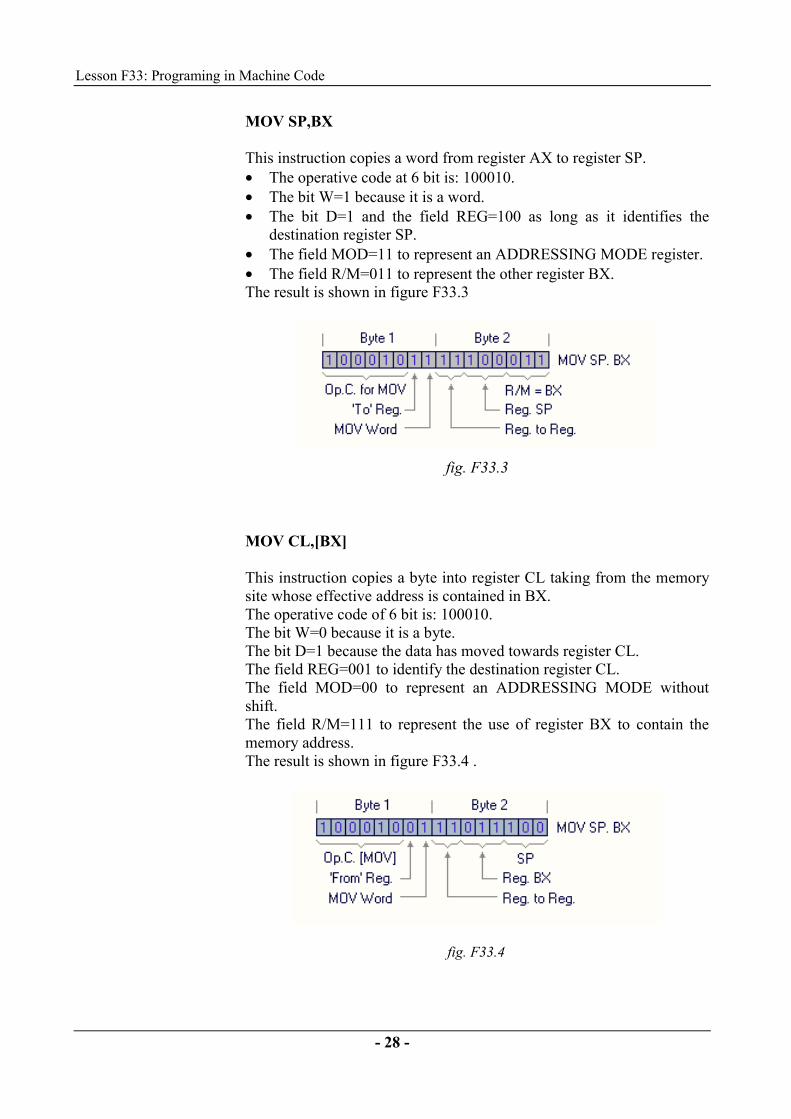
MOV SP,BX
This instruction copies a word from register AX to register SP.• The operative code at 6 bit is: 100010.• The bit W=1 because it is a word.• The bit D=1 and the field REG=100 as long as it identifies the
destination register SP.• The field MOD=11 to represent an ADDRESSING MODE register.• The field R/M=011 to represent the other register BX.The result is shown in figure F33.3
fig. F33.3
MOV CL,[BX]
This instruction copies a byte into register CL taking from the memorysite whose effective address is contained in BX.The operative code of 6 bit is: 100010.The bit W=0 because it is a byte.The bit D=1 because the data has moved towards register CL.The field REG=001 to identify the destination register CL.The field MOD=00 to represent an ADDRESSING MODE withoutshift.The field R/M=111 to represent the use of register BX to contain thememory address.The result is shown in figure F33.4 .
fig. F33.4
Lesson F33: Programing in Machine Code
- 29 -
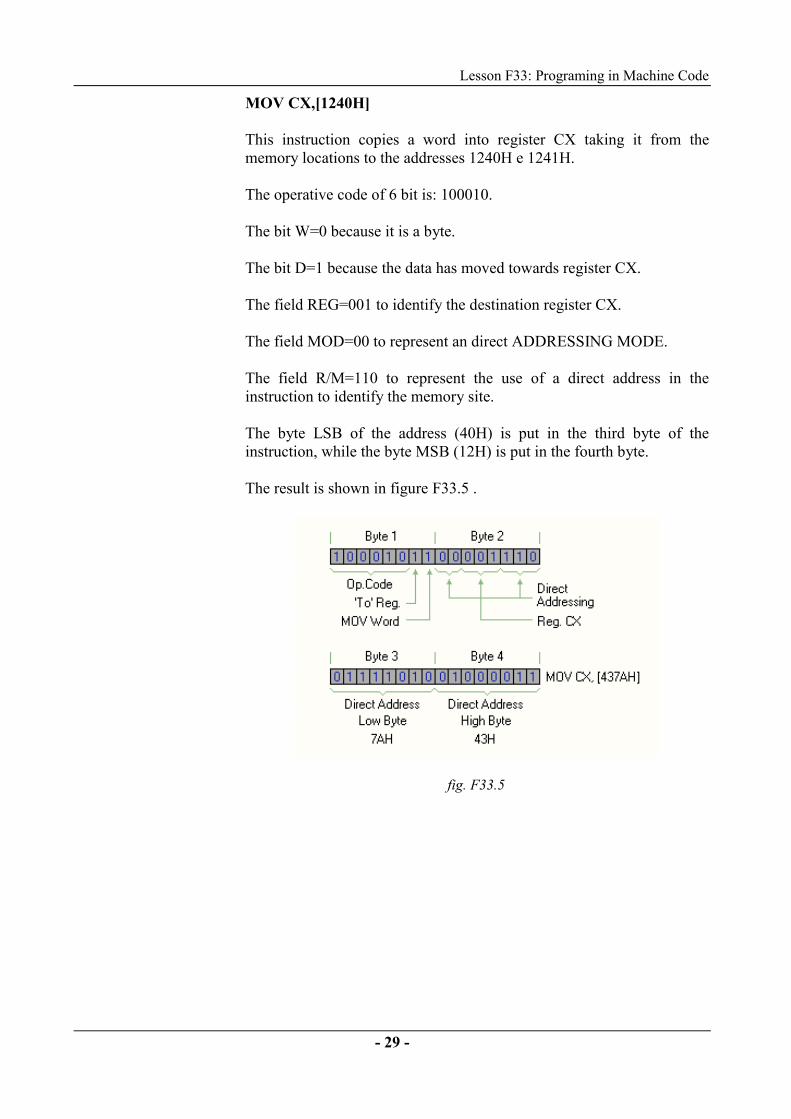
MOV CX,[1240H]
This instruction copies a word into register CX taking it from thememory locations to the addresses 1240H e 1241H.
The operative code of 6 bit is: 100010.
The bit W=0 because it is a byte.
The bit D=1 because the data has moved towards register CX.
The field REG=001 to identify the destination register CX.
The field MOD=00 to represent an direct ADDRESSING MODE.
The field R/M=110 to represent the use of a direct address in theinstruction to identify the memory site.
The byte LSB of the address (40H) is put in the third byte of theinstruction, while the byte MSB (12H) is put in the fourth byte.
The result is shown in figure F33.5 .
fig. F33.5

Lesson F33: Programing in Machine Code
- 30 -
MOV CS:[BX],DL
This instruction copies a byte from register DL into a memory site.
The effective address of the site is contained in BX.
Normally the effective address is added to the segment data DS to formthe physical address of the memory. In this case the notation CS:[BX]indicates that register CS is to be used instead of DS.
The notation CS: is called segment override prefix.
When an instruction contains a segment override prefix it’s necessary toput a code of 8 bit before the rest of the instruction. This code has theformat 001XX110 where XX represents the code of the register segmentused.
In our case CS=01 and the segment override prefix becomes 00101110.The remaining codification respects the procedures seen beforehand.
The result is shown in figure F33.6 .
fig. F33.6
Lesson F33: Programing in Machine Code
- 31 -
F33.4 SUMMARY QUESTIONNAIRE
���� Z3
���� SIS1
���� SIS2 Insert code Lesson: F33
We want to encode in machine language the following program:
Program PRG_01 Label Instruction Comment START: MOV DX,0310H Immediate charging instruction of a register of
16 bit.Charges in register DX the address of the portA of the parallel interface
MOV AL,55H Immediate charging instruction of a register of8 bit.Charges in register AL the data to be sent onthe port
OUT DX,AL Output instruction data on an I/O variableport. Sends the data on the output port
INT 07H Interrupt software.Calls the interrupt 07H that causes the returnof the control to the Monitor of the system
This program can be used directly on Module Z3/EV. It sends on Port A of the parallel interface of the module (connector J1)the number 55H (01010101B). For its use it’s necessary first of all to transform the instructions inmachine code. The tables of the appendix are to be used.
Q1 Which of the following expressions codifies in correct mode theinstruction MOV DX,0310H (Table E-1, Sheet 1)? SETA B 1 4 10111010 2 3 10111010 00010000 00000011 3 5 10111110 00010000 00000011 4 2 10111110 00000011 00010000 5 1 10111010 00000011 00010000

Lesson F33: Programing in Machine Code
- 32 -
Q2 Which of the following expressions codifies in correct mode the
instruction MOV AL,55H (Table E-1, Sheet 1)? SETA B 1 4 10110000 010101012 3 10111000 01010101 3 2 01010101 4 1 10110000 00000000 01010101
Q3 Which of the following expressions codifies in correct mode theinstruction OUT DX,AL (Table E-1, Sheet 2) ? SETA B 1 3 11100110 00010000 000000112 4 11101111 3 2 11101110 4 1 11101110 0110000
Q4 Which of the following expressions codifies in correct mode the
instruction INT 07H (Table E-1, Sheet 14) ? SETA B 1 2 11001101 000001112 4 11001100 3 1 11001101 4 3 00000111 11001101
Lesson F34: Programing in Assembler Language
- 33 -
LESSON F34: PROGRAMMING in ASSEMBLER LANGUAGE
OBJECTIVES• Format of a program in assembler language• Types of numbers used• The instructions of the assembler• The working phases: assembler, linker, ..• Creation of simple programs
MATERIALS
• Base unit for the IPES system (power supply mod.PS1-PSU/EV,module holder mod.MU/EV, individual management unitmod.SIS1/SIS2/SIS3)
• Experimentation module mod. Z3/EV This lesson teaches how to construct programs for the System with 32bit Microprocessor using the assembler language. This language eliminates the tedious job of the transformation of theinstructions in machine code seen on the preceding lesson. There are different assembler languages available in the market. All theexamples in this manual will refer to the assembler MASM of theMicrosoft Corp. .
F34.1 FORMAT of a PROGRAM in ASSEMBLER LANGUAGE
To illustrate the format of a program in assembler language let’s refer tothe simple example PRG_05 indicated next. This program consists of adding two numbers present in 2 memorylocations and putting the result in a third site. The following characteristics can soon be noted: • The characters that are preceded by the sign ‘;’ are considered as
comments (it’s a good norm to add comments in the interior of aprogram in order to render it more legible).
• The instructions respect the syntax of the instructions of the
microprocessors Intel series x86 seen in the precedent lessons. • Besides the instructions, there are other character strings that have

lesson F34: Programing in Assembler Language
- 34 -
nothing to do with the instructions of the microprocessor, but servethe assembler; these are called ‘directives’.
• The numbers at the interior of the program can be written in
different forms: decimal (2, 45, ..), hexadecimal (12H, ..), etc. . All of these characteristics will be analyzed in the run of the lesson. ;----------------------------- PRG_05 ------------------------- ;this program sums two byte present in N.2 different memory locations ; and puts the result in a third ;memory site of 1 byte (supposing that the result does not exceed number 255) IMONITOR EQU 07H ;---------------------------------------- CODE ;the program is charged to the address 0200:0000H PROG SEGMENT ASSUME CS:PROG, DS:PROG START: MOV AX,0200H ;charges the register DS MOV DS,AX MOV AL,DATA_1 ;charges in AL the first data MOV BL,DATA_2 ;charges in BL the second data ADD AL,BL ;sums MOV ADDITION,AL INT IMONITOR ;returns to the monitor ;------------------------- data DATA_1 DB 04H ;first data (04H) DATA_2 DB 12H ;second data (12H) ADDITION DB 00000000B ;result PROG ENDS END START
F34.2 TYPES of NUMBERS USED
In the program are used different forms to represent data. The possibleforms are the following: BINARY Adding a B to the string of 1 and 0, which represents them, indicates thebinary numbers. Examples: 01010101B 111111110000000B DECIMAL The decimal numbers are specified without any special identificationsign. Examples: MOV AL,15 MOV AH,110
Lesson F34: Programing in Assembler Language
- 35 -
If a negative number is indicated, the assembler transforms it in thecorresponding notation in complement to 2. HEXADECIMAL The decimal numbers are indicated are indicated by adding an H to thehexadecimal notation. Examples: 24H 0A2H In the case in which the hexadecimal numbers start with a letter, it’snecessary to put a 0 before the starting letter. STRINGS of ASCII CHARACTERS It is possible to declare a sequence of characters ASCII (string) closingthe peaks of the string. Example DB ‘MOZ-Z3’ This instruction reserves 6 memory locations. In the first one, the ASCIIcode of the letter M is put, in the second one, that of the letter O, and soon.
F34.3 THE DIRECTIVES of the ASSEMBLER
The directives are used to provide the assembler with the informationabout how to behave during the transformation of the instructions inmachine code. There are many directives and for a complete analysis refer to themanuals used by the assembler. Next, the most important ones will be indicated and analyzed. Directives SEGMENT and ENDS These directives are used to identify a group of data or a group ofinstructions that we want to gather together in a certain segment. In the program under review is used a segment called PROG thatcontains either the program or the data. The directives are: PROG SEGMENT …………….. PROG ENDS
Directives EQU, DB,DW,DD In a program there are generally 3 categories of data: the constants, thevariables, the addresses. It is possible to assign names to the constants, variables and addresses inorder to make reference to them with a name, instead as with a number(this renders the programs more legible).

lesson F34: Programing in Assembler Language
- 36 -
The directive EQU is used to assign names to the constants of aprogram. Example: IMONITOR EQU 07H
During the assembling, the name IMONITOR will be substituted withinthe program by the constant number 07H. See how the instruction to return to the monitor (INT 07H) has beenwritten as INT IMONITOR. The directives DB, DW, DD are used to assign names to the variablesin a program. Example: DATA_1 DB 04H
The preceding syntax declares a variable of the byte type (DB), they areassigned the name DATA_1, and is initialized with the value 04H. Analyzing then the instruction: MOV AL,DATA_1
It’s seen how the present value of the variable can be accessed (which ischarged into register AL) directly by means of its name. DATA_1 is no more and no less than the memory address where thebyte is memorized. The assembler, with respect to the segment in whichthe variable is declared calculates this address,. The directives DW and DD are analog to the directive DB, only thatthey define variables of the Word type and Double Word respectively. DIRECTIVE ASSUME The directive ASSUME tells the assembler which logic segment it mustuse for each of the physical segments of the microprocessor (codesegment, data segment, stack segment, extra segment). In the example under consideration, the directive: ASSUME CS:PROG, DS:PROG
tells that the logic segment PROG has to be used as code segment andas data segment. All the addresses inherent to the code and the data will be Calculatedrespect to this segment. The directive ASSUME serves only as reference to the assembler, butdoesn’t change the value of the segment registers. it is thus the job ofthe programmer, that of charging the registers with the right values. The program in matter charges in fact, with the first two instructions,the data segment register DS with the appropriate values: START: MOV AX,0200H ;charges the register DS MOV DS,AX

Lesson F34: Programing in Assembler Language
- 37 -
Without these instructions the register DS wouldn’t be modified andthen the data would surely be taken by wrong memory locations. The register CS is charged at the time of the starting of the program. Directive END The directive END indicates the assembler that the program is finished. There are many other directives of the assembler, that very often are notgeneral, but specifically of the assembler that is being used. These directives will be illustrated in the following lessons, when theprograms that will be developed will request their insertion.
F34.4 THE WORKING PHASES for the CREATION of PROGRAMS in ASSEMBLER The creation of assembler programs for use in a system like the 32 BitMicroprocessor Trainer Mod. Z3/EV requires different working phases. These working phases, that remain the same for any system, areillustrated next, along with the instruments that are used in each one ofthem. The writing of the programs (Editor) An editor is a program that allows creating a file that contains theinstructions in assembler language corresponding to the program. Instruments like the Note Pad of Windows or video-writing programscan be used. When using Module Z3/EV, the integrated editor in the programMODZ3/EV is used. Assembling of the programs (Assembler) The program Assembler is used to transform the written instructions inassembler language, to the corresponding machine codes. The assembler reads the source file (.ASM) that contains the programand generates 2 files:• (.OBJ) contains the binary codes of the instructions and the
information referring to the addresses of the instructions,• (.LST) contains the complete list of the instructions and generated
codes. Linker The linker is a program used to put together different OBJ file in asingle file. The generated file of the linker has extension .EXE. It can be directlyused under control of the operative system MS-DOS that considers acharge in memory, by assigning the positioning addresses into thememory in a correct way.
lesson F34: Programing in Assembler Language
- 38 -
In case of use with systems type, the Module Z3/EV has to beappropriately modified by a program that transforms it in binary mode. Transformation in pure binary code (EXE2BIN) The operative system MS-DOS contains a program that transforms a file.EXE in a pure binary file that contains only the program codes. This program is called EXE2BIN. It transforms the file .EXE in a file .BIN that contains only the binarycodes. Charging of the program into Module Z3/EV (MODZ3) the program MODZ3, issued with module Z3/EV, considers thetransfer of the program from file .BIN to the RAM memory of moduleZ3, where it should be followed afterwards. This transfer can be doneby means of the serial interface or the parallel interface. Verification of the functioning of the program (Debugging) The verification of the functioning of the program is done directly inmodule Z3/EV. During this phase, called debugging, the continuous executioncommands are used, step-step execution, breakpoints introduction,display of the registers and of the memory, of System Z3/EV. All of these phases will be reviewed in the following lessons that willbe object of program development for module Z3/EV.

Lesson F34: Programing in Assembler Language
- 39 -
F34.5 SUMMARY QUESTIONNAIRE
���� Z3
���� SIS1
���� SIS2 Insert code Lesson: F34
We would like to develop a program, similar to that seen in the theorypart of this lesson, that:• uses two different segments for the code and for the data• sums two word of value 0120H and 0241H respectively• puts the result in a third word in the memory. The trace of the program is shown next. The following questions refer to the instructions and directives ofincomplete programs or missing ones. ;----------------------------- PRG_07 ------------------------- ;this program sums two words present in memory, ;of value 0120H and puts the result in a third word in the memory (it is suppose that the result ;does not exceed 16 bit) IMONITOR EQU 07H DS_SEG 0080H ;---------------------------------------- DATA DATA xxxxxxxxxxxx DATA_1 xxxxxxxxxxxx DATA_2 xxxxxxxxxxxx xxxxxxxx ENDS ;---------------------------------------- CODE ;the program is charged to the address 0200:0000H PROG SEGMENT ASSUME xxxxxxxxxxxxxxxxxxx START: MOV AX,xxxxx ;charges DS with data segment MOV DS,AX MOV xx,DATA_1 ;charges the first data MOV BX,DATA_2 ;charges the second data ADD AX,BX ;sums MOV SUMS,AX INT IMONITOR ;returns to the monitor PROG ENDS END START
lesson F34: Programing in Assembler Language
- 40 -
Q1 Which of the following expressions have to be substituted to xxxxxxxxxxof the line: DATA xxxxxxxxxx ? SETA B 1 2 ASSUME 2 5 SEGMENT 3 4 ENDS 4 1 0120H 5 2 0241H
Q2 Which of the following expressions have to be substituted to xxxxxxxxxxof the line: DATA_1 xxxxxxxxxx ? SETA B 1 5 ASSUME 2 1 DD 0120H 3 4 DB 0120H 4 2 DW 0120H 5 3 0120H
Q3 Which of the following expressions have to be substituted to xxxxxxxxxxof the line: DATA_2 xxxxxxxxxx? SETA B 1 4 ASSUME 2 1 DW 0120H 3 5 DW 0241H 4 3 DD 0120H 5 2 DD 0241H
Q4 Which of the following expressions have to be substituted to xxxxxxxxxx
of the line: xxxxxxxx ENDS ? SETA B 1 2 ASSUME 2 5 SEGMENT 3 4 ENDS 4 3 DATA 5 1 0241H

Lesson F34: Programing in Assembler Language
- 41 -
Q5 Which of the following expressions have to be substituted to xxxxxxxxxx
of the line: ASSUME xxxxxxxxxxxxxxxxxxxxxxx ? SETA B 1 4 CS:PROG, DS:PROG 2 5 DS:PROG, CS:PROG 3 1 CS:PROG, DS:DATA 4 2 CS:PROG 5 3 DS:DATA
Q6 Which of the following expressions have to be substituted to xxxxxxxxxxof the line: MOV AX,xxxxx ? SETA B 1 4 0120H 2 5 0000H 3 1 PROG 4 3 DS:DATA 5 2 DS_SEG
Q7 Which of the following expressions have to be substituted to xx of theline: MOV xx,DATA_1 ? SETA B 1 3 AL 2 1 AH 3 4 AX 4 5 DX 5 2 DS
lesson F35: The microprocessor of 32 Bit 80386
- 42 -
LESSON F35: THE MICROPROCESSOR of 32 BIT 80386
OBJECTIVES• Evolution from 8086 to the 80386• Internal structure of the 386• The registers• The set of the instructions• The functioning modes
MATERIALS
• Base unit for the IPES system (power supply mod.PS1-PSU/EV,module holder mod.MU/EV, individual management unitmod.SIS1/SIS2/SIS3)
• Experimentation module mod. Z3/EV In this lesson the microprocessor 80386 is illustrated. Until now, the 8086 has been used because it is the simplest member ofthe Intel microprocessors family, and thus the best starting point. The microprocessor 80386 results compatible with the 8086 andincreases the potentiality with its 32-bit structure.
F35.1 EVOLUTION from 8086 to 386
The successive microprocessor to the 8086, leaving aside 186, is the80286. It is an upgrade of 16 bit of the 8086, provided even with managementcircuits of the virtual memory, protection circuits, and with thepossibility of addressing 16 MB of memory. It is the first micro of thefamily projected for use in multi-user or multi-task systems. The 80386 is a microprocessor of 32 bit with bus of the addresses of 32bit. The ALU of 32 bit allows the 386 to elaborate the data faster, while theaddressing of 32 bit allows addressing up to 4GB of memory. It is particularly indicated for use with operative multi-task systems; infact, its internal memory management and protection circuits have beenupgraded. Additionally, the 386 allows following contemporaneously severaloperative systems.

Lesson F35: The microprocessor of 32 Bit 80386
- 43 -
F35.2 The INTERNAL STRUCTURE
The internal block diagram of the microprocessor 80386 is shown infigure F35.1.
fig. F35.1 The 80386 is formed of a Central Processing Unit, of a MemoryManagement Unit and of a Bus Interface Unit. The Central Processing Unit is formed of the Execution Unit and of theInstruction Unit. The Execution Unit contains the 8 registers of 32 bit for general use,together with the ALU. The Instruction Unit decodes the instructions operative codes and savesthem in a queue for immediate use by the Execution Unit. The Memory Management Unit (MMU) consists of a segmentation unitand of an editing one. The memory is organized in one or moresegments, each of which being able to arrive up to 4 GB. Thesegmentation unit is provided with 4 protection levels to isolate andprotect the applications from each other. The Interface Unit provides the connection signals of themicroprocessor with the external peripherals: memory, devices, I/O, .. . The 80386 has two main functioning modes:• Real Mode: the 386 operates as a faster 8086, with the extensions at
32 bit.• Protected Mode: the 386 provides a sophisticated memory
management system to allow the multi-task operation.

lesson F35: The microprocessor of 32 Bit 80386
- 44 -
In the 32 Bit Microprocessor Trainer the Real Mode is used.Everything referring the Protected Mode and thus it will not be seenin depth from now on.
F35.3 THE REGISTERS The 80386 has 32 registers altogether, divided in the following categories:
• Registers of general use• Segment registers• Instructions pointers and register of the Flags• Control registers• System addressing registers• Debug registers• Test registers. These registers are a superset of registers of the 8086, in such way thatall the registers of the 8086 are included in the 386. Figure 35.2 shows the base architecture of the registers of the 386,divided in:• general data and address registers• segments selectors registers• Instructions pointers and register of the Flags
fig. F35.2

Lesson F35: The microprocessor of 32 Bit 80386
- 45 -
Registers of general use The 8 registers of general use at 32 bit can memorize data or addresses.These registers, figure F35.3, support operands of 1, 8, 16, 32 and 64bits, and bit field from 1 to 32. They support additionally addresses of16 or 32 bit. The registers are called: EAX, EBX, ECX, ESI, EDI, EBP and ESP.
fig. F35.3
It’s possible to access to the least significant 16 bit of the registers. Thisis done using the nominatives: AX, BX, CX, DX, SI, DI, BP and SP.When accessing to the registers of 16 bit, the superior parts aren’t eitherused or changed. In the end, operations at 8 bit can access separately the least significantbyte (bits 0-7) and the most significant byte (bits 8-15) of the registersAX, BX, CX and DX. the least significant byte are called AL, BL, CLand DL, while the most significant are called AH, BH, CH and DH.
Instruction Pointer The instruction pointer is a register of 32 bit called EIP. It contains theoffset of the next instruction that has to be followed. This offset isalways referred to the segment code register CS. The inferior part of 16 bit (bits 0-15) of EIP contains instructionspointer IP, that is used in the 16 bit addressing.
Flags Register The flags register is a register of 32 bit called EFLAGS. The meaning ofthe bits in contained in it is shown in figure F35.4. The inferior part of 16 bit (bits 0-15) of EFLAGS contains the registerof 16 bits FLAGS used when 8086 compatible instructions arefollowed.
lesson F35: The microprocessor of 32 Bit 80386
- 46 -
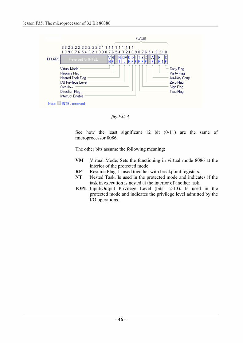
fig. F35.4
See how the least significant 12 bit (0-11) are the same ofmicroprocessor 8086. The other bits assume the following meaning: VM Virtual Mode. Sets the functioning in virtual mode 8086 at the
interior of the protected mode.RF Resume Flag. Is used together with breakpoint registers.NT Nested Task. Is used in the protected mode and indicates if the
task in execution is nested at the interior of another task.IOPL Input/Output Privilege Level (bits 12-13). Is used in the
protected mode and indicates the privilege level admitted by theI/O operations.
Lesson F35: The microprocessor of 32 Bit 80386
- 47 -
Segment Registers
The 6 segment register of 16 bit contain the segments values in thememory, corresponding to: code: register CS stack: register SS data: registers DS, ES, FS, GS. In the protected mode, each segment can change in amplitude from onebyte up to the entire addressing space of the micro, 4 GB (2^32 bytes). In the real mode, the maximum amplitude of a segment is of 64KB(2^16 bytes).
Segment Description Registers The Segment Description Registers are not visible to the programmer.They are associated to each of the segment registers and contain a baseaddress of 32 bit and a segment limit also of 32 bit. This renders possible the management of segments of amplitude up to a4GB using segment registers of 16 bit.
Control Registers The 80386 has 3 control registers of 32 bit: CR0, CR1 and CR2, whichcontain the complete microprocessor’s state. They are used in theprotected mode and will not be analyzed here.
System Address Registers 4 specific registers are used for the management of tables/segments usedin the protection model of the protected mode: GDT Global Descriptor Table IDT Interrupt Descriptor Table LDT Local Descriptor Table TSS Task State Segment. These registers too, being specific of the protected mode, will not beanalyzed.
Test and Debug Registers The 80386 uses 6 debug registers and 3 test registers for specifictest/debug operations that will not be analyzed.

lesson F35: The microprocessor of 32 Bit 80386
- 48 -
F35.4 THE SET of INSTRUCTIONS
The complete set of the instructions of the 80386 is divided in 9categories:• Data transfer• Arithmetic• Rotation/Shift• String manipulation• Bit manipulation• Control transfer• Support of high level language• Support of the operative system• Control of the processor. All the instructions operate on 0, 1, 2 o 3 operands; where an operandcan reside in a register, in the instruction itself, or in the memory. The operands can be 8, 16 o 32 bytes long. As general rule, when thewritten code for the 80386 is followed (code a 32 bit) the operands are 8or 32 bits long. When the code for the 8086 is followed (code a 32 bit) the operands are8 or 16 bits long. To modify the default lengths, prefixes can be added to all theinstructions. The average instruction is 3.2 bytes long. Because the 80386 has aninstructions queue of 16 bytes, about 5 instructions reside in this queuealready decoded Next a table with the summary of all the 80386instructions is shown.Compare this table with that analog for the 8086 of lesson F32. INSTRUCTIONS of DATA TRANSFER
GENERAL USEMOV Moves an operandPUSH Copies an operand on the stackPOP Picks an operando from the stackPUSHA Copies all registers on the stackPOPA Picks all registers from the stackXCHG Exchanges operands, registersXLAT Transforms the operand
CONVERSIONMOVZX Moves Byte, Word, Dword with zero extensionMOVSX Moves Byte, Word, Dword with sign extensionCBW Converts Byte to Word, or Word to DwordCWD Converts Word to DwordCWDE Converts Word to Dword itselfCDQ Converts Dword to Qword
Lesson F35: The microprocessor of 32 Bit 80386
- 49 -
INPUT/OUTPUTIN Input of an operand from the I/O spaceOUT Output of an operand on the I/O space
ADDRESSLEA Charges effective addressLDS Charges a pointer into register DSLES Charges a pointer into register ESLFS Charges a pointer into register FSLGS Charges a pointer into register GSLSS Charges a pointer into segment register of the stack
MANIPULATION of the FLAGSLAHF Charges the register A from the FlagsSAHF Memorizes the register A in the flagsPUSHF Copies the flags register on the stackPOPF Picks from stack the flags registerPUSHFD Copies the register EFLAGS on the stackPOPFD Picks the register EFLAGS from the stackCLC Resets the carry flagCLD Resets the direction flagCMC Completes the carry flagSTC Sets to 1 the carry flagSTD Sets to 1 the direction flag
INSTRUCTIONS ARITHMETIC
ADDITIONADD Adds operandsADC Adds with carryINC Increments the operand of 1AAA Adjusting ASCII for the additionDAA Adjusting decimal for the addition
SUBTRACTIONSUB Subtracts operandsSBB Subtracts considering also the value of the carry flagDEC Decrements operand of 1NEG Denies operandCMP Compares operandsAAS Adjusting ASCII after a subtractionDAS Adjusting decimal after a subtraction
MULTIPLICATIONMUL Multiplication in double/single precisionIMUL Multiplication (entire)AAM Adjusting ASCII after multiplication
DIVISIONDIV Division without signIDIV Division (entire)AAD Adjusting ASCII before the division
lesson F35: The microprocessor of 32 Bit 80386
- 50 -
STRING INSTRUCTIONSMOVS Moves Byte strings, Word or DwordINS Input of an I/O port of a stringOUTS Output of an I/O port of actionsCOMPS Compares two Byte strings, Word or DwordSCAS Scanning of a Byte string , Word or DwordLODS Charge of a Byte stringe, Word or DwordSTOS Memorization of a Byte stringe, Word or DwordREP RepetitionREPEREPZ
Repeats the instruction until CX=0 or the zero flag ZF ≠1
REPNEREPNZ
Repeats the instruction until CX=0 or the zero flag ZF =1
LOGIC INSTRUCTIONSLOGIC
NOT ‘NOT’ of the operandsAND ‘AND’ of the operandsOR ‘OR inclusive’ of the operandsXOR ‘OR exclusive’ of the operandsTEST ‘Test’ of the operands
SHIFTSHL/SHR Logic shift to left or rightSAL/SAR Arithmetic shift to left or rightSHLD/SHRD
Double shift to left or right
ROTATIONROL/ROR Rotation to left or rightRCL/RCR Rotation to left or right with carry
BIT MANIPULATION INSTRUCTIONSINSTRUCTIONS OF SINGLE BIT
BT Bit testBTS Bit test and setBTR Bit test and resetBTC Bit test and completementBSF Straight bit scanningBSR Inverse bit scanning

Lesson F35: The microprocessor of 32 Bit 80386
- 51 -
PROGRAM CONTROL INSTRUCTIONS
CONDITIONED TRANSFERSETCC Sets a byte equal to the condition codeJA/JNBE Jumps if above/Jumps if not below or equalJAE/JNB Jumps if above or equal/Jumps if not belowJB/JNAE Jumps if below/neither above nor equalJBE/JNA Jumps if below or equal/Jumps if not aboveJC Jumps if Carry Flag CF=1JE/JZ Jumps if equal/Jumps if Zero Flag ZF=1JG/JNLE Jumps if greater than/Jumps if not less or equalJGE/JNL Jumps if greater than or equal/Jumps if not lessJL/JNGE Jumps if less/Jumps if not greater than or equalJLE/JNG Jumps if less or equal/Jumps if not greater thanJNC Jumps if no Carry Flag (CF=0)JNE/JNZ Jumps if not equal/Jumps if not zero (ZF ≠1)JNO Jumps if no overflow (overflow flag OF=0)JNP/JPO Jumps if no parity/Jumps if odd parity (PF=0)JNS Jumps if no sign (flag di sign SF=0)JO Jumps if flag overflow OF=1JP/JPE Jumps if parity/Jumps if even parity (PF = 1)JS Jumps if sign (SF=1)
UNCONDITIONED TRANSFERCALL Procedure call or taskRET Return from procedureJMP Jump
INTERACTION CONTROLLOOP Follows a sequence of instructions until CX=0LOOPELOOPZ
Follows a sequence of instructions while ZF=1 and CX ≠0
LOOPNELOOPNZ
Follows a sequence of instructions while ZF=0 and CX ≠0
JCXZ Jumps to the specified address if CX=0INTERRUPTION
INT InterruptionINTO Interrupts the execution of the program if OF = 1IRET Returns from an interruption serviceCLI Disables interruptionsSTI Enables interruptions
HIGH LEVEL LANGUAGE INSTRUCTIONSBOUND Verifiies the limits of an arrayENTER Sets parametrers block for a procedureLEAVE Leaves of a procedure

lesson F35: The microprocessor of 32 Bit 80386
- 52 -
PROTECTED MODE INSTRUCTIONSSGDT Memorizes Global Descriptor TableSIDT Memorizes Interrupt Descriptor TableSTR Memorizes Task RegisterSLDT Memorizes Local Descriptor TableLGDT Charges Global Descriptor TableLIDT Charges Interrupt Descriptor TableLTR Charges Task RegisterLLDT Charges Local Descriptor TableARPL Aggiusta Rethesed Privilege LevelLAR Charges Access RightsLSL Charges Segment LimitVERR/VERW
Verifies segment for reading or writing
LMSW Charges Machine Status WordSMSW Memorizes Machine Status Word PROCESSOR CONTROL INSTRUCTIONSHLT HaltWAIT Wait until BUSY# deniedESC EscapeLOCK Lock of Bus
F35.5 ADDRESSING of 16 and 32 BIT
In order to furnish the software compatibility with the 8086, the 80386can follow instructions of 16 bit in the Real and Protected Modes. The microprocessor determines the magnitude of the instruction that isfollowing the examination of bit D of the segment CS descriptor. If bitD is at 0, then the addressings are considered of 16 bit, conversely, if bitD is at 1, the addressings are considered of 32 bit. In the Real mode it’s assumed by default the addressing of 16 bit. Independently of the magnitude of the operands or of the addresses, the80386 is able to follow be it the instructions at 16 or at 32 bit. This isdone by means of the use of a prefix in the instruction. Two prefixes, the Operand Size Prefix and the Address Length Prefix,are used for this finality. The prefixes are automatically inserted in the code of the Assemblerprogram being used.
F35.6 FUNCTIONING IN REAL MODE
When the 8086 is powered on, or after a reset, it is predisposed in theReal mode. The Real mode has the same base functioning of the 8086, but allows

Lesson F35: The microprocessor of 32 Bit 80386
- 53 -
the access to the registers of 32 bit of the 386. The ADDRESSINGMODE, the amplitude of the memory, the management of theinterruptions, are identical to the 8086. All the instructions, with the exception of those in the Protected mode,are available. The default amplitude of the operands is of 16 bit. In order to use the registers and addresses of 16 bit, the instructionprefixes have to be used. The maximum amplitude of a segment is of 64KB. The maximum memory amplitude is of 1 MB, in this way, lines A2-A19are active. There are two areas of fixed memory reserved in the real mode: the locations from 00000H to 003FFH are reserved for the interruptionvectors. The locations from FFFFFFFF0H to FFFFFFFFFH are reserved for theinitialization.
F35.7 FUNCTIONING IN PROTECTED MODE
The complete performance of the 80386 is available when it works inthe Protected mode. This mode increments greatly the memory space up to 4 GB (32 bit) andallows the execution of virtual programs in memory of any amplitude. Allows also the execution of software 8086, with a sophisticatedmemory management and its protection. The Protected mode provides additional instructions, which areparticularly indicated, for supporting multi-task operative systems. The Protected mode is not analyzed here, due to the limited memoryresources of Module Z3/EV, and to its complexity.
lesson F35: The microprocessor of 32 Bit 80386
- 54 -
F35.8 SUMMARY QUESTIONNAIRE
���� Z3
���� SIS1
���� SIS2 Insert code Lesson: F35
Q1 Which of the following expressions, referring the microprocessor 80386is not true ? SETA B 1 2 The addresses bus is of 32 bit 2 1 The data bus is of 32 bit 3 5 The internal registers are of 32 bit 4 3 Addresses up to 2GB memory 5 4 Can be used in multi-user systems
Q2 Which of the following expressions, referring the microprocessor 80386is not true ? SETA B 1 5 Register EAX has 32 bit 2 4 Register CS has 32 bit 3 2 Register AX has 16 bit 4 3 Register AL has 8 bit 5 1 Register DS has 16 bit
Q3 The segment registers of the microprocessor 80386 are of 16 bit.Nevertheless, it results capable of managing segments up to 4GB. With which technique is it made possible ? SETA B 1 4 By means of the use of registers Segment Descriptor 2 3 By means of the use of System Address Registers 3 1 By means of the multiplication of the address lines 4 2 By means of the double segmentation of the memory
Lesson F35: The microprocessor of 32 Bit 80386
- 55 -
Q4 The specific instructions for the 386 use operands of ?
SETA B 1 5 8, 16, 32 bit 2 4 8, 16 bit 3 2 16, 32 bit 4 3 8, 32 5 1 32 bit
Q5 The microprocessor 80386 is capable of following programs written incode 8086 in the case in which ? SETA B 1 3 Functions in Real mode 2 1 Functions in Protected mode 3 2 Functions in both modes

Lesson F36: The microprocessor 80386EX
- 56 -
LESSON F36: THE MICROPROCESSOR 80386EX
OBJECTIVES• The microprocessor 80386EX• Internal block diagram• The integrated peripherals• La Bus Interface Unit• Description signals of the bus• Write and Read Cycles.
MATERIALS
• Base unit for the IPES system (power supply mod.PS1-PSU/EV,module holder mod.MU/EV, individual management unitmod.SIS1/SIS2/SIS3)
• Experimentation module mod. Z3/EV In this lesson, the microprocessor 80386EX is illustrated. It is used in the interior of the 32 Bit Microprocessor Trainer Mod.Z3/EV. It is of a particular version of microprocessor 80386, particularly suitedfor either applications of industrial type, or as a platform for low sashPCs. Remember that the microprocessor 80386 isn’t used anymore in thePersonal Computer, having been overridden by the Pentium, andtherefore isn’t available in the market anymore.
F36.1 The MICROPROCESSOR 80386EX
The microprocessor known as 80386EX is a highly integrated CPU, of32 bit, particularly addressed to integrated control applications. It is composed of an external data bus of 16 bit, of an external addressesbus of 26 bit, of a internal nuclei perfectly compatible with themicroprocessor 80386, and of a high number of integrated peripherals. Its main characteristics are indicated next: • Base nuclei of the microprocessor Intel 386
� Low Consumption� Voltage supply 5V� Maximum frequency 25 MHz
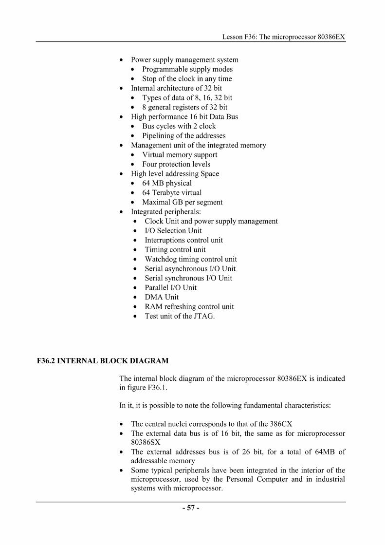
Lesson F36: The microprocessor 80386EX
- 57 -
• Power supply management system• Programmable supply modes• Stop of the clock in any time
• Internal architecture of 32 bit• Types of data of 8, 16, 32 bit• 8 general registers of 32 bit
• High performance 16 bit Data Bus• Bus cycles with 2 clock• Pipelining of the addresses
• Management unit of the integrated memory• Virtual memory support• Four protection levels
• High level addressing Space• 64 MB physical• 64 Terabyte virtual• Maximal GB per segment
• Integrated peripherals:• Clock Unit and power supply management• I/O Selection Unit• Interruptions control unit• Timing control unit• Watchdog timing control unit• Serial asynchronous I/O Unit• Serial synchronous I/O Unit• Parallel I/O Unit• DMA Unit• RAM refreshing control unit• Test unit of the JTAG.
F36.2 INTERNAL BLOCK DIAGRAM
The internal block diagram of the microprocessor 80386EX is indicatedin figure F36.1. In it, it is possible to note the following fundamental characteristics: • The central nuclei corresponds to that of the 386CX• The external data bus is of 16 bit, the same as for microprocessor
80386SX• The external addresses bus is of 26 bit, for a total of 64MB of
addressable memory• Some typical peripherals have been integrated in the interior of the
microprocessor, used by the Personal Computer and in industrialsystems with microprocessor.

Lesson F36: The microprocessor 80386EX
- 58 -
The detailed description of the integrated peripherals is shown in thenext paragraph.
fig. F36.1
Lesson F36: The microprocessor 80386EX
- 59 -
F36.3 The INTEGRATED PERIPHERALS
The integrated peripherals at the interior of microprocessor 80386EX.are illustrated next. As seen before, they are peripherals normally used in the personalcomputer or in systems with industrial type microprocessors. ICU InterruptControl Unit
Consists of two controllers with programmableinterruptions 82C59A configured as master/slave.
TCU Timer ControlUnit
Provides 3 independent backward counters of 16 bit. Itis functionally equivalent to 3 timer counters, 82C54.
SIO AsynchronousSerial I/O
Contains 2 asynchronous units UART, functionallyequivalent to NS16450. Each channel contains a baud-rate generator, receiver, transmitter and modem controlunit.
DMA Direct MemoryAccessController
Transfers internal or external data between anycombination of memory or I/O devices throughout theentire addressing space of 26 bit. It is compatible with the controllers 8237A.
SMM SystemManagementMode
Provides a mechanism for the management of thesystem with a hardware and software combination.Drives an external line SMI# which can generatetransparent interruptions to the operative system.
Clock andPowerManagementUnit
An external source has to provide the clock to themicroprocessor, which then sends it to the base nucleiand to the internal peripherals. The management unit of the power supply gives thepossibility to stop the microprocessor in order to limitthe current consumption.
SSIO SynchronousSerial I/O Unit
Provides a high-speed synchronous bi-directional I/Ochannel. Consists of a transmission channel, one forreception and a baud-rate generator.
CSU Chip SelectUnit
This programmable unit of 8 channels provides thedirect access to 8 external units. Each channel canoperate at 8 o 16 bit and can generate up to 31 waitstates.
RCU RefreshControl Unit
Offers the possibility of generating periodicalrefreshing requests and corresponding addresses. It isused in systems with dynamic RAM.
Parallel I/OPorts
Provides 3 programmable I/O ports. The pins at theoutputs of these I/O ports are in multiplexer with otherfunctions.

Lesson F36: The microprocessor 80386EX
- 60 -
WDT WatchdogTimer Unit
When enabled, this unit operates as a timer of genericuse at 32 bit.
JTAG Test-logic Unit
This unit simplifies the testing of the cards. Resultscompatible with the standard IEEE.

Lesson F36: The microprocessor 80386EX
- 61 -
F36.3 The BUS INTERFACE UNIT
The microprocessor communicates with the memory, the I/O, and withother devices by means of operations on the bus. Addresses, data, state, and control information define a bus cycle. The Bus Interface Unit (BIU) supports cycles of reading and writingwith external memory and I/O devices; it contains additionally, signals,which allow an external microprocessor to take control of the bus. The signals driven by the BIU are the following (see also the data sheetof the microprocessor in the appendix):
Signal Description A25:1 Bus of the addresses: selects memory devices or
external I/O. These signals are valid when ADS# is active andremain active until the next T1, T2P or Ti.
ADS# Address Strobe: indicates that the processor isgenerating a valid bus cycle. The processor drivesW/R#, D/C#, M/IO#, WR#, RD#, UCS#, CS6:0#,LOCK#, REFRESH#, A25:1, BHE# and BLE#.
BHE# BLE#
Byte enabling output: indicates which byte of the 16 bitof the data bus is being transferred. BHE# BLE# Output 0 0 Word Transfer 0 1 Superior byte Transfer (D15:8) 1 0 Inferior byte Transfer (D7:0) 1 1 Refreshing Cycle
BS8# Amplitude of the bus: indicates that the deviceaddressed at the time is of 8 bit
D15:0 Data Bus: for the reading and writing operations of thememory and of the I/O
LBA Local Bus Access: indicates that the microprocessor isfurnishing the signal READY# internally to end atransaction on the bus.
LOCK Bus Lock: Hinders other microprocessors on the bus oftaking control of the bus self.
M/IO# D/C# W/R# REFRESH#
Signals for cycle definition on the bus. Define thecurrent type of cycle. See the following table.
NA# Next address: used in the pipelining. RD# Read enable: indicates a reading cycle on the bus. READY# Serves to terminate the cycle on the bus WR# Write enable: indicates a writing cycle on the bus.
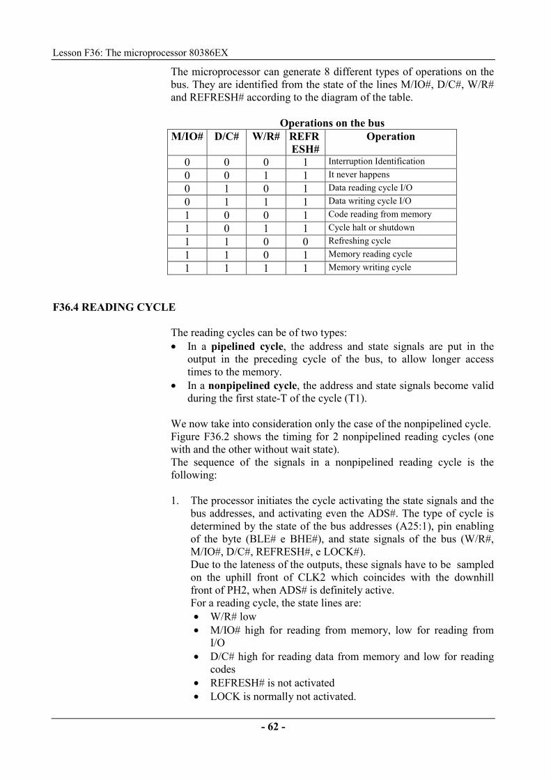
Lesson F36: The microprocessor 80386EX
- 62 -
The microprocessor can generate 8 different types of operations on thebus. They are identified from the state of the lines M/IO#, D/C#, W/R#and REFRESH# according to the diagram of the table.
Operations on the bus M/IO# D/C# W/R# REFR
ESH# Operation
0 0 0 1 Interruption Identification 0 0 1 1 It never happens 0 1 0 1 Data reading cycle I/O 0 1 1 1 Data writing cycle I/O 1 0 0 1 Code reading from memory 1 0 1 1 Cycle halt or shutdown 1 1 0 0 Refreshing cycle 1 1 0 1 Memory reading cycle 1 1 1 1 Memory writing cycle
F36.4 READING CYCLE The reading cycles can be of two types:• In a pipelined cycle, the address and state signals are put in the
output in the preceding cycle of the bus, to allow longer accesstimes to the memory.
• In a nonpipelined cycle, the address and state signals become validduring the first state-T of the cycle (T1).
We now take into consideration only the case of the nonpipelined cycle. Figure F36.2 shows the timing for 2 nonpipelined reading cycles (onewith and the other without wait state). The sequence of the signals in a nonpipelined reading cycle is thefollowing: 1. The processor initiates the cycle activating the state signals and the
bus addresses, and activating even the ADS#. The type of cycle isdetermined by the state of the bus addresses (A25:1), pin enablingof the byte (BLE# e BHE#), and state signals of the bus (W/R#,M/IO#, D/C#, REFRESH#, e LOCK#). Due to the lateness of the outputs, these signals have to be sampledon the uphill front of CLK2 which coincides with the downhillfront of PH2, when ADS# is definitely active. For a reading cycle, the state lines are:• W/R# low• M/IO# high for reading from memory, low for reading from
I/O• D/C# high for reading data from memory and low for reading
codes• REFRESH# is not activated• LOCK is normally not activated.
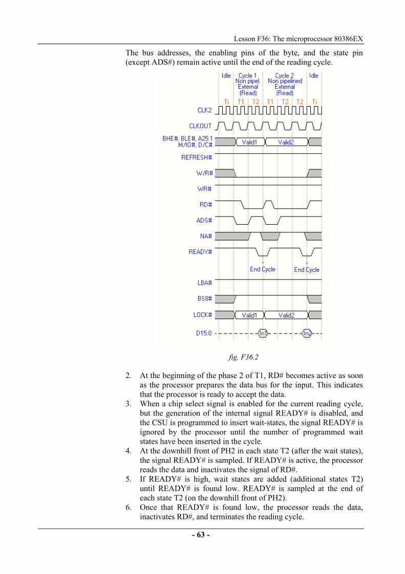
Lesson F36: The microprocessor 80386EX
- 63 -
The bus addresses, the enabling pins of the byte, and the state pin(except ADS#) remain active until the end of the reading cycle.
fig. F36.2
2. At the beginning of the phase 2 of T1, RD# becomes active as soon
as the processor prepares the data bus for the input. This indicatesthat the processor is ready to accept the data.
3. When a chip select signal is enabled for the current reading cycle,but the generation of the internal signal READY# is disabled, andthe CSU is programmed to insert wait-states, the signal READY# isignored by the processor until the number of programmed waitstates have been inserted in the cycle.
4. At the downhill front of PH2 in each state T2 (after the wait states),the signal READY# is sampled. If READY# is active, the processorreads the data and inactivates the signal of RD#.
5. If READY# is high, wait states are added (additional states T2)until READY# is found low. READY# is sampled at the end ofeach state T2 (on the downhill front of PH2).
6. Once that READY# is found low, the processor reads the data,inactivates RD#, and terminates the reading cycle.

Lesson F36: The microprocessor 80386EX
- 64 -
F36.4 WRITING CYCLE The reading cycles can be of two types:• pipelined cycle• nonpipelined cycle We now take into consideration only the case of the nonpipelined cycle. Figure F36.3 shows the timing for 2 nonpipelined writing cycles (onewith and the other without wait state). The sequence of the signals in a nonpipelined writing cycle is thefollowing: 1. The processor initiates the cycle activating the state signals and the
bus addresses, and activating even the ADS#. The type of cycle isdetermined by the state of the bus addresses (A25:1), pin enablingof the byte (BLE# e BHE#), and state signals of the bus (W/R#,M/IO#, D/C#, REFRESH#, e LOCK#). Due to the lateness of the outputs, these signals have to be sampledon the uphill front of CLK2 which coincides with the downhillfront of PH2, when ADS# is definitely active. For a reading cycle, the state lines are:• W/R# low• M/IO# high for reading from memory, low for reading from
I/O• D/C# high for reading data from memory and low for reading
codes• REFRESH# is not activated• LOCK is normally not activated.
The bus addresses, the enabling pins of the byte, and the state pin(except ADS# and WR#) remain active until the end of the readingcycle. 2. At the beginning of the phase 2 of T1, WR# becomes active and the
processor initiates piloting the data bus. The data remains validuntil the beginning of the phase 2 in the state-T after the present buscycle is terminated.
3. When a chip select signal is enabled for the current reading cycle,but the generation of the internal signal READY# is disabled, andthe CSU is programmed to insert wait-states, the signal READY# isignored by the processor until the number of programmed waitstates have been inserted in the cycle.
4. The signal WR# can be disabled in 2 modes:Early Ready: WR# is disabled on the uphill front of CLK2 in themiddle of state T2, after the wait states are finished.On the uphill front of PH2, READY# is sampled. If it is foundactive, WR# is disabled in a synchronous mode in the middle ofT2, guided from the uphill front of clock PH2. The writing cycleis then terminated at the end of the state T2.

Lesson F36: The microprocessor 80386EX
- 65 -
Late Ready: When READY# goes low after the uphill front ofPH2 of the state T2 (after the programmed wait states), WR# isdisabled in a synchronous mode as soon READY# is activated(after a small lateness caused by the logic circuits). The writingcycle is then terminated at the end of the state T2.
The signal WR# operates in this mode to ensure a time ofsufficient duration for the addresses and for the enabling signal othe external device.
5. If READY# is high, wait states are added (additional states T2)until READY# is found low. READY# is sampled in each state T2(on the uphill front of PH2) to disable the signal WR# in anappropriate mode.
6. Once the READY# is found low, the writing cycle is terminated.
fig. F36.3
Lesson F36: The microprocessor 80386EX
- 66 -
F36.5 SUMMARY QUESTIONNAIRE
���� Z3
���� SIS1
���� SIS2 Insert code Lesson: F36
Q1 Which of the following xspressions, referring the microprocessor80386EX is not true ? SETA B 1 5 The addresses bus is of 32 bit 2 4 The data bus is of 16 bit 3 2 The internal registers are of 32 bit 4 3 Addresses up to 64 MB of memory 5 1 Can be used in multi-user systems
Q2 What is the function of the integrated peripheral SIO ? SETA B 1 4 Provides N.2 serial asynchronous interface 2 3 Provides one serial synchronous interface 3 1 Provides the I/O ports 4 5 Provides the enabling of I/O devices 5 2 Provides a programmable timer
Q3 Which of the following signals of the microprocessor 80386EX indicatewho is transferring the most significant byte in an external operation at16 bit ? SETA B 1 4 BLE# 2 5 BHE# 3 1 BS8#4 2 ADS#5 3 D/C#
Lesson F36: The microprocessor 80386EX
- 67 -
Q4 Which of the following signals of the microprocessor 80386EX indicate
that a valid bus cycle is being followed? SETA B 1 4 BLE# 2 5 M/IO# 3 4 BS8# 4 1 ADS# 5 2 M/IO#
Q5 In a reading cycle the signal of READY# determines ? SETA B 1 3 that the cycle is initiated 2 1 that the microprocessor is ready to read the data 3 2 that the peripheral is ready to provide the data

Lesson F37: The 32 bit Microprocessor Trainer Mod. Z3/EV
- 68 -
LESSON F37: THE 32-BIT MICROPROCESSOR TRAINER mod. Z3/EV
OBJECTIVES• General description of Module Z3/EV• The composing units• The Monitor commands
MATERIALS
• Base unit for the IPES system (power supply mod.PS1-PSU/EV,module holder mod.MU/EV, individual management unitmod.SIS1/SIS2/SIS3)
• Experimentation module mod. Z3/EV• oscilloscope. In this lesson, the 32 Bit Microprocessor Trainer Mod. Z3/Ev isillustrated . It’s important since starting the next lesson, programs to be used withthis system will be proposed.
F37.1 GENERAL DESCRIPTION
The 32 Bit Microprocessor Trainer (Module Z3/EV) is a didacticalsystem with microprocessor, based on the 80386 Intel, which allowsfacing all the problematic related to the study and use of microprocessorsystems.It possesses all the typical components necessary for the study of thistype of systems: microprocessor, memories RAM and EPROM,keyboard and liquid crystal display, serial and parallel interface, analoginputs and outputs. It contains also the connector for fault insertion ofthe System IPES, which allows facing the problematic of fault researchin systems with microprocessors.The main characteristics of the system are:• microprocessor 386EX at 2.21 MHz• 32 KB EPROM system, 32 KB EPROM user, 32 KB RAM static• hexadecimal/commands keyboard, display LCD with a line of 16
characters• parallel interface (8+8+4 I/O lines), serial interface RS-232• analog inputs and outputs 0-8V converter at 8 bit• logic probes• single voltage supply 5V• Monitor in EPROM with commands for:
• visualization and modification of memory and registers• continuous execution, step by step, with programs breakpoints• charging of programs from PC.
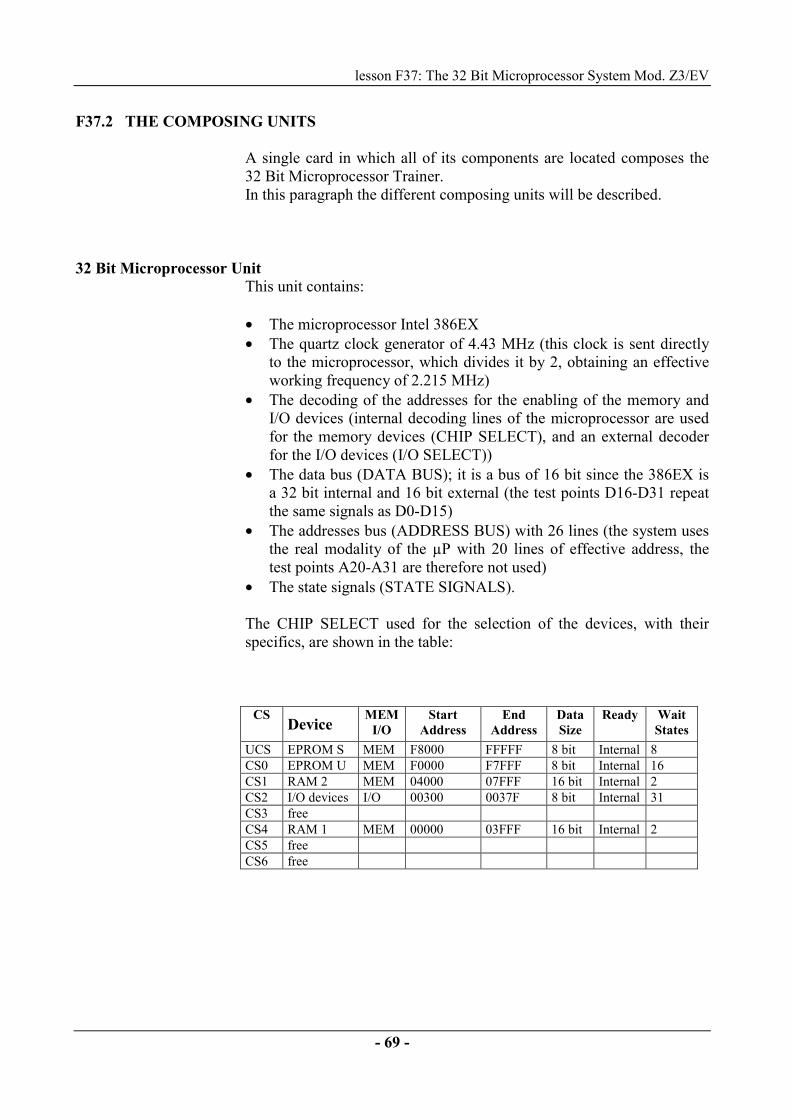
lesson F37: The 32 Bit Microprocessor System Mod. Z3/EV
- 69 -
F37.2 THE COMPOSING UNITS
A single card in which all of its components are located composes the32 Bit Microprocessor Trainer.In this paragraph the different composing units will be described.
32 Bit Microprocessor UnitThis unit contains:
• The microprocessor Intel 386EX• The quartz clock generator of 4.43 MHz (this clock is sent directly
to the microprocessor, which divides it by 2, obtaining an effectiveworking frequency of 2.215 MHz)
• The decoding of the addresses for the enabling of the memory andI/O devices (internal decoding lines of the microprocessor are usedfor the memory devices (CHIP SELECT), and an external decoderfor the I/O devices (I/O SELECT))
• The data bus (DATA BUS); it is a bus of 16 bit since the 386EX isa 32 bit internal and 16 bit external (the test points D16-D31 repeatthe same signals as D0-D15)
• The addresses bus (ADDRESS BUS) with 26 lines (the system usesthe real modality of the µP with 20 lines of effective address, thetest points A20-A31 are therefore not used)
• The state signals (STATE SIGNALS).
The CHIP SELECT used for the selection of the devices, with theirspecifics, are shown in the table:
CS Device MEM
I/OStart
AddressEnd
AddressDataSize
Ready WaitStates
UCS EPROM S MEM F8000 FFFFF 8 bit Internal 8CS0 EPROM U MEM F0000 F7FFF 8 bit Internal 16CS1 RAM 2 MEM 04000 07FFF 16 bit Internal 2CS2 I/O devices I/O 00300 0037F 8 bit Internal 31CS3 freeCS4 RAM 1 MEM 00000 03FFF 16 bit Internal 2CS5 freeCS6 free
Lesson F37: The 32 bit Microprocessor Trainer Mod. Z3/EV
- 70 -
The I/O SELECT used for the selection of the I/O devices, with theirspecifics, are shown in the table:
Addresses Devices300 – 30F Converter D/A310 – 31F Parallel Interface320 – 32F Keyboard330 – 33F Serial Interface340 – 34F A/D Converter350 – 35F Liquid Crystal Display360 – 36F Free370 – 37F Free
Memory UnitThe memory unit contains the following devices, with thecorresponding addresses at the interior of the system:
Memory Devices AddressInitial
AddressFinale
EPROM system 32K IC5 F8000 FFFFFEPROM user 32K IC6 F0000 F7FFFRAM 32K IC7-8-9-10 00000 07FFF
The EPROM memories are set in such a way to operate with themicroprocessor 80386EX with data transfer at 8 bit.The RAM memories are set in a way to operate at 16 bit, therefore,there are always used N.2 memories in couple for the least significantbyte (IC7, IC9) and N.2 memories for the most significant byte (IC8,IC10).
At the time of power on, the EPROM memory of the system is enabledand the microprocessor follows the instruction at address FFFF0, wherethe Monitor program begins.
The EPROM of the system is reserved for the memorization ofprograms developed by the user, which have to be set available in thesystem.
With respect to the RAM, it contains:
� the area reserved to the interruption vectors� the area reserved to the system� the user area.
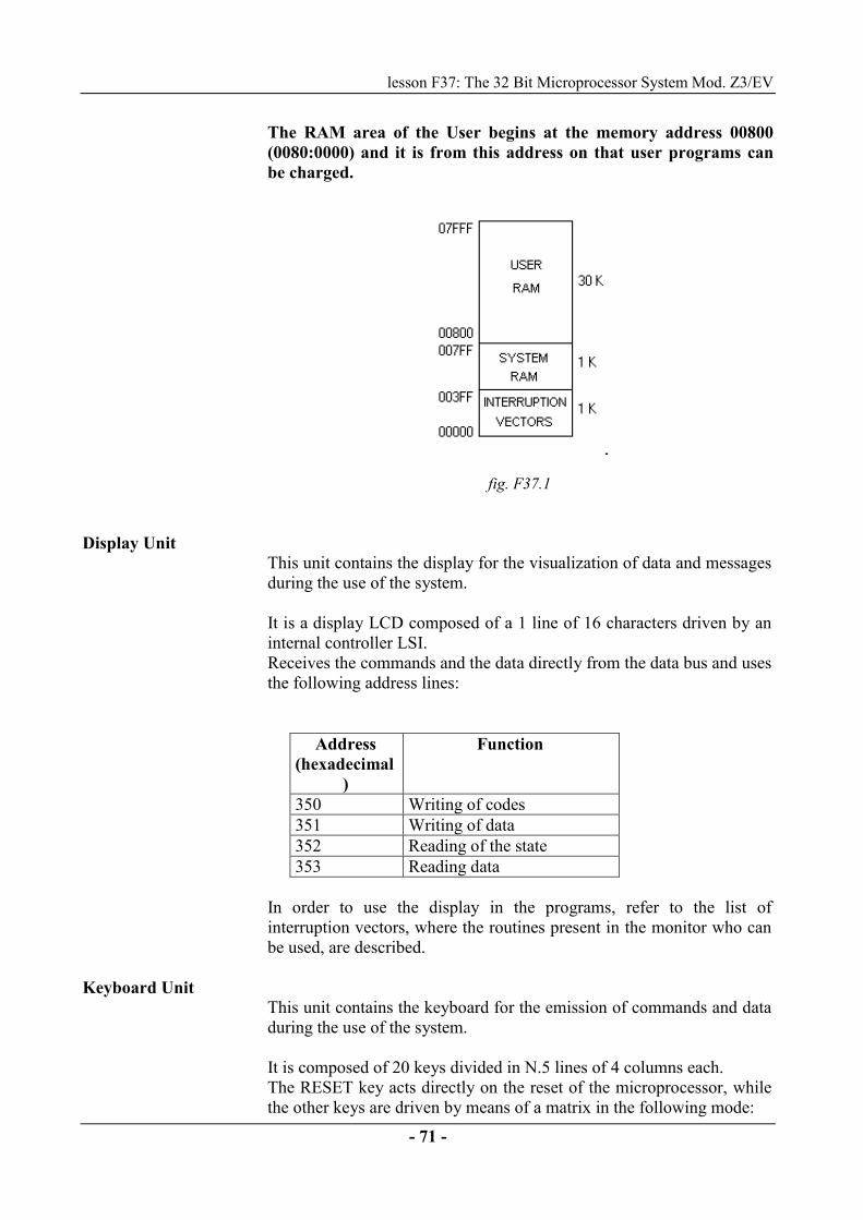
lesson F37: The 32 Bit Microprocessor System Mod. Z3/EV
- 71 -
The RAM area of the User begins at the memory address 00800(0080:0000) and it is from this address on that user programs canbe charged.
fig. F37.1
Display Unit This unit contains the display for the visualization of data and messagesduring the use of the system. It is a display LCD composed of a 1 line of 16 characters driven by aninternal controller LSI. Receives the commands and the data directly from the data bus and usesthe following address lines:
Address(hexadecimal
)
Function
350 Writing of codes 351 Writing of data 352 Reading of the state 353 Reading data
In order to use the display in the programs, refer to the list ofinterruption vectors, where the routines present in the monitor who canbe used, are described.
Keyboard Unit This unit contains the keyboard for the emission of commands and dataduring the use of the system. It is composed of 20 keys divided in N.5 lines of 4 columns each. The RESET key acts directly on the reset of the microprocessor, whilethe other keys are driven by means of a matrix in the following mode:

Lesson F37: The 32 bit Microprocessor Trainer Mod. Z3/EV
- 72 -
COL1
(32E) COL2 (32D)
COL3 (32B)
COL4 (327)
Riga 1(D0)
Key N.17
Key N.18
Key N.19
Key Reset
Riga 2 (D1)
Key N.13
Key N.14
Key N.15
Key N.16
Riga 3 (D2)
Key N.9
Key N.10
Key N.11
Key N.12
Riga 4 (D3)
Key N.5
Key N.6
Key N.7
Key N.8
Riga 5 (D4)
Key N.1
Key N.2
Key N.3
Key N.4
The columns correspond to different I/O addresses (32E, 32D, 32B,327), while the lines correspond to different bit of the data bus (D0, D1,D2, D3, D4). In order to use the keyboard in the programs, refer to the list ofinterruption vectors, where the routines present in the monitor who canbe used, are described.
Parallel I/O Unit This unit contains a controller of parallel interface of the type 8255,which makes available N.3 I/O parallel ports. The module Z3 uses N.2 ports of 8 bit (Port A and Port B) and N.4 I/Olines coming from Port C (PC0-PC3). A line of the Port C (PC4) is then used to command the Buzzer. See the electrical diagram in the appendix of the manual to consult thepin-out of the output connector.
Serial I/O Unit This unit contains a controller of serial asynchronous interface of thetype 8250. It receives the clock at 1.8432 MHz from an external oscillator anddrives all the typical lines of an interface RS-232: TXD, RXD, CTS,RTS, DCD, DSR and DTR. The integrated circuits IC14 (1488) and IC15 (1489) manage to transferthe signals TTL (0-5V) coming out from the 8250 towards the level (-12V - +12V) foreseen by the standard RS-232. The output connector J2 has a pin-out equal to the analog connectors ofthe IBM compatibles PCs. See the electrical diagram in the appendix of the manual to consult thepin-out of the output connector.

lesson F37: The 32 Bit Microprocessor System Mod. Z3/EV
- 73 -
Analog I/O Unit This unit contains an A/D converter and an D/A converter of 8 bit. Drives input and output analog signals in the range 0-8 Volt. The A/D conversion is done using the IC17 (ADC0804), which isconnected directly to the section at 8 bit (D0-D7) of themicroprocessor’s bus. The D/A conversion is done using the IC18 (74374) as latch for thedata coming from the bus D0-D7 of the microprocessor, and the IC19(DAC0800) for the D/A conversion.
Power Supply Unit This unit contains the supply section. It is set for the functioning with the single voltage supply of +5V. The voltages +12V e –12V, used by the Serial I/O Unit and by theAnalog I/O Unit, are taken internally at the module by means ofadequate converters DC-DC.
Logic Probes Unit This unit contains the logic probes, together with the correspondingvisualization LEDs of the state. In particular there are present:� N.8 logic probes TTL (0-5V), denominated D0-D7, with the
corresponding signaling LED D0-D7, which can be connected, bymeans of an adequate cable, to 8 test-points simultaneously.
� N.1 logic probe TTL, denominated DH, provided with pull-upresistance, with the corresponding signaling LED DH.
� N.1 logic probe TTL, denominated DL, provided with pull-downresistance, with the corresponding signaling LED DL.
� N.1 logic probe TTL, denominated DS, which acts on the transientsignals, with the corresponding signaling LED DH and with a resetkey RES-DS.
Faults Unit This unit contains the connector for the connection with the unit IPESMod. SIS1, SIS2 e SIS3 which manage the faults insertion. The faults can also be managed in local mode by means of dipswitchDP1 and DP2. In normal conditions, with no faults, DP2 has to be put all in ON,while DP1 has to be put all in OFF.

Lesson F37: The 32 bit Microprocessor Trainer Mod. Z3/EV
- 74 -
F37.3 The COMMANDS of the MONITOR
The MONITOR is the program, inserted in the interior of the EPROMof the system, which provides the management of the system and allowsthe user to work with it. Its fundamental functions are:
• visualization and modification of memory and registers• continuous execution, step by step, with programs breakpoints• charging of programs from keyboard and from PC.
The interaction with the user is done by means of keyboard and display. The meaning of the different keys on the keyboard is shown next. Fora detailed description of the Monitor commands refer to Appendix A.
KEY FUNCTION MEM Examines/changes the contents of the memory REG Examines/changes the contents of general registers SEG Examines/changes the contents of segment registers
LD_KB Charges a program from keyboard LD_PAR Charges a program by means of parallel interface LS_SER Charges a program by means of serial interface
RUN Follows a program from a fixed memory address GO Follows a program from any memory address SS Follows a program instruction and stops
GEN Free key BR Manages the breakpoints CB Cancels the displayed breakpoint INC Increments the memory address, the register or the
displayed breakpoint DEC Decrements the memory address, the register or the
displayed breakpoint FIRST Visualizes the first memory address, register or
breakpoint LAST Visualizes the last memory address, register or
breakpoint CHG/RET Switches into the modification mode (CHG) or
terminates the modification session (RET) and returnsto the command mode
���� Moves the cursor to the right during the datamodification
���� Moves the cursor to the left during the datamodification
RESET Provokes a reset of the microprocessor (this key isphysically connected to the reset of the micro).
lesson F37: The 32 Bit Microprocessor System Mod. Z3/EV
- 75 -
F37.4 SUMMARY QUESTIONNAIRE
���� Z3
���� SIS1 Set all the switches to the OFF position
���� SIS2 Insert code Lesson: F37
Q1 Which of the following combinations, represent in correct mode theamplitude of the data and addresses bus in Module Z3/EV ? SETA B 1 2 8, 16 2 4 16, 16 3 5 32, 32 4 1 16, 20 5 3 16, 32
Q2 How many bit does the microprocessor use when it reads or writes datain the RAM memory of Module Z3/EV? SETA B 1 5 8 bit 2 4 16 bit 3 2 20 bit 4 3 26 bit 5 1 32 bit
Q3 Which of the following units is not included in the 32 BitMicroprocessor Trainer Mod. Z3/EV ? SETA B 1 2 Serial asynchronous interface unit 2 4 Serial synchronous interface unit 3 1 Parallel interface unit4 5 Analog interface unit5 3 Display unit.
Lesson F37: The 32 bit Microprocessor Trainer Mod. Z3/EV
- 76 -
Q4 The Serial I/O Unit receives clock for the serial transmission of datafrom ? SETA B 1 4 An internal oscillator of the unit 2 3 Clock of the microprocessor 3 2 An internal oscillator of the controller 8250 4 1 Peripheral with which it communicates.
Q5 Which of the following functions is not implemented in the Monitor ofModule Z3/EV ? SETA B 1 6 Display/modification of general registers2 5 Display of the RAM memory3 4 Display of the EPROM memory 4 3 Display of the instructions of the microprocessor 5 2 Step by step of execution of a program 6 1 Insertion of breakpoints in the program.
Q6 In what memory address does the user RAM area begin, where theprograms can be charged? SETA B 1 3 0000:00002 5 0000:FFFF3 2 FFFF:FFF0 4 1 0000:0800 5 4 0000:07FF
lesson F37: The 32 Bit Microprocessor System Mod. Z3/EV
- 77 -
POWER ON, USE and TROUBLESHOOTING of the SYSTEM Switch on Module Z3/EV and verify that on the display the messagesystem ready to accept commands appears:
Command Prompt In the case in which this message does not appear, press the key Resetto initialize the microprocessor again. Try some of the commands of the monitor illustrated in the lesson.
���� SIS1 Set switch S2 in the ON position
���� SIS2 Press INS
Q7 The system is blocked and doesn’t respond to the introduced commands
from the keyboard anymore. What’s the reason for this malfunctioning? SETA B1 5 There is no supply of +5V to the microprocessor2 4 The reset signal of the microprocessor is active (+5V) 3 2 The clock signal has an amplitude too low 4 3 There is no clock signal of the microprocessor 5 1 The keyboard doesn’t work correctly.
���� SIS1 Set switch S2 in the OFF position
Set switch S16 in the ON position
���� SIS2 Press INS
Q8 The system is still blocked and continues to not respond to the
introduced commands from the keyboard. What’s the reason for thisnew malfunctioning ? SETA B1 4 There is no supply of +5V to the microprocessor2 3 The reset signal of the microprocessor is active (+5V) 3 2 The clock signal has an amplitude too low 4 1 The keyboard doesn’t work correctly.
���� SIS1 Set switch S16 in the OFF position
lesson F38: Advanced Programing
- 78 -
LESSON F38: ADVANCED PROGRAMMING
OBJECTIVES• The state flags• The instructions of unconditioned and conditioned jump• The subroutines• The stack and the instructions POP and PUSH• Development of application programs and exercises
MATERIALS
• Base unit for the IPES system (power supply mod.PS1-PSU/EV,module holder mod.MU/EV, individual management unitmod.SIS1/SIS2/SIS3)
• Experimentation module mod. Z3/EV• oscilloscope. This Lesson introduces some of the important characteristics ofprogramming with microprocessors and a guide to program constructionfor the System with 32 bit Microprocessor, using the assemblerlanguage.
F38.1 STATE FLAGS
We have already seen how the microprocessors 8086/80386 areprovided with a state register FLAGS/EFLAGS which indicates someconditions produced by the execution of the different operations. These conditions become very important in order to be able to make thedecisions during the execution of a program. The condition flags are 6: Flag carry (CF)
The carry flag is used to indicate that:� the result of the addition of two numbers of 8 bit produces a
number greater than 8 bit� the result of the addition of two numbers of 16 bit produces a
number greater than 16 bit� the result of the addition of two numbers of 32 bit produces a
number greater than 32 bit� the second number of a subtraction is greater than the first� the second operand in a comparison instruction (CMP) is
greater than the first
lesson F38: Advanced Programing
- 79 -
Parity Flag (PF)
The parity flag is used to indicate if in a binary word the numberof ‘1’ present is parity.
Auxiliary Carry Flag (AF) This flag is used in the BCD additions and subtractions. Acts insimilar mode to the carry flag, but considers only 4 bit.
Zero Flag (ZF) This flag is used to indicate if the result of an arithmetic or logicoperation is 0. It is set for the following typical situations:� subtraction of two equal numbers� comparison (CMP) of two equal numbers� decrement of a register which reaches the value 0� increment of a register, which currently contains its maximum
value.
Sign Flag (SF) When positive and negative numbers are to be manipulated, therepresentation in complement of 2 is used, where the mostsignificant bit (msb) gives the information corresponding to thesign:� msb = 1 for the negative numbers� msb = 0 for the positive numbers. The sign flag contains the information on the sign of the resultafter each arithmetic or logic operation.
Overflow Flag (OF) This flag indicates if the result of an operation with sign is too bigto be memorized in the number of bit available for it.
F38.2 INSTRUCTIONS of UNCONDITIONED and CONDITIONED JUMPING The jump instructions are used to tell a program to follow an instruction present in a data memory site, rather than that the next instruction in the sequence of the program.
Unconditioned jump (instruction JMP) The JMP instruction allows to pass to the execution of a new instructionpresent in any memory site. If this new site is present in the same code segment, the microprocessorchanges simply the contents of the register IP (Instruction Pointer) andthe jump is called near or intrasegment. If the new site is present in a different memory segment, then themicroprocessor has to change the contents of CS and of IP. In this case,the jump is called far o intersegment.
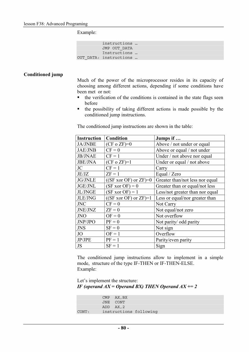
lesson F38: Advanced Programing
- 80 -
Example: instructions … JMP OUT_DATA Instructions … OUT_DATA: instructions …
Conditioned jump Much of the power of the microprocessor resides in its capacity ofchoosing among different actions, depending if some conditions havebeen met or not:� the verification of the conditions is contained in the state flags seen
before� the possibility of taking different actions is made possible by the
conditioned jump instructions. The conditioned jump instructions are shown in the table: Instruction Condition Jumps if …JA/JNBE (CF o ZF)=0 Above / not under or equalJAE/JNB CF = 0 Above or equal / not underJB/JNAE CF = 1 Under / not above nor equalJBE/JNA (CF o ZF)=1 Under or equal / not aboveJC CF = 1 CarryJE/JZ ZF = 1 Equal / ZeroJG/JNLE ((SF xor OF) or ZF)=0 Greater than/not less nor equalJGE/JNL (SF xor OF) = 0 Greater than or equal/not lessJL/JNGE (SF xor OF) = 1 Less/not greater than nor equalJLE/JNG ((SF xor OF) or ZF)=1 Less or equal/nor greater thanJNC CF = 0 Not CarryJNE/JNZ ZF = 0 Not equal/not zeroJNO OF = 0 Not overflowJNP/JPO PF = 0 Not parity/ odd parityJNS SF = 0 Not signJO OF = 1 OverflowJP/JPE PF = 1 Parity/even parityJS SF = 1 Sign
The conditioned jump instructions allow to implement in a simplemode, structure of the type IF-THEN or IF-THEN-ELSE. Example: Let’s implement the structure: IF (operand AX = Operand BX) THEN Operand AX += 2 CMP AX,BX JNE CONT ADD AX,2 CONT: instructions following

lesson F38: Advanced Programing
- 81 -
F38.3 PROCEDURE
When programs are written, there’s usually the necessity to use aparticular sequence of instructions in different points of a program. To avoid writing these instructions several times, they are written in aseparate part of the program called procedure. Each time that one wants to follow this sequence of instructions, theinstruction CALL is used, indicating the memory site where theprocedure begins. The instruction RET, at the end of the procedure, returns the control tothe following instruction to that which had called the procedure. To be able to obtain this, the instruction CALL saves automatically thereturn address in a particular memory area called stack. All of this is represented in figure F38.1.
fig. F38.1
Instruction CALL The instruction CALL follows two operations when it is called: � Memorizes the address of the successive instruction on the stack.
This is called return address. If the procedure called resides in thesegment itself, then the call is said to be near and is saved only IP,otherwise the call is said to be far and are saved CS and IP.
� Change the contents of IP with the address of the procedure if thecall is near, otherwise changes CS and IP if the call is far.
Instruction RET
The instruction RET behaves in a different mode depending if the callhas been near or far:� If the call is near, it simply picks a word from the stack and copies it
in IP provoking the execution of the instruction following the call.� If the call is far, it picks a word from the stack and copies it in IP
and successively picks another word and copies them in CS.
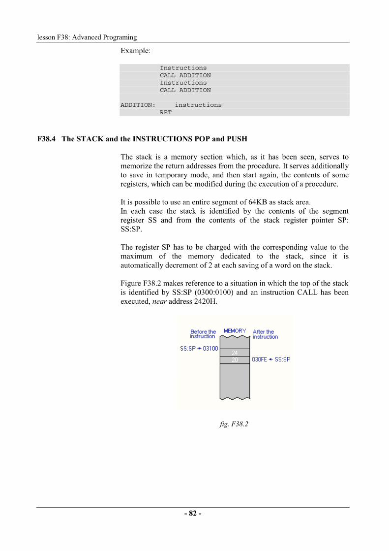
lesson F38: Advanced Programing
- 82 -
Example: Instructions CALL ADDITION Instructions CALL ADDITION ADDITION: instructions RET
F38.4 The STACK and the INSTRUCTIONS POP and PUSH
The stack is a memory section which, as it has been seen, serves tomemorize the return addresses from the procedure. It serves additionallyto save in temporary mode, and then start again, the contents of someregisters, which can be modified during the execution of a procedure. It is possible to use an entire segment of 64KB as stack area. In each case the stack is identified by the contents of the segmentregister SS and from the contents of the stack register pointer SP:SS:SP. The register SP has to be charged with the corresponding value to themaximum of the memory dedicated to the stack, since it isautomatically decrement of 2 at each saving of a word on the stack. Figure F38.2 makes reference to a situation in which the top of the stackis identified by SS:SP (0300:0100) and an instruction CALL has beenexecuted, near address 2420H.
fig. F38.2
lesson F38: Advanced Programing
- 83 -
In module Z3/EV there is a stack area of the system located in the lowerpart of the RAM memory. Normally, there is no need in the application programs to rechargeSS:SP with a different value, unless a lot of stack area is consumed. In this last case, we can charge SS:SP to the top of the RAM memorywith the following instructions: MOV AX,0700H ;value stack segment MOV SS,AX MOV AX,0FFFH ;value stack pointer MOV SP,AX
The instructions POP and PUSH Very often, at the interior of a procedure, general registers of themicroprocessor are used for the local elaboration. By doing this, theirvalues are modified and then, if the same registers were also used in themain program, we have a non-functioning of the program. In order to avoid this, the registers that are modified have to be saved onthe stack at the beginning of the procedure, and then restarted by takingthem from the stack at the end of the procedure. The instructions PUSH and POP allow to make this in a very simpleway. The instruction PUSH decrements the stack pointer in 2 and copies thecontents of the register in the stack. The instruction POP copies a word from the stack and puts it in theindicated register; the value of the stack pointer is then incremented by2. Example: PROC1 PROC NEAR PUSH AX ;saves AX on the stack MOV AX,0100H Other instructions POP AX ;resets AX RET PROC1 ENDP

lesson F38: Advanced Programing
- 84 -
F38.5 EXERCISES and SUMMARY QUESTIONNAIRE
���� Z3
���� SIS1 Set all switches in the OFF position
���� SIS2 Insert code Lesson: F38
Use of the instructions of conditioned jump
We would like to develop a program for the Module Z3/EV that simplywaits for a well-defined time, and then returns the control to theMonitor of the system. The list of the program is shown next. 1 PAGE 70,166 2 ;---------------- PRG_JUMP ------------------------- 3 ;this program follows a series of cycles 4 ;to determine a waiting time of several seconds 5 ;and then returns the control to the monitor 6 = 0007 IMONITOR EQU 07H 7 8 ;---------------------------------------- CODE 9 ;program charged in address 0000:MEM_POS 10 11 0000 PROG SEGMENT 12 ASSUME CS:PROG, DS:PROG 13 14 0000 B8 1000 START: MOV AX,1000 ;charges the counter AX 15 16 0003 B9 0108 LOOP2: MOV CX,108 ;charges the counter CX 17 0006 49 LOOP1: DEC CX ; 18 0007 83 F9 00 CMP CX,0000H ; 19 000A 75 FA JNZ LOOP1 ; 20 000C 48 DEC AX 21 000D 3D 0000 CMP AX,0000H 22 0010 75 F1 JNZ LOOP2 23 24 0012 CD 07 INT IMONITOR ;returns to the monitor 25 26 0014 PROG ENDS 27 END START
The instruction: INT MONITOR calls an software interruption which makes the microcontroller comeback under control of the monitor (this will be analyzed in the nextlesson). The waiting time is obtained with N.2 net cycles. The most internal cycle charges the register CX with the number 108and then decrements it down to zero. The external cycle uses as a counter, register AX. This cycle repeatsitself for 10000 times. Insert this program in Module Z3/EV using the keyboard.
lesson F38: Advanced Programing
- 85 -
Give the command: LD_KB Specify the departing address: 0000:0800 Insert the program codes: B8, 10, 27, B9, 6C, 00, ……, 07 Follow the program with the command RUN.
Q1 How much time goes by from the beginning of the program until thereturn to the monitor ? SETA B 1 4 1.5 seconds 2 5 5 seconds 3 1 10 seconds 4 2 15 seconds 5 3 20 seconds

lesson F38: Advanced Programing
- 86 -
Use of the procedure
We would like to develop a program for the Module Z3/EV that emits 3beeps from the buzzer, at fixes time intervals, and then return thecontrol to the Monitor of the system. A procedure is used to obtain the time intervals . This procedure is thencalled 2 times. The list of the program is shown next. 1 PAGE 70,166 2 ;-------------------------- PRG_CALL --------------- 3 ;this emits 3 beeps from the buzzer, at 4 ;fixed time intervals. 5 ;A procedure is used, called 2 times, 6 ;to obtain the time intervals. 7 = 0007 IMONITOR EQU 07H 8 = 0010 IBUZZER EQU 10H 9 = 0012 IPARAL EQU 12H 10 11 ;---------------------------------------- CODE 12 ;program charged in address 0000:0800H 13 14 0000 PROG SEGMENT 15 ASSUME CS:PROG, DS:PROG 16 17 0000 B4 00 START: MOV AH,00H 18 0002 B0 00 MOV AL,00H 19 0004 CD 12 MOV IPARAL ;out port 20 0006 BB 00C8 MOV BX,200 ;duration beep 21 0009 B9 0014 MOV CX,20 ;frequency beep 22 000C CD 10 INT IBUZZER ;--------------- BEEP1 23 000E E8 0026 R CALL ATT ;wait 24 0011 BB 00C8 MOV BX,200 ; 25 0014 B9 0014 MOV CX,20 ; 26 0017 CD 10 INT IBUZZER ;--------------- BEEP2 27 0019 E8 0026 R CALL ATT ;wait 28 001C BB 00C8 MOV BX,200 ; 29 001F B9 0014 MOV CX,20 ; 30 0022 CD 10 INT IBUZZER ;--------------- BEEP3 31 32 0024 CD 07 INT IMONITOR ;return to the monitor 33 34 ;procedure of waiting 35 0026 ATT PROC NEAR 36 0026 50 PUSH AX ;saves the used registers 37 0027 51 PUSH CX 38 0028 B8 03E8 MOV AX,1000 ;charges the counter AX 39 002B B9 0064 LOOP2: MOV CX,100 ;charges the counter CX 40 002E 49 LOOP1: DEC CX ;loop 41 002F 83 F9 00 CMP CX,0000H ; 42 0032 75 FA JNZ LOOP1 ; 43 0034 48 DEC AX 44 0035 3D 0000 CMP AX,0000H 45 0038 75 F1 JNZ LOOP2 46 003A 59 POP CX ;resets registers 47 003B 58 POP AX 48 003C C3 RET 49 003D ATT ENDP 50 003D PROG ENDS 51 END START
The interruption software is used: INT IBUZZER to command the buzzer. Before using it, charge the register BX with a value that determines theduration of the emitted signal and the register CX with the frequency. Insert this program in Module Z3/EV using the keyboard. Give the command: LD_KB

lesson F38: Advanced Programing
- 87 -
Specify the departing address: 0000:0800 Insert the codes of the program, reading them from the list. Follow the program with the command RUN.
Q2 How much time goes by from the beginning of the program until thereturn to the monitor ? SETA B 1 5 0.5 seconds 2 4 1 second 3 2 3 seconds 4 3 5 seconds 5 1 10 seconds
Q3 What is the contents of the register CX at the end of the programexecution? SETA B 1 4 0000:0000 2 1 FFFF 3 5 0000 4 3 0000FFFF 5 2 any
Q4 What is the contents of the register BX at the end of the programexecution? SETA B 1 2 0000:0000 2 4 FFFF 3 1 0000 4 5 0000FFFF 5 3 any
Lesson F39: Management of the Interruptions
- 88 -
LESSON F39: MANAGEMENT OF THE INTERRUPTIONS
OBJECTIVES• The sources of interruption• Interruptions and response to the interruptions• Types of interruptions• Interruptions software• Interruptions hardware• Priority of the interruptions• The interruptions software of Module Z3/EV• Development of application programs and exercises.
MATERIALS
• Base unit for the IPES system (power supply mod.PS1-PSU/EV,module holder mod.MU/EV, individual management unitmod.SIS1/SIS2/SIS3)
• Experimentation module mod. Z3/EV• oscilloscope.
F39.1 The SOURCES OF INTERRUPTION
The major part of the microprocessors allow the interruption by anexternal signal or by instructions of the program self, of the normalexecution of a program. In response to these interruptions, the microprocessor stops theexecution of the running program and calls a service procedure of theinterruption. A special instruction at the end of the service procedure of theinterruption, returns the execution of the program that was interrupted . For the microprocessor 80386EX an interruption can take place in threedifferent ways: � Interruption hardware: with the application of a signal on the
external line of NMI (Non Maskable Interrupt) or on the interruptionlines INT0, INT1, .. .
� Interruption software: with the execution of an instruction INT.
� When special error conditions take place, which happen during theexecution of an instruction (Ex. overflow, division by zero).

Lezione F39: Management of the Interruptions
- 89 -
F39.2 INTERRUPTIONS and RESPONSE to the INTERRUPTIONS
When an interruption is required, the microprocessor follows insequence the following actions to respond to the interruption: � Decrements the stack pointer in 2 and sets the flags register on the
stack� Disables other eventual interruptions setting to zero the interruption
flag IF in the flag register.� Resets the flag ‘trap’ (TF) in the flag register.� Decrements the stack pointer in 2 and puts in the stack the current
value of the segment register CS.� Decrements the stack pointer again in 2 and puts in the stack the
current value of the pointer register (IP).� Follows a jump of type far at the beginning of the procedure, which
has to respond to the instruction. The departing addresses of the procedure which have to respond to theinterruptions are memorized in a table which resides in the first KB ofthe RAM memory of the system, in the addresses from 00000H to003FFH. The departing addresses are called interruption vectors and the table iscalled interruption vectors table. The interruption vectors table contains 256 vectors and each one ofthem occupies 4 bytes (2 for the CS and two for the IP). Figure F39.1 shows the interruption vectors table. Note how for each vector the 2 least significant bytes contain the IP andthe MSB contain the CS.
fig. F39.1 At the end of a service procedure of the interruptions, the instructionIRET has to be used to return to the program which had beeninterrupted, in a correct way. The instruction IRET picks from the stack, in the following order� the IP value, and increments the stack by 2,� the CS value, and increments the stack by 2� the flags register value, and increments the stack by 2.
Lesson F39: Management of the Interruptions
- 90 -
F39.3 TYPES of INTERRUPTIONS
It has been seen how the management of the interruptions is done bymeans of the interruption vectors table. A number between 0 and 255characterizes each vector. This number is called the type of interruption. The types of smaller values are reserved to special interruptions, whilethe other are left free to the programmer. Next the types of reserved interruption will be described. Interruption type 0 – Division by zero.
This interruption is required automatically if, after the executionof a division instruction, the quotient exceeds the maximum valueallowed by the instruction.
Interruption type 1 – Single-Step
This interruption is generated in the instruction following that inwhich the trap flag TF is set to 1 in the flags register. It is used tofollow a program and an instruction one at a time.
Interruption type 2 – Interruption non-mask
This interruption is generated by a signal transition from low tohigh on the external pin NMI of the microprocessor. This is theinterruption of maximum priority can never be disabled.
Interruption type 3 – Breakpoint
This is an interruption software and is generated by a specialinterruption request instruction, which occupies a single byte ofoperative code. It is used to insert breakpoints in a program duringthe debug phase.
Interruption type 4 - Overflow
This interruption is generated if the overflow flag OF becomesequal to 1 after the execution of an instruction and the instructionINTO has been inserted immediately after.
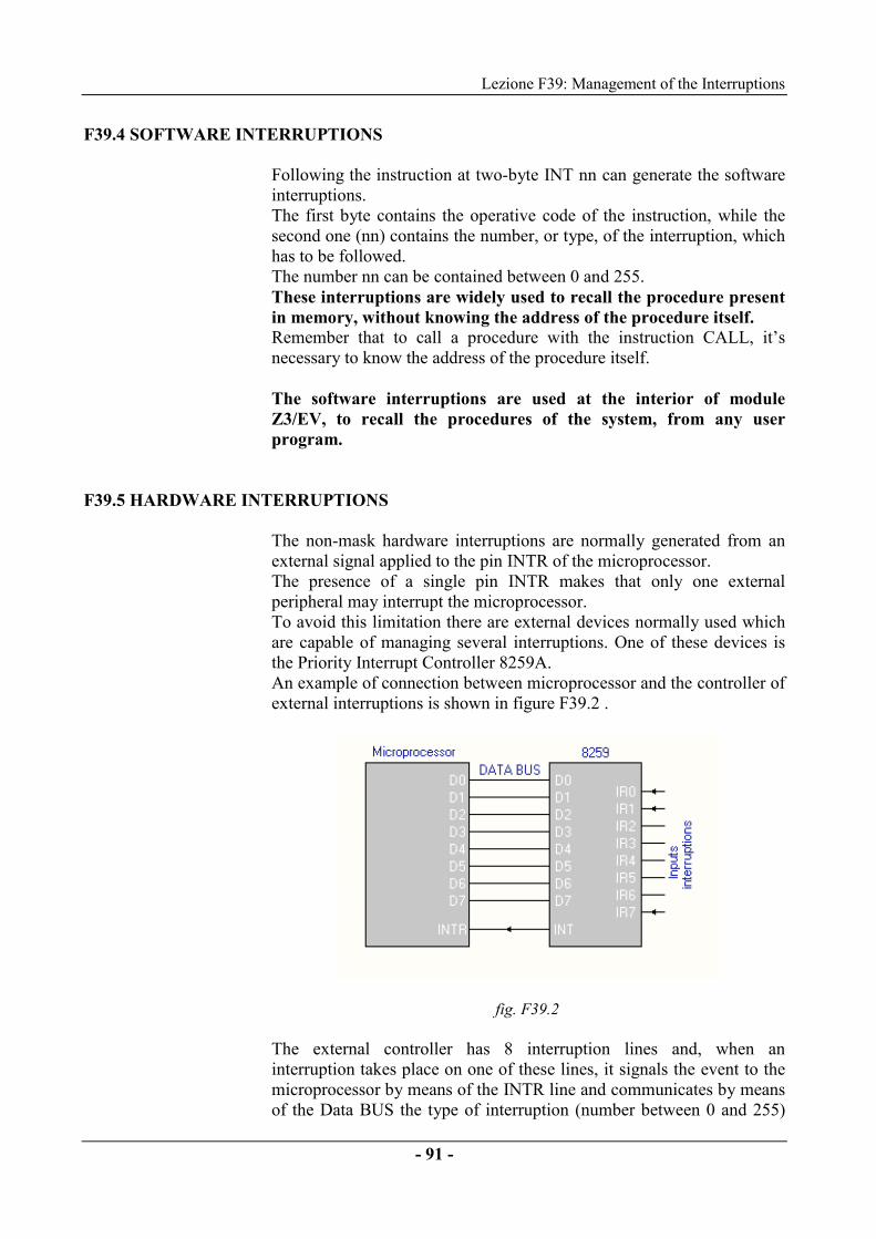
Lezione F39: Management of the Interruptions
- 91 -
F39.4 SOFTWARE INTERRUPTIONS
Following the instruction at two-byte INT nn can generate the softwareinterruptions. The first byte contains the operative code of the instruction, while thesecond one (nn) contains the number, or type, of the interruption, whichhas to be followed. The number nn can be contained between 0 and 255. These interruptions are widely used to recall the procedure presentin memory, without knowing the address of the procedure itself. Remember that to call a procedure with the instruction CALL, it’snecessary to know the address of the procedure itself. The software interruptions are used at the interior of moduleZ3/EV, to recall the procedures of the system, from any userprogram.
F39.5 HARDWARE INTERRUPTIONS
The non-mask hardware interruptions are normally generated from anexternal signal applied to the pin INTR of the microprocessor. The presence of a single pin INTR makes that only one externalperipheral may interrupt the microprocessor. To avoid this limitation there are external devices normally used whichare capable of managing several interruptions. One of these devices isthe Priority Interrupt Controller 8259A. An example of connection between microprocessor and the controller ofexternal interruptions is shown in figure F39.2 .
fig. F39.2 The external controller has 8 interruption lines and, when aninterruption takes place on one of these lines, it signals the event to themicroprocessor by means of the INTR line and communicates by meansof the Data BUS the type of interruption (number between 0 and 255)
Lesson F39: Management of the Interruptions
- 92 -
that has to be generated. These interruptions can be disabled by means of the instruction CLI(Clear Interrupt) and enabled by means of the instruction STI (SetInterrupt). The microprocessor 80386EX doesn’t have externally the line INTR,but has internally an Interruptions Control Unit formed by 2 controllers8259A put in cascade. For the details on the management of the interruptions within themicroprocessor 80286EX, refer to the manual of the microprocessor.
F39.6 PRIORITY of the INTERRUPTIONS
In the case in which more than one interruption takes placecontemporaneously, the microprocessor uses the technique of themaximum priority to serve the interruptions. The interruption with maximum priority is attended first; then the onewith a priority just below, and so on. The following table illustrates the priority of the interruptions:
Interruption Priority Error Division, INT nn, INTO
maximum
NMI INTR Single-Step minimum
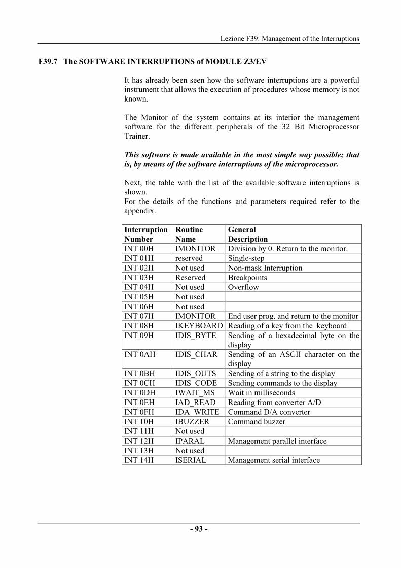
Lezione F39: Management of the Interruptions
- 93 -
F39.7 The SOFTWARE INTERRUPTIONS of MODULE Z3/EV
It has already been seen how the software interruptions are a powerfulinstrument that allows the execution of procedures whose memory is notknown. The Monitor of the system contains at its interior the managementsoftware for the different peripherals of the 32 Bit MicroprocessorTrainer.
This software is made available in the most simple way possible; thatis, by means of the software interruptions of the microprocessor.
Next, the table with the list of the available software interruptions isshown.For the details of the functions and parameters required refer to theappendix. InterruptionNumber
RoutineName
GeneralDescription
INT 00H IMONITOR Division by 0. Return to the monitor.INT 01H reserved Single-stepINT 02H Not used Non-mask InterruptionINT 03H Reserved BreakpointsINT 04H Not used OverflowINT 05H Not usedINT 06H Not usedINT 07H IMONITOR End user prog. and return to the monitorINT 08H IKEYBOARD Reading of a key from the keyboardINT 09H IDIS_BYTE Sending of a hexadecimal byte on the
displayINT 0AH IDIS_CHAR Sending of an ASCII character on the
displayINT 0BH IDIS_OUTS Sending of a string to the displayINT 0CH IDIS_CODE Sending commands to the displayINT 0DH IWAIT_MS Wait in millisecondsINT 0EH IAD_READ Reading from converter A/DINT 0FH IDA_WRITE Command D/A converterINT 10H IBUZZER Command buzzerINT 11H Not usedINT 12H IPARAL Management parallel interfaceINT 13H Not usedINT 14H ISERIAL Management serial interface

Lesson F39: Management of the Interruptions
- 94 -
F39.8 EXERCISES and SUMMARY QUESTIONNAIRE
���� Z3
���� SIS1 Set all switches in the OFF position
���� SIS2 Insert code Lesson: F39
Use of the software interruptions
We would like to develop a program for the Module Z3/EV that reads akey from the keyboard and visualizes the corresponding code on thedisplay. The list of the program is shown next. 1 PAGE 70,166 2 ;------------------ PRG_KB ------------------------ 3 ;reading of a key from the keyboard 4 ;and display of the code on the display 5 PAGE 70,166 6 = 0800 MEM_POS = 0800H 7 = 0080 DS_SEG = 0080H 8 = 0008 IKEYBOARD = 08H ;interruption reading keyboard 9 = 0009 IDIS_BYTE = 09H ;interruption visual. byte 10 = 000B IDIS_STR = 0BH ;interruption visual. string 11 12 ;---------------------------------------- CODE 13 ;program charged in address 0000:MEM_POS 14 0000 CODE SEGMENT 15 ASSUME CS:CODE, DS:CODE 16 0000 ORG 0H 17 0000 B8 0080 START: MOV AX,DS_SEG 18 0003 8E D8 MOV DS,AX ;charges data segment 19 0005 BE 0012 R MOV SI,OFFSET MSG 20 0008 CD 0B INT IDIS_STR ;display message MSG 21 000A CD 08 TLOOP: INT IKEYBOARD ;reads keyboard 22 000C B1 0D MOV CL,13 23 000E CD 09 INT IDIS_BYTE ;visualizes key code 24 0010 EB F8 JMP TLOOP 25 26 0012 4B 42 2C 20 68 65 MSG DB 'KB, hex key: xx ',00H 27 78 20 6B 65 79 3A 28 20 78 78 20 00 29 30 0023 CODE ENDS 31 END START
Insert this program in Module Z3/EV using the keyboard (in case inwhich a Personal Computer is used, use the application MODZ3 totransfer the program PRG_KB via serial or parallel, using the adequatecables issued). Give the command: LD_KB Specify the departing address: 0000:0800 Insert the codes of the program: B8, 80, 00, ……, 20, 00. Give the command GO 0080:0000 (or RUN) of program execution.
Lezione F39: Management of the Interruptions
- 95 -
Q1 What is the meaning of the instruction MOV SI, OFFSET MSG at line
18 of the program ? SETA B 1 5 Charges SI with the MSG string address referred to DS 2 4 Charges SI with the MSG string address referred to CS 3 2 Charges SI with the length of the string MSG 4 3 Charges SI with the first 2 bytes of the string MSG 5 1 Charges SI with the value of the string MSG
Q2 What is the meaning of the instruction MOV CL,13 at line 21 of theprogram ? SETA B 1 4 Charges CL with the position on the display 2 3 Charges CL with the byte to display 3 2 Charges CL with the bytes counter of the string MSG 4 1 Charges CL with the pointer on the display
���� SIS1 Set switch S8 in the ON position
���� SIS2 Press INS
Q3 By pressing the keys on the keyboard, the display visualizes now casualsymbols. What is the reason of this malfunctioning ? SETA B1 2 The display isn’t connected correctly to the bus of the
microprocessor (line D6 absent, continuously at level ‘0’)2 4 The display isn’t connected correctly to the bus of the
microprocessor (line D0 absent, continuously at level ‘1’)3 1 Misses the Enable signal on the display 4 5 Misses the R/W# signal on the display 5 3 The clock of the microprocessor is not in phase.

Lesson F39: Management of the Interruptions
- 96 -
���� SIS1 Set switch S8 in the OFF position
Set switch S14in the ON position
���� SIS2 Press INS
Q4 By pressing the keys on the keyboard, the display isn’t updatedanymore. What is the reason of this new malfunctioning? SETA B1 6 The Enable signal on the display is not correct2 5 The R/W# signal on the display is not correct 3 4 The RS signal on the display is not correct 4 3 The keys of the keyboard do not work 5 2 The signal at test point R1 of the keyboard is not correct 6 1 The signal at test point R5 of the keyboard is not correct.
���� SIS1 Set switch S14 in the OFF position
Lesson F40: EPROM Memories and Interfacing to µP
- 97 -
LESSON F40: EPROM MEMORY and INTERFACE to µP
OBJECTIVES• Types of non volatile memory• Base structure of the EPROM• EPROM 27C256 Characteristics• Interface with the 80386EX• Development of application programs and exercises.
MATERIALS
• Base unit for the IPES system (power supply mod.PS1-PSU/EV,module holder mod.MU/EV, individual management unitmod.SIS1/SIS2/SIS3)
• Experimentation module mod. Z3/EV• oscilloscope.
F40.1 TYPES of NON VOLATILE MEMORIES A system with microprocessor has need for a non volatile memory,which can maintain the information even when it is turned off, in orderto contain the base program necessary for its operation. This base program is called Monitor of the system. The main type of non-volatile memories are: ROM
(Read Only Memory). It is of a memory whose contents is writtendirectly during the fabrication process. Its use is convenient only forlarge numbers of fabrication.
PROM
(Programmable Read Only Memory). It is always of a non-volatilememory with only reading, whose contents can be written (only onetime) directly by the user.
EPROM
(Erasable Programmable Read Only Memory). It is of a non-volatilememory with only reading which the user, can write, but that canalso be cancelled by means of ultraviolet rays exposure. The writing and reading operations can be followed many times. Thistype of memory is the one most widely used in microprocessorsystems.

Lesson F40: EPROM Memories and Interfacing to µP
- 98 -
F40.2 BASE STRUCTURE of the EPROM
The EPROM memories are based on a MOS transistor structureorganized in matrix form, as shown in figure F40.1 . It normally contains ‘n’ words of 8 bit.
fig. F40.1 The selection of the different words by means of the address lines. Inthe figure there are N.2 address lines A0 and A1 present capable ofaddressing N.4 words. Each word corresponds to a line of 8 transistors. The Decoder sets a logic level 0 on the selected line, and the 8 outputs(D0, ..,D7) assume the low or high level depending if the correspondingtransistor MOS conducts or not. The conduction brings the transistor tosaturation, which short-circuits the signal Vdc towards ground. The MOS transistor normally have a very high impedance when theyare interdicted. This characteristic can be modified applying a highvoltage signal (normally between 20 and 30 Volt) at their gates. The programming of the device consists then in the sending of a highvoltage impulse to the gate of each MOS, which has to memorize alogic level 0. Exposing the transistors MOS to the ultraviolet light, the inverseprocess takes place and the transistor returns to the high impedancecondition resting the logic level 1. These memories can thus be easily written or cancelled.

Lesson F40: EPROM Memories and Interfacing to µP
- 99 -
F40.3 EPROM 27C256 CHARACTERISTICS
At the interior of Module Z3/EV, the memories EPROM 27C256 areused. They are memories, which can contain up to 256 Kbit of informationorganized in 32768 words of 8 byte ( 32 KB ). Requests only a single supply of +5V and are available in a standard 28-pin package. The main characteristics are indicated in the table: Internal configuration 32768 x 8 bit supply + 5 Volt Active mode consumption 25 mW (1 MHz) Stand-by consumption 5 µW Access time 100-150 ns Programming voltage +12.5 VDC Inputs and outputs TTL
The internal block diagram and the pin-out are shown in fig. F40.2 .
fig. F40.2

Lesson F40: EPROM Memories and Interfacing to µP
- 100 -
F40.4 INTERFACE with the 80386EX The connection diagram of the memories EPROM 27C256 with themicroprocessor 80386EX at the interior of module Z3/EV, is shown inFig. F40.3 . In figure F40.4 the timings for the reading operations of the EPROMmemory are shown.
fig. F40.3
fig. F40.4
Lesson F40: EPROM Memories and Interfacing to µP
- 101 -
From the preceding diagram we can notice that: � The reading operations from the memory EPROM are followed
using the bus of 8 bit.
� The selection line UCS# is used to enable the system EPROM. Theline UCS# is connected to the line BS8# which indicates themicroprocessor to use the 8 bit bus.
� The line UCS# becomes active, together with the address3FFFFF0H after the reset of the microprocessor. Keeping in mindthat the bus of 20 bit is being used, we can see how this addresscorresponds to the memory cell FFF0H of the EPROM. It is in thismemory cell where the first instruction of the program Monitor islocated.
� The line UCS# is then programmed in the Chip Select Unit tooperate in the range of addresses F8000H-FFFFFH, with bus of 8 bitand with the generation of the internal READY signal.
� The line CS0# is used to enable the memory EPROM N.2. This lineis programmed in the Chip Select Unit of the microprocessor tooperate in the range of addresses F0000H-F7FFFH, with bus of 8 bitand with the generation of the internal READY signal.
� The data are read from the 2 memories using the signal RD# of themicroprocessor to pilot the line OE# of the memory.
� The line A0 of the memory, not present in the addresses bus of themicroprocessor, is generated directly by means of the signal BLE#of the microprocessor itself (the signal which indicated that the lestsignificant byte of bus at 16 bit is being used).
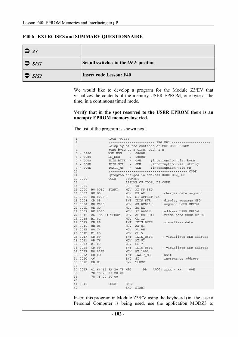
Lesson F40: EPROM Memories and Interfacing to µP
- 102 -
F40.6 EXERCISES and SUMMARY QUESTIONNAIRE
���� Z3
���� SIS1 Set all switches in the OFF position
���� SIS2 Insert code Lesson: F40
We would like to develop a program for the Module Z3/EV thatvisualizes the contents of the memory USER EPROM, one byte at thetime, in a continuous timed mode. Verify that in the spot reserved to the USER EPROM there is anunempty EPROM memory inserted. The list of the program is shown next. 1 PAGE 70,166 2 ;----------------------- PRG_EP2 -------------------- 3 ;display of the contents of the USER EPROM 4 ;one byte at a time, each 1 s 5 = 0800 MEM_POS = 0800H 6 = 0080 DS_SEG = 0080H 7 = 0009 IDIS_BYTE = 09H ;interruption vis. byte 8 = 000B IDIS_STR = 0BH ;interruption vis. string 9 = 000D IWAIT_MS = 0DH ;interruption wait ms 10 ;---------------------------------------- CODE 11 ;program charged in address 0000:MEM_POS 12 0000 CODE SEGMENT 13 ASSUME CS:CODE, DS:CODE 14 0000 ORG 0H 15 0000 B8 0080 START: MOV AX,DS_SEG 16 0003 8E D8 MOV DS,AX ;charges data segment 17 0005 BE 002F R MOV SI,OFFSET MSG 18 0008 CD 0B INT IDIS_STR ;display message MSG 19 000A B8 F000 MOV AX,0F000H ;segment USER EPROM 20 000D 8E C0 MOV ES,AX 21 000F BE 0000 MOV SI,0000H ;address USER EPROM 22 0012 26: 8A 04 TLOOP: MOV AL,ES:[SI] ;reads data USER EPROM 23 0015 B1 0C MOV CL,12 24 0017 CD 09 INT IDIS_BYTE ;visualizes data 25 0019 8B C6 MOV AX,SI 26 001B 8A C4 MOV AL,AH 27 001D B1 05 MOV CL,5 28 001F CD 09 INT IDIS_BYTE ; visualizes MSB address 29 0021 8B C6 MOV AX,SI 30 0023 B1 07 MOV CL,7 31 0025 CD 09 INT IDIS_BYTE ; visualizes LSB address 32 0027 B8 03E8 MOV AX,1000 33 002A CD 0D INT IWAIT_MS ;wait 34 002C 46 INC SI ;increments address 35 002D EB E3 JMP TLOOP 36 37 002F 41 64 64 3A 20 78 MSG DB 'Add: xxxx - xx ',00H 38 78 78 78 20 2D 20 39 78 78 20 20 00 40 41 0040 CODE ENDS 42 END START
Insert this program in Module Z3/EV using the keyboard (in the case aPersonal Computer is being used, use the application MODZ3 to

Lesson F40: EPROM Memories and Interfacing to µP
- 103 -
transfer the program PRG_EP2 via serial or parallel, using the adequatecables issued). Give the command: LD_KB Specify the departing address: 0000:0800 Insert the codes of the program as from the list. Give the command GO 0080:0000 (or RUN) for program execution.
Q1 What is the beginning physical address of the USER EPROM ? SETA B 1 2 0000:0000 2 5 00000 3 1 FFFFF4 3 0F0005 4 F0000
Q2 Which of the following activities is not carried out by themicroprocessor during the execution of the program ? SETA B 1 4 Reading from RAM M0L, M0H 2 1 Reading from SYSTEM EPROM 3 2 Reading from the keyboard 4 3 Writing on the display
���� SIS1 Set switch S7 in the ON position
���� SIS2 Press INS
Q3 The correct display of bytes of the EPROM memory has stopped. For
each cell the value FF is now displayed. What is the cause for thisfunctioning ? SETA B1 4 The data bus has been disconnected from the memory.2 1 The memory USER EPROM does not receive the enable3 5 The memory USER EPROM does not receive the reading command 4 2 The selection addresses of the USER EPROM cells are not
correct 5 3 The clock of the microprocessor has stopped.
Lesson F40: EPROM Memories and Interfacing to µP
- 104 -
���� SIS1 Set switch S7 in the OFF position
Q4 The memory USER EPROM is connected to the microprocessor bymeans of a bus of 8 bit. How is the microprocessor advised to use thebus of 8 bit in the reading of data from this memory ? SETA B 1 2 By means of the programming of the selection signal CS0#
which enables the EPROM 2 4 By means of the use of the signal BS8# 3 1 By means of the use of the signal BHL# 4 3 The 8 most significant bit of the bus are not considered.
Q5 How many address lines are used to read the data from the EPROMmemory? SETA B 1 2 13 2 1 14 3 4 15 4 3 16.
Lezione F41: RAM Memories and Interfacing to µP
- 105 -
LESSON F41: RAM MEMORY and INTERFACE to µP
OBJECTIVES• Study of static RAM memories• Study of dynamic RAM memories• Analysis of memory RAM 6264• Interface with the 80386EX• Development of application programs and exercises.
MATERIALS
• Base unit for the IPES system (power supply mod.PS1-PSU/EV,module holder mod.MU/EV, individual management unitmod.SIS1/SIS2/SIS3)
• Experimentation module mod. Z3/EV• oscilloscope.
F41.1 STATIC RAM MEMORY
The static RAM memories are the most widely used in microprocessorsystems thanks to the low access times, to the fact that don’t requirerefreshing operations, and to the compact dimensions (generally in theorder of tens of KB). The word RAM (Random Access Memory) indicates that it’s possibleto access to any site with the same facility. Structure of the base cell. The static RAM are constructed with CMOS technology and the basecell is of the type represented in figure F41.1 .
fig. F41.1
This cell can contain a single information bit and consists of a simpleflip-flop.
Lesson F41: RAM Memories and Interfacing to µP
- 106 -
This flip-flop can be either be in position set (logic level 1), or reset(logic level 0). Once it is set, it remains in that condition until it’s set onthe reset condition. Internal organization. A static RAM memory is no more or less than a device which contains alarge number of these base cells, organized in a matrix configurationwith lines and columns. Figure F41.2 shows the internal configuration of a RAM containing4096 bit of memory, organized in lines and columns.
fig. F41.2
It requires 12 address lines, from A0 up to A11. They are connected tothe columns and to the address decoder lines. The decoder of the columns uses 6 address bits (A0-A5), being able thisway to address one of the 64 columns present. In the same manner the decoder of the lines uses the addresses A6-A11and controls the 64 lines. The connection between line and column indicates the enabled cell.Once one of the 64x64=4096 cells is enabled, it is possible to write orread the data present.
F41.2 DYNAMIC RAM MEMORY A simpler base cell than that seen for the static RAM characterizes thedynamic RAM memories. Figure F41.3 shows the base cell of a dynamic RAM.
fig. F41.3
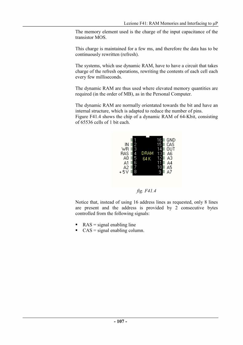
Lezione F41: RAM Memories and Interfacing to µP
- 107 -
The memory element used is the charge of the input capacitance of thetransistor MOS. This charge is maintained for a few ms, and therefore the data has to becontinuously rewritten (refresh). The systems, which use dynamic RAM, have to have a circuit that takescharge of the refresh operations, rewriting the contents of each cell eachevery few milliseconds. The dynamic RAM are thus used where elevated memory quantities arerequired (in the order of MB), as in the Personal Computer. The dynamic RAM are normally orientated towards the bit and have aninternal structure, which is adapted to reduce the number of pins. Figure F41.4 shows the chip of a dynamic RAM of 64-Kbit, consistingof 65536 cells of 1 bit each.
fig. F41.4
Notice that, instead of using 16 address lines as requested, only 8 linesare present and the address is provided by 2 consecutive bytescontrolled from the following signals: � RAS = signal enabling line� CAS = signal enabling column.

Lesson F41: RAM Memories and Interfacing to µP
- 108 -
F41.3 MEMORY RAM 6264 At the interior of Module Z3/EV the static memories RAM 6264 areused. They are memories which can contain up to a 64 Kbit of informationorganized in 8192 words of 8 byte ( 8 KB ). Require a single supply of +5V and are available in a standard packageof 28 pin, compatible with the EPROM memories. The main characteristics are indicated in the table: Internal configuration 8192 x 8 bit Supply + 5 Volt Active mode consumption 15 mW (1 MHz) Stand-by consumption 0.1 mW Access time 100-150 ns Inputs and outputs TTL
The internal block diagram and the pin-out are indicated in fig. F41.5 .
fig. F41.5 The timing for the reading operations is indicated in Fig. F41.6, whilethose for the writing operations is indicated in Fig. F41.7.
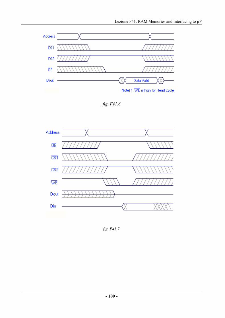
Lezione F41: RAM Memories and Interfacing to µP
- 109 -
fig. F41.6
fig. F41.7
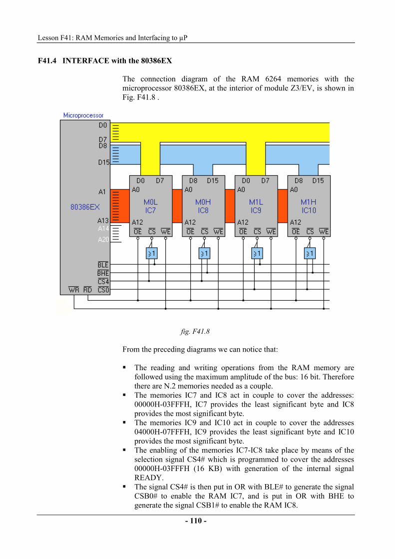
Lesson F41: RAM Memories and Interfacing to µP
- 110 -
F41.4 INTERFACE with the 80386EX
The connection diagram of the RAM 6264 memories with themicroprocessor 80386EX, at the interior of module Z3/EV, is shown inFig. F41.8 .
fig. F41.8
From the preceding diagrams we can notice that: � The reading and writing operations from the RAM memory are
followed using the maximum amplitude of the bus: 16 bit. Thereforethere are N.2 memories needed as a couple.
� The memories IC7 and IC8 act in couple to cover the addresses:00000H-03FFFH, IC7 provides the least significant byte and IC8provides the most significant byte.
� The memories IC9 and IC10 act in couple to cover the addresses04000H-07FFFH, IC9 provides the least significant byte and IC10provides the most significant byte.
� The enabling of the memories IC7-IC8 take place by means of theselection signal CS4# which is programmed to cover the addresses00000H-03FFFH (16 KB) with generation of the internal signalREADY.
� The signal CS4# is then put in OR with BLE# to generate the signalCSB0# to enable the RAM IC7, and is put in OR with BHE togenerate the signal CSB1# to enable the RAM IC8.

Lezione F41: RAM Memories and Interfacing to µP
- 111 -
� The enabling of the memories IC9-IC10 takes place by means ofselection signal CS1# which is programmed to cover the addresses04000H-07FFFH (16 KB) with generation of the internal signalREADY.
� The signal CS1# is then put in OR with BLE# to generate the signalCSB2# to enable the RAM IC9, and is put in OR with BHE togenerate the signal CSB3# to enable the RAM IC10.
� The enabling signal when during the writing WE# of the RAMmemories arrives directly from the writing signal WR# of themicroprocessor.
� The enabling signal when during the reading OE# of the RAMmemories arrives directly from the reading signal RD# of themicroprocessor.
� The address lines A0-A12 of the RAM memories are connected tothe address lines A1-A13 of the microprocessor.

Lesson F41: RAM Memories and Interfacing to µP
- 112 -
F41.5 EXERCISES and SUMMARY QUESTIONNAIRE
���� Z3
���� SIS1 Set all the switches in the OFF position
���� SIS2 Insert code Lesson: F41
We would like to develop a program for the Module Z3/EV that doesthe test of the memories RAM M1H and M1L. This program writesdata in the cells, then reads it and visualizes it on the display, one byteat a time, in a continuous and timed mode. The memories M1L and M1H are used because they are empty. Theprogram is in fact charged to address 00800 appertaining to memoriesM0L and M0H. In the contrary case, the writing of data on the RAMwould destroy the program. The list of the program is indicated next. 1 PAGE 70,166 2 ;----------------------- PRG_RAM -------------------- 3 ;writes code AA in each cell of the memories RAM 4 ;M1L and M1H,then reads the cells and visualizes the data 5 ;read on the display, each 1 s 6 = 0800 MEM_POS = 0800H 7 = 0080 DS_SEG = 0080H 8 = 0009 IDIS_BYTE = 09H ;interruption vis. byte 9 = 000B IDIS_STR = 0BH ;interruption vis. stringe 10 = 000D IWAIT_MS = 0DH ;interruption wait ms 11 ;---------------------------------------- CODE 12 ;program charged at address 0000:MEM_POS 13 0000 CODE SEGMENT 14 ASSUME CS:CODE, DS:CODE 15 0000 ORG 0H 16 0000 B8 0080 START: MOV AX,DS_SEG 17 0003 8E D8 MOV DS,AX ;charges data segment 18 0005 BE 0034 R MOV SI,OFFSET MSG 19 0008 CD 0B INT IDIS_STR ;display message MSG 20 000A B8 0400 MOV AX,0400H ;segment RAM 21 000D 8E C0 MOV ES,AX 22 000F BE 0000 MOV SI,0000H ;address RAM 23 0012 B0 AA TLOOP: MOV AL,0AAH 24 0014 26: 88 04 MOV ES:[SI],AL ;writes data in RAM 25 0017 26: 8A 04 MOV AL,ES:[SI] ;reads data from RAM 26 001A B1 0C MOV CL,12 27 001C CD 09 INT IDIS_BYTE ;visualizes data 28 001E 8B C MOV AX,SI 29 0020 8A C4 MOV AL,AH 30 0022 B1 05 MOV CL,5 31 0024 CD 09 INT IDIS_BYTE ; visualizes MSB ind. 32 0026 8B C6 MOV AX,SI 33 0028 B1 07 MOV CL,7 34 002A CD 09 INT IDIS_BYTE ; visualizes LSB ind. 35 002C B8 03E8 MOV AX,1000 36 002F CD 0D INT IWAIT_MS ;wait 37 0031 46 INC SI ;increments address 38 0032 EB DE JMP TLOOP 39 40 0034 52 41 4D 3A 20 78 MSG DB 'RAM: xxxx - xx ',00H 41 78 78 78 20 2D 20 42 78 78 20 20 00 43 44 0045 CODE ENDS 45 END START
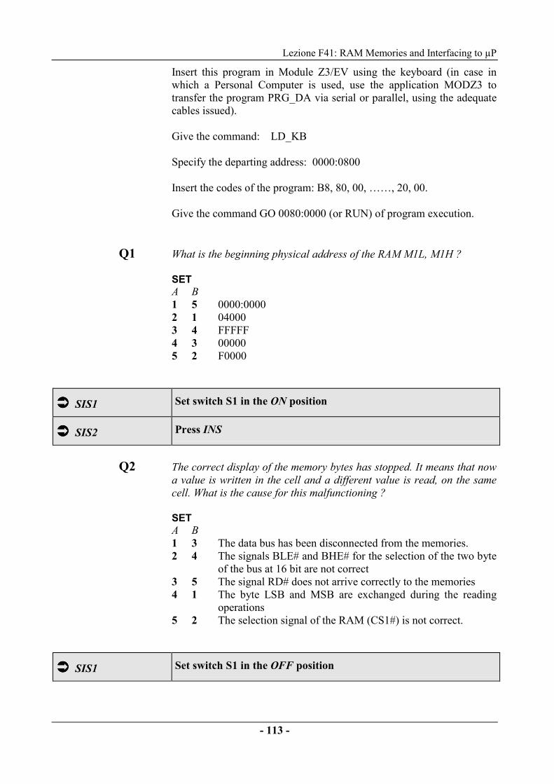
Lezione F41: RAM Memories and Interfacing to µP
- 113 -
Insert this program in Module Z3/EV using the keyboard (in case inwhich a Personal Computer is used, use the application MODZ3 totransfer the program PRG_DA via serial or parallel, using the adequatecables issued). Give the command: LD_KB Specify the departing address: 0000:0800 Insert the codes of the program: B8, 80, 00, ……, 20, 00. Give the command GO 0080:0000 (or RUN) of program execution.
Q1 What is the beginning physical address of the RAM M1L, M1H ? SETA B 1 5 0000:0000 2 1 04000 3 4 FFFFF4 3 000005 2 F0000
���� SIS1 Set switch S1 in the ON position
���� SIS2 Press INS
Q2 The correct display of the memory bytes has stopped. It means that now
a value is written in the cell and a different value is read, on the samecell. What is the cause for this malfunctioning ? SETA B1 3 The data bus has been disconnected from the memories.2 4 The signals BLE# and BHE# for the selection of the two byte
of the bus at 16 bit are not correct3 5 The signal RD# does not arrive correctly to the memories 4 1 The byte LSB and MSB are exchanged during the reading
operations 5 2 The selection signal of the RAM (CS1#) is not correct.
���� SIS1 Set switch S1 in the OFF position

Lesson F41: RAM Memories and Interfacing to µP
- 114 -
Q3 What are the signals which serve to enable the reading of the leastsignificant byte and the most significant one of the bus of 16 bit of themicroprocessor ? SETA B 1 4 Lines A0, A1 of the addresses 2 3 Lines BLE# and BHE# 3 2 Lines RD# and WR# 4 1 The different connection to the addresses bus.
Q4 How many address lines are used to read the data from the memoriesRAM 6364 ? SETA B 1 4 13 2 3 14 3 1 15 4 2 16.
Q5 How is the signal of READY generated, necessary for themicroprocessor to end the reading and writing operations with the RAMmemories? SETA B 1 4 Internally at the microprocessor 2 3 By means of the uphill front of the enabling signal CE# of the
memories 3 2 By means of the signal W/R# 4 1 By means of the most significant bit of the addresses.
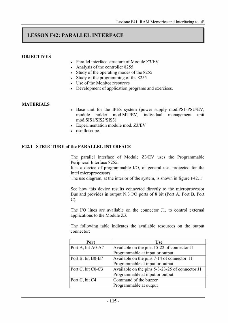
Lezione F41: RAM Memories and Interfacing to µP
- 115 -
LESSON F42: PARALLEL INTERFACE
OBJECTIVES• Parallel interface structure of Module Z3/EV• Analysis of the controller 8255• Study of the operating modes of the 8255• Study of the programming of the 8255• Use of the Monitor resources• Development of application programs and exercises.
MATERIALS
• Base unit for the IPES system (power supply mod.PS1-PSU/EV,module holder mod.MU/EV, individual management unitmod.SIS1/SIS2/SIS3)
• Experimentation module mod. Z3/EV• oscilloscope.
F42.1 STRUCTURE of the PARALLEL INTERFACE
The parallel interface of Module Z3/EV uses the ProgrammablePeripheral Interface 8255.It is a device of programmable I/O, of general use, projected for theIntel microprocessors.The use diagram, at the interior of the system, is shown in figure F42.1:
See how this device results connected directly to the microprocessorBus and provides in output N.3 I/O ports of 8 bit (Port A, Port B, PortC).
The I/O lines are available on the connector J1, to control externalapplications to the Module Z3.
The following table indicates the available resources on the outputconnector:
Port UsePort A, bit A0-A7 Available on the pins 15-22 of connector J1
Programmable at input or outputPort B, bit B0-B7 Available on the pins 7-14 of connector J1
Programmable at input or outputPort C, bit C0-C3 Available on the pins 5-3-23-25 of connector J1
Programmable at input or outputPort C, bit C4 Command of the buzzer
Programmable at output
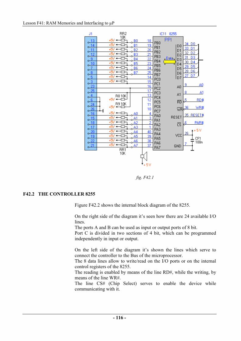
Lesson F41: RAM Memories and Interfacing to µP
- 116 -
fig. F42.1
F42.2 THE CONTROLLER 8255
Figure F42.2 shows the internal block diagram of the 8255.
On the right side of the diagram it’s seen how there are 24 available I/Olines.The ports A and B can be used as input or output ports of 8 bit.Port C is divided in two sections of 4 bit, which can be programmedindependently in input or output.
On the left side of the diagram it’s shown the lines which serve toconnect the controller to the Bus of the microprocessor.The 8 data lines allow to write/read on the I/O ports or on the internalcontrol registers of the 8255.The reading is enabled by means of the line RD#, while the writing, bymeans of the line WR#.The line CS# (Chip Select) serves to enable the device whilecommunicating with it.
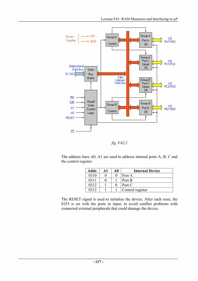
Lezione F41: RAM Memories and Interfacing to µP
- 117 -
fig. F42.2
The address lines A0, A1 are used to address internal ports A, B, C andthe control register:
Addr. A1 A0 Internal Device0310 0 0 Port A0311 0 1 Port B0312 1 0 Port C0313 1 1 Control register
The RESET signal is used to initialize the device. After each reset, the8255 is set with the ports in input, to avoid conflict problems withconnected external peripherals that could damage the device.
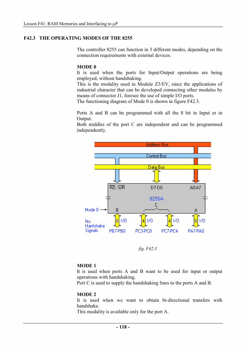
Lesson F41: RAM Memories and Interfacing to µP
- 118 -
F42.3 THE OPERATING MODES OF THE 8255
The controller 8255 can function in 3 different modes, depending on theconnection requirements with external devices.
MODE 0It is used when the ports for Input/Output operations are beingemployed, without handshaking.This is the modality used in Module Z3/EV, since the applications ofindustrial character that can be developed connecting other modules bymeans of connector J1, foresee the use of simple I/O ports.The functioning diagram of Mode 0 is shown in figure F42.3.
Ports A and B can be programmed with all the 8 bit in Input or inOutput.Both middles of the port C are independent and can be programmedindependently.
fig. F42.3
MODE 1It is used when ports A and B want to be used for input or outputoperations with handshaking.Port C is used to supply the handshaking lines to the ports A and B.
MODE 2It is used when we want to obtain bi-directional transfers withhandshake.This modality is available only for the port A.
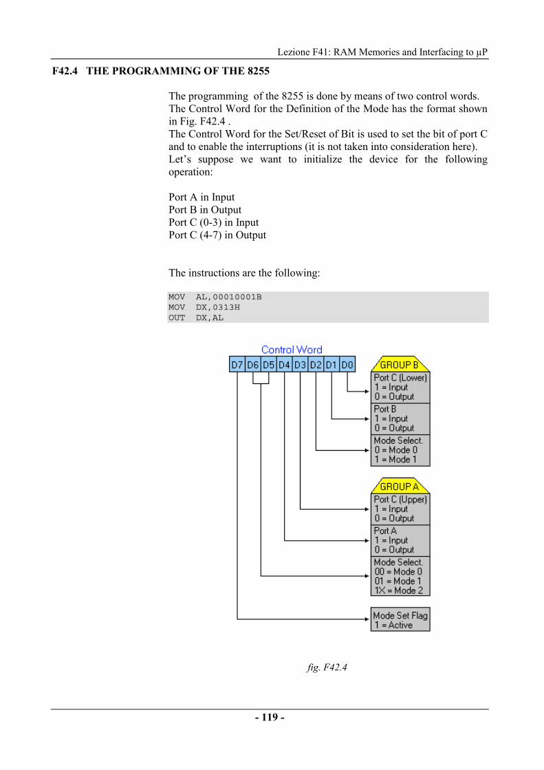
Lezione F41: RAM Memories and Interfacing to µP
- 119 -
F42.4 THE PROGRAMMING OF THE 8255
The programming of the 8255 is done by means of two control words.The Control Word for the Definition of the Mode has the format shownin Fig. F42.4 .The Control Word for the Set/Reset of Bit is used to set the bit of port Cand to enable the interruptions (it is not taken into consideration here).Let’s suppose we want to initialize the device for the followingoperation:
Port A in InputPort B in OutputPort C (0-3) in InputPort C (4-7) in Output
The instructions are the following:
MOV AL,00010001BMOV DX,0313HOUT DX,AL
fig. F42.4
Lesson F41: RAM Memories and Interfacing to µP
- 120 -
F42.5 USE of the MONITOR’S RESOURCES
It was seen previously the programming of the 8255.This mode of proceeding can be simplified using the softwareinterruptions of the system’s Monitor, actually made for this purpose.The system’s Monitor contains in fact the following softwareinterruptions for the management of this interface:
� INT 10H: use of the buzzer� INT 12H: programming, writing and reading data on ports A, B, C
INT 10HCommand of the Buzzer.This interruption commands the emission of sounds on the buzzer.It’s possible to specify the frequency and the duration of the emittedsounds.
INPUT BX = durationCX = frequency
OUTPUT noneAlteredRegisters
none
INT 12HManagement of the Parallel Interface.This interruption manages the functioning of the parallel interface.The controller 8255 is always used in Mode 0 (Basic I/O).The available functions are determined from the contents of AH:
INPUT AH = 0 Programming portsAH = 1 Sending data to port AAH = 2 Sending data to port BAH = 3 Sending data to port CAH = 4 Reading data from port AAH = 5 Reading data from port BAH = 6 Reading data from port C
OUTPUT AL = data readAlteredRegisters
none
AH = 0 : Programming portsThe contents of AL determines the direction (I/O) of the ports:
Register AL ProgrammingBit 0 = 0 : port A in output
= 1 : port A in inputBit 1 = 0 : port B in output
= 1 : port B in inputBit 2 = 0 : port C (C0-C3) in output
= 1 : port C (C0-C3) in input

Lezione F41: RAM Memories and Interfacing to µP
- 121 -
AH = 1, 2, 3 : Sending Data to ports A, B, CThe contents of AL determines the data to be sent to the ports.
AH = 4, 5, 6 : Reading Data from ports A, B, CThe contents of AL in output corresponds to data read from the port.

Lesson F41: RAM Memories and Interfacing to µP
- 122 -
F42.6 EXERCISES and SUMMARY QUESTIONNAIRE
���� Z3
���� SIS1 Set all switches in the OFF position
���� SIS2 Insert code Lesson: F42
We would like to develop a program for the Module Z3/EV thatcommands in a cyclic timed mode the bit of the ports A and B, andemits one beep at each change of state. The list of the program is indicated next. 1 PAGE 70,166 2 ;--------------------- PRG_PAR ---------------------- 3 ; cyclic timed command of the bits of the Ports A/B and 4 ;generation of a 'beep' at each change of state 5 = 0800 MEM_POS = 0800H 6 = 0080 DS_SEG = 0080H 7 = 000D IWAITMS = 0DH ;wait interruption 8 = 0010 IBUZZER = 10H ;interruption buzzer command 9 = 0012 IPARAL = 12H ;interruption parallel control 10 11 ;---------------------------------------- CODE 12 ;program charged in address 0000:MEM_POS 13 0000 CODE SEGMENT 14 ASSUME CS:CODE, DS:CODE 15 0000 ORG 0H 16 0000 B8 0080 START: MOV AX,DS_SEG 17 0003 8E D8 MOV DS,AX ;charges data segment 18 0005 B4 00 MOV AH,00H 19 0007 B0 00 MOV AL,00H 20 0009 CD 12 INT IPARAL ;ports in Output 21 000B B3 01 MOV BL,00000001B ;data out 22 000D B4 01 LOOP1: MOV AH,1 23 000F 8A C3 MOV AL,BL 24 0011 CD 12 INT IPARAL ;command port A 25 0013 B4 02 MOV AH,2 26 0015 8A C3 MOV AL,BL 27 0017 CD 12 INT IPARAL ;command port B 28 0019 53 PUSH BX 29 001A BB 0014 MOV BX,20 30 001D B9 000A MOV CX,10 31 0020 CD 10 INT IBUZZER ;beep 32 0022 5B POP BX 33 0023 B8 03E8 MOV AX,700 34 0026 CD 0D INT IWAITMS 35 0028 D0 E3 SHL BL,1 ;shifts bit to left 36 002A 80 FB 00 CMP BL,00H 37 002D 75 DE JNZ LOOP1 38 002F B3 01 MOV BL,00000001B 39 0031 EB DA JMP LOOP1 40 41 0033 CODE ENDS 42 END START
Insert this program in Module Z3/EV using the keyboard (in case inwhich a Personal Computer is used, use the application MODZ3 totransfer the program PRG_PAR via serial or parallel, using the adequatecables issued). Give the command: LD_KB

Lezione F41: RAM Memories and Interfacing to µP
- 123 -
Specify the departing address: 0000:0800 Insert the codes of the program as listed Give the command GO 0080:0000 (or RUN) of program execution.
Q1 What is the total time of the bit ignition cycle? SETA B 1 3 5s 2 5 1s 3 1 10s4 2 20s5 4 2s
���� SIS1 Set switch S10 in the ON position
���� SIS2 Press INS
Q2 It can be observed now how one of the bit is not activated. which one is
this bit ? SETA B1 5 A52 4 B23 1 A7 4 2 A0 5 3 B0
Q3 What is the cause of this malfunctioning ? SETA B1 2 The data bus doesn’t result to be correctly connected to the
controller 8255 anymore2 3 The output line A0 of the 8255 is connected to ground3 4 The output line A7 of the 8255 is connected to ground 4 5 The line A0 is in short-circuit with the line A1 5 1 The controller 8255 isn’t programmed correctly anymore.
Lesson F41: RAM Memories and Interfacing to µP
- 124 -
���� SIS1 Set switch S10 in the OFF position
Set switch S12 in the ON position
���� SIS2 Press INS
Q4 It can be observed now how one of the bit is not activated. which one is
this bit ? SETA B1 3 B52 4 B23 1 A7 4 5 A0 5 1 B0
Q5 What is the cause of this malfunctioning ? SETA B1 2 The data bus doesn’t result to be correctly connected to the
controller 8255 anymore2 1 The line di output B5 of the 8255 is connected to ground3 5 The output line A6 of the 8255 is connected to ground 4 3 The line B5 is in short-circuit with the line B6 5 4 The controller 8255 isn’t programmed correctly anymore.
���� SIS1 Set switch S12 in the OFF position
Q6 What’s the finality of the instruction PUSH BX at the interior of theprogram (the instruction shows up one time only) ? SETA B 1 4 Charge BX with a new value 2 3 Pass BX as a parameter at interruption IBUZZER 3 2 Transfer BX to another register 4 1 Save temporarily the value of BX.

Lezione F41: RAM Memories and Interfacing to µP
- 125 -
Q7 What is the word of 16 bit which has to be charged into register AX to
program port A in input, port B in output and port C0-C3 in input, bymeans of the interruption INT 12H ? SETA B 1 2 00000000 00000101 2 1 00000001 00000101 3 4 00000000 00000010 4 3 00000001 00000010

NOTE


ELETTRONICA VENETA spa - 31045 Motta di Livenza (Treviso) ITALYVia Postumia. 16 – Tel. +39 0422 7657 r.a. – Fax +39 0422 861901www.elettronicaveneta.com
All rights reserved. No part of this publication may be reproduced, stored in any retrieval system, or transmitted in any form or by anymeans, electronic, mechanical, photocopying, recording, or otherwise without the prior writen permission of Elettronica Veneta S.p.a.