zener diodes and applications zener diodes
TRANSCRIPT
University of Thi-QarElectrical and Electronic Engineering Department lecture Seven Second year, Electronic ɪ, 2016-2017 by: Abdulgaffar S. M.
Zener Diodes and Applications
Zener Diodes:
Diodes which are designed with plate power-dissipation capabilities to operate in the breakdown region may be employed as voltage-reference or constant-voltage devices. Such are known as avalanche, breakdown, or zener diodes. The zener diode is made for operation in the breakdown region. By varying the doping level, a manufacturer can produce zener diodes with breakdown voltages from 2 to 250V.
When the applied reverse voltage reaches the breakdown value, minority carries in the depletion layer are accelerated and reach high enough velocities to dislodge valence electrons from outer orbits. The newly liberated electrons can then gain high enough velocities to free other valence electrons. In this way, we get an avalanche of free electrons. Avalanche occurs for reverse voltages greater than 6V or so.
The zener effect is different. When a diode is heavily doped, the depletion layer is very narrow. Because of this, the electric field across the depletion layer is very intense. When
the field strength reaches approximately 3× 10⁷ V/m, the field is intense enough to pull
electrons out of valence orbits. The creation of free electrons in this way is called zener breakdown (also known as high-field emission).
The zener effect is predominant for breakdown voltages less than 4V, the avalanche effectis predominant for breakdown voltages greater than 6V, and both effect are present between 4 and 6V. originally, people thought the zener effect was the only breakdown mechanism in diodes. For this reason, the name "zener diode" came into widespread use before the avalanche effect was discovered. All diodes optimized for operation in the breakdown region are therefore still called zener diodes.
1
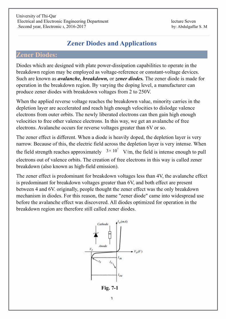
Fig. 7-1
University of Thi-QarElectrical and Electronic Engineering Department lecture Seven Second year, Electronic ɪ, 2016-2017 by: Abdulgaffar S. M.
Fig. 7-1 shows the schematic symbol and the current-voltage curve of a zener diode.
Negligible reverse current flows until we reach the breakdown voltage V Z . In a zener
diode, the breakdown has a very sharp knee, followed by an almost vertical increase in
current. Note that the voltage is approximately constant, equal to V Z over most of
breakdown region. Data sheets usually the value of V Z at a particular knee currentI ZK which is beyond the knee (see Fig. 7-1).
The power dissipation of a zener diode equals the product of its voltage and current. In symbols,
PZ=V Z . I Z
As long as PZ is less than the power rating max¿
Z¿P¿
, the zener diode will not be
destroyed. Commercially available zener diodes have power ratings from 0.25W to more than 50W. Data sheets often specify the maximum current a zener diode can handle
without exceeding its power rating. This maximum current is designed max¿
Z¿I¿
(see
Fig.7-1).
The relation between max¿
Z¿I¿
and power rating is given by
max¿¿
max¿¿
Z¿P¿
Z¿I¿
When a zener diode is operating in the breakdown region, a small increase in voltage produces a large increase in current. This implies that a zener diode has a small dynamic
resistance ( r Z , see Fig. 7-1). We can calculate this zener resistance by
r Z=∆ v∆i
2
University of Thi-QarElectrical and Electronic Engineering Department lecture Seven Second year, Electronic ɪ, 2016-2017 by: Abdulgaffar S. M.
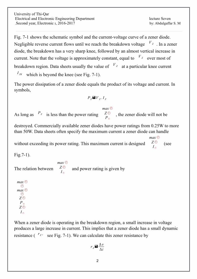
The complete equivalent circuit of the zener diode in the zener region includes a small
dynamic resistancer
(¿¿Z)¿
and dc battery equal to the zener potential V
(¿¿Z)¿
,
as shown in Fig. 7-2a. for all applications to follow, however, we shall assume as a first approximation that the external resistance are much larger in magnitude than the zener-equivelent resistor and that the equivalent circuit is simply the dc battery that equal to
V(¿¿Z)
¿ as indicated in Fig. 7-2b.
Zener Diode:
these diodes have adequate power dissipation capabilities to operate in the breakdown region. These are used as voltage reference, and constant voltage devices. These are called avalanche, breakdown or zener diodes.
Zener may have breakdown voltage 2 to 200V depending upon level of doping.
3
Fig. 7-1
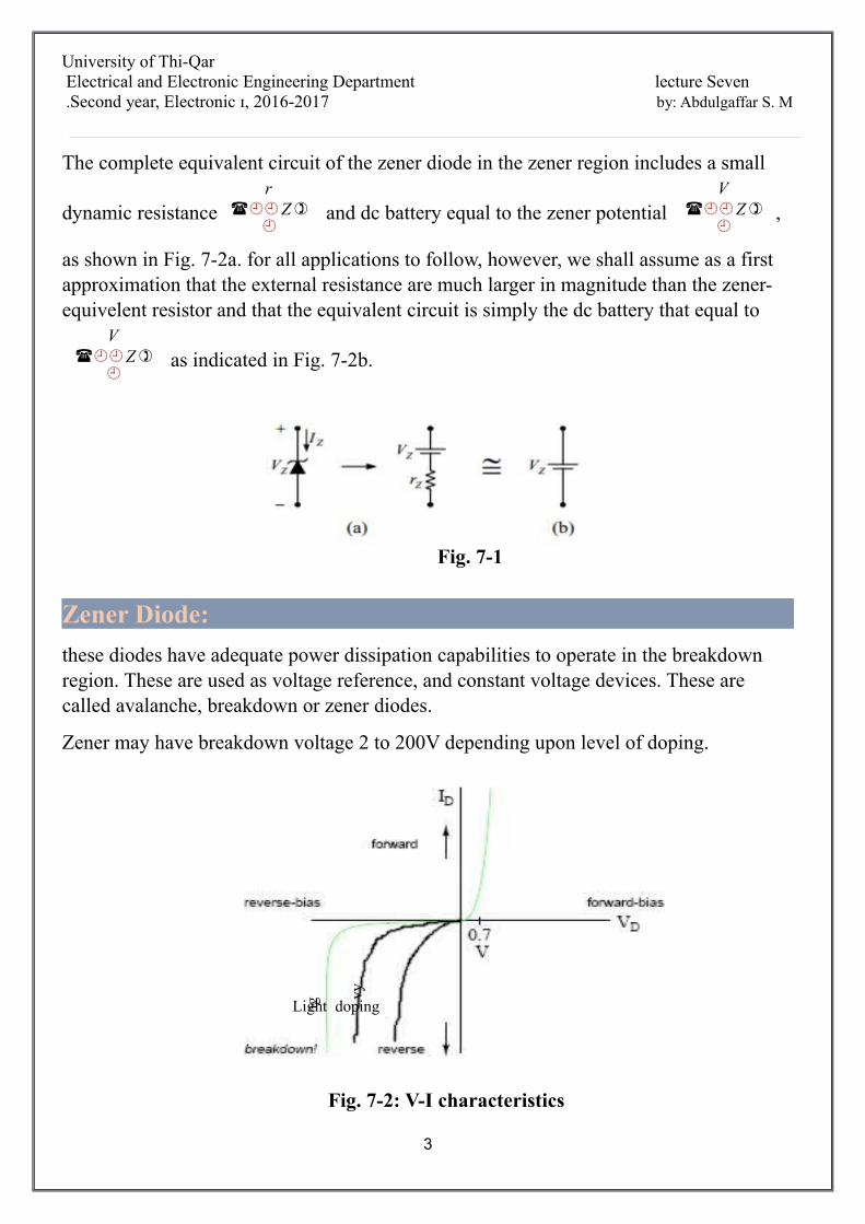
Fig. 7-2: V-I characteristics
Hea
vy d
opin
g Light doping
Ver
y he
avy
University of Thi-QarElectrical and Electronic Engineering Department lecture Seven Second year, Electronic ɪ, 2016-2017 by: Abdulgaffar S. M.
Avalanche Breakdown:
When the applied reverse voltage reaches the breakdown value, minority carriers in the depletion layer are accelerated and reach high enough velocity to dislodge valance electrons from outer orbits. These newly liberate electrons further free valence electrons. In this way avalanche of free electrons is obtained. Avalanche occurs for reverse voltage greater than 6V.
Zener Breakdown:
With heavily doping the depletion layer becomes narrow and electric field intensity across the depletion layer is very intense of the order of 300KV/cm, enough to pull electrons out of valance orbits. The free electron creation of this way is called zener breakdown or high field emission.
This effect is prominent for breakdown voltages less than 4V.
Both avalanche and zener effect are present between 4V and 6V.
Zener impedance:
Z Z=∆ v∆ i
→ called dynamic impedance
In breakdown region, zener diode has small impedance in voltage produces large chang in current. The change in zener voltage with temp.
∆V Z=T C × ∆T × V Z
Where
T C : temperturecoefficient
∆T : change∈temp .
V Z : zener voltage
Then
T C=∆V Z /V Z
T 1− T o
× 100 C °
Where 4
University of Thi-QarElectrical and Electronic Engineering Department lecture Seven Second year, Electronic ɪ, 2016-2017 by: Abdulgaffar S. M.
T 1 : is the new temperature level
T o : is room temperature in an enclosed cabinet ( 25C ° )
T C : is thetemperture coefficient
V Z : is the nominal zener potential at 25 C °
Example7-1:
Analyze the 10V zener diode if the zener diode if the temperature is increased to100 C ° and typical temperature coefficient is 0. 0.072C ° .
Solution:
∆V Z=T C ×V Z
100 (T 1−T o)=(0.072 %C °)(10V )100 (100−25)C °
∆V Z=0.54V
The resulting potential zener is now
V Z=V Z+0.54=10.54 V
The power dissipation of zener diode PZ=V Z . I Z
The maximum current in zener
max¿¿
max¿¿
Z¿P¿
Z¿I¿
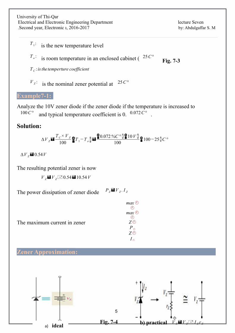
Zener Approximation:
5
Fig. 7-3
a) ideal b) practical ´V Z=V Z+ I Z r ZFig. 7-4
University of Thi-QarElectrical and Electronic Engineering Department lecture Seven Second year, Electronic ɪ, 2016-2017 by: Abdulgaffar S. M.
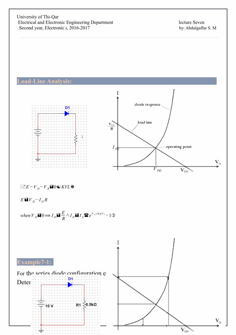
Load-Line Analysis:
+E−V D−V R=0[KVL]
E=V D−I D R
when V D=0⟹ I D=ER∧I D= I S(eV D/η V T−1)
Example7-1:
For the series diode configuration employing the diode characteristic.
Determine a) V DQ and I DQ b) V R
6
V R
I DQ
V DQ
University of Thi-QarElectrical and Electronic Engineering Department lecture Seven Second year, Electronic ɪ, 2016-2017 by: Abdulgaffar S. M.
a) I D=ER| , at V D=0⟹ I D=
10V0.5 k Ω
=20mA
V D=E at I D=0⟹ V D=10 V V DQ=0.78 V I DQ=18.5 mA
b) V R= I R R=(18.5mA) (1 k Ω )=18.5 V
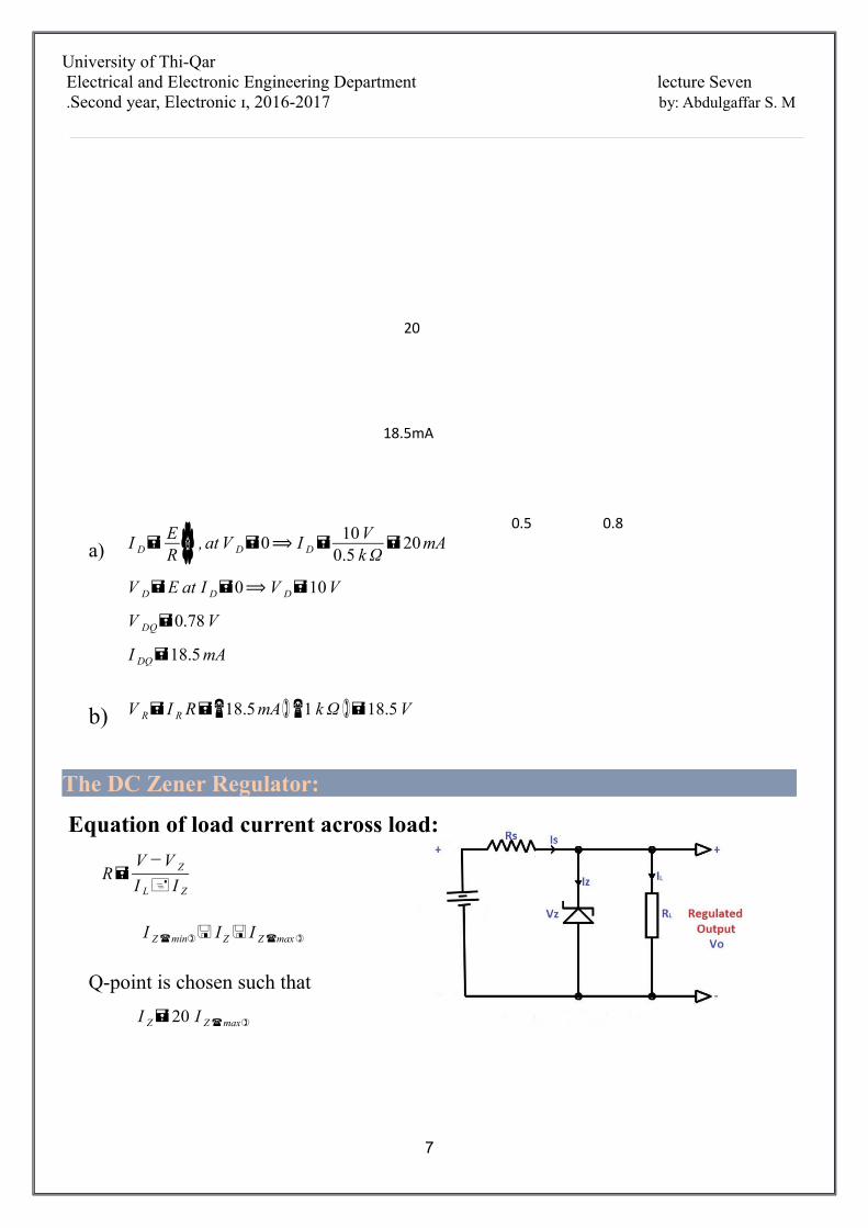
The DC Zener Regulator:
Equation of load current across load:
R=V−V Z
I L+ I Z
I Z(min)< I Z< I Z(max)
Q-point is chosen such that
I Z=20 I Z(max)
7
20
18.5mA
0.5 0.8
University of Thi-QarElectrical and Electronic Engineering Department lecture Seven Second year, Electronic ɪ, 2016-2017 by: Abdulgaffar S. M.
max¿¿
Z ¿I L+0.2 I¿∴R=
V−V Z
¿
And
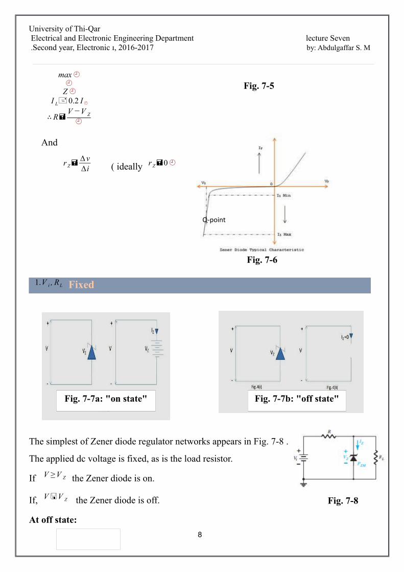
r Z=∆ v∆i ( ideally r Z=0¿
1.V i , RL Fixed
The simplest of Zener diode regulator networks appears in Fig. 7-8 .
The applied dc voltage is fixed, as is the load resistor.
If V ≥ V Z the Zener diode is on.
If, V <V Z the Zener diode is off.
At off state:
8
Fig. 7-5
Fig. 7-6
Q-point
Fig. 7-7a: "on state" Fig. 7-7b: "off state"
Fig. 7-8
University of Thi-QarElectrical and Electronic Engineering Department lecture Seven Second year, Electronic ɪ, 2016-2017 by: Abdulgaffar S. M.
V =V L=V i Rl
RL+R
At on state:
V L=V Z
I R= I Z + I L
I Z= I R−I L , I L=V L
RL & I R=
V R
R=
V i−V Z
R
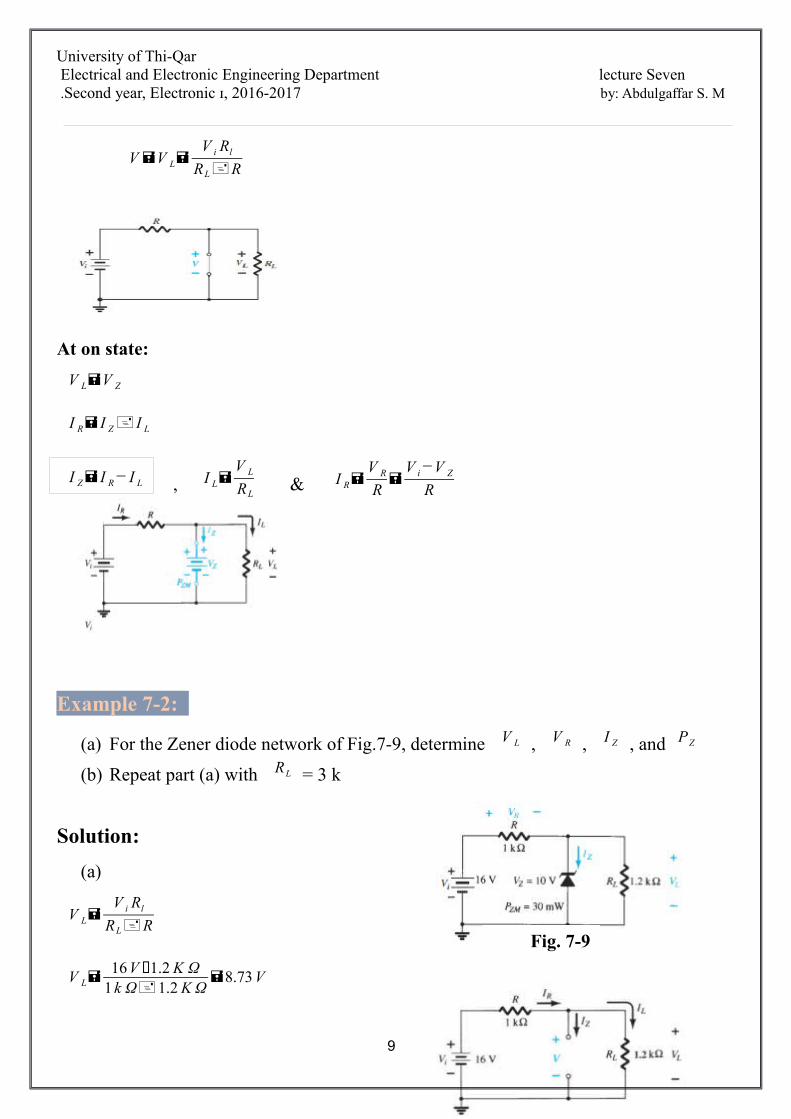
Example 7-2:
(a) For the Zener diode network of Fig.7-9, determine V L , V R , I Z , and PZ
(b) Repeat part (a) with RL = 3 k
Solution:
(a)
V L=V i Rl
RL+R
V L=16V ∗1.2 K Ω
1k Ω+1.2 K Ω=8.73 V
9
Fig. 7-9
University of Thi-QarElectrical and Electronic Engineering Department lecture Seven Second year, Electronic ɪ, 2016-2017 by: Abdulgaffar S. M.
V L=V =8.73V
I Z=0
V R=V i− V L=16− 8.73=7.72 V
PZ=V Z . I Z=0W
(b)
V =V i Rl
RL+R=
16∗31+3
=12V
Since V=12V is greater than V Z=10, the diode is in the "on state". Then :
V L=V Z=10 V
V R=V i−V Z=16−10=6V
I L=V Z
RL
=103=3.33 mA
I R=V R
R=
61=6 MA
I Z= I R− I L=6mA− 3.33 mA=2.67 mA
PZ=V Z . I Z=10∗2.67=26.7 mW
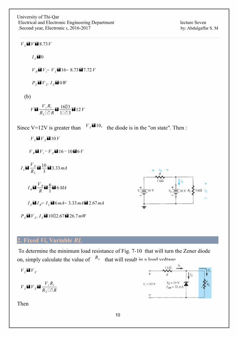
2. Fixed Vi, Variable RL
To determine the minimum load resistance of Fig. 7-10 that will turn the Zener diode
on, simply calculate the value of RL that will result in a load voltage
V L=V Z
V L=V Z=V i Rl
RL+R
Then
10
University of Thi-QarElectrical and Electronic Engineering Department lecture Seven Second year, Electronic ɪ, 2016-2017 by: Abdulgaffar S. M.
min¿¿
L¿R¿
Any load resistance value greater than the min¿L¿R¿
that the Zener diode is in the “on”
state and the diode can be replaced by its V Z source equivalent.
max¿¿
min¿¿L¿R¿
L¿I¿
The diode is in the "on state & V R is fixed ( V R=V i− V Z¿ and I R remains fixed at
I R=V R
R .
Then
I Z= I R−I L
Minimum I Z when I L maximum , I R constant .
Maximum I Z when I L minimum , I R constant .
I L (min)= I R− I Z(max)
RL(min)=V Z
I L (min)
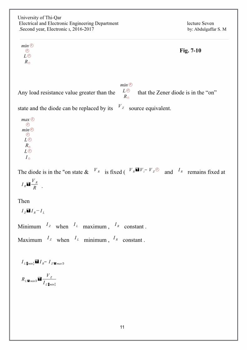
11
Fig. 7-10
University of Thi-QarElectrical and Electronic Engineering Department lecture Seven Second year, Electronic ɪ, 2016-2017 by: Abdulgaffar S. M.
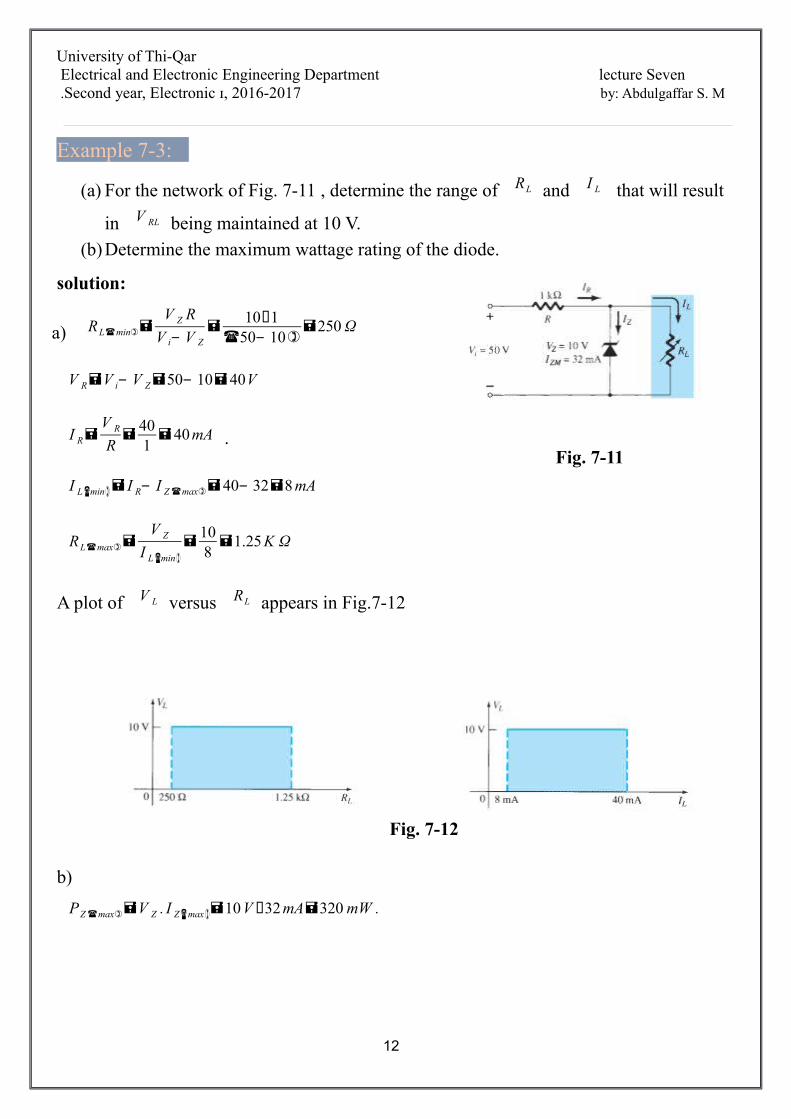
Example 7-3:
(a) For the network of Fig. 7-11 , determine the range of RL and I L that will result
in V RL being maintained at 10 V.
(b)Determine the maximum wattage rating of the diode.
solution:
a) RL(min)=V Z R
V i− V Z
=10∗1
(50− 10)=250 Ω
V R=V i− V Z=50− 10=40V
I R=V R
R=
401=40 mA .
I L (min)= I R− I Z(max)=40− 32=8 mA
RL(max)=V Z
I L (min)=
108=1.25 K Ω
A plot of V L versus RL appears in Fig.7-12
b)
PZ(max)=V Z . I Z (max)=10V ∗32mA=320 mW .
12
Fig. 7-11
Fig. 7-12
University of Thi-QarElectrical and Electronic Engineering Department lecture Seven Second year, Electronic ɪ, 2016-2017 by: Abdulgaffar S. M.
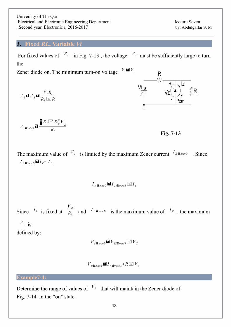
3. Fixed RL, Variable Vi
For fixed values of RL in Fig. 7-13 , the voltage V i must be sufficiently large to turn
the
Zener diode on. The minimum turn-on voltage V i=V i(min) is determined by:
V L=V Z=V i Rl
RL+R
V i(min)=(RL+R)V
Z
Rl
The maximum value of V i is limited by the maximum Zener current I Z(max) . SinceI Z(max)= I R− I L
I R(max)= I Z(max)+ I L
Since I L is fixed at V Z
RL and I Z(max) is the maximum value of I Z , the maximum
V i is
defined by:
V i(max)=V R(max)+V Z
V i(max)= I R(max)∗R+V Z
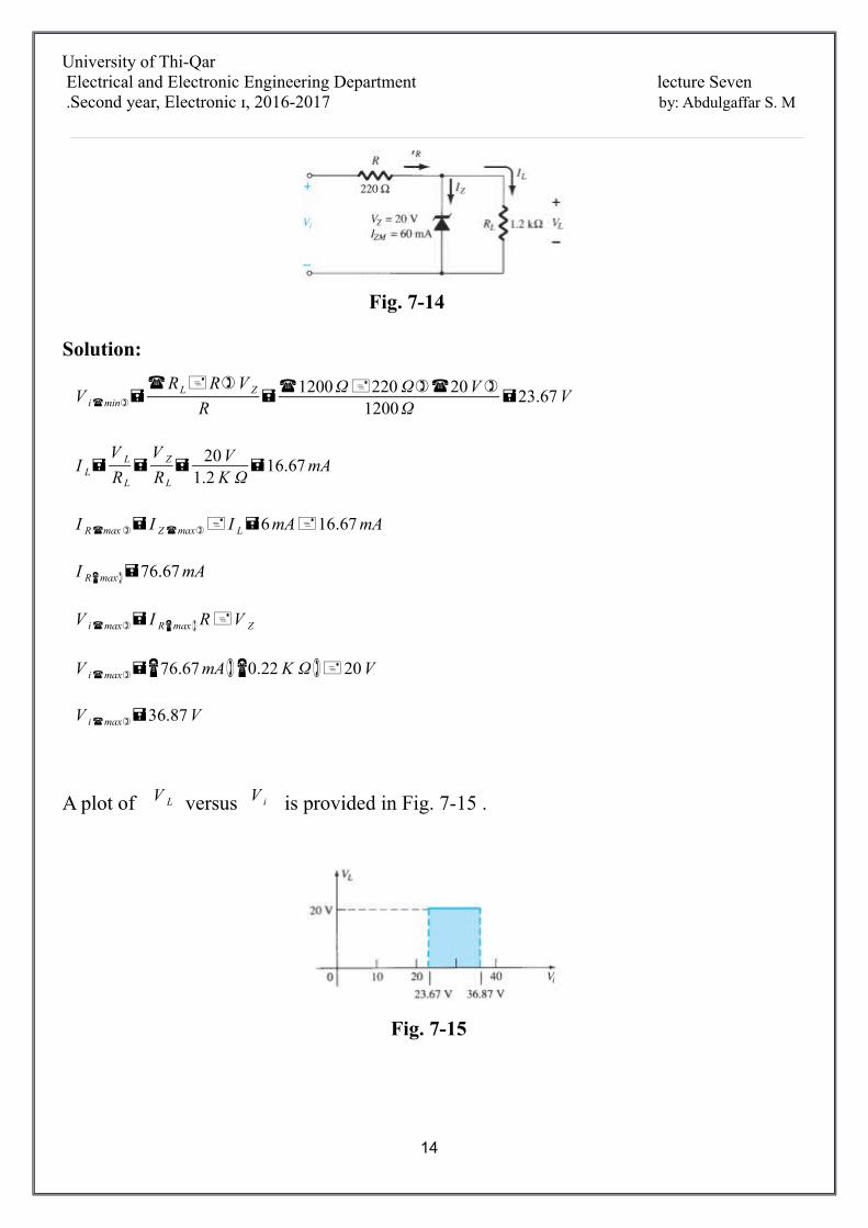
Example7-4:
Determine the range of values of V i that will maintain the Zener diode of
Fig. 7-14 in the “on” state.
13
Fig. 7-13
University of Thi-QarElectrical and Electronic Engineering Department lecture Seven Second year, Electronic ɪ, 2016-2017 by: Abdulgaffar S. M.
Solution:
V i(min)=(RL+R)V Z
R=(1200 Ω+220 Ω)(20V)
1200 Ω=23.67 V
I L=V L
RL
=V Z
RL
=20V
1.2 K Ω=16.67 mA
I R(max)= I Z(max)+ I L=6 mA+16.67 mA
I R(max)=76.67 mA
V i(max)= I R(max) R+V Z
V i(max)=(76.67 mA)(0.22 K Ω)+20 V
V i(max)=36.87 V
A plot of V L versus V i is provided in Fig. 7-15 .
14
Fig. 7-14
Fig. 7-15
University of Thi-QarElectrical and Electronic Engineering Department lecture Seven Second year, Electronic ɪ, 2016-2017 by: Abdulgaffar S. M.
Rectifiers
It has convert ac waveform to dc signal. The process of conversion is called rectification.
Types:
1. Half-Wave Rectifier.2. Full-Wave Rectifier.
a. Full-Wave Bridge Rectifier.b. Center-Tapped Transformer.
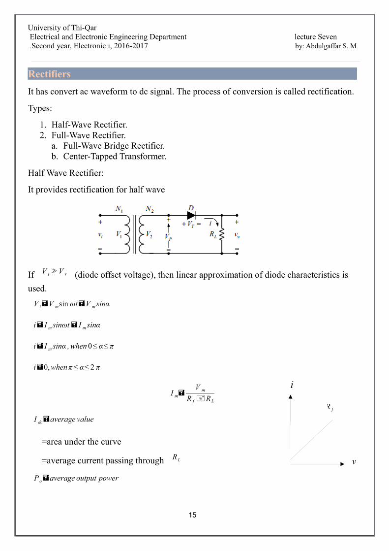
Half Wave Rectifier:
It provides rectification for half wave
If V i≫V r (diode offset voltage), then linear approximation of diode characteristics is
used.
V i=V msin ωt=V m sinα
i= I m sinωt= I m sinα
i= I m sinα ,when 0≤ α≤ π
i=0, when π ≤ α≤ 2 π
I m=V m
R f +RL
I dc=average value
=area under the curve
=average current passing through RL
Po=average output power
15
i
v
R f
University of Thi-QarElectrical and Electronic Engineering Department lecture Seven Second year, Electronic ɪ, 2016-2017 by: Abdulgaffar S. M.
Po=V dc=I m
πRL .
I m
π=(
I m
π)
2
. RL
Efficiency of rectification
I m
I¿
rms¿¿¿¿¿
(¿¿π)2 .RL
¿
η=Po
P i
=¿
I m
I¿¿m¿2
¿¿¿¿¿¿
(¿¿π)2.RL
¿η=¿
For RL≫R f∨ R f =0 , η=4
π 2⇒η percent=
4
π 2∗100 =40.6
Peak inverse voltage (PIV):
For every diode, these is a maximum voltage to which it can be subjected. It called peak inverse voltage (PIV).
PIV ≥ V m
16
I m R f sin ωt
University of Thi-QarElectrical and Electronic Engineering Department lecture Seven Second year, Electronic ɪ, 2016-2017 by: Abdulgaffar S. M.
Regulation:
The regulator is defined in percentage.
Regulation=V No load− V Full load
V Full load
∗100
- At no load V dc=V m
π .
- At full load V dc=− I dc . R f +V m
π=
V m
π− I dc . R f
Example 7-5 :
Find the regulation for the following circuit V Noload=12 V .
Solution:
V Full load=12− 0.1∗20
¿V dc− I dc . R f
= 12-2
=10V
%Req=12− 10
10∗100 =20
Ripple factor (r) :
It is a measure of fluctu ability component (ac component) and is definded as:
r=rms value of ac wave
average value of wave=
I rms
I dc
=V rms
V dc
Where ´I rms and
´V rms denote the rms value of ac component in current and voltage
respectively.
17
University of Thi-QarElectrical and Electronic Engineering Department lecture Seven Second year, Electronic ɪ, 2016-2017 by: Abdulgaffar S. M.
´i =i− I dc
i− I dc
¿1
2 π¿0
25°¿
¿¿¿
∴´
I rms¿
i(¿¿2− 2 I dc i+ I dc
2)dα1
2 π¿0
25 °¿
¿¿¿¿
= [ I rms2− I dc
2]12
∴r=√( I rms
I dc )2
− 1
For half wave rectifier (HWR)
I rms
I dc
=I m/2
I m/ π=
π2=1.57
∴r=√(1.57)2− 1=1.21
The result indicates that the rms ripple factor voltage exceeds the dc output voltage in HWR. It is poor circuit for converting ac to dc
Note:
min¿¿
L¿R¿
18
University of Thi-QarElectrical and Electronic Engineering Department lecture Seven Second year, Electronic ɪ, 2016-2017 by: Abdulgaffar S. M.
V R=0⇒V NL− V FL ≈ 0
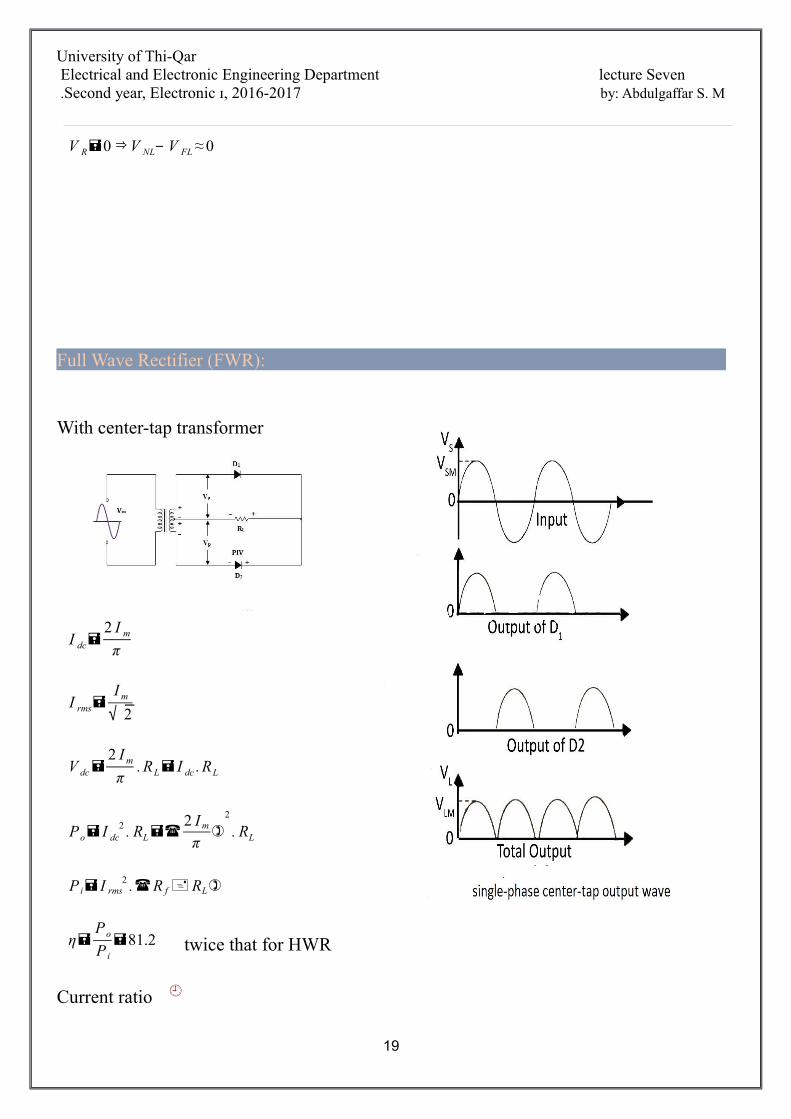
Full Wave Rectifier (FWR):
With center-tap transformer
I dc=2 I m
π
I rms=I m
√ 2
V dc=2 I m
π.RL= I dc .RL
Po= I dc2 . RL=(
2 I m
π)
2
. RL
P i= I rms2 .(R f +RL)
η=Po
P i
=81.2 twice that for HWR
Current ratio ¿
19
University of Thi-QarElectrical and Electronic Engineering Department lecture Seven Second year, Electronic ɪ, 2016-2017 by: Abdulgaffar S. M.
I rms
I dc
=I m/√ 2
2 I m/π =1.11
Ripple factor r=√ (1.11)2− 1=0.482
So ripple factor has dropped from 1.21 in HWR to 0.482 in FWR.
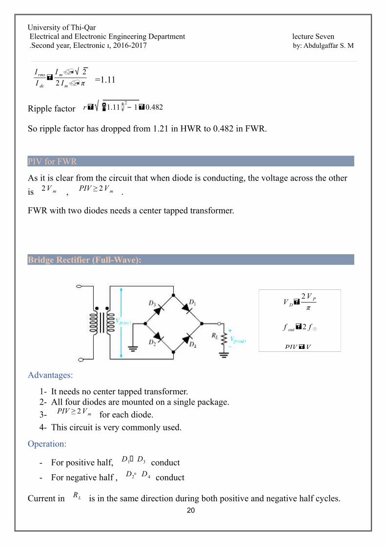
PIV for FWR
As it is clear from the circuit that when diode is conducting, the voltage across the other
is 2V m , PIV ≥ 2V m .
FWR with two diodes needs a center tapped transformer.
Bridge Rectifier (Full-Wave):
Advantages:
1- It needs no center tapped transformer.2- All four diodes are mounted on a single package.
3- PIV ≥ 2 V m for each diode.
4- This circuit is very commonly used.
Operation:
- For positive half, D1∧ D3 conduct
- For negative half , D2∧ D4 conduct
Current in RL is in the same direction during both positive and negative half cycles.20
V D=2 V P
π
f out=2 f ¿
PIV =V m
University of Thi-QarElectrical and Electronic Engineering Department lecture Seven Second year, Electronic ɪ, 2016-2017 by: Abdulgaffar S. M.
I dc=2 I m
π
V dc=2V m
π=0.636V m
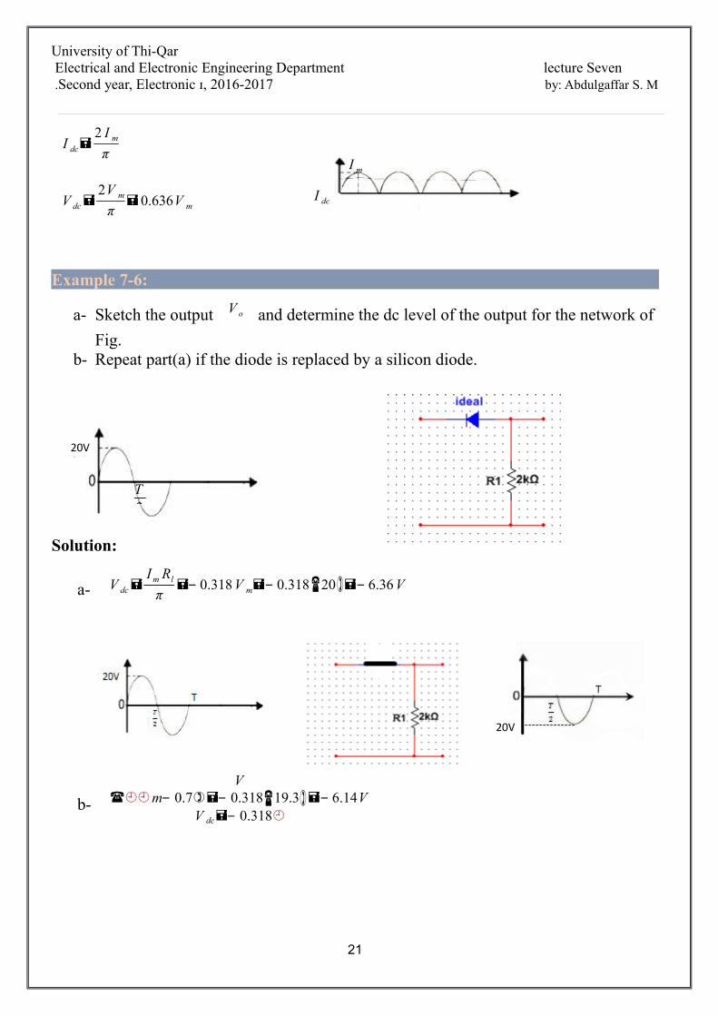
Example 7-6:
a- Sketch the output V o and determine the dc level of the output for the network of
Fig.b- Repeat part(a) if the diode is replaced by a silicon diode.
Solution:
a- V dc=I m Rl
π=− 0.318 V m=− 0.318(20)=− 6.36 V
b-
V(¿¿m− 0.7)=− 0.318(19.3)=− 6.14V
V dc=− 0.318¿
21
I dc
I m
20V
T2
20V
University of Thi-QarElectrical and Electronic Engineering Department lecture Seven Second year, Electronic ɪ, 2016-2017 by: Abdulgaffar S. M.
Example7-7:
For the circuit shown below find V dc & PIV.
Solution:
V P=√ 2V rms=√ 2∗120=170 V
V m=N 1
N 2
V P=14∗170=42.5V
V dc=V m
π=
42.5π
=13.5V
PIV =V m=42.5 V
Example 7-8:
Determine the output waveform for the network of Fig.7- . and calculate the output dc level and the required PIV of each ideal diode.
22
20−0.7=19.3
120V
60Hz
2k
2k
2k
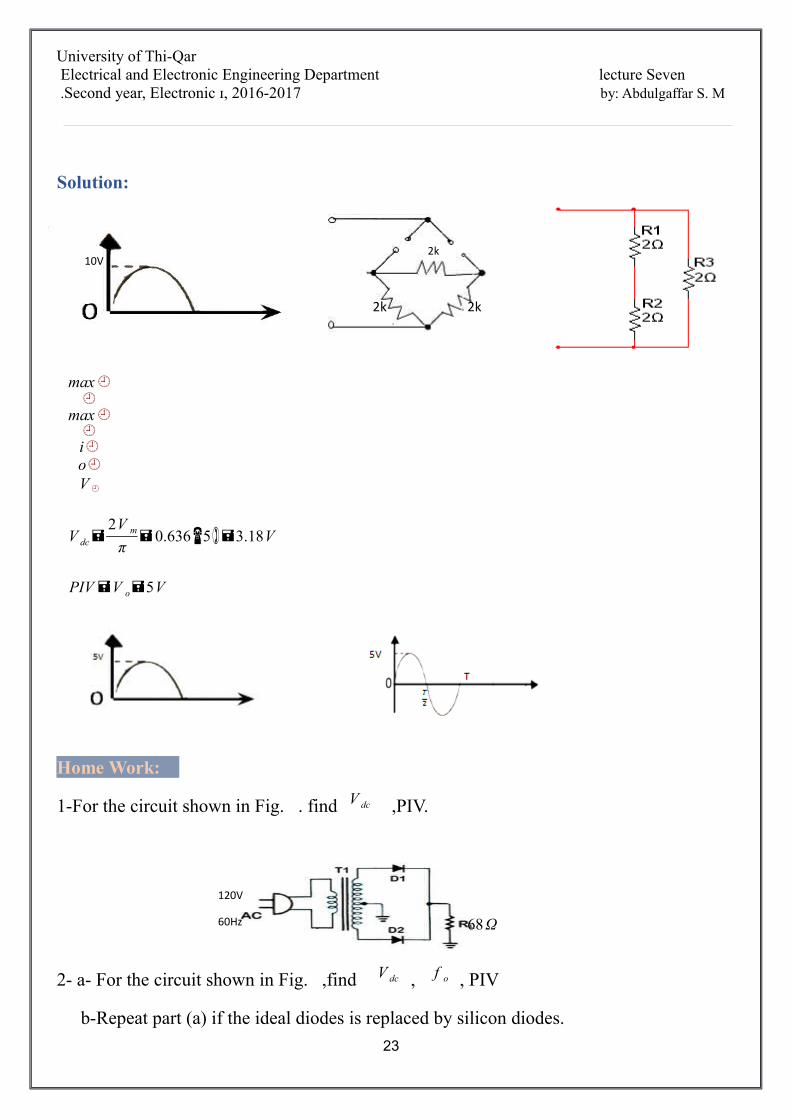
University of Thi-QarElectrical and Electronic Engineering Department lecture Seven Second year, Electronic ɪ, 2016-2017 by: Abdulgaffar S. M.
Solution:
max¿¿
max¿¿i¿o¿V¿
V dc=2V m
π=0.636(5)=3.18V
PIV =V o=5V
Home Work:
1-For the circuit shown in Fig. . find V dc ,PIV.
2- a- For the circuit shown in Fig. ,find V dc , f o , PIV
b-Repeat part (a) if the ideal diodes is replaced by silicon diodes.
23
2k
2k2k
10V
120V
60Hz 68Ω
University of Thi-QarElectrical and Electronic Engineering Department lecture Seven Second year, Electronic ɪ, 2016-2017 by: Abdulgaffar S. M.
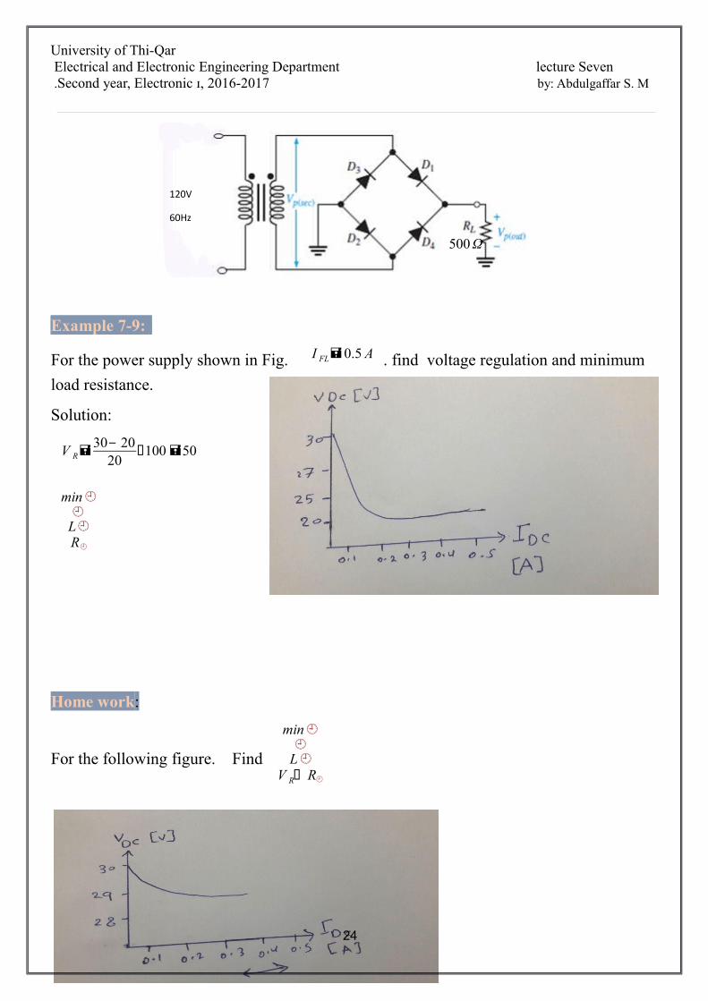
Example 7-9:
For the power supply shown in Fig. I FL=0.5 A . find voltage regulation and minimum
load resistance.
Solution:
V R=30− 20
20∗100 =50
min¿¿
L¿R¿
Home work:
For the following figure. Find
min¿¿
L¿V R∧ R¿
24
120V
60Hz
500 Ω
University of Thi-QarElectrical and Electronic Engineering Department lecture Seven Second year, Electronic ɪ, 2016-2017 by: Abdulgaffar S. M.
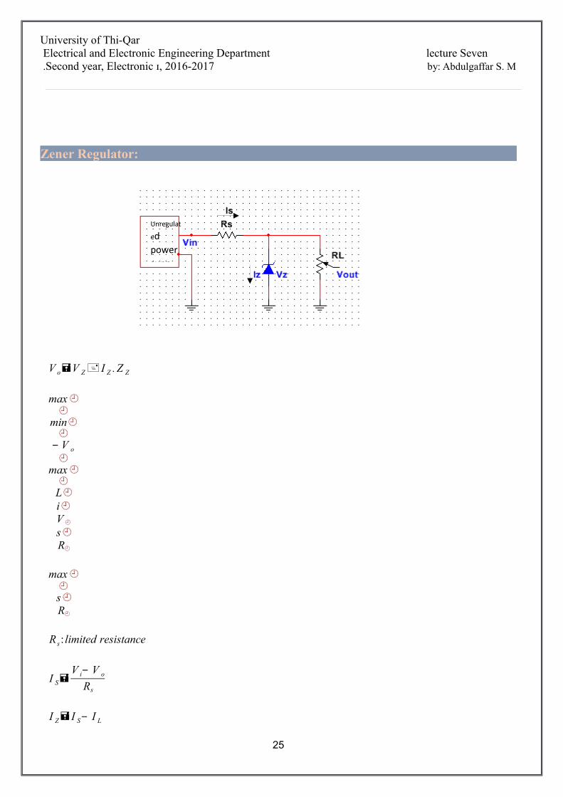
Zener Regulator:
V o=V Z + I Z . Z Z
max¿¿
min¿¿− V o
¿max¿¿
L¿i¿V¿
s¿R¿
max¿¿s¿R¿
R s : limited resistance
I S=V i− V o
Rs
I Z= I S− I L
25
Unregulat
ed power supp
University of Thi-QarElectrical and Electronic Engineering Department lecture Seven Second year, Electronic ɪ, 2016-2017 by: Abdulgaffar S. M.
V o=V Z
I L=V o
Rl
Open CCT.
max¿L¿
I Z=0 , I S= I L= I¿
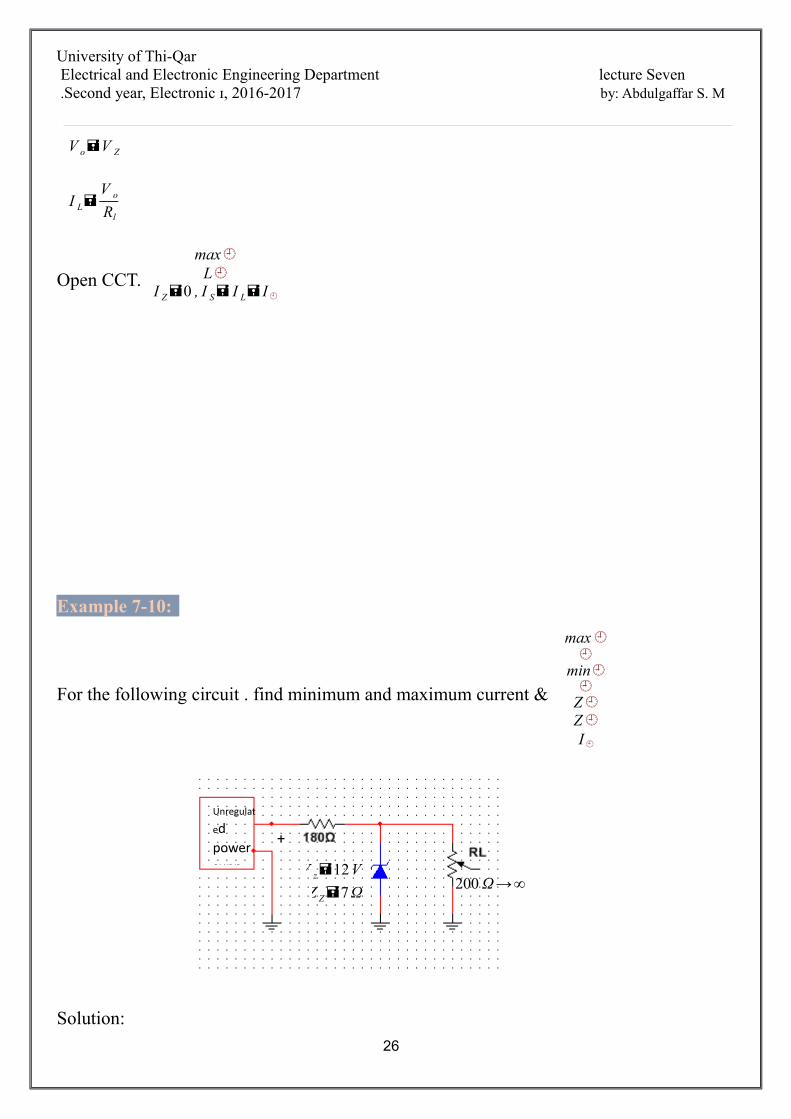
Example 7-10:
For the following circuit . find minimum and maximum current &
max¿¿
min¿¿
Z¿Z¿I¿
Solution:
26
Unregulat
ed power supp
+25
V z=12V200 Ω → ∞
Z Z=7 Ω
University of Thi-QarElectrical and Electronic Engineering Department lecture Seven Second year, Electronic ɪ, 2016-2017 by: Abdulgaffar S. M.
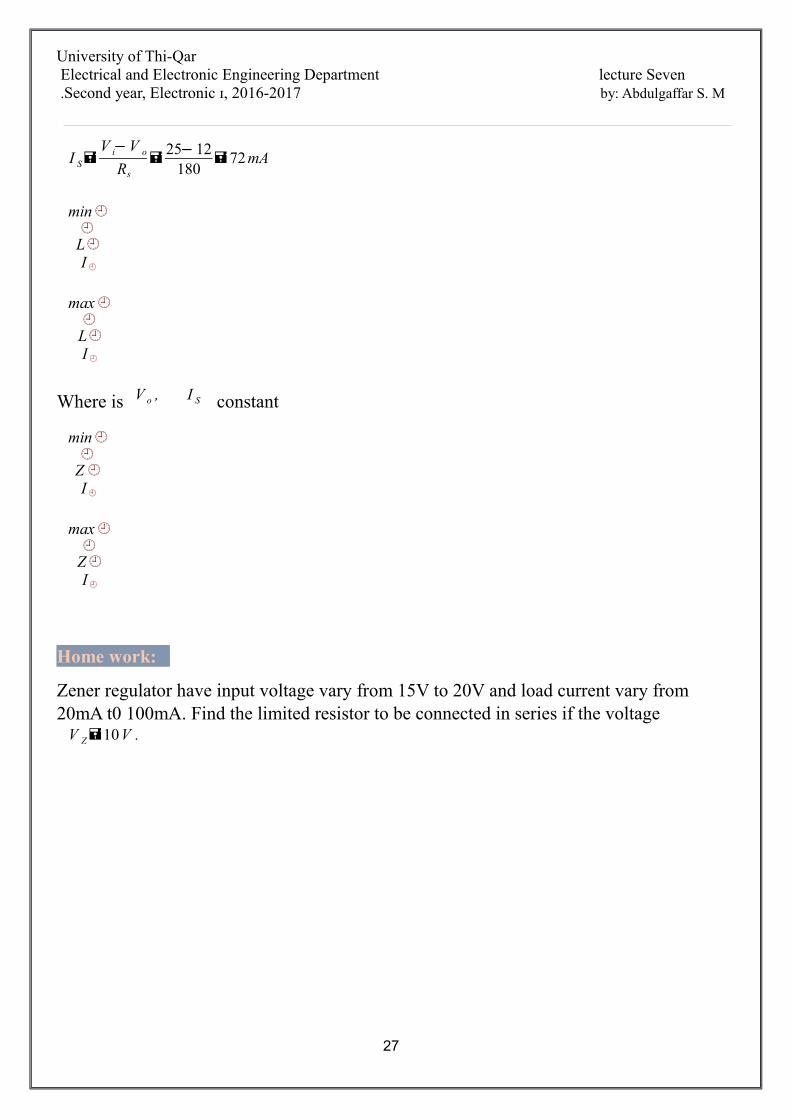
I S=V i− V o
Rs
=25− 12
180=72 mA
min¿¿
L¿I¿
max¿¿L¿I¿
Where is V o , I S constant
min¿¿
Z ¿I¿
max¿¿
Z¿I¿
Home work:
Zener regulator have input voltage vary from 15V to 20V and load current vary from 20mA t0 100mA. Find the limited resistor to be connected in series if the voltage
V Z=10V .
27
University of Thi-QarElectrical and Electronic Engineering Department lecture Seven Second year, Electronic ɪ, 2016-2017 by: Abdulgaffar S. M.
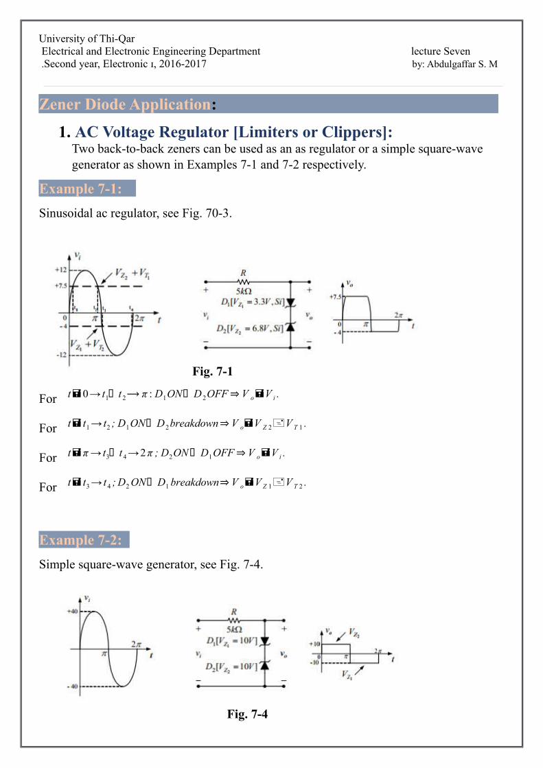
Zener Diode Application:
1. AC Voltage Regulator [Limiters or Clippers]:Two back-to-back zeners can be used as an as regulator or a simple square-wave generator as shown in Examples 7-1 and 7-2 respectively.
Example 7-1:
Sinusoidal ac regulator, see Fig. 70-3.
For t=0→t1∧ t 2⟶ π : D1ON∧ D 2OFF⇒ V o=V i .
For t= t1 →t2 ; D1ON∧ D2breakdown⇒ V o=V Z 2+V T 1 .
For t=π →t3∧ t 4 →2π ; D2ON∧ D1OFF⇒ V o=V i .
For t= t3 →t 4 ; D2 ON∧ D1 breakdown⇒ V o=V Z 1+V T 2 .
Example 7-2:
Simple square-wave generator, see Fig. 7-4.
28
Fig. 7-1
Fig. 7-4
University of Thi-QarElectrical and Electronic Engineering Department lecture Seven Second year, Electronic ɪ, 2016-2017 by: Abdulgaffar S. M.
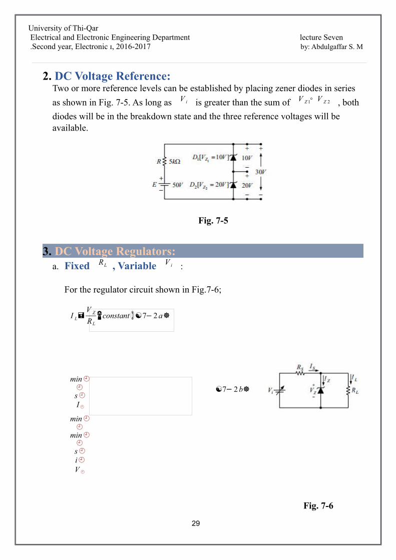
2. DC Voltage Reference:Two or more reference levels can be established by placing zener diodes in series
as shown in Fig. 7-5. As long as V i is greater than the sum of V Z 1∧ V Z 2 , both
diodes will be in the breakdown state and the three reference voltages will be available.
3. DC Voltage Regulators:a. Fixed RL , Variable V i :
For the regulator circuit shown in Fig.7-6;
I L=V Z
RL(constant)[7− 2 a]
min¿¿s¿I¿
min¿¿
min¿¿s¿i¿V ¿
29
Fig. 7-5
[7− 2 b]
Fig. 7-6
University of Thi-QarElectrical and Electronic Engineering Department lecture Seven Second year, Electronic ɪ, 2016-2017 by: Abdulgaffar S. M.
max¿¿s¿I¿
max¿¿
max¿¿s¿i¿V¿
30
[7− 2c]
University of Thi-QarElectrical and Electronic Engineering Department lecture Seven Second year, Electronic ɪ, 2016-2017 by: Abdulgaffar S. M.
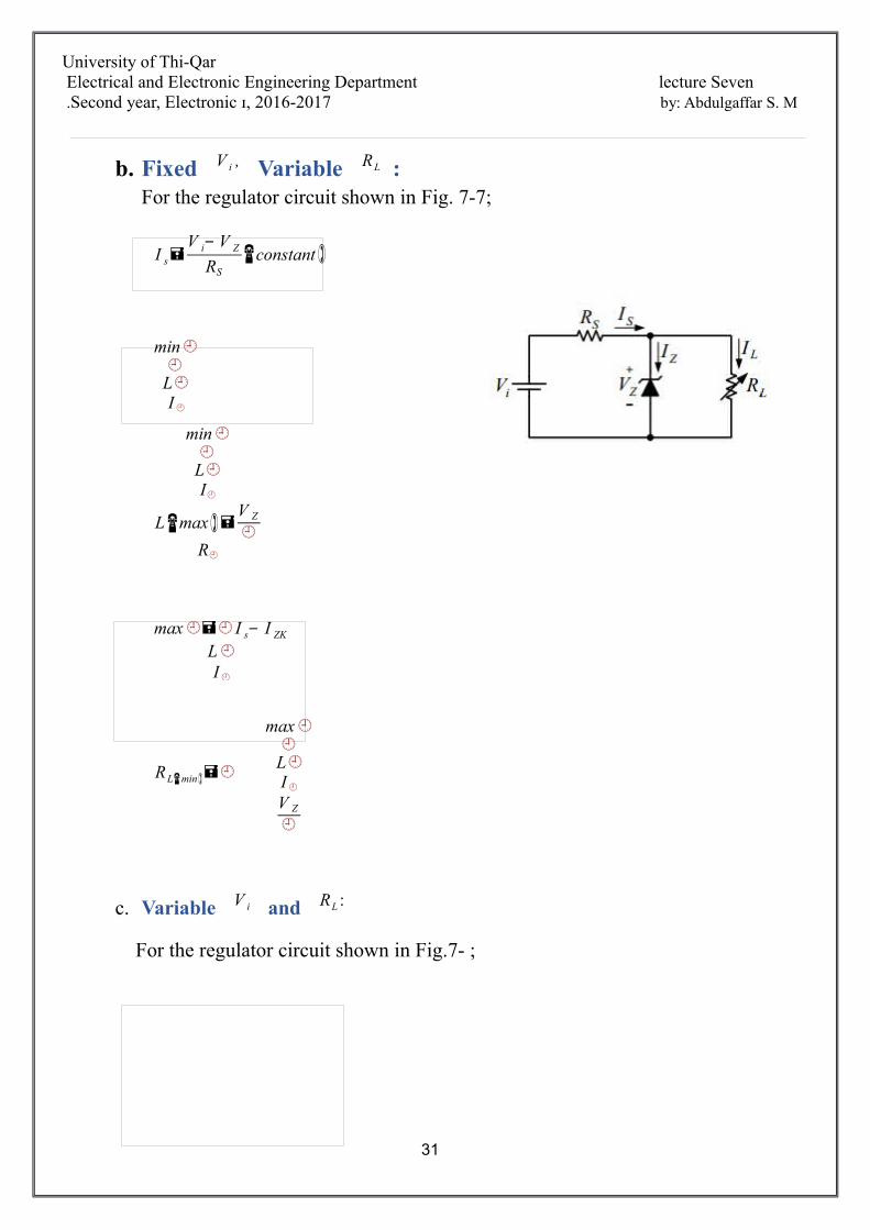
b. Fixed V i , Variable RL :For the regulator circuit shown in Fig. 7-7;
I s=V i− V Z
RS(constant)
min¿¿
L¿I¿
min¿¿L¿I¿
L (max)=V Z
¿R¿
max¿=¿ I s− I ZK
L¿I¿
RL(min)=¿
max¿¿L¿I¿V Z
¿
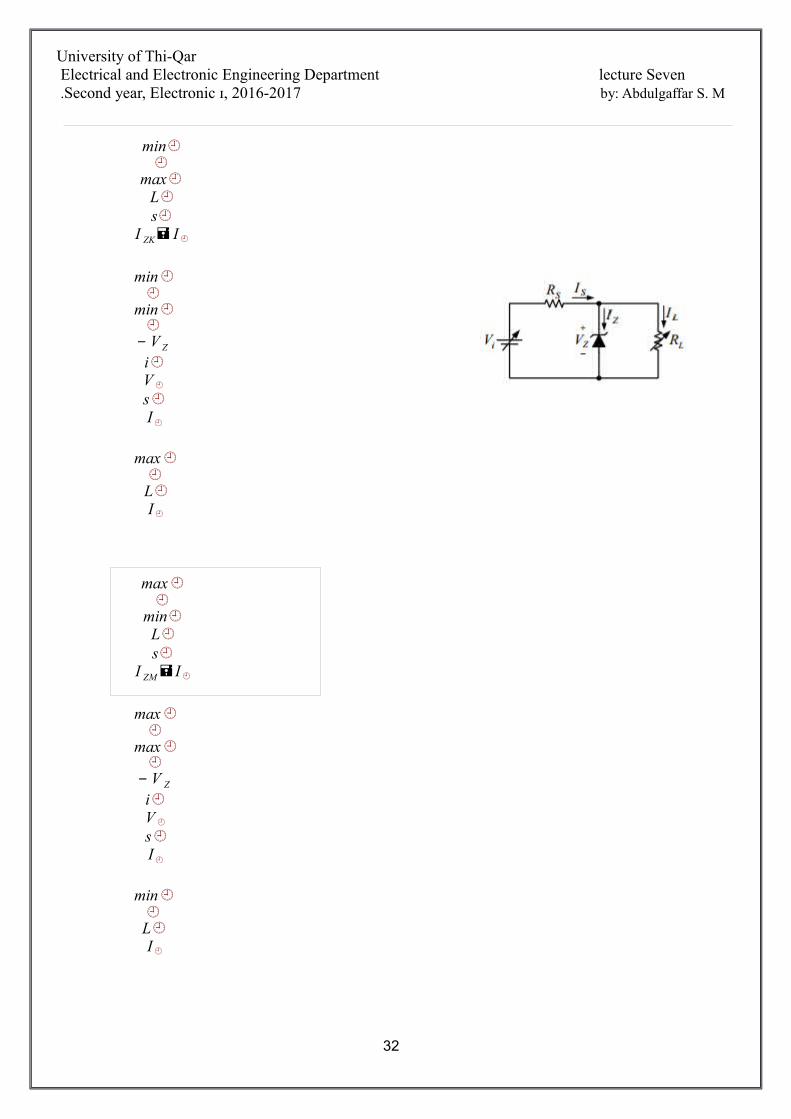
c. Variable V i and RL :
For the regulator circuit shown in Fig.7- ;
31
University of Thi-QarElectrical and Electronic Engineering Department lecture Seven Second year, Electronic ɪ, 2016-2017 by: Abdulgaffar S. M.
min¿¿
max¿L¿s¿
I ZK= I¿
min¿¿
min¿¿− V Z
i¿V¿
s¿I¿
max¿¿L¿I¿
max¿¿
min¿L¿s¿
I ZM = I¿
max¿¿
max¿¿
− V Z
i¿V¿
s¿I¿
min¿¿
L¿I¿
32
University of Thi-QarElectrical and Electronic Engineering Department lecture Seven Second year, Electronic ɪ, 2016-2017 by: Abdulgaffar S. M.
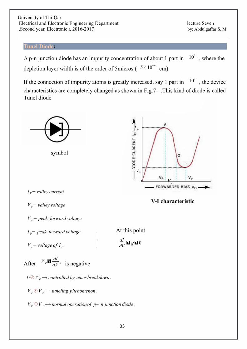
Tunel Diode:
A p-n junction diode has an impurity concentration of about 1 part in 108, where the
depletion layer width is of the order of 5micros ( 5× 10⁻⁴cm).
If the connection of impurity atoms is greatly increased, say 1 part in 103, the device
characteristics are completely changed as shown in Fig.7- .This kind of diode is calledTunel diode
I V−valley current
V V− valley voltage
V F− peak forward voltage
I P− peak forward voltage
V P−voltage of I P
After V P=dIdV
, is negative
0¿V P⟶ controlled by zener breakdown .
V P¿V V⟶ tuneling phenomenon.
V V ¿V P⟶ normal operationof p− n junction diode .
33
At this point
dIdV
=g=0
symbol
I P
I V
V F
V-I characteristic

University of Thi-QarElectrical and Electronic Engineering Department lecture Seven Second year, Electronic ɪ, 2016-2017 by: Abdulgaffar S. M.
34
University of Thi-QarElectrical and Electronic Engineering Department lecture Seven Second year, Electronic ɪ, 2016-2017 by: Abdulgaffar S. M.
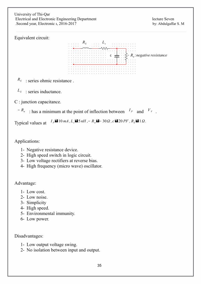
Equivalent circuit:
RS : series ohmic resistance .
LS : series inductance.
C : junction capacitance.
− Rn : has a minimum at the point of inflection between I P and V V .
Typical values at I P=10 mA ,Ls=5nH ,− Rn=− 30Ω ,c=20 PF , RS=1Ω .
Applications:
1- Negative resistance device.2- High speed switch in logic circuit.3- Low voltage rectifiers at reverse bias.4- High frequency (micro wave) oscillator.
Advantage:
1- Low cost.2- Low noise.3- Simplicity 4- High speed.5- Environmental immunity.6- Low power.
Disadvantages:
1- Low output voltage swing.2- No isolation between input and output.
35
RS L s
c − Rn :negative resistance
University of Thi-QarElectrical and Electronic Engineering Department lecture Seven Second year, Electronic ɪ, 2016-2017 by: Abdulgaffar S. M.
Notes:
I P : determined by impurity concentration (the resistivity) & the junction area.
V P , I P−¿ not very temp sensitive.
Tunel diode – excellent conductor in reverse direction.
Ge GaAs siI P/V P 8 15 3.5
V P , V 0.055 0.15 0.065
V V , V 0.35 0.50 0.42
V F ,V 0.50 1.10 0.70
Typical tunel diodes parameter.
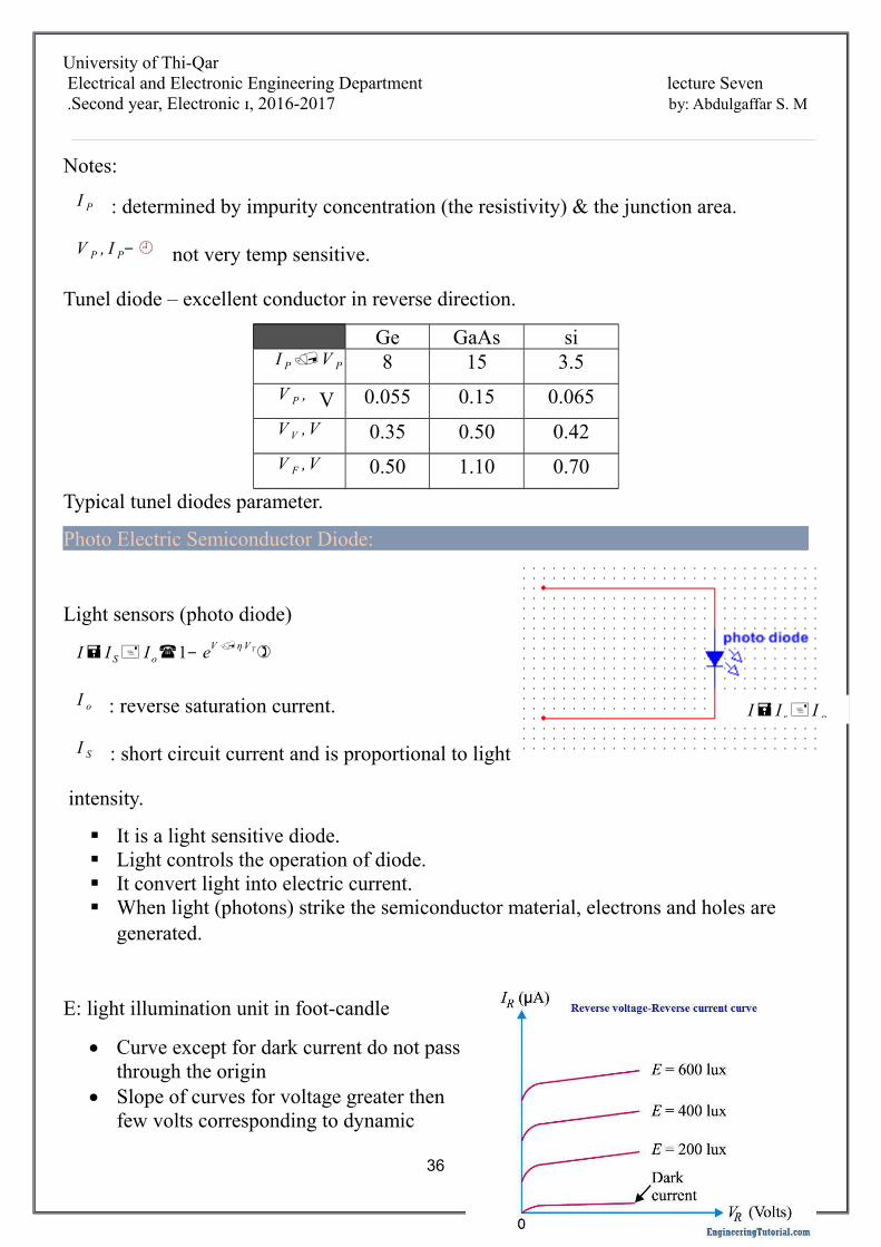
Photo Electric Semiconductor Diode:
Light sensors (photo diode)
I= I S+ I o(1− eV /η V T)
I o : reverse saturation current.
I S : short circuit current and is proportional to light
intensity.
It is a light sensitive diode. Light controls the operation of diode. It convert light into electric current. When light (photons) strike the semiconductor material, electrons and holes are
generated.
E: light illumination unit in foot-candle
Curve except for dark current do not pass through the origin
Slope of curves for voltage greater then few volts corresponding to dynamic
36
I= I s+ I o
University of Thi-QarElectrical and Electronic Engineering Department lecture Seven Second year, Electronic ɪ, 2016-2017 by: Abdulgaffar S. M.
resistance of the order of few μΩ to
hundreds of μΩ .
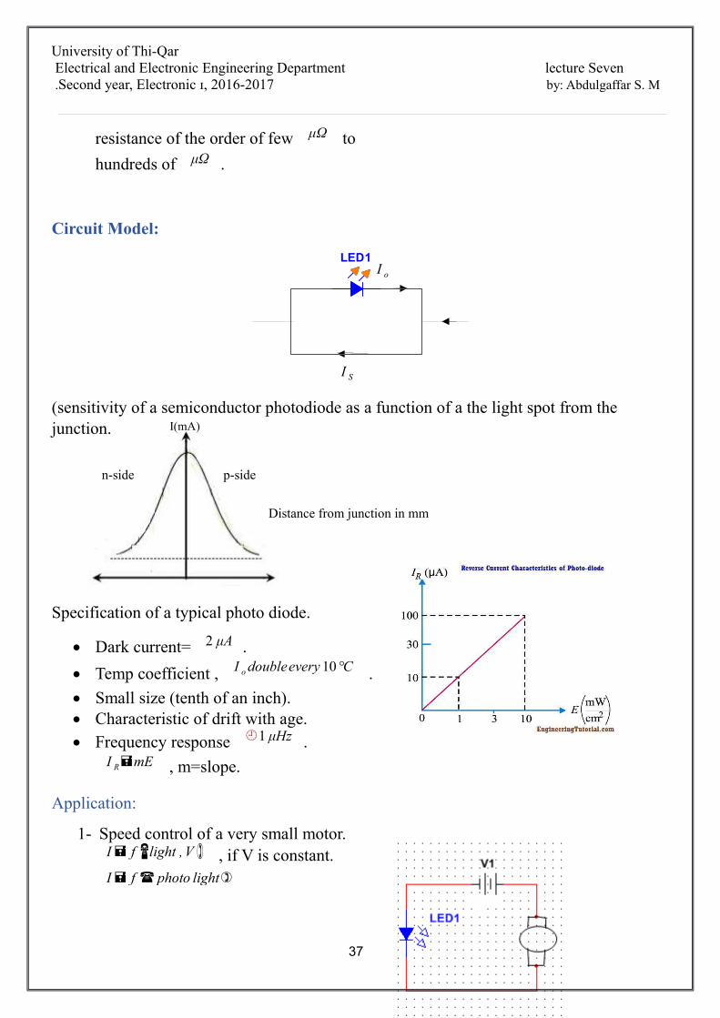
Circuit Model:
LED1
(sensitivity of a semiconductor photodiode as a function of a the light spot from the junction.
Specification of a typical photo diode.
Dark current= 2 μA .
Temp coefficient , I o doubleevery 10 .
Small size (tenth of an inch). Characteristic of drift with age. Frequency response ¿1 μHz .
I R=mE , m=slope.
Application:
1- Speed control of a very small motor.I= f (light ,V ) , if V is constant.I= f ( photo light)
37
I o
I S
I
I(mA)
p-siden-side
Distance from junction in mm
University of Thi-QarElectrical and Electronic Engineering Department lecture Seven Second year, Electronic ɪ, 2016-2017 by: Abdulgaffar S. M.
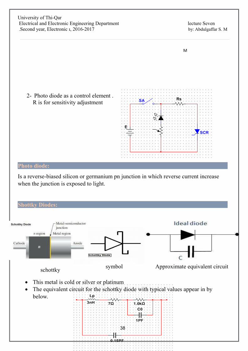
2- Photo diode as a control element .R is for sensitivity adjustment
Photo diode:
Is a reverse-biased silicon or germanium pn junction in which reverse current increase when the junction is exposed to light.
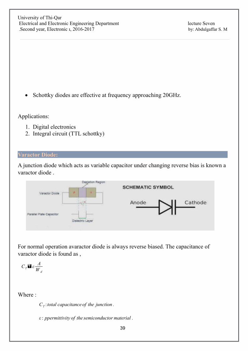
Shottky Diodes:
This metal is cold or silver or platinum The equivalent circuit for the schottky diode with typical values appear in by
below.
38
M
schottkysymbol Approximate equivalent circuit
University of Thi-QarElectrical and Electronic Engineering Department lecture Seven Second year, Electronic ɪ, 2016-2017 by: Abdulgaffar S. M.
Schottky diodes are effective at frequency approaching 20GHz.
Applications:
1. Digital electronics 2. Integral circuit (TTL schottky)
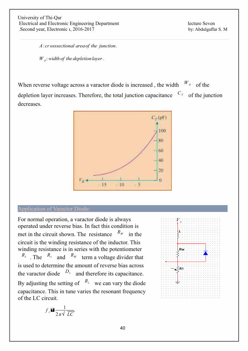
Varactor Diode:
A junction diode which acts as variable capacitor under changing reverse bias is known a varactor diode .
For normal operation avaractor diode is always reverse biased. The capacitance of varactor diode is found as ,
CT=εA
W d
Where :
CT : total capacitance of the junction .
ε : ppermittivity of the semiconductor material .
39
University of Thi-QarElectrical and Electronic Engineering Department lecture Seven Second year, Electronic ɪ, 2016-2017 by: Abdulgaffar S. M.
A :cr osssectional areaof the junction .
W d : width of the depletionlayer .
When reverse voltage across a varactor diode is increased , the width W d of the
depletion layer increases. Therefore, the total junction capacitance CT of the junction
decreases.
Application of Varactor Diode:
For normal operation, a varactor diode is always operated under reverse bias. In fact this condition is
met in the circuit shown. The resistance RW in the
circuit is the winding resistance of the inductor. This winding resistance is in series with the potentiometer
R1 . The R1 and RW term a voltage divider that
is used to determine the amount of reverse bias across
the varactor diode D1 and therefore its capacitance.
By adjusting the setting of R1 we can vary the diode
capacitance. This in tune varies the resonant frequency of the LC circuit.
f r=1
2 π√ LC
40
V s
University of Thi-QarElectrical and Electronic Engineering Department lecture Seven Second year, Electronic ɪ, 2016-2017 by: Abdulgaffar S. M.
If the a mount of varactor reverse bias is decreased. The value of C of the varactor increases. The increases in C will cause the resonant frequency of the circuit to decrease and vice-versa.
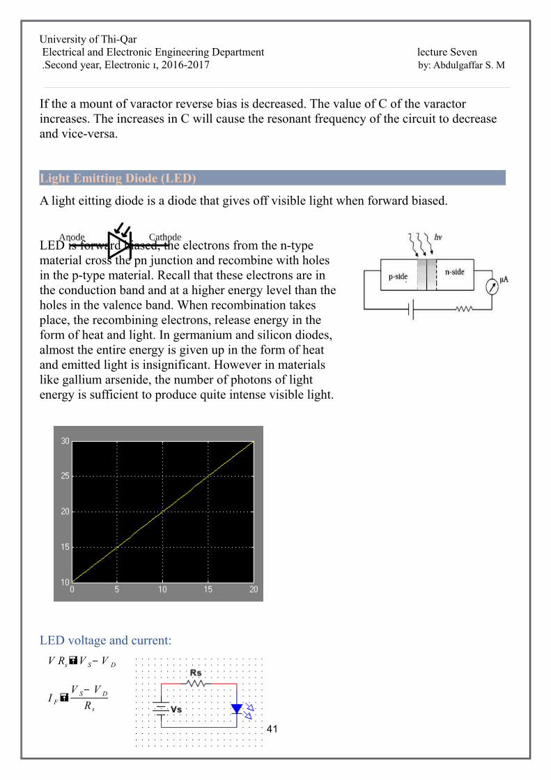
Light Emitting Diode (LED)
A light eitting diode is a diode that gives off visible light when forward biased.
LED is forward biased, the electrons from the n-type material cross the pn junction and recombine with holes in the p-type material. Recall that these electrons are in the conduction band and at a higher energy level than the holes in the valence band. When recombination takes place, the recombining electrons, release energy in the form of heat and light. In germanium and silicon diodes, almost the entire energy is given up in the form of heat and emitted light is insignificant. However in materials like gallium arsenide, the number of photons of light energy is sufficient to produce quite intense visible light.
LED voltage and current:
V Rs=V S− V D
I F=V S− V D
R s
41
University of Thi-QarElectrical and Electronic Engineering Department lecture Seven Second year, Electronic ɪ, 2016-2017 by: Abdulgaffar S. M.
Advantages of LED:
The light emitting diode(LED) is a soild-state light source
1- low voltage2- longer life(more than 20 years)3- fast ON-OFF switching
protecting LED against reverse bias:
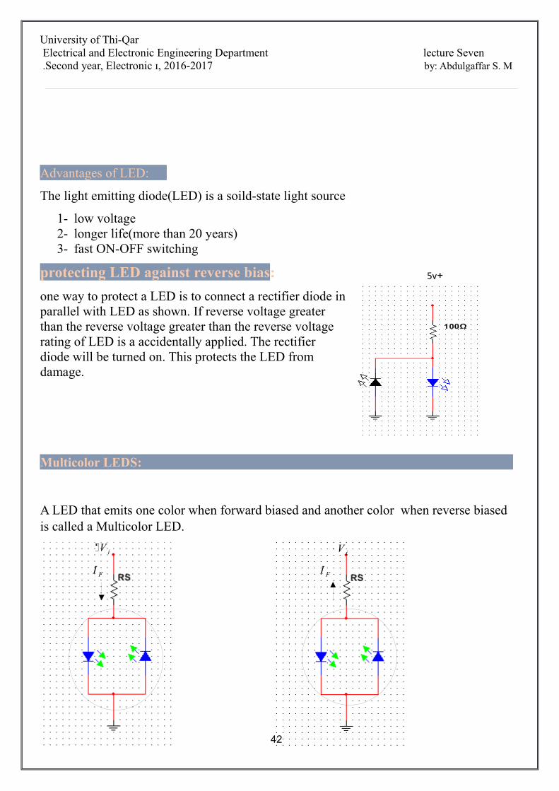
one way to protect a LED is to connect a rectifier diode inparallel with LED as shown. If reverse voltage greater than the reverse voltage greater than the reverse voltage rating of LED is a accidentally applied. The rectifier diode will be turned on. This protects the LED from damage.
Multicolor LEDS:
A LED that emits one color when forward biased and another color when reverse biased is called a Multicolor LED.
42
+V i
I F
− V i
I F
+5v
University of Thi-QarElectrical and Electronic Engineering Department lecture Seven Second year, Electronic ɪ, 2016-2017 by: Abdulgaffar S. M.
Multicolor LEDs are typically red when biased in one direction and green when biased inthe other. If a multicolor LED is switched fast enough between two polarities, the LED will produce a third color. A red\ green will produce yellow.
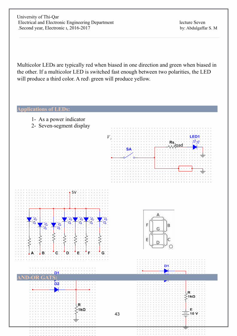
Applications of LEDs:
1- As a power indicator2- Seven-segment display
AND-OR GATS:
43
load
V i
5V
University of Thi-QarElectrical and Electronic Engineering Department lecture Seven Second year, Electronic ɪ, 2016-2017 by: Abdulgaffar S. M.
Shockley diode:
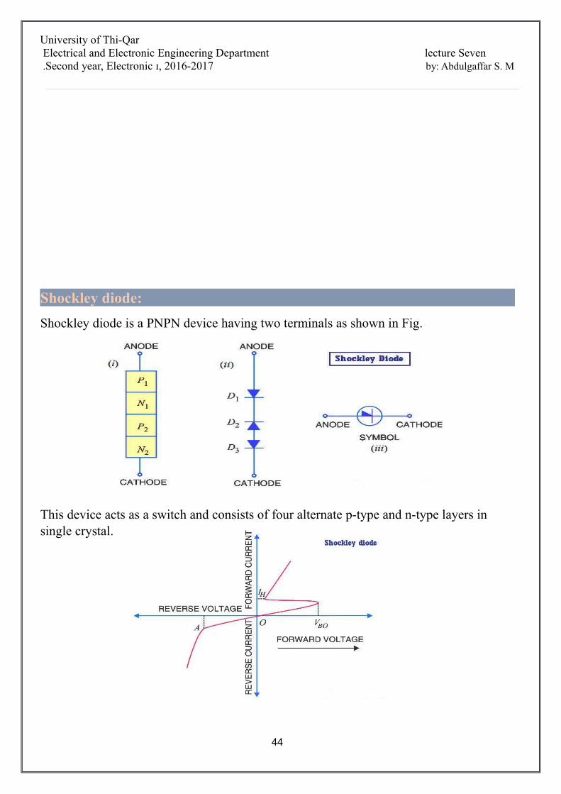
Shockley diode is a PNPN device having two terminals as shown in Fig.
This device acts as a switch and consists of four alternate p-type and n-type layers in single crystal.
44
University of Thi-QarElectrical and Electronic Engineering Department lecture Seven Second year, Electronic ɪ, 2016-2017 by: Abdulgaffar S. M.
Forward D1∧ D3 but D2 reverse biased to V =V B0 then D2 in reverse
breakdown. From now onwards. The shockly diode behaves as a conventional forward
biased diode. At reverse D1∧ D3 in reverse & D2 forward to point A breakdownD1∧ D3 .
45
University of Thi-QarElectrical and Electronic Engineering Department lecture Seven Second year, Electronic ɪ, 2016-2017 by: Abdulgaffar S. M.
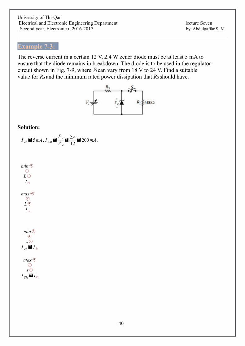
Example 7-3:
The reverse current in a certain 12 V, 2.4 W zener diode must be at least 5 mA toensure that the diode remains in breakdown. The diode is to be used in the regulatorcircuit shown in Fig. 7-9, where Vi can vary from 18 V to 24 V. Find a suitablevalue for RS and the minimum rated power dissipation that RS should have.
Solution:
I ZK=5 mA, I ZM =PZ
V Z
=2.412
=200 mA.
min¿¿
L¿I¿
max¿¿
L¿I¿
min¿¿s¿
I ZK= I¿
max¿¿s¿
I ZM= I¿
46
University of Thi-QarElectrical and Electronic Engineering Department lecture Seven Second year, Electronic ɪ, 2016-2017 by: Abdulgaffar S. M.
min¿¿
− V Z
¿min¿¿s¿i¿V ¿
R s(max)=¿
max¿¿
− V Z
¿max¿¿s¿i¿V ¿
R s(min)=¿
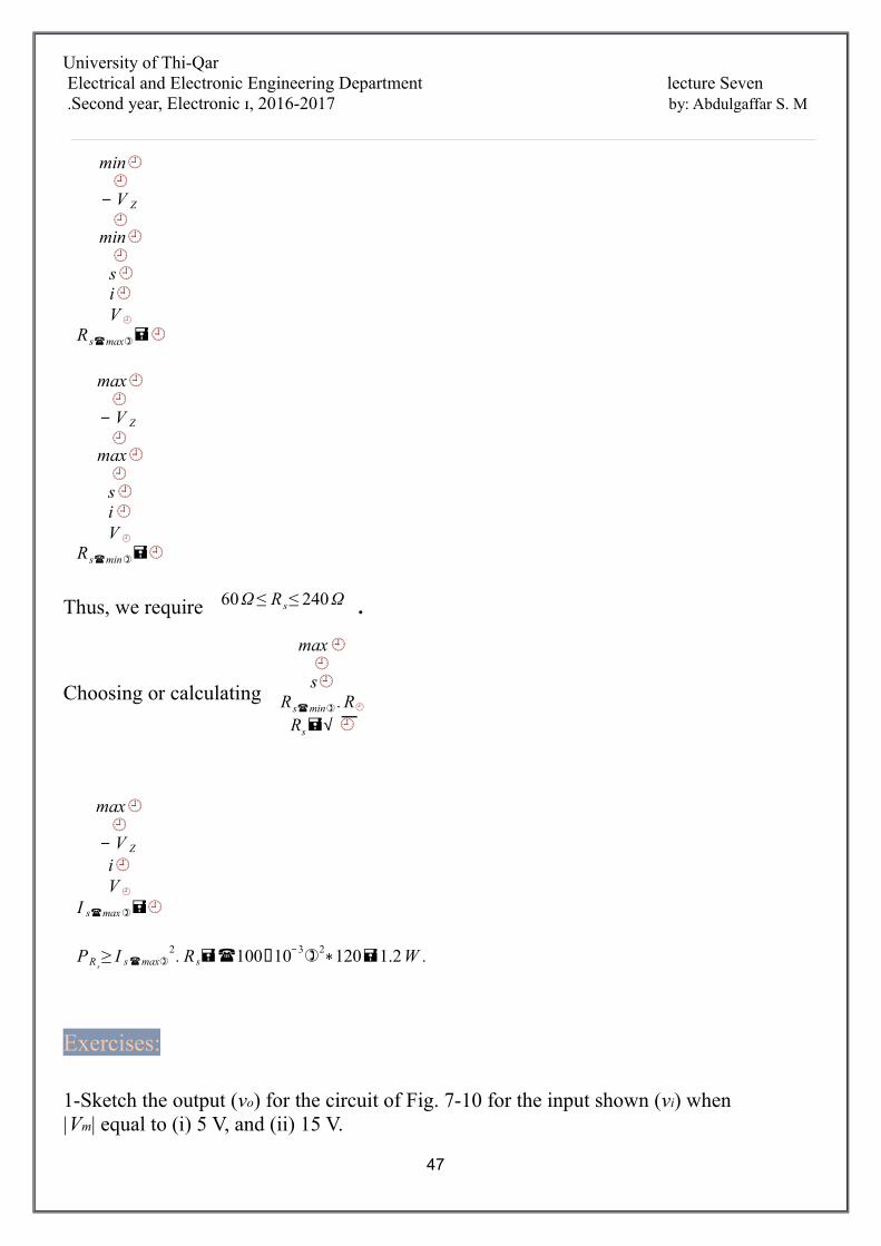
Thus, we require 60Ω ≤ R s≤ 240 Ω .
Choosing or calculating
max¿¿s¿
R s(min) .R¿
Rs=√ ¿
max¿¿
− V Z
i¿V ¿
I s(max)=¿
PR s≥ I s(max)
2. R s=(100∗10−3)2∗120=1.2W .
Exercises:
1-Sketch the output (vo) for the circuit of Fig. 7-10 for the input shown (vi) when|Vm| equal to (i) 5 V, and (ii) 15 V.
47
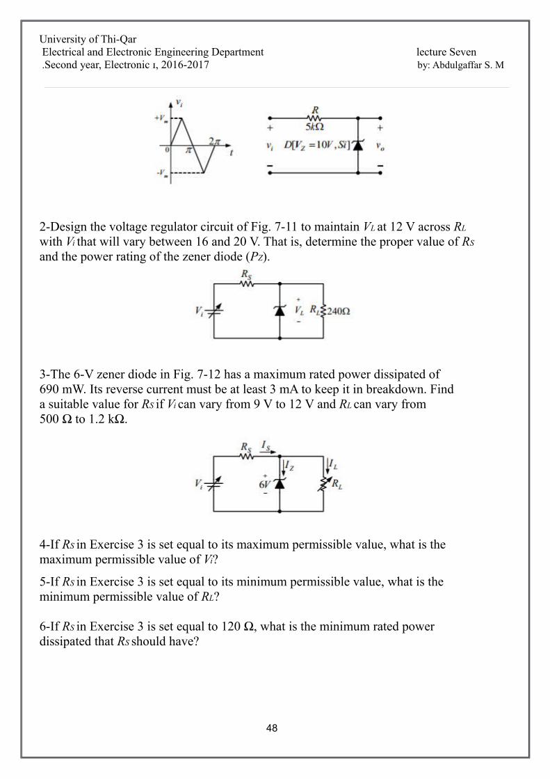
University of Thi-QarElectrical and Electronic Engineering Department lecture Seven Second year, Electronic ɪ, 2016-2017 by: Abdulgaffar S. M.
2-Design the voltage regulator circuit of Fig. 7-11 to maintain VL at 12 V across RL
with Vi that will vary between 16 and 20 V. That is, determine the proper value of RS
and the power rating of the zener diode (PZ).
3-The 6-V zener diode in Fig. 7-12 has a maximum rated power dissipated of690 mW. Its reverse current must be at least 3 mA to keep it in breakdown. Finda suitable value for RS if Vi can vary from 9 V to 12 V and RL can vary from500 Ω to 1.2 kΩ.
4-If RS in Exercise 3 is set equal to its maximum permissible value, what is themaximum permissible value of Vi?
5-If RS in Exercise 3 is set equal to its minimum permissible value, what is theminimum permissible value of RL?
6-If RS in Exercise 3 is set equal to 120 Ω, what is the minimum rated powerdissipated that RS should have?
48
University of Thi-QarElectrical and Electronic Engineering Department lecture Seven Second year, Electronic ɪ, 2016-2017 by: Abdulgaffar S. M.
49