zigzag slabs for solid-state laser amplifiers: batch ...rlbyer/pdf_allpubs/2006/421.pdf · zigzag...
TRANSCRIPT
Zigzag slabs for solid-state laser amplifiers: batchfabrication and parasitic oscillation suppression
Arun Kumar Sridharan, Shailendhar Saraf, Supriyo Sinha, and Robert L. Byer
We have developed a 100 W class Nd:YAG master oscillator power amplifier system based in part on anend-pumped zigzag slab power amplifier. This amplifier incorporates parasitic oscillation suppression byusing roughened edges and achieves a small-signal gain coefficient �g0l� of 8.06. We describe a noveltechnique for suppression of parasitic oscillations using claddings on slab edges that significantly in-creases g0l to 11.63 and increases the single-pass extracted power in a power amplifier by 50%. Com-mercial use of these zigzag slab amplifiers has been limited by the time and cost of production. Wedescribe a new batch fabrication technique that improves the quality and significantly reduces the costof zigzag slabs. © 2006 Optical Society of America
OCIS codes: 140.3280, 140.3350.
1. Introduction
Applications such as gravitational-wave detectionrequire high-average-power laser sources with ahigh degree of spectral and spatial coherence. Forexample, the proposed Advanced Laser Inter-ferometer Gravitational Wave Observatory (LIGO)requires a 200 W, single-longitudinal-mode, single-transverse-mode Nd:YAG laser as compared with the10 W laser used continually on site since 1997.1,2 Sev-eral approaches to meet this requirement are beinginvestigated. Traditional rod-based injection-lockedlasers operate at 114 W.3 Thermal lensing and stress-induced birefringence present challenges to theirpower scaling. Large-core double-clad fiber amplifier-based sources have reached 264 W of output power.4However, their phase noise, pointing stability, andlong-term reliability have to be characterized withrespect to the demanding LIGO requirements. Wehave investigated a master oscillator power amplifier(MOPA) approach based on end-pumped zigzag slabamplifiers to take advantage of the well-knownpower scaling of slab lasers and the reliability andcoherence-preserving properties of power amplifica-tion.
In addition to scientific applications, commercialapplications also motivate several approaches forscaling solid-state lasers to high average powers.For example, active mirror slab lasers also knownas thin-disk lasers, first invented by Martin andChernoch5 and extensively developed by Giesen andcolleagues,6,7 have reached the 1 kW class in multi-ple transverse modes. Power scaling is difficult be-cause of their one-sided cooling and the practicalaspects to operate at a thickness below 100 �m. Thezigzag, rectilinear geometry, slab-based5 MOPA sys-tem can scale to higher average powers while main-taining a high beam quality. The slab lasers arecooled symmetrically on both sides and their averagepower output scales with the cooled area. The nearlyone-dimensional thermal gradients and the zigzagoptical path of slab laser gain media significantlyreduce thermal lensing and stress-induced birefrin-gence compared with traditional rod-based designs.8,9
Early zigzag slab laser designs had low efficienciesdue to flashlamp pumping. Residual phase distor-tions and a complex direct water-cooled laser headadded to the engineering challenges.10 Most of theseengineering problems have now been solved by laserdiode pumping through the end11 and edge12 ofconduction-cooled zigzag slabs.13 Nd:YAG zigzag slablasers now operate at multikilowatt output powerswith good beam quality.14
Motivated by LIGO, we have developed a Nd:YAGlaser in a MOPA configuration. By incorporating theinnovations of conduction cooling, edge pumping, andend pumping we have developed a 104 W single-frequency, single-mode, single-polarization Nd:YAG
The authors are with the Edward L. Ginzton Laboratory,Stanford University, Stanford, California 94305. A. K. Sridharan’se-mail address is [email protected].
Received 30 September 2005; accepted 30 October 2005; posted21 December 2005 (Doc. ID 65087).
0003-6935/06/143340-12$15.00/0© 2006 Optical Society of America
3340 APPLIED OPTICS � Vol. 45, No. 14 � 10 May 2006
MOPA at 1064 nm using four stages of amplifica-tion.15 An end-pumped zigzag slab power amplifierforms the final stage and accepts a 30 W input signalbeam. It is double passed and operates at 104 W withan M2 of 1.08 and 1.13 in the zigzag and nonzigzagdirections, respectively. To determine the spatial co-herence of this system, the MOPA output is modematched into a Fabry–Perot ring resonator called amode cleaner,16 which resonates the TEM00 Gaussianmode. We determined that 89% of the 104 W outputsignal is in the fundamental TEM00 spatial mode, andits degree of polarization is greater than 97%. Theseresults along with quantum noise measurements inan end-pumped, saturated, zigzag Nd:YAG slab am-plifier17 are key milestones in the development of a200 W laser system for the next-generation AdvancedLIGO system.
In this paper we focus on the design, fabrication,and performance of the end-pumped zigzag slabpower amplifier. To achieve power scaling in theMOPA configuration, the power amplifier must bedesigned to allow efficient power extraction. The out-put intensity of a solid-state power amplifier is givenby18
Iout � Iin exp�g0l�1 �Iin
Isat��1�, (1)
where Iout is the output intensity, Iin is the inputsignal intensity, g0 is the small-signal gain coeffi-cient, l is the signal optical path length, and Isat is thesaturation intensity of the gain medium. A high g0land Iin � 2Isat is needed to extract �97% of the avail-able power from a power amplifier. In practice, eitherparasitic oscillations or amplified spontaneous emis-sion (ASE) clamps g0l and thereby limits the extrac-tion efficiency. We present a novel technique thatinvolves application of claddings on the zigzag slab’snon-total-internal-reflection surfaces (edges) to in-crease the parasitic-limited g0l and extracted powerin a saturated amplifier.
Model calculations show that g0l � 7 and a cross-sectional area of 1 mm2 per slab is required to extract170 W of power and achieve 200 W output with anavailable 30 W of input power in two end-pumpedzigzag slab amplifier stages. To achieve efficientpower extraction from the amplifier in a TEM00Gaussian mode, we chose an approximately 1:1�width:thickness � 1.1:0.9 mm� aspect ratio slab.
Fabrication of a high length-to-thickness aspect ra-tio, slab �1.1 mm � 0.9 mm � 66 mm, doped regionwith undoped end caps) presents challenges. Slabsfabricated individually are of lower quality (surfaceflatness and coating properties are not uniform) andhigher cost (ten times higher) than slabs made by thebatch fabrication process presented in this paper. Bynecessity, we developed a cost-effective way for mak-ing zigzag slabs that involves fabricating multipleslabs in batch processing steps. This technique alsoenables production of higher-quality slabs for opti-mum amplifier performance. A key side benefit of this
invention is that it provides a multiplicity of slabs fortesting various parasitic oscillation suppression tech-niques for improved amplifier power extraction.
2. Theory, Design, and Modeling
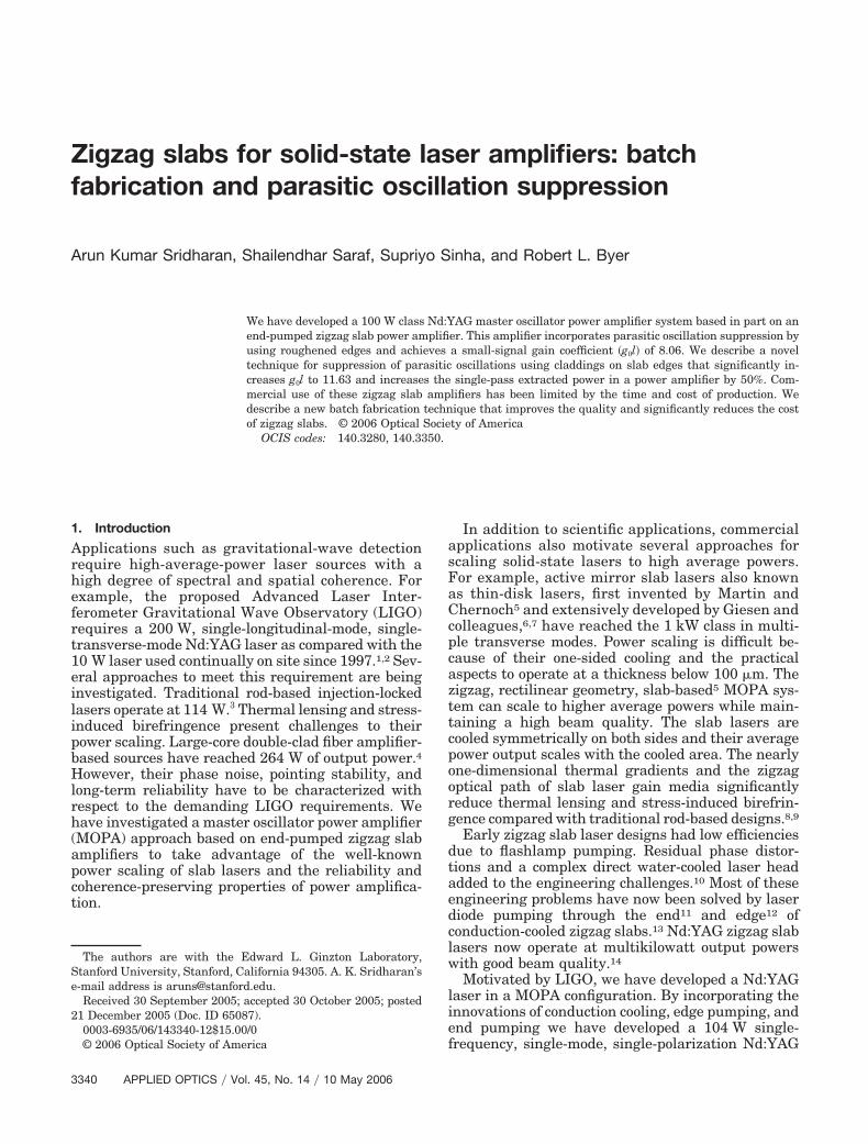
Figure 1 shows a diagram of the end-pumped Nd:YAG zigzag slab amplifier. The amplifier slab ispumped by fiber-coupled laser diodes and reimagedwith a lens into the end of the slab. The slab consistsof a doped region diffusion bonded to undoped endcaps. The pump light undergoes total internal reflec-tion (TIR) at the slanted undoped endface of the slab,is confined by TIR reflections on the four surfaces ofthe undoped end caps, and is absorbed along thelength of the doped region. The length of the dopedregion is designed to avoid stress fracture and max-imize pump absorption, amplifier gain coefficient�g0l�, and power extraction. The signal light is inci-dent at a near-normal angle to the endface and isconfined in the slab via TIR reflections on the top andbottom (side) faces.
A. Theory
First we describe the analytical expressions that gov-ern the performance of the slab amplifier. Zigzag slablaser design was treated earlier by Eggleston et al.8and recently by Chen et al.19,20 Eggleston et al.21 alsoextended Franz and Nodvik’s amplifier anal-ysis22 to zigzag slabs that had regions with and with-out standing waves.
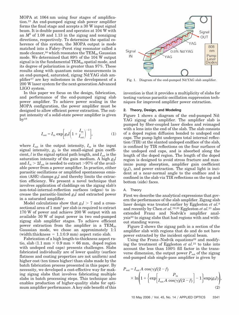
Figure 2 shows the zigzag path in a section of theamplifier slab with regions that do and do not havepower extracted by the incident optical beam.
Using the Franz–Nodvik equations22 and modify-ing the treatment of Eggleston et al.21 to take intoaccount the less than 100% fill factor in the trans-verse dimension, the output power Pout of the zigzagend-pumped slab single-pass amplifier is given by
Pout � Isat A cos���f�2 � f�
� ln(1 ��exp� Pin
Isat A cos���f�2 � f��� 1exp�g0l�),
(2)
Fig. 1. Diagram of the end-pumped Nd:YAG slab amplifier.
10 May 2006 � Vol. 45, No. 14 � APPLIED OPTICS 3341
where Pin is the input signal power and A is the activecross-sectional area of the zigzag slab that is probedby the incident beam and is equal to 2wTHt, where wTHis the top-hat equivalent of the TEM00 Gaussianbeam 1�e2 radius wg in the slab as defined by18
wTH � wg�2. (3)
Here t is the slab thickness and � is the complemen-tary angle to the angle of incidence at the YAG�SiO2interface. The overlap factor f for near-normal inci-dence in a zigzag slab can be calculated by trigonom-etry and is given as
f �Ls
Lb�
1
2
wg
t sec �, (4)
where Ls is the overlap length given by
Ls � 2wg
sin �, (5)
and Lb is the bounce length given by
Lb �2t
tan �. (6)
The small-signal gain coefficient g0l is given by
g0l �Ppump�
wtIsat cos �, (7)
where Ppump is the incident pump power and � is apump efficiency factor given by
� � �abs�p�q. (8)
Here the pump absorption efficiency �abs is given as
�abs � �1 � exp��ldoped���c, (9)
where �c is the confinement efficiency of the pumplight in the slab, � 1.8 cm�1 is the pump absorptioncoefficient for 0.6% Nd:YAG at 808 nm, and ldoped isthe length of the slab’s doped region. �p � 0.92 isthe approximate pump quantum efficiency for 0.6%Nd:YAG,23 and �q � 0.76 is the quantum defect givenby the ratio of signal and pump photon energies.
To model the power extraction from a power am-plifier, the available power in the active cross sectionof this slab power amplifier is given by
Pavail � Ppump�Awt . (10)
The maximum extractable power Pextr for a zigzagoptical path is given as21
Pextr � Pavail f�2 � f�. (11)
The unextracted power Punextracted in the active areadue to the zigzag optical path is given by21
Punextracted � Pavail�1 � f�2. (12)
B. Design
Using these relations, we design the slab amplifier toachieve 100 W of output power with 30 W of inputpower and 430 W of pump power. The signal beammust enter and exit the slab without degradation inbeam quality due to diffraction losses at the endfaces.The length of the doped region is chosen to achievefull absorption of the pump radiation and a suffi-ciently cooled area to avoid stress fracture. The un-doped crystal length must be long enough to preventclipping of the pump radiation as it is focused ontothe slab’s endfaces, adjacent to the copper microchan-nel coolers.
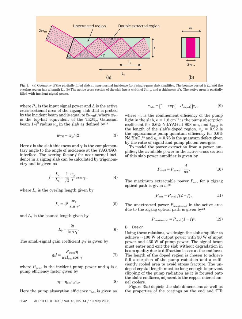
Figure 3(a) depicts the slab dimensions as well asthe properties of the coatings on the end and TIR
Fig. 2. (a) Geometry of the partially filled slab at near-normal incidence for a single-pass slab amplifier. The bounce period is Lb and theoverlap region has a length Ls. (b) The active cross section of the slab has a width of 2wTH and a thickness of t. The active area is partiallyfilled with incident signal power.
3342 APPLIED OPTICS � Vol. 45, No. 14 � 10 May 2006
surfaces. The required slab cross-sectional area is1 mm2. To achieve efficient power extraction from theamplifier in a TEM00 Gaussian mode, we choose anapproximately 1:1 �w:t � 1.1:0.9 mm� aspect ratioslab.
The slab is conduction cooled on the top and bottomfaces. A 3 �m thick SiO2 coating deposited on thesesurfaces ensures TIR zigzag reflections for the signalbeam with minimum loss by allowing the evanescentwave to be attenuated. The net loss for the signalbeam due to residual scattering at the YAG�SiO2interface is less than 0.1%�bounce. A thin indiumfilm thermal layer followed by copper microchannelcoolers24 is placed in contact with the SiO2 layer toextract the heat deposited under operating conditionsin the slab.
In our implementation, the 3 �m thick SiO2 coat-ings provide improved optical performance in two dis-tinct and independent ways. The first function is toachieve an antireflection (AR) coating for light at thepump wavelength p at � � 30° (� is defined as theangle with respect to the normal vector for each sur-face). This coating design reduces losses when opticalend pumping is performed through the TIR surfacesas shown in Fig. 1. The second function is to suppressparasitic oscillations by increasing the loss for spon-taneous emission or ASE rays that are incident on theTIR surfaces at less than the critical angle ��crit�. Thisis achieved by embedding an AR coating at the laserwavelength s within the SiO2 layer. This coating has
a power reflectivity R less than 1% for rays that areincident on the TIR surfaces from within the slab atangles less than 0.9 �crit. �crit for a YAG�SiO2 inter-face is 52.8°, whereas for a YAG�air interface it is33.2°. The coating allows more ASE rays to refractout of the slab and into the SiO2 coating layer andeventually be absorbed in the indium thermal layeror copper microchannel cooler that is in contact withthis coating layer.
An AR coating is also deposited on each of theend-coupling faces of the slab. This coating is a mul-tilayer AR coating at p and s. The coating enablesan alternative for efficient pumping of slabs via theend-coupling faces and ensures minimal loss to theamplified signal beam, respectively. The edge facesare polished at the end of fabrication.
Fabricating a high length-to-width aspect ratioNd:YAG slabs individually is difficult. Slabs madeindividually are of lower quality with respect to sur-face flatness and nonuniform coating properties. Wetherefore developed a mass fabrication techniquethat produced multiple slabs but involved intermedi-ate polishing and coating steps that utilized largesurface areas. The steps include bonding undopedYAG to either side of a doped YAG block to form asandwich, and dicing the sandwich to provide slices.Two of the surfaces of each slice are cut, ground, andpolished as TIR surfaces. The slices’ end surfaces andthe TIR surfaces are appropriately coated. Finally,the coated slice is diced perpendicular to the TIR
Fig. 3. (Color online) (a) Two-dimensional view of the slab with dimensions and coating properties. (b) Photograph of a fabricated Nd:YAGslab.
10 May 2006 � Vol. 45, No. 14 � APPLIED OPTICS 3343
surfaces and the edges are polished to provide manyzigzag slabs at reduced cost. Appendix A describes indetail how the slab described above [Fig. 3(b)] is fab-ricated and the related cost-benefit analysis.
C. Modeling
Using Eqs. (2)–(8), we model the expected perfor-mance of the Nd:YAG end-pumped zigzag slab am-plifier. The initial goal is to achieve �100 W of outputsignal power with 430 W of available pump powerand 30 W of input signal power.
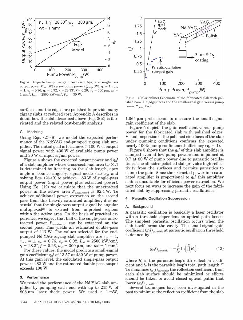
Figure 4 shows the expected output power and g0lof a slab amplifier whose cross-sectional area (w � t)is determined by iterating on the slab length, apexangle �, bounce angle �, signal mode size wg, andsolving Eqs. (2)–(9) to achieve 83 W of single-passoutput power (input power plus extracted power).Using Eq. (12) we calculate that the unextractedpower in the active area Punextracted is 62.4 W. Toachieve additional power extraction on the secondpass from this heavily saturated amplifier, it is es-sential that the single-pass output signal be angularmultiplexed25 to extract from unprobed regionswithin the active area. On the basis of practical ex-perience, we expect that half of the single-pass unex-tracted power Punextracted can be extracted on thesecond pass. This yields an estimated double-passoutput of 117 W. The values selected for the end-pumped Nd:YAG zigzag slab amplifier are �c � 1,�abs � 1, �q � 0.76, �p � 0.92, Isat � 2500 kW�cm2,� � 28.3°, f � 0.26, wg � 300 �m, and wt � 1 mm2.
For these values, the model predicts a small-signalgain coefficient g0l of 13.57 at 430 W of pump power.At this gain level, the calculated single-pass outputpower is 83 W and the estimated double-pass outputexceeds 100 W.
3. Performance
We tested the performance of the Nd:YAG slab am-plifier by pumping each end with up to 215 W of808 nm laser diode power. We used a 1 mW,
1.064 �m probe beam to measure the small-signalgain coefficient of the slab.
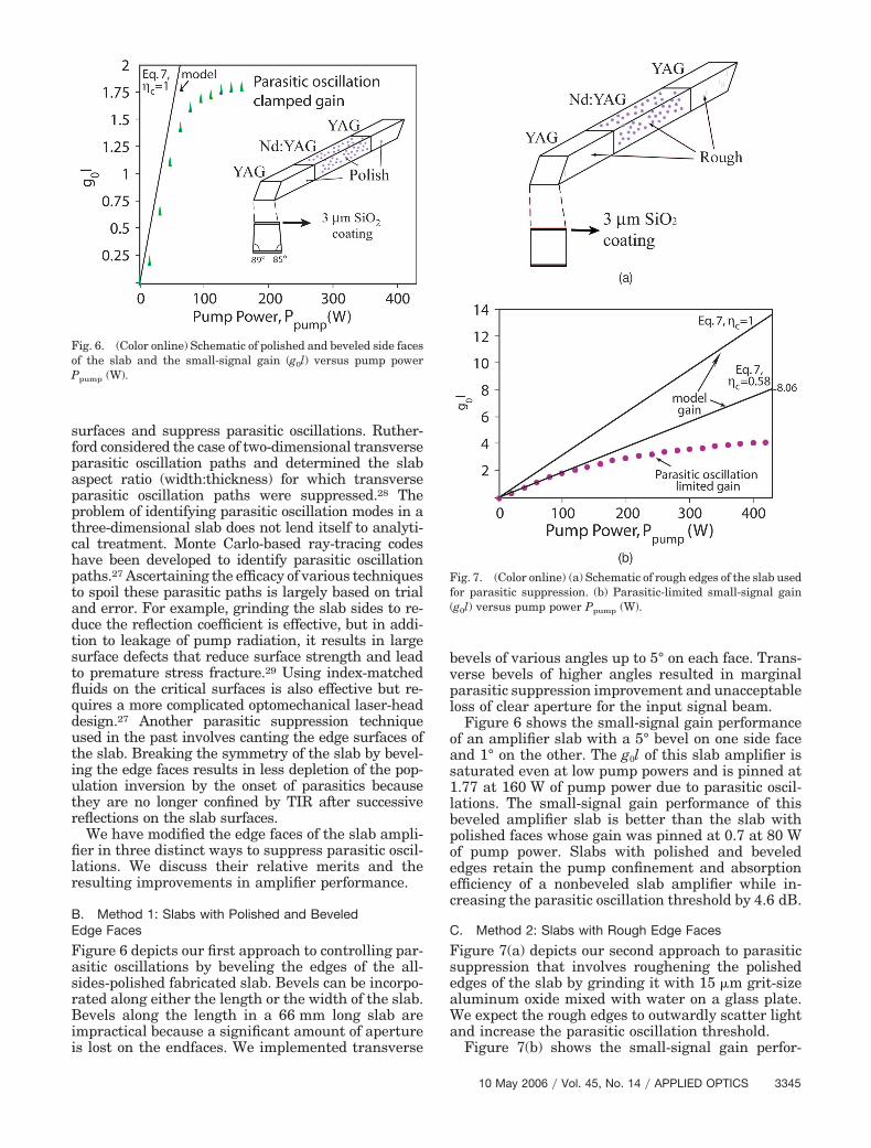
Figure 5 depicts the gain coefficient versus pumppower for the fabricated slab with polished edges.Visual inspection of the polished side faces of the slabunder pumping conditions confirms the expectednearly 100% pump confinement efficiency ��c � 1�.
Figure 5 shows that the g0l of this slab amplifier isclamped even at low pump powers and is pinned at0.7 at 80 W of pump power due to parasitic oscilla-tions. The all-sides-polished slab provides high reflec-tivity from the surfaces and permits parasitics toclamp the gain. Since the extracted power in a satu-rated amplifier is proportional to g0l this amplifierslab is unsuitable for efficient power extraction. Wenext focus on ways to increase the gain of the fabri-cated slab by suppressing parasitic oscillations.
4. Parasitic Oscillation Suppression
A. Background
A parasitic oscillation is basically a laser oscillatorwith a threshold dependent on optical path losses.The simplest parasitic oscillation occurs when theslab itself forms the cavity. The small-signal gaincoefficient �g0l�parasitic at parasitic oscillation thresholdis defined by
�g0l�parasitic � �1lT
ln� �i�1
N
Ri�, (13)
where Ri is the parasitic loop’s ith reflection coeffi-cient and lT is the parasitic loop’s total path length.27
To maximize �g0l�parasitic, the reflection coefficient fromeach slab surface should be minimized or effortsshould be taken to avoid closed optical paths thatlower �g0l�parasitic.
Several techniques have been investigated in thepast to minimize the reflection coefficient from the slab
Fig. 4. Expected amplifier gain coefficient (g0l) and single-passoutput power Pout (W) versus pump power Ppump (W). �c � 1, �abs
� 1, �q � 0.76, �p � 0.92, � � 28.33°, f � 0.26, wg � 300 �m, wt �1 mm2, Isat � 2500 kW�cm2, Pin � 30 W.
Fig. 5. (Color online) Schematic of the fabricated slab with pol-ished non-TIR (edge) faces and the small-signal gain versus pumppower Ppump (W).
3344 APPLIED OPTICS � Vol. 45, No. 14 � 10 May 2006
surfaces and suppress parasitic oscillations. Ruther-ford considered the case of two-dimensional transverseparasitic oscillation paths and determined the slabaspect ratio (width:thickness) for which transverseparasitic oscillation paths were suppressed.28 Theproblem of identifying parasitic oscillation modes in athree-dimensional slab does not lend itself to analyti-cal treatment. Monte Carlo-based ray-tracing codeshave been developed to identify parasitic oscillationpaths.27 Ascertaining the efficacy of various techniquesto spoil these parasitic paths is largely based on trialand error. For example, grinding the slab sides to re-duce the reflection coefficient is effective, but in addi-tion to leakage of pump radiation, it results in largesurface defects that reduce surface strength and leadto premature stress fracture.29 Using index-matchedfluids on the critical surfaces is also effective but re-quires a more complicated optomechanical laser-headdesign.27 Another parasitic suppression techniqueused in the past involves canting the edge surfaces ofthe slab. Breaking the symmetry of the slab by bevel-ing the edge faces results in less depletion of the pop-ulation inversion by the onset of parasitics becausethey are no longer confined by TIR after successivereflections on the slab surfaces.
We have modified the edge faces of the slab ampli-fier in three distinct ways to suppress parasitic oscil-lations. We discuss their relative merits and theresulting improvements in amplifier performance.
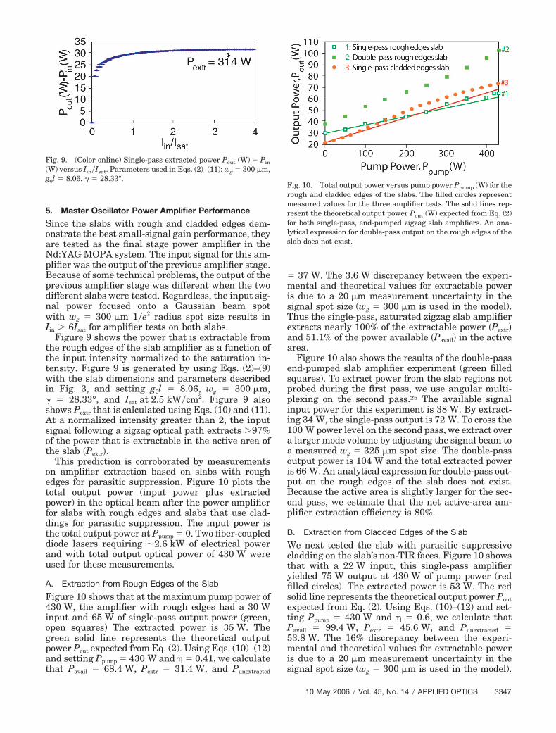
B. Method 1: Slabs with Polished and BeveledEdge Faces
Figure 6 depicts our first approach to controlling par-asitic oscillations by beveling the edges of the all-sides-polished fabricated slab. Bevels can be incorpo-rated along either the length or the width of the slab.Bevels along the length in a 66 mm long slab areimpractical because a significant amount of apertureis lost on the endfaces. We implemented transverse
bevels of various angles up to 5° on each face. Trans-verse bevels of higher angles resulted in marginalparasitic suppression improvement and unacceptableloss of clear aperture for the input signal beam.
Figure 6 shows the small-signal gain performanceof an amplifier slab with a 5° bevel on one side faceand 1° on the other. The g0l of this slab amplifier issaturated even at low pump powers and is pinned at1.77 at 160 W of pump power due to parasitic oscil-lations. The small-signal gain performance of thisbeveled amplifier slab is better than the slab withpolished faces whose gain was pinned at 0.7 at 80 Wof pump power. Slabs with polished and bevelededges retain the pump confinement and absorptionefficiency of a nonbeveled slab amplifier while in-creasing the parasitic oscillation threshold by 4.6 dB.
C. Method 2: Slabs with Rough Edge Faces
Figure 7(a) depicts our second approach to parasiticsuppression that involves roughening the polishededges of the slab by grinding it with 15 �m grit-sizealuminum oxide mixed with water on a glass plate.We expect the rough edges to outwardly scatter lightand increase the parasitic oscillation threshold.
Figure 7(b) shows the small-signal gain perfor-
Fig. 6. (Color online) Schematic of polished and beveled side facesof the slab and the small-signal gain (g0l) versus pump powerPpump (W).
Fig. 7. (Color online) (a) Schematic of rough edges of the slab usedfor parasitic suppression. (b) Parasitic-limited small-signal gain(g0l) versus pump power Ppump (W).
10 May 2006 � Vol. 45, No. 14 � APPLIED OPTICS 3345

mance of this slab amplifier. The parasitic oscillation-limited g0l is increased to 3.9. Visual inspection of theslab during amplifier tests suggested significantpump light loss. To quantify this loss, we draw a linerepresenting the extrapolated small-signal gain. Thisline represents the gain achievable if parasitic oscil-lations were negligible. This line can also be derivedby using �c as a fitting parameter and setting it equalto 0.58 in Eq. (7). Thus 42% of the pump light scattersout of the rough edges in the slab.
As the pump power is increased to 430 W, parasiticoscillations saturate the gain below the extrapolatedno-parasitic gain limit of 8.06. In a heavily saturatedamplifier where Iin �� Isat, the input beam will out-compete parasitic oscillations, saturate the small-signal gain, and extract power proportional to theno-parasitic g0l limit of 8.06 at 430 W of pump power.
The primary drawback of this slab amplifier is thelow pump confinement efficiency. The rough edgefaces lead to pump light loss but also cause significant
outward scatter of parasitic light. Parasitic suppres-sion via polishing and beveling the slab edges resultsin excellent confinement for pump light and unfortu-nately for signal parasitic modes as well. Our nextapproach to parasitic oscillation suppression is a hy-brid approach that takes advantage of the pump con-finement possible in the polished and beveled slaband the outward-scattering properties of the roughedges slab.
D. Method 3: Slabs with Polished, Beveled, and CladdedEdge Faces
Figure 8(a) shows our novel technique involving acladding on the edge surfaces to achieve enhancedparasitic suppression. The cladding consists of anoptical-grade epoxy that bonds a 100 �m thick pieceof silica to YAG. The index of refraction of the clad-ding, nclad, is selected to transmit the parasitic modesincident on the side faces at � � �crit while trappingthe pump rays that are incident on the faces at� � �crit. For a given slab width and thickness, anddivergence angle for the pump beam, we calculate theminimum angle �min at which pump rays are incidenton the side faces. �crit is set just below this value sothat all the pump rays are confined due to TIR andabsorbed in the doped region. We chose a claddingmaterial such that
�crit � sin�1�nclad
nYAG�. (14)
For our experimental conditions, we chose�crit � 60° and used an optical-grade epoxy with arefractive index of 1.55 as the cladding. To ensurethat rays in the cladding do not reenter the slabthrough TIR at the cladding–air interface, the silica’sinterface with air is roughened to enable outwardscattering.
Figure 8(b) shows the small-signal gain �g0l� versuspump power Ppump �W� in this slab. The small-signalgain coefficient reaches 4.5 at a pump power of340 W. We use �c as a fitted parameter, and by set-ting �c � 0.86 in Eq. (7), we find that 14% of pumplight scatters out of the cladding in the slab. Theextrapolated gain in this slab amplifier without par-asitic onset is 11.63 at 430 W of pump power. In aheavily saturated amplifier where Iin �� Isat, the in-put beam will extract power proportional to the ex-trapolated g0l of 11.63 at 430 W of pump power.
We summarize the small-signal gain measure-ments for the slab with rough sides (i.e., originalfabricated slab) and the slab with the cladding ap-plied. The extrapolated small-signal gain at a pumppower of 430 W is 8.06 for the slab with rough sides,and this improves to 11.63 for the slab with the clad-ding. The pump absorption efficiency is 58% on therough edges of the slab and 86% on the slabs with theparasitic suppression cladding. The significantly en-hanced small-signal gain in the slab with cladding onthe non-TIR faces offers the potential for increasedpower extraction in a saturated MOPA configuration.
Fig. 8. (Color online) (a) Illustration of slabs with claddings onedges for parasitic suppression. (b) Parasitic-limited small-signalgain (g0l) versus pump power Ppump (W).
3346 APPLIED OPTICS � Vol. 45, No. 14 � 10 May 2006
5. Master Oscillator Power Amplifier Performance
Since the slabs with rough and cladded edges dem-onstrate the best small-signal gain performance, theyare tested as the final stage power amplifier in theNd:YAG MOPA system. The input signal for this am-plifier was the output of the previous amplifier stage.Because of some technical problems, the output of theprevious amplifier stage was different when the twodifferent slabs were tested. Regardless, the input sig-nal power focused onto a Gaussian beam spotwith wg � 300 �m 1�e2 radius spot size results inIin � 6Isat for amplifier tests on both slabs.
Figure 9 shows the power that is extractable fromthe rough edges of the slab amplifier as a function ofthe input intensity normalized to the saturation in-tensity. Figure 9 is generated by using Eqs. (2)–(9)with the slab dimensions and parameters describedin Fig. 3, and setting g0l � 8.06, wg � 300 �m,� � 28.33°, and Isat at 2.5 kW�cm2. Figure 9 alsoshows Pextr that is calculated using Eqs. (10) and (11).At a normalized intensity greater than 2, the inputsignal following a zigzag optical path extracts �97%of the power that is extractable in the active area ofthe slab �Pextr�.
This prediction is corroborated by measurementson amplifier extraction based on slabs with roughedges for parasitic suppression. Figure 10 plots thetotal output power (input power plus extractedpower) in the optical beam after the power amplifierfor slabs with rough edges and slabs that use clad-dings for parasitic suppression. The input power isthe total output power at Ppump � 0. Two fiber-coupleddiode lasers requiring 2.6 kW of electrical powerand with total output optical power of 430 W wereused for these measurements.
A. Extraction from Rough Edges of the Slab
Figure 10 shows that at the maximum pump power of430 W, the amplifier with rough edges had a 30 Winput and 65 W of single-pass output power (green,open squares) The extracted power is 35 W. Thegreen solid line represents the theoretical outputpower Pout expected from Eq. (2). Using Eqs. (10)–(12)and setting Ppump � 430 W and � � 0.41, we calculatethat Pavail � 68.4 W, Pextr � 31.4 W, and Punextracted
� 37 W. The 3.6 W discrepancy between the experi-mental and theoretical values for extractable poweris due to a 20 �m measurement uncertainty in thesignal spot size (wg � 300 �m is used in the model).Thus the single-pass, saturated zigzag slab amplifierextracts nearly 100% of the extractable power �Pextr�and 51.1% of the power available �Pavail� in the activearea.
Figure 10 also shows the results of the double-passend-pumped slab amplifier experiment (green filledsquares). To extract power from the slab regions notprobed during the first pass, we use angular multi-plexing on the second pass.25 The available signalinput power for this experiment is 38 W. By extract-ing 34 W, the single-pass output is 72 W. To cross the100 W power level on the second pass, we extract overa larger mode volume by adjusting the signal beam toa measured wg � 325 �m spot size. The double-passoutput power is 104 W and the total extracted poweris 66 W. An analytical expression for double-pass out-put on the rough edges of the slab does not exist.Because the active area is slightly larger for the sec-ond pass, we estimate that the net active-area am-plifier extraction efficiency is 80%.
B. Extraction from Cladded Edges of the Slab
We next tested the slab with parasitic suppressivecladding on the slab’s non-TIR faces. Figure 10 showsthat with a 22 W input, this single-pass amplifieryielded 75 W output at 430 W of pump power (redfilled circles). The extracted power is 53 W. The redsolid line represents the theoretical output power Poutexpected from Eq. (2). Using Eqs. (10)–(12) and set-ting Ppump � 430 W and � � 0.6, we calculate thatPavail � 99.4 W, Pextr � 45.6 W, and Punextracted �53.8 W. The 16% discrepancy between the experi-mental and theoretical values for extractable poweris due to a 20 �m measurement uncertainty in thesignal spot size (wg � 300 �m is used in the model).
Fig. 9. (Color online) Single-pass extracted power Pout (W) Pin
(W) versus Iin�Isat. Parameters used in Eqs. (2)–(11): wg � 300 �m,g0l � 8.06, � � 28.33°.
Fig. 10. Total output power versus pump power Ppump (W) for therough and cladded edges of the slabs. The filled circles representmeasured values for the three amplifier tests. The solid lines rep-resent the theoretical output power Pout (W) expected from Eq. (2)for both single-pass, end-pumped zigzag slab amplifiers. An ana-lytical expression for double-pass output on the rough edges of theslab does not exist.
10 May 2006 � Vol. 45, No. 14 � APPLIED OPTICS 3347
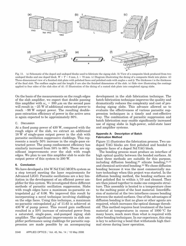
On the basis of the measurements on the rough edgesof the slab amplifier, we expect that double passingthis amplifier with wg � 300 �m on the second passwill result in 25 W of additional extracted power toreach 98 W output power. The resulting double-pass extraction efficiency of power in the active areais again expected to be approximately 80%.
C. Discussion
At a fixed pump power of 430 W, compared with therough edges of the slab, we extract an additional18 W of single-pass output power in the slab withparasitic oscillation suppressive claddings. This rep-resents a nearly 50% increase in the single-pass ex-tracted power. The pump confinement efficiency hassimilarly increased from 58% to 86%. These are sig-nificant improvements over the slab with roughedges. We plan to use this amplifier slab to scale theoutput power of this system to 200 W.
6. Conclusion
We have developed a 104 W Nd:YAG MOPA system asa step toward meeting the laser requirements forAdvanced LIGO. Parasitic oscillations are a key lim-itation in the development of an efficient power am-plifier for this system. We investigated three differentmethods of parasitic oscillation suppression. Slabswith rough edges have a maximum no-parasitic ex-trapolated g0l of 8.06. We improved this result byincorporating a novel technique involving claddingson the edge faces. Using this technique, a maximumno-parasitic extrapolated g0l of 11.63 is achieved at430 W of pump power. This record gain coefficientresulted in a 50% increase of extracted power froma saturated, single-pass, end-pumped zigzag slabamplifier. The significant improvements in slab am-plifier performance using claddings for parasitic sup-pression are made possible by an accompanying
development in the slab fabrication technique. Thebatch fabrication technique improves the quality anddramatically reduces the complexity and cost of pro-ducing zigzag slabs. This advance allowed us toevaluate the effectiveness of various parasitic sup-pression techniques in a timely and cost-effectiveway. The combination of parasitic suppression andbatch fabrication may enable significantly increaseduse of zigzag slabs in high-power, solid-state laserand amplifier systems.
Appendix A: Description of BatchFabrication Method
Figure 11 illustrates the fabrication process. Two un-doped YAG blocks are first polished and bonded toopposite faces of a doped Nd:YAG block.
The bonding process must produce an interface ofhigh optical quality between the bonded surfaces. Atleast three methods are suitable for this purpose,including diffusion bonding,30 silicate bonding,31,32
and chemical-activated bonding.33 We chose diffusionbonding because it was the most commercially ma-ture technology when this project was started. In thediffusion bonding method, the bonding surfaces arefirst polished flat to within �10 and cleaned. Theyare then joined together to make one composite struc-ture. This assembly is heated to a temperature closeto the melting point of the host material. Interdiffu-sion of material at the two interfaces causes bondingbetween the mated surfaces. One of the advantages ofdiffusion bonding is that no glues or other agents arerequired, which increases the optical damage thresh-old. This method requires heat treatment of the lasermaterial at temperatures in excess of 1000 °C formany hours, much more than what is required withother bonding techniques. In our experience, this stepis key to achieving a bond that withstands high ther-mal stress during laser operation.
Fig. 11. (a) Schematic of the doped and undoped blocks used to fabricate the zigzag slab. (b) View of a composite block produced from twoundoped blocks and one doped block. W � T � 8 mm, L � 70 mm. (c) Diagram illustrating the dicing of a composite block into plates. (d)Three-dimensional view of a finished slab plate with polished faces and polished ends with angles � and . The thickness t is the thicknessof the final slab. The endface angles and the length S are also the finished dimensions of the slab. (e) Side view illustrating the coatingsapplied to four sides of the slab slice of (d). (f) Illustration of the dicing of a coated slab plate into completed zigzag slabs.
3348 APPLIED OPTICS � Vol. 45, No. 14 � 10 May 2006

Figure 11(b) shows the composite block followingthe diffusion bonding step. The composite block hasthe length L, width W, and thickness T required forproducing the desired number of zigzag slabs. For theamplifiers developed in this work, the blocks were8 mm � 8 mm on the sides with a total compositelength L of 70 mm.
Next, the interfaces delimiting the doped and un-doped regions of the slab sandwich are visually in-spected to ensure that they are free of defects. Toascertain whether the composite block can withstandthe stresses induced during further fabrication steps,a bond strength test is especially useful. The strengthof the bond also gives an indication of the amount ofthermal stress the finished slab can withstand duringlaser operation. A shear strength test can be appliedto evaluate the force required to break the bond. Weunfortunately did not perform shear strength tests onthe Nd:YAG composite blocks but instead hadstrength tests performed commercially on similarlyfabricated Yb:YAG slab plates. These plates, similarto the Nd:YAG plates shown in Fig. 11(d), were11 mm � 5 mm � 0.4 mm. The test setup involves anImada DPS-110 load cell on an Imada test stand witha custom clamping mechanism. The tests showedthat diffusion-bonded Yb:YAG plates fractured in thebulk with a 2.2 kg mass object exerting pressure overa 2 mm � 2 mm area on the plates’ large surfaces.Since the block did not break at the bond interface,we infer that the diffusion-bonded blocks are me-chanically as strong as bulk YAG. We did not performfurther tests on diffusion-bonded blocks as diffusion-bonded (produced by Onyx Optics) slab lasers hadbeen commercially operated at the 400 W pumppower levels.11
Figure 11(c) illustrates the next step in which theslab sandwich is sliced perpendicular to its thicknessto produce a number of slab plates with thickness t.This step creates multiple minute fractures in theslab plates, which leads to undesirable reduction inthe fracture resistance. However, the residual micro-cracks can be removed by taking off 150 �m of ma-terial from the plate while grinding and polishing. Atthe end of this polishing step, the two large surfacesof each slab plate are mechanically strong and have aflatness of �10 to ensure TIR with minimal distor-tion of the beam phase front. The variation in thick-ness t should be less than 0.01 mm to preventclipping of the zigzagging signal beam at the outputendface.
Next, the faces at both ends of each slab plate arepolished at an angle to enable coupling of the signalbeam into the zigzag slab and the pump radiationthrough TIR. Figure 11(d) shows plates with an apexangle � at one end and at the other end. The angles’values are chosen after careful simulation of thepropagation of the pump and signal beams throughthe slab. During this processing step care must betaken to avoid chips on the end surfaces near the tips,which would increase the chance of catastrophic sur-face damage under high-power operation. This fabri-cation step also determines the total length S of the
undoped and doped regions. The side cross-sectionalview of this slab plate is the same as that of the finalzigzag slab.
The finished slab plates are then coated on foursurfaces as illustrated in Fig. 11(e). A SiO2 AR coat-ing is deposited on the plates’ large surfaces. Theyform the TIR surfaces for the finished slabs. Theend-coupling faces are AR coated for both s and p
wavelengths to minimize loss of the amplified signalas well as to alternatively pump through the endfaceswithout loss.
Figure 11(f) illustrates the final dicing of a coatedslab plate into individual zigzag slabs. The slab plateis diced and polished perpendicular to the TIR sur-faces and along the length of the slab. This step de-fines the width w of each zigzag slab, as well as thesurface quality of the sidewalls. The properties of thesidewalls can later be tailored to reduce the possibil-ity of parasitic oscillations. At this point the zigzagslab is ready to be used in a laser or an amplifier.
We began this fabrication process with three com-posite blocks that were diced into plates, polished,coated, and finally diced to achieve the final slabdimensions. These plates were then finally diced toproduce the finished slabs. By starting with an8 mm � 8 mm � 70 mm bonded block, we were ableto fabricate 30 slabs. We optically tested 10 slabamplifiers and they performed identically. We believethis performance will be maintained as the fabrica-tion process is scaled up to produce more slabs. An-other advantage of this fabrication process stemsfrom the fact that most of the intermediate stepsinvolved working with material that had large sur-face areas. This fact resulted in mechanically stron-ger diffusion-bonded blocks, the surface quality (i.e.,flatness and parallelism requirements) of the pol-ished surfaces was better controlled, and the reflec-tivity of the coatings was more uniform across thesurfaces.
The polishing and dicing were performed by onecommercial vendor and the coating operations by an-other. Both vendors needed to machine special toolsthat held the slab plates while they were being diced,polished, and coated. Because these tools were tiny(i.e., �1 mm critical dimensions), their machining re-quired special expertise and resulted in higher thanaverage manufacturing costs. The coating steps werealso delicate operations because, while one of the sur-faces was being coated, all the others needed to belithographically masked. This was done to ensurethat there was no spillover of coating compoundsmeant for one surface onto a surface that is designedto have completely different optical properties.Table 1 summarizes the fabrication steps and costs.
The cost of each processing step can be divided intononrecurring and incremental costs. The polishingand coating steps require an initial investment inprecision tools in addition to the polishing saw andthe coating chamber. When relatively few slabs arefabricated (as is true in our case), Table 1 shows thatfixed costs form nearly 50% of the total. However, asthe fabrication process is scaled, the fixed costs form
10 May 2006 � Vol. 45, No. 14 � APPLIED OPTICS 3349

a small fraction of the total. Improved efficiencieswithin the polishing and coating steps result in amuch smaller net cost per slab. As Table 1 indicates,the coating step is comparatively more expensive.However, the cost for this step will drop two to threetimes if 1000 plates are coated. Similarly, improvedefficiencies in the other processing steps will result in�$400�slab for truly large-scale manufacturing ofslabs.
Finally, it is important to note that fabricatingsuch small slabs would not be possible in a one-by-onefabrication process. Bonding, polishing, and coatingsuch YAG across such tiny dimensions and highlength-to-thickness aspect ratios is extremely diffi-
cult and prohibitively expensive. As a further illus-tration of this fabrication process, we have producedYb:YAG slabs following the above recipe. Theseslabs (0.4 mm � 0.4 mm � 11 mm, Fig. 12) form theworld’s smallest slab laser and are useful as pulsedamplifiers for remote sensing applications. This im-plementation has allowed slab laser devices to scaletoward dimensions that were previously only theprovince of optical fibers.
We have presented a method for batch fabricationof Nd:YAG slabs for use in solid-state lasers. Thesteps include bonding undoped YAG to either side ofa doped YAG block to form a sandwich and dicing thesandwich to provide slices. Two of the surfaces of eachslice are cut, ground, and polished as TIR surfaces,then diced perpendicular to the TIR surfaces to pro-vide many zigzag slabs at reduced cost. Thirty slabswere obtained in our implementation of this batchfabrication process. The cost per slab is approxi-mately $1700, which is a small fraction of the overallcost of a typical laser system. By using larger blocksof YAG and Nd:YAG as starter material, and goinginto mass production (i.e., producing �1000 slabs),the cost per slab can be less than $600. This fabrica-tion procedure can be implemented in almost anycrystalline or ceramic host material and dopant(s). Aprerequisite is that the material should have the req-uisite mechanical strength to tolerate the stressesoften induced in the slabs during the coating, cutting,and polishing steps. We believe that this slab fabri-cation process will enable the low-cost manufactureof laser slabs and make them suitable for widespreaduse in high-power solid-state lasers and amplifiers.
Fig. 12. (Color online) World’s smallest Yb:YAG slab laser fabri-cated by the batch fabrication process (0.4 mm � 0.4 mm � 11mm).
Table 1. Summary of Batch Fabrication Steps and Cost per Operation
StepBrief Description of the Various
Slab Fabrication Steps Cost ($)Cost perSlab ($)
Cost per Slabfor 1000
Slabs ($)a
1 Procure Nd:YAG and YAG rawmaterial and diffusion bondthe doped and undoped pieces.The two resultant pieces were8 mm � 8 mm � 7 cm blocks[Fig. 11(b)].
10,000 333 100
Material costs 4620
Bonding cost for two pieces 5380
2 Perform all dicing and polishingoperations to make plates thatmeet all slab dimensionspecifications, except for thewidth. Total of six plates weremanufactured [Figs. 11(c) and11(d)].
17,000 566 100
Cost of tools 8500
Cost of dicing and polishing plates 8500
3 Perform all the coatingoperations [Fig. 11(e)].
22,500 750 375Cost of tools 11,000Cost of four coating runs 11,500
4 Dice and polish the coated slabplates to obtain a multiplicityof slabs having the requiredwidth [Fig. 11(f)].
1000 33 25
Total 30 slabs produced 50,500 1682 600
aBased on estimates provided by vendors.
3350 APPLIED OPTICS � Vol. 45, No. 14 � 10 May 2006

The authors thank Todd Rutherford for helpfuldiscussions in the early phase of this work, TedJudd of Crystal River Optics for his skill and pa-tience in fabricating numerous slabs, Gary Debell ofMLD Technologies for helpful discussions on coat-ing techniques and implementing them, and KarelUrbanek for lots of experimental help in the dem-onstration of the 100 W MOPA system.15 This workwas supported in part by National Science Founda-tion grants PHY-0140297 and PHY-9210038 and inpart by the U.S. Army Research Office under grantDAAD19-02-1-0184.
References1. W. Wiechmann, T. J. Kane, D. Haserot, F. Adams, G. Truong,
and J. Kmetec, “20 W diode-pumped single-frequency Nd:YAGMOPA for the Laser Interferometer Gravitational Wave Ob-servatory,” in Conference on Lasers and Electro-Optics, Vol. 6of OSA Technical Digest Series (Optical Society of America,1998), p. 432.
2. LIGO II Conceptual Project Book (1999), www.ligo.org/pdf/M990288-A.pdf.
3. M. Frede, R. Wilhelm, M. Brendel, C. Fallnich, F. Seifert, B.Willke, and K. Danzmann, “High power fundamental modeNd:YAG laser with efficient birefringence compensation,” Opt.Express 12, 3581–3589 (2004).
4. Y. Jeong, J. Nilsson, J. K. Sahu, D. B. S. Soh, C. Alegria, P.Dupriez, C. A. Codemard, D. N. Payne, R. Horley, L. M. B.Hickey, L. Wanzcyk, C. E. Chryssou, J. Alvarez-Chavez, andP. W. Turner, “Single-frequency, single-mode, plane-polarizedytterbium-doped fiber master oscillator power amplifier sourcewith 264 W of output power,” Opt. Lett. 30, 459–462 (2005).
5. W. S. Martin and J. P. Chernoch, “Multiple internal reflectionface pumped laser,” U.S. patent 3,633,126 (4 January 1972).
6. A. Giesen, H. Hugel, A. Voss, K. Wittig, U. Brauch, and H.Opower, “Scalable concept for diode pumped high power la-sers,” Appl. Phys. B 58, 365–372 (1994).
7. C. Stewen, K. Contag, M. Larionov, A. Giesen, and H. Hugel,“A 1-kW cw thin disc laser,” IEEE J. Sel. Top. Quantum Elec-tron. 6, 650–657 (2000).
8. J. M. Eggleston, T. J. Kane, K. Kuhn, J. Unternahrer, andR. L. Byer, “The slab geometry laser. Part 1: Theory,” IEEE J.Quantum Electron. 20, 289–301 (1984).
9. R. J. Shine, Jr., A. J. Alfrey, and R. L. Byer, “40 W CW,TEM00-mode, diode-laser-pumped, Nd:YAG miniature-slab la-ser,” Opt. Lett. 20, 459–462 (1995).
10. T. Kane, R. Eckardt, and R. Byer, “Reduced thermal focusingand birefringence in zigzag slab geometry crystalline lasers,”IEEE J. Quantum Electron. 19, 1351–1354 (1983).
11. G. D. Goodno, S. Palese, J. Harkenrider, and H. Injeyan, “Highaverage-power Yb:YAG end-pumped zig-zag slab laser,” in Ad-vanced Solid-State Lasers, C. Marshall, ed., Vol. 50 of OSATrends in Optics and Photonics Series (Optical Society ofAmerica, 2001), pp. 2–4.
12. T. S. Rutherford, W. M. Tulloch, S. Sinha, and R. L. Byer,“Yb:YAG and Nd:YAG edge-pumped slab lasers,” Opt. Lett. 26,986–989 (2001).
13. A. D. Farinas, E. K. Gustafson, and R. L. Byer, “Design andcharacterization of a 5.5 W, cw, injection-locked fiber-coupled,laser-diode-pumped Nd:YAG miniature-slab laser,” Opt. Lett.19, 114–117 (1994).
14. G. D. Goodno, H. Komine, S. J. McNaught, B. Weiss, S. Red-mond, W. Long, R. Simpson, E. Cheung, D. Howland, P. Epp,M. Weber, M. McClellan, J. Sollee, and H. Injeyan, “19-kWphase-locked MOPA laser array,” in Advanced Solid-StatePhotonics, OSA Trends in Optics and Photonics Series (OpticalSociety of America, 2006), paper MA2.
15. S. Saraf, S. Sinha, A. K. Sridharan, and R. L. Byer, “100 W,single frequency, low-noise, diffraction-limited beam from anNd:YAG end-pumped slab MOPA for LIGO,” in AdvancedSolid-State Photonics (Nineteenth Topical Meeting and Table-top Exhibit), Postdeadline Proceedings, Vol. 94 of OSA Trendsin Optics and Photonics Series (Optical Society of America,2004).
16. B. Willke, N. Uehara, E. K. Gustafson, R. L. Byer, P. King, S.Seel, and R. L. Savage, Jr., “Spatial and temporal filtering of a10-W Nd:YAG laser with a Fabry–Perot ring-cavity premodecleaner,” Opt. Lett. 23, 1704–1706 (1998).
17. S. Saraf, K. Urbanek, R. L. Byer, and P. J. King, “Quantum noisemeasurements in a continuous-wave laser-diode-pumpedNd:YAG saturated amplifier,” Opt. Lett. 30, 1195–1197 (2005).
18. A. E. Siegman, Lasers (University Science, 1987).19. Y. Chen, B. Chen, M. K. R. Patel, A. Kar, and M. Bass, “Cal-
culation of thermal gradient induced stress birefringence inslab lasers. II,” IEEE J. Quantum Electron. 40, 917–927(2004).
20. Y. Chen, B. Chen, M. K. R. Patel, and M. Bass, “Calculation ofthermal gradient induced stress birefringence in slab lasers.I,” IEEE J. Quantum Electron. 40, 909–916 (2004).
21. J. Eggleston, L. M. Frantz, and H. Injeyan, “Derivation of theFranz-Nodvik equation for zig-zag optical path, slab geometrylaser amplifiers,” IEEE J. Quantum Electron. 25, 1855–1862(1989).
22. L. M. Franz and J. S. Nodvik, “Theory of pulse propagation ina laser amplifier,” J. Appl. Phys. 34, 2346–2349 (1963).
23. T. Y. Fan, “Heat generation in Nd:YAG and Yb:YAG,” IEEE J.Quantum Electron. 29, 1457–1459 (1993).
24. J. Fryer, Microcooling Concepts, Inc., 7522 Slater Ave., Suite122, Huntington Beach, Calif. 92647 (custom design).
25. T. J. Kane and R. L. Byer, “62-dB-gain multiple-pass slabgeometry Nd:YAG amplifier,” Opt. Lett. 11, 216–219 (1986).
26. W. Koechner, Solid-State Laser Engineering, 5th ed.(Springer-Verlag, 1999).
27. D. C. Brown, D. P. Benfey, W. J. Gehm, D. H. Holmes, andK. K. Lee, “Parasitic oscillations and amplified spontaneousemission in face-pumped total internal reflection lasers,” Proc.SPIE 736, 74–83 (1987).
28. T. Rutherford, “An edge-pumped Yb:YAG laser and phasedarray resonator,” Ph.D. dissertation (Stanford University,2001).
29. W. F. Krupke, M. D. Shinn, J. E. Marion, J. A. Caird, and S. E.Stokowski, “Spectroscopic, optical, and thermomechanicalproperties of neodymium- and chromium-doped gadoliniumscandium gallium garnets,” J. Opt. Soc. Am. B 3, 102–114(1986).
30. H. Meissner, “Composites made from single crystal sub-stances,” U.S. patent 5,441,803 (15 August 1995).
31. D. Z. Gwo, “Hydroxide-catalyzed bonding,” U.S. patent6,548,176 (15 April 2003).
32. D. Z. Gwo, “Ultra precision and reliable bonding method,” U.S.patent 6,284,085 (4 September 2001).
33. N. Traggis, Precision Photonics Corporation, Boulder, Colo.(personal communication, 2005).
10 May 2006 � Vol. 45, No. 14 � APPLIED OPTICS 3351