zte mg3030 module technical specifications - · pdf filegsm-mg3030 module product zte mg3030...
TRANSCRIPT

GSM-MG3030 module product
ZTE MG3030 Module Technical Specifications
VERSION V1.2
ZTE CORPORATION
This manual is also applicable for MG3036 module.

GSM-MG3030 module products
Foreword
Summary
The corresponding product to this document is MG3030 and MG3036 modules. It introduces the
appearance, hardware framework, functions, technical specifications and relevant test standard of
MG3030 module as an example, which is used for supporting design reference to hardware
engineers and product designers.
Object readers
This document is mostly suitable for engineers as below:
System designers
Product engineers
Hardware engineers
Software engineers
Test engineers
Brief
This document contains 7 chapters, as following:
chapter contents
1Summary Background, concepts and applications of MG3030
2Abbreviation Abbreviations appeared in this document
3 appearance and framework Appearance figure of MG3030 module
4 functions Basic functions of MG3030 module
5 interfaces Basic interfaces of MG3030 module
6 Technical specifications Introduce particular technical specifications of MG3030 module
7 reliability test standard Introduce the reliability test standard of MG3030 module.
8 EMC/EMI standard Introduce EMC/EMI standard of MG3030 module
Modified records
Modified records accumulate update notes every time. The latest document version includes all
update contents previously.
Document version V1.2 (2007-08-17)
Released formally for the 3rd time, the update contents include:
Change ME for MG.
Document version V1.1 (2007-07-09)
Released formally for the 2st time, the update contents include:
Add this manual is also applicable for MG3036 module.
3

GSM-MG3030 module products
Modify MG3030’s frequency.
Modify 6.Reliability test standard
Document version V1.0 (2007-05-31)
Released formally for the 1st time
4

GSM-MG3030 module products
Table of contents
1 SUMMARY .......................................................................................................................................8
2 ABBREVIATION ...............................................................................................................................8
3 APPEARANCE AND FRAMEWORK ..............................................................................................10
4 FUNCTIONS .................................................................................................................................. 11
5 INTERFACES.................................................................................................................................12
6 TECHNICAL SPECIFICATIONS.....................................................................................................13
6.1 TECHNICAL PARAMETERS ......................................................................................................................13
6.2 RF EMISSION .......................................................................................................................................13
6.2.1 Frequency and phase bias..........................................................................................................13
6.2.2 Frequency and phase bias under multi-path interference ..........................................................13
6.2.3 Tx peak value power and pulse envelop timing..........................................................................14
6.2.4 TX output spectrum.....................................................................................................................17
6.3 RF RECEIVING......................................................................................................................................18
6.3.1 Reference sensitivity...................................................................................................................19
6.3.2 Available input level.....................................................................................................................20
6.3.3 Co-channel suppression .............................................................................................................20
6.3.4 Adjacent channel suppression ....................................................................................................21
6.3.5 Intermodulation suppression.......................................................................................................22
6.3.6 Blocking and spurious respond...................................................................................................22
6.4 RECOMMENDATION OF ANTENNA SPECS .................................................................................................24
6.5 POWER SUPPLY....................................................................................................................................25
6.5.1 Input voltage................................................................................................................................25
6.6 WORKING CONDITIONS .........................................................................................................................25
7 RELIABILITY TEST STANDARD....................................................................................................25
7.1 LOW TEMPERATURE RUNNING EXPERIMENT ............................................................................................25
7.2 LOW TEMPERATURE STORAGE EXPERIMENT ...........................................................................................25
7.3 HIGH TEMPERATURE RUNNING EXPERIMENT ...........................................................................................25
7.4 HIGH TEMPERATURE STORAGE EXPERIMENT ..........................................................................................25
7.5 HIGH TEMPERATURE, HIGH HUMIDITY EXPERIMENT..................................................................................26
7.6 HIGH-LOW TEMPERATURE STRIKING EXPERIMENT ...................................................................................26
8 EMC/EMI TEST STANDARD..........................................................................................................26
8.1 STATIC DISCHARGE ESD INTERFERENCE IMMUNITY EXPERIMENT .......................................................26
8.2 RF ELECTROMAGNETIC EMISSION INTERFERENCE IMMUNITY EXPERIMENT................................................26
8.3 ELECTRICAL FAST TRANSIENT/BURST IMMUNITY EXPERIMENT ..................................................................27
8.4 LIGHTNING AND SURGE STRIKE IMMUNITY EXPERIMENT ...........................................................................27
8.5 RF ELECTROMAGNETIC FIELD CONDUCTION INTERFERENCE IMMUNITY EXPERIMENT .................................27
8.6 RADIATED DISTURBANCE EXPERIMENT ...................................................................................................28
8.7 CONDUCTED DISTURBANCE EXPERIMENT ...............................................................................................28
5

GSM-MG3030 module products
TABLE OF FIGURES Figure 3-1 appearance of MG3030 module......................................................................................................... 10
Figure6-1 Power/time envelop framework under normal test condition ............................................................. 16
Figure6-2 power/time envelop framework under ultra test condition ................................................................. 16
6

GSM-MG3030 module products
TABLES Table 4-1 Main functions and features........................................................................................................... 11
Table 5-1 Interfaces of the modules............................................................................................................... 12
Table 6-1 Technical parameters ........................................................................................................................... 13
Table6-2 frequency bias....................................................................................................................................... 14
Table6-3 error rate tested in each channel of GSM 850 and GSM 900............................................................... 19
Table6-4 error rate tested in each channel of DCS 1800 and PCS 1900 ............................................................. 19
Table6-5 error rate tested in each channel of GSM 850 and GSM 900............................................................... 20
Table6-6 error rate tested in each channel of CS 1800 and PCS 1900 ................................................................ 20
Table6-7 error rate limit and minimum quantity of samples in each full-speed channel..................................... 21
Table 6-8 error rate limit and minimum quantity of samples in each half-speed channel of GSM 850 and GSM
900....................................................................................................................................................... 21
Table6-9 error rate limit and minimum quantity of samples in each half-speed channel of DCS 1800 and PCS
1900..................................................................................................................................................... 21
Table6-10 the useless signal level of GSM 900 and DCS 1800 .......................................................................... 23
Table6-11 The useless signal level of PCS 1900 ................................................................................................. 23
Table6-12 The useless signal level of GSM 850 ................................................................................................. 23
Table6-13 Error rate limit and minimum quantity of samples in each channel ................................................... 23
Table6-14 recommended antenna specs .............................................................................................................. 24
Table6-15 input voltage ....................................................................................................................................... 25
Table8-1 static experiment level.......................................................................................................................... 26
Table8-2 emission anti-interference experiment level......................................................................................... 26
Table8-3 Electrical fast-changed pulse group anti-interference experiment level............................................... 27
Table8-4 Lightning and surge strike anti-interference experiment...................................................................... 27
Table8-5 conduction anti-interference experiment level ..................................................................................... 27
7

GSM-MG3030 module products
1 Summary
ZTE MG3030 and MG3036 modules is GSM/GPRS wireless modules, with abundant voice, SMS,
data service functions and so on. Since designed with stamp holes connection and thinner body, their
current became lower. The modules can be applied in handsets, wireless data cards, USB modem,
trackers, etc.
This document take MG3030 module as an example, introduces the appearance, hardware
framework, functions, technical specifications and relevant test standards for module in detail.
2 Abbreviation
Abbr. Full name
ADC Analog-Digital Converter
AFC Automatic Frequency Control
AGC Automatic Gain Control
ARFCN Absolute Radio Frequency Channel Number
ARP Antenna Reference Point
ASIC Application Specific Integrated Circuit
BER Bit Error Rate
BTS Base Transceiver Station
CDMA Code Division Multiple Access
CDG CDMA Development Group
CS Coding Scheme
CSD Circuit Switched Data
CPU Central Processing Unit
DAI Digital Audio interface
DAC Digital-to-Analog Converter
DCE Data Communication Equipment
DSP Digital Signal Processor
DTE Data Terminal Equipment
DTMF Dual Tone Multi-Frequency
DTR Data Terminal Ready
EFR Enhanced Full Rate
EGSM Enhanced GSM
EMC Electromagnetic Compatibility
EMI Electro Magnetic Interference
ESD Electronic Static Discharge
ETS European Telecommunication Standard
FDMA Frequency Division Multiple Access
FR Full Rate
8

GSM-MG3030 module products
GPRS General Packet Radio Service
GSM Global Standard for Mobile Communications
HR Half Rate
IC Integrated Circuit
IMEI International Mobile Equipment Identity
ISO International Standards Organization
ITU International Telecommunications Union
LCD Liquid Crystal Display
LED Light Emitting Diode
MCU Machine Control Unit
MMI Man Machine Interface
MS Mobile Station
PCB Printed Circuit Board
PCL Power Control Level
PCS Personal Communication System
PDU Protocol Data Unit
PLL Phase Locked Loop
PPP Point-to-point protocol
RAM Random Access Memory
RF Radio Frequency
ROM Read-only Memory
RMS Root Mean Square
RTC Real Time Clock
SIM Subscriber Identification Module
SMS Short Message Service
SRAM Static Random Access Memory
TA Terminal adapter
TDMA Time Division Multiple Access
TE Terminal Equipment also referred it as DTE
UART Universal asynchronous receiver-transmitter
UIM User Identifier Management
USB Universal Serial Bus
VSWR Voltage Standing Wave Ratio
ZTE ZTE Corporation
9

GSM-MG3030 module products
3 Appearance and framework
The lands are distributed at both short sides since MG3030 module adopts stamp-hole connection.
There are 18 pins at each side. Appearance of MG3030 is as following figure 3-1:
Figure 3-1 appearance of MG3030 module
Dimension length x width x height 38.0 mm x 28.0mm x 2.3mm
Weight 8g
10
GSM-MG3030 module products
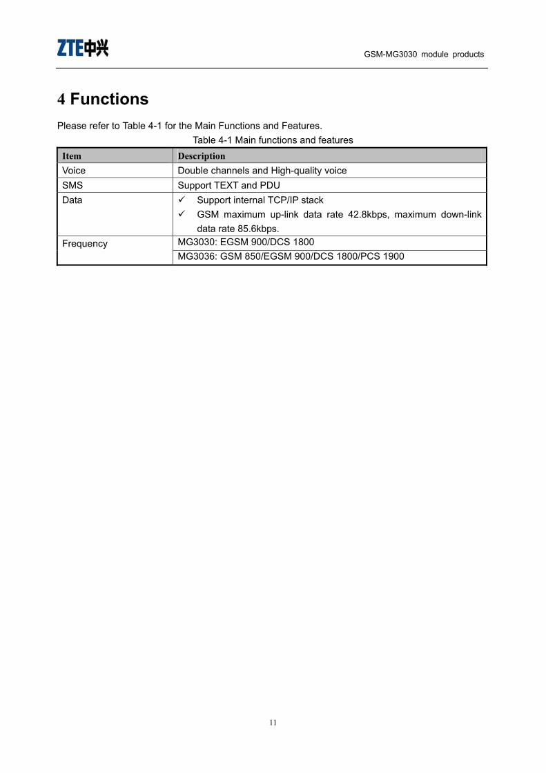
4 Functions
Please refer to Table 4-1 for the Main Functions and Features.
Table 4-1 Main functions and features
Item Description
Voice Double channels and High-quality voice
SMS Support TEXT and PDU
Data ! Support internal TCP/IP stack
! GSM maximum up-link data rate 42.8kbps, maximum down-link
data rate 85.6kbps.
MG3030: EGSM 900/DCS 1800 Frequency
MG3036: GSM 850/EGSM 900/DCS 1800/PCS 1900
11

GSM-MG3030 module products
5 Interfaces
Please refer to Table 5-1 for the Interfaces. Table 5-1 Interfaces of the modules
Item Description
UART interface Download software to update
Data communication
Maximum data rate 230.4kbps through the port
Audio interface Double audio I/O channel.
SIM card interface SIM card interface
Antenna interface 50 Ohm input impedance control
12
GSM-MG3030 module products
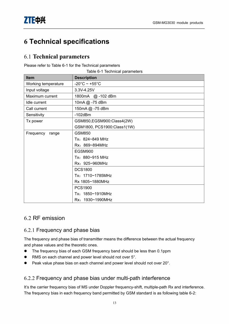
6 Technical specifications
6.1 Technical parameters
Please refer to Table 6-1 for the Technical parameters
Table 6-1 Technical parameters
Item Description
Working temperature -20°C ~ +55°C
Input voltage 3.3V-4.25V
Maximum current 1800mA @ -102 dBm
Idle current 10mA @ -75 dBm
Call current 150mA @ -75 dBm
Sensitivity -102dBm
Tx power GSM850,EGSM900:Class4(2W)
GSM1800, PCS1900:Class1(1W)
GSM850
Tx 824~849 MHz
Rx 869~894MHz
EGSM900
Tx 880~915 MHz
Rx 925~960MHz
DCS1800
Tx 1710~1785MHz
Rx 1805~1880MHz
Frequency range
PCS1900
Tx 1850~1910MHz
Rx 1930~1990MHz
6.2 RF emission
6.2.1 Frequency and phase bias
The frequency and phase bias of transmitter means the difference between the actual frequency
and phase values and the theoretic ones.
The frequency bias of each GSM frequency band should be less than 0.1ppm
RMS on each channel and power level should not over 5°.
Peak value phase bias on each channel and power level should not over 20°.
6.2.2 Frequency and phase bias under multi-path interference
It’s the carrier frequency bias of MS under Doppler frequency-shift, multiple-path Rx and interference.
The frequency bias in each frequency band permitted by GSM standard is as following table 6-2:
13

GSM-MG3030 module products
Table6-2 frequency bias
GSM 850 and GSM 900 DCS 1800 PCS 1900
Spread
condition
Allowable
frequency bias
Spread
condition
Allowable
frequency bias
Spread
condition
Allowable
frequency bias
RA250 ±300Hz RA130 ±400Hz RA130 ±420Hz
HT100 ±180Hz HT100 ±350Hz HT100 ±370Hz
TU50 ±160Hz TU50 ±260Hz TU50 ±280Hz
TU3 ±230Hz TU1.5 ±320Hz TU1.5 ±330Hz
6.2.3 Tx peak value power and pulse envelop timing
Carrier peak value power of transmitter is the average value on a burst pulse’s useful
information bit time.
Outburst pulse timing is the interval between Rx and Tx of MS.
Under normal and ultra test conditions, every carrier peak value power on each power level of GSM
frequency band should be in the contents of following table:
GSM 850 and GSM 900
DCS 1800
14

GSM-MG3030 module products
15
PCS 1900
Under the same frequency and test condition, the difference between two TX carrier peak value
power of closer power control level should be no less than 0.5dB and no more than 3.5dB. For PCS
1900, when power level is 3, the difference between two TX carrier peak value power, whose power
control level is 30 and 31 respectively control level is 30 or 31, should be no less than 0dB and no
more than 2dB
Under normal and ultra test condition, power/time envelop on each power control level should be in
the power/time envelop range shown in following figure.
Power/time envelop framework under normal test condition is as following figure 6-1:

GSM-MG3030 module products
Figure6-1 Power/time envelop framework under normal test condition
For GSM 850 and GSM 900
1. -4dBc power control level 16
2. -2dBc power control level 17
3. -1dBc power control level 18,19-31
For DCS 1800 and PCS 1900
1. -4dBc power control level 11
2. -2dBc power control level 12
3. -1dBc power control level 13,14 and 15-28
For GSM 850 and GSM 900
1. select larger value between -30dBc and -17dBm
For DCS 1800 and PCS 1900
1. select larger value between -30dBc and -20dBm
2. minimum limit value
For GSM 850 and GSM 900
1. select larger value between -59dBc and -54dBm
2. for DCS 1800 and PCS 1900 select larger value between -48dBc and -48dBm
3. power/time envelop framework under ultra test condition is as following figure 6-2:
Figure6-2 power/time envelop framework under ultra test condition
for GSM 850 and GSM 900
1. -4dBc power control level 16
2. -2dBc power control level 17
3. -1dBc power control level 18,19-31
For DCS 1800 and PCS 1900
1. -4dBc power control level 11
16

GSM-MG3030 module products
2. -2dBc power control level 12
3. -1dBc power control level 13,14 and 15-28
For GSM 850 and GSM 900
1. select larger value between -30dBc and -17dBm
For DCS 1800 and PCS 1900
1. select larger value between -30dBc and -20dBm
2. the time bias of emission burst pulse timing is ±1bit and transmission time is±3.69 s
6.2.4 TX output spectrum
TX output spectrum is a RF spectrum yielded on the sideband close to carrier frequency by MS
because of modulation and power switch etc, which contains modulation spectrum and switch
temporary spectrum..
The power level on GSM 850 and GSM 900 modulation sideband should not exceed following
table:
The power level on DCS 1800 modulation sideband should not exceed following table:
The power level on PCS1900 modulation sideband should not exceed following table:
The power level on GSM 850 and GSM 900 power switch sideband should not exceed following table:
17

GSM-MG3030 module products
18
The power level on DCS1800 power switch sideband should not exceed following table:
The power level on PCS1900 power switch sideband should not exceed following table:
The tested max current level should be no larger than -79dBm in frequency range 869MHz
894MHz
The tested max current level should be no larger than -79dBm in frequency range 935MHz
960MHz
The tested max current level should be no larger than -71dBm in frequency range 1805MHz
1880MHz
The tested max current level should be no larger than -71dBm in frequency range 1930MHz
1990MHz
6.3 RF receiving

GSM-MG3030 module products
6.3.1 Reference sensitivity
Full-speed traffic channel
The reference sensitivity of full-speed traffic channel TCH/FS means the smallest input electrical
level of receiver under stated BER or FER condition.
When input level is the reference sensitivity level (-102dBm), the FER of reference sensitivity in
full-speed traffic channel, data channel and control cannel under different conditions and different
channels can not exceed the limit value displayed in following table.
Error rate tested in each channel of GSM 850 and GSM 900 is as following table6-3:
Table6-3 error rate tested in each channel of GSM 850 and GSM 900
Error rate tested in each channel of DCS 1800 and PCS 1900 is as following table 6-4:
Table6-4 error rate tested in each channel of DCS 1800 and PCS 1900
notice the value range of parameter ! is 1-1.6. the value of ! from Ib type RBER test should be
equal to the one in FER test under the same test condition.
Half-speed traffic channel
The reference sensitivity of half-speed traffic channel TCH/HS means the smallest Rx input
level of receiver under situation that stated BER,FER or UFR voice frame is received.
When input level is the reference sensitivity level (-102dBm), the FER of reference sensitivity in
half-speed traffic channel, data channel and control cannel under different conditions and different
channels can not exceed the limit value displayed in following table.
Error rate tested in each channel of GSM 850 and GSM 900 is as following table6-5:
19

GSM-MG3030 module products
Table6-5 error rate tested in each channel of GSM 850 and GSM 900
Error rate tested in each channel of DCS 1800 and PCS 1900 is as following table6-6.
Table6-6 error rate tested in each channel of CS 1800 and PCS 1900
6.3.2 Available input level
The available input level of receiver means the input level range can be used by receiver under
situation that stated BER or FER is received.
When RF input level of receiver is in the range displayed below, the error rate should not exceed the
limit values in following table.
GSM 850 and GSM 900 DCS 1800 and PCS 1900
Spread condition FER limit (%) Minimum
quantity of
samples
FER limit (%) Minimum
quantity of
samples
static"73dB Vemf() 0.012 1640000 0.012 1640000
static98dB Vemf() 0.122 164000
static90dB Vemf() 0.122 164000
EQ 3.25 120000 3.25 60000
6.3.3 Co-channel suppression
Co-channel suppression means if there is an useless modulation signal at the standard frequency of
receiver, the capability that performance could not less than fixed target when receive a useful
modulation signal.
When useless signal is 9dB less than useful one, the error rate tested in each full-speed channel
should not exceed values given in following table. The error rate limit and minimum quantity of
samples are shown in table 6-7:
20

GSM-MG3030 module products
Table6-7 error rate limit and minimum quantity of samples in each full-speed channel
When useless signal is 9dB less than useful one, the error rate tested in each half-speed
channel should not exceed values given in following table. Error rate limit and minimum quantity
of samples in each half-speed channel of GSM850 and GSM900 are in the table 6-8:
Table 6-8 error rate limit and minimum quantity of samples in each half-speed channel of GSM 850
and GSM 900
Error rate limit and minimum quantity of samples in each half-speed channel of DCS 1800 and
PCS 1900 are shown in table 6-9:
Table6-9 error rate limit and minimum quantity of samples in each half-speed channel of DCS 1800
and PCS 1900
6.3.4 Adjacent channel suppression
Adjacent channel suppression means if there is an useless signal in adjacent channel of receiver,
the capability that performance could not less than fixed target when receive a useful modulation
signal.
When 200kHz adjacent frequency interference signal is 9dB higher than useful signal, 400kHz
interference signal is 41dB higher than useful signal, error rate tested in each channel should not
exceed the values displayed in following table:
GSM 850 and GSM 900 DCS 1800 and PCS 1900
interfer
ence channel
Measure
type FER limit (%)
Minimum
quantity of
samples
FER limit (%) Minimum
quantity of
samples
TCH/FS FER 6.742*! 8900 3.371*! 17800 200kH
z Ib type RBER 0.420/! 1000000 0.270/! 2000000
21

GSM-MG3030 module products
bit
II type bit RBER 8.333 600000 8.333 1200000
FACCH/
F FER 10.640 5639 3.808 15756
TCH/FS FER 11.461*! 8900 5.714*! 10500
Ib type
bit RBER 0.756/! 1000000 0.483/! 1200000
II type bit RBER 9.167 600000 9.167 720000
400kH
z
FACCH/
F FER 19.152 3133 6.832 8782
notice the value range of parameter ! is 1-1.6. the value of ! from Ib type RBER test should be
equal to the one in FER test under the same test condition.
6.3.5 Intermodulation suppression
Intermodulation suppression means if there are two or more useless signal that has special frequency
relationship with useful signal, the capability that performance could not less than fixed target when
receiver incept useful modulation signal.
Error rate in each channel should not exceed the given values in following table:
GSM 850 and GSM 900 DCS 1800 and PCS 1900
Channel/spread
condition
Measure
type
FER limit
(%
Minimum
quantity of
samples
FER limit
(%)
Minimum
quantity of
samples
TCH/FS II type/static RBER 2.439 8200
FACCH/F/TU high
without jump
frequency
FER 8.961 6696 4.368 13736
6.3.6 Blocking and spurious respond
Blocking
Blocking means if there is an strong useless signal at non-spurious respond or adjacent channel
frequency, the capability that performance could not less than fixed target when receiver incept useful
modulation signal.
The useless signal level of GSM 900 and DCS 1800 is shown in table 6-10:
22
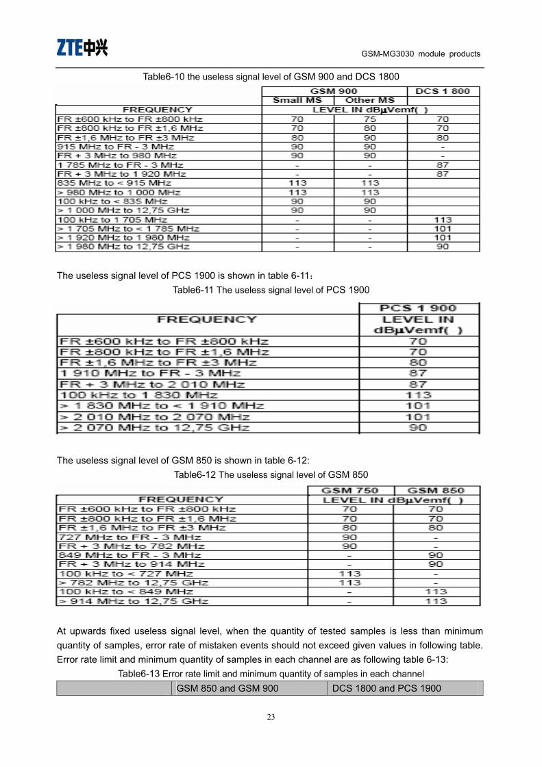
GSM-MG3030 module products
Table6-10 the useless signal level of GSM 900 and DCS 1800
The useless signal level of PCS 1900 is shown in table 6-11
Table6-11 The useless signal level of PCS 1900
The useless signal level of GSM 850 is shown in table 6-12:
Table6-12 The useless signal level of GSM 850
At upwards fixed useless signal level, when the quantity of tested samples is less than minimum
quantity of samples, error rate of mistaken events should not exceed given values in following table.
Error rate limit and minimum quantity of samples in each channel are as following table 6-13:
Table6-13 Error rate limit and minimum quantity of samples in each channel
GSM 850 and GSM 900 DCS 1800 and PCS 1900
23

GSM-MG3030 module products
channel Measure
type
FER limit % minimum
quantity of
samples
FER limit (%) minimum
quantity of
samples
TCH/FS II
type
RBER 2.439 8200
FACCH/F FER 8.961 6696 4.368 13736
Spurious respond
In the range of FR±45MHz frequency not including FR±800kHz under normal test condition:
1. for GSM 850 and GSM900, 6 failed frequencies are permitted
2. for DCS1800 and PCS 1900, 12 failed frequencies are permitted
3. for GSM 850 in the range of 100kHz~849MHz and 914MHz~12.75GHz, under normal test
condition, 24 failed frequencies are permitted if failed frequencies continue as a group, the
number of frequencies in each group could not more than 3.
4. for GSM 900 in the range of 100kHz~915MHz and 980MHz~12.75GHz, under normal test
condition, 24 failed frequencies are permitted if failed frequencies continue as a group, the
number of frequencies in each group could not more than 3.
5. for DCS 1800 in the range of 100kHz~785MHz and 1920MHz~12.75GHz, under normal test
condition, 24 failed frequencies are permitted if failed frequencies continue as a group, the
number of frequencies in each group could not more than 3.
6. for GSM 850 in the range of 100kHz~1910MHz and 2010MHz~12.75GHz, under normal test
condition, 24 failed frequencies are permitted if failed frequencies continue as a group, the
number of frequencies in each group could not more than 3.
Upwards failed frequencies are spurious respond frequencies, when the interference signal level
decrease to 70dB V emf at these frequencies, error rate of mistaken events should not exceed
values given in table 6-13
6.4 Recommendation of antenna specs
The recommended antenna specs are as following table 6-14:
Table6-14 recommended antenna specs
VSWR 1.5:1 maximum
gain At least 0 dBi in one direction
Input impedance 50#
Polarized form Vertical polarizing
The requirements for antenna’s gain are different in different environment. Commonly, in used
frequency range, the larger gain, the better capability; otherwise, out of this range, the smaller gain,
the better capability.
The antenna seat’s type of MG3030 module is MM9329-2700B.
24

GSM-MG3030 module products
6.5 Power supply
6.5.1 Input voltage
The input voltage is shown in table 6-15:
Table6-15 input voltage
state Max. voltage Typical voltage Min. voltage
Power supply 4.25 VDC 3.90 VDC 3.30 VDC
6.6 Working conditions
Working temperature:-20 ~ +55
Storage temperature:-40 ~ +70
humidity 5% ~ 95%
7 Reliability test standard
7.1 Low temperature running experiment
Required Temperature: -20
Duration Time: 16H
Reference standard GB/T 2423.1-2001
7.2 Low temperature storage experiment
Required Temperature: -40
Duration Time: 24H
Reference standard GB/T 2423.1-2001
7.3 High temperature running experiment
Required Temperature: +80
Duration Time: 16H
Reference standard GB/T 2423.2-2001
7.4 High temperature storage experiment
Required Temperature: +85
Duration Time: 24H
Reference standard GB/T 2423.2-2001
25

GSM-MG3030 module products
7.5 High temperature, high humidity experiment
Required Temperature: +40
Required Humidity: 85%RH
Duration Time: 48H
Reference standard GB/T 2423.2-2001
7.6 High-low temperature striking experiment
Cycles: 5
Temperature Range: -20 ~ +80
Duration Time: 2h
recovery time: 2h
Reference standard GB/T 2423.3-2001
8 EMC/EMI test standard
8.1 Static discharge ESD interference immunity experiment
Experiment level stated experiment levels are shown in table8-1 this product use level 4.
Table8-1 static experiment level
Touch discharge Air discharge
level Experiment
voltage (kV) level Experiment voltage (kV)
1 2 1 2
2 4 2 4
3 6 3 8
4 8 4 15
X special X special
8.2 RF electromagnetic emission interference immunity experiment
Experiment level stated experiment levels are shown in table8-2 this product use level 3.
Table8-2 emission anti-interference experiment level
Level Experiment field power V/m
1 1
2 3
3 10
X exclusive
notice: the frequency range is80MHz 1000MHz
26

GSM-MG3030 module products
8.3 Electrical fast transient/burst immunity experiment
Experiment level stated experiment levels are shown in table8-3 this product use level 3.
Table8-3 Electrical fast-changed pulse group anti-interference experiment level
Level Power supply and ground
protection ports Signal and control ports
Peak value of
voltage (kV)
Repeat ratio
(kHz)
Peak value of voltage
(kV) Repeat ratio(kHz)
1 0.5 5 0.25 5
2 1 5 0.5 5
3 2 5 1 5
4 4 2.5 2 5
5 special special special special
8.4 Lightning and surge strike immunity experiment
Experiment level stated experiment levels are shown in table8-4 this product use level 2.
Table8-4 Lightning and surge strike anti-interference experiment
Level Open-circuit experiment voltage(kV)
1 0.5
2 1.0
3 2.0
4 4.0
X special
Experiment wave shape 1.2/50us combine wave
8.5 RF electromagnetic field conduction interference immunity experiment
Experiment level stated experiment levels are shown in table8-5 this product use level 2.
Table8-5 conduction anti-interference experiment level
Level Experiment voltage V
1 1
2 3
3 10
X special
notice the frequency range is 0.15 80 MHz
Examine frequency range 0.15 230MHz
Frequency pace 1
modulation AM 1KHz 80
27

GSM-MG3030 module products
8.6 Radiated disturbance experiment
Demodulation method quasi-peak value demodulation, peak value demodulation.
Reference standard YD/T1169.1-2001 GB9254 1998
8.7 Conducted disturbance experiment
Demodulation method quasi-peak value demodulation, peak value demodulation, average value
demodulation, AC L
Reference standard YD/T1169.1-2001 GB9254 1998
28